i Sirius ISR35XX GSM/GPRS Module User Manual
i-Sirius Co.,Ltd GSM/GPRS Module Users Manual
UserManual.wiki
>
i Sirius
>
ISR35XX User Manual
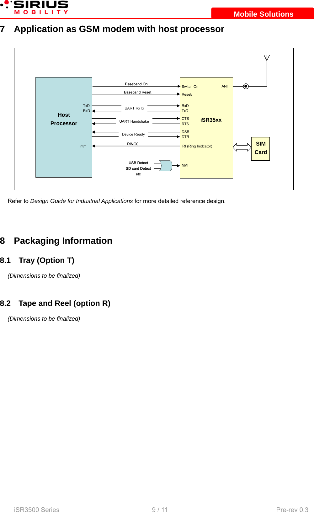
Users Manual
Navigation menu
Upload a User Manual
Namespaces
Wiki Guide
HTML
PDF
Info
Views
User Manual
Discussion / Help
Navigation