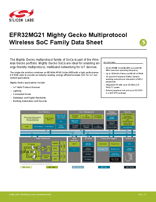
The detailed functional description can be found in the EFR32xG21 Reference Manual. A block diagram of the EFR32MG21 family is shown in Figure 3.1 Detailed EFR32MG21 Block Diagram on page 6. The diagram shows a superset of features available on the family, which vary by OPN. For more information about specific device features, consult
EFR32MG21A010F1024IM32-B • Bluetooth 5.1 • Zigbee • Thread 10 dBm @ 2.4 GHz 1024 96 Secure Ele-ment 20 QFN32 EFR32MG21A010F512IM32-B • Bluetooth 5.1 • Zigbee • Thread 10 dBm @ 2.4 GHz 512 64 Secure Ele-ment 20 QFN32 EFR32MG21A010F768IM32-B • Bluetooth 5.1 • Zigbee • Thread 10 dBm @ 2.4 GHz 768 64 Secure Ele-ment 20 QFN32
EFR32MG21 Mighty Gecko Multiprotocol Wireless SoC Family Data Sheet The Mighty Gecko multiprotocol family of SoCs is part of the Wireless Gecko portfolio. Mighty Gecko SoCs are ideal for enabling energy-friendly multiprotocol, multiband networking for IoT devices. The single-die solution combines an 80 MHz ARM Cortex-M33 with a high performance 2.4 GHz radio to provide an industry-leading, energy efficient wireless SoC for IoT connected applications. Mighty Gecko applications include: · IoT Multi-Protocol Devices · Lighting · Connected Home · Gateways and Digital Assistants · Building Automation and Security KEY FEATURES · 32-bit ARM® Cortex®-M33 core with 80 MHz maximum operating frequency · Up to 1024 kB of flash and 96 kB of RAM · 12-channel Peripheral Reflex System enabling autonomous interaction of MCU peripherals · Integrated PA with up to 20 dBm (2.4 GHz) TX power · Robust peripheral set and up to 20 GPIO in a 4x4 QFN package Core / Memory ARM CortexTM M33 processor with DSP extensions, FPU and Trust Zone Flash Program Memory Secure Boot with Root of Trust and Secure Loader EUI ETM Secure Debug RAM Memory LDMA Controller FRC BUFC Radio Transceiver RF Frontend I LNA Q PA PA DEMOD PGA IFADC Frequency Synth AGC MOD Lowest power mode with peripheral operational: EM0--Active EM1--Sleep CRC RAC Clock Management HF Crystal Oscillator EM23 HF RC Oscillator HF RC Oscillator Fast Startup RC Oscillator LF Crystal Oscillator Ultra LF RC Oscillator LF RC Oscillator Energy Management Voltage Regulator Brown-Out Detector Power-On Reset Security Crypto Acceleration True Random Number Generator DPA Countermeasures Secure Debug Authentication Secure Element 32-bit bus Peripheral Reflex System Serial Interfaces USART I/O Ports External Interrupts General I2C Purpose I/O Pin Reset Pin Wakeup Timers and Triggers Timer/Counter Protocol Timer Low Energy Timer Watchdog Timer Real Time Capture Counter Back-Up Real Time Counter Analog I/F IADC Analog Comparator EM2--Deep Sleep EM3--Stop EM4--Shutoff silabs.com | Building a more connected world. Rev. 1.1 1. Feature List The EFR32MG21 highlighted features are listed below. · Low Power Wireless System-on-Chip · High Performance 32-bit 80 MHz ARM Cortex®-M33 with DSP instruction and floating-point unit for efficient signal processing · Up to 1024 kB flash program memory · Up to 96 kB RAM data memory · 2.4 GHz radio operation · TX power up to 20 dBm · Low Energy Consumption · 8.8 mA RX current at 2.4 GHz (1 Mbps GFSK) · 9.4 mA RX current at 2.4 GHz (250 kbps O-QPSK DSSS) · 9.3 mA TX current @ 0 dBm output power at 2.4 GHz · 33.8 mA TX current @ 10 dBm output power at 2.4 GHz · 50.9 A/MHz in Active Mode (EM0) · 5.0 A EM2 DeepSleep current (96 kB RAM retention and RTC running from LFXO) · 4.5 A EM2 DeepSleep current (16 kB RAM retention and RTC running from LFRCO) · High Receiver Performance · -104.5 dBm sensitivity @ 250 kbps O-QPSK DSSS · -97.5 dBm sensitivity @ 1 Mbit/s GFSK · -94.4 dBm sensitivity @ 2 Mbit/s GFSK · -104.9 dBm sensitivity @ 125 kbps GFSK · Supported Modulation Formats · GFSK · OQPSK · Protocol Support · Bluetooth Low Energy (Bluetooth 5) · Zigbee · Thread EFR32MG21 Mighty Gecko Multiprotocol Wireless SoC Family Data Sheet Feature List · Wide selection of MCU peripherals · 12-bit 1 Msps SAR Analog to Digital Converter (ADC) · 2 × Analog Comparator (ACMP) · Up to 20 General Purpose I/O pins with output state retention and asynchronous interrupts · 8 Channel DMA Controller · 12 Channel Peripheral Reflex System (PRS) · 2 × 16-bit Timer/Counter · 3 Compare/Capture/PWM channels · 1 × 32-bit Timer/Counter · 3 Compare/Capture/PWM channels · 32-bit Real Time Counter · 24-bit Low Energy Timer for waveform generation · 2 × Watchdog Timer · 3 × Universal Synchronous/Asynchronous Receiver/Transmitter (UART/SPI/SmartCard(ISO 7816)/IrDA/I2S) · 2 × I2C interface with SMBus support · Wide Operating Range · 1.71 to 3.8 V single power supply · -40 to 125 °C ambient · Security · Secure Boot with Root of Trust and Secure Loader (RTSL) · Hardware Cryptographic Acceleration with DPA countermeasures for AES128/256, SHA-1, SHA-2 (up to 256-bit), ECC (up to 256-bit), ECDSA, ECDH and J-Pake · True Random Number Generator (TRNG) compliant with NIST SP800-90 and AIS-31 · ARM® TrustZone® · Secure Debug with lock/unlock · QFN32 4x4 mm Package · 0.4 mm pitch silabs.com | Building a more connected world. Rev. 1.1 | 2 2. Ordering Information Ordering Code EFR32MG21A010F1024IM32-B EFR32MG21A010F512IM32-B EFR32MG21A010F768IM32-B EFR32MG21A020F1024IM32-B EFR32MG21A020F512IM32-B EFR32MG21A020F768IM32-B EFR32MG21 Mighty Gecko Multiprotocol Wireless SoC Family Data Sheet Ordering Information Table 2.1. Ordering Information Max TX Power @ FreProtocol Stack quency Band · Bluetooth 5.1 · Zigbee · Thread 10 dBm @ 2.4 GHz · Bluetooth 5.1 · Zigbee · Thread 10 dBm @ 2.4 GHz · Bluetooth 5.1 · Zigbee · Thread 10 dBm @ 2.4 GHz · Bluetooth 5.1 · Zigbee · Thread 20 dBm @ 2.4 GHz · Bluetooth 5.1 · Zigbee · Thread 20 dBm @ 2.4 GHz · Bluetooth 5.1 · Zigbee · Thread 20 dBm @ 2.4 GHz Flash (kB) 1024 RAM Pack- (kB) Security GPIO age 96 Secure Ele- 20 QFN32 ment 512 64 Secure Ele- 20 QFN32 ment 768 64 Secure Ele- 20 QFN32 ment 1024 96 Secure Ele- 20 QFN32 ment 512 64 Secure Ele- 20 QFN32 ment 768 64 Secure Ele- 20 QFN32 ment silabs.com | Building a more connected world. Rev. 1.1 | 3 Table of Contents 1. Feature List . . . . . . . . . . . . . . . . . . . . . . . . . . . . . . . . 2 2. Ordering Information . . . . . . . . . . . . . . . . . . . . . . . . . . . . 3 3. System Overview . . . . . . . . . . . . . . . . . . . . . . . . . . . . . . 6 3.1 Introduction . . . . . . . . . . . . . . . . . . . . . . . . . . . . . . . 6 3.2 Radio . . . . . . . . . . . . . . . . . . . . . . . . . . . . . . . . . 6 3.2.1 Antenna Interface . . . . . . . . . . . . . . . . . . . . . . . . . . . 6 3.2.2 Fractional-N Frequency Synthesizer . . . . . . . . . . . . . . . . . . . . . 7 3.2.3 Receiver Architecture . . . . . . . . . . . . . . . . . . . . . . . . . . 7 3.2.4 Transmitter Architecture . . . . . . . . . . . . . . . . . . . . . . . . . 7 3.2.5 Packet and State Trace . . . . . . . . . . . . . . . . . . . . . . . . . 7 3.2.6 Data Buffering . . . . . . . . . . . . . . . . . . . . . . . . . . . . . 7 3.2.7 Radio Controller (RAC). . . . . . . . . . . . . . . . . . . . . . . . . . 7 3.3 General Purpose Input/Output (GPIO) . . . . . . . . . . . . . . . . . . . . . . 8 3.4 Clocking . . . . . . . . . . . . . . . . . . . . . . . . . . . . . . . . 8 3.4.1 Clock Management Unit (CMU) . . . . . . . . . . . . . . . . . . . . . . . 8 3.4.2 Internal and External Oscillators. . . . . . . . . . . . . . . . . . . . . . . 8 3.5 Counters/Timers and PWM . . . . . . . . . . . . . . . . . . . . . . . . . . 8 3.5.1 Timer/Counter (TIMER) . . . . . . . . . . . . . . . . . . . . . . . . . 8 3.5.2 Low Energy Timer (LETIMER) . . . . . . . . . . . . . . . . . . . . . . . 8 3.5.3 Real Time Clock with Capture (RTCC) . . . . . . . . . . . . . . . . . . . . 9 3.5.4 Back-Up Real Time Counter . . . . . . . . . . . . . . . . . . . . . . . . 9 3.5.5 Watchdog Timer (WDOG) . . . . . . . . . . . . . . . . . . . . . . . . . 9 3.6 Communications and Other Digital Peripherals . . . . . . . . . . . . . . . . . . . 9 3.6.1 Universal Synchronous/Asynchronous Receiver/Transmitter (USART) . . . . . . . . . . 9 3.6.2 Inter-Integrated Circuit Interface (I2C) . . . . . . . . . . . . . . . . . . . . . 9 3.6.3 Peripheral Reflex System (PRS) . . . . . . . . . . . . . . . . . . . . . . 9 3.7 Security Features . . . . . . . . . . . . . . . . . . . . . . . . . . . . . 9 3.7.1 Secure Boot with Root of Trust and Secure Loader (RTSL) . . . . . . . . . . . . .10 3.7.2 Cryptographic Accelerator. . . . . . . . . . . . . . . . . . . . . . . . .10 3.7.3 True Random Number Generator . . . . . . . . . . . . . . . . . . . . . .10 3.7.4 Secure Debug with Lock/Unlock. . . . . . . . . . . . . . . . . . . . . . .10 3.8 Analog. . . . . . . . . . . . . . . . . . . . . . . . . . . . . . . . .10 3.8.1 Analog Comparator (ACMP) . . . . . . . . . . . . . . . . . . . . . . . .10 3.8.2 Analog to Digital Converter (IADC) . . . . . . . . . . . . . . . . . . . . . .11 3.9 Reset Management Unit (RMU) . . . . . . . . . . . . . . . . . . . . . . . .11 3.10 Core and Memory . . . . . . . . . . . . . . . . . . . . . . . . . . . .11 3.10.1 Processor Core . . . . . . . . . . . . . . . . . . . . . . . . . . . .11 3.10.2 Memory System Controller (MSC) . . . . . . . . . . . . . . . . . . . . .11 3.10.3 Linked Direct Memory Access Controller (LDMA) . . . . . . . . . . . . . . . .11 3.11 Memory Map . . . . . . . . . . . . . . . . . . . . . . . . . . . . . .12 3.12 Configuration Summary . . . . . . . . . . . . . . . . . . . . . . . . . .13 silabs.com | Building a more connected world. Rev. 1.1 | 4 4. Electrical Specifications . . . . . . . . . . . . . . . . . . . . . . . . . . 14 4.1 Electrical Characteristics . . . . . . . . . . . . . . . . . . . . . . . . . .14 4.1.1 Absolute Maximum Ratings . . . . . . . . . . . . . . . . . . . . . . . .14 4.1.2 General Operating Conditions . . . . . . . . . . . . . . . . . . . . . . .15 4.1.3 Thermal Characteristics . . . . . . . . . . . . . . . . . . . . . . . . .16 4.1.4 Current Consumption . . . . . . . . . . . . . . . . . . . . . . . . . .17 4.1.5 2.4 GHz RF Transceiver Characteristics . . . . . . . . . . . . . . . . . . . .22 4.1.6 Flash Characteristics . . . . . . . . . . . . . . . . . . . . . . . . . .37 4.1.7 Wake Up, Entry, and Exit times . . . . . . . . . . . . . . . . . . . . . . .38 4.1.8 Oscillators . . . . . . . . . . . . . . . . . . . . . . . . . . . . . .39 4.1.9 GPIO Pins (3V GPIO pins) . . . . . . . . . . . . . . . . . . . . . . . .44 4.1.10 Analog to Digital Converter (ADC) . . . . . . . . . . . . . . . . . . . . .45 4.1.11 Analog Comparator (ACMP) . . . . . . . . . . . . . . . . . . . . . . .47 4.1.12 Temperature Sense . . . . . . . . . . . . . . . . . . . . . . . . . .48 4.1.13 Brown Out Detectors . . . . . . . . . . . . . . . . . . . . . . . . . .49 4.1.14 SPI Electrical Specifications . . . . . . . . . . . . . . . . . . . . . . .51 4.1.15 I2C Electrical Specifications. . . . . . . . . . . . . . . . . . . . . . . .52 4.2 Typical Performance Curves . . . . . . . . . . . . . . . . . . . . . . . . .54 4.2.1 Supply Current . . . . . . . . . . . . . . . . . . . . . . . . . . . .55 4.2.2 2.4 GHz Radio . . . . . . . . . . . . . . . . . . . . . . . . . . . .57 5. Typical Connection Diagrams . . . . . . . . . . . . . . . . . . . . . . . . 60 5.1 Power . . . . . . . . . . . . . . . . . . . . . . . . . . . . . . . . .60 5.2 RF Matching Networks . . . . . . . . . . . . . . . . . . . . . . . . . . .60 5.2.1 2.4 GHz 0 dBm Matching Network . . . . . . . . . . . . . . . . . . . . . .60 5.2.2 2.4 GHz 10 dBm Matching Network . . . . . . . . . . . . . . . . . . . . .61 5.2.3 2.4 GHz 20 dBm Matching Network . . . . . . . . . . . . . . . . . . . . .62 5.3 Other Connections. . . . . . . . . . . . . . . . . . . . . . . . . . . . .62 6. Pin Definitions . . . . . . . . . . . . . . . . . . . . . . . . . . . . . . 63 6.1 QFN32 2.4GHz Device Pinout . . . . . . . . . . . . . . . . . . . . . . . . .63 6.2 Alternate Function Table. . . . . . . . . . . . . . . . . . . . . . . . . . .64 6.3 Analog Peripheral Connectivity . . . . . . . . . . . . . . . . . . . . . . . .65 6.4 Digital Peripheral Connectivity . . . . . . . . . . . . . . . . . . . . . . . . .66 7. QFN32 Package Specifications. . . . . . . . . . . . . . . . . . . . . . . . 69 7.1 QFN32 Package Dimensions . . . . . . . . . . . . . . . . . . . . . . . . .69 7.2 QFN32 PCB Land Pattern . . . . . . . . . . . . . . . . . . . . . . . . . .71 7.3 QFN32 Package Marking . . . . . . . . . . . . . . . . . . . . . . . . . .73 8. Revision History . . . . . . . . . . . . . . . . . . . . . . . . . . . . . 74 silabs.com | Building a more connected world. Rev. 1.1 | 5 3. System Overview EFR32MG21 Mighty Gecko Multiprotocol Wireless SoC Family Data Sheet System Overview 3.1 Introduction The EFR32 product family combines an energy-friendly MCU with a high performance radio transceiver. The devices are well suited for secure connected IoT multiprotocol devices requiring high performance and low energy consumption. This section gives a short introduction to the full radio and MCU system. The detailed functional description can be found in the EFR32xG21 Reference Manual. A block diagram of the EFR32MG21 family is shown in Figure 3.1 Detailed EFR32MG21 Block Diagram on page 6. The diagram shows a superset of features available on the family, which vary by OPN. For more information about specific device features, consult Ordering Information. RF2G4_IO1 RF2G4_IO2 RESETn Debug Signals (shared w/GPIO) PAVDD RFVDD IOVDD AVDD DVDD DECOUPLE LFXTAL_I LFXTAL_O HFXTAL_I HFXTAL_O FRC BUFC Radio Transciever RF Frontend I LNA Q PGA PA PA Frequency Synthesizer DEMOD IFADC AGC MOD CRC RAC Serial Wire and ETM Debug / Programming Reset Management Unit Brown Out / Power-On Reset Energy Management Voltage Regulator ARM Cortex-M33 Core Up to 1024 kB Flash Program Memory Up to 96 KB RAM Trust Zone Floating Point Unit DMA Controller Watchdog Timer Clock Management ULFRCO FSRCO HFRCOEM2 LFRCO LFXO HFRCO HFXO AA HP BB Port I/O Configuration Digital Peripherals LETIMER TIMER RTC USART I2C Port Mapper Crypto Accelerator TRNG CRC Analog Peripherals Internal Reference 12-bit ADC VDD + Analog Comparator Input Mux Port Mapper IOVDD Port A Drivers PAn Port B Drivers PBn Port C Drivers PCn Port D Drivers PDn Figure 3.1. Detailed EFR32MG21 Block Diagram 3.2 Radio The EFR32MG21 Mighty Gecko features a highly configurable radio transceiver supporting Zigbee, Thread, and Bluetooth Low Energy wireless protocols. 3.2.1 Antenna Interface The 2.4 GHz antenna interface consists of two single-ended pins (RF2G4_IO1 and RF2G4_IO2) that interface directly to two LNAs and two 10 dBm PAs. For devices that support 20 dBm, these pins also interface to the 20 dBm on-chip balun. Integrated switches select either RF2G4_IO1 or RF2G4_IO2 to be the active path. The external components and power supply connections for the antenna interface typical applications are shown in the RF Matching Networks section. silabs.com | Building a more connected world. Rev. 1.1 | 6 EFR32MG21 Mighty Gecko Multiprotocol Wireless SoC Family Data Sheet System Overview 3.2.2 Fractional-N Frequency Synthesizer The EFR32MG21 contains a high performance, low phase noise, fully integrated fractional-N frequency synthesizer. The synthesizer is used in receive mode to generate the LO frequency for the down-conversion mixer. It is also used in transmit mode to directly generate the modulated RF carrier. The fractional-N architecture provides excellent phase noise performance, frequency resolution better than 100 Hz, and low energy consumption. The synthesizer's fast frequency settling allows for very short receiver and transmitter wake up times to reduce system energy consumption. 3.2.3 Receiver Architecture The EFR32MG21 uses a low-IF receiver architecture, consisting of a Low-Noise Amplifier (LNA) followed by an I/Q down-conversion mixer. The I/Q signals are further filtered and amplified before being sampled by the IF analog-to-digital converter (IFADC). The IF frequency is configurable from 150 kHz to 1371 kHz. The IF can further be configured for high-side or low-side injection, providing flexibility with respect to known interferers at the image frequency. The Automatic Gain Control (AGC) module adjusts the receiver gain to optimize performance and avoid saturation for excellent selectivity and blocking performance. The 2.4 GHz radio is calibrated at production to improve image rejection performance. Demodulation is performed in the digital domain. The demodulator performs configurable decimation and channel filtering to allow receive bandwidths ranging from 0.1 to 2530 kHz. High carrier frequency and baud rate offsets are tolerated by active estimation and compensation. Advanced features supporting high quality communication under adverse conditions include forward error correction by block and convolutional coding as well as Direct Sequence Spread Spectrum (DSSS). A Received Signal Strength Indicator (RSSI) is available for signal quality metrics, for level-based proximity detection, and for RF channel access by Collision Avoidance (CA) or Listen Before Talk (LBT) algorithms. An RSSI capture value is associated with each received frame and the dynamic RSSI measurement can be monitored throughout reception. 3.2.4 Transmitter Architecture The EFR32MG21 uses a direct-conversion transmitter architecture. For constant envelope modulation formats, the modulator controls phase and frequency modulation in the frequency synthesizer. Transmit symbols or chips are optionally shaped by a digital shaping filter. The shaping filter is fully configurable, including the BT product, and can be used to implement Gaussian or Raised Cosine shaping. Carrier Sense Multiple Access - Collision Avoidance (CSMA-CA) or Listen Before Talk (LBT) algorithms can be automatically timed by the EFR32MG21. These algorithms are typically defined by regulatory standards to improve inter-operability in a given bandwidth between devices that otherwise lack synchronized RF channel access. 3.2.5 Packet and State Trace The EFR32MG21 Frame Controller has a packet and state trace unit that provides valuable information during the development phase. It features: · Non-intrusive trace of transmit data, receive data and state information · Data observability on a single-pin UART data output, or on a two-pin SPI data output · Configurable data output bitrate / baudrate · Multiplexed transmitted data, received data and state / meta information in a single serial data stream 3.2.6 Data Buffering The EFR32MG21 features an advanced Radio Buffer Controller (BUFC) capable of handling up to 4 buffers of adjustable size from 64 bytes to 4096 bytes. Each buffer can be used for RX, TX or both. The buffer data is located in RAM, enabling zero-copy operations. 3.2.7 Radio Controller (RAC) The Radio Controller controls the top level state of the radio subsystem in the EFR32MG21. It performs the following tasks: · Precisely-timed control of enabling and disabling of the receiver and transmitter circuitry · Run-time calibration of receiver, transmitter and frequency synthesizer · Detailed frame transmission timing, including optional LBT or CSMA-CA silabs.com | Building a more connected world. Rev. 1.1 | 7 EFR32MG21 Mighty Gecko Multiprotocol Wireless SoC Family Data Sheet System Overview 3.3 General Purpose Input/Output (GPIO) EFR32MG21 has up to 20 General Purpose Input/Output pins. Each GPIO pin can be individually configured as either an output or input. More advanced configurations including open-drain, open-source, and glitch-filtering can be configured for each individual GPIO pin. The GPIO pins can be overridden by peripheral connections, like SPI communication. Each peripheral connection can be routed to several GPIO pins on the device. The input value of a GPIO pin can be routed through the Peripheral Reflex System to other peripherals. The GPIO subsystem supports asynchronous external pin interrupts. All of the pins on ports A and port B are EM2 capable. These pins may be used by Low-Energy peripherals in EM2/3 and may also be used as EM2/3 pin wake-ups. Pins on ports C and D are latched/retained in their current state when entering EM2 until EM2 exit upon which internal peripherals could once again drive those pads. A few GPIOs also have EM4 wake functionality. These pins are listed in 6.2 Alternate Function Table. 3.4 Clocking 3.4.1 Clock Management Unit (CMU) The Clock Management Unit controls oscillators and clocks in the EFR32MG21. Individual enabling and disabling of clocks to all peripheral modules is performed by the CMU. The CMU also controls enabling and configuration of the oscillators. A high degree of flexibility allows software to optimize energy consumption in any specific application by minimizing power dissipation in unused peripherals and oscillators. 3.4.2 Internal and External Oscillators The EFR32MG21 supports two crystal oscillators and fully integrates five RC oscillators, listed below. · A high frequency crystal oscillator (HFXO) with integrated load capacitors, tunable in small steps, provides a precise timing refer- ence for the MCU and RF synthesizer. The HFXO provides excellent RF clocking performance using a 38.4 MHz crystal. The HFXO can also support an external clock source such as a TCXO for applications that require an extremely accurate clock frequency over temperature. · A 32.768 kHz crystal oscillator (LFXO) provides an accurate timing reference for low energy modes. · An integrated high frequency RC oscillator (HFRCO) is available for the MCU system, when crystal accuracy is not required. The HFRCO employs fast start-up at minimal energy consumption combined with a wide frequency range, from 1 MHz to 80 MHz. · An integrated high frequency RC oscillator (HFRCOEM2) runs down to EM2 and is available for timing the general-purpose ADC and the Serial Wire Viewer port with a wide frequency range. · An integrated fast start-up RC oscillator (FSRCO) that runs at a fixed 20 MHz · An integrated low frequency 32.768 kHz RC oscillator (LFRCO) for low power operation where high accuracy is not required. · An integrated ultra-low frequency 1 kHz RC oscillator (ULFRCO) is available to provide a timing reference at the lowest energy consumption in low energy modes. 3.5 Counters/Timers and PWM 3.5.1 Timer/Counter (TIMER) TIMER peripherals keep track of timing, count events, generate PWM outputs and trigger timed actions in other peripherals through the Peripheral Reflex System (PRS). The core of each TIMER is a 16-bit or 32-bit counter with up to 3 compare/capture channels. Each channel is configurable in one of three modes. In capture mode, the counter state is stored in a buffer at a selected input event. In compare mode, the channel output reflects the comparison of the counter to a programmed threshold value. In PWM mode, the TIMER supports generation of pulse-width modulation (PWM) outputs of arbitrary waveforms defined by the sequence of values written to the compare registers. In addition some timers offer dead-time insertion. See 3.12 Configuration Summary for information on the feature set of each timer. 3.5.2 Low Energy Timer (LETIMER) The unique LETIMER is a 24-bit timer that is available in energy mode EM2 Deep Sleep in addition to EM1 Sleep and EM0 Active. This allows it to be used for timing and output generation when most of the device is powered down, allowing simple tasks to be performed while the power consumption of the system is kept at an absolute minimum. The LETIMER can be used to output a variety of waveforms with minimal software intervention. The LETIMER is connected to the Peripheral Reflex System (PRS), and can be configured to start counting on compare matches from other peripherals such as the RTCC. silabs.com | Building a more connected world. Rev. 1.1 | 8 EFR32MG21 Mighty Gecko Multiprotocol Wireless SoC Family Data Sheet System Overview 3.5.3 Real Time Clock with Capture (RTCC) The Real Time Clock with Capture (RTCC) is a 32-bit counter providing timekeeping down to EM3. The RTCC can be clocked by any of the on-board low-frequency oscillators, and it is capable of providing system wake-up at user defined intervals. A secondary RTC is used by the RF protocol stack for event scheduling, leaving the primary RTCC block available exclusively for application software. 3.5.4 Back-Up Real Time Counter The Back-Up Real Time Counter (BURTC) is a 32-bit counter providing timekeeping in all energy modes, including EM4. The BURTC can be clocked by any of the on-board low-frequency oscillators, and it is capable of providing system wake-up at user defined invervals. 3.5.5 Watchdog Timer (WDOG) The watchdog timer can act both as an independent watchdog or as a watchdog synchronous with the CPU clock. It has windowed monitoring capabilities, and can generate a reset or different interrupts depending on the failure mode of the system. The watchdog can also monitor autonomous systems driven by the Peripheral Reflex System (PRS). 3.6 Communications and Other Digital Peripherals 3.6.1 Universal Synchronous/Asynchronous Receiver/Transmitter (USART) The Universal Synchronous/Asynchronous Receiver/Transmitter is a flexible serial I/O module. It supports full duplex asynchronous UART communication with hardware flow control as well as RS-485, SPI, MicroWire and 3-wire. It can also interface with devices supporting: · ISO7816 SmartCards · IrDA · I2S 3.6.2 Inter-Integrated Circuit Interface (I2C) The I2C module provides an interface between the MCU and a serial I2C bus. It is capable of acting as both a master and a slave and supports multi-master buses. Standard-mode, fast-mode and fast-mode plus speeds are supported, allowing transmission rates from 10 kbit/s up to 1 Mbit/s. Slave arbitration and timeouts are also available, allowing implementation of an SMBus-compliant system. The interface provided to software by the I2C module allows precise timing control of the transmission process and highly automated transfers. Automatic recognition of slave addresses is provided in active and low energy modes. Note that not all instances of I2C are avaliable in all energy modes. 3.6.3 Peripheral Reflex System (PRS) The Peripheral Reflex System provides a communication network between different peripheral modules without software involvement. Peripheral modules producing Reflex signals are called producers. The PRS routes Reflex signals from producers to consumer peripherals which in turn perform actions in response. Edge triggers and other functionality such as simple logic operations (AND, OR, NOT) can be applied by the PRS to the signals. The PRS allows peripherals to act autonomously without waking the MCU core, saving power. 3.7 Security Features A dedicated security CPU enables the Secure Element function. It isolates cryptographic functions and data from the host Cortex-M33 core and provides the following security features: · Secure Boot with Root of Trust and Secure Loader (RTSL) · Cryptographic Accelerator · True Random Number Generator (TRNG) · Secure Debug with Lock/Unlock silabs.com | Building a more connected world. Rev. 1.1 | 9 EFR32MG21 Mighty Gecko Multiprotocol Wireless SoC Family Data Sheet System Overview 3.7.1 Secure Boot with Root of Trust and Secure Loader (RTSL) The Secure Boot with RTSL authenticates a chain of trusted firmware that begins from an immutable memory (ROM). It prevents malware injection, prevents rollback, ensures that only authentic firmware is executed and protects Over The Air updates. More information on this feature can be found in the Application Note AN1218: Series 2 Secure Boot with RTSL. 3.7.2 Cryptographic Accelerator The Cryptographic Accelerator is an autonomous hardware accelerator with Differential Power Analysis (DPA) countermeasures to protect keys. It supports AES encryption and decryption with 128/192/256-bit keys, Elliptic Curve Cryptography(ECC) to support public key operations and hashes. Supported block cipher modes of operation for AES include: · ECB (Electronic Code Book) · CTR (Counter Mode) · CBC (Cipher Block Chaining) · CFB (Cipher Feedback) · GCM (Galois Counter Mode) · CBC-MAC (Cipher Block Chaining Message Authentication Code) · GMAC (Galois Message Authentication Code) · CCM (Counter with CBC-MAC) The Cryptographic Accelerator accelerates Elliptical Curve Cryptography and supports the NIST (National Institute of Standards and Technology) recommended curves including P-192 and P-256 for ECDH(Elliptic Curve Diffie-Hellman) key derivation and ECDSA (Elliptic Curve Digital Signature Algorithm) sign and verify operations. Supported hashes include SHA-1, SHA2/224, and SHA-2/256. This implementation provides a fast and energy efficient solution to state of the art cryptographic needs. 3.7.3 True Random Number Generator The True Random Number Generator module is a non-deterministic random number generator that harvests entropy from a thermal energy source. It includes start-up health tests for the entropy source as required by NIST SP800-90B and AIS-31 as well as online health tests required for NIST SP800-90C. The TRNG is suitable for periodically generating entropy to seed an approved pseudo random number generator. 3.7.4 Secure Debug with Lock/Unlock For obvious security reasons, it is critical for a product to have its debug interface locked before being released in the field. In addition, the Secure Element also provides a secure debug unlock function that allows authenticated access based on public key cryptography. This functionality is particularly useful for supporting failure analysis while maintaining confidentiality of IP and sensitive end-user data. More information on this feature can be found in the Application Note AN1190: EFR32xG21 Secure Debug. 3.8 Analog 3.8.1 Analog Comparator (ACMP) The Analog Comparator is used to compare the voltage of two analog inputs, with a digital output indicating which input voltage is higher. Inputs are selected from among internal references and external pins. The tradeoff between response time and current consumption is configurable by software. Two 6-bit reference dividers allow for a wide range of internally-programmable reference sources. The ACMP can also be used to monitor the supply voltage. An interrupt can be generated when the supply falls below or rises above the programmable threshold. silabs.com | Building a more connected world. Rev. 1.1 | 10 EFR32MG21 Mighty Gecko Multiprotocol Wireless SoC Family Data Sheet System Overview 3.8.2 Analog to Digital Converter (IADC) The IADC is a hybrid architecture combining techniques from both SAR and Delta-Sigma style converters. It has a resolution of up to 12 bits at up to 1 Msps. Hardware oversampling reduces system-level noise over multiple front-end samples. The IADC includes integrated voltage references. Inputs are selectable from a wide range of sources, including pins configurable as either single-ended or differential. 3.9 Reset Management Unit (RMU) The RMU is responsible for handling reset of the EFR32MG21. A wide range of reset sources are available, including several power supply monitors, pin reset, software controlled reset, core lockup reset, and watchdog reset. 3.10 Core and Memory 3.10.1 Processor Core The ARM Cortex-M processor includes a 32-bit RISC processor integrating the following features and tasks in the system: · ARM Cortex-M33 RISC processor achieving 1.50 Dhrystone MIPS/MHz · ARM TrustZone security technology · Embedded Trace Macrocell (ETM) for real-time trace and debug · Up to 1024 kB flash program memory · Up to 96 kB RAM data memory · Configuration and event handling of all modules · 2-pin Serial-Wire debug interface 3.10.2 Memory System Controller (MSC) The Memory System Controller (MSC) is the program memory unit of the microcontroller. The flash memory is readable and writable from both the Cortex-M and DMA. In addition to the main flash array where Program code is normally written the MSC also provides an Information block where additional information such as special user information or flash-lock bits are stored. There is also a read-only page in the information block containing system and device calibration data. Read and write operations are supported in energy modes EM0 Active and EM1 Sleep. 3.10.3 Linked Direct Memory Access Controller (LDMA) The Linked Direct Memory Access (LDMA) controller allows the system to perform memory operations independently of software. This reduces both energy consumption and software workload. The LDMA allows operations to be linked together and staged, enabling sophisticated operations to be implemented. silabs.com | Building a more connected world. Rev. 1.1 | 11 EFR32MG21 Mighty Gecko Multiprotocol Wireless SoC Family Data Sheet System Overview 3.11 Memory Map The EFR32MG21 memory map is shown in the figures below. RAM and flash sizes are for the largest memory configuration. Figure 3.2. EFR32MG21 Memory Map -- Core Peripherals and Code Space silabs.com | Building a more connected world. Rev. 1.1 | 12 EFR32MG21 Mighty Gecko Multiprotocol Wireless SoC Family Data Sheet System Overview 3.12 Configuration Summary The features of the EFR32MG21 are a subset of the feature set described in the device reference manual. The table below describes device specific implementation of the features. Remaining modules support full configuration. Table 3.1. Configuration Summary Module TIMER0 TIMER1 TIMER2 USART0 USART1 USART2 I2C0 I2C1 Lowest Energy Mode EM1 EM1 EM1 EM1 EM1 EM1 EM2 EM1 Configuration 32-bit, 3-channels, +DTI 16-bit, 3-channels, +DTI 16-bit, 3-channels, +DTI +IrDA, +I2S, +SmartCard +IrDA, +I2S, +SmartCard +IrDA, +I2S, +SmartCard silabs.com | Building a more connected world. Rev. 1.1 | 13 4. Electrical Specifications EFR32MG21 Mighty Gecko Multiprotocol Wireless SoC Family Data Sheet Electrical Specifications 4.1 Electrical Characteristics All electrical parameters in all tables are specified under the following conditions, unless stated otherwise: · Typical values are based on TA=25 °C and all supplies at 3.0 V, by production test and/or technology characterization. · Radio performance numbers are measured in conducted mode, based on Silicon Laboratories reference designs using output pow- er-specific external RF impedance-matching networks for interfacing to a 50 antenna. · Minimum and maximum values represent the worst conditions across supply voltage, process variation, and operating temperature, unless stated otherwise. 4.1.1 Absolute Maximum Ratings Stresses above those listed below may cause permanent damage to the device. This is a stress rating only and functional operation of the devices at those or any other conditions above those indicated in the operation listings of this specification is not implied. Exposure to maximum rating conditions for extended periods may affect device reliability. For more information on the available quality and reliability data, see the Quality and Reliability Monitor Report at http://www.silabs.com/support/quality/pages/default.aspx. Table 4.1. Absolute Maximum Ratings Parameter Symbol Storage temperature range TSTG Junction temperature TJMAX Voltage on any supply pin VDDMAX Voltage ramp rate on any supply pin VDDRAMPMAX Voltage on HFXO pins VHFXOPIN DC voltage on any GPIO pin VDIGPIN Test Condition -I grade Input RF level on pins RF2G4_IO1 and RF2G4_IO2 PRFMAX2G4 Absolute voltage on RF pins VMAX2G4 RF2G4_IOx Total current into VDD power IVDDMAX lines Total current into VSS ground lines IVSSMAX Current per I/O pin IIOMAX Current for all I/O pins IIOALLMAX Source Sink Sink Source Sink Source Min Typ Max Unit -50 -- +150 °C -- -- +135 °C -0.3 -- 3.8 V -- -- 1.0 V / µs -0.3 -- 1.2 V -0.3 -- VIOVDD + V 0.3 -- -- +10 dBm -0.3 -- VPAVDD V -- -- 200 mA -- -- 200 mA -- -- 50 mA -- -- 50 mA -- -- 200 mA -- -- 200 mA silabs.com | Building a more connected world. Rev. 1.1 | 14 EFR32MG21 Mighty Gecko Multiprotocol Wireless SoC Family Data Sheet Electrical Specifications 4.1.2 General Operating Conditions This table specifies the general operating temperature range and supply voltage range for all supplies. The minimum and maximum values of all other tables are specifed over this operating range, unless otherwise noted. Table 4.2. General Operating Conditions Parameter Symbol Test Condition Min Typ Max Unit Operating ambient tempera- TA ture range -I temperature grade 1 -40 -- +125 ° C DVDD supply voltage VDVDD EM0/1 EM2/3/42 1.71 3.0 1.71 3.0 3.8 V 3.8 V AVDD supply voltage VAVDD 1.71 3.0 3.8 V IOVDDx operating supply voltage (All IOVDD pins) VIOVDDx 1.71 3.0 3.8 V PAVDD operating supply voltage VPAVDD 1.71 3.0 3.8 V RFVDD operating supply voltage VRFVDD 1.71 3.0 VPAVDD V DECOUPLE output capaci- CDECOUPLE tor3 0.75 1.0 2.75 µF HCLK and Core frequency fHCLK MODE = WS1, RAMWSEN = 14 -- -- 80 MHz MODE = WS1, RAMWSEN = 04 -- -- 50 MHz MODE = WS0, RAMWSEN = 04 -- -- 39 MHz PCLK frequency fPCLK -- -- 50 MHz EM01 Group A clock frequency fEM01GRPACLK -- -- 80 MHz HCLK Radio frequency5 fHCLKRADIO 38 38.4 40 MHz Note: 1. The device may operate continuously at the maximum allowable ambient TA rating as long as the absolute maximum TJMAX is not exceeded. For an application with significant power dissipation, the allowable TA may be lower than the maximum TA rating. TA = TJMAX - (THETAJA x PowerDissipation). Refer to the Absolute Maximum Ratings table and the Thermal Characteristics table for TJMAX and THETAJA. 2. The DVDD supply is monitored by the DVDD BOD in EM0/1 and the LE DVDD BOD in EM2/3/4. 3. The system designer should consult the characteristic specs of the capacitor used on DECOUPLE to ensure its capacitance value stays within the specified bounds across temperature and DC bias. 4. Flash wait states are set by the MODE field in the MSC_READCTRL register. RAM wait states are enabled by setting the RAMWSEN bit in the SYSYCFG_DMEM0RAMCTRL register. 5. The recommended radio crystal frequency is 38.4 MHz. Any crystal frequency other than 38.4 is expressly not supported. The minimum and maximum HCLKRADIO frequency in this table represent the design limits, which are much wider than the typical crystal tolerance. silabs.com | Building a more connected world. Rev. 1.1 | 15 4.1.3 Thermal Characteristics EFR32MG21 Mighty Gecko Multiprotocol Wireless SoC Family Data Sheet Electrical Specifications Table 4.3. Thermal Characteristics Parameter Symbol Test Condition Min Typ Max Unit Thermal Resistance Junction THE- 2-Layer PCB, Natural Convection1 -- to Ambient QFN32 (4x4mm) Package TAJA_QFN32_4X4 4-Layer PCB, Natural Convection1 -- 94.3 35.4 -- °C/W -- °C/W Thermal Resistance Junction THE- 2-Layer PCB, Natural Convection1 -- to Case QFN32 (4x4mm) Package TAJC_QFN32_4X4 4-Layer PCB, Natural Convection1 -- 36.3 23.5 -- °C/W -- °C/W Note: 1. Measured according to JEDEC standard JESD51-2A. Integrated Circuit Thermal Test Method Environmental Conditions - Natural Convection (Still Air). silabs.com | Building a more connected world. Rev. 1.1 | 16 4.1.4 Current Consumption EFR32MG21 Mighty Gecko Multiprotocol Wireless SoC Family Data Sheet Electrical Specifications 4.1.4.1 MCU current consumption at 1.8V Unless otherwise indicated, typical conditions are: AVDD = DVDD = RFVDD = PAVDD = 1.8V. TA = 25 °C. Minimum and maximum values in this table represent the worst conditions across process variation at TA = 25 °C. Table 4.4. MCU current consumption at 1.8V Parameter Symbol Current consumption in EM0 IACTIVE mode with all peripherals disabled1 Current consumption in EM1 IEM1 mode with all peripherals disabled1 Current consumption in EM2 IEM2 mode Current consumption in EM3 IEM3 mode Current consumption in EM4 IEM4 mode Current consumption during IRST reset Test Condition Min 80 MHz HFRCO, CPU running -- Prime from flash 80 MHz HFRCO, CPU running -- while loop from flash 80 MHz HFRCO, CPU running -- CoreMark loop from flash 38.4 MHz crystal, CPU running -- while loop from flash 38 MHz HFRCO, CPU running -- while loop from flash 26 MHz HFRCO, CPU running -- while loop from flash 16 MHz HFRCO, CPU running -- while loop from flash 1 MHz HFRCO, CPU running -- while loop from flash 80 MHz HFRCO -- 38.4 MHz crystal -- 38 MHz HFRCO -- 26 MHz HFRCO -- 16 MHz HFRCO -- 1 MHz HFRCO -- Full RAM retention and RTC run- -- ning from LFXO Full RAM retention and RTC run- -- ning from LFRCO 1 bank (16kB) RAM retention and -- RTC running from LFRCO Full RAM retention and RTC run- -- ning from ULFRCO 1 bank (16kB) RAM retention and -- RTC running from ULFRCO No BURTC, no LF oscillator -- BURTC with LFXO -- Hard pin reset held -- Typ 50.9 45.5 59.7 63.6 55.5 59.1 67.0 360 28.7 46.7 38.7 42.2 50.0 343 5.0 5.0 4.5 4.7 4.2 0.14 0.51 107 Max Unit -- µA/MHz -- µA/MHz -- µA/MHz -- µA/MHz -- µA/MHz -- µA/MHz -- µA/MHz -- µA/MHz -- µA/MHz -- µA/MHz -- µA/MHz -- µA/MHz -- µA/MHz -- µA/MHz -- µA -- µA -- µA -- µA -- µA -- µA -- µA -- µA silabs.com | Building a more connected world. Rev. 1.1 | 17 EFR32MG21 Mighty Gecko Multiprotocol Wireless SoC Family Data Sheet Electrical Specifications Parameter Symbol Test Condition Min Typ Max Unit Current Consumption per re- IRAM tained 16kB RAM bank in EM2 -- 0.10 -- µA Note: 1. The typical EM0/EM1 current measurement includes some current consumed by the security core for periodical housekeeping purposes. This does not include current consumed by user-triggered security operations, such as cryptographic calculations. silabs.com | Building a more connected world. Rev. 1.1 | 18 EFR32MG21 Mighty Gecko Multiprotocol Wireless SoC Family Data Sheet Electrical Specifications 4.1.4.2 MCU current consumption at 3.0V Unless otherwise indicated, typical conditions are: AVDD = DVDD = RFVDD = PAVDD = 3.0 V. TA = 25 °C. Minimum and maximum values in this table represent the worst conditions across process variation at TA = 25 °C. Table 4.5. MCU current consumption at 3.0V Parameter Symbol Current consumption in EM0 IACTIVE mode with all peripherals disabled1 Current consumption in EM1 IEM1 mode with all peripherals disabled1 Current consumption in EM2 IEM2 mode Current consumption in EM3 IEM3 mode Current consumption in EM4 IEM4 mode Current consumption during IRST reset Current consumption per re- IRAM tained 16kB RAM bank in EM2 Test Condition Min 80 MHz HFRCO, CPU running -- Prime from flash 80 MHz HFRCO, CPU running -- while loop from flash 80 MHz HFRCO, CPU running -- CoreMark loop from flash 38.4 MHz crystal, CPU running -- while loop from flash 38 MHz HFRCO, CPU running -- while loop from flash 26 MHz HFRCO, CPU running -- while loop from flash 16 MHz HFRCO, CPU running -- while loop from flash 1 MHz HFRCO, CPU running -- while loop from flash 80 MHz HFRCO -- 38.4 MHz crystal -- 38 MHz HFRCO -- 26 MHz HFRCO -- 16 MHz HFRCO -- 1 MHz HFRCO -- Full RAM retention and RTC run- -- ning from LFXO Full RAM retention and RTC run- -- ning from LFRCO 1 bank (16 kB) RAM retention and -- RTC running from LFRCO Full RAM retention and RTC run- -- ning from ULFRCO 1 bank (16 kB) RAM retention and -- RTC running from ULFRCO No BURTC, no LF oscillator -- BURTC with LFXO -- Hard pin reset held -- -- Typ Max Unit 50.9 -- µA/MHz 45.6 55.5 µA/MHz 59.8 -- µA/MHz 63.8 -- µA/MHz 55.6 75.1 µA/MHz 59.1 -- µA/MHz 67.1 -- µA/MHz 362 1018 µA/MHz 28.7 37.6 µA/MHz 46.9 -- µA/MHz 38.7 57.5 µA/MHz 42.2 -- µA/MHz 50.2 -- µA/MHz 345 994 µA/MHz 5.1 -- µA 5.0 -- µA 4.5 10.5 µA 4.8 11.4 µA 4.3 -- µA 0.21 0.5 µA 0.61 -- µA 146 -- µA 0.10 -- µA silabs.com | Building a more connected world. Rev. 1.1 | 19 EFR32MG21 Mighty Gecko Multiprotocol Wireless SoC Family Data Sheet Electrical Specifications Parameter Symbol Test Condition Min Typ Max Unit Note: 1. The typical EM0/EM1 current measurement includes some current consumed by the security core for periodical housekeeping purposes. This does not include current consumed by user-triggered security operations, such as cryptographic calculations. 4.1.4.3 Radio current consumption at 1.8V RF current consumption measured with MCU in EM1, HCLK = 38.4 MHz, and all MCU peripherals disabled. Unless otherwise indicated, typical conditions are: AVDD = DVDD = IOVDD = RFVDD = PAVDD = 1.8V. Minimum and maximum values in this table represent the worst conditions across process variation at TA = 25 °C. Table 4.6. Radio current consumption at 1.8V Parameter Current consumption in receive mode, active packet reception Symbol IRX_ACTIVE Current consumption in receive mode, listening for packet IRX_LISTEN Current consumption in ITX transmit mode Test Condition Min 125 kbit/s, 2GFSK, f = 2.4 GHz -- 500 kbit/s, 2GFSK, f = 2.4 GHz -- 1 Mbit/s, 2GFSK, f = 2.4 GHz -- 2 Mbit/s, 2GFSK, f = 2.4 GHz -- 802.15.4 receiving frame, f = 2.4 -- GHz 125 kbit/s, 2GFSK, f = 2.4 GHz -- 500 kbit/s, 2GFSK, f = 2.4 GHz -- 1 Mbit/s, 2GFSK, f = 2.4 GHz -- 2 Mbit/s, 2GFSK, f = 2.4 GHz -- 802.15.4, f = 2.4 GHz -- f = 2.4 GHz, CW, 0 dBm PA, 0 -- dBm output power f = 2.4 GHz, CW, 10 dBm PA, 0 -- dBm output power f = 2.4 GHz, CW, 10 dBm PA, 10 -- dBm output power Typ 9.0 9.1 8.8 9.4 9.4 9.0 9.0 9.0 9.8 9.2 9.3 16.6 33.8 Max Unit -- mA -- mA -- mA -- mA -- mA -- mA -- mA -- mA -- mA -- mA -- mA -- mA -- mA silabs.com | Building a more connected world. Rev. 1.1 | 20 EFR32MG21 Mighty Gecko Multiprotocol Wireless SoC Family Data Sheet Electrical Specifications 4.1.4.4 Radio current consumption at 3.0V RF current consumption measured with MCU in EM1, HCLK = 38.4 MHz, and all MCU peripherals disabled. Unless otherwise indicated, typical conditions are: AVDD = DVDD = IOVDD = RFVDD = PAVDD = 3.0V. Minimum and maximum values in this table represent the worst conditions across process variation at TA = 25 °C. Table 4.7. Radio current consumption at 3.0V Parameter Current consumption in receive mode, active packet reception Symbol IRX_ACTIVE Current consumption in receive mode, listening for packet IRX_LISTEN Current consumption in ITX transmit mode Test Condition Min 125 kbit/s, 2GFSK, f = 2.4 GHz -- 500 kbit/s, 2GFSK, f = 2.4 GHz -- 1 Mbit/s, 2GFSK, f = 2.4 GHz -- 2 Mbit/s, 2GFSK, f = 2.4 GHz -- 802.15.4 receiving frame, f = 2.4 -- GHz 125 kbit/s, 2GFSK, f = 2.4 GHz -- 500 kbit/s, 2GFSK, f = 2.4 GHz -- 1 Mbit/s, 2GFSK, f = 2.4 GHz -- 2 Mbit/s, 2GFSK, f = 2.4 GHz -- 802.15.4, f = 2.4 GHz -- f = 2.4 GHz, CW, 0 dBm PA, 0 -- dBm output power f = 2.4 GHz, CW, 10 dBm PA, 0 -- dBm output power f = 2.4 GHz, CW, 10 dBm PA, 10 -- dBm output power f = 2.4 GHz, CW, 20 dBm PA, 10 -- dBm output power, PAVDD = 3.0 V f = 2.4 GHz, CW, 20 dBm PA, 20 -- dBm output power, PAVDD = 3.3 V Typ 9.0 9.1 8.8 9.4 9.5 9.0 9.0 9.0 9.8 9.2 10.5 16.7 34.0 60.8 185 Max Unit -- mA -- mA -- mA -- mA -- mA -- mA -- mA -- mA -- mA -- mA -- mA -- mA -- mA -- mA -- mA silabs.com | Building a more connected world. Rev. 1.1 | 21 4.1.5 2.4 GHz RF Transceiver Characteristics EFR32MG21 Mighty Gecko Multiprotocol Wireless SoC Family Data Sheet Electrical Specifications 4.1.5.1 RF Transmitter Characteristics 4.1.5.1.1 RF Transmitter General Characteristics for the 2.4 GHz Band Unless otherwise indicated, typical conditions are: TA = 25 °C, PAVDD = 3.0V, AVDD = DVDD = IOVDD = RFVDD = PAVDD. Crystal frequency=38.4 MHz. RF center frequency 2.45 GHz. Antenna port 2. Table 4.8. RF Transmitter General Characteristics for the 2.4 GHz Band Parameter RF tuning frequency range Maximum TX power 1 Maximum TX power Maximum TX power Minimum active TX Power Symbol FRANGE POUTMAX POUTMAX10 POUTMAX0 POUTMIN Output power step size POUTSTEP Output power variation vs POUTVAR_V PAVDD supply voltage varia- tion, frequency = 2450MHz Output power variation vs temperature, Frequency = 2450MHz POUTVAR_T Test Condition 20 dBm PA, PAVDD = 3.3V 10 dBm PA 0 dBm PA 20 dBm PA, PAVDD = 3.3 V 10 dBm PA 0 dBm PA 0 dBm PA,-15 dBm < Output Power < -5 dBm 0 dBm PA,-5 dBm < Output Power < 0 dBm 10 dBm PA, -5 dBm < Output power < 0 dBm 10 dBm PA, 0 dBm < output power < 10 dBm 20 dBm PA, 0 dBm < Output Power < 5 dBm 20 dBm PA, 5 dBm < output power < POUTMAX 20 dBm PA Pout = POUTMAX output power with PAVDD voltage swept from 3.0V to 3.8V. 10 dbm PA output power with PAVDD voltage swept from 1.8 V to 3.0 V 0 dBm PA output power with PAVDD voltage swept from 1.8 V to 3.0 V AVDD = 3.3V supply, 20 dBm PA at Pout = POUTMAX, (-40 to +125 °C) 10 dBm PA at 10 dBm, (-40 to +125 °C) 0 dBm PA at 0 dBm, (-40 to +125 °C) Min 2400 -- -- -- -- -- -- -- -- -- -- -- -- -- -- -- -- -- -- Typ -- +20.2 +10.5 +0.4 -20.5 -19.3 -23.5 1.5 0.3 1.5 1.0 0.7 0.5 0.8 Max 2483.5 -- -- -- -- -- -- -- Unit MHz dBm dBm dBm dBm dBm dBm dB -- dB -- dB -- dB -- dB -- dB -- dB 0.1 -- dB 0.1 -- dB 1.5 -- dB 0.3 -- dB 2.1 -- dB silabs.com | Building a more connected world. Rev. 1.1 | 22 EFR32MG21 Mighty Gecko Multiprotocol Wireless SoC Family Data Sheet Electrical Specifications Parameter Symbol Test Condition Min Typ Max Unit Output power variation vs RF POUTVAR_F 20 dBm PA, POUTMAX, PAVDD = -- 0.2 -- dB frequency 3.3 V. 10 dBm PA, 10 dBm -- 0.2 -- dB 0 dBm PA, 0 dBm -- 0.1 -- dB Spurious emissions of har- SPURHRM_FCC_ Continuous transmission of CW -- -47 -- dBm monics in restricted bands R carrier. Pout = POUTMAX. PAVDD per FCC Part 15.205/15.209 = 3.3V. Test Frequency = 2450MHz. Continuous transmission of CW -- -47 -- dBm carrier, Pout = 10 dBm, Test Fre- quency = 2450 MHz. Spurious emissions of har- SPURHRM_FCC_ Continuous transmission of CW -- -26 -- dBc monics in non-restricted NRR bands per FCC Part carrier, Pout = POUTMAX, PAVDD = 3.3V, Test Frequency = 15.247/15.35 2450MHz. Continuous transmission of CW -- -26 -- dBc carrier. Pout = 10 dBm. Test Fre- quency = 2450 MHz. silabs.com | Building a more connected world. Rev. 1.1 | 23 EFR32MG21 Mighty Gecko Multiprotocol Wireless SoC Family Data Sheet Electrical Specifications Parameter Symbol Test Condition Min Typ Max Unit Spurious emissions out-of- SPUROOB_FCC_ Restricted bands 30-88 MHz, -- -47 -- dBm band (above 2.483 GHz or R Continuous transmission of CW below 2.4 GHz) in restricted carrier, 20 dBm PA, Pout = bands, per FCC part POUTMAX, PAVDD = 3.3V. Test 15.205/15.209 Frequency = 2450MHz. Restricted bands 88 - 216 MHz, -- -47 -- dBm Continuous transmission of CW carrier, 20 dBm PA, Pout = POUTMAX, PAVDD = 3.3V. Test Frequency = 2450MHz. Restricted bands 216 - 960 MHz, -- -47 -- dBm Continuous transmission of CW carrier, 20 dBm PA Pout = POUTMAX, PAVDD = 3.3V. Test Frequency = 2450MHz. Restricted bands >960 MHz, Con- -- -47 -- dBm tinuous transmission of CW carri- er, 20 dBm PA, Pout = POUTMAX, PAVDD = 3.3V, Test Frequency = 2450MHz. Restricted bands 30-88 MHz, -- -47 -- dBm Continuous transmission of CW carrier, Pout = 10 dBm, Test Fre- quency = 2450 MHz Restricted bands 88 - 216 MHz, -- -47 -- dBm Continuous transmission of CW carrier, Pout = 10 dBm, Test Fre- quency = 2450 MHz Restricted bands 216 - 960 MHz, -- -47 -- dBm Continuous transmission of CW carrier, Pout = 10 dBm, Test Fre- quency = 2450 MHz Restricted bands > 960 MHz, -- -47 -- dBm Continuous transmission of CW carrier, Pout = 10 dBm, Test Fre- quency = 2450 MHz Spurious emissions per ETSI SPURETSI440 1G-14G, Pout = 10 dBm, Test Fre- -- -36 -- dBm EN300.440 quency = 2450 MHz 47-74 MHz,87.5-108 MHz, -- -56 -- dBm 174-230 MHz, 470-862 MHz, Pout = 10 dBm, Test Frequency = 2450 MHz 25-1000 MHz, excluding above -- -42 -- dBm frequencies. Pout = 10 dBm, Test Frequency = 2450 MHz 1G-12.75 GHz, excluding bands -- -50 -- dBm listed above, Pout = 10 dBm, Test Frequency = 2450MHz. silabs.com | Building a more connected world. Rev. 1.1 | 24 EFR32MG21 Mighty Gecko Multiprotocol Wireless SoC Family Data Sheet Electrical Specifications Parameter Symbol Test Condition Min Typ Max Unit Spurious emissions out-of- SPUROOB_FCC_ Frequencies above 2.483 GHz or -- -26 -- dBc band in non-restricted bands NR below 2.4 GHz, continuous trans- per FCC Part 15.247 mission CW carrier, 20 dBm PA, Pout = POUTMAX, PAVDD = 3.3 V,Test Frequency = 2450 MHz Frequencies above 2.483 GHz or -- -26 -- dBc below 2.4 GHz, continuous trans- mission CW carrier, Pout = 10 dBm, Test Frequency = 2450 MHz Spurious emissions out-of- SPURETSI328 [2400-2BW to 2400-BW], -- -26 -- dBm band, per ETSI 300.328 [2483.5+BW to 2483.5+2BW], Pout = 10 dBm, Test Frequency = 2450 MHz [2400-BW to 2400], [2483.5 to -- -16 -- dB 2483.5+BW] Pout = 10 dBm, Test Frequency = 2450MHz. Note: 1. Supported transmit power levels are determined by the ordering part number (OPN). Transmit power ratings for all devices covered in this data sheet can be found in the Max TX Power column of the Ordering Information Table. silabs.com | Building a more connected world. Rev. 1.1 | 25 EFR32MG21 Mighty Gecko Multiprotocol Wireless SoC Family Data Sheet Electrical Specifications 4.1.5.1.2 RF Transmitter Characteristics for 802.15.4 DSSS-OQPSK in the 2.4 GHz Band Unless otherwise indicated, typical conditions are: TA = 25 °C, PAVDD = 3.0V, AVDD = DVDD = IOVDD = RFVDD = PAVDD. Crystal frequency=38.4 MHz. RF center frequency 2.45 GHz. Antenna port 2. Table 4.9. RF Transmitter Characteristics for 802.15.4 DSSS-OQPSK in the 2.4 GHz Band Parameter Symbol Test Condition Min Error vector magnitude per EVM 802.15.4-2011 Average across frequency, signal -- is DSSS-OQPSK reference pack- et, PAVDD = 3.3 V, Pout = POUTMAX Average across frequency, signal -- is DSSS-OQPSK reference pack- et, Pout = 10 dBm Average across frequency, signal -- is DSSS-OQPSK reference pack- et, Pout = 0 dBm Power spectral density limit PSDLIMIT Relative, at carrier ± 3.5 MHz, -- PAVDD - 3.3 V, Pout = POUTMAX Relative, at carrier ± 3.5 MHz, -- Pout = 10 dBm Relative, at carrier ± 3.5 MHz, -- Pout = 0 dBm Absolute, at carrier ± 3.5 MHz, -- PAVDD = 3.3 V, Pout = POUTMAX Absolute, at carrier ± 3.5 MHz, -- Pout = 10 dBm Absolute, at carrier ± 3.5 MHz, -- Pout = 0 dBm Per FCC part 15.247, PAVDD = -- 3.3 V, Pout = POUTMAX Per FCC part 15.247, Pout = 10 -- dBm Per FCC part 15.247, Pout = 0 -- dBm ETSI 300.328 Pout = 10 dBm -- ETSI 300.328 Pout = 0 dbm -- Occupied channel bandwidth OCPETSI328 99% BW at highest and lowest -- per ETSI EN300.328 channels in band, Pout = 10 dBm 99% BW at highest and lowest -- channels in band, Pout = 0 dBm Typ 2.7 2.7 2.8 -50.3 -50.7 -50.7 -38.8 -49 -58.9 +5.6 -4.4 -14.2 +8.1 -1.9 2.3 2.2 Max Unit -- % rms -- % rms -- % rms -- dBc/ 100kHz -- dBc/ 100kHz -- dBc/ 100kHz -- dBm/ 100kHz -- dBm/ 100kHz -- dBm/ 100kHz -- dBm/ 3kHz -- dBm/ 3kHz -- dBm/ 3kHz -- dBm -- dBm -- MHz -- MHz silabs.com | Building a more connected world. Rev. 1.1 | 26 EFR32MG21 Mighty Gecko Multiprotocol Wireless SoC Family Data Sheet Electrical Specifications 4.1.5.1.3 RF Transmitter Characteristics for Bluetooth Low Energy in the 2.4 GHz Band 1 Mbps Data Rate Unless otherwise indicated, typical conditions are: TA = 25 °C, PAVDD = 3.0V, AVDD = DVDD = IOVDD = RFVDD = PAVDD. Crystal frequency=38.4 MHz. RF center frequency 2.45 GHz. Antenna port 2. Table 4.10. RF Transmitter Characteristics for Bluetooth Low Energy in the 2.4 GHz Band 1 Mbps Data Rate Parameter Symbol Test Condition Min Typ Max Unit Transmit 6 dB bandwidth TXBW PAVDD = 3.3 V, Pout = POUTMAX -- 635.1 -- kHz Pout = 10 dBm -- 672.9 -- kHz Pout = 0 dBm -- 646.5 -- kHz Power spectral density limit PSDLIMIT PAVDD = 3.3 V, Pout = POUTMAX, -- Per FCC part 15.247 +6.4 -- dBm/ 3kHz Pout = 10 dBm, Per FCC part 15.247 at 10 dBm -- -3.7 -- dBm/ 3kHz Pout = 0 dBm, Per FCC part 15.247 at 0 dBm -- -13.6 -- dBm/ 3kHz Per ETSI 300.328 at 10 dBm/1 MHz -- +10.2 -- dBm Occupied channel bandwidth OCPETSI328 Pout = 10 dBm 99% BW at highest -- 1.1 -- MHz per ETSI EN300.328 and lowest channels in band Pout = 0 dBm 99% BW at highest -- 1.1 -- MHz and lowest channels in band In-band spurious emissions, SPURINB with allowed exceptions1 PAVDD = 3.3 V, Pout = POUTMAX, -- Inband spurs at ± 2 MHz -26.3 -- dBm Pout = 10 dbm, Inband spurs at ± -- 2 MHz -36.4 -- dBm Pout = 0 dbm, Inband spurs at ± 2 -- MHz -46.3 -- dBm PAVDD = 3.3 V, Pout = POUTMAX -- -20 -- dBm Inband spurs at ± 3 MHz Pout = 10 dBm Inband spurs at ± 3 -- MHz -41.9 -- dBm Pout = 0dbm Inband spurs at ± 3 -- MHz -51.5 -- dBm Note: 1. Per Bluetooth Core_5.1, Vol.6 Part A, Section 3.2.2, exceptions are allowed in up to three bands of 1 MHz width, centered on a frequency which is an integer multiple of 1 MHz. These exceptions shall have an absolute value of -20 dBm or less. silabs.com | Building a more connected world. Rev. 1.1 | 27 EFR32MG21 Mighty Gecko Multiprotocol Wireless SoC Family Data Sheet Electrical Specifications 4.1.5.1.4 RF Transmitter Characteristics for Bluetooth Low Energy in the 2.4 GHz Band 2 Mbps Data Rate Unless otherwise indicated, typical conditions are: TA = 25 °C, PAVDD = 3.0V, AVDD = DVDD = IOVDD = RFVDD = PAVDD. Crystal frequency=38.4 MHz. RF center frequency 2.45 GHz. Antenna port 2. Table 4.11. RF Transmitter Characteristics for Bluetooth Low Energy in the 2.4 GHz Band 2 Mbps Data Rate Parameter Symbol Test Condition Min Typ Max Unit Transmit 6 dB bandwidth TXBW PAVDD = 3.3 V, Pout = POUTMAX -- 1238.6 -- kHz Pout = 10 dBm -- 1182.5 -- kHz Pout = 0 dBm -- 1249.7 -- kHz Power spectral density limit PSDLIMIT PAVDD = 3.3 V, Pout = POUTMAX, -- Per FCC part 15.247 +3.7 -- dBm/ 3kHz Pout = 10 dBm, Per FCC part 15.247 at 10 dBm -- -6.4 -- dBm/ 3kHz Pout = 0 dBm, Per FCC part 15.247 at 0 dBm -- -16.2 -- dBm/ 3kHz Per ETSI 300.328 at 10 dBm/1 -- +9.0 -- dBm MHz Occupied channel bandwidth OCPETSI328 Pout = 10 dBm 99% BW at highest -- 2.1 -- MHz per ETSI EN300.328 and lowest channels in band Pout = 0 dBm 99% BW at highest -- 2.1 -- MHz and lowest channels in band In-band spurious emissions, SPURINB with allowed exceptions1 PAVDD = 3.3 V Pout = POUTMAX, -- Inband spurs at ± 2 MHz -31.7 -- dBm Pout = 10 dBm, Inband spurs at ± -- 4 MHz -41.9 -- dBm Pout = 0 dBm, Inband spurs at ± 4 -- MHz -51.7 -- dBm PAVDD = 3.3 V Pout = POUTMAX -- Inband spurs at ± 6 MHz -35.7 -- dBm Pout = 10 dBm Inband spurs at ± 6 -- MHz -46.0 -- dBm Pout = 0 dbm Inband spurs at ± 6 -- MHz -55.7 -- dBm Note: 1. Per Bluetooth Core_5.1, Vol.6 Part A, Section 3.2.2, exceptions are allowed in up to three bands of 1 MHz width, centered on a frequency which is an integer multiple of 1 MHz. These exceptions shall have an absolute value of -20 dBm or less. silabs.com | Building a more connected world. Rev. 1.1 | 28 EFR32MG21 Mighty Gecko Multiprotocol Wireless SoC Family Data Sheet Electrical Specifications 4.1.5.1.5 RF Transmitter Characteristics for Bluetooth Low Energy in the 2.4 GHz Band 500 kbps Data Rate Unless otherwise indicated, typical conditions are: TA = 25 °C, PAVDD = 3.0V, AVDD = DVDD = IOVDD = RFVDD = PAVDD. Crystal frequency=38.4 MHz. RF center frequency 2.45 GHz. Antenna port 2. Table 4.12. RF Transmitter Characteristics for Bluetooth Low Energy in the 2.4 GHz Band 500 kbps Data Rate Parameter Symbol Test Condition Min Typ Max Unit Transmit 6 dB bandwidth TXBW PAVDD = 3.3 V, Pout = POUTMAX -- 770.9 -- kHz Pout = 10 dBm -- 760.1 -- kHz Pout = 0 dBm -- 775.1 -- kHz Power spectral density limit PSDLIMIT PAVDD = 3.3 V, Pout = POUTMAX, -- Per FCC part 15.247 +5.4 -- dBm/ 3kHz Pout = 10 dBm, Per FCC part 15.247 at 10 dBm -- -4.6 -- dBm/ 3kHz Pout = 0 dBm, Per FCC part 15.247 at 0 dBm -- -14.4 -- dBm/ 3kHz Per ETSI 300.328 at 10 dBm/1 MHz -- +10.2 -- dBm Occupied channel bandwidth OCPETSI328 Pout = 10 dBm 99% BW at highest -- 1.1 -- MHz per ETSI EN300.328 and lowest channels in band Pout = 0 dBm 99% BW at highest -- 1.1 -- MHz and lowest channels in band In-band spurious emissions, SPURINB with allowed exceptions1 Pout = 10 dbm, Inband spurs at ± -- 2 MHz -38.3 -- dBm Pout = 0 dbm, Inband spurs at ± 2 -- MHz -47.6 -- dBm PAVDD = 3.3 V, Pout = POUTMAX -- -20 -- dBm Inband spurs at ± 3 MHz Pout = 10 dBm Inband spurs at ± 3 -- MHz -42.3 -- dBm Pout = 0dbm Inband spurs at ± 3 -- MHz -51.8 -- dBm Note: 1. Per Bluetooth Core_5.1, Vol.6 Part A, Section 3.2.2, exceptions are allowed in up to three bands of 1 MHz width, centered on a frequency which is an integer multiple of 1 MHz. These exceptions shall have an absolute value of -20 dBm or less. silabs.com | Building a more connected world. Rev. 1.1 | 29 EFR32MG21 Mighty Gecko Multiprotocol Wireless SoC Family Data Sheet Electrical Specifications 4.1.5.1.6 RF Transmitter Characteristics for Bluetooth Low Energy in the 2.4 GHz Band 125 kbps Data Rate Unless otherwise indicated, typical conditions are: TA = 25 °C, PAVDD = 3.0V, AVDD = DVDD = IOVDD = RFVDD = PAVDD. Crystal frequency=38.4 MHz. RF center frequency 2.45 GHz. Antenna port 2. Table 4.13. RF Transmitter Characteristics for Bluetooth Low Energy in the 2.4 GHz Band 125 kbps Data Rate Parameter Symbol Test Condition Min Typ Max Unit Transmit 6 dB bandwidth TXBW PAVDD = 3.3 V, Pout = POUTMAX -- 609.7 -- kHz Pout = 10 dBm -- 619.3 -- kHz Pout = 0 dBm -- 617.4 -- kHz Power spectral density limit PSDLIMIT PAVDD = 3.3 V, Pout = POUTMAX, -- Per FCC part 15.247 +14.6 -- dBm/ 3kHz Pout = 10 dBm, Per FCC part 15.247 at 10 dBm -- +4.5 -- dBm/ 3kHz Pout = 0 dBm, Per FCC part 15.247 at 0 dBm -- -5.3 -- dBm/ 3kHz Per ETSI 300.328 at 10 dBm/1 MHz -- +10.1 -- dBm Occupied channel bandwidth OCPETSI328 Pout = 10 dBm 99% BW at highest -- 1.1 -- MHz per ETSI EN300.328 and lowest channels in band Pout = 0 dBm 99% BW at highest -- 1.1 -- MHz and lowest channels in band In-band spurious emissions, SPURINB with allowed exceptions1 PAVDD = 3.3 V, Pout = POUTMAX, -- Inband spurs at ± 2 MHz -27.7 -- dBm Pout = 10 dbm, Inband spurs at ± -- 2 MHz -38.5 -- dBm Pout = 0 dbm, Inband spurs at ± 2 -- MHz -47.8 -- dBm PAVDD = 3.3 V, Pout = POUTMAX -- -20 -- dBm Inband spurs at ± 3 MHz Pout = 10 dBm Inband spurs at ± 3 -- MHz -42.4 -- dBm Pout = 0dbm Inband spurs at ± 3 -- MHz -51.8 -- dBm Note: 1. Per Bluetooth Core_5.1, Vol.6 Part A, Section 3.2.2, exceptions are allowed in up to three bands of 1 MHz width, centered on a frequency which is an integer multiple of 1 MHz. These exceptions shall have an absolute value of -20 dBm or less. silabs.com | Building a more connected world. Rev. 1.1 | 30 4.1.5.2 RF Receiver Characteristics EFR32MG21 Mighty Gecko Multiprotocol Wireless SoC Family Data Sheet Electrical Specifications 4.1.5.2.1 RF Receiver General Characteristics for the 2.4 GHz Band Unless otherwise indicated, typical conditions are: TA = 25 °C, PAVDD = 3.0V, AVDD = DVDD = IOVDD = RFVDD = PAVDD. Crystal frequency=38.4 MHz. RF center frequency 2.45 GHz. Antenna port 2. Table 4.14. RF Receiver General Characteristics for the 2.4 GHz Band Parameter RF tuning frequency range Receive mode maximum spurious emission Symbol FRANGE SPURRX Max spurious emissions dur- SPURRX_FCC ing active receive mode, per FCC Part 15.109(a) Test Condition 30 MHz to 1 GHz 1 GHz to 12 GHz 216 MHz to 960 MHz, conducted measurement Above 960 MHz, conducted measurement. Min 2400 -- -- -- -- Typ -- -54.8 -57.1 -54.8 -77.3 Max 2483.5 -- -- -- -- Unit MHz dBm dBm dBm dBm silabs.com | Building a more connected world. Rev. 1.1 | 31 EFR32MG21 Mighty Gecko Multiprotocol Wireless SoC Family Data Sheet Electrical Specifications 4.1.5.2.2 RF Receiver Characteristics for 802.15.4 DSSS-OQPSK in the 2.4 GHz Band Unless otherwise indicated, typical conditions are: TA = 25 °C, PAVDD = 3.0V, AVDD = DVDD = IOVDD = RFVDD = PAVDD. Crystal frequency=38.4 MHz. RF center frequency 2.45 GHz. Antenna port 2. Table 4.15. RF Receiver Characteristics for 802.15.4 DSSS-OQPSK in the 2.4 GHz Band Parameter Symbol Test Condition Min Typ Max Unit Max usable receiver input SAT level, 1% PER Signal is reference signal1, packet -- 10 -- dBm length is 20 octets Sensitivity, 1% PER SENS Signal is reference signal, packet -- length is 20 octets -104.5 -- dBm Co-channel interferer rejec- CCR tion, 1% PER Desired signal 3 dB above sensi- -- -0.2 -- dB tivity limit Adjacent channel rejection, Interferer is reference signal, 1% PER, desired is reference signal at 3 dB above reference sensitivity level2 ACRREF1 Interferer is reference signal at +1 -- channel spacing Interferer is reference signal at -1 -- channel spacing 39.9 39.2 -- dB -- dB Alternate channel rejection, interferer is reference signal, 1% PER, desired is reference signal at 3 dB above reference sensitivity level2 ACRREF2 Interferer is reference signal at +2 -- channel spacing Interferer is reference signal at -2 -- channel spacing 51.1 51.6 -- dB -- dB Image rejection, 1% PER, IR desired is reference signal at 3 dB above reference sensitivity level2 Interferer is CW in image band3 -- 43.5 -- dB Blocking rejection of all other channels, 1% PER, desired is reference signal at 3 dB above reference sensitivity level2, interferer is reference signal BLOCK Interferer frequency < desired fre- -- 57.6 -- dB quency -3 channel spacing Interferer frequency > desired fre- -- 57.5 -- dB quency +3 channel spacing RSSI resolution RSSIRES -100 dBm to +5 dBm -- 0.25 -- dB RSSI accuracy in the linear region as defined by 802.15.4-2003 RSSILIN -- +/-6 -- dB Note: 1. Reference signal is defined as O-QPSK DSSS per 802.15.4, Frequency range = 2400-2483.5 MHz, Symbol rate = 62.5 ksymbols/s. 2. Reference sensitivity level is -85 dBm. 3. Due to low-IF frequency, there is some overlap of adjacent channel and image channel bands. Adjacent channel CW blocker tests place the Interferer center frequency at the Desired frequency ± 5 MHz on the channel raster, whereas the image rejection test places the CW interferer near the image frequency of the Desired signal carrier, regardless of the channel raster. silabs.com | Building a more connected world. Rev. 1.1 | 32 EFR32MG21 Mighty Gecko Multiprotocol Wireless SoC Family Data Sheet Electrical Specifications 4.1.5.2.3 RF Receiver Characteristics for Bluetooth Low Energy in the 2.4 GHz Band 1 Mbps Data Rate Unless otherwise indicated, typical conditions are: TA = 25 °C, PAVDD = 3.0V, AVDD = DVDD = IOVDD = RFVDD = PAVDD. Crystal frequency=38.4 MHz. RF center frequency 2.45 GHz. Antenna port 2. Table 4.16. RF Receiver Characteristics for Bluetooth Low Energy in the 2.4 GHz Band 1 Mbps Data Rate Parameter Symbol Test Condition Min Typ Max usable receiver input SAT level Signal is reference signal, packet -- 10 length is 37 bytes1 Sensitivity SENS Signal is reference signal, 37 byte -- payload1 -97.5 With non-ideal signals2 1 -- -97.1 Signal to co-channel interfer- C/ICC er (see notes)1 3 -- +6.6 N ± 1 Adjacent channel se- C/I1 lectivity Interferer is reference signal at +1 -- -8.3 MHz offset1 4 3 5 Interferer is reference signal at -1 -- -8.7 MHz offset1 4 3 5 N ± 2 Alternate channel se- C/I2 lectivity Interferer is reference signal at +2 -- MHz offset1 4 3 5 -42.1 Interferer is reference signal at -2 -- MHz offset1 4 3 5 -48.9 N ± 3 Alternate channel se- C/I3 lectivity Interferer is reference signal at +3 -- MHz offset1 4 3 5 -42.4 Interferer is reference signal at -3 -- MHz offset1 4 3 5 -54.8 Selectivity to image frequen- C/IIM cy Interferer is reference signal at im- -- age frequency with 1 MHz preci- sion1 5 -42.1 Selectivity to image frequen- C/IIM_1 cy ± 1 MHz Interferer is reference signal at im- -- age frequency +1 MHz with 1 MHz precision1 5 -42.4 Interferer is reference signal at im- -- -8.3 age frequency -1 MHz with 1 MHz precision1 5 Intermodulation performance IM n = 36 -- -23 Note: 1. 0.1% Bit Error Rate. 2. With non-ideal signals as specified in Bluetooth Test Specification RF-PHY.TS.5.0.1 section 4.7.1 3. Desired signal -67 dBm. 4. Desired frequency 2402 MHz Fc 2480 MHz. 5. With allowed exceptions. 6. As specified in Bluetooth Core specification version 5.1, Vol 6, Part A, Section 4.4 Max Unit -- dBm -- dBm -- dBm -- dB -- dB -- dB -- dB -- dB -- dB -- dB -- dB -- dB -- dB -- dBm silabs.com | Building a more connected world. Rev. 1.1 | 33 EFR32MG21 Mighty Gecko Multiprotocol Wireless SoC Family Data Sheet Electrical Specifications 4.1.5.2.4 RF Receiver Characteristics for Bluetooth Low Energy in the 2.4 GHz Band 2 Mbps Data Rate Unless otherwise indicated, typical conditions are: TA = 25 °C, PAVDD = 3.0V, AVDD = DVDD = IOVDD = RFVDD = PAVDD. Crystal frequency=38.4 MHz. RF center frequency 2.45 GHz. Antenna port 2. Table 4.17. RF Receiver Characteristics for Bluetooth Low Energy in the 2.4 GHz Band 2 Mbps Data Rate Parameter Symbol Test Condition Min Typ Max usable receiver input SAT level Signal is reference signal, packet -- 10 length is 37 bytes1 Sensitivity SENS Signal is reference signal, 37 byte -- payload1 -94.4 With non-ideal signals2 1 -- -94.3 Signal to co-channel interfer- C/ICC er (see notes)1 3 -- +6.0 N ± 1 Adjacent channel se- C/I1 lectivity Interferer is reference signal at +2 -- -8.0 MHz offset1 4 3 5 Interferer is reference signal at -2 -- -8.8 MHz offset1 4 3 5 N ± 2 Alternate channel se- C/I2 lectivity Interferer is reference signal at +4 -- MHz offset1 4 3 5 -42.2 Interferer is reference signal at -4 -- MHz offset1 4 3 5 -50.3 N ± 3 Alternate channel se- C/I3 lectivity Interferer is reference signal at +6 -- MHz offset1 4 3 5 -54.4 Interferer is reference signal at -6 -- MHz offset1 4 3 5 -55.4 Selectivity to image frequen- C/IIM cy Interferer is reference signal at im- -- -8.0 age frequency with 1 MHz preci- sion1 5 Selectivity to image frequen- C/IIM_1 cy ± 1 MHz Interferer is reference signal at im- -- age frequency +2 MHz with 1 MHz precision1 5 -42.2 Interferer is reference signal at im- -- +6.0 age frequency -2 MHz with 1 MHz precision1 5 Intermodulation performance IM n = 36 -- -22.3 Note: 1. 0.1% Bit Error Rate. 2. With non-ideal signals as specified in Bluetooth Test Specification RF-PHY.TS.5.0.1 section 4.7.1 3. Desired signal -67 dBm. 4. Desired frequency 2402 MHz Fc 2480 MHz. 5. With allowed exceptions. 6. As specified in Bluetooth Core specification version 5.1, Vol 6, Part A, Section 4.4 Max Unit -- dBm -- dBm -- dBm -- dB -- dB -- dB -- dB -- dB -- dB -- dB -- dB -- dB -- dB -- dBm silabs.com | Building a more connected world. Rev. 1.1 | 34 EFR32MG21 Mighty Gecko Multiprotocol Wireless SoC Family Data Sheet Electrical Specifications 4.1.5.2.5 RF Receiver Characteristics for Bluetooth Low Energy in the 2.4 GHz Band 500 kbps Data Rate Unless otherwise indicated, typical conditions are: TA = 25 °C, PAVDD = 3.0V, AVDD = DVDD = IOVDD = RFVDD = PAVDD. Crystal frequency=38.4 MHz. RF center frequency 2.45 GHz. Antenna port 2. Table 4.18. RF Receiver Characteristics for Bluetooth Low Energy in the 2.4 GHz Band 500 kbps Data Rate Parameter Symbol Test Condition Min Typ Max usable receiver input SAT level Signal is reference signal, packet -- 10 length is 37 bytes1 Sensitivity SENS Signal is reference signal1 -- -100.6 With non-ideal signals2 1 -- -100.0 Signal to co-channel interfer- C/ICC er (see notes)1 3 -- +2.1 N ± 1 Adjacent channel se- C/I1 lectivity Interferer is reference signal at +1 -- -9.0 MHz offset1 4 3 5 Interferer is reference signal at -1 -- -9.5 MHz offset1 4 3 5 N ± 2 Alternate channel se- C/I2 lectivity Interferer is reference signal at +2 -- MHz offset1 4 3 5 -44.4 Interferer is reference signal at -2 -- MHz offset1 4 3 5 -51.9 N ± 3 Alternate channel se- C/I3 lectivity Interferer is reference signal at +3 -- MHz offset1 4 3 5 -44.3 Interferer is reference signal at -3 -- MHz offset1 4 3 5 -58.3 Selectivity to image frequen- C/IIM cy Interferer is reference signal at im- -- age frequency with 1 MHz preci- sion1 5 -44.4 Selectivity to image frequen- C/IIM_1 cy ± 1 MHz Interferer is reference signal at im- -- age frequency +1 MHz with 1 MHz precision1 5 -44.3 Interferer is reference signal at im- -- -9.0 age frequency -1 MHz with 1 MHz precision1 5 Note: 1. 0.1% Bit Error Rate. 2. With non-ideal signals as specified in Bluetooth Test Specification RF-PHY.TS.5.0.1 section 4.7.1 3. Desired signal -72 dBm. 4. Desired frequency 2402 MHz Fc 2480 MHz. 5. With allowed exceptions. Max Unit -- dBm -- dBm -- dBm -- dB -- dB -- dB -- dB -- dB -- dB -- dB -- dB -- dB -- dB silabs.com | Building a more connected world. Rev. 1.1 | 35 EFR32MG21 Mighty Gecko Multiprotocol Wireless SoC Family Data Sheet Electrical Specifications 4.1.5.2.6 RF Receiver Characteristics for Bluetooth Low Energy in the 2.4 GHz Band 125 kbps Data Rate Unless otherwise indicated, typical conditions are: TA = 25 °C, PAVDD = 3.0V, AVDD = DVDD = IOVDD = RFVDD = PAVDD. Crystal frequency=38.4 MHz. RF center frequency 2.45 GHz. Antenna port 2. Table 4.19. RF Receiver Characteristics for Bluetooth Low Energy in the 2.4 GHz Band 125 kbps Data Rate Parameter Symbol Test Condition Min Typ Max usable receiver input SAT level Signal is reference signal, packet -- 10 length is 37 bytes1 Sensitivity SENS Signal is reference signal1 -- -104.9 With non-ideal signals2 1 -- -104.6 Signal to co-channel interfer- C/ICC er (see notes)1 3 -- +0.8 N ± 1 Adjacent channel se- C/I1 lectivity Interferer is reference signal at +1 -- MHz offset1 4 3 5 -13.1 Interferer is reference signal at -1 -- MHz offset1 4 3 5 -13.6 N ± 2 Alternate channel se- C/I2 lectivity Interferer is reference signal at +2 -- MHz offset1 4 3 5 -49.5 Interferer is reference signal at -2 -- MHz offset1 4 3 5 -56.9 N ± 3 Alternate channel se- C/I3 lectivity Interferer is reference signal at +3 -- MHz offset1 4 3 5 -47.0 Interferer is reference signal at -3 -- MHz offset1 4 3 5 -63.1 Selectivity to image frequen- C/IIM cy Interferer is reference signal at im- -- age frequency with 1 MHz preci- sion1 5 -49.5 Selectivity to image frequen- C/IIM_1 cy ± 1 MHz Interferer is reference signal at im- -- age frequency +1 MHz with 1 MHz precision1 5 -47.0 Interferer is reference signal at im- -- age frequency -1 MHz with 1 MHz precision1 5 -13.1 Note: 1. 0.1% Bit Error Rate. 2. With non-ideal signals as specified in Bluetooth Test Specification RF-PHY.TS.5.0.1 section 4.7.1 3. Desired signal -79 dBm. 4. Desired frequency 2402 MHz Fc 2480 MHz. 5. With allowed exceptions. Max Unit -- dBm -- dBm -- dBm -- dB -- dB -- dB -- dB -- dB -- dB -- dB -- dB -- dB -- dB silabs.com | Building a more connected world. Rev. 1.1 | 36 4.1.6 Flash Characteristics EFR32MG21 Mighty Gecko Multiprotocol Wireless SoC Family Data Sheet Electrical Specifications Table 4.20. Flash Characteristics Parameter Symbol Test Condition Min Typ Max Unit Flash erase cycles before failure1 ECFLASH TA 125 °C 10,000 -- -- cycles Flash data retention1 RETFLASH TA 125 °C 10 -- -- years Program Time tPROG one word (32-bits) 40.2 44.0 47.9 uSec average per word over 128 words 9.97 10.9 11.9 uSec Page Erase Time2 tPERASE 11.6 12.7 13.9 ms Mass Erase Time3 4 tMERASE 11.7 12.8 14.1 ms Page Erase Current IERASE TA = 25 °C -- -- 2.13 mA Program Current IWRITE TA = 25 °C -- -- 2.73 mA Mass Erase Current IMERASE TA = 25 °C -- -- 2.30 mA Flash Supply voltage during VFLASH write or erase 1.71 -- 3.8 V Note: 1. Flash data retention information is published in the Quarterly Quality and Reliability Report. 2. Page Erase time is measured from setting the ERASEPAGE bit in the MSC_WRITECMD register until the BUSY bit in the MSCSTATUS register is cleared to 0. Internal set-up and hold times are included. 3. Mass Erase is issued by the CPU and erases all of User space. 4. Mass Erase time is measured from setting the ERASEMAIN0 bit in the MSC_WRITECMD register until the BUSY bit in the MSCSTATUS register is cleared to 0. Internal set-up and hold times are included. silabs.com | Building a more connected world. Rev. 1.1 | 37 EFR32MG21 Mighty Gecko Multiprotocol Wireless SoC Family Data Sheet Electrical Specifications 4.1.7 Wake Up, Entry, and Exit times Unless otherwise specified, these times are measured using the HFRCO at 19 MHz. Table 4.21. Wake Up, Entry, and Exit times Parameter WakeupTime from EM1 Symbol tEM1_WU WakeupTime from EM2 tEM2_WU WakupTime from EM3 tEM3_WU WakeupTime from EM4 Entry time to EM1 Entry time to EM2 Entry time to EM3 Entry time to EM4 tEM4_WU tEM1_ENT tEM2_ENT tEM3_ENT tEM4_ENT Test Condition Min Code execution from flash -- Code execution from RAM -- Code execution from flash -- Code execution from RAM -- Code execution from flash @ 80 -- MHz Code execution from RAM @ 80 -- MHz Code execution from flash -- Code execution from RAM -- Code execution from flash @ 80 -- MHz Code execution from RAM @ 80 -- MHz Code execution from Flash -- Code execution from flash -- Code execution from flash -- Code execution from flash -- Code execution from flash -- Typ Max Unit 3 -- AHB Clocks 1.43 -- µs 12.2 -- µs 3.92 -- µs 9.00 -- µs 2.87 -- µs 12.2 -- µs 3.92 -- µs 9.00 -- µs 2.87 -- µs 17.8 -- ms 1.52 -- µs 74.0 -- µs 74.0 -- µs 84.1 -- µs silabs.com | Building a more connected world. Rev. 1.1 | 38 4.1.8 Oscillators EFR32MG21 Mighty Gecko Multiprotocol Wireless SoC Family Data Sheet Electrical Specifications 4.1.8.1 High Frequency Crystal Oscillator Unless otherwise indicated, typical conditions are: AVDD = DVDD = RFVDD = 3.0 V. TA = 25 °C. Minimum and maximum values in this table represent the worst conditions across process variation, operating supply voltage range, and operating temperature range. Table 4.22. High Frequency Crystal Oscillator Parameter Symbol Test Condition Min Typ Max Unit Crystal Frequency FHFXO see note1 2 -- 38.4 -- MHz Supported crystal equivalent ESRHFXO_38M4 38.4 MHz, CL = 10 pF3 series resistance (ESR) -- -- 40 Supported range of crystal load capacitance CHFXO_LC 38.4 MHz, ESR = 404 -- 10 -- pF Supply Current IHFXO -- 500 -- µA Startup Time TSTARTUP 38.4 MHz, ESR=40 Ohm, CL=10 -- 160 -- µs pF On-chip tuning cap step size5 SSHFXO -- 0.04 -- pF Note: 1. The BLE radio requires a 38.4 MHz crystal with a tolerance of ± 50 ppm over temperature and aging. Please use the recommended crystal. 2. The ZigBee radio requires a 38.4 MHz crystal with a tolerance of ± 40 ppm over temperature and aging. Please use the recommended crystal. 3. The crystal should have a maximum ESR less than or equal to this maximum rating. 4. It is recommended to use a crystal with a 10 pF load capacitance rating. Only crystals with a 10 pF load cap rating have been characterized for RF use. 5. The tuning step size is the effective step size when incrementing one of the tuning capacitors by one count. The step size for the each of the indivdual tuning capacitors is twice this value. silabs.com | Building a more connected world. Rev. 1.1 | 39 4.1.8.2 Low Frequency Crystal Oscillator EFR32MG21 Mighty Gecko Multiprotocol Wireless SoC Family Data Sheet Electrical Specifications Table 4.23. Low Frequency Crystal Oscillator Parameter Symbol Test Condition Min Typ Max Unit Crystal Frequency FLFXO -- 32.768 -- kHz Supported Crystal equivalent ESRLFXO series resistance (ESR) GAIN=0 GAN=1 to 3 -- -- 80 k -- -- 100 k Supported range of crystal load capacitance 1 CLFXO_CL GAIN = 0 GAIN = 1 4 -- 6 pF 6 -- 10 pF GAIN = 2 10 -- 12.5 pF GAIN = 32 12.5 -- 18 pF Current consumption ICL12p5 ESR = 70 kOhm, CL = 12.5 pF, -- 357 -- nA GAIN3 = 2, AGC 4 = 1 Startup Time TSTARTUP ESR = 70k Ohm, CL = 7 pF, GAIN3 = 1, AGC 4 = 1 -- 63 -- ms On-chip tuning cap step size SSLFXO -- 0.26 -- pF On-chip tuning capacitor val- CLFXO_MIN ue at minimum setting5 CAPTUNE = 0 -- 4 -- pF On-chip tuning capacitor val- CLFXO_MAX ue at maximum setting5 CAPTUNE = 0x4F -- 24.5 -- pF Note: 1. Total load capacitance seen by the crystal 2. Crystals with a load capacitance of greater than 12 pF require external load capacitors. 3. In LFXO_CAL Register 4. In LFXO_CFG Register 5. The effective load capacitance seen by the crystal will be CLFXO/2. This is because each XTAL pin has a tuning cap and the two caps will be seen in series by the crystal silabs.com | Building a more connected world. Rev. 1.1 | 40 EFR32MG21 Mighty Gecko Multiprotocol Wireless SoC Family Data Sheet Electrical Specifications 4.1.8.3 High Frequency RC Oscillator (HFRCO) Unless otherwise indicated, typical conditions are: AVDD = DVDD = 3.0 V. TA = 25 °C. Minimum and maximum values in this table represent the worst conditions across process variation, operating supply voltage range, and operating temperature range. Table 4.24. High Frequency RC Oscillator (HFRCO) Parameter Symbol Test Condition Min Frequency Accuracy FHFRCO_ACC For all production calibrated fre- -3 quncies Current consumption on all IHFRCO FHFRCO = 1 MHz -- supplies 1 FHFRCO = 2 MHz -- FHFRCO = 4 MHz -- FHFRCO = 7 MHz -- FHFRCO = 13 MHz -- FHFRCO = 16 MHz -- FHFRCO = 19 MHz -- FHFRCO = 26 MHz -- FHFRCO = 32 MHz -- FHFRCO = 38 MHz2 -- FHFRCO = 40 MHz3 -- FHFRCO = 48 MHz2 -- FHFRCO = 56 MHz2 -- FHFRCO = 64 MHz2 -- FHFRCO = 80 MHz2 -- Clock out current for ICLKOUT_HFRCOD FORECEEN bit of -- HFRCODPLL4 PLL HFRCO0_CTRL = 1 Clock Out current for ICLKOUT_HFRCOE FORECEEN bit of -- HFRCOEM234 M23 HFRCOEM23_CTRL = 1 Coarse trim step Size (% of SSHFRCO_COARS Step size measured at coarse trim -- period) E mid-scale. (Fine trim also set to mid scale.) Fine trim step Size (% of pe- SSHFRCO_FINE Step size measured at fine trim -- riod) mid-scale. (Coarse trim also set to mid scale.) Period jitter PJHFRCO 19 MHz -- Startup Time5 TSTARTUP FREQRANGE = 0 to 7 -- FREQRANGE = 8 to 15 -- Typ -- 27 27 27 59 77 87 90 116 139 170 172 207 228 269 285 3.0 1.6 0.64 0.1 0.04 3.2 1.2 Max Unit +3 % -- µA -- µA -- µA -- µA -- µA -- µA -- µA -- µA -- µA -- µA -- µA -- µA -- µA -- µA -- µA -- µA/MHz -- µA/MHz -- % -- % -- % RMS -- µs -- µs silabs.com | Building a more connected world. Rev. 1.1 | 41 EFR32MG21 Mighty Gecko Multiprotocol Wireless SoC Family Data Sheet Electrical Specifications Parameter Symbol Test Condition Min Typ Max Unit Band Frequency Limits6 fHFRCO_BAND FREQRANGE=0 FREQRANGE=1 3.71 -- 5.24 MHz 4.39 -- 6.26 MHz FREQRANGE=2 5.25 -- 7.55 MHz FREQRANGE=3 6.22 -- 9.01 MHz FREQRANGE=4 7.88 -- 11.6 MHz FREQRANGE=5 9.9 -- 14.6 MHz FREQRANGE=6 11.5 -- 17.0 MHz FREQRANGE=7 14.1 -- 20.9 MHz FREQRANGE=8 16.4 -- 24.7 MHz FREQRANGE=9 19.8 -- 30.4 MHz FREQRANGE=10 22.7 -- 34.9 MHz FREQRANGE=11 28.6 -- 44.4 MHz FREQRANGE=12 33.0 -- 51.0 MHz FREQRANGE=13 42.2 -- 64.6 MHz FREQRANGE=14 48.8 -- 74.8 MHz FREQRANGE=15 57.6 -- 87.4 MHz Note: 1. Does not include additional clock tree current. See specifications for additional current when selected as a clock source for a particular clock multiplexer. 2. This frequency is calibrated for the HFRCODPLL only. 3. This frequency is calibrated for the HFRCOEM23 only. 4. When the HFRCO is enabled for characterization using the FORCEEN bit, the total current will be the HFRCO core current plus the specified CLKOUT current. When the HFRCO is enabled on demand, the clock current may be different. 5. Hardware delay ensures setting to within +-0.5%. Hardware also enforces this delay on a band change. 6. The frequency band limits represent the lowest and highest freqeuncy which each band can achieve over the operating range. 4.1.8.4 Fast Start_Up RC Oscillator (FSRCO) Parameter FSRCO frequency Table 4.25. Fast Start_Up RC Oscillator (FSRCO) Symbol FREQFSRCO Test Condition Min Typ Max Unit 17.2 20 21.2 MHz silabs.com | Building a more connected world. Rev. 1.1 | 42 4.1.8.5 Low Frequency RC Oscillator EFR32MG21 Mighty Gecko Multiprotocol Wireless SoC Family Data Sheet Electrical Specifications Table 4.26. Low Frequency RC Oscillator Parameter Symbol Nominal oscillation frequen- FLFRCO cy Frequency calibration step FTRIM_STEP Startup time TSTARTUP Current consumption ILFRCO Test Condition Typical trim step at mid-scale Min 31.785 -- -- -- 4.1.8.6 Ultra Low Frequency RC Oscillator Typ 32.768 0.33 220 186 Max 33.751 -- -- -- Unit kHz % µs nA Parameter Oscillation Frequency Table 4.27. Ultra Low Frequency RC Oscillator Symbol FULFRCO Test Condition Min Typ Max Unit 0.944 1.0 1.095 kHz silabs.com | Building a more connected world. Rev. 1.1 | 43 EFR32MG21 Mighty Gecko Multiprotocol Wireless SoC Family Data Sheet Electrical Specifications 4.1.9 GPIO Pins (3V GPIO pins) Unless otherwise indicated, typical conditions are: AVDD = DVDD = IOVDD = 3.0 V. Table 4.28. GPIO Pins (3V GPIO pins) Parameter Symbol Test Condition Min Typ Max Leakage current ILEAK_IO MODEx = DISABLED, IOVDD = -- 1.9 -- 1.71V MODEx = DISABLED, IOVDD = -- 2.5 -- 3.0 V MODEx = DISABLED, IOVDD = -- 3.8 V TA = 125 °C -- 200 Input low voltage1 VIL Any GPIO pin -- -- 0.3*IOVDD Input high voltage1 VIH Any GPIO pin 0.7*IOVDD -- -- Output low voltage VOL Sinking 20mA, IOVDD = 3.0 V -- -- 0.2 * IOVDD Sinking 8mA, IOVDD = 1.62 V -- -- 0.4 * IOVDD Output high voltage VOH Sourcing 20mA, IOVDD = 3.0 V 0.8 * -- -- IOVDD Sourcing 8mA, IOVDD = 1.62 V 0.6 * -- -- IOVDD GPIO rise time TGPIO_RISE IOVDD = 3.0V, Cload = 50pF, -- 8.4 -- SLEWRATE = 4, 10% to 90% IOVDD = 1.7V, Cload = 50pF, -- 13 -- SLEWRATE = 4, 10% to 90% GPIO fall time TGPIO_FALL IOVDD = 3.0V, Cload = 50pF, -- 7.1 -- SLEWRATE = 4, 90% to 10% IOVDD = 1.7V, Cload = 50pF, SLEWRATE = 4, 90% to 10% -- 11.9 -- Pull up/down resistance2 RPULL pull-up: MODEn = DISABLE 35 44 55 DOUT=1, pull-down: MODEn = WIREDORPULLDOWN DOUT = 0 Maximum filtered glitch width TGF MODE = INPUT, DOUT = 1 -- 26 -- Note: 1. GPIO input thresholds are proportional to the IOVDD pin. RESETn input thresholds are proportional to DVDD. 2. GPIO pull-ups connect to IOVDD supply, pull-downs connect to VSS. RESETn pull-up connects to DVDD. Unit nA nA nA V V V V V V ns ns ns ns k ns silabs.com | Building a more connected world. Rev. 1.1 | 44 EFR32MG21 Mighty Gecko Multiprotocol Wireless SoC Family Data Sheet Electrical Specifications 4.1.10 Analog to Digital Converter (ADC) Unless otherwise indicated, typical conditions are: ADCCLK=10 MHz, OSR=2 Table 4.29. Analog to Digital Converter (ADC) Parameter Main analog supply Maximum Input Range Full-Scale Voltage Symbol VAVDD VIN_MAX VFS Input Measurement Range VIN Input Sampling Capacitance Cs ADC clock frequency fCLK Throughput rate fSAMPLE Current from all supplies, Continuous operation IADC_CONTINU- OUS Current in Standby mode. ISTBY ADC is not functional but can wake up in 1us. ADC Startup Time tstartup ADC Resolution Differential Nonlinearity Resolution DNL Integral Nonlinearity Effective number of bits INL ENOB Signal to Noise + Distortion SNDR Ratio Normal Mode Total Harmonic Distortion THD Test Condition Normal mode Maximum allowable input voltage Voltage required for Full-Scale measurement Differential Mode - Plus and Minus inputs Single Ended Mode - One input tied to ground Analog Gain = 1x Analog Gain = 2x Analog Gain = 4x. Analog Gain =0.5x (1 Mbps) fCLK = 10 MHz 1 Msps, OSR=2, fCLK = 10 MHz Normal Mode From power down state From Standby state Max value is at OSR=64 Differential Input. (No missing codes) Differential Input. Differential Input. Gain=1x, fIN = 10 kHz, Internal VREF=1.21V. Differential Input. Gain=1x,fIN = 10 kHz, Internal VREF=1.21V Differential Input. Gain=2x, fIN = 10 kHz, Internal VREF=1.21V Differential Input. Gain=4x, fIN = 10 kHz, Internal VREF=1.21V Differential Input. Gain=0.5x, fIN = 10 kHz, Internal VREF=1.21V Differential Input. Gain=1x, fIN =10 kHz, Internal VREF=1.21V Min 1.71 0 -- -VFS 0 -- -- -- -- -- -- -- -- -- -- -- -1 -2.5 10.5 65 -- -- -- -- Typ -- -- VREF / Gain Max 3.8 AVDD -- -- +VFS -- VFS 1.8 -- 3.6 -- 7.2 -- 0.9 -- -- 10 -- 1 290 385 16.3 -- 5 1 12 +/- 0.25 +/- 0.65 11.18 69.1 68.8 66.9 69.2 -80.3 -- -- -- +1.5 -+2.5 -- -- -- -- -- -70 Unit V V V V pF pF pF pF MHz Msps µA µA uS uS bits LSB12 LSB12 bits dB dB dB dB dB silabs.com | Building a more connected world. Rev. 1.1 | 45 Parameter Spurious-Free Dynamic Range Common Mode Rejection Ratio Symbol SFDR CMRR Power Supply Rejection Ra- PSRR tio Gain Error GE Offset OFFSET External reference voltage range Internal Reference voltage VEVREF VIVREF EFR32MG21 Mighty Gecko Multiprotocol Wireless SoC Family Data Sheet Electrical Specifications Test Condition Min Differential Input. Gain=1x, fIN = 72 10 kHz, Internal VREF=1.21V Normal mode. DC to 100 Hz -- Normal mode. AC (measured at -- 500 kHz) DC to 100 Hz -- AC high frequency, using -- VREF_pad (measured at 500 kHz) AC high frequency, using internal -- VBGR (measured at 500 kHz) GAIN=1 and 0.5, using external -0.3 VREF, direct mode. GAIN=2, using external VREF, di- -0.4 rect mode. GAIN=3, using external VREF, di- -0.7 rect mode. GAIN=4, using external VREF, di- -1.1 rect mode. Internal VREF, Gain=1 -- GAIN=1 and 0.5, Differential Input -3 GAIN=2, Differential Input -4 GAIN=3, Differential Input -4 GAIN=4, Differential Input -4 1.0 Typ Max Unit 86.5 -- dB 87.0 -- dB 68.6 -- dB 80.4 -- dB 33.4 -- dB 65.2 0.069 0.151 0.186 0.227 0.023 0.27 0.27 0.25 0.29 -- -- dB 0.3 % 0.4 % 0.7 % 1.1 % -- % 3 LSB 4 LSB 4 LSB 4 LSB AVDD V -- 1.21 -- V silabs.com | Building a more connected world. Rev. 1.1 | 46 4.1.11 Analog Comparator (ACMP) EFR32MG21 Mighty Gecko Multiprotocol Wireless SoC Family Data Sheet Electrical Specifications Table 4.30. Analog Comparator (ACMP) Parameter ACMP Supply current from AVDD pin Symbol IACMP ACMP Supply current from IACMP_WHYS AVDD pin with Hysteresis Current Consumption of Internal Voltage Reference Comparator delay with 100mV overdrive IACMPREF TDELAY Input offset voltage VOFFSET Input Range Hysteresis (BIAS = 4) VIN VHYST Reference Voltage VACMPREF Capacitive Sense Oscillator RCSRESSEL Resistance Note: 1. VCM = 1.25 V Test Condition BIAS = 4, HYST = DISABLED BIAS = 5, HYST = DISABLED BIAS = 6, HYST = DISABLED BIAS = 7, HYST = DISABLED BIAS = 4, HYST = SYM30MV BIAS = 5, HYST = SYM30MV BIAS = 6, HYST = SYM30MV BIAS = 7, HYST = SYM30MV BIASPROG = 7 BIAS = 4 BIAS = 5 BIAS = 6 BIAS = 7 BIAS = 4, VCM = 0.15 to AVDD 0.15 BIAS = 7, VCM = 0.15 to AVDD 0.15 Input Voltage Range HYST = SYM10MV1 HYST = SYM20MV1 HYST = SYM30MV1 Internal 1.25 V Reference Internal 2.5 V Reference CSRESSEL = 0 CSRESSEL = 1 CSRESSEL = 2 CSRESSEL = 3 CSRESSEL = 4 CSRESSEL = 5 CSRESSEL = 6 Min -- -- -- -- -- -- -- -- -- -- -- -- -- -25 -30 0 -- -- -- 1.19 2.34 -- -- -- -- -- -- -- Typ Max Unit 4.17 -- µA 8.96 -- µA 23.1 -- µA 43.9 70 µA 5.98 -- µA 13.0 -- µA 33.6 -- µA 64.2 -- µA -- -- µA 155 -- ns 86.6 -- ns 50.6 -- ns 39.9 -- ns -- +25 mV -- +30 mV -- AVDD V 21.2 -- mV 39.9 -- mV 57.6 -- mV 1.25 1.31 V 2.5 2.75 V 14 -- k 24 -- k 43 -- k 60 -- k 80 -- k 99 -- k 120 -- k silabs.com | Building a more connected world. Rev. 1.1 | 47 4.1.12 Temperature Sense EFR32MG21 Mighty Gecko Multiprotocol Wireless SoC Family Data Sheet Electrical Specifications Parameter Symbol Temperature sensor range Tsense_range Temperature sensor resolu- TsenseRes tion Table 4.31. Temperature Sense Test Condition Min -40 -- Typ -- 0.25 Max Unit 125 °C -- °C silabs.com | Building a more connected world. Rev. 1.1 | 48 4.1.13 Brown Out Detectors EFR32MG21 Mighty Gecko Multiprotocol Wireless SoC Family Data Sheet Electrical Specifications 4.1.13.1 DVDD BOD BOD Thresholds on DVDD in EM0 and EM1 only, unless otherwise noted. Typical conditions are at TA = 25 °C. Minimum and maximum values in this table represent the worst conditions across process variation, operating supply voltage range, and operating temperature range. Table 4.32. DVDD BOD Parameter Symbol Test Condition Min Typ Max Unit BOD threshold VDVVD_BOD Supply Rising Supply Falling -- 1.67 1.71 V 1.62 1.65 -- V BOD response time tDVDD_BOD_DE- LAY Supply dropping at 100mV/µs slew rate1 -- 0.95 -- µs BOD hysteresis VDVDD_BOD_HYS T -- 20 -- mV Note: 1. If the supply slew rate exceeds the specified slew rate, the BOD may trip later than expected (at a threshold below the minimum specified threshold), or the BOD may not trip at all (e.g., if the supply ramps down and then back up at a very fast rate) 4.1.13.2 LE DVDD BOD BOD thresholds on DVDD pin for low energy modes EM2 to EM4, unless otherwise noted. Table 4.33. LE DVDD BOD Parameter Symbol Test Condition Min Typ Max Unit BOD threshold VDVDD_LE_BOD Supply Falling 1.5 -- 1.71 V BOD response time tDVDD_LE_BOD_D Supply dropping at 2mV/µs slew -- 50 -- µs ELAY rate1 BOD hysteresis VDVDD_LE_BOD_ HYST -- 20 -- mV Note: 1. If the supply slew rate exceeds the specified slew rate, the BOD may trip later than expected (at a threshold below the minimum specified threshold), or the BOD may not trip at all (e.g., if the supply ramps down and then back up at a very fast rate) silabs.com | Building a more connected world. Rev. 1.1 | 49 EFR32MG21 Mighty Gecko Multiprotocol Wireless SoC Family Data Sheet Electrical Specifications 4.1.13.3 AVDD and VIO BODs BOD Thresholds for AVDD BOD and BOD for VIO supply or supplies. All energy modes. Table 4.34. AVDD and VIO BODs Parameter Symbol Test Condition Min Typ Max Unit BOD threshold VBOD Supply falling 1.45 -- 1.71 V BOD response time tBOD_DELAY Supply dropping at 2mV/µs slew -- 50 -- µs rate1 BOD hysteresis VBOD_HYST -- 20 -- mV Note: 1. If the supply slew rate exceeds the specified slew rate, the BOD may trip later than expected (at a threshold below the minimum specified threshold), or the BOD may not trip at all (e.g., if the supply ramps down and then back up at a very fast rate) silabs.com | Building a more connected world. Rev. 1.1 | 50 4.1.14 SPI Electrical Specifications 4.1.14.1 SPI Master Timing EFR32MG21 Mighty Gecko Multiprotocol Wireless SoC Family Data Sheet Electrical Specifications Table 4.35. SPI Master Timing Parameter SCLK period 1 2 3 Symbol tSCLK Test Condition CS to MOSI 1 2 tCS_MO SCLK to MOSI 1 2 tSCLK_MO MISO setup time 1 2 tSU_MI IOVDD = 1.62 V IOVDD = 3.0 V MISO hold time 1 2 tH_MI Note: 1. Applies for both CLKPHA = 0 and CLKPHA = 1 2. Measurement done with 8 pF output loading at 10% and 90% of VDD. 3. tHFPERCLK is one period of the selected HFPERCLK. Min Typ 2*tHFPERCL -- K -18.5 -- -13 -- 44 -- 34 -- -8.5 -- Max Unit -- ns 22.5 ns 11 ns -- ns -- ns -- ns 4.1.14.2 SPI Slave Timing Table 4.36. SPI Slave Timing Parameter Symbol Test Condition Min Typ SCLK period 1 2 3 tSCLK 6*tHFPERCL -- K SCLK high time1 2 3 tSCLK_HI 2.5*tHFPER -- CLK SCLK low time1 2 3 tSCLK_LO 2.5*tHFPER -- CLK CS active to MISO 1 2 tCS_ACT_MI 16 -- CS disable to MISO 1 2 tCS_DIS_MI 15 -- MOSI setup time 1 2 tSU_MO 3.5 -- MOSI hold time 1 2 3 tH_MO 4.5 -- SCLK to MISO 1 2 3 tSCLK_MI 13.5 + -- 1.5*tHFPER CLK Note: 1. Applies for both CLKPHA = 0 and CLKPHA = 1 (figure only shows CLKPHA = 0). 2. Measurement done with 8 pF output loading at 10% and 90% of VDD (figure shows 50% of VDD). 3. tHFPERCLK is one period of the selected HFPERCLK. Max Unit -- ns -- ns -- ns 52.5 ns 46 ns -- ns -- ns 31 + ns 2.5*tHFPER CLK silabs.com | Building a more connected world. Rev. 1.1 | 51 4.1.15 I2C Electrical Specifications 4.1.15.1 I2C Standard-mode (Sm) CLHR set to 0 in the I2Cn_CTRL register. EFR32MG21 Mighty Gecko Multiprotocol Wireless SoC Family Data Sheet Electrical Specifications Table 4.37. I2C Standard-mode (Sm) Parameter Symbol Test Condition Min Typ Max Unit SCL clock frequency1 fSCL 0 -- 100 kHz SCL clock low time tLOW 4.7 -- -- µs SCL clock high time tHIGH 4 -- -- µs SDA set-up time tSU_DAT 250 -- -- ns SDA hold time tHD_DAT 0 -- -- ns Repeated START condition tSU_STA set-up time 4.7 -- -- µs Repeated START condition tHD_STA hold time 4.0 -- -- µs STOP condition set-up time tSU_STO 4.0 -- -- µs Bus free time between a tBUF STOP and START condition 4.7 -- -- µs Note: 1. The maximum SCL clock frequency listed is assuming that an arbitrary clock frequency is available. The maximum attainable SCL clock frequency may be slightly less using the HFXO or HFRCO due to the limited frequencies available. The CLKDIV should be set to a value that keeps the SCL clock frequency below the max value listed. silabs.com | Building a more connected world. Rev. 1.1 | 52 4.1.15.2 I2C Fast-mode (Fm) CLHR set to 1 in the I2Cn_CTRL register. EFR32MG21 Mighty Gecko Multiprotocol Wireless SoC Family Data Sheet Electrical Specifications Table 4.38. I2C Fast-mode (Fm) Parameter Symbol Test Condition Min Typ Max Unit SCL clock frequency1 fSCL 0 -- 400 kHz SCL clock low time tLOW 1.3 -- -- µs SCL clock high time tHIGH 0.6 -- -- µs SDA set-up time tSU_DAT 100 -- -- ns SDA hold time tHD_DAT 0 -- -- ns Repeated START condition tSU_STA set-up time 0.6 -- -- µs Repeated START condition tHD_STA hold time 0.6 -- -- µs STOP condition set-up time tSU_STO 0.6 -- -- µs Bus free time between a tBUF STOP and START condition 1.3 -- -- µs Note: 1. The maximum SCL clock frequency listed is assuming that an arbitrary clock frequency is available. The maximum attainable SCL clock frequency may be slightly less using the HFXO or HFRCO due to the limited frequencies available. The CLKDIV should be set to a value that keeps the SCL clock frequency below the max value listed. silabs.com | Building a more connected world. Rev. 1.1 | 53 4.1.15.3 I2C Fast-mode Plus (Fm+) CLHR set to 1 in the I2Cn_CTRL register. EFR32MG21 Mighty Gecko Multiprotocol Wireless SoC Family Data Sheet Electrical Specifications Table 4.39. I2C Fast-mode Plus (Fm+) Parameter Symbol Test Condition Min Typ Max Unit SCL clock frequency1 fSCL 0 -- 1000 kHz SCL clock low time tLOW 0.5 -- -- µs SCL clock high time tHIGH 0.26 -- -- µs SDA set-up time tSU_DAT 50 -- -- ns SDA hold time tHD_DAT 0 -- -- ns Repeated START condition tSU_STA set-up time 0.26 -- -- µs Repeated START condition tHD_STA hold time 0.26 -- -- µs STOP condition set-up time tSU_STO 0.26 -- -- µs Bus free time between a tBUF STOP and START condition 0.5 -- -- µs Note: 1. The maximum SCL clock frequency listed is assuming that an arbitrary clock frequency is available. The maximum attainable SCL clock frequency may be slightly less using the HFXO or HFRCO due to the limited frequencies available. The CLKDIV should be set to a value that keeps the SCL clock frequency below the max value listed. 4.2 Typical Performance Curves Typical performance curves indicate typical characterized performance under the stated conditions. silabs.com | Building a more connected world. Rev. 1.1 | 54 4.2.1 Supply Current EFR32MG21 Mighty Gecko Multiprotocol Wireless SoC Family Data Sheet Electrical Specifications Figure 4.1. EM0 Active Mode Typical Supply Current vs. Temperature silabs.com | Building a more connected world. Rev. 1.1 | 55 EFR32MG21 Mighty Gecko Multiprotocol Wireless SoC Family Data Sheet Electrical Specifications Figure 4.2. EM2, EM3, and EM4 Sleep Mode Typical Supply Current vs. Temperature silabs.com | Building a more connected world. Rev. 1.1 | 56 4.2.2 2.4 GHz Radio EFR32MG21 Mighty Gecko Multiprotocol Wireless SoC Family Data Sheet Electrical Specifications Figure 4.3. 2.4 GHz 20 dBm PA RF Transmitter Output Power Figure 4.4. 2.4 GHz 10 dBm PA RF Transmitter Output Power silabs.com | Building a more connected world. Rev. 1.1 | 57 EFR32MG21 Mighty Gecko Multiprotocol Wireless SoC Family Data Sheet Electrical Specifications Figure 4.5. 2.4 GHz 0 dBm PA RF Transmitter Output Power Figure 4.6. 2.4 GHz 802.15.4 RF Receiver Sensitivity silabs.com | Building a more connected world. Rev. 1.1 | 58 EFR32MG21 Mighty Gecko Multiprotocol Wireless SoC Family Data Sheet Electrical Specifications Figure 4.7. 2.4 GHz BLE RF Receiver Sensitivity silabs.com | Building a more connected world. Rev. 1.1 | 59 5. Typical Connection Diagrams EFR32MG21 Mighty Gecko Multiprotocol Wireless SoC Family Data Sheet Typical Connection Diagrams 5.1 Power Typical power supply connections are shown in the following figure. VDD Main + Supply AVDD IOVDD DVDD DECOUPLE RFVDD HFXTAL_I HFXTAL_O LFXTAL_I LFXTAL_O PAVDD Figure 5.1. EFR32MG21 Typical Application Circuit: Direct Supply Configuration 5.2 RF Matching Networks 5.2.1 2.4 GHz 0 dBm Matching Network The recommended RF matching network circuit diagram for 2.4GHz applications with a transmit power of 0 dBm or less is shown in Figure 5.2 Typical 0 dBm 2.4 GHz RF impedance-matching network circuit on page 60. Typical component values are shown in Table 5.1 2.4GHz 0 dBm Component Values on page 60. Please refer to the development board Bill of Materials for specific part recommendation including tolerance, component size, recommended manufacturer, and recommended part number. 2G4RF2 C1 2G4RF1 C4 L1 C2 C3 50 Figure 5.2. Typical 0 dBm 2.4 GHz RF impedance-matching network circuit Table 5.1. 2.4GHz 0 dBm Component Values Designator C1 C2 L1 C3 C4 silabs.com | Building a more connected world. Value 1.7 pF 0.9 pF 2.0 nH 2.7 pF 0.5 pF Rev. 1.1 | 60 EFR32MG21 Mighty Gecko Multiprotocol Wireless SoC Family Data Sheet Typical Connection Diagrams 5.2.2 2.4 GHz 10 dBm Matching Network The recommended RF matching network circuit diagram for 2.4GHz applications with a transmit power of greater than 0 dBm and up to 10 dBm is shown in Figure 5.3 Typical 10 dBm 2.4 GHz RF impedance-matching network circuit on page 61. Typical component values are shown in Table 5.2 2.4GHz 10 dBm Component Values on page 61. Please refer to the development board Bill of Materials for specific part recommendation including tolerance, component size, recommended manufacturer, and recommended part number. L1 2G4RF_IO2 50 C1 C2 2G4RF_IO1 Designator C1 L1 C2 Figure 5.3. Typical 10 dBm 2.4 GHz RF impedance-matching network circuit Table 5.2. 2.4GHz 10 dBm Component Values Value 1.9 pF 2.1 nH 0.9 pF silabs.com | Building a more connected world. Rev. 1.1 | 61 EFR32MG21 Mighty Gecko Multiprotocol Wireless SoC Family Data Sheet Typical Connection Diagrams 5.2.3 2.4 GHz 20 dBm Matching Network For part numbers which support the high-power 20 dBm PA, the recommended RF matching network circuit diagram for 2.4GHz applications with a transmit power of greater than 10 and up to 20 dBm is shown in Figure 5.4 Typical 20 dBm 2.4 GHz RF impedancematching network circuit on page 62. Typical component values are shown in Table 5.3 2.4GHz 20 dBm Component Values on page 62. Please refer to the development board Bill of Materials for specific part recommendation including tolerance, component size, recommended manufacturer, and recommended part number. L1 L2 2G4RF_IO2 50 C1 C2 C3 2G4RF_IO1 Figure 5.4. Typical 20 dBm 2.4 GHz RF impedance-matching network circuit Table 5.3. 2.4GHz 20 dBm Component Values Designator C1 L1 C2 L2 C3 Value 2.3 pF 2.3 nH 0.8 pF 1.1 nH 0.3 pF 5.3 Other Connections Other components or connections may be required to meet the system-level requirements. Application Note AN0002: "Hardware Design Considerations" contains detailed information on these connections. Application Notes can be accessed on the Silicon Labs website (www.silabs.com/32bit-appnotes). silabs.com | Building a more connected world. Rev. 1.1 | 62 6. Pin Definitions 6.1 QFN32 2.4GHz Device Pinout EFR32MG21 Mighty Gecko Multiprotocol Wireless SoC Family Data Sheet Pin Definitions Figure 6.1. QFN32 2.4GHz Device Pinout The following table provides package pin connections and general descriptions of pin functionality. For detailed information on the supported features for each GPIO pin, see 6.2 Alternate Function Table, 6.3 Analog Peripheral Connectivity, and 6.4 Digital Peripheral Connectivity. Table 6.1. QFN32 2.4GHz Device Pinout Pin Name PC00 PC02 PC04 HFXTAL_I RESETn Pin(s) Description 1 GPIO 3 GPIO 5 GPIO 7 High Frequency Crystal Input 9 Reset Pin Pin Name PC01 PC03 PC05 HFXTAL_O RFVDD Pin(s) Description 2 GPIO 4 GPIO 6 GPIO 8 High Frequency Crystal Output 10 Radio power supply silabs.com | Building a more connected world. Rev. 1.1 | 63 Pin Name RFVSS RF2G4_IO1 PB01 PA00 PA02 PA04 Pin(s) Description 11 Radio Ground 13 2.4 GHz RF input/output 15 GPIO 17 GPIO 19 GPIO 21 GPIO PA06 23 GPIO DVDD IOVDD PD03 PD01 25 Digital power supply 27 Digital IO power supply. 29 GPIO 31 GPIO EFR32MG21 Mighty Gecko Multiprotocol Wireless SoC Family Data Sheet Pin Definitions Pin Name RF2G4_IO2 PAVDD PB00 PA01 PA03 PA05 DECOUPLE AVDD PD04 PD02 PD00 Pin(s) Description 12 2.4 GHz RF input/output 14 Power Amplifier (PA) power supply 16 GPIO 18 GPIO 20 GPIO 22 GPIO Decouple output for on-chip voltage 24 regulator. An external decoupling capacitor is required at this pin. 26 Analog power supply 28 GPIO 30 GPIO 32 GPIO 6.2 Alternate Function Table A wide selection of alternate functionality is available for multiplexing to various pins. The following table shows what functions are available on each device pin. Table 6.2. GPIO Alternate Function Table GPIO PC00 PC05 PB01 PA01 PA02 PA03 PA04 PA05 PD02 PD01 PD00 GPIO.EM4WU6 GPIO.EM4WU7 GPIO.EM4WU3 GPIO.SWCLK GPIO.SWDIO GPIO.SWV GPIO.TDI GPIO.EM4WU0 GPIO.EM4WU9 LFXO.LFXTAL_I LFXO.LFXTAL_O Alternate Function GPIO.TDO GPIO.TRACECLK GPIO.TRACEDATA0 LFXO.LF_EXTCLK silabs.com | Building a more connected world. Rev. 1.1 | 64 EFR32MG21 Mighty Gecko Multiprotocol Wireless SoC Family Data Sheet Pin Definitions 6.3 Analog Peripheral Connectivity Many analog resources are routable and can be connected to numerous GPIO's. The table below indicates which peripherals are avaliable on each GPIO port. When a differential connection is being used Positive inputs are restricted to the EVEN pins and Negative inputs are restricted to the ODD pins. When a single ended connection is being used positive input is avaliable on all pins. See the device Reference Manual for more details on the ABUS and analog peripherals. Table 6.3. ABUS Routing Table Peripheral ACMP0 ACMP1 IADC0 Signal ana_neg ana_pos ana_neg ana_pos ana_neg ana_pos PA EVEN ODD Yes Yes Yes Yes Yes Yes Yes Yes Yes Yes Yes Yes PB EVEN ODD Yes Yes Yes Yes Yes Yes Yes Yes Yes Yes Yes Yes PC EVEN ODD Yes Yes Yes Yes Yes Yes Yes Yes Yes Yes Yes Yes PD EVEN ODD Yes Yes Yes Yes Yes Yes Yes Yes Yes Yes Yes Yes silabs.com | Building a more connected world. Rev. 1.1 | 65 EFR32MG21 Mighty Gecko Multiprotocol Wireless SoC Family Data Sheet Pin Definitions 6.4 Digital Peripheral Connectivity Many digital resources are routable and can be connected to numerous GPIO's. The table below indicates which peripherals are avaliable on each GPIO port. Table 6.4. DBUS Routing Table Peripheral.Resource ACMP0.DIGOUT ACMP1.DIGOUT CMU.CLKIN0 CMU.CLKOUT0 CMU.CLKOUT1 CMU.CLKOUT2 FRC.DCLK FRC.DFRAME FRC.DOUT I2C0.SCL I2C0.SDA I2C1.SCL I2C1.SDA LETIMER0.OUT0 LETIMER0.OUT1 MODEM.ANT0 MODEM.ANT1 MODEM.DCLK MODEM.DIN MODEM.DOUT PRS.ASYNCH0 PRS.ASYNCH1 PRS.ASYNCH10 PRS.ASYNCH11 PRS.ASYNCH2 PRS.ASYNCH3 PRS.ASYNCH4 PRS.ASYNCH5 PRS.ASYNCH6 PRS.ASYNCH7 PRS.ASYNCH8 PA Available Available Available Available Available Available Available Available Available Available Available Available Available Available Available Available Available Available PB Available Available Available Available Available Available Available Available Available Available Available Available Available Available Available Available Available Available PORT PC Available Available Available Available Available Available Available Available Available Available Available Available Available Available Available Available Available Available Available PD Available Available Available Available Available Available Available Available Available Available Available Available Available Available Available Available Available Available Available silabs.com | Building a more connected world. Rev. 1.1 | 66 Peripheral.Resource PRS.ASYNCH9 PRS.SYNCH0 PRS.SYNCH1 PRS.SYNCH2 PRS.SYNCH3 TIMER0.CC0 TIMER0.CC1 TIMER0.CC2 TIMER0.CDTI0 TIMER0.CDTI1 TIMER0.CDTI2 TIMER1.CC0 TIMER1.CC1 TIMER1.CC2 TIMER1.CDTI0 TIMER1.CDTI1 TIMER1.CDTI2 TIMER2.CC0 TIMER2.CC1 TIMER2.CC2 TIMER2.CDTI0 TIMER2.CDTI1 TIMER2.CDTI2 TIMER3.CC0 TIMER3.CC1 TIMER3.CC2 TIMER3.CDTI0 TIMER3.CDTI1 TIMER3.CDTI2 USART0.CLK USART0.CS USART0.CTS USART0.RTS USART0.RX USART0.TX USART1.CLK PA Available Available Available Available Available Available Available Available Available Available Available Available Available Available Available Available Available Available Available Available Available Available Available Available Available Available Available Available Available silabs.com | Building a more connected world. EFR32MG21 Mighty Gecko Multiprotocol Wireless SoC Family Data Sheet Pin Definitions PB Available Available Available Available Available Available Available Available Available Available Available Available Available Available Available Available Available Available Available Available Available Available Available Available Available Available Available Available Available PORT PC Available Available Available Available Available Available Available Available Available Available Available Available Available Available Available Available Available Available Available Available Available Available Available Available Available Available Available Available Available PD Available Available Available Available Available Available Available Available Available Available Available Available Available Available Available Available Available Available Available Available Available Available Available Available Available Available Available Available Available Rev. 1.1 | 67 Peripheral.Resource USART1.CS USART1.CTS USART1.RTS USART1.RX USART1.TX USART2.CLK USART2.CS USART2.CTS USART2.RTS USART2.RX USART2.TX PA Available Available Available Available Available EFR32MG21 Mighty Gecko Multiprotocol Wireless SoC Family Data Sheet Pin Definitions PB Available Available Available Available Available PORT PC Available Available Available Available Available Available PD Available Available Available Available Available Available silabs.com | Building a more connected world. Rev. 1.1 | 68 7. QFN32 Package Specifications 7.1 QFN32 Package Dimensions EFR32MG21 Mighty Gecko Multiprotocol Wireless SoC Family Data Sheet QFN32 Package Specifications Figure 7.1. QFN32 Package Drawing silabs.com | Building a more connected world. Rev. 1.1 | 69 EFR32MG21 Mighty Gecko Multiprotocol Wireless SoC Family Data Sheet QFN32 Package Specifications Table 7.1. QFN32 Package Dimensions Dimension Min Typ Max A 0.80 0.85 0.90 A1 0.00 0.02 0.05 A3 0.20 REF b 0.15 0.20 0.25 D 3.90 4.00 4.10 E 3.90 4.00 4.10 D2 2.60 2.70 2.80 E2 2.60 2.70 2.80 e 0.40 BSC L 0.20 0.30 0.40 K 0.20 -- -- R 0.075 -- 0.125 aaa 0.10 bbb 0.07 ccc 0.10 ddd 0.05 eee 0.08 fff 0.10 Note: 1. All dimensions shown are in millimeters (mm) unless otherwise noted. 2. Dimensioning and Tolerancing per ANSI Y14.5M-1994. 3. This drawing conforms to the JEDEC Solid State Outline MO-220, Variation VKKD-4. 4. Recommended card reflow profile is per the JEDEC/IPC J-STD-020 specification for Small Body Components. silabs.com | Building a more connected world. Rev. 1.1 | 70 7.2 QFN32 PCB Land Pattern EFR32MG21 Mighty Gecko Multiprotocol Wireless SoC Family Data Sheet QFN32 Package Specifications Figure 7.2. QFN32 PCB Land Pattern Drawing silabs.com | Building a more connected world. Rev. 1.1 | 71 EFR32MG21 Mighty Gecko Multiprotocol Wireless SoC Family Data Sheet QFN32 Package Specifications Table 7.2. QFN32 PCB Land Pattern Dimensions Dimension Typ L 0.76 W 0.22 e 0.40 S 3.21 S1 3.21 L1 2.80 W1 2.80 Note: 1. All dimensions shown are in millimeters (mm) unless otherwise noted. 2. This Land Pattern Design is based on the IPC-7351 guidelines. 3. All metal pads are to be non-solder mask defined (NSMD). Clearance between the solder mask and the metal pad is to be 60 µm minimum, all the way around the pad. 4. A stainless steel, laser-cut and electro-polished stencil with trapezoidal walls should be used to assure good solder paste release. 5. The stencil thickness should be 0.101 mm (4 mils). 6. The ratio of stencil aperture to land pad size can be 1:1 for all perimeter pads. 7. A 2x2 array of 1.10 mm x 1.10 mm openings on a 1.30 mm pitch can be used for the center ground pad. 8. A No-Clean, Type-3 solder paste is recommended. 9. The recommended card reflow profile is per the JEDEC/IPC J-STD-020 specification for Small Body Components. 10. Above notes and stencil design are shared as recommendations only. A customer or user may find it necessary to use different parameters and fine tune their SMT process as required for their application and tooling. silabs.com | Building a more connected world. Rev. 1.1 | 72 7.3 QFN32 Package Marking EFR32MG21 Mighty Gecko Multiprotocol Wireless SoC Family Data Sheet QFN32 Package Specifications FFFF PPPPPP TTTTTT YYWW Figure 7.3. QFN32 Package Marking The package marking consists of: · FFFF The product family codes. 1. Family Code ( B = Blue | M = Mighty | F = Flex ) 2. G (Gecko) 3. Series (2) 4. Device Configuration (1, 2, 3, ...) · PPPPPP The product option codes. · 1-2. MCU Feature Codes · 3-4. Radio Feature Codes · 5. Flash (J = 1024k | I = 768k | H = 512k | W= 352k | G = 256k | F = 128k) · 6. Temperature grade (G = -40 to 85 °C | I = -40 to 125 °C ) · TTTTTT A trace or manufacturing code. The first letter is the device revision. · YY The last 2 digits of the assembly year. · WW The 2-digit workweek when the device was assembled. silabs.com | Building a more connected world. Rev. 1.1 | 73 8. Revision History EFR32MG21 Mighty Gecko Multiprotocol Wireless SoC Family Data Sheet Revision History Revision 1.1 September, 2019 · Updated the block diagram in the front page with new security features. · Updated 1. Feature List with new security features. · Replaced 'Standard' with 'Secure Element' under the Security column in Table 2.1 Ordering Information on page 3. · Replaced Security Accelerator with Crypto Accelerator in Figure 3.1 Detailed EFR32MG21 Block Diagram on page 6. · Updated 3.7 Security Features with more detailed information. · Replaced 'ADC' with 'IADC' in 3.8.2 Analog to Digital Converter (IADC). · Added the payload size under the Test Conditions of the parameter Sensitivity in Table 4.16 RF Receiver Characteristics for Blue- tooth Low Energy in the 2.4 GHz Band 1 Mbps Data Rate on page 33 and Table 4.17 RF Receiver Characteristics for Bluetooth Low Energy in the 2.4 GHz Band 2 Mbps Data Rate on page 34 · Corrected the units in Table 5.3 2.4GHz 20 dBm Component Values on page 62. · Added PC00 to Table 6.2 GPIO Alternate Function Table on page 64. · Fixed minor typos throughout the document. Revision 1.0 March, 2019 · Added Minimum and Maximum values to electrical specification tables. · Updated BLE 125k and 500 kbps RF specifications to reflect latest silicon. · Updated 20 dBm Tx RF specifications to reflect latest silicon. · Added typical Curves. · Added RF Matching networks. · Updated RF specifications to reflect latest silicon. · Updated typical specification values to reflect latest silicon. · Wording, spelling, and grammar fixes. Revision 0.5 February, 2019 · Added Flash electrical specification table. · Added typical specification values for 20 dBm and 0 dBm PAs. · Updated typical specification values for RF current consumption to reflect latest silicon. · Wording, spelling, and grammar fixes. Revision 0.42 January, 2019 · Updated typical values for all parameters, including RF parameters. · Updated specification tables to reflect updated specification list. · Wording, spelling, and grammar fixes. · Synchronized revisions for all datasheets in device family. Revision 0.4 July, 2018 · Updated specification tables to reflect updated specification list and inserted new specification tables. · Updated typical values for key parameters. · Wording, spelling, and grammar fixes. silabs.com | Building a more connected world. Rev. 1.1 | 74 Revision 0.1 May, 2018 Initial Release EFR32MG21 Mighty Gecko Multiprotocol Wireless SoC Family Data Sheet Revision History silabs.com | Building a more connected world. Rev. 1.1 | 75 Simplicity Studio One-click access to MCU and wireless tools, documentation, software, source code libraries & more. Available for Windows, Mac and Linux! IoT Portfolio www.silabs.com/IoT SW/HW www.silabs.com/simplicity Quality www.silabs.com/quality Support and Community community.silabs.com Disclaimer Silicon Labs intends to provide customers with the latest, accurate, and in-depth documentation of all peripherals and modules available for system and software implementers using or intending to use the Silicon Labs products. Characterization data, available modules and peripherals, memory sizes and memory addresses refer to each specific device, and "Typical" parameters provided can and do vary in different applications. Application examples described herein are for illustrative purposes only. Silicon Labs reserves the right to make changes without further notice to the product information, specifications, and descriptions herein, and does not give warranties as to the accuracy or completeness of the included information. Without prior notification, Silicon Labs may update product firmware during the manufacturing process for security or reliability reasons. Such changes will not alter the specifications or the performance of the product. Silicon Labs shall have no liability for the consequences of use of the information supplied in this document. This document does not imply or expressly grant any license to design or fabricate any integrated circuits. The products are not designed or authorized to be used within any FDA Class III devices, applications for which FDA premarket approval is required or Life Support Systems without the specific written consent of Silicon Labs. A "Life Support System" is any product or system intended to support or sustain life and/or health, which, if it fails, can be reasonably expected to result in significant personal injury or death. Silicon Labs products are not designed or authorized for military applications. Silicon Labs products shall under no circumstances be used in weapons of mass destruction including (but not limited to) nuclear, biological or chemical weapons, or missiles capable of delivering such weapons. Silicon Labs disclaims all express and implied warranties and shall not be responsible or liable for any injuries or damages related to use of a Silicon Labs product in such unauthorized applications. Trademark Information Silicon Laboratories Inc.® , Silicon Laboratories®, Silicon Labs®, SiLabs® and the Silicon Labs logo®, Bluegiga®, Bluegiga Logo®, ClockBuilder®, CMEMS®, DSPLL®, EFM®, EFM32®, EFR, Ember®, Energy Micro, Energy Micro logo and combinations thereof, "the world's most energy friendly microcontrollers", Ember®, EZLink®, EZRadio®, EZRadioPRO®, Gecko®, Gecko OS, Gecko OS Studio, ISOmodem®, Precision32®, ProSLIC®, Simplicity Studio®, SiPHY®, Telegesis, the Telegesis Logo®, USBXpress® , Zentri, the Zentri logo and Zentri DMS, Z-Wave®, and others are trademarks or registered trademarks of Silicon Labs. ARM, CORTEX, Cortex-M3 and THUMB are trademarks or registered trademarks of ARM Holdings. Keil is a registered trademark of ARM Limited. Wi-Fi is a registered trademark of the Wi-Fi Alliance. All other products or brand names mentioned herein are trademarks of their respective holders. Silicon Laboratories Inc. 400 West Cesar Chavez Austin, TX 78701 USA http://www.silabs.comAntenna House PDF Output Library 6.0.283 (Linux64)