File info: application/pdf · 27 pages · 1.64MB
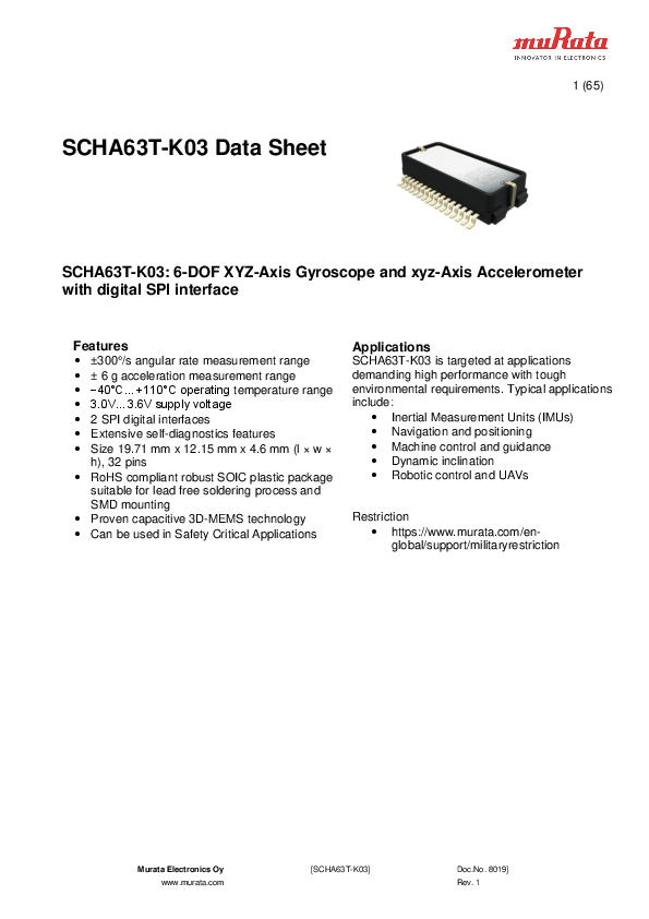
SCHA63T-K03 Data Sheet
2 (65) Murata Electronics Oy [SCHA63T-K03] Doc.No. 8019] www.murata.com Rev. 1 Overview The SCHA63T-K03 is a combined high performance 3-axis angular rate and 3-axis accelerometer.
SCHA63T-K03 Data Sheet - Murata Manufacturing
Full PDF Document

If the inline viewer fails, it will open the original document in compatibility mode automatically. You can also open the file directly.
Extracted Text
1 (65)
SCHA63T-K03 Data Sheet

SCHA63T-K03: 6-DOF XYZ-Axis Gyroscope and xyz-Axis Accelerometer with digital SPI interface

Features  �300�/s angular rate measurement range  � 6 g acceleration measurement range  -40�C...+110�C operating temperature range  3.0V...3.6V supply voltage  2 SPI digital interfaces  Extensive self-diagnostics features  Size 19.71 mm x 12.15 mm x 4.6 mm (l � w �
h), 32 pins  RoHS compliant robust SOIC plastic package
suitable for lead free soldering process and SMD mounting  Proven capacitive 3D-MEMS technology  Can be used in Safety Critical Applications

Applications SCHA63T-K03 is targeted at applications demanding high performance with tough environmental requirements. Typical applications include:
 Inertial Measurement Units (IMUs)  Navigation and positioning  Machine control and guidance  Dynamic inclination  Robotic control and UAVs
Restriction  https://www.murata.com/englobal/support/militaryrestriction

Murata Electronics Oy www.murata.com

[SCHA63T-K03]

Doc.No. 8019] Rev. 1

2 (65)
Overview
The SCHA63T-K03 is a combined high performance 3-axis angular rate and 3-axis accelerometer. It consists of X-, Y- and Z-axis angular rate sensors and integrated 3-axis accelerometer based on Murata's proven capacitive 3D-MEMS technology. Signal processing is done with two mixed signal ASICs that provides angular rate via flexible SPI digital interface. Sensor elements and ASIC are packaged to premolded SOIC 32 plastic housing that guarantees reliable operation over product's lifetime.
The SCHA63T-K03 is designed, manufactured and tested for high stability, reliability and quality requirements. Component has extremely stable output over temperature, humidity and vibration. Component has several advanced self-diagnostic features and is suitable for SMD mounting and is compatible with RoHS and ELV directives.

TABLE OF CONTENTS 1 Introduction.................................................................................................................................4 2 Specifications .............................................................................................................................4
2.1 Abbreviations .........................................................................................................................4 2.2 General Specifications ...........................................................................................................5 2.3 Performance Specifications for Gyroscope ............................................................................6 2.4 Performance Specifications for Accelerometer.......................................................................8 2.5 Performance Specification for Temperature Sensor.............................................................10 2.6 Cross-Axis Compensation ...................................................................................................11
2.6.1 Test Mode For Reading Cross-Axis Terms .....................................................................14 2.7 Absolute Maximum Ratings .................................................................................................14 2.8 Pin Description.....................................................................................................................15 2.9 Typical performace characteristics.......................................................................................16
2.9.1 Gyro typical characteristics .............................................................................................17 2.9.2 Acceleration typical characteristics .................................................................................19 2.10 Digital I/O Specification........................................................................................................21 2.11 Measurement Axis and Directions........................................................................................25 2.12 Package Characteristics ......................................................................................................26 2.12.1 Package Outline Drawing ............................................................................................26 2.13 PCB Footprint ......................................................................................................................27 3 General Product Description....................................................................................................28 3.1 Component block diagram ...................................................................................................28 3.2 Acceleration sensing element ..............................................................................................29 3.3 Angular rate sensing element ..............................................................................................29

Murata Electronics Oy www.murata.com

[SCHA63T-K03]

Doc.No. 8019] Rev. 1

3 (65)

3.4 Factory Calibration...............................................................................................................29 4 Component Operation, Reset and Power Up ..........................................................................30
4.1 Component Operation..........................................................................................................30 4.2 Internal Failsafe Diagnostics ................................................................................................30 5 Component Interfacing.............................................................................................................32 5.1 SPI Interface........................................................................................................................32
5.1.1 General...........................................................................................................................32 5.1.2 Protocol ..........................................................................................................................32 5.1.3 General Instruction format ..............................................................................................33 5.1.4 Operations ......................................................................................................................35 5.1.5 Return Status..................................................................................................................35 5.1.6 Checksum (CRC)............................................................................................................37 6 Register Definition ....................................................................................................................38 6.1 Sensor Data Block ...............................................................................................................39 6.1.1 Example of Angular Rate Data Conversion.....................................................................39 6.1.2 Example of Acceleration Data Conversion ......................................................................39 6.1.3 Example of Temperature Data Conversion .....................................................................40 6.2 Sensor Status Block and Control .........................................................................................40 6.2.1 Summary Status Register (0Eh) .....................................................................................41 6.2.2 Safe Control Register (0Fh) ............................................................................................42 6.2.3 Rate Status 1 Register (10h) ..........................................................................................44 6.2.4 Rate Status 2 Register (11h) ..........................................................................................45 6.2.5 Accelerometer Status 1 Register (12h) ...........................................................................46 6.2.6 Common Status 1 Register (14h)....................................................................................47 6.2.7 Common Status 2 Register (15h)....................................................................................48 6.2.8 Gyro filter control (16h) ...................................................................................................49 6.2.9 SYS_TEST Register (17h)..............................................................................................51 6.2.10 Reset Control Register (18h) .......................................................................................51 6.2.11 Mode Register (19h)....................................................................................................53 6.2.12 ACC filter control (1Ah)................................................................................................55 6.2.13 Component ID Register (1Bh) .....................................................................................57 6.2.14 Traceability 2 Register (1Ch) .......................................................................................57 6.2.15 Traceability 0 Register (1Dh) .......................................................................................57 6.2.16 Traceability 1 Register (1Eh) .......................................................................................57 7 Application information............................................................................................................59 7.1 Application Circuitry and External Component Characteristics.............................................59 7.2 General Application PCB layout ...........................................................................................61

Murata Electronics Oy www.murata.com

[SCHA63T-K03]

Doc.No. 8019] Rev. 1

4 (65)
8 Assembly Instructions..............................................................................................................62 9 Known Bugs..............................................................................................................................62 10 Electrical and mechanical robustness ....................................................................................63 10.1SPI Crosstalk Optimization ......................................................................................................63

1 Introduction
This document contains essential technical information about SCHA63T-K03 sensor including specifications, SPI interface descriptions, user accessible register details, electrical properties and application information. This document should be used as a reference when designing in SCHA63T-K03 component.

2 Specifications
2.1 Abbreviations
ASIC CCM Cpk CSB CST DPS DUE FFB FS HPC MOSI MISO MCU RT SCK SPI UNO F_prim Rx Ry Rz Ax Ay Az

Application Specific Integrated Circuit Channel calibration and monitoring Process Capability Index Chip Select Continuous Self Test Degrees per second ASIC for ZY-axis rate Force Feedback (Gyro operating principle) Full scale High Performance Combo Master Out Slave In Master In Slave Out Microcontroller Room Temperature Serial Clock Serial Peripheral Interface ASIC for X-axis rate and XYZ-axis accelerometer Gyro primary frequency Rate X axis Rate Y axis Rate Z axis Accelerometer X axis Accelerometer Y axis Accelerometer Z axis

Murata Electronics Oy www.murata.com

[SCHA63T-K03]

Doc.No. 8019] Rev. 1

5 (65)

2.2 General Specifications
General specifications for SCHA63T-K03 component are presented in Table 1. All analog voltages are related to the potential at GNDA and all digital voltages are related to the potential at GNDD.

Table 1. General specifications.

Parameter Supply voltage: V3p3A Supply voltage: V3p3D Supply current: V3p3A DUE Supply current: V3p3D DUE Supply current: V3p3A+D DUE Supply current: V3p3A UNO Supply current: V3p3D UNO Supply current: V3p3A+D UNO Total current, I_TOTAL UNO+DUE Total current reset UNO+DUE Output update rate
TMODE
TSPIR

Condition
I_V3p3A + I_V3p3D Temperature range -40 ... +110 �C Total average current during reset Gyro, Accelerometer and Temperature sensor Wait time to set the operation mode after the supply in the specification. Wait time needed after power on or after reset. (Wait time starts when supply is inside spec limits.) SPI is not functional during this time. SPI communication is not allowed for 2ms after SPI Hardreset.

SC/CC CC

Min Typ Max Unit 3.0 3.3 3.6 V 3.0 3.3 3.6 V

8.5

mA

9.5

mA

18

mA

6.25

mA

6.25

mA

12.5

mA

30.5

mA

4 mA

F_prim /2

Hz

25

ms

2

ms

Murata Electronics Oy www.murata.com

[SCHA63T-K03]

Doc.No. 8019] Rev. 1

6 (65)

2.3 Performance Specifications for Gyroscope
Table 2. Gyro performance specifications (VDD = 3.3 V and at room temperature unless otherwise specified). Below values are from device Product and Process Validation (PV) phase unless otherwise specified.

Parameter Measurement range Offset A) Offset temperature dependency B) Offset change over lifetime C) Sensitivity D) Sensitivity temperature dependency E) Sensitivity change over lifetime F) Linearity error G) Noise density Angle Random Walk Bias Instability H) I) J) Orthogonality error Amplitude response -3 dB frequency
Power on start-up time k)
F_prim

Condition
Minimum saturation flag

Axis
XYZ

Offset after calibration, 3

XYZ

N > 234

-40�C  T  +110�C, 3

XY

N = 234

Z

1000 hours of high temperature operating

XY

life (HTOL) at 125�C, VDD=3.6V

N = 234

Z

Sensitivity after calibration at �300�/s, 3

XYZ

N > 90

-40�C  T  +110�C, 3

XY

N = 234 Z

1000 hours of high temperature operating

XY

life (HTOL) at 125�C, VDD=3.6V

N = 234

Z

End point fit to �300 �/s

XYZ

N = 12

3, N = 12

XYZ

3, N = 12

XYZ

At RT, Allan Variance minimum divided by

XYZ

0.664, 3, N = 12

Axis to axis after external cross axis

XYZ

compensation, 3, N = 234

13 Hz Filter, 3, N = 15

XYZ

20 Hz Filter, 3, N = 15

46 Hz Filter, 3, N = 15

300 Hz Filter, 3, N = 15

13 Hz filter (after SPI power on command),

XYZ

MAX

20 Hz filter (after SPI power on command),

MAX

46 Hz filter (after SPI power on command),

MAX

300 Hz filter (after SPI power on command),

MAX

Nominal operation frequency of the sensor

XY

element. All ASIC internal clocks are derived

from a multiple of this frequency

Z

Output update rate

XYZ

G sensitivity(1g x,y,z axis For DC gravity input, 3, N = 48

XYZ

static)

Min Typ � 300

Max

Unit

�/s

-0.8

0

0.8 �/s

-0.65 -0.085 -0.22 -0.06
79 -0.2
0 -0.75 -0.21

80
0.15 0.0015
0.09

0.65 0.085 0.22 0.06
81 0.6 0.2 0.75 0.21 0.25 0.0019 0.11

�/s �/s �/s �/s LSB/�/s % % % % �/s �/s/ �/

1.64 -0.25

2.57 �/h 0.25 %

12.1

13.6

14.3 Hz

18.5

20.2

21.5 Hz

42.1

46.1

48.9 Hz

280

305.8

325.6 Hz

620 ms

620 ms

500 ms

500 ms

15.8

16.8

17.8 kHz

18.3

19.3

20.3 kHz

F_prim/2

0.006 (�/s)/g

Murata Electronics Oy www.murata.com

[SCHA63T-K03]

Doc.No. 8019] Rev. 1

7 (65)
A) Initial offset at Murata Production measurement after calibration B) Offset temperature dependency is determined by the larger absolute value of [(maximum offset over temperature) � (offset at 25�C)] or
[(minimum offset over temperature) � (offset at 25�C)] C) Estimated from offset change during 1000 hours of high temperature operating live (HTOL) test at 125�C and maximum supply voltages D) Sensitivity is defined as
    Sensitivity  ARmeas max  ARmeas min
max  min
Where max=applied angular rate at maximum operating range min=applied angular rate at minimum operating range ARmeas(n)=measured angular rate at n [LSB]
E) Sensitivity temperature dependency is determined by the larger absolute value of [(maximum sensitivity value over temperature) - (sensitivity at 25C)] /sensitivity at 25C*100% or [(minimum sensitivity value over temperature) - (sensitivity at 25C)] /sensitivity at 25C*100%
F) Estimated from sensitivity change during 1000 hours of high temperature operating life (HTOL) test at 125�C and maximum supply voltages G) Linearity is the maximum deviation from the straight line defined by the measured values at the operating range end points. H) Allan Variance Minimum divided by 0.664

I) Optimization for SPI duty cycle or sample rate is required to achieve typical Allan variance in table J) Device powered four hours before data collection starts to permit fully settling from power up. K) Max values are determined from product platform validations

Note :

�

Specification is valid after 24hours from reflow.

�

Each system design including SCHA63T-K03 must be evaluated by the customer in advance to guarantee proper functionality during operation.

�

Min and Max values are from validation mean �3 sigma variation limits from test population at the minimum. Min and Max values are not

guaranteed. Nominal values are mean values from validation test population.

Murata Electronics Oy www.murata.com

[SCHA63T-K03]

Doc.No. 8019] Rev. 1

8 (65)

2.4 Performance Specifications for Accelerometer
Table 3. Accelerometer performance specifications (VDD = 3.3 V and room temperature unless otherwise specified). Below values are from device Product and Process Validation (PV) phase unless otherwise specified.

Parameter

Condition

Measurement range Offset A) Offset temperature dependency B) Offset change over lifetime C)
Sensitivity D) Sensitivity temperature dependency E) Sensitivity change over lifetime F)
Linearity error G)
Noise density

Minimum saturation flag
Offset after calibration, 3 N = 234 -40�C  T  +110�C, 3 N = 234
1000 hours of high temperature operating life (HTOL) at 125�C, VDD=3.6V N = 234 Sensitivity after calibration at �1g, 3 N = 234 -40�C  T  +110�C, 3 N = 234
1000 hours of high temperature operating life (HTOL) at 125�C, VDD=3.6V N = 234 End point fit to �6g 3, N = 30 End point fit to �1g 3, N = 30 3, N = 12

Velocity random walk Bias instability
Orthogonality error Amplitude response -3 dB frequency

3, N = 12
At RT, Allan Variance minimum divided by 0.664, 3, N = 12 Axis to axis after external cross axis compensation, 3, N = 234 13 Hz Filter, 3, N = 15
20 Hz Filter, 3, N = 15

46 Hz Filter, 3, N = 15

300 Hz Filter, 3, N = 15

Power on start-up time
H)
Output update rate

13 Hz filter (after SPI power on command) , MAX 20 Hz filter (after SPI power on command) , MAX 46 Hz filter (after SPI power on command) , MAX 300 Hz filter (after SPI power on command) , MAX Tied to X-gyro F_prim/2

Axis
XYZ XYZ XYZ XYZ
XYZ XYZ XYZ
XYZ XYZ XYZ XYZ XYZ XYZ XYZ XYZ XYZ XYZ XYZ
XYZ

Min 6
-13.5 -7.3 -22 4899 -0.15 -0.06 1.9
-0.14 13.2 19.7 45.0 247.4
7.9

Typ
4905
6.3 59.5 35.0 12.2 13.7 20.3 46.3 264.2
8.4

Max
13.5 7.3 22
4911 0.15 0.06
17.2 1
66.0 38.8 18.3 0.14 14.2 20.8 47.5 286.7 450 450 320 320 8.9

Unit g mg mg
mg
LSB/g %
%
mg mg g/ mm/s / g % Hz Hz Hz Hz ms ms ms ms kHz

Murata Electronics Oy www.murata.com

[SCHA63T-K03]

Doc.No. 8019] Rev. 1

9 (65)

A) Initial offset at Murata Production measurement after calibration B) Offset temperature dependency is determined by the larger absolute value of [(maximum offset over temperature) � (offset at 25�C)] or
[(minimum offset over temperature) � (offset at 25�C)] C) Estimated from offset change during 1000 hours of high temperature operating life (HTOL) test at 125�C D) Sensitivity is defined as
    Sensitivity  ACCmeas a1g  ACCmeas a1g a1g  a1g
Where a+1g=applied acceleration at +1g a-1g=applied acceleration at -1g ACCmeas(an)=measured acceleration at an [LSB]
E) Sensitivity temperature dependency is determined by the larger absolute value of [(maximum sensitivity value over temperature) - (sensitivity at 25C)] /sensitivity at 25C*100% or [(minimum sensitivity value over temperature) - (sensitivity at 25C)] /sensitivity at 25C*100%
F) Estimated from Sensitivity change during 1000 hours of high temperature operating life (HTOL) test at 125�C G) Linearity is the maximum deviation from the straight line defined by the measured values at the specified range end points. H) Max values are determined from product platform validations

Note :

�

Specification is valid after 24hours from reflow.

�

Each system design including SCHA63T-K03 must be evaluated by the customer in advance to guarantee proper functionality during operation.

�

Min and Max values are validation �3 sigma variation limits from test population at the minimum. Min and Max values are not guaranteed. Nominal

values are mean values from validation test population.

Murata Electronics Oy www.murata.com

[SCHA63T-K03]

Doc.No. 8019] Rev. 1

10 (65)

2.5 Performance Specification for Temperature Sensor

Table 4. Temperature sensor performance specifications.

Parameter Temperature signal range Temperature signal sensitivity

Condition
Temperature sensor output in 2's complement format

Min. Typ Max. Unit

-50

+150 �C

30

LSB/�C

Temperature is converted to �C with following equation:

Temperature [�C] = 25 + (TEMP / 30),

where TEMP is temperature sensor output register content in decimal format.

Murata Electronics Oy www.murata.com

[SCHA63T-K03]

Doc.No. 8019] Rev. 1

11 (65) 2.6 Cross-Axis Compensation
SCHA63T-K03 ASIC stores the cross-axis compensation and offset fine tuning terms both for the rate and accelerometer and cross-axis compensation can be done in the external microprocessor according to the following equations.
Equation 1: Rate Cross-Axis Compensation
where cii = is the corresponding rate cross-axis compensation term (in non-volatile memory,
see Table 5: Cross-Axis Compensation Register Map)
Equation 2: Compensated rate vector
Equation 3: Measured rate vector (from the component)
Equation 4: Rate offset compensation vector (Not stored in the memory). Rate offset zeroing in system level e.g. after PCB assembly is recommended.

Murata Electronics Oy www.murata.com

[SCHA63T-K03]

Doc.No. 8019] Rev. 1

For the accelerometers following equations apply:
Equation 5: Accelerometer Cross-Axis Compensation

12 (65)

where bii = is the corresponding accelerometer cross-axis compensation term (see Table 5:
Cross-Axis Compensation Register Map)
Equation 6: Compensated accelerometer vector
Equation 7: Measured accelerometer vector (from the component)

Equation 8: Acceleration offset compensation vector (Not stored in the memory). Acceleration offset zeroing in system level e.g. after PCB assembly is recommended.

Note: Sensing element axes are independent from each other by the mechanical design. The cross-axis compensation doesn't affect to axis independency as long as no axes are saturated.

Murata Electronics Oy www.murata.com

[SCHA63T-K03]

Doc.No. 8019] Rev. 1

13 (65)

Table 5: Cross-Axis Compensation Register Map

Parameter
cxx cxy cxz cyx cyy cyz czx czy czz bxx bxy bxz byx byy byz bzx bzy bzz

Bank (DUE ASIC) 05h 05h 05h 05h 05h 05h 05h 05h 05h 05h 05h 05h 05h 05h 05h 05h 05h 05h

Addre ss (hex) 0Bh 0Bh 13h 13h 14h 14h 15h 15h 16h 16h 17h 17h 18h 18h 1Bh 1Bh 1Ch 1Ch

Register
ACC_DC1[7:0] ACC_DC1[15:8] ACC_DC9[7:0] ACC_DC9[15:8] ACC_DC10[7:0] ACC_DC10[15:8] ACC_DC11[7:0] ACC_DC11[15:8] ACC_DC12[7:0] ACC_DC12[15:8] ACC_DC13[7:0] ACC_DC13[15:8] ACC_DC14[7:0] ACC_DC14[15:8] ACC_MD1[7:0] ACC_MD1[15:8] ACC_MD2[7:0] ACC_MD2[15:8]

Range (2's complement)
- 128 .. 127 LSB - 128 .. 127 LSB - 128 .. 127 LSB - 128 .. 127 LSB - 128 .. 127 LSB - 128 .. 127 LSB - 128 .. 127 LSB - 128 .. 127 LSB - 128 .. 127 LSB - 128 .. 127 LSB - 128 .. 127 LSB - 128 .. 127 LSB - 128 .. 127 LSB - 128 .. 127 LSB - 128 .. 127 LSB - 128 .. 127 LSB - 128 .. 127 LSB - 128 .. 127 LSB

Floating number
1+value/4096 value/4096 value/4096 value/4096 1+value/4096 value/4096 value/4096 value/4096 1+value/4096 1+value/4096 value/4096 value/4096 value/4096 1+value/4096 value/4096 value/4096 value/4096 1+value/4096

Murata Electronics Oy www.murata.com

[SCHA63T-K03]

Doc.No. 8019] Rev. 1

14 (65)

2.6.1 Test Mode For Reading Cross-Axis Terms
Procedure 1) Activate test mode (open lock) after Step 3 (or 4 or 5 or 6) of start-up sequence in Figure 7
 Write/Read Register 19h (Mode) o Write Mode='RRRRRRRR RR010RRR'b o Read Mode o Write Mode='RRRRRRRR RR001RRR'b o Read Mode o Write Mode='RRRRRRRR RR100RRR'b o Read Mode o Dummy read, for example read Mode to get Mode read response
 Verify test mode o Check the read data bits Mode[2:0]='111'b
2) Change bank to 5  Write data 5'h to address 1F'h
3) Read cross-axis terms  Read registers according to Table 5
4) Save cross-axis terms to MCU 5) Power-off or SPI reset command via register 18h or reset by EXTRESN pin to exit test mode 6) Return to Step 1 of start-up sequence in Figure 7
*Write operation to an unspecified register after test mode access may permanently damage the component.
2.7 Absolute Maximum Ratings
Within the maximum ratings (Table 6. Absolute maximum ratings.), no damage to the component shall occur. Parametric values may deviate from specification, yet no functional deviation shall occur. All analog voltages are related to the potential at GNDA, all digital voltages are related to GNDD.

Table 6. Absolute maximum ratings.

Parameter Remark

Min.

Typ

Max.

Unit

VDD

Supply voltage

-0.3

4.3

V

AIN/AOUT Maximum voltage at analog input and output pins

-0.3

VDD+0.3 (4.3)

V

DIN/DOUT Maximum voltage at digital input and output pins

-0.3

VDD+0.3 (4.3)

V

Topr

Operating temperature range

-40

110

�C

Tstg

Storage temperature range

-40

150

�C

ESD_HBM ESD according Human Body Model (HBM), Q100-002

�2000

V

ESD_MM ESD according Machine Model (MM), Q100-003

�200

V

ESD_CDM ESD according Charged Device Model (CDM),

�500

Q100-011

�750 (corner

V

pins)

US

Ultrasonic agitation (cleaning, welding, etc)

Prohibited

Murata Electronics Oy www.murata.com

[SCHA63T-K03]

Doc.No. 8019] Rev. 1

15 (65)
2.8 Pin Description The pinout for SCHA63T-K03 is presented in Figure 1, while the pin descriptions can be found in Table 7.

Figure 1. Pinout for SCHA63T-K03.

Murata Electronics Oy www.murata.com

[SCHA63T-K03]

Doc.No. 8019] Rev. 1

16 (65)

Table 7. SCHA63T-K03 pin descriptions.

Pin# 1 2 3 4 5 6 7 8

Name HEAT/EMC_GND
MOSI CSB SCK MISO V3p3D V3p3A GNDD

ASIC -
DUE DUE DUE DUE DUE DUE DUE

9

VDDD

DUE

10 GNDA / EMC_GND UNO

11

VDDA

UNO

12

RESERVED

UNO

13

TIOP

UNO

14

TI/EXTRESN

UNO

15

TION

UNO

16 HEAT/EMC_GND -

17 HEAT/EMC_GND -

18

MOSI

UNO

19

CSB

UNO

20

SCK

UNO

21

MISO

UNO

22

V3p3D

UNO

23

V3p3A

UNO

24

GNDD

UNO

25

VDDD

UNO

26 GNDA / EMC_GND DUE

27

VDDA

DUE

28

RESERVED

DUE

29

TIOP

DUE

30

TI/EXTRESN

DUE

31

TION

DUE

32 HEAT/EMC_GND -

Type Description

GND Heatsink interface to GNDA

DIN Data In of SPI Interface

DIN Chip Selected of SPI Interface

DIN Clock Signal of SPI Interface

DOUT Data Out of SPI Interface

SUPPLY Digital Supply voltage

SUPPLY Analog Supply voltage

GND Digital Supply return (ground), connect externally to GNDA.

AOUT

Regulated supply for digital core. Use external capacitor which is connected according to the diagram in Figure 15.

GND Analog Supply return (ground), connect externally to GNDD

AOUT

Regulated supply for analog core. Use external capacitor which is connected according to the diagram in Figure 15.

-

Factory use only, connect to GND

-

Factory use only, connect to GND.

Optional external Reset, 3.3V logic compatible SchmittDIN trigger input with internal pull-up, LOW-HIGH transition
causes system restart. Minimum low time 100us.

-

Factory use only, connect to GND.

GND Heatsink interface to GNDA

GND Heatsink interface to GNDA

DIN Data In of SPI Interface

DIN Chip Selected of SPI Interface

DIN Clock Signal of SPI Interface

DOUT Data Out of SPI Interface

SUPPLY Digital Supply voltage

SUPPLY Analog Supply voltage

GND Digital Supply return (ground), connect externally to GNDA.

AOUT

Regulated supply for digital core. Use external capacitor which is connected according to the diagram in Figure 15.

GND Analog Supply return (ground), connect externally to GNDD

AOUT

Regulated supply for analog core. Use external capacitor which is connected according to the diagram in Figure 15.

-

Factory use only, connect to GND

-

Factory use only, connect to GND.

Optional external Reset, 3.3V logic compatible SchmittDIN trigger input with internal pull-up, LOW-HIGH transition
causes system restart. Minimum low time 100us.

-

Factory use only, connect to GND.

GND EMC protection and ground

2.9 Typical performace characteristics
Murata Electronics Oy www.murata.com

[SCHA63T-K03]

Doc.No. 8019] Rev. 1

2.9.1 Gyro typical characteristics

17 (65)

Chart 1 Gyro Offset Error over temperature X-axis

Chart 2 Gyro Offset Error @ +23�C X-axis

Chart 3 Gyro Offset Error over temperature Y-axis

Chart 4 Gyro Offset Error @ +23�C Y-axis

Chart 5 Gyro Offset Error over temperature Z-axis

Chart 6 Gyro Offset Error @ +23�C Z-axis

Murata Electronics Oy www.murata.com

[SCHA63T-K03]

Doc.No. 8019] Rev. 1

18 (65)

Chart 7 Gyro Sensitivity Error over temperature X-axis

Chart 8 Gyro Sensitivity Error @ +23�C X-axis

Chart 9 Gyro Sensitivity Error over temperature Y-axis

Chart 10 Gyro Sensitivity Error @ +23�C Y-axis

Chart 11 Gyro Sensitivity Error over temperature Z-axis

Chart 12 Gyro Sensitivity Error @ +23�C Z-axis

Chart 13 Gyro Allan Deviation X-,Y, and Z-axis

Murata Electronics Oy www.murata.com

[SCHA63T-K03]

Doc.No. 8019] Rev. 1

2.9.2 Acceleration typical characteristics

19 (65)

Chart 14 Accelerometer offset error over temperature X-axis

Chart 15 Accelerometer Offset Error @ +23�C X-axis

Chart 16 Accelerometer offset error over temperature Y-axis

Chart 17 Accelerometer Offset Error @ +23�C Y-axis

Chart 18 Accelerometer offset error over temperature Z-axis

Chart 19 Accelerometer Offset Error @ +23�C Z-axis

Murata Electronics Oy www.murata.com

[SCHA63T-K03]

Doc.No. 8019] Rev. 1

20 (65)

Chart 20 Accelerometer Sensitivity Error over temperature X-axis

Chart 21 Accelerometer Sensitivity Error @ +23�C X-axis

Chart 22 Accelerometer Sensitivity Error over temperature Y-axis

Chart 23 Accelerometer Sensitivity Error @ 23�C Y-axis

Chart 24 Accelerometer Sensitivity Error over temperature Z-axis

Chart 25 Accelerometer Sensitivity Error @ 23�C Z-axis

Chart 26 Acceleration Allan Deviation X-,Y- and Z-axis

Murata Electronics Oy www.murata.com

[SCHA63T-K03]

Doc.No. 8019] Rev. 1

21 (65)

2.10 Digital I/O Specification
Table 8 describes the DC characteristics of SCHA63T-K03 sensor SPI I/O pins. Supply voltage is 3.3 V unless otherwise specified. Current flowing into the circuit has a positive value.

Table 8. SPI DC characteristics.

Symbol

Description

Serial Clock SCLK

VinHigh

Input high voltage

VinLow

Input low voltage

Vhy

Input hysteresis

Isource

Input current source (Pull down)

Cin

Input capacitance

Min.

Nom.

Max.

Unit

2

V3p3D+0.3 V

-0.3

0.8

V

0.2

V

24

36

uA

6

pF

Chip select CSB (Pull Up), low active

VinHigh

Input high voltage

2

VinLow

Input low voltage

-0.3

Vhy

Input hysteresis

0.2

Isource

Input current source (Pull Up), Vin = 0V

24

Cin

Input capacitance

Vin_open

Open circuit output voltage

2

V3p3D+0.3 V

0.8

V

V

36

uA

6

pF

V

Serial data input MOSI (Pull Down)

VinHigh

Input high voltage

2

VinLow

Input low voltage

-0.3

Vhy

Input hysteresis

0.2

Isource

Input current source (Pull Up), Vin = DVDD

24

Cin

Input capacitance

Vin_open

Open circuit output voltage

V3p3D+0.3 V

0.8

V

V

36

uA

6

pF

0.3

V

Serial data output MISO (Tri state)

VoutHigh_-1mA Output high voltage, Iout = -1mA

VinHigh_1mA Output low voltage, Iout = +1mA

Iout_Hz

High impedance output current, 0V < VMISO < V3p3D

Cld_miso

Capacitive load. The slope of the MISO output signal can be controlled to meet EMI requirements under specified load conditions.

V3p3D-0.5 -1

V

0.5

V

1

uA

200

pF

Table 9. EXTRESN pin characteristics

Symbol

Description

Digital pin EXTRESN

VinHigh

Input high voltage

VinLow

Input low voltage

Vhy

Input hysteresis

Isource

Start-up indication phase inactive Start-up indication phase active

Murata Electronics Oy www.murata.com

[SCHA63T-K03]

Min.

Nom.

Max.

Unit

2

V3p3A+0.3 V

-0.3

0.8

V

0.2

V

60

160

�A

30

80

�A

Doc.No. 8019] Rev. 1

22 (65) 2.11 SPI AC Characteristics
The AC characteristics of SCHA63T-K03 are defined in Figure 2 and Table 10.
Figure 2. Timing diagram of SPI communication. Table 10. SPI AC electrical characteristics.

Murata Electronics Oy www.murata.com

[SCHA63T-K03]

Doc.No. 8019] Rev. 1

23 (65)

Symbol

Description

Min.

fSPI

Master (MCU): SPI SCLK frequency

0.1

tSPI

Master (MCU): SPI SCLK period

-

thigh

Master (MCU):

High time: duration of logical high level at SCLK (from VinHigh_min to

35

VinHigh_min)

Master (MCU):

tlow

Low time: duration of logical low level at SCLK (from VinLow_max to

35

VinLow_max)

Master (MCU): Setup time CSB: time between the tsucs falling edge of CSB and the rising edge 40
of SCLK (from VinLow_max to VinLow_max)

tsusi

Master (MCU): Setup time at MOSI: setup time of MOSI before the rising edge of SCLK 10 (from VinLow_max to VinLow_max or from VinHigh_min to VinLow_max)

Master(MCU):

Hold time at MOSI: hold time of MOSI

thsi

after rising edge of SCLK (from

20

VinHigh_min to VinLow_max or to

VinHigh_min)

Master (MCU):

Hold time of CSB: time between the

thcs

falling edge of SCLK and the rising

30

edge of CSB (from VinLow_max to

VinLow_max)

thics

Master (MCU):

Minimum high time of CSB between two consecutive transfers (from

30

VinHigh_min to VinHigh_min)

Master (MCU):

trise/fall_in

Rise/fall time of SCK/MOSI signals (from VinLow_max to VinHigh_min or

-

from VinHigh_min to VinLow_max)

Slave(=SCHA63T-K03 ASIC):

Delay time: time delay from the falling

td1

edge of CSB to data valid at MISO

-

(from VinLow_max to VInLow_max or

to VInHigh_min)

Nom. -
1/ fSPI tSPI/2 tSPI/2 tSPI/2
-
-
tSPI/2 tSPI/2
-

Max. 10 -

Unit MHz
-

-

ns

-

ns

-

ns

-

ns

-

ns

-

ns

ns

0.15x tSPI

ns

30

ns

Murata Electronics Oy www.murata.com

[SCHA63T-K03]

Doc.No. 8019] Rev. 1

24 (65)

Slave(=SCHA63T-K03 ASIC):

Delay time: time delay from falling edge

td2

of SCLK to data valid at MISO (from

0

-

30

ns

VinLow_max to VInLow_max or to

VInHigh_min)

Slave(=SCHA63T-K03 ASIC):

ttri

Tri-state delay time: time between the rising edge of CSB to MISO in Tri-state

-

(from VinHigh_min to X)

-

25

ns

Slave(=SCHA63T-K03 ASIC): Rise/fall

time of MISO signal (VOut_10% to

trise/fall_out

VOut_90% and from VOut_90% to VOut_10%)

4

10

16

ns

User selectable MISO slew rate control

in Mode register (19h)

Murata Electronics Oy www.murata.com

[SCHA63T-K03]

Doc.No. 8019] Rev. 1

2.12 Measurement Axis and Directions

25 (65)

Figure 3. SCHA63T-K03 measurement directions. Table 11 SCHA63T-K03 accelerometer measurement directions and outputs

Murata Electronics Oy www.murata.com

[SCHA63T-K03]

Doc.No. 8019] Rev. 1

26 (65)
2.13 Package Characteristics 2.13.1 Package Outline Drawing
The SCHA63T-K03 package outline and dimensions are presented in The outline of the SCHA63T-K03 package (SOIC-32) in mm. and Table 12. Limits for linear measures (ISO2768-f) unless tolerance is not specified in Figure 4 The outline of the SCHA63TK03 package (SOIC-32) in mm.

Figure 4 The outline of the SCHA63T-K03 package (SOIC-32) in mm.

Table 12. Limits for linear measures (ISO2768-f) unless tolerance is not specified in Figure 4 The outline of the SCHA63T-K03 package (SOIC-32) in mm.

Tolerance class Limits in mm for nominal size in mm

0.5 to 3

Above 3 to 6

Above 6 to 30 Above 30 to 120

f (fine)

�0.05

�0.05

�0.1

�0.15

It is not applicable for number shown in table of center point of the sensor element in figure 4, which is only for reference.

Murata Electronics Oy www.murata.com

[SCHA63T-K03]

Doc.No. 8019] Rev. 1

27 (65)
2.14 PCB Footprint SCHA63T-K03 footprint dimensions are presented in Figure 5. Recommended PWB pad layout for SCHA63T-K03.

Figure 5. Recommended PWB pad layout for SCHA63T-K03.

Murata Electronics Oy www.murata.com

[SCHA63T-K03]

Doc.No. 8019] Rev. 1