AD9081/AD9082 Software Development User Guide, UG-1578 (Rev. 0)
File info: application/pdf · 315 pages · 7.74MB
AD9081/AD9082 Software Development User Guide, UG-1578 (Rev. 0)
high speed adc, mixed signal front ends, AD9081, AD9986, AD9988, AD9082, TxFE, MxFE, AD9177, AD9209, AD9207
"high speed adc, mixed signal front ends, AD9081, AD9986, AD9988, AD9082, TxFE, MxFE, AD9177, AD9209, AD9207"
Extracted Text
AD9081/AD9082 System Development User Guide
UG-1578
One Technology Way � P.O. Box 9106 � Norwood, MA 02062-9106, U.S.A. � Tel: 781.329.4700 � Fax: 781.461.3113 � www.analog.com
AD9081 and AD9082 Direct RF Sampling Transceivers
SCOPE
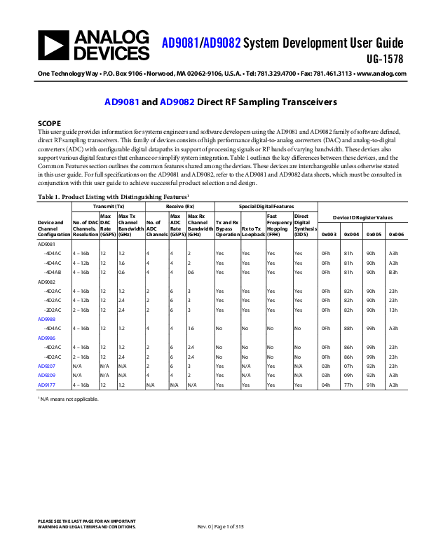
This user guide provides information for systems engineers and software developers using the AD9081 and AD9082 family of software defined, direct RF sampling transceivers. This family of devices consists of high performance digital-to-analog converters (DAC) and analog-to-digital converters (ADC) with configurable digital datapaths in support of processing signals or RF bands of varying bandwidth. These devices also support various digital features that enhance or simplify system integration. Table 1 outlines the key differences between these devices, and the Common Features section outlines the common features shared among the devices. These devices are interchangeable unless otherwise stated in this user guide. For full specifications on the AD9081 and AD9082, refer to the AD9081 and AD9082 data sheets, which must be consulted in conjunction with this user guide to achieve successful product selection and design.
Table 1. Product Listing with Distinguishing Features1
Transmit (Tx)
Receive (Rx)
Special Digital Features
Max Max Tx
Max Max Rx
Fast
Direct
Device and No. of DAC DAC Channel No. of ADC Channel Tx and Rx
Frequency Digital
Channel
Channels, Rate Bandwidth ADC
Rate Bandwidth Bypass Rx to Tx Hopping Synthesis
Configuration Resolution (GSPS) (GHz)
Channels (GSPS) (GHz)
Operation Loopback (FFH)
(DDS)
Device ID Register Values 0x003 0x004 0x005 0x006
AD9081
-4D4AC 4 � 16b 12 1.2
4
4
2
Yes
Yes
Yes
Yes
0Fh
81h
90h
A3h
-4D4AC 4 � 12b 12 1.6
4
4
2
Yes
Yes
Yes
Yes
0Fh
81h
90h
A3h
-4D4AB 4 � 16b 12 0.6
4
4
0.6
Yes
Yes
Yes
Yes
0Fh
81h
90h
B3h
AD9082
-4D2AC 4 � 16b 12 1.2
2
6
3
Yes
Yes
Yes
Yes
0Fh
82h
90h
23h
-4D2AC 4 � 12b 12 2.4
2
6
3
Yes
Yes
Yes
Yes
0Fh
82h
90h
23h
-2D2AC 2 � 16b 12 2.4
2
6
3
Yes
Yes
Yes
Yes
0Fh
82h
90h
13h
AD9988
-4D4AC 4 � 16b 12 1.2
4
4
1.6
No
No
No
No
0Fh
88h
99h
A3h
AD9986
-4D2AC 4 � 16b 12 1.2
2
6
2.4
No
No
No
No
0Fh
86h
99h
23h
-4D2AC 2 � 16b 12 2.4
2
6
2.4
No
No
No
No
0Fh
86h
99h
23h
AD9207
N/A
N/A N/A
2
6
3
Yes
N/A
Yes
N/A
03h
07h
92h
23h
AD9209
N/A
N/A N/A
4
4
2
Yes
N/A
Yes
N/A
03h
09h
92h
A3h
AD9177
4 � 16b 12 1.2
N/A
N/A N/A
Yes
Yes
Yes
Yes
04h
77h
91h
A3h
1 N/A means not applicable.
PLEASE SEE THE LAST PAGE FOR AN IMPORTANT WARNING AND LEGAL TERMS AND CONDITIONS.
Rev. 0 | Page 1 of 315
UG-1578
AD9081/AD9082 System Development User Guide
TABLE OF CONTENTS
Scope .............................................................................................. 1
SYSREF Modes ....................................................................... 28
System Overview .............................................................................. 6
SYSREF Monitor Mode......................................................... 28
Common Features........................................................................ 6
SYSREF Error Window......................................................... 28
Analog Features........................................................................ 6
SYSREF Sampling Modes ..................................................... 29
Digital Features......................................................................... 6
SYSREF Setup/Sync Procedure ............................................ 30
SERDES Interface..................................................................... 6
SYSREF Phase Adjust ............................................................ 31
Software Overview............................................................................ 9
SYSREF Configuration APIs ................................................ 31
Software Architecture .................................................................. 9
Receive Input and Digital Datapath ............................................ 34
Folder Structure............................................................................ 9
ADC Architecture Overview .................................................... 34
/src/ad9081_api ........................................................................ 9
Calibration and Specifying Nyquist Zone .......................... 34
/src/ad9081_api/adi_inc.......................................................... 9
ADC Input Buffer ...................................................................... 35
/src/ad9081_api/adi_utils........................................................ 9
ADC Input Buffer API .......................................................... 36
/src/ad9081_api/ad9081 .......................................................... 9
Overload Protection .............................................................. 36
/src/ad9081_app ..................................................................... 10
ADC Input Driving Considerations.................................... 37
/doc........................................................................................... 10
Receive Digital Datapath Overview......................................... 38
API Integration and Build......................................................... 10
Receive Data Path Configuration Considerations ................ 39
Integrating the AD9xxx API Into an Application ............. 10
Receive Datapath Configuration API ................................. 40
API Overview Block Diagram .................................................. 12
Mux0 ............................................................................................ 40
Serial Peripheral Interface ............................................................. 14
MUX0 Configuration API .................................................... 41
SPI Configuration API .............................................................. 14
Bypassable Integer Delay and PFILT ...................................... 41
Sampling Clock and Distribution Options ................................. 16
Integer Delay and PFILT Configuration API .................... 42
Clock Multiplier ......................................................................... 16
Mux1 ............................................................................................ 42
Clock Receiver Input ................................................................. 18
Mux1 Configuration API...................................................... 42
Clock Output Driver .................................................................. 20
Receive Main Digital Datapath ................................................ 43
Clock Configuration APIs......................................................... 20
Main Data Path CDDC ......................................................... 43
JESD204B/C Interface Functional Overview and Common Requirements ................................................................................... 21
New Features in the JESD204C Standard ............................... 21
Terminology and Parameters ............................................... 21
CDDC Variable IF NCO Operating Modes....................... 45
CDDC NCO Synchronization Options .............................. 46
NCO Setting Consideration for Homodyne Transmit-toReceive Loopback Applications. .......................................... 47
Physical Layer Updates.......................................................... 22
NCO Dual Modulus Mode ................................................... 47
Transport and Link Layer ..................................................... 22
NCO Integer-N Mode ........................................................... 48
Multiblocks (MB) and Extended Multiblocks (EMB) ...... 22 Synchronization Word .......................................................... 24 CRC-12 Encoder .................................................................... 24 8-Bit/10-Bit Link Establishment Overview ............................ 24 64-Bit/66-Bit Link Establishment Overview .......................... 24 SERDES PLL and Configuration.............................................. 24 SERDES PLL Configuration API ......................................... 25 SYSREF and Subclass 1 Operation .......................................... 26 SYSREF Receiver Input and Interface Options ................. 27
Optional Fractional Delay for Receive Main Datapath 0 or Receive Main Datapath 3 Only ............................................ 48 Main Datapath Decimation Stage ....................................... 49 Bypassable 6 dB Gain Stage and Complex to Real Conversion.............................................................................. 49 Mux2 ........................................................................................ 50 Receive Channelizer Digital Datapath .................................... 51 Receive Channelizer Fine Digital Downconverter............ 51 FDDC Variable IF NCO Operating Modes ....................... 51 NCO Synchronization Options for FDDC ........................ 53
Rev. 0 | Page 2 of 315
AD9081/AD9082 System Development User Guide
UG-1578
NCO Dual Modulus Mode for FDDC .................................53 NCO Integer-N Mode for FDDC .........................................53 Receive Channelizer Decimation Stage ...............................53 Bypassable 6 dB Gain Stage and C2R Conversion .............54 Upsampler................................................................................55 MUX3 (Data Format and Selection)....................................55 Mux4 (JESD204B/C Transmitter JESD Data Router) .........56 JESD204B/C Transmitter...........................................................57 Functional Overview ..............................................................57 JESD204B/C Transmitter Clock Relationships ..................58 Transport Layer.......................................................................58 Data Link Layer Selection, Selecting the Encode Scheme.58 8-Bit/10-Bit Link Layer ..........................................................58 64-Bit/66-Bit Link Layer and Link Establishment .............60 JESD204B/C Transmitter Physical Layer ............................61 ADC Path Deterministic Latency.........................................66 JESD204B/C Transmitter Multichip Synchronization......68 Configuring the JESD204B/C Transmitter Link ....................69 High Level Configuration Process........................................69 JESD204B/C Transmitter Configuration API ....................69 JESD204B/C Transmitter Mode Tables...............................76 Transmit Digital Data Path and Output ................................... 111 JESD204B/C Receiver Functional Overview........................ 111 JESD204B/C Receiver Clock Relationships ..................... 111 Physical Layer ....................................................................... 111 Data Link Layer.................................................................... 114 JESD204C Receiver 64-bit/66-bit Link Layer .................. 123 DAC Path Deterministic Latency...................................... 125 JESD204B/C Receiver Multichip Synchronization ......... 128 JESD204B/C Receiver Transport Layer ............................ 129 JESD204B/C Receive Mode Tables ................................... 129 Configuring the JESD204B/C Receiver ................................ 132 High Level Configuration Process..................................... 132 JESD204B/C Receiver Configuration API ....................... 132 Transmit Path and JESD204B/C Receiver API Functions ................................................................................................ 133 Transmit Digital Datapath Overview.................................... 134 Total Datapath Interpolation ............................................. 135 Data Router Multiplexers and Default Mapping................. 136 4 � 4 Crossbar....................................................................... 136 Channelizer Data Path ............................................................ 137
Digital Gain ...........................................................................137 Skew Adjust ...........................................................................138 Channelizer Interpolation Stage.........................................138 Channelizer FDUC...............................................................138 FDUC Dual Modulus NCO Mode .....................................139 Channelizer NCO Only Mode............................................140 8 � 8 Crossbar Multiplexer......................................................140 Main Digital Datapath .............................................................141 Digital Gain Scaling..............................................................142 Main Datapath Interpolation Stage ...................................142 Main Datapath CDUC.........................................................143 CDUC NCO Synchronization and Reset ..........................144 CDUC Dual-Modulus NCO Mode....................................144 CDUC Integer NCO Mode and Phase Offset...................144 Main Path NCO Only Mode...............................................144 Optional Calibration NCO..................................................144 Modulator Multiplexer (Mod Mux) ..................................145 DAC Outputs ............................................................................149 DAC Outputs API ................................................................150 DAC Output Impedance Characteristics ..........................150 DC-Coupled Operation .......................................................151 MSB Shuffle ...........................................................................151 MSB Rotation ........................................................................152 Auxiliary Features.........................................................................153 Receive AGC Assist Functions................................................153 Fast Detect Mode Configuration Examples......................154 Signal Monitor Block ...........................................................155 Programmable Filter (PFILT) .................................................157 Supported Modes in the AD9082 .......................................159 Supported Modes in the AD9081.......................................160 Use Case Scenarios to Filter Modes Mapping ..................161 Programmable Gain Scaling ...............................................161 Coefficient Bank Description and Fast Updating Between Coefficient Banks..................................................................162 Coefficient Size Optimizations ...........................................163 SPI Programming of Coefficients.......................................163 Transmit Downstream Power Amplifier Protection...........165 Power Detection and Protection (PDP) Block .................166 JESD Interface and Synchronization Error Protection ...166 Ramp-Up and Ramp-Down Gain ......................................167 Transmit Power Control..........................................................167
Rev. 0 | Page 3 of 315
UG-1578
AD9081/AD9082 System Development User Guide
IRQ ............................................................................................. 168 Interrupt Service Routine.................................................... 168
GPIOx Pin Operation .............................................................. 168 Temperature Monitoring Unit (TMU) ................................. 171 AD9081/AD9082/AD9177 Only Features ................................ 172 Transmit and Receive Bypass Mode...................................... 172 FFH Mode ................................................................................. 172
Transmit Main Path FFH NCO Mode.............................. 172 Receive Main and Channelizer Path FFH NCO Mode... 173 Receive to Transmit Analog Loopback ................................. 176 Applications Information............................................................ 178 Device Latency .......................................................................... 178 Receive Path End to End Total Latency ............................ 178 System Multichip Synchronization ....................................... 179 Quad MxFE Reference Design ........................................... 179 One Shot Sync....................................................................... 180 NCO Master-Slave Sync...................................................... 180 PLL Synthesizer Phase Adjustments ................................. 181 Quad MxFE System Level API ........................................... 181 PCB Layout and Design Considerations............................... 181 CAD Symbol, Package Pinout and Unused Balls ............ 181 PCB Material and Stack Up Selection ............................... 181 Component Placement and Routing Priorities ............... 182 Signals with Second Routing Priority ............................... 183 Signals with Lowest Routing Priority ................................ 183 RF and JESD204B/C SERDES Transmission Line Layout . 184 JESD204B/C SERDES Trace Routing Recommendations ................................................................................................. 184 Stripline vs. Microstrip........................................................ 184 Isolation Techniques Used on the Evaluation Board.......... 185 Power Consumption ................................................................ 185 Example 1: 2D2A, 3 GSPS I/Q Mode ................................ 186 Example 2: 2D2A, DAC in 3 GSPS I/Q Mode, ADC in Full Bandwidth Mode.................................................................. 187 Example 3: 2D2A Dual Band, DAC in 250 MSPS I/Q mode, ADC in 500MSPS I/Q Mode .................................. 188 Example 4: 4D2A Single Band Tx, Dual Band Rx, DAC in 500 MSPS I/Q Mode, ADC in 500 MSPS I/Q Mode....... 189 Example 5: 4D2A Single Band, DAC in 1 GSPS I/Q Mode, ADC in 1 GSPS I/Q Mode .................................................. 190 Example 6: 4D2A Single Band, DAC in 750 MSPS I/Q Mode, ADC in 750 MSPS I/Q Mode ................................. 191
Example 7: 4D2A Single Band, DAC in 375 MSPS I/Q Mode, ADC in 375 MSPS I/Q Mode................................. 192
Example 8: 4D2A Single Band, DAC in 375 MSPS I/Q Mode, ADC in 375 MSPS I/Q Mode with On-Chip PLL193
Example 9: 4D2A Dual Band, Dual Link, DAC in 375 MSPS I/Q Mode, ADC in 187.5 MSPS I/Q Mode ........... 194
Example 10: 4D2A Dual Band, Dual Link, DAC in 375 MSPS I/Q Mode, ADC in 187.5 MSPS I/Q Mode with OnChip PLL ............................................................................... 195
Example 11: 2D2A, DAC in 6 GSPS Real Mode, ADC in 6 GSPS Full Bandwidth Mode ............................................... 196
Example 12: 4D2A, Dual Band, DAC in 500 MSPS I/Q Mode, ADC in 500 MSPS I/Q Mode................................. 197
Example 13: 4D4A, DAC in 1.5 GSPS I/Q Mode, ADC in 3 GSPS Full Bandwidth Mode ............................................... 198
Example 14: 4D4A, DAC in 1 GSPS I/Q Mode, ADC in 1 GSPS I/Q Mode .................................................................... 199
Example 15: 4D4A, DAC in 500 MSPS I/Q Mode, ADC in 500 MSPS I/Q Mode ............................................................ 200
Example 16: 4D4A, DAC in 500 MSPS I/Q Mode, ADC in 500 MSPS I/Q Mode ............................................................ 201
Example 17: 4D4A, DAC in 2 GSPS I/Q Mode, ADC in 2 GSPS I/Q Mode .................................................................... 202
Example 18: 4D4A, DAC in 250 MSPS I/Q Mode, ADC in 250 MSPS I/Q Mode ............................................................ 203
Example 19: 4D4A, DAC in 250 MSPS I/Q Mode, ADC in 250 MSPS I/Q Mode with On-Chip PLL.......................... 204
Example 20: 4D4A, DAC in 750 MSPS I/Q Mode, ADC in 750 MSPS I/Q Mode ............................................................ 205
Example 21: 4D4A, DAC in 500 MSPS I/Q Mode, ADC in 500 MSPS I/Q Mode ............................................................ 206
Power Management Considerations ..................................... 207
Power Delivery Network..................................................... 209
Thermal Management Considerations ................................. 209
Device Test Modes ....................................................................... 210
ADC Datapath Test Modes .................................................... 210
JESD204B/C Transmitter Test Modes ................................... 210
JESD204B/C Receiver Test Modes ........................................ 214
JESD204B/C Receiver PHY PRBS Testing ....................... 214
JESD204B/C Receiver PHY Eye Scan ............................... 215
JESD204B/C Receiver Datapath PRBS Testing ............... 219
JESD204B Debug Guide .............................................................. 225
PHY PRBS Failure.................................................................... 226
Lane Crossbar Mapping .......................................................... 226
8-Bit/10-Bit Data Link Errors................................................. 226
Rev. 0 | Page 4 of 315
AD9081/AD9082 System Development User Guide
UG-1578
Invalid Mode Bit Readback .................................................... 227 Short Transport Layer (STPL) Test................................... 227
JESD204C Debugging Guide...................................................... 228 PHY PRBS Failure ................................................................... 229 Lane Crossbar Mapping .......................................................... 229
REVISION HISTORY
7/2021--Revision 0: Initial Version
Register 0x055E, Bits[6:4], is Not 6 ........................................229 Invalid Mode Bit Read Back is 1.............................................230 Need Analog Devices Debug Assistance ...............................230 Register Details..............................................................................231
Rev. 0 | Page 5 of 315
UG-1578
AD9081/AD9082 System Development User Guide
SYSTEM OVERVIEW
The AD9081 is a highly integrated, RF mixed signal front-end (MxFETM) that features four 16-bit, 12 GSPS DAC cores and four 12-bit, 4 GSPS ADC cores, as shown in Figure 1. The AD9082 features four 16-bit, 12 GSPS DAC cores and two 12-bit, 6 GSPS ADC cores, as shown in Figure 2. Aside from the different ADC options, both devices are nearly identical in all other aspects (unless otherwise noted in this user guide). The devices include an optional on-chip clock multiplier for DAC and ADC sampling clock generation as well as broadband ADC and DAC cores with on-chip 100 termination.
The transmit and receive digital datapaths are highly configurable and support a wide range of single band and multiband applications with varying RF bandwidth requirements. The transmit and receive datapaths consist of four main datapaths in support of wideband signals and eight channelizers in support of narrower band signals. For multiband applications with wide separation between RF bands, the channelizers can be used to process the individual RF bands to reduce the overall complex data rate needed to represent each narrower band. Both the main and channelizer datapath stages offer flexible interpolating and decimation factors to allow a manageable data interface rate aligned to the actual signal bandwidth requirements. The numerically controlled oscillator (NCO) of each stage can be independently tuned for maximum flexibility.
Additional digital features are listed in Table 1 in the Common Features section.
The serializer/deserializer (SERDES) interface supports eight lanes for transmit data and eight lanes for receive data. Both JESD204B and JESD204C protocols are supported as well as the ability to configure dual links. The JESD204B/C data link layer is highly flexible and allows optimization of the lane count (or rate) required to support a desired data throughput rate. Multichip synchronization and internal synchronization for deterministic latency and phase alignment are supported via an external alignment signal (SYSREF).
COMMON FEATURES
Analog Features
Common analog features for the devices include the following:
� Usable RF range up to 8 GHz � ADC overvoltage protection � DAC transmit gain control � On-chip phased-locked loop (PLL) clock multiplier with
output clock
Digital Features
Common digital features for the devices include the following:
� Transceiver and receiver digital upconverter (DUC) and digital downconverter (DDC)
� Highly configurable 196-tap programmable filter (PFILT) supporting four profiles
� Transceiver and receiver integer delay with receiver fractional delay
� Multichip synchronization � Receiver signal monitoring and automatic gain control
(AGC) assist features � Transceiver gain control and power amplifier (PA)
protection � Power reduction options � General purpose input/output (GPIO)
SERDES Interface
Common SERDES features for the devices include the following:
� JESD204B and JESD204C � Eight transmit lanes and eight receive lanes � Support for two links � Support for up to 16 virtual converters � Sample repeat option
Rev. 0 | Page 6 of 315
AD9081/AD9082 System Development User Guide
UG-1578
GND SVDD2_PLL SVDD1_PLL SVDD1 DVDD1P8 DCLKVDD1 DVDD1_RT DVDD1 DAVDD1 PLLCLKVDD1 CLKVDD1 FVDD1 AVDD1_ADC AVDD1 RVDD2 BVDD2 AVDD2 AVDD2_PLL
SERDIN0� SERDIN1� SERDIN2� SERDIN3� SERDIN4� SERDIN5� SERDIN6� SERDIN7�
SYNCOUTB0� SYNCOUTB1�
SERDOUT0� SERDOUT1� SERDOUT2� SERDOUT3� SERDOUT4� SERDOUT5� SERDOUT6� SERDOUT7�
SYNCINB0� SYNCINB1�
RXEN0 RXEN1
TXEN0 TXEN1
JESD204B/JESD204C LINK Tx
DATA ROUTER MUX
JESD204B/JESD204C LINK Rx
DATA ROUTER MUX CROSSBAR/SUMMING MUX
2�1 MUX
4� IQ
FINE DIGITAL UPCONVERSION
FINE DIGITAL UPCONVERSION
FINE DIGITAL UPCONVERSION
FINE DIGITAL UPCONVERSION
FINE DIGITAL UPCONVERSION
FINE DIGITAL UPCONVERSION
FINE DIGITAL UPCONVERSION
FINE DIGITAL UPCONVERSION
DELAY ADJUST DELAY ADJUST DELAY ADJUST DELAY ADJUST DELAY ADJUST DELAY ADJUST DELAY ADJUST DELAY ADJUST
AD9081
FINE DIGITAL DOWNCONVERSION
FINE DIGITAL DOWNCONVERSION
FINE DIGITAL DOWNCONVERSION
FINE DIGITAL DOWNCONVERSION
FINE DIGITAL DOWNCONVERSION
FINE DIGITAL DOWNCONVERSION
FINE DIGITAL DOWNCONVERSION
FINE DIGITAL DOWNCONVERSION
DATA ROUTER MUX
DATA ROUTER MUX
4� REAL
1�
1�
IQ
PA
COARSE DIGITAL
RAMP
I/Q
PROTECT UPCONVERSION UP/DOWN
MOD MUX 0
1�
1�
IQ
PA
COARSE DIGITAL
RAMP
I/Q
4�
PROTECT UPCONVERSION UP/DOWN
I/Q
MOD MUX 1
1� IQ PA
COARSE DIGITAL
RAMP
1� I/Q
PROTECT UPCONVERSION UP/DOWN
1�
1�
IQ
PA
COARSE DIGITAL
RAMP
I/Q
PROTECT UPCONVERSION UP/DOWN
2�1 MUX
DAC0 DAC1
DAC2 DAC3
COARSE DIGITAL DOWNCONVERSION
COARSE DIGITAL DOWNCONVERSION
COARSE DIGITAL DOWNCONVERSION
COARSE DIGITAL DOWNCONVERSION
DATA ROUTER MUX
DELAY
DELAY
DELAY DELAY
ADJUST ADJUST ADJUST ADJUST
PROGRAMMABLE FIR FILTER
LOOPBACK MUX
DAC CLOCK BUFFER
ADC
BUFFER ADC
FAST DETECT SIGNAL MONITOR
BUFFER ADC
BUFFER ADC
PEAK VALUE
TO DAC �1, �2, �3, CLOCK OR �4
SYNCRONIZATION LOGIC
DAC VREF MICROPROCESSOR
CLOCK DISTRIBUTION AND
CONTROL LOGIC
GPIO MUX
SPI
ALIGN DETECT SYSREF CLOCK RECEIVER
PLL CLOCK
RECEIVER
CLOCK DRIVER
DAC0P DAC0N
DAC1P DAC1N
DAC2P DAC2N
DAC3P DAC3N
VCM0 ADC0P ADC0N VCM1 ADC1P ADC1N AGC0_0, AGC0_1 AGC3_0, AGC3_1
ADC2P ADC2N VCM2 ADC3P ADC3N VCM3 VDD1_NVG NVG1_OUT BVNN1 RVNN1 BVNN2 BVDD3
ISET IRQB_0 IRQB_1 RESETB GPIO0
TO GPIO10
SDIO SDO CSB SCLK SYSREFP SYSREFN CLKINP CLKINN CLKOUTP CLKOUTN
20769-001
Figure 1. AD9081 Functional Block Diagram
Rev. 0 | Page 7 of 315
UG-1578
AD9081/AD9082 System Development User Guide
GND SVDD2_PLL SVDD1_PLL SVDD1 DVDD1P8 DCLKVDD1 DVDD1_RT DVDD1 DAVDD1 PLLCLKVDD1 CLKVDD1 FVDD1 AVDD1_ADC AVDD1 RVDD2 BVDD2 AVDD2 AVDD2_PLL
SERDIN0� SERDIN1� SERDIN2� SERDIN3� SERDIN4� SERDIN5� SERDIN6� SERDIN7�
SYNC0OUTB� SYNC1OUTB�
SERDOUT0� SERDOUT1� SERDOUT2� SERDOUT3� SERDOUT4� SERDOUT5� SERDOUT6� SERDOUT7�
SYNC0INB� SYNC1INB�
ADC_VCM0 TO
ADC_VCM3
JESD204B/JESD204C LINK Rx
DATA ROUTER MUX CROSSBAR/SUMMING MUX
2�1 MUX
4� IQ
FINE DIGITAL UPCONVERSION
FINE DIGITAL UPCONVERSION
FINE DIGITAL UPCONVERSION
FINE DIGITAL UPCONVERSION
FINE DIGITAL UPCONVERSION
FINE DIGITAL UPCONVERSION
FINE DIGITAL UPCONVERSION
FINE DIGITAL UPCONVERSION
DELAY ADJUST DELAY ADJUST DELAY ADJUST DELAY ADJUST DELAY ADJUST DELAY ADJUST DELAY ADJUST DELAY ADJUST
4� REAL
1�
1�
IQ
PA
COARSE DIGITAL
RAMP
I/Q
PROTECT UPCONVERSION UP/DOWN
MOD MUX 0
1�
1�
IQ
PA
COARSE DIGITAL
RAMP
I/Q
4�
PROTECT UPCONVERSION UP/DOWN
I/Q
MOD MUX 1
1�
1�
IQ PA
COARSE DIGITAL
RAMP
I/Q
PROTECT UPCONVERSION UP/DOWN
1�
1�
IQ
PA
COARSE DIGITAL
RAMP
I/Q
PROTECT UPCONVERSION UP/DOWN
2�1 MUX
DAC0 DAC1
DAC0P DAC0N
DAC1P DAC1N
DAC2 DAC3
DAC2P DAC2N
DAC3P DAC3N
JESD204B/JESD204C LINK Tx
DATA ROUTER MUX
AD9082
FINE DIGITAL DOWNCONVERSION
FINE DIGITAL DOWNCONVERSION
FINE DIGITAL DOWNCONVERSION
FINE DIGITAL DOWNCONVERSION
FINE DIGITAL DOWNCONVERSION
FINE DIGITAL DOWNCONVERSION
FINE DIGITAL DOWNCONVERSION
FINE DIGITAL DOWNCONVERSION
SYNCRONIZATION LOGIC
ADC DAC VCM BIAS MICROPROCESSOR
DATA ROUTER MUX
COARSE DIGITAL DOWNCONVERSION
COARSE DIGITAL DOWNCONVERSION
DATA ROUTER MUX
COARSE DIGITAL DOWNCONVERSION
COARSE DIGITAL DOWNCONVERSION
PEAK VALUE CLOCK DISTRIBUTION AND CONTROL LOGIC
ALIGN DETECT
GPIO MUX
SPI
SYSREF CLOCK RECEIVER
MODE SELECT MUX DELAY ADJUST DELAY ADJUST
PROGRAMMABLE FIR FILTER DATA ROUTER MUX
DAC CLOCK
VCM0
ADC0
BUFFER
FAST DETECT SIGNAL MONITOR
BUFFER ADC1
ADC0P ADC0N ADCx_FD0 ADCx_FD1 ADCx_SMON1 ADCx_SMON0 ADC1P ADC1N
�1, �2, �3, OR �4
TO DAC CLOCK
VCM1
VDD1_NVG NVG1_OUT
PLL CLOCK
RECEIVER
CLOCK DRIVER
VNN1 BVNN2 BVDD3
Figure 2. AD9082 Functional Block Diagram
ISET IRQB_0 IRQB_1 RESETB RXEN0 RXEN1 TXEN0 TXEN1
GPIO0 TO
GPIO10 SDIO SDO CSB SCLK
SYSREFP SYSREFN
CLKINP CLKINN ADCDRVP ADCDRVN
20769-002
Rev. 0 | Page 8 of 315
AD9081/AD9082 System Development User Guide
UG-1578
SOFTWARE OVERVIEW
This section provides information about the application programming interface (API) software developed by Analog Devices, Inc., for the AD9xxx product family. This section outlines the overall architecture, folder structure, and methods for using the API software on any platform.
The device API C code drivers are provided as reference code that allows the user to quickly configure the product using high level function calls. The library acts as an abstraction layer between the application and the hardware. The API is developed in C99 to ensure agnostic processor and operating system integration. Customers can port this application layer code to their embedded systems by integrating their platform specific code base to the API hardware abstraction layer (HAL).
To request this software package, navigate to the software request form while signed in to your MyAnalog account. From under Target Hardware, select High Speed Data Converters and choose the desired API product package. You will receive an email notification once the software is provided to you.
SOFTWARE ARCHITECTURE
The device API library is a collection of APIs that provide a consistent interface for the AD9xxx product family. The APIs are designed such that there is a consistent interface to the devices.
The API library is a software layer that sits between the application and the device, as shown in Figure 3. The library is intended to serve the following purposes:
� To provide the application with a set of APIs that can be used to configure the device without the need for low level register access, which makes the application portable across different revisions of the hardware and across different hardware modules.
� To provide basic services to aid the application in controlling the components of the device module, such as NCO configuration and JESD204B/C link configuration.
The driver does not alter the device configuration or state of the device without assistance. The application must configure the device according to the required mode of operation and poll for status. The library acts only as an abstraction layer between the application and the hardware.
For example, the application is responsible for the following:
� Configuring the JESD interface � Configuring the DDC and NCOs
The application must access the device only through the exported APIs. Accessing the device directly using serial peripheral interace (SPI) access is not recommended. If the application directly accesses the device hardware, the application must do so in a limited scope, such as for debug purposes. Note that this practice of direct access may affect the reliability of the API functions.
APPLICATION
API LIBRARY
APPLICATION API
AD9081 PUBLIC API
AD9081 PRIVATE API
AD9081 BIT FIELD
AD9081 API HAL
PLATFORM SUPPORT (SPI, LOG, TIMER, REGISTER ACCESS, FPGA MEMOR ACCESS)
APPLICATION SOFTWARE PLATFORM SOFTWARE
20769-003
AD9081
PLATFORM HARDWARE
Figure 3. AD9081 API Architecture
FOLDER STRUCTURE
The collective files of the device API library are structured as shown in Figure 4. Each branch in the directory hierarchy is explained in the /src/ad9081_api section through the /doc section. The library is supplied in source format. All source files are in standard C99 to simplify porting to any platform.
20769-004
Figure 4. AD9081 Source Code Folder Structure
/src/ad9081_api
The device API root folder contains all source code and the example makefile for the API.
/src/ad9081_api/adi_inc
This folder contains all API public interface files. These files are the header files required by the client application for integration.
/src/ad9081_api/adi_utils
This folder contains the helper functions common to all Analog Devices APIs. These functions are internal private functions and are not designed for client application use.
/src/ad9081_api/ad9081
This folder includes the main API implementation code for the device APIs and any private header files used by the API. Analog Devices maintains this code as intellectual property and all changes are at the sole discretion of Analog Devices.
Rev. 0 | Page 9 of 315
UG-1578
AD9081/AD9082 System Development User Guide
/src/ad9081_app
This folder contains simple source code examples of how to use the device API. The application targets the device evaluation board platform. Customers can use this example code as a guide to develop their own application based on individual user requirements.
/doc
This folder contains the documentation for the device APIs.
API INTEGRATION AND BUILD
This section provides an overview of the integration and building steps required when using Analog Devices API source code.
Because Analog Devices provides the full source code, the user can integrate and build the libraries per their application. However, users are required to integrate the API HAL with their platform specific code base. This action is readily accomplished because the API was developed in C99. The C99 standard was followed to ensure agnostic processor and operating system integration with the API code. See Figure 5 for the AD9xxx API integration flow.
IMPLEMENT PLATFORM HAL
INSTANTIATE DEVICE HANDLE
CREATE APPLICATION
20769-500
INCLUDE API INTERFACE HEADERS
INSTANTIATE USER DATA HANDLE
Figure 5. AD9xxx API Integration Flow
Integrating the AD9xxx API Into an Application
There are five phases to integrating the AD9xxx API into an application as described in the Phase 1: Implement the HAL Functions section through Phase 5: Create the Application section.
Phase 1: Implement the HAL Functions
The API requires access to several platform specific hardware and system control functions, such as a system delay and sleep function, SPI bus controller functions, GPIO controller, and so on. The end user must provide and implement these functions per the AD9xxx requirements. The prototypes of these functions are defined in the src/ad9xxx_api/adi_inc/adi_cms_api_common.h header file and are explained in the HAL function pointer data types section of the general API architecture document.
Users develop their own HAL functions based on their hardware dependent platforms. Therefore, depending on their platform, users use different drivers for the peripherals, such as the SPI
and GPIO. Users can use their own drivers for these peripherals, or users can use standard drivers if they use an operating system.
The AD9xxx API was developed such that developers can use any driver of their choosing for their platform requirements. However, there are a few platform dependent functions in the API HAL. Do not modify these layers because a specific function prototype was used for these functions. Instead, users must write their own platform functions based on these prototypes in the adi_cms_api_common.h file in the src/AD9xxx_api/adi_inc directory for specific platform requirements.
Per the AD9xxx API specification, the following HAL members are required, at the minimum, for proper operation of the AD9xxx APIs:
� hal_info.spi _xfer, pointer to the SPI data transfer function for each AD9xxx device
� hal_info.delay_us, pointer to the delay function for each AD9xxx device
� hal_info.log_write, pointer to the log write function for each AD9xxx device
� hal.info.reset_pin_ctrl, pointer to a function that implements reset pin control for each AD9xxx device
Phase 2: Include the AD9xxx API Interface Header Files
The /src/ad9xxx_api/adi_inc/adi_AD9xxx.h header file defines the interface to the AD9xxx API and must be included in the application.
Phase 3: Instantiate AD9xxx Device Handle
For each AD9xxx device, the application must instantiate a unique AD9xxx handler reference.
For a full description of the AD9xxx handler, refer to the AD9081/AD9082/AD9986/AD9988 API specification, integration, and porting guide, Revision 1.1.0 or later. This document is part of the API release package.
For each handler instantiated by the application, all the required members of the device handler must be initialized prior to calling any APIs with that handler as a parameter.
Along with the HAL members, the SPI, GPIO, and other peripheral interfaces must also be initialized prior to using any API functions.
Rev. 0 | Page 10 of 315
AD9081/AD9082 System Development User Guide
UG-1578
EXAMPLE AD9XXX DEVICE INSTANTIATION ON THE ADS9 PLATFORM
adi_AD9xxx_device_t AD9xxx_dev = { .hal_info = { .sdo = SPI_SDO, .msb = SPI_MSB_FIRST, .addr_inc = SPI_ADDR_INC_AUTO, .log_write = ads9_log_write, .delay_us = ads9_wait_us, .spi_xfer = ads9_spi_xfer_AD9xxx, .reset_pin_ctrl = ads9_hw_rst_pin_ctrl_AD9xxx, }, .serdes_info = { .ser_settings = { /* AD9xxx jtx */ .lane_settings = { {.swing_setting = AD9XXX_SER_SWING_850, .pre_emp_setting = AD9XXX_SER_PRE_EMP_0DB,
.post_emp_setting = AD9XXX_SER_POST_EMP_0DB}, {.swing_setting = AD9XXX_SER_SWING_850, .pre_emp_setting = AD9XXX_SER_PRE_EMP_0DB,
.post_emp_setting = AD9XXX_SER_POST_EMP_0DB}, {.swing_setting = AD9XXX_SER_SWING_850, .pre_emp_setting = AD9XXX_SER_PRE_EMP_0DB,
.post_emp_setting = AD9XXX_SER_POST_EMP_0DB}, {.swing_setting = AD9XXX_SER_SWING_850, .pre_emp_setting = AD9XXX_SER_PRE_EMP_0DB,
.post_emp_setting = AD9XXX_SER_POST_EMP_0DB}, {.swing_setting = AD9XXX_SER_SWING_850, .pre_emp_setting = AD9XXX_SER_PRE_EMP_0DB,
.post_emp_setting = AD9XXX_SER_POST_EMP_0DB}, {.swing_setting = AD9XXX_SER_SWING_850, .pre_emp_setting = AD9XXX_SER_PRE_EMP_0DB,
.post_emp_setting = AD9XXX_SER_POST_EMP_0DB}, {.swing_setting = AD9XXX_SER_SWING_850, .pre_emp_setting = AD9XXX_SER_PRE_EMP_0DB,
.post_emp_setting = AD9XXX_SER_POST_EMP_0DB}, {.swing_setting = AD9XXX_SER_SWING_850, .pre_emp_setting = AD9XXX_SER_PRE_EMP_0DB,
.post_emp_setting = AD9XXX_SER_POST_EMP_0DB}, }, .invert_mask = 0x00, .lane_mapping = { { 6, 4, 3, 2, 1, 0, 7, 5 }, { 2, 0, 7, 7, 7, 7, 3, 1 } }, /* link0, link1
*/ }, .des_settings = { /* AD9xxx jrx */ .boost_mask = 0xff, .invert_mask = 0x00, .ctle_filter = { 2, 2, 2, 2, 2, 2, 2, 2 }, .lane_mapping = { { 0, 1, 2, 3, 4, 5, 6, 7 }, { 4, 5, 6, 7, 0, 1, 2, 3 } }, /* link0, link1
*/ }
} };
Rev. 0 | Page 11 of 315
UG-1578
AD9081/AD9082 System Development User Guide
Phase 4: Instantiate User Data Handle.
Another member of the device handler that must be instantiated properly is user_data. The user can implement a user defined data structure to hold all the peripheral specific configuration settings for the hardware platform that is connected to the AD9xxx. For the AD9xxx, there is a platform API for creating user data (that is, ads9_user_data_create_AD9xxx()).
Phase 5: Create the Application
Using the AD9xxx APIs provided in the /src/AD9xxx_api/ adi_inc/adi_AD9xxx.h header file, write the application code to initialize, configure, monitor, and log the AD9xxx device per your target application requirements.
An example application based on one of the Analog Devices platforms is provided with every product API as a reference. The example application is in the /src/AD9xxx_app/app_ads9/ AD9xxx_app.c folder. The application initializes the platform peripherals it is based on, initializes the device under test (DUT) and any other clocking chips on the evaluation board, and then configures the device for a use case.
This example application can be used to bring up the device in predefined use cases, or it can serve as a starting point for more complicated target applications.
API OVERVIEW BLOCK DIAGRAM
To set up the AD9xxx MxFE products, a variety of system high level API function calls facilitate the setup of the device in a variety of conditions. These function calls cover the configuration of all key feature blocks of the product and abstract the details
of the required sequences to set up the chip properly and minimize the burden on the user to complete all steps manually.
Figure 6 shows the general overview of the system bring-up for the MxFE products. The blocks in green represent the stages of the hardware and system configuration outside of the AD9xxx that set up the environment around the product. These steps must be adapted based on the setup of the user and reference some of the example code and steps needed when using the Analog Devices evaluation platform (ADS9v2 field-programmable gate array (FPGA) board with the MxFE evaluation board). The blocks in blue reference the top system level API functions that are called as part of the example standalone application, which is included in the source code package in the src/AD9xxx_app folder. The example standalone application provides a set of preconfigured use cases that set up various conditions by calling these system high level APIs. For most use cases, the startup process is enough to get the MxFE configured properly for integration in any system.
This startup process consists of four basic functional groups of configurations: initialization and clocking, transmit datapath setup, receive datapath setup, and SERDES link establishment. Figure 6 shows the API function calls needed for each section.
For more details on the API function calls, refer to the AD9081/ AD9082/AD9986/AD9988 API specification, integration, and porting guide, Revision 1.1.0 or later. This document is part of the API release package.
Rev. 0 | Page 12 of 315
AD9081/AD9082 System Development User Guide
UG-1578
SETUP FPGA PLATFORM AND SUPPORTING CIRCUITRY
DEVICE INITIALIZATION AND CLOCK
CONFIGURATION
SETUP FPGA CLOCKS
adi_adxxxx_device_api_ revision_get
SETUP CLOCK SOURCES (HMC7044 CHIP OR EXTERNAL)
SETUP FPGA JESD204B/C PARAMETERS
MxFE DEVICE API
adi_adxxxx_device_ reset
adi_adxxxx_device_ init
adi_adxxxx_device_ clk_config_set
NO
NO
USING Tx YES PATH?
Tx CONFIGURATION
USING Rx YES PATH?
Rx CONFIGURATION
NCO TEST MODE JESD204B/C MODE
adi_adxxxx_device_ startup_nco_test
adi_adxxxx_device_ startup_tx
adi_adxxxx_device_ start_up_rx
LINK ESTABLISMENT AND MONITORING
adi_adxxxx_adc_nco_ master_slave_sync
adi_adxxxx_dac_ duc_nco_gains_set
adi_adxxxx_dac_ mode_set
adi_adxxxx_adc_ddc_ coarse_nco_mode_set
adi_adxxxx_adc_ xbar_set
adi_adxxxx_jesd_tx_ fbw_sel_set
SETUP/ENABLE FPGA LINKS IF USING Rx ADC PATH
adi_adxxxx_jesd_tx_ link_enable_set IF USING Tx DAC PATH
adi_adxxxx_jesd_rx_ link_enable_set
PLATFORM SPECIFIC (USE ADS9 + MxFE EVB
STANDALONE APP AS EXAMPLE)
adi_adxxxx_adc_ nyquist_zone_set adi_adxxxx_adc_ ddc_fine_gain_set
JESD204C AT >16.23Gbps NO AND USING Tx PATH? YES adi_adxxxx_jesd_rx_ calibrate_204c
adi_adxxxx_jesd_rx_ link_enable_set
app_show_link_ status
Figure 6. System High Level API Block Diagram
Although the setup flow shown in Figure 6 sets up the majority of the basic functional blocks in MxFE products, there are block level API function calls underneath each high level section. These block level API function calls can be called independently from some of the higher level API calls to tweak settings in various functional blocks of the chip.
Refer to the AD9081/AD9082/AD9986/AD9988 API specification, integration, and porting guide, Revision 1.1.0 or later, for each of the four basic functional groups and the input parameters available for user configuration. The source code for all API methods is provided in the API source code package and details how each block configuration is executed.
20769-501
Rev. 0 | Page 13 of 315
20769-502
UG-1578
AD9081/AD9082 System Development User Guide
SERIAL PERIPHERAL INTERFACE
The device is configured using a flexible, synchronous serial communications port, shown in Figure 7, to allow a 3-wire or 4-wire simplified interface with industry standard microcontrollers and microprocessors. An active low input signal at the CSB pin starts and gates a communication cycle used to perform a write or read operation. This input signal must remain low throughout the communication cycle and must return high before returning low again to start a new communication cycle. The SCLK pin synchronizes data to and from the device and runs the internal state machines with all data input appearing on the bidirectional SDIO pin registered on the rising edge of SCLK. All data is driven out of the SDIO pin (or SDO pin for a 4-wire interface) occurring on the falling edge of SCLK during a read operation with the pin going into a high impedance state when the CSB pin returns high. For timing specifications associated with the SPI port, refer to the device data sheet.
The SPI port is compatible with most synchronous transfer formats to allow a simplified write and read operation to all registers used to configure the device. Register 0x000 is used to configure the SPI, with Bits[7:4] being a mirror image of Bits[3:0]. Before configuring the device, set the self clearing bit, SOFTRESET (Bit 0), to perform a software reset. An LSB first transfer format is supported with the LSBFIRST bit (Bit 1). A multibyte transfer format with an incrementing address is supported with the ADDRINC bit (Bit 2). To enable a 4-wire interface using the SDO pin, set the SDOACTIVE bit (Bit 3) where the SDIO pin is a unidirectional input with the output appearing at the SDO pin.
CSB SCLK SDIO
SDO
SPI PORT
20769-009
Figure 7. SPI Pins
The default communication cycle with MSB first consists of two phases, as shown in Figure 8. The first phase is the instruction cycle that consists of 16 SCLK cycles that define the operation type and the starting register address. The first bit of the 16-bit instruction word that appears at the SDIO input defines whether the upcoming data transfer is a read or write operation (R/W). The remaining 15 bits (MSB to LSB format) specify the starting register address for the read or write data transfer operation. For multibyte transfers, the remaining register addresses are generated by the device based on the ADDRINC bit. If this bit is set high, multibyte SPI writes start with the specified address and increment by 1 for every eight bits sent. If the address increment bits are set to 0, the address decrements by 1 for every eight bits sent.
CSB
INSTRUCTION CYCLE
DATA TRANSFER CYCLE
SCLK
SDIO
R/W A14 A13
A3 A2 A1 A0 D7N D6N D5N
D30 D20 D10 D00
Figure 8. Serial Register Interface Timing, MSB First, Register 0x000, Bit 6 and Bit 1 = 0
The second phase of the communication cycle consists of eight SCLK cycles and is the actual transfer of a data byte between the device and the system controller. To transfer more than one byte (or N + 1 bytes) during the transfer cycle, 8 � N SCLK additional cycles are required to ensure that the last byte is transferred. Each time one of the eight clock cycles completes, the internal address index updates such that the next eight data bits transfer to the next register address. Note that a multibyte transfer applies to all registers excluding the registers associated with the transmit and receive digital datapath NCO frequency or phase offset settings. These registers require an additional bit field to be written to such that all NCOs can update simultaneously, if desired, to maintain synchronization.
The SPI port can also support an LSB first data format, as shown in Figure 9, when the LSBFIRST bit is set. In this case, the instruction and data bits must be written from LSB to MSB with the R/W bit following the MSB (or A14) of the address word.
CSB
INSTRUCTION CYCLE
DATA TRANSFER CYCLE
SCLK
20769-010
SDIO
A0 A1 A2
A12 A13 A14 R/W D00 D10 D20
D4N D5N D6N D7N
Figure 9. Serial Register Interface Timing, LSB First, Register 0x000, Bit 6 and Bit 1 = 1
For additional details, see the Analog Devices SPI standard.
SPI CONFIGURATION API
The API provides a HAL to allow users to configure the SPI per the end application requirements. Table 2 details the API functions related to reset, SPI configuration, and SPI read and write operations. For more information, refer to the AD9081/AD9082/ AD9986/AD9988 API specification, integration, and porting guide, Revision 1.1.0 or later. This document is part of the API release package.
Rev. 0 | Page 14 of 315
AD9081/AD9082 System Development User Guide
UG-1578
Table 2. SPI and Reset API Functions
Function
Description
adi_adxxxx_device_init
Device initialization function. The SPI is configured per the user SPI settings defined by the HAL.
adi_adxxxx_device_reset
Device reset function to perform soft or hard reset.
adi_adxxxx_device_spi_register_set SPI register set function to perform SPI reads per the user SPI operation defined by the HAL.
adi_adxxxx_device_spi_register_get SPI register get function to perform SPI reads per the user SPI operation defined by the HAL.
Rev. 0 | Page 15 of 315
UG-1578
AD9081/AD9082 System Development User Guide
SAMPLING CLOCK AND DISTRIBUTION OPTIONS
The DAC and ADC cores use sampling clocks that originate from either an external clock source or an on-chip clock multiplier that consists of an integer PLL circuit and voltage-controlled oscillator (VCO). Consider the internal clock multiplier for all applications where its phase noise meets the requirements of the target system, because use of the clock multiplier simplifies external clock distribution as well as multichip synchronization, if required. If the phase noise requirement cannot be met with the clock multiplier, supply an external clock equal to the desired DAC clock rate.
Figure 10 shows a block diagram of the internal clock multiplier with the clock distribution path that provides both DAC and ADC clocks, as well as a digital block that generates various internal system clocks. Table 3 lists the SPI registers associated with the clock and clock distribution. To access these registers, first set the SPI_EN_D2ACENTER bit field. A differential input clock signal is applied to the clock receiver input pins, CLKINP and CLKINN, to meet the amplitude and frequency requirements stated in the device data sheet. The PLL_BYPASS bit in Register 0x0094 determines if the sampling clock source originates from the external source or the PLL. If the external source is selected, the PLL circuitry automatically powers down if EN_PDPLL_ WHENBYPASS (Bit 4) in Register 0x0094 is set. In either case, the DAC clock is the primary clock and the ADC clock is derived from the DAC clock. The sampling clock passed onto the DAC core must be set to the desired DAC clock rate. The ADC clock
is a divided version of the DAC clock with the divider circuit controlled by Register 0x0180. The divider setting of 1, 2, 3, or 4 is set by the ADCDIVN_DIVRATIO_SPI bits, and the ADCDIVN_PD bit provides a power-down option. The user can also export the internal ADC clock to other devices via a differential clock driver.
CLOCK MULTIPLIER
The clock multiplier uses an integer type PLL synthesizer to generate the internal DAC sampling clock. The relation between the DAC clock and the reference clock is as follows:
= f DAC
(
fCLKIN
�
(MVCO
� R
NVCO
))
/
D
where: fDAC is the desired DAC clock rate. MVCO is the VCO prescaler feedback divider ratio with a value of 5, 7, 8, or 11 (M = 8 is the nominal setting). NVCO is the VCO feedback divider ratio ranging from 2 to 50. R is the reference clock divider ratio with a value of 1, 2, 3, or 4. Its value is set such that the phase frequency detector (PFD) frequency (fPFD) operates within a range of 25 MHz to 750 MHz. fCLKIN is the input frequency of the differential signal appearing across CLKINP or CLKINN. D is the VCO to DACCLK divider ratio with a value of 1, 2, 3, or 4.
PLL BYPASS
20769-011
OFF-CHIP FILTER
FILTER VALUES
R1 = 226
C1
C1 = 22nF
C2 = 2.2nF
R1
C3 = 33nF
C4 = 2.2�F
VCO_FINE
C2 VCO_VCM
C3
C4
VCO_COARSE
2.2�F VCO_REG
PCB
R = 1, 2, 3, 4 �R
PFD
CHARGE PUMP
VCO
N = 2 TO 50 �N
M = 11, 8, 7, 5 �M
�D D = 1, 2, 3, 4
CLOCK RECEIVER
100
CLOCK DRIVER
100
DIGITAL CLOCK GENERATION
TO INTERNAL DIGITAL BLOCKS
DACCLK
�L
L = 1, 2, 3, 4 ADCCLK
CLKINP
CLKINN
ADCDRVP
ADCDRVN
PCB
Figure 10. PLL and Clock Distribution Path Block Diagram
Rev. 0 | Page 16 of 315
AD9081/AD9082 System Development User Guide
UG-1578
The PLL VCO is specified to operate over a frequency range of 5.8 GHz to 12 GHz. The VCO phase noise improves when operating with a lower VCO frequency. When fDAC operation is as low as possible, but above 5.8 GHz, the VCO divider ratio must be at the minimum setting (D = 1), which results in the lowest valid VCO frequency which is within the VCO specified range. Because the VCO divider does not include a reset capability, its output phase cannot be made deterministic via an external synchronization signal (such as SYSREF) when D > 1. Therefore, sample accurate deterministic latency accuracy or multichip synchronization (MCS) is not possible due to this phase ambiguity when using the clock multiplier PLL with D > 1.
When the PLL divider settings are configured, calibrate the VCO to ensure a clock source remains stable over the fully specified device operating range. To initiate the VCO calibration, set the D_CAL_RESET bit (Register 0x00E2, Bit 1) high to reset the calibration engine, and then low to trigger the reset. The PLL_ LOCK_SLOW bit and/or the PLL_LOCK_FAST bit in Register 0x2008 can be read after the D_PLL_LOCK_CONTROL bit in Register 0x00EC is set to determine if the PLL has achieved a locked and stable state before proceeding further in the device initialization process.
Referring to Figure 10, the following external passive components are required when using the clock multiplier:
� The PLL loop fine filter that consists of R1, C1, and C2 � The PLL coarse loop filter that consists of C3 set to 33 nF,
which does not impact phase noise. � The VCO regulator bypass capacitor, C4, set to 2.2 �F.
Place these passive components on the back side of the printed circuit board (PCB) in close proximity to the device. If the clock multiplier is powered down, and a direct external clock is applied to the clock receiver input pins, these passive components are not needed. The VCO_COARSE, VCO_FINE, VCO_VCM, and VCO_VREG pins can be left unconnected.
The PLL loop filter and charge pump settings can be customized according to the PFD frequency, reference clock phase noise, and DAC output phase noise requirements. The charge pump output current can be set from 0 mA to 6.3 mA in the 6-bit D_CP_CURRENT bit field of Register 0x00E4, where the default setting is 1.9 mA, and a setting of 11 1111 corresponds to 6.3 mA.
The default charge pump setting with the values shown in Figure 10 results in a phase margin of approximately 80� if the PFD frequency (fPFD = fCLKIN/R) is set to 500 MHz. This setting also corresponds to a PLL loop bandwidth of 295 kHz when operating with a VCO output frequency of 9 GHz. Note that increasing the VCO output frequency to 12 GHz reduces the PLL loop bandwidth to 230 KHz. Doubling the charge pump level results in almost a doubling of the bandwidth that can improve jitter and phase noise performance.
General guidelines for optimizing phase noise performance include the following:
� Use the highest possible fPFD to minimize the contribution of in band noise from the PLL and reference source. Figure 11 shows how the PLL phase noise varies as a function of the fPFD, whereas the loop filter and charge pump values remain constant. Note that the trace corresponding to clock PLL disabled represents the extrapolated phase noise when the clock input is driven from an R&S SMA100B RF generator.
� Set the PLL filter bandwidth such that the PLL in band noise contribution intersects with the VCO open-loop noise contribution, which minimizes the overall combined contribution of both noise sources.
Together with the previous guidelines, general steps for configuring the clock multiplier PLL to obtain the required input reference clock frequency are as follows:
1. The DAC sample clock frequency is the starting point for configuring the clock multiplier PLL. Once this frequency is determined, the other settings can be established. This step is also necessary for ADC only versions. The ADC clock is derived from the internal clock that was used for the DACs.
2. Choose the VCO divider ratio (D), which is set using the PLL_DIVIDEFACTOR bit field. D can be 1, 2, 3, or 4. D must be chosen so that the VCO frequency (DAC sample clock frequency � D) is from 6000 MHz to 12000 MHz. The frequency of the DAC sample clock is (VCO frequency)/D.
3. Choose the ADC clock divide ratio (L), which is set using the ADCDIVN_DIVRATIO_SPI bit field. L can be 1, 2, 3 or 4. The ADC sample clock frequency is the DAC clock frequency/L. If the ADC clock is not needed, the ADC clock divider can be powered down.
4. The loop divider values M and N are then chosen so that M � N is from 10 to 550. M can be 5, 7, 8 or 11 and is set using the D_CONTROL_HS_FB_DIV bit field. N can be any integer from 2 through 50 and is set using the D_DIVIDE_CONTROL bit field. Start with M = 5 and vary N. If the desired characteristics cannot be met with M = 5, change the M value and vary N to find the desired configuration.
5. Choose the reference clock divider ratio (R) value to be 1, 2, 3, or 4. R is set using the D_REFIN_DIV bit field. After R is set, the frequency of the reference clock applied to the CLKINP and CLKINN pins is known.
The frequency of the applied reference clock is represented by the following equation:
fCLKIN
=
fDAC � D MVCO � NVCO
R
Rev. 0 | Page 17 of 315
UG-1578
AD9081/AD9082 System Development User Guide
Note that the values contained in the bit fields are not necessarily the same as the value of the parameters they represent. For example, to set L = 1, ADCDIVN_DIVRATIO_SPI must be set to 00, not 01. See Table 3 and Table 195 for more information.
Table 3. PLL Clock Multiplier Registers
Address Bits Bit Name
Description
0x00D0 2
SPI_EN_ D2ACENTER
Enable SPI access to bit fields associated with PLL.
0x0091 0
ACLK_ POWERDOWN
Power down clock receiver.
0x0093
[1:0] PLL_ DIVIDEFACTOR
Programmable divideby-D value.
0x0094 4
EN_PDPLL_ WHENBYPASS
Enable power down of the PLL clock multiplier when the PLL is in bypass mode.
0 PLL_BYPASS
Enable PLL bypass.
0x0180 4 ADCDIVN_PD
Power down ADC clock divider.
[1:0] ADCDIVN_ DIVRATIO_SPI
ADC clock divider setting, VCO_L. Divideby-1 = 00, divide-by-4 = 11.
0x0196
[4:0] ADC_DRIVER_ DATA_CTRL
ADC driver output voltage swing level control.
0x0198 0
PD_ADC_ DRIVER
Power down ADC driver.
0x00E2 1 D_CAL_RESET
VCO calibration.
0x00E3 [1:0] D_REFIN_DIV
Programmable divide-byR value.
0x00E4
[5:0] D_CP_CURRENT
Charge pump current setting.
0x00E9
[5:0] D_DIVIDE_ CONTROL
Programmable divideby-NVCO value.
0x00EC
[5:4] D_CONTROL_HS_ Programmable divide-
FB_DIV
by-MVCO value.
[2:1] D_PLL_LOCK_ CONTROL
00: no locks enabled.
01: fast lock enabled.
10: slow lock enabled.
11: fast lock, slow clock enabled.
0x2008 1
PLL_LOCK_FAST High value indicates PLL lock.
0 PLL_LOCK_SLOW High value indicates PLL lock.
SINGLE SIDEBAND PHASE NOISE (dBc/Hz)
20769-012
�70 �80 �90 �100
fREF = 125MHz fREF = 250MHz fREF = 375MHz fREF = 500MHz fREF = 750MHz CLOCK PLL DISABLED
�110
�120
�130
�140
�150
�160
�170
10
100
1k
10k 100k
1M
10M 100M
FREQUENCY OFFSET (Hz)
Figure 11. Single Sideband Phase Noise vs. Frequency Offset for Different PLL Reference Clock (fPFD), Output Frequency (fOUT) = 1.8 GHz, fDAC = 12 GSPS, PLL Enabled with Exception of External 12 GHz Clock Input with Clock PLL Disabled
CLOCK RECEIVER INPUT
Figure 12 shows a simplified diagram of the clock receiver input that supports up to 12 GHz operation. The clock receiver input has a self biased input with a nominal common-mode voltage (VCM) of 0.5 V and a differential impedance of 100 across the input pins, CLKINP and CLKINN. To maintain the proper common-mode voltage bias, ac coupling of the external clock source to the clock receiver input is recommended. Limit the maximum differential input signal to 1.8 V peak-to-peak, which corresponds to a power level of approximately 6 dBm for a sine wave source. To disable the clock receiver, set the ACLK_ POWERDOWN bit in Register 0x0091.
CLKINP 50
+ 170k
50 CLKINN
170k �
20769-013
OPTIMIZED INPUT BIAS
Figure 12. Clock Receiver Input Simplified Equivalent Circuit
The additive jitter and phase noise contribution from the clock receiver depends on the input slew rate and input voltage level. This additive jitter can limit the achievable noise floor performance of a DAC or ADC when operating under large signal conditions with high frequency content. To improve the phase noise performance, use a higher slew rate clock input signal.
Figure 13 shows the phase noise of the clock receiver path for different clock input sine wave drive levels at 12 GHz. The phase noise is measured with the DAC output reconstructing a 1.8 GHz full-scale output signal. The phase noise of the 12 GHz clock source (normalized to 1.8 GHz) is also provided to show the additive phase noise from the device. The plot shows that the drive level mostly impacts the high frequency offset phase noise (> 1 MHz) with drive levels above -3 dBm, resulting in the optimal wide offset performance.
Rev. 0 | Page 18 of 315
AD9081/AD9082 System Development User Guide
UG-1578
POWER (dBc/Hz)
20769-551
SDD11 (dB)
20769-015
�120 �125 �130 �135
PCLK = �6dBm PCLK = �3dBm PCLK = 0dBm PCLK = 3dBm PCLK = 6dBm CLOCK SOURCE NORMALIZED
�140
�145
�150
�155
�160
�165 1k
10k
100k
1M
10M
100M
FREQUENCY (Hz)
Figure 13. Single Sideband Phase Noise vs. Frequency Offset for Different Clock Input Power (PCLK), fOUT = 1.8 GHz, External 12 GHz Clock Input with
Clock PLL Disabled
The quality of the clock source and the interface to the CLKINP pin and CLKINN pin directly impact ac performance. Ensure that the external clock path remains clean of any power supply or PCB coupling induced noise, and select the phase noise and spur characteristics of the clock source to meet the target application requirements.
High speed logic families that provide low voltage positive emitter coupled logic (LVPECL) or current mode logic (CML) output drivers are available on the HMC7044 and LTC6953 clock generation and distribution IC and are preferred because of the low jitter and high slew rates provided. Figure 14 shows an ac-coupled interface with an LVPECL driver. Note that, for a CML driver interface, the 240 resistors must be removed, as shown in Figure 14.
HMC7044 OR LTC6953 LVPECL DRIVER
10nF
10nF 240 240
CLKINP CLKINN
Figure 15 shows the differential input return loss curve for the clock inputs up to 12 GHz with a reference impedance of 100 . The S-parameters are available for download on the AD9081 or AD9082 product page. Consider an S-parameter evaluation using the component models with PCB extraction when optimizing the power transfer between the external clock driver and clock receiver input.
0 �1 �2 �3 �4 �5 �6 �7 �8 �9 �10 �11 �12 �13 �14 �15 �16
0 1 2 3 4 5 6 7 8 9 10 11 12 FREQUENCY (GHz)
Figure 15. Clock Receiver Differential Input Return Loss
For high RF clock frequency generation beyond 4.5 GHz, a wideband synthesizer IC, such as the ADF5610 or ADF4372, can be used. The ADF5610 and ADF4372 have fundamental VCO modes extending up to 7.3 GHz and 8.0 GHz, respectively, with an internal clock doubler used to synthesize output frequency beyond the fundamental VCO limit. Figure 16 shows a recommended interface when the clock source is a single-ended signal, and a ceramic balun, such as the Mini-Circuits NCR2-113+, is used to convert the single-ended signal to a differential signal. Note that using the ADF5610 results in clock output multiplier spurs in the 30 dB range. Therefore, a band pass filter may be necessary to attenuate these subharmonics.
Figure 17 shows a differential CML interface using the ADF4372, which is suitable for operation below an 8 GHz output.
20769-014 20769-016
Figure 14. Differential LVPECL Sample Clock
XREFP
CEN SEN SCK SDI
VTUNE
SPI CONTROL
R DIVIDER
CAL VCO
CP
CHARGE PUMP
PHASE FREQUENCY DETECTOR
�2
AMP
N DIVIDER
MODULATOR
�1/�2
�1/�2/�4/ �8/�16/�32/
�64/�128
ADF5610
100pF
100pF CLKINP
CERAMIC 100pF BALUN
CLKINN
Figure 16. Balun Coupled Differential Clock
Rev. 0 | Page 19 of 315
UG-1578
AD9081/AD9082 System Development User Guide
FREF
VVCO PLL VCO
ADF4372
REFOUTB+
100pF 100pF
CLKINP CLKINN
Figure 17. ADF4372 Differential CML Sample Clock
CLOCK OUTPUT DRIVER
An optional differential clock output driver with on-chip 100 termination is available at the ADCDRVP pin and ADCDRVN pin to provide a clock equal to the ADC sample rate, as shown in Figure 10. To power down the output driver, set the PD_ADC_ DRIVER bit in Register 0x0198. The output provides a differential clock output with a nominal common-mode voltage of 0.5 V. The voltage swing level can be varied via the ADC_DRIVER_ DATA_CTRL bit in Register 0x0196 with the voltage swing set according to the following relationship:
Swing = 993 mV - code�99 mV
20769-017
where the code can assume a value of 0 to 20 and an inversion of CLKOUT polarity occurring for codes 11 to 20. The driver output impedance remains relatively constant for different settings.
CLOCK CONFIGURATION APIs
Table 4 lists the API functions related to the configuration and control of the input clock receiver and the clock output driver as described in this section.
The adi_adxxxx_device_clk_config_set function is a high level function that configures the device appropriated per Analog Devices recommended setting, based on the DAC sampling frequency, ADC sampling frequency, and applied reference input of the desired use case clocking scheme. However, if the user wants to configure each block of the input clock receiver, on-chip PLL, and distribution dividers, the APIs are provided in Table 4.
For more information, refer to the AD9081/AD9082/AD9986/ AD9988 API specification, integration, and porting guide, Revision 1.1.0 or later. This document is part of the API release package.
Table 4 Input Clock Receiver and Output Driver Configuration and Control APIs
Function Call
Description
adi_adxxxx_device_clk_config_set
Function to set the input clock receiver per the desired reference clock and sampling clock requirements
adi_adxxxx_device_clk_pll_lock_status_get Function to get the on-chip PLL status
adi_adxxxx_adc_clk_enable_set
Function to enable/power up the input clock receiver
adi_adxxxx_adc_clk_out_enable_set
Function to enable/power up the clock output driver
Rev. 0 | Page 20 of 315
AD9081/AD9082 System Development User Guide
UG-1578
JESD204B/C INTERFACE FUNCTIONAL OVERVIEW AND COMMON REQUIREMENTS
The device employs serial interfaces that comply to the JESD204C standard for the ADC and DAC paths, including the JESD204B backward compatible option.
The main differences introduced in the JESD204C standard as employed on this device are the additional 64-bit/66-bit encoding scheme, the respective synchronization process (eliminating the need for the SYNCxOUTB� pins and SYNCxINB� pins), and the recommended operating link rates.
If the 8-bit/10-bit link layer option is selected, the link operation complies to both the JESD204B and JESD204C standards and the link lane rates can be between 1.5 Gbps and 15.5 Gbps. If the 64-bit/66-bit link layer option is selected, the link operation complies to the JESD204C standard, including the new synchronization process (SYNCxOUTB� pins and SYNCxINB� pins are not used), and the link lane rates can be between 6 Gbps
and 24.75 Gbps. Table 5 shows the high level differences between using the 8-bit/10-bit and 64-bit/66-bit link layers.
This section of the user guide focuses on the common requirements for the ADC and DAC paths.
NEW FEATURES IN THE JESD204C STANDARD
Terminology and Parameters
There are new terms and configuration parameters introduced in the JESD204C standard that are used to describe the functions associated with the 64-bit/66-bit link layer (see Table 6). These terms are detailed throughout the document in the context of the JESD204C transmitter and JESD204C receiver physical, link, and transport layers.
Table 5. Differences Between 8-Bit/10-Bit and 64-Bit/66-Bit Link Layer Operations
Function/Attribute
8-Bit/10-Bit Encoding
64-Bit/66-Bit Encoding
Payload Delivery Efficiency 80% encoding efficiency
96.97% encoding efficiency
SYNCxOUTB� and SYNCxINB� Yes, from JESD204B receiver to JESD204B
Signal
transmitter
Not used, entirely feed forward
Link Initialization
Code group synchronization (CGS) + initial lane alignment sequence (ILAS)
Synchronization header alignment, extended multiblock alignment, and extended multiblock alignment achieved using embedded synchronization header stream
Scrambling
Optional (recommended)
Required
Error Monitoring
8-bit/10-bit disparity, not in table (NIT), and Cyclic redundancy check (CRC) checks per multiblock of data unexpected K-characters (UEKC) errors are (2048 bits) detected
Deterministic Latency and Multichip Sync
Aligned to local multiframe clock (LMFC)
Aligned to a local extended multiblock clock (LEMC)
Lane Rate
1.5 Gbps lane rate 15.5 Gbps
6 Gbps lane rate 24.75 Gbps
Table 6. New Terms and Parameters Defined in JESD204C
Term
Definition
Block
A structure starting with a 2-bit synchronization header containing 66 bits or 80 bits (BkW) total (always 66 bits for the device).
BkW
Block width, the number of bits in a block (always 66 bits for the device).
cmd
Command, as related to the command channel.
Command Channel
Data stream using extra bandwidth afforded from synchronization headers.
E
The number of multiblocks in an extended multiblock.
EMB_LOCK
A state that asserts extended multiblock alignment is achieved.
EoEMB
End of extended multiblock identifier bit (Bit 22 of the synchronization word).
EoMB
End of multiblock sequence (00001), decoded from the synchronization header stream.
Extended Multiblock
A set of data containing one or more multiblocks.
LEMC
Local extended multiblock clock.
Multiblock
A set of data containing 32 blocks.
PCS
Physical coding sublayer.
SH_LOCK
A state that asserts synchronization header alignment is achieved.
Synchronization Header (SH) Two bits that guarantee a transition precede every block.
Synchronization Transition Bit Decoded synchronization header (2b'10 = 0, 2b'01 = 1).
Synchronization Word
32 synchronization transition bits from a multiblock.
Rev. 0 | Page 21 of 315
UG-1578
AD9081/AD9082 System Development User Guide
20769-018
Physical Layer Updates
The JESD204C physical layer specification and the implementation on the device supports operation with the 8-bit/10-bit (JESD204B) and 64-bit/66-bit (JESD204C) link layers.
JESD204C introduces data interface classes and defines two
header appended. This format is shown in Figure 18, where D[0:7] represents the eight data octets, S[0:7] represents the scrambled octets, and SH is the 2-bit synchronization header.
FRAME0
FRAME1
FRAME2
FRAME3
SH CONV0 SAMP 0 CONV0 SAMP 1 CONV0 SAMP 2 CONV0 SAMP 3
categories of classes, Category B and Category C. There are three classes defined for each category. Table 7 lists the lane rates associated with each category. For Category C, there are three subclasses defined to minimize link power dissipation for a variety of channel types: C-S (short), C-M (medium) and C-R (reflective). Each class is a superset of the previous class. Table 8 lists the architectural differences between the classes. The device implements a class C-M interface on both the ADC and DAC paths, although the lane rate is limited to 1.5 Gbps on the low end (when employing 8-bit/10-bit encoding) and 24.75 Gbps on the high end (when employing 64-bit/66-bit encoding).
Table 7. Lane Data Rates for Data Interface Classes
Data Interface Minimum Data
Class
Rate (Gbps)
Maximum Data Rate (Gbps)
B-3
0.3125
3.125
B-6
0.3125
6.375
D0
D1
D2
D3
D4
D5
D6
D7
SCRAMBLER
SH S0
S1
S2
S3
S4
S5
S6
S7
JESD204C 64-BIT/66-BIT BLOCK
Figure 18. 64Bbit/66-Bit Block Format Example for LMFS = 1.1.2.1, N = N' = 16
The synchronization header is a 2-bit, unscrambled value at the beginning of each block. The header contents are interpreted to decode a single synchronization transition bit. The synchronization header bits must be either a 0 to 1 sequence to indicate a Logic 1 or a 1 to 0 sequence to indicate a Logic 0.
Table 9 shows the synchronization header and synchronization transition bit values.
B-12
6.375
12.5
Category C
6.375
32
Table 8. JESD204C 32 Gbps Interface Device Class Features
Tx FFE1 Rx CTLE2 Rx DFE3
Class Relative Power (dB)
(dB)
(No. of Taps)
C-S Low
9.5
6
0
C-M Medium
9.5
9
3
C-R High
9.5
12
14
Table 9. Synchronization Header Bit Values
Synchronization Header
Synchronization Transition Bit
Bits[0:1]
Value
00
Invalid
01
1
10
0
11
Invalid
Multiblocks (MB) and Extended Multiblocks (EMB)
1 FFE is feedforward equalization. 2 CTLE is continuous time linear equalizer. 3 DFE is decision feedback equalizer.
Transport and Link Layer
The transport layer provides mapping between converter samples and octets. The 8-bit/10-bit and the 64-bit/66-bit link layers use the same octet format and there is no difference in the transport layer that depends on the encoding scheme.
The only difference between using the two encoding schemes is that the octets sent to the 64-bit/66-bit link layer must be scrambled. For the 8-bit/10-bit link layer, scrambling is optional.
When using the 8-bit/10-bit link layer option of JESD204C, the device is fully compatible with the JESD204B specification and all that the specification implies. These implications include the use of K28 characters for CGS, ILAS, and character replacement as well as the SYNCxOUTB� pins and SYNCxINB� pins used to initiate synchronization and report errors from the receiver back to the transmitter.
When operating with 64-bit/66-bit encoding, the use of the SYNCxOUTB� pins and SYNCxINB� pins is eliminated and there is no compatibility with JESD204B. There is no encoding of the octets. The octets are packed into a 64-bit block of data. The entire block is then scrambled and has a 2-bit synchronization
There are 32 blocks in a JESD204C multiblock. The 32 synchronization transition bits in each multiblock make up a 32-bit synchronization word. The functions within the synchronization word are described in the Synchronization Word section. An extended multiblock is a container of E multiblocks and must contain an integer number of frames. When a multiblock does not contain an integer number of frames, E must be >1. Figure 19 shows the format of the multiblock and extended multiblock.
The JESD204C standard supports a multiblock that is either 2112 � (32 � 66) bits or 2560 � (32 � 80) bits, depending on which 64-bit encoding scheme is used. A multiblock in the AD9081 and AD9082 is always 2112 (32 � 66) bits because 64-bit/ 80-bit encoding is not supported. For most implementations and configurations, an extended multiblock is one multiblock.
The E parameter is introduced in JESD204C and determines the number of multiblocks in the extended multiblock. The default value for E is 1. E must be > 1 for configurations where the number of octets in the frame (F) is not a power of two and is typically associated with modes where NP = 12.
This requirement ensures that the extended multiblock boundary coincides with a frame boundary.
Rev. 0 | Page 22 of 315
AD9081/AD9082 System Development User Guide
UG-1578
The equation for E is given as the following: E = (K�F)/256
when 256 mod F != 0 E must be an integer and the number of frames in a multiframe (K) must be set appropriately.
LEMC is the local extended multiblock counter and is roughly equivalent to the LMFC in the 8-bit/10-bit link layer. The SYSREFN and SYSREFP input signal aligns all LEMCs in a system and the LEMC boundaries are used to determine synchronization and lane alignment.
64-BIT/66-BIT BLOCK OR
64-BIT/80-BIT BLOCK
SH
0
SH
1
SH
2
SH
31
MULTIBLOCK
0
1
E-1
Figure 19. JESD204C Multiblock and Extended Multiblock Format
20769-019
Rev. 0 | Page 23 of 315
UG-1578
AD9081/AD9082 System Development User Guide
Synchronization Word
The 32-bit synchronization word is constructed from each of the sample headers from the 32 blocks within the multiblock where Bit 0 is transmitted first. The synchronization word is used to enable lane synchronization, error detection, and deterministic latency.
There are seven bits (CMD, Bits[6:0]) that provide a command channel for the transmitter to communicate to the receiver. However, this command channel is not supported on the AD9081 and AD9082 and these bits are always zeros for the device.
Table 10 describes the different synchronization word fields and functions.
Table 10. Synchronization Word Fields and Functions
Synchronization
Word Bit
Bit Name Function
0
CRC11 Bits[11:9] of the 12-bit CRC
1
CRC10 check applicable to the
2
CRC9
previous multiblock.
3
1
Always 1.
4
CRC8
Bits[8:6] of the 12-bit CRC check
5
CRC7
applicable to the previous
6
CRC6
multiblock.
7
1
Always 1.
8
CRC5
Bits[5:3] of the 12-bit CRC check
9
CRC4
applicable to the previous
10
CRC3
multiblock.
11
1
Always 1.
12
CRC2
Bits[2:0] of the 12-bit CRC check
13
CRC1
applicable to the previous
14
CRC0
multiblock.
15
1
Always 1.
16
Cmd6
Bits[7:5] of the 7-bit command
17
Cmd5
channel (not supported, always
18
Cmd4
0).
19
1
Always 1.
20
Cmd3
Bit 3 of the 7-bit command
channel.
21
1
Always 1.
22
EoEMB End of extended multiblock bit.
23
1
Always 1.
24
Cmd2
Bits[2:0] of the 7-bit command
25
Cmd1
channel.
26
Cmd0
27
0
End of multiblock pilot signal.
28
0
29
0
30
0
31
1
CRC-12 Encoder
The CRC-12 encoder in the JESD204C transmitter takes in the 2048 scrambled data bits of each multiblock and computes 12
parity bits. These parity bits are transmitted to the receiver during the subsequent multiblock.
The receiver computes 12 parity bits from each multiblock of data received. The 12 bits are compared to the bits that were received over the command channel. If the parity bits do not match, there is at least one error in the received data. See the 64-Bit/66-Bit Link Establishment Overview section for details.
8-BIT/10-BIT LINK ESTABLISHMENT OVERVIEW
When using the 8-bit/10-bit link layer, the link establishment process follows the protocol established in the original JESD204B/C standard (and subsequent versions). Using K28 characters and the SYNC~ signals, the link first establishes CGS, then frame synchronization (FS) and ILAS prior to transmitting sample data in the user data phase.
During the user data phase, character replacement (inserting K28.x characters) is used to monitor frame and multiframe alignment while an error checking circuit in the JESD204B/C receiver monitors incoming data for 8-bit/10-bit errors (running disparity, NIT, UEKC). Details are not provided because this protocol is well established. For more details, refer to the Analog Devices webcast on the JESD204B data link layer.
64-BIT/66-BIT LINK ESTABLISHMENT OVERVIEW
The link establishment process when using the 64-bit/66-bit link layer starts automatically when the link is powered on. The SYNC~ signal, or synchronization request, is not required. The process begins with synchronization header synchronizations, then progresses to extended multiblock synchronization, and then to extended multiblock alignment. Details on the 64-bit/66-bit link establishment process can be found in the 64-Bit/66-Bit Link Layer and Link Establishment section.
SERDES PLL AND CONFIGURATION
Because the JESD204B/C receiver and transmitter share the SERDES PLL, consider the following during PLL configuration:
� JESD204B/C receiver and transmitter modes must be selected such that the corresponding lane rates remain equal or that the lane rate of the JESD204B/C transmitter is a power of 2 divisor of the lane rate of the JESD204B/C receiver. In the latter case, the bit repeat option of the JESD204B/C transmitter (JTX_BR_LOG2_RATIO. Registers 0x0670 to Register 0x0677) must be enabled for every lane in use. (see the Configuring the JESD204B/C Transmitter Link section and JESD204B/C Transmitter Mode Tables section for details).
� If operating the transmit path only or both the transmit and receive paths, the initial SERDES PLL configuration steps are automatically performed according to the JESD204B/C configuration mode and total interpolation, which define the rate of the various clock domains internal to the device, as described in the JESD204B/C Transmitter Clock Relationships section. The specific register bits for these settings are JESD_MODE (Register 0x01FE,
Rev. 0 | Page 24 of 315
AD9081/AD9082 System Development User Guide
UG-1578
Bits[5:0]), COARSE_INTERP_SEL (Register 0x01FF, Bits[7:4]), and FINE_INTERP_SEL (Register 0x01FF, Bits[3:0]). � If operating the receive path only, set the PLL reference clock period manually to perform the initial SERDES PLL configuration steps. To set the clock period, set the SDSPLLREFCLK_DIV_RATIO_SPI bit field to be enabled by the SDSPLLREFCLK_DIV_SPI_EN bit (Register 0x00CA, Bits[5:0] and Register 0x00CA, Bit 7, respectively). � For receive path only operation, set the bit repeat function of the JESD204B/C transmitter according to the JTX_BR_ LOG2_RATIO register description when the lane rate is less than 8 Gbps.
Register Map PLL_CBUS PLL_CBUS PLL_CBUS PLL_CBUS
Address 0xB5 0xB6 0xD3 0x8C
Bits Setting [7:0] 0x83 [7:0] 0x70 [7:0] 0x10 [7:0] 0x35
The second set of register writes are to the main register map and depend on whether the 8-bit/10-bit or the 64-bit/66-bit link layers are being used and at what lane rate the link is operating. These setting are specified in Table 12. After all requisite register writes are made, the last step in the SERDES PLL configuration process is to power up the PLL. To power up the PLL, set the PWRUP_LCPLL bit (Register 0x0721, Bit 0) to 1. These register writes are performed as part of the adi_adxxxx_jesd_rx_pll_startup function in the device API as described in Table 13.
When setting SDSPLLREFCLK_DIV_RATIO during PLL configuration, use the following guidelines:
� If the JESD204B/C parameter F = power of 2, Register 0x00CA, Bits[5:0] = 4 � (PCLK/fDAC) � 1
� If the JESD204B/C parameter F power of 2, Register 0x00CA, Bits [5:0] = 4 � (PCLK/(3 � fDAC) � 1
where: PCLK = lane rate/40 for 8-bit/10-bit encoding PCLK = lane rate/66 for 64-bit/66-bit encoding
Regardless of which paths are being operated, additional SERDES PLL settings are necessary to complete the configuration. The first set of register writes are to the PLL control bus (PLL_CBUS) register map and therefore, each register setting requires a sequence of register writes to the main register map. For Register 0x740, Register 0x741, and Register 0x72F of the main register map to provide access to the PLL_CBUS registers that are detailed in Table 12, perform the following steps:
� Write CBUS_ADDR_LCPLL (Register 0x740, Bits[7:0]) to the appropriate DESER_CBUS register address as described in Table 12.
� Write CBUS_WDATA_LCPLL (Register 0x741, Bits[7:0]) to the appropriate value as described in Table 12 based on the insertion loss of the PCB trace.
� For each deserializer lane requiring the value written to Register 0x407, set the appropriate bits in CBUS_ WSTROBE_LCPLL (Register 0x72F, Bits[7:0]) to 1.
� Write CBUS_WSTROBE_LCPLL (Register 0x72F, Bits[7:0]) back to 0x00 to reset the strobe.
The register PLL_CBUS writes described in Table 11 are supported in the device API as described in Table 13.
For more information, refer to the AD9081/AD9082/AD9986/ AD9988 API specification, integration, and porting guide, Revision 1.1.0 or later. This document is part of the API release package.
Table 12. SERDES PLL Registers and Settings1
Register Setting per Lane Rate Range (Gbps)
JESD204B
JESD204C
Reset
Address
1.0 2.0 4.0 8.0 6.0 8.0 to to to to to to Bits 2.0 4.0 8.0 15 8.0 16 >16
0x0727 6 0 0 0 0 1 1 1
0
[5:4] 1 1 1 0 1 1 0
2
[2:0] 0 0 0 1 0 0 1
2
0x072D 1 0 0 0 0 0 0 0
0
0x072A 3 1 1 1 1 1 1 1
0
0x072B [3:0] 2 1 0 8 0 8 8
8
0x0728
F = 3 � n [7:0] N/A N/A 30 15 N/A 33 33 0
Else [7:0] 40 20 10 5 22 11 11 0
0x0726 0 0 0 0 0 0 0 0
0
1 N/A means not applicable. 2 JESD204B/C modes where F = 3, 6, or 12 require different 0x0728 settings
than the F = power of 2 modes. If in receiver only mode or using AD9207 or AD9209, refer to Table 61 through Table 72 for this value.
SERDES PLL Configuration API
The configuration of the SERDES PLL as documented in this section are handled by the top level API functions, adi_adxxxx_ startup_tx and adi_adxxx_startup_rx. The APIs configure the recommended SERDES PLL configuration based on the receive and transmit mode information, and the JESD receive and transmit interface parameters are configured by the user application. In addition, it requires the clocking information to be set by the adi_adxxx_device_clk_config_set function. Table 13 lists the functions relating to the SERDES PLL configuration.
Table 11. LCPLL Registers and Settings
Register Map
Address
Bits
PLL_CBUS
0x8D
[7:0]
PLL_CBUS
0x8E
[7:0]
PLL_CBUS
0x93
[7:0]
PLL_CBUS
0xB1
[7:0]
PLL_CBUS
0xB2
[7:0]
Setting 0x64 0xAC 0x54 0x20 0x02
Note these functions return an error if the SERDES PLL fails to lock. The user can also explicitly check the status of the SERDES PLL by using the adi_adxxxx_jesd_pll_lock_status_get function.
Rev. 0 | Page 25 of 315
UG-1578
AD9081/AD9082 System Development User Guide
Table 13. JESD204B/C SERDES PLL API Functions
Function Call
Description
adi_adxxxx_device_startup_tx Function for full transmit path configuration
adi_adxxxx_device_startup_rx Function for full receive path configuration
adi_adxxxx_device_clk_ config_set
Function for device clock configuration
adi_adxxxx_jesd_pll_lock_ status_get
Function to get status of SERDES PLL
SYSREF AND SUBCLASS 1 OPERATION
The device has a JESD204B/JESD204C Subclass 1 compatible SYSREF� input that provides flexible options for synchronizing the internal device blocks.
To synchronize the input clock divider, NCOs, DDCs, DUCs, signal monitor block, and JESD204B/C link, use the SYSREF� input. Subclass 1 operation using SYSREF� input aligns the LMFC/LEMC signals in both the transmitter and receiver in a JESD204B/JESD204C Subclass 1 system and results in deterministic latency from one power cycle to the next. Subclass 1 operation can also be used as a mechanism to achieve multichip synchronization. Figure 20 is a block diagram that illustrates the chip level SYSREF synchronization features and adjustments that can be used to achieve the most accurate synchronization possible.
RECEIVE
0
SYNC
AD9082 LOCAL
CLOCK
LMFC/LEMC
PATH (ADC) RECEIVER
1
LOGIC
BLOCK
NCO SYNC
SYSREF CLK
SYSREF RECEIVER
D SET Q CLR Q
SYSREF AVG
SYSREF_SETUP (RO, 0x0FB8)
SYSREF_HOLD (RO, 0x0FB7)
SYSREF DELAY REGISTERS: SPI_EN_FDLY_SYS (0x0FB1[1:0]) SPI_TRM_FINE_DLY_SYS (0x0FB2) SPI_TRM_SUPER_FINE_DLY_SYS
(0x0FB3)
SYSREF_AVERAGE (0x00BA[2:0])
SYNC_LMFC_DELAY_FRAME SYNC_LMFC_DELAY_SET SYNC_LMFC_DELAY_STAT[11:0] (LOCAL LMFC/LEMC DELAY AND PHASE READBACK 0x00B0 � 0x00B3)
SYSREF_AVERAGE (0x00BA[2:0]) > 0X0
JTX_TPL_PHASE_ADJUST (0x0632, 0x0633)
JRX_TPL_PHASE_ADJUST (0x04a3, 0x04a4)
RECEIVER DDC SYNC
JTX
TRANSMIT PATH (DAC) TRANSMIT NCO SYNC TRANSMIT DUC SYNC
20769-504
JRX_TPL_PHASE_DIFF
JTX
(RO 0x04A5)
CLK
Figure 20. Chip Level Synchronization Block Diagram
Rev. 0 | Page 26 of 315
AD9081/AD9082 System Development User Guide
UG-1578
SYSREF Receiver Input and Interface Options
The SYSREF receiver input shown in Figure 21 supports dccoupled or ac-coupled interfaces to high speed differential output sources, such as LVPECL, CML, HSTL, and LVDS, as well as dc coupling to single-ended CMOS logic sources. For applications that require precise synchronization to an external trigger event or multichip synchronization, use clock generation ICs, such as the HMC7044 or LTC6952, with differential LVPECL or CML drivers. Use this method to achieve the lowest jitter performance between the generated clock reference and SYSREF output signals, as well as the fastest rise and fall time characteristics to ensure sample accurate timing accuracy.
Note that a dc-coupled LVPECL interface must include 150 bias resistors to ground on each of the driver output pins.
1.9pF
DCLKVDD1
SYSREF+ 50
100 10k 130k
VCM BIAS = 0.65V
50 SYSREF�
130k 100 10k
1.9pF
CMV SERVO LOOP
DCLKVDD1
Figure 21. SYSREF� Receiver Block Diagram
Table 14 lists the SPI control fields and locations used to configure the SYSREF input receiver. Note that the SPI_EN_D2ACENTER bit must be set before configuring other bits in the table.
To configure the SYSREF input applications using Subclass 1 that only desire synchronization among the internal transmit and receive datapaths and the SERDES links within a single device can generate a phase coherent, synchronous SYSREF signal from the host processor. The pulse width of the SYSREF input signal must exceed four clock periods of the CLKIN input signal, such that the SYSREF input signal is registered by a rising edge of the CLKIN� input signal. Acceptable output drivers to generate this synchronous SYSREF input signal include an LVDS or a single-ended CMOS. Applications that prefer Subclass 0 synchronization (or have no synchronization requirements) can leave the SYSREF� pins open while powering down the internal receiver and synchronization circuitry by setting the SPI_SYSREF_EN bit to 0 and the SYSREF_PD bit to 1 to power down the SYSREF block. Note that, even in Subclass 0, some internal synchronization is still required using a one shot sync as described in this section. In Subclass 0 mode, the one shot sync pulse is provided internally instead of an external SYSREF signal based on the arbitrary phase of the LMFC/LEMC.
20769-021
The SYSREF_INPUTMODE bit is set according to the coupling method employed on the hardware with a 0 or 1 setting corresponding to dc coupling or ac coupling, respectively. The input voltage swing ranges either from 0.2 V p-p to 2 V p-p for a differential interface, or from 0.9 V p-p to 1.8 V p-p for a dc, single-ended, CMOS interface.
Table 14. SYSREF Input Receiver Control Registers
Register Bits Bit Name
0x019A
6
SYSREF_INPUTMODE
0
SYSREF_PD
0x00D0
2
SPI_EN_D2ACENTER
0x0FB0
3
SPI_SYSREF_EN
0x0FB9
4
SYSREF_SINGLE_END_MODE_SEL
For dc-coupled differential interfaces, set the SYSREF_ INPUTMODE bit to enable the common-mode servo loop. This action forces the common-mode voltage (measured across the receiver amplifier input via the 130 k resistors) to be equal to an internal common-mode reference voltage of approximately 0.65 V, which sets the allowable input commonmode level range from 0.6 V to 2.2 V. The servo loop controls a pair of common-mode current sources tied to each amplifier input with the current scaled to create symmetrical dc voltage drops across the pair of 10 k series resistors. The upper limit of each current source is approximately 1.6 mA to allow an upper input common-mode range of 2.2 V. The sum of the two current sources creates a common-mode current of up to 3.2 mA that is sourced by the differential driver.
For ac-coupled differential interfaces, the common-mode servo loop must remain disabled with SYSREF_INPUTMODE = 1. In this case, the 130 k resistors are connected to the 0.65 V reference voltage to provide the desired bias voltage for the receiver input. The SYSREF input signal applied to the external dc blocking capacitors must be near 50% of the duty cycle periodic signal (or burst long enough to charge capacitors to a steady state). Note that the pair of capacitors (C) combined with the internal differential termination resistor (R) create a high-pass filter with a cutoff frequency of 1/( � C � R) with R being a nominal 100 .
Select the value of C such that the cutoff frequency of the high-pass filter is less than � of the periodic SYSREF input signal frequency. The edge rate must be fast enough to allow the SYSREF sampling clocks to properly sample the rising SYSREF edge before the next sample clock.
For a single-ended CMOS interface, disable the internal differential input resistive load. To disable the load, set the SYSREF_SINGLE_ END_MODE_SEL bit. Use an external resistive divider to step down the output voltage swing if the CMOS driver can exceed a 1.8 V output, as shown in Figure 22, using the R1 and R2 resistors.
Rev. 0 | Page 27 of 315
UG-1578
AD9081/AD9082 System Development User Guide
1.8V CMOS DRIVER
R1 450
SYSREF+
R2
550
50
1.9pF 100 10k
130k
50 SYSREF�
130k 100 10k
1.9pF
DCLKVDD1
VCM BIAS = 0.65V
CMV SERVO LOOP
DCLKVDD1
20769-022
Figure 22. DC-Coupled CMOS Input
SYSREF Modes
The device supports a one shot (or periodic) SYSREF signal. The periodicity can be continuous, strobed, or gapped periodic. Note that only the next occurring SYSREF edge after enabling SYSREF_MODE_ONESHOT (Register 0x00B8, Bit 1 = 1) initiates the synchronization of the internal clocks, which remains true when providing a periodic SYSREF signal. See the SYSREF Setup/Sync Procedure section for details on the one shot sync procedure.
If providing a continuous SYSREF signal, ensure that the SYREF frequency is an integer submultiple of the LEMC (if in JESD204C mode) or the LMFC (if in JESD204B mode). If using the internal PLL as described in the Clock Multiplier section (PLL_BYPASS = 0), the SYSREF period must also be a common multiple of the input clock (CLKIN) period and the LMFC/LEMC period.
The LEMC frequency of the JESD204C receiver can be calculated using one of the following formulas:
LEMC = Lane Rate/(E � 2112)
LEMC = (DACCLK)/(S � K � Interp)
LEMC = (M � NP � DACCLK)/(2048 � L � E � Interp)
where: L, M, NP, and E are JESD204C parameters. Interp is the total interpolation of the transmit data path.
To calculate the LEMC of the JESD204C transmitter, simply substitute ADCCLK for DACCLK and DCM for Interp. DCM is the total decimation of the receive datapath.
The LMFC frequency can be calculated using the following formula:
LMFC = (DACCLK)/(S � K � Interp)
where: S and K are JESD204B parameters. Interp is the total interpolation of the transmit data path.
To calculate the LMFC of the JESD204B transmitter, simply substitute ADCCLK for DACCLK and DCM for Interp.
If a delay is desired between enabling one shot mode and the synchronization, use the SYSREF_COUNT register (Address 0x00B4) to program the delay. This register sets the number of SYSREF edges to ignore before synchronizing. When one shot
synchronization is complete, the SYSREF_MODE_ONESHOT bit self clears (Register 0x0B8, Bit 1 = 0). The ONESHOT_SYNC_ DONE bit (Register 0x00B8, Bit 4) goes high and the device enters SYSREF monitor mode automatically to monitor the phase of the incoming SYSREF signal.
SYSREF Monitor Mode
The device enters SYSREF monitor mode automatically when the one shot synchronization completes. To retrieve the 13-bit SYSREF_PHASE value, read Register 0x00B6, Bits[4:0] (SYSREF_ PHASE, Bits[12:8]) and Register 0x00B5 (SYSREF_PHASE, Bits[7:0]). This read verifies the phase relationship between the incoming SYSREF signal relative to the internal LMFC/LEMC boundaries. Note that the value read back after one shot sync completes reflects the phase of the most recent SYSREF leading edge occurring at the SYSREF� input pins prior to initiating the read back.
A readback of 0 indicates that SYSREF and LMFC/LEMC are aligned. A nonzero value such as 10, for example, indicates that the SYSREF rising edge is 10 cycles of the DAC clock later than the internal LMFC/ LEMC. Note that the SYSREF_PHASE registers are read only registers. These registers do, however, require a write strobe to trigger a value update. Write any value to these registers before reading them to get an accurate phase reading.
SYSREF Error Window
Alignment between the SYSREF and the LMFC/LEMC is monitored using the SYSREF_WITHIN_LMFC_ERRWINDOW bit (Register 0x00B7, Bit 7). The SYSREF_ERR_WINDOW bits (Register 0x00B7, Bits[6:0]) set how much SYSREF jitter or drift can be tolerated by the system.
Register 0x00B7 is set in units of DAC clocks. Figure 23 shows the relation between the SYSREF_ERROR_WINDOW setting, the DAC clock, and the SYSREF (averaged or sampled). As long as the SYSREF is aligned to the internal LMFC/LEMC reference to within the limits set in the SYSREF_ERR_WINDOW register, the SYSREF_WITHIN_LMFC_ERRWINDOW bit is set to 1. If the value is outside this limit, the value is 0.
Rev. 0 | Page 28 of 315
AD9081/AD9082 System Development User Guide
UG-1578
SYSREF ERROR WINDOW = �3 SYSREF ERROR WINDOW = �2 SYSREF ERROR WINDOW = �1 SYSREF ERROR WINDOW = 0
DAC CLOCK
SYSREF
Figure 23. SYSREF_ERROR_WINDOW Setting Example
Either the SYSREF_WITHIN_LMFC_ERRWINDOW bit can be polled by the system master controller, or an interrupt can be enabled using the EN_SYSREF_IRQ bit (Register 0x0020, Bit 2). If the EN_SYSREF_IRQ bit = 1 and the monitored SYSREF (SYSREF jitter) is not within the limits set by the SYSREF_ERR_WINDOW bits, the IRQ_SYSREF_JITTER bit (Register 0x0026, Bit 2) latches and pulls the IRQB_x pin low (x = MUX_SYSREF_JITTER bit setting).
To clear the IRQ_SYSREF_JITTER bit, write a 1 to the bit when latched. To route the interrupt to the GPIOx pins, set the MUX_ SYSREF_JITTER bit (Register 0x002C, Bit 2) to 1 as well.
If the EN_SYSREF_IRQ bit is 0, the IRQ_SYSREF_JITTER bit shows the current status, similar to the function of the SYSREF_WITHIN_LMFC_ERRWINDOW.
SYSREF Sampling Modes
The device incorporates two continuous SYSREF operating modes, single SYSREF mode and averaged SYSREF mode. The SYSREF_AVERAGE bits (Register 0x00BA, Bits[2:0]) are used to select between these modes.
Single SYSREF Mode
The SYSREF_AVERAGE bits (Register 0x00BA, Bits[2:0]) set the SYSREF mode. By default, single sampled SYSREF mode is enabled (Register 0x00BA, Bits[2:0] = 0x0). In this mode, the SYSREF operates as a standard JESD204B/JESD204C Subclass 1 signal. Single and averaged SYSREF synchronization characteristics include the following:
� Synchronous sampling of a single SYSREF pulse. � Meets setup and hold time requirements for reliable
synchronization. These requirements are increasingly difficult to achieve as the sample rate increases. � For single SYSREF mode, SYSREF� input jitter must be less than half of the difference between the CLK� input period and the SYSREF setup and hold time keep out window (KOW). KOW = hold time (tHOLD) + setup time (tSETUP).
HIGH SPEED CLOCK
INTENDED SYSREF
CORRUPTED SYSREF DUE TO BAD SAMPLING
20769-023
Because setup and hold time requirements (with respect to the sample clock) must be met for single SYSREF mode to properly synchronize multiple devices, single SYSREF mode does not operate properly above the absolute maximum input clock rate. The KOW for the device is 142 ps. Add the amount of SYREF jitter to the KOW to calculate the absolute maximum input clock frequency allowed for single sample SYSREF mode. Typically, this frequency is about 6 GHz.
Max CLKIN = 1/(KOW + SYSREF jitter)
For multichip synchronization with a high SYSREF jitter, use averaged SYSREF mode.
Averaged SYSREF Mode
In averaged SYSREF mode (Register 0x00BA, Bits[2:0] > 0x0), the averaging function determines the mean phase of the SYSREF. The SYSREF_AVERAGE register (Register 0x00BA, Bits[2:0]) sets the number of SYSREF occurrences that are averaged.
Figure 24 shows how the SYSREF averaging function insulates the synchronization logic from the effects of a miss sampled SYREF input signal. The number of averaged SYSREF occurrences that are averaged is 2N, where N is the value in the SYSREF_ AVERAGE register. Averaged SYSREF mode works the same way as single SYSREF mode, except for the position of the SYSREF is considered to be the mean of several SYSREF phases. The following conditions must be met to employ SYSREF averaging mode, and are increasingly difficult to achieve as the sample rate increases:
� Synchronous sampling of the mean SYSREF phase. � Mean SYSREF location must meet setup and hold time
requirements for reliable synchronization.
Note that averaging SYSREF mode is only available for one shot synchronization mode and is not available for SYSREF monitor mode. When using averaging SYSREF mode for one shot synchronization, use the SYSREF_IRQ function or read the SYSREF_PHASE register to monitor SYSREF alignment to the LMFC/LEMC. See the bit descriptions for EN_SYSREF_IRQ (Register 0x0020, Bit 2), IRQ_SYSREF_JITTER (Register 0x0026, Bit 2), and MUX_SYSREF_JITTER (Register 0x002C, Bit 2) in Table 17 to set up the SYSREF_IRQ function. Set the SYSREF_ AVERAGE register back to 0 when the ONESHOT_SYNC_ DONE bit (Register 0x00B8, Bit 4) is set to 1 (synchronization is complete) for proper monitoring mode operation.
20769-024
RECOVERED SYSREF (FROM AVERAGING)
Figure 24. JESD204C Conceptual Illustration of Recovered SYSREF Rev. 0 | Page 29 of 315
UG-1578
AD9081/AD9082 System Development User Guide
SYSREF Setup and Hold Time Monitor
The device has a SYSREF_SETUP register and SYSREF_HOLD register (Registers 0x0FB7 and Register 0x0FB8, respectively) that can be used to check if a potential setup or hold time condition exists on the SYSREF� input.
The SYSREF_SETUP and SYSREF_HOLD registers act as pseudo thermometer indicators (16 bits) of the potential for a timing error. The edge detector circuit takes eight samples of the CLKIN� input before the SYSREF leading edge and eight samples after the SYSREF leading edge. The state of the CLKIN� input at each of these 16 samples is reported in the SYSREF_SETUP and SYSREF_HOLD registers, as shown in Figure 25 The SYSREF_SETUP register contains the sample values to the left of the SYSREF edge and SYSREF_HOLD contain the sample values to the right of the SYSREF edge. To determine the proximity to the clock edge, and therefore the risk of encountering a setup or hold time violation, calculate the absolute value of the difference between the number of 1s in the two registers. If this calculation results in 0, there is no risk of a timing violation. The further this value is away from 0, the higher the risk. The three cases shown in Figure 28 result in these risk assessment calculated values:
1. Abs(0-0) = 0 (no risk) 2. Abs(0-6) = 6 (high risk) 3. Abs(8-8) = 0 (no risk)
Note that the high risk example assumes the default value for SYSREF_EDGE_SEL (Register 0x0FB6, Bit 0) which is set to sample SYSREF with the rising edge of CLKIN. In this case, there is no risk if the SYSREF rising edge is near the falling edge of CLKIN (before = 1s and after = 0s, for example). If the risk assessment calculation indicates a potential SYSREF timing error, provide coarse phase adjustment of the SYSREF signal at the SYSREF source device. If finer adjustment of the SYSREF phase is needed, the SYSREF receiver circuit of the device has a delay circuit that can be used to fine tune the SYSREF timing. The SPI_EN_FDLY_SYS bits (Register 0x0FB1, Bits[1:0]) enable the delay and the SPI_TRM_FINE_DLY_SYS (Register 0x0FB2) and SPI_TRM_SUPER_FINE_DLY_SYS (Register 0x0FB3) registers set fine and superfine delays. These bits are described in Table 17. Depending on the frequency of CLKIN�, these register adjustments may not be enough to cover a full cycle of the CLKIN� input. Therefore, it is recommended to use adjustments at the SYSREF source device prior to using these registers for fine tuning.
SYSREF
SYSREF Setup/Sync Procedure
Using the SYSREF signal to synchronize the internal clocking structures of the device ensures clock accuracy to within a single DAC clock cycle as long as the setup and hold time requirements are met for each device in the JESD204B/C system. To apply SYSREF for clock synchronization, take the following steps:
1. Set up the system clocking, the system SERDES PLL, and the ADC, DAC, and SERDES modes and parameters (see the SERDES PLL and Configuration section and Configuring the JESD204B/C Receiver section).
2. Check for SYSREF setup and hold time errors and make appropriate adjustments using the procedure in the SYSREF Setup and Hold Time Monitor section.
3. Use the SPI bits described in Table 14 to set up and enable the SYSREF receiver. See Table 17 for descriptions of these bits.
4. Use the SYSREF_COUNT and SYSREF_AVERAGE registers (see Table 17) to set up SYSREF pulse skipping, averaging, or both. The user can configure the chip to skip or average, or skip then average a certain number of SYSREF pulses. SYSREF skipping and averaging operations are valid for one shot sync mode. Monitor mode can only be used with sampled SYSREF mode.
� One shot sync is recommended for most applications and follows the procedure outlined in Figure 26. The one shot sync procedure is implemented in the adi_ad9xxx_jesd_oneshot_sync() function that is part of the API release package referenced in this document. Table 17 details the SPI bits referenced in the procedure.
20769-553 20769-552
CLK
Figure 26. One Shot Sync Procedure Python Code.
00000000_00000000 00000000_00111111 11111111_11111111
SETUP_HOLD
SETUP_HOLD
SETUP_HOLD
Figure 25. Conceptual Illustration of the SYSREF Edge Detector
5. Use the ROTATION_MODE register (see Table 17) to set up JESD204B/C receiver and transmitter datapath control during one shot synchronization. The user can configure the chip to do soft off the transmitter datapath and/or
Rev. 0 | Page 30 of 315
AD9081/AD9082 System Development User Guide
UG-1578
JESD204B/C receiver before clock synchronization, and soft on the datapaths after clock synchronization. 6. Use the SYSREF_ERR_WINDOW register (see Table 17) to set up SYSREF tolerant window. The user can set a certain error window, and the synchronization IRQ is asserted only when the external SYSREF signal is out of the window on the internal LMFC/LEMC (see Figure 23). Note that the error window is only available for SYSREF monitor mode. 7. Set up the transmit and receive least common multiple (LCM), if necessary, using the RX_TX_LMFC_LCM register (see Table 15).
� It is possible that the device JESD204B/C receiver has an LMFC/LEMC period that is different from the device JESD204B/C transmitter LMFC/LEMC period. In this scenario, users need to calculate the LCM of the transmitter and receiver LMFC/LEMC to set up the proper SYSREF period. The SYSREF period must be the same or an integer multiple of the LCM. This LCM value must be set to let the synchronization logic know the relationship between the transmitter LMFC/LEMC and the receiver LMFC/LEMC. If the LMFC/LEMC period of the JESD204B/C receiver is an integer multiple of the JESD204B/C transmitter LMFC/LEMC period, set the RX_TX_LMFC_LCM register to 0. Table 15 shows examples on how to set the RX_TX_LMFC_LCM register appropriately for different JESD204B/C receiver to JESD204B/C transmitter LMFC/LEMC ratios.
8. Apply SYSREF pulses and keep the continuous pulses active until the ONESHOT_SYNC_DONE bit (Register 0x00B8, Bit 4) goes high, which indicates that the clock synchronization is complete.
Table 15. Example RX_TX_LMFC_LCM Settings
JESD204B/C Receiver LMFC/LEMC to JESD204B/C Transmitter LMFC/LEMC Period Ratio
RX_TX_LMFC_LCM Setting
3:2
5
2
0
1:2
1
2:5
9
5:3
14
SYSREF Phase Adjust
The user may need to adjust the local LMFC/LEMC on the device to gain phase alignment with other devices in the system. In this case, use the SYNC_LMFC_DELAY_SET_FRM register (Register 0x00B0) and SYNC_LMFC_DELAY_SET (Register 0x00B1) register. Note that this adjustment is not used to implement Subclass 1 deterministic latency. Those adjustments are discussed in the ADC Path Deterministic Latency section and DAC Path Deterministic Latency section.
SYSREF Configuration APIs
The API library provides functions to configure and control SYSREF operation and synchronization. Table 16 details the available functions. By default, the API initializes the device into one shot synchronization mode.
For more information, refer to the AD9081/AD9082/AD9986/ AD9988 API specification, integration, and porting guide, Revision 1.1.0 or later. This document is part of the API release package.
Table 16 SYSREF and Subclass 1 Related APIs
Function
Description
adi_adxxxx_jesd_sysref_input_mode_set Function to set configuration of SYSREF interface to ac coupling or dc coupling.
adi_ad9xxx_jesd_sysref_spi_enable_set Function to enable SYSREF capture
adi_ad9xxx_jesd_oneshot_sync
Function to set SYSREF operation into one shot synchronization
adi_ad9xxx_jesd_sysref_enable_set
Function to enable/power up the SYSREF circuit, set rotation mode, enable one shot synchronization, and monitor for completion of clock rotation after SYSREF
Table 17. SYSREF Control Registers (DAC and ADC Paths)
Address Bits Bit Name
Description
0x0020 2 EN_SYSREF_IRQ
Enables the IRQ pin and sets the function of the IRQ_SYSREF_JITTER bit.
0 = IRQ_SYSREF_JITTER shows the current status of the SYSREF jitter monitor, the threshold of which is set by the SYSREF_ERR_WINDOW bit field (Register 0x00B7).
1 = IRQ_SYSREF_JITTER latches a SYSREF jitter monitor error condition (becomes a sticky bit) if the error condition occurs and enables the IRQ pin.
0x0026 2 IRQ_SYSREF_JITTER
If EN_SYSREF_IRQ = 0, IRQ_SYSREF_JITTER shows the real time status of the SYREF jitter monitor.
0 = SYSREF is currently within the SYSREF jitter limits set by the SYSREF_ERR_WINDOW register (Register 0x00B7).
1 = SYSREF is currently outside the SYSREF jitter limits set by the SYSREF_ERR_WINDOW register (Register 0x00B7).
Reset Access 0 R/W
0 R
Rev. 0 | Page 31 of 315
UG-1578
AD9081/AD9082 System Development User Guide
Address Bits Bit Name
0x002C 2 MUX_SYSREF_JITTER 0x0091 3 PD_TXDIGCLK
0x00B0 0x00B1 0x00B2
0x00B3
0x00B4
[4:0] SYNC_LMFC_DELAY_SET_FRM
[7:0] SYNC_LMFC_DELAY_SET
[7:0] SYNC_LMFC_DELAY_STAT, Bits[7:0]
[3:0] SYNC_LMFC_DELAY_STAT, Bits[11:8]
[7:0] SYSREF_COUNT
0x00B5 0x00B6
0x00B7
[7:0] SYSREF_PHASE, Bits[7:0] [4:0] SYSREF_PHASE, Bits[12:8]
7 SYSREF_WITHIN_LMFC_ ERRWINDOW
[6:0] SYSREF_ERR_WINDOW
0x00B8 5 INIT_SYNC_DONE 4 ONESHOT_SYNC_DONE
1 SYSREF_MODE_ONESHOT 0x00B9 [1:0] ROTATION_MODE
0x00BA [2:0] SYSREF_AVERAGE
0x00BC 0 NCO_SYNC_MS_TRIG 0x00BD [3:0] RX_TX_LMFC_LCM
Description
Reset Access
If EN_SYSREF_IRQ = 1, IRQ_SYSREF_JITTER indicates if a SYSREF jitter monitor error condition has occurred (becomes a sticky bit) since the power-on reset or last clearing of the bit.
0 = SYSREF is within the SYSREF jitter limits set by the SYSREF_ERR_WINDOW register (Register 0x00B7) since the last clearing of the bit.
1 = SYSREF has gone outside the SYSREF jitter limit set by the SYSREF_ERR_WINDOW register (Register 0x00B7) and pulled the IRQB_x pin low (x = MUX_SYSREF_JITTER setting) to trigger an interrupt. Write any value to the IRQ_SYSREF_JITTER bit when latched to clear the register.
Select which IRQB_x pin (0 = IRQB_0, 1 = IRQB_1) outputs SYSREF_JITTER_IRQ information.
0x0 R/W
Control bit needed as part of the one shot synchronization sequence along 0x0 R/W with SPI_SWAP_ADC_SYNC (Register 0x0180, Bit 7). See the SYSREF Setup/Sync Procedure section.
SYSREF to LMFC/LEMC Coarse Delay (in Frame Units).
0x0 R/W
SYSREF to LMFC/LEMC Fine Delay (in DAC Clock Units).
0x0 R/W
SYSREF to LMFC/LEMC Delay Status (in DAC Clock Units).
0x0 R
SYSREF to LMFC/LEMC Delay Status (in DAC Clock Units).
0x0 R
Sets the number of rising SYSREF edges to ignore before synchronization 0x0 R/W (pulse counting mode).
Contains the phase offset between the monitored SYSREF and internal 0x0 R
LMFC/LEMC in DAC clock units. Write any value to these registers to initiate a phase value update.
0x0 R
When this register = 1, the latest SYSREF is within the error window centered by LMFC. See Figure 23.
0x0 R/W
Sets the amount of jitter allowed on the SYSREF input. SYSREF jitter variations larger than this value trigger an interrupt (DAC clock units). See Figure 23.
0x0 R/W
Initial Synchronization Done Flag (After Initial Power-Up).
0x0 R
One Shot Synchronization Done Flag (After Enabling SYSREF and
0x0 R
Following the Procedure in the SYSREF Setup/Sync Procedure Section.
One Shot Synchronization Rotation Mode Enable.
0x0 R/W
00: in Subclass 0, clock rotation occurs immediately. If in Subclass 1,
0x0 R/W
rotate the clocks as soon as the SYSREF_MODE_ONESHOT bit (Register
0x00B8, Bit 1) is enabled and pulses arrive at the SYSREF input.
01 = device powers down the JESD204B/C? link prior to clock rotation and brings the link back up afterwards.
10 = device powers down the datapath (using soft on/off function) prior to the clock rotation and brings the datapath back up afterwards.
11 = device powers down the JESD204B/C link and the datapath (using soft on/off function) prior to the clock rotation and brings the datapath and link back up afterwards.
Sets how many SYSREF pulses are averaged before one shot
0x0 R/W
synchronization or monitoring. The number of SYSREF pulses to be
averaged is calculated by 2N. When set to 0, SYSREF is in sampled mode
and no averaging is done. This bit field must be set prior to enabling one
shot mode.
Set to 1 to trigger master/slave NCO synchronization. NCO_SYNC_MS_TRIG 0x0 R/W is self clearing.
If the JESD204B/C transmitter LMFC/LEMC period is an integer multiple 0x0 R/W of the JESD204B/C receiver LMFC/LEMC, set RX_TX_LMFC_LCM to 0.
Rev. 0 | Page 32 of 315
AD9081/AD9082 System Development User Guide
UG-1578
Address
0x00C5 0x00D0 0x0180 0x019A 0x019E
0x0FB0 0x0FB1
0x0FB2
0x0FB3 0x0FB6
0x0FB7 0x0FB8 0x0FB9
Bits Bit Name
Description
Reset Access
Otherwise, set RX_TX_LMFC_LCM to the value shown in Table 15. For example, if the receiver to transmitter LMFC/LEMC ratio = 3:2, set RX_TX_LMFC_LCM to 5. If the receiver to transmitter LMFC/LEMC ratio = 2, set RX_TX_LMFC_LCM to 1. If the receiver to transmitter LMFC/LEMC ratio = 5:3, set RX_TX_LMFC_LCM to 14.
5 AVRG_FLOW_EN
Set to 1 when using SYSREF averaging mode.
0x0 R/W
2 SPI_EN_D2ACENTER
Enable access to control is ranges 0x195 to 0x19F and 0xF60 to oxFBA. 0x1 R/W During normal operation, set this bit to 0 to limit SPI clock corruption of the sample clock.
7 SPI_SWAP_ADC_SYNC
Control bit needed as part of the one shot synchronization sequence along 0x0 R/W with PD_TXDIGCLK (Register 0x0091, Bit 2). See the SYSREF Setup/Sync Procedure section.
6 SYSREF_INPUTMODE
0 = dc-coupled.
0x0 R/W
1 = ac-coupled.
0 SYSREF_SAMPLE_TYPE
Clock that samples SYSREF first.
0x0 R/W
0 = SYSREF is sampled by reference clock and then by the high speed clock.
1 = SYSREF is sampled directly by high speed clock.
3 SPI_SYSREF_EN
Enables SYSREF capture.
0x0 R/W
[1:0] SPI_EN_FDLY_SYS
Enable fine and super fine delay on the SYSREF input.
0x0 R/W
00 = SYSREF delay is disabled. Bit 0 enables fine delay (adjustable via Register 0x0FB2) and Bit 1 enables super fine delay (adjustable via Register 0x0FB3). Note that there is a small phase step from SYSREF delay off to SYSREF delay on.
[7:0] SPI_TRM_FINE_DLY_SYS
Fine delay adjustment of the SYSREF input in 1.1 ps steps with a
0x0 R/W
maximum adjustment range of 56 ps, applicable when Register 0x0FB1,
Bit 0 = 1. Note the maximum effective setting is 0x2F, where the 56 ps of
adjustment range is realized. Values above this have no effect on the
delay.
[7:0] SPI_TRM_SUPER_FINE_ DLY_SYS
Super fine delay adjustment of the SYSREF input in ~16 fs steps,
0x0 R/W
applicable when Register 0x0FB1, Bit 1 = 1. Maximum super fine delay is
approximately 4 ps (255 � 16 fs).
1 SYSREF_TRANSITION_SEL
SYSREF Transition Selection.
0 R/W
0 = SYSREF is valid on low to high transitions using the selected CLK edge.
1 = SYSREF is valid on high to low transitions using the selected CLK edge.
0 SYSREF_EDGE_SEL
SYSREF Capture Edge Selection.
0x0 R/W
0 = SYSREF captured on the rising edge of the CLK input.
1 = SYSREF captured on the falling edge of the CLK input.
[7:0] SYSREF_SETUP
Read only registers used together to determine if a potential setup or hold time violation exists (see the SYSREF Setup and Hold Time Monitor section).
0x0 R
[7:0] SYSREF_HOLD
0x0 R
4 SYSREF_SINGLE_END_MODE_SEL 0 = not single-ended.
0 R/W
1 = 1.8 V single-ended input mode.
Rev. 0 | Page 33 of 315
UG-1578
AD9081/AD9082 System Development User Guide
RECEIVE INPUT AND DIGITAL DATAPATH
ADC ARCHITECTURE OVERVIEW
The ADC architectures used for the AD9081 4 GSPS ADCs and AD9082 6 GSPS ADCs are shown in Figure 27 and Figure 28, respectively, with the ADC full-scale voltage set to a nominal 1.475 V p-p. Both ADCs include a wideband buffer amplifier and use an interleave architecture. An interleave architecture consists of parallel sub ADCs with the sampling instances offset from each other to maintain uniform sampling of the input signal. Note that the sub ADCs are based on a pipeline architecture. For additional information on interleaving ADCs, see the Interleaving ADCs: Unraveling the Mysteries Analog Dialogue article.
The 4 GSPS ADC in the AD9081 consists of two sub ADCs operating at one half of the ADC sample rate with the sampling clocks adjusted to be near a 180� offset. Background interleaving calibrations in the AD9081 minimize the fixed interleaving spurs at fs/2 and fs/2 fin image spur for applications that cannot easily frequency plan those two interleaving spurs.
The 6 GSPS ADC in the AD9082 consist of four sub ADCs implemented in a 3 + 1 Analog Devices proprietary randomization architecture where the sub ADCs operate at an average of 1/3 the ADC sample rate and the sampling clocks are adjusted to be near a 120� offset. The additional sub ADC allows an amount of random rotation among the sub ADCs, which results in any residual gain, offset, and timing mismatches (that otherwise appears as interleaving tones modulated in amplitude and phase) appearing only as additive colored noise. Further background calibration is used to minimize the amount of this additive noise.
BUFFER
SUB-ADC1 SUB-ADC0
INTERLEAVING CALIBRATION
DACCLK
DIVIDE-BY-N
0� 180� ADC CLOCK GENERATION
Figure 27. ADC Architecture of AD9081 4 GSPS ADC
20769-025
BUFFER
SUB-ADC3 SUB-ADC2 SUB-ADC1 SUB-ADC0
INTERLEAVING CALIBRATION
20769-026
DACCLK
DIVIDE-BY-N
0� 120� 240� ADC CLOCK GENERATION
Figure 28. ADC Architecture of AD9082 6 GSPS ADC
Calibration and Specifying Nyquist Zone
Calibration is used to reduce residual spurious artifacts that are common among interleaving ADC architectures because of sub ADC timing, gain, and offsets mismatches. The ADCs are initially
factory calibrated as well as recalibrated during the device initialization process. Background calibration is also employed to further improve and maintain the performance across device operating conditions. Note, the ADC calibration performed during device initialization as well as background calibration is not sensitive to whether an input signal is present and occurs in parallel with other initialization steps. Also, the calibration remains independent of the receive digital datapath or JESD204B/C mode settings.
One background calibration algorithm employed adjusts the interleaving timing mismatches and depends on the knowledge of the Nyquist zone being odd or even, which depends on the ADC input frequency (fIN) and sample rate (fADC), as defined in the following equation and Figure 22:
Nyquist Zone = ROUNDDOWN � (fIN/(fADC/2)) + 1
NYQUIST ZONE 1
NYQUIST ZONE 2
NYQUIST ZONE 3
NYQUIST ZONE 4
NYQUIST ZONE 5
ODD
EVEN
ODD
EVEN
ODD
20769-027
0
fADC/2
fADC
3 � fADC/2
2 � fADC
5 � fADC/2
Figure 29. Relationship Between Nyquist Zone Number vs. Odd or Even
Most applications operate within one Nyquist zone and provide some degree of analog filtering to limit any aliasing from the adjacent Nyquist zones, which is typically recommended to be below -35 dBFS for optimum timing calibration. For optimal ADC performance, applications such as multiband receivers that sample input signals that either span odd and even Nyquist zones, or operate on signals falling within 100 MHz of a Nyquist boundary (including dc), must disable the background timing calibration. For signals falling within 50 Hz of a Nyquist boundary, gain calibration must be disabled as well. For such cases, the factory calibration can be used as is or a onetime timing calibration can be performed. To perform this calibration, apply a large signal level (with the peak level not exceeding -1 dBFS) in the valid frequency region and disable the calibration to essentially freeze the updated calibration values.
The AD9081, like the AD9082, is optimized to operate in a single Nyquist Zone and requires enough filtering around the Nyquist edges. Timing and/or gain calibration must be disabled when the input signal is very close to the Nyquist boundary. If the frequency is within 20 MHz of the Nyquist edge, including dc, disable the timing calibration. If the frequency falls within 50 Hz of the Nyquist edge, gain calibration can be disabled. Because the AD9081 is a two-way interleaved ADC, if the CW tone falls near N � fs/4 and 20 dB below full scale, calibration may converge slowly.
Rev. 0 | Page 34 of 315
AD9081/AD9082 System Development User Guide
UG-1578
Table 18 lists the SPI registers associated with specifying the ADC Nyquist zone as well as enabling and disabling the timing, offset and gain background calibration. Note the following when modifying these registers:
� A transfer operation using Bit 0 of Register 0x2100 is required (by setting this self clearing bit to 1) after a write operation to any of the bit fields in Register 0x2110, Register 0x2116, or Register 0x2117.
� Register 0x2110 is used to specify the Nyquist zone of each ADC independently. Bit 0 must be set to 1 to modify any of the ADC default settings. Bits[4:1] are assigned to the individual ADCs with a setting of 1 or 0 pertaining to an even or odd Nyquist zone, respectively.
� Before disabling any of the calibrations, set Bit 0 of Register 0x2115 to 1. To disable the background calibrations pertaining to any of the ADCs, set the corresponding bit field to 0 followed by a transfer operation.
Table 18. SPI Registers for ADC Calibration
Register Bits Control Function
0x2100 0
Transfer bit
0x2110 [4:0] Nyquist zone
Enable background timing calibration
ADC0 = Bit 1, ADC1 = Bit 2, ADC2 = Bit 3, ADC3 = Bit 4
0x2111 [3:0] Invert ADC output data
0x2115 0
USER_ADC_CAL_ADJ
0x2116 [3:0] Enable background timing calibration
ADC0 = Bit 0, ADC1 = Bit 1, ADC2 = Bit 2, ADC3 = Bit 3
0x2117 [3:0] Enable offset calibration
ADC0 = Bit 0, ADC1 = Bit 1, ADC2 = Bit 2, ADC3 = Bit 3
[7:4] Enable background gain calibration
ADC0 = Bit 4, ADC1 = Bit 5, ADC2 = Bit 6, ADC3 = Bit 7
Calibration and Nyquist Zone Configuration APIs
The adi_ad9081_adc_config and adi_ad9081_adc_nyquist_ zone_set functions specify the ADC Nyquist zone per the application requirements. These functions are contained in the adi_adxxxx_adc.c file.
For more information, refer to the AD9081/AD9082/AD9986/ AD9988 API specification, integration, and porting guide, Revision 1.1.0 or later. This document is part of the API release package.
Table 19 Calibration and Nyquist Zone Configuration APIs
Function
Description
adi_adxxxx_adc_nyquist_zone_set Function to set the Nyquist zone
ADC INPUT BUFFER
The differential input buffer shown in Figure 30 is used to isolate the interleaving sub ADC core from the external driver. The buffer mode of operation can be controlled using the SPI registers listed in Table 20. The buffer input resistance is set by a pair of 50 resistors tied to the output of a common-mode amplifier, which provides a nominal differential input resistance of 100 . Note that because the ADC full-scale nominal input span is 1.5 V p-p, the corresponding full-scale input power level for a sine wave input is 4.5 dBm. For applications sensitive to polarity inversion that may have inadvertently occurred between the buffer input and the driver interface (resulting in 180� phase mismatches between ADC inputs), data inversion at the designated ADC output(s) can be realized by setting the appropriate bits in Register 0x2111, Bits[3:0] to 1, where Bit 0 corresponds to ADC0.
BVDD2
ADCxP BVNN1
50 SPI
+1 0.5pF
TO SUB-ADCs 10k
OVERLOAD CLAMP
BVDD2 50
ADCxN
BVNN1 VCMx
0.1�F
1.0V COMMON-MODE
SERVO AMPLIFIER
VCM_ADC 10k
+1
TO SUB-ADCs
0.5pF
20769-028
Figure 30. ADC Input Buffer
The buffer includes a common-mode servo loop that maintains the input at a nominal 1 V input common-mode voltage. A 0.1 �F capacitor is required at each VCMx output to ensure the stability of the common-mode feedback loop. In ac-coupled applications, the output of the common-mode amplifier is connected to each end of the 50 input resistors via a switch, which closes the feedback loop internally. In dc-coupled applications where the external driver supports use in a servo loop, the switch is opened such that the external driver closes the servo loop externally with the buffer VCMx output connected to the external drive common-mode voltage input. Figure 31 and Figure 32 show examples of ac coupling and dc coupling applications where the internal switch is enabled or disabled, respectively. By default, the common-mode loop is configured in support of ac-coupled applications.
Note that a more sophisticated internal switch matrix is used to control the common-mode circuitry between ac-coupled and dc-coupled applications than what is shown in Figure 32. Table 21 lists the associated SPI registers required to configure the common-mode loop in support of dc coupled applications. To reconfigure the loop, stop the ADC background calibration using
Rev. 0 | Page 35 of 315
UG-1578
AD9081/AD9082 System Development User Guide
CAL_FREEZE_GLOBAL before enabling the SPI enable paging bit fields, SPI_EN_REG8_ADC1 and SPI_EN_REG8_ADC0, which provide access to the remaining bit fields in Table 18. Table 21 lists the bit field settings for the quad 4 GSPS and dual 6 GSPS ADC product variants. Upon configuring these bit fields, re-enable CAL_FREEZE_GLOBAL.
ADCxP ADCxN
VCMx 0.1�F
20769-029
Figure 31. Example of AC-Coupled Input
ADCxP ADCxN
VCMIN
0.1�F
VCMx
20769-030
Figure 32. Example of DC-Coupled Input, Differential Driver with a VCMx Input Pin per Driver Amplifier
Table 20. SPI Register for ADC Buffer
Address Bits Bit Name
Description
0x2112 0
CAL_FREEZE_ GLOBAL
Set to 1 to freeze calibration for reconfiguration of common-mode loop. Set back to 0 upon completion.
0x00D1 1 0
SPI_EN_ REG8_ADC1
SPI_EN_ REG8_ADC0
Global enable of ADC1 and ADC0 analog register SPI access through the 8bit SPI register.
0x1721 [7:6] CMBUF_PD
Power down commonmode buffer.
0x1732
[3:0] SPI_CMIN_ INPUT_SEL
Select common-mode loop for TxFE or MxFE.
0x1733
[6:3] SPI_CMIN_ OUT_SEL
Select common-mode loop for TxFE or MxFE.
[2:0] SPI_CMIN_
Pulls VCMx pin low when
OUT_PULDWN common-mode buffer
disabled.
ADC Input Buffer API
The API supports the ADC input buffer with the adi_ad9xxx_adc_ core_analog_regs_enable_set function, which is contained in the adi_adxxxx_adc.c file.
Table 21. AC Coupling vs. DC Coupling Bit Field Settings for
the Common-Mode Loop
Bit Field SPI_EN_ CMBUF_ SPI_CMIN_ SPI_CMIN_ SPI_CMIN_
Name REG_ADCx PD
IN_SEL OUT_SEL OUT_PULDWN
Bit Field Address
Mode
Register 0x00D1, Bits[1:0]
Register Register 0x1721, 0x1732, Bits[7:6] Bits[3:0]
Register 0x1733, Bits[6:3]
Register 0x1733, Bits[2:0]
Quad AC 11
ADC, 4 GSPS
DC
11
11
0xE
00
0xE
0xE
0x4
0x4
0x7
Dual AC 11 ADC, 6 GSPS DC 11
10
0x0
0x0
0x3
00
0x0
0x4
0x7
Overload Protection
The buffer includes a fast response overload clamp with the threshold set to approximately 2 V, or 3 dB higher than the ADC full-scale input. The clamping network prevents overdrive transient or continuous overdrive conditions from damaging the internal circuitry within the buffer. When the input signal is within the ADC full-scale range, the clamp is off and has no effect on the input impedance of the buffer input. When the input signal exceeds the threshold, the clamp turns on within 500 ps and reduces the input impedance of the buffer to keep the peak voltage in the buffer within a safe limit. The reduced differential impedance across the buffer input forms a voltage divider with the source impedance of the external driver stage, which leads to a voltage reduction as the buffer impedance reduces. When the transient disappears, the recovery time depends on the amount of overrange, but is typically within a few ns upon the input signals envelope level re-entry into the full-scale input span of the ADC, 0 dBFS.
Figure 33 shows the recovery response to when the buffer input of the ADC is driven with a pulsed 1.5 GHz CW tone with overrange levels of 6 dBFS, 12 dBFS, and 17 dBFS. In terms of absolute power levels, this equates to levels of approximately 10.5 dBm, 16.5 dBm, and 21.5 dBm. Note that the recovery response is also inclusive of test setup limitations that includes an RF amplifier (Mini-Circuits ZRL-3500+) that is driven near its compression point for the 17 dBFS case (with approximately 3 dB loss between the amplifier and buffer input). The recovery time to within 2% of the full-scale input of the ADC is less than 5 ns, 10.5 ns, and 14 ns, inclusive of the test setup limitation.
Rev. 0 | Page 36 of 315
1.0
20769-506
AD9081/AD9082 System Development User Guide
UG-1578
1.00
NORMALIZED ENVELOP RESPONSE
0.90
17dBFS
12dBFS
0.80
6dBFS
0.70
0.60
0.50
0.40
0.30
0.20
0.10
0.02 0 0 2 4 6 8 10 12 14 16 18 20 TIME (ns)
Figure 33. Normalized Envelope Response Shows the Buffers Recovery Time to Within 2% for Different Overrange Conditions Relative to the ADC's Full-
Scale Input of 0 dBFS
ADC Input Driving Considerations
Optimum ac performance is achieved when driving the ADC input differentially with a signal that has excellent amplitude and phase balance over the frequency bands of interest to reduce even order distortion products. For dc coupling and/or ac performance up to 2 GHz, a differential ADC driver, such as the ADL5569, is acceptable to use. For applications that require higher linearity or input frequency, consider using a single-ended RF gain block followed by an RF balun that provides a differential input to the ADC.
In any case, the interface to the ADC is important to maintain the achievable performance and bandwidth. For this reason, both S parameter equivalent ac analysis models of the ADC input are available on each product web page. Included in the simulation package are balun models from Marki, Mini-Circuits, and Murata.
Designers are encouraged to simulate with these models combined with models of the selected RF components and PCB layout models. Figure 34 and Figure 35 show the Smith charts representing the ADC input differential S parameter for the different devices. Some applications can use a differential matching network that also serves as a band limiting filter.
m1 FREQUENCY = 1.000GHz S(1,1) = 0.135, �117.595 IMPEDANCE = Z0 � (0.859 � j0.209) m2 FREQUENCY = 2.000GHz S(1,1) = 0.244, �147.499 IMPEDANCE = Z0 � (0.639 � j0.178) m3 FREQUENCY = 3.000GHz S(1,1) = 0.313, �178.266 IMPEDANCE = Z0 � (0.524 � j0.011) m4 FREQUENCY = 4.00GHz S(1,1) = 0.338, 147.328 IMPEDANCE = Z0 � (0.527 + j0.217)
m5 FREQUENCY = 05.000GHz S(1,1) = 0.333, 105.276 IMPEDANCE = Z0 � (0.691 + j0.499) m6 FREQUENCY = 6.000GHz S(1,1) = 0.337, 53.247 IMPEDANCE = Z0 � (1.248 + j0.761) m7 FREQUENCY = 7.000GHz S(1,1) = 0.392, �0.512 IMPEDANCE = Z0 � (2.291 � j0.019)
0.5 0.6 0.7 0.8 0.9 1.0 1.2 1.4 1.6
1.8 2.0
0.1 0.2 0.3 0.4
SDD (1,1) 0.1 0.2 0.3 0.4 0.5 0.6 0.7 0.8 0.9 1.0 1.2 1.4 1.6 1.8 2.0 3.0 4.0 5.0 10 20
�3.0 �4.0 �5.0
�10 �20
�0.1
�0.2 �0.3 �0.4
m5 m4
m3 m2 m1
m6 m7
3.0 4.0 5.0
10 20
FREQUENCY (10MHz TO 10GHz)
Figure 34. AD9081 ADC Buffer Input Differential Return Loss (SDD11)
�0.5 �0.6 �0.7 �0.8 �0.9 �1.0 �1.2 �1.4 �1.6
�1.8 �2.0
20769-031
0.3
0.2
0.1
DIFFERENTIAL S (1,1)
m5 m4
m3
1.0
0.9
0.8
0.7
0.6
0.5
0.4
m2
m1
1.2 1.4 1.6 1.8 2.0
m6 m7
3.0 4.0 5.0 10 20
m1 FREQ = 1.000GHz S(1,1) = 0.143, �123.887 IMPEDANCE = Z0 � (0.830 � j0.201) m2 FREQ = 2.000GHz S(1,1) = 0.271, �160.105 IMPEDANCE = Z0 � (0.586 � j0.116) m3 FREQ = 3.000GHz S(1,1) = 0.372, 163.446 IMPEDANCE = Z0 � (0.465 � j0.114) m4 FREQ = 4.000GHz S(1,1) = 0.446, 125.517 IMPEDANCE = Z0 � (0.467 � j0.423) m5 FREQ = 5.000GHz S(1,1) = 0.498, 84.914 IMPEDANCE = Z0 � (0.649 � j0.855) m6 FREQ = 6.000GHz S(1,1) = 0.536, 41.091 IMPEDANCE = Z0 � (1.486 � j1.471)
m7 FREQ = 7.000GHz S(1,1) = 0.570, �4.784 IMPEDANCE = Z0 � (3.578 � j0.504)
�1.0
FREQUENCY (10MHz TO 10GHz)
Figure 35. AD9082 ADC Buffer Input Differential Return Loss (SDD11)
20769-507
Rev. 0 | Page 37 of 315
UG-1578
AD9081/AD9082 System Development User Guide
For ac characterization purposes, the Marki BALH-0009 balun is used because the balun maintains optimal balance over the widest frequency range. A lower cost, smaller size balun, such as the Mini-Circuits TCM1-83x, can be considered at the expense of degraded phase and amplitude balance in some frequency regions. Figure 37 compares the measured frequency response of the different baluns using the ADC0 input of the AD9082 on the FMCA-EBZ and FMCB-EBZ evaluation boards. Note that the de-embedded ADC -3dB bandwidth extends to 8 GHz when driven by an ideal 100 source. Low temperature co-fired ceramic (LTCC) baluns, such as the Murata LTCC balun, LDB13G0BAADA042, which is also included in the simulation package, can also be considered.
FREQUENCY RESPONSE (dB)
20769-032
0
�0.5
�1.0
�1.5
�2.0
�2.5
�3.0
�3.5
�4.0
�4.5
�5.0
�5.5
�6.0
�6.5
�7.0
�7.5
ADC0 BALH-0009 ADC0 TCM1-83x
�8.0
0
1
2
3
4
5
6
7
8
9
FREQUENCY (GHz)
Figure 36. Measured Input Bandwidth of AD9082 ADC0 Input Comparing use of Marki BALH-0009 Board and Mini-Circuits TCM1-83x on FMCA-EBZ and FMCB-EBZ Evaluation Boards, Respectively (No Matching Network)
RECEIVE DIGITAL DATAPATH OVERVIEW
All product variants share the same receive digital datapath regardless of whether the product variant consists of a dual 6 GSPS or quad 4 GSPS ADC core (with the noted exceptions highlighted in Table 1). The receive digital datapath shown in Figure 37 consists of a main datapath followed by a channelizer path. The main datapath consists of four coarse digital downconversion (CDDC) blocks and an optional fractional delay block (available for Main Data Path 0 or Main Data Path 3 only). Each CDDC block consists of a bypassable, digital quadrature downconverter with a 48-bit NCO followed by a decimation filter supporting factors of 2, 3, 4, and 6. The channelizer datapath consists of eight fine digital downconversion (FDDC) blocks that offer additional digital downconversion capacity with a decimation filter supporting factors of 2, 3, 4, 6, 8, 12, 16, and 24. A data router multiplexer is used to select the desired data outputs (at different stages of the receive datapath) that are aggregated for the JESD204B/C link.
The channelizer path provides additional digital downconversion stages and higher decimation factors. The additional downconversion stages enable multiband applications where two or more smaller RF bands can be downconverted separately and represented at the lowest possible sample rate to reduce the
overall throughput and post digital signal processing requirements of the host processor. A dual 2�4 crossbar multiplexer allows up to four FDDC blocks to be mapped to the output of a CDDC block with the maximum complex data interface rate limited to 1500 MSPS.
The receive datapath offers considerable flexibility and the following auxiliary features to simplify system design:
� Support for two independent JESD204B/C transmitter links that each have different receive datapath configurations
� Fast detection and signal monitoring capability at the ADC output with high and low programable thresholds to facilitate external AGC implementations
� Optional programmable digital filter that allows the user to provide customized digital filtering and/or equalization directly to the wideband signal content represented at the ADC output(s).
� Programable integer delay per ADC output to compensate for any RF channel delay mismatch
� Fractional delay (one ADC only) for fine delay calibration of I/Q delay mismatch or for fine timing alignment in digital predistortion applications
� Bypassable upsampler to enable different sample rates among receive datapaths that share the same JESD204B/C link
� Optional 6 dB gain enhancement when downconverting a real signal as well as a complex to real (C2R) data conversion block
� FFH with up to 16 preassigned hop frequencies.
A paging scheme is used to individually control common blocks. Table 22 shows the different paging registers for the common blocks. This approach allows maximum flexibility for individual registers pertaining to specific blocks to be configured or common settings to be shared among two or more datapath blocks configured simultaneously.
Table 22. Receive Paging Register Map Description
Address Name
Register Description
0x0018 ADC_COARSE_PAGE Receive main path and ADC paging
0x0019 FINE_DDC_PAGE
Channelizer paging
0x001A JTX_PAGE
Support for two JESD204B/C transmitter links with separate data format and JESD204B/C transmitter crossbar settings
0x001E PFILT_CTL_PAGE
PFILT paging bits
0x001F PFILT_COEFF_PAGE PFILT paging register for coefficients
Each block is described in order of appearance in Figure 37, from the ADC output to the input of the JESD204B/C block, with the exception of the fast detect and signal monitoring block (used for AGC assist) and the programmable PFILT block, which are covered in more detail in the Auxiliary Features section.
Rev. 0 | Page 38 of 315
AD9081/AD9082 System Development User Guide
UG-1578
BYPASSABLE COMPLEX-TO-REAL
UPSAMPLER DATA FORMAT/SECTION MUX3 JESD204 TRANSMIT (JTx) DATA ROUTER
20769-508
ADC0, ADC2 FOR
AD9081 / AD9988 / AD9209
OR
ADC0 FOR AD9082 / AD9986 / AD9207
1 OR 2
ADC1, ADC3 FOR
AD9081 / AD9988 / AD9209
OR
ADC1 FOR AD9082 / AD9986 / AD9207
1 OR 2
FAST DETECT AND SIGNAL MONITORING
2 � 4 OR 4 � 4 CROSSBAR MUX0 BYPASSABLE PFILT AND/OR INTEGER DELAY OPTION MODE SELECT MUX1
MUX2 DUAL CROSSBAR
CHANNELIZER PATH BYPASSABLE
BYPASSABLE 1� MODE
FOR AD9081/AD9082
ADC0_x ADC1_x ADC2_x ADC3_x
1 OR 2
1 OR 2
MAIN DATA PATH
BYPASSABLE COMPLEX-TO-REAL
ADC0_x
COARSE DIGITAL DOWN CONVERSION 0
IQ
(FRACTIONAL DELAY OPTION)
ADC1_x
COARSE DIGITAL DOWN
IQ
CONVERSION 1
ADC2_x
COARSE DIGITAL DOWN
IQ
CONVERSION 2
ADC3_x
COARSE DIGITAL DOWN CONVERSION 3
IQ
(FRACTIONAL DELAY OPTION)
2�4
2�4
FINE DIGITAL DOWN IQ CONVERSION 0
FINE DIGITAL DOWN IQ CONVERSION 0
FINE DIGITAL DOWN IQ CONVERSION 0
FINE DIGITAL DOWN IQ CONVERSION 0
FINE DIGITAL DOWN IQ CONVERSION 0
FINE DIGITAL DOWN IQ CONVERSION 0
FINE DIGITAL DOWN IQ CONVERSION 0
FINE DIGITAL DOWN IQ CONVERSION 0
"_x" DENOTES OPTIONAL LOGICAL REMAP ORDER OF DATA FROM PHYSICAL ADCs
SEE MUX0 SECTION FOR MORE INFORMATION
Figure 37. Complete Receive Digital Data Path
TEST 16 MODES
DFOUT0 TO
DFOUT15
M TO JESD204 TRANSPORT LAYER
RECEIVE DATA PATH CONFIGURATION
separate link is required to support the wide band
CONSIDERATIONS
configuration and allow the JESD204B/C links to remain stable
Proper selection of the main datapath decimation factor (MRX)
when switching between receive and transmit operations.
and channelizer datapath decimation factor (NRX) for each receive
The receive digital datapath contains two separate stages of
datapath must be considered, as well as whether an additional
decimation following the complex downconversion NCO in the
JESD204B/C link is required when datapath requirements differ
main and channelizer datapaths. The usable bandwidth after
based on the usage case. An optimum configuration is one where
the decimation filters is 81.4% of the I/Q data output rate (fIQ_OUT).
all desired RF signal channels are supported while operating at
The MRX can be set to 1, 2, 3, 4, or 6 in the COARSE_DEC_SEL
the lowest possible data rate. Lowering the data rate into the host
bit field (Register 0x0282, Bits[3:0]), and the NRX can be set to 2,
processor reduces any post digital filtering and the number of
3, 4, 6, 8, 12, 16, or 24 in the FINE_DEC_SEL bit field (Register
JESD204B/C lanes required to transfer the data.
0x0283, Bits[2:0]). Each channelizer can also be bypassed in the
The simplest case occurs when all receive datapaths can be configured with the same total decimation factor with matching values for MRX and NRX to require one JESD204B/C link with all output data rates from the receive datapaths matched. This
FINE_BYPASS bit field in Register 0x0287 to set NRX to 1. The following equations shows the total decimation factor as a function of MRX � NRX as well as the ADC rate, fADC, and fIQ_OUT (with both values represented in either MSPS or GSPS):
scenario is often the case in single-band communication
Total Decimation = fADC/fIQ_OUT
applications that consist of multiple antennas with the target RF bands common among all paths. A more complicated case can occur if an additional RF band needs to be supported with different bandwidth requirements, which requires a different decimation factor that supports the data rate of the added RF band. In this case, the output data rates from the receive datapaths may not match and require the use of either an additional JESD204B/C link or the upsampler shown in Figure 37 to match the lower rate receive datapaths to the highest rate datapath, such that one JESD204B link can still be used. Using the upsampler to match data rates requires that all data rates in the JESD204B/C
Total Decimation = MRX � NRX
The upsampler requires knowledge of the total decimation factor for each receive datapath as well as the lowest decimation factor of all datapaths assigned to a JESD204B/C link. The total decimation factor for each receive datapath is set by the DDC_ OVERALL_DECIM bit field in Register 0x0284. Note that both crossbar Mux2 (using the COARSE_FINE_CB register, Register 0x0281) and the DDC_OVERALL_DECIM bit field must be programmed even in cases where the channelizer is bypassed using the FINE_BYPASS bit field.
link be related by any factor in the form of 2N.
The lowest total decimation factor value is specified in the CHIP_
A more complicated case can arise in a communication application where one (or more) of the receive datapaths associated with an ADC must be quickly repurposed with a different configuration, which results in a different output data rate. An example of this scenario is a time division duplex application, where the ADCs used for the receiver can also be used to monitor the transmit power amplifier output as part of a digital predistortion loop where the bandwidths (output data rates) are often 3 to 5 times the bandwidth required for a receive operation. In this case, a
DECIMATION_RATIO bit field in Register 0x0289. The JTX_ LINK0_PAGE and JTX_LINK1_PAGE bit fields specify to which link this value is assigned. Based on the CHIP_DECIMATION_ RATIO value, the upsampler matches the receive path with the lower data rate (or total higher decimation factor) to the path with the highest rate if the two paths relate by any factor of 2N. The upsampler repeats the samples of the lower rate bands to match that of the higher band with the expectation that the host processor performs the opposite function by down sampling this data stream
Rev. 0 | Page 39 of 315
UG-1578
AD9081/AD9082 System Development User Guide
(without digital filtering) to retain the original data rate of that
and NRX combinations can be used while still satisfying the
receive datapath.
1500 MSPS limit. In this case, it is preferred to select the
Selecting the optimum MRX and NRX values for each receive datapath depends on the following factors and trade-offs:
� The fIQ_OUT required to represent the signal bandwidth of interest. This data rate must exceed the bandwidth by at least a factor of 1.2288 to allow the signal to fall within the digital filters bandwidth. For instance, if the desired signal bandwidth was 100 MHz, the minimum fIQ_OUT must be no less than 122.88 MSPS.
� The optimum fADC results in the desired RF band(s) of
combination that results in the highest MRX because this selection leads to a lower fIQ_OUT into the channelizer path and results in slightly lower power dissipation. However, if the performance is limited by spurious content from the decimation stage, other combinations can be considered � To benefit from the upsampler ability to enable the use of one JESD204B/C link for receive datapaths with different fIQ_OUT rates, keep all data rates related by a factor of 2N.
Receive Datapath Configuration API
interest to meet the required spurious content because of
The API library provides a function, adi_ad9081_device_startup_
ADC performance limitations that manifest as harmonics
rx, that configures the receive datapaths of the device from ADCs
or digital induced image spurs. Ensure that these bands fall
to a JESD interface, per Figure 37. The end application provides
well within a Nyquist zone (see Figure 29), which requires
the API with the details of the desired receiver datapaths via the
some degree of frequency planning to determine a suitable
parameters to describe the desired decimation, NCOs, and
range of operation within the maximum specified range.
sampled data output formats, as well as the desired downstream
Large signal bandwidths (including multiband support)
JESD interfaced. The API handles the configuration for the full
typically benefit from operating with higher ADC clock
datapath.
rates. In practice, a suitable ADC clock rate within 75% and 100% of the maximum ADC lock rate often exists. � Recognition of whether the application requires multiband support, and if so, whether the spacing between RF bands (with consideration to the signal bandwidths) benefits from using the channelizer FDDC capability to create two or more separate receive datapaths. For instance, consider the dual band case that consists of one 75 MHz band at 1.7475 GHz and another 70 MHz band at 2.535 GHz. Both bands can be represented with an fIQ_OUT of 92.16 MSPS if each band is
The adi_ad9081_device_startup_rx API depends on the ADC sampling clock information. Therefore, for proper operation, the adi_ad9081_device_clk_config_set function must be called prior to calling the adi_ad9081_device_startup_rx function.
For full details on adi_ad9081_device_clk_config_set and adi_ad9081_device_startup_rx , see the AD9081/AD9082/ AD9986/AD9988 API specification, integration, and porting guide, Revision 1.1.0 or later. This document is part of the API release package.
assigned an individual channelizer path, which results in
Additional API functions are provided for configuration of the
two separate receive datapaths. If a single receive datapath
components of the receive datapath, such as the NCOs, DDCs,
is used to process both bands simultaneously (occupying
and crossbar muxes. Note calling these functions may override
an edge to edge bandwidth of 860 MHz), the fIQ_OUT must
configurations set by adi_ad9081_device_startup_rx.
exceed 1057 MSPS, which is a 5.7 factor increase in data throughput rate that must be supported by the JESD204B/C link as well as host processor. � Compare the ratio of the edge to edge bandwidth required to support all bands of interest to the sum of all RF band occupied bandwidths to determine whether to use
For more information, refer to the AD9081/AD9082/AD9986/ AD9988 API specification, integration, and porting guide, Revision 1.1.0 or later. This document is part of the API release package.
Table 23 Receive Datapath Configuration API
channelizers. If this ratio exceeds 2, consider using the
Function
Description
channelizers. � Recognition that the maximum data rate from the main
adi_ad9081_device_startup_rx Function to configure the receive datapaths
datapath is limited to 1500 MSPS places restrictions on the minimum value of MRX when using the channelizers such that MRX > fADC/1500 where fADC is specified in MHz. The usable bandwidth is limited to 1220 MHz because of the
MUX0
Mux0 is a crossbar multiplexer that takes the form of either a 2�4 input to output crossbar for the AD9082 (with two ADCs),
digital filter passband response. Multiband applications
or a 4�4 input to output crossbar for the AD9081 (with four
where the edge to edge bandwidth exceeds this limit require
ADCs). Mux0 allows the mapping of any ADC physical output
an additional coarse digital downconverter (CDDC) stage
to any PFILT input. If the PFILT filter (and/or cyclical integer
to process one of the outer bands.
delay line) is bypassed, the Mux0 outputs become inputs following
� The total decimation factor for a given receive datapath depends on the fIQ_OUT and the fADC that meet the performance specifications of the application. In applications
the Mux1 stage. These multiplexer outputs are referred to as logical ADC outputs with the suffix _x added to distinguish these outputs from the physical data output directly from the
where the total decimation factor exceeds 4, different MRX
Rev. 0 | Page 40 of 315
AD9081/AD9082 System Development User Guide
UG-1578
ADC. Figure 38 shows the input to output relationship for the 2�4 and 4�4 Mux0 crossbars use cases.
The logical ADC outputs can be mapped to any physical ADC data input. This mapping is controlled by Bits[1:0] of the PFILT_ CTL_PAGE register (Register 0x001E) and Bits[3:0] of the PFILT_DIN_SELECT mapping register (Register 0x0B12), where two 2-bit fields correspond to a pair of logical ADC outputs (ADC1_x and ADC0_x or ADC3_x and ADC2_x). Table 24 and Table 25 show the mapping settings for the 2�2 and 4�4 multiplexers. The value selected for each 2-bit field represents the ADC input to be mapped to that logical output with the value representative of the ADC output selected. Two or more logical ADCs can be mapped to the same physical ADC. Mapping the same logical numeric ADC to the physical counterpart is typically sufficient.
ADC0 ADC1
2 � 4 CROSSBAR
MUX0
ADC0_x ADC1_x ADC2_x ADC3_x
ADC0 ADC1 ADC2 ADC3
4 � 4 CROSSBAR
MUX0
ADC0_x ADC1_x ADC2_x ADC3_x
Figure 38. 2�4 and 4�4 Crossbar Mux0 for AD9082 and AD9081
Table 24. 2�4 Crossbar Mux0 Mapping for AD9082, AD9986,
AD9207
Logical ADC
PFILT_CTL_PAGE (Register 0x001E, Bits[1:0])
PFILT_DIN_SELECT (Register 0x0B12)
Bits[3:2]
Bits[1:0]
ADC0_x 01
00 = ADC0
10 = ADC1
ADC1_x 01
01 = ADC1
11 = ADC0
ADC2_x 10
00 = ADC1
10 = ADC0
ADC3_x 10
01 = ADC0
11 = ADC1
Table 25. 4�4 Crossbar Mux0 Mapping for AD9081, AD9988,
AD9209
Logical ADC
PFILT_CTL_PAGE (Register 0x001E, Bits[1:0])
PFILT_DIN_SELECT (Register 0x0B12)
Bits[3:2]
Bits[1:0]
ADC0_x 01
00 = ADC0
01 = ADC2
10 = ADC1
11 = ADC3
ADC1_x 01
00 = ADC2
01 = ADC1
10 = ADC3
11 = ADC0
ADC2_x 10
00 = ADC1
01 = ADC3
10 = ADC0
11 = ADC2
ADC3_x 10
00 = ADC3
01 = ADC0
10 = ADC2
11 = ADC1
MUX0 Configuration API
The API supports the configuration of Mux0 via the adi_ad9081_ adc_pfir_ctl_page_set and adi_ad9081_adc_pfir_din_select_set functions, both of which are contained in the adi_adxxxx_adc.c file.
For more information, refer to the AD9081/AD9082/AD9986/ AD9988 API specification, integration, and porting guide, Revision 1.1.0 or later. This document is part of the API release package.
BYPASSABLE INTEGER DELAY AND PFILT
The Mux0 block outputs can be directed to either the Mux1 block input or to an auxiliary digital signal processing (DSP) block. The auxiliary DSP block includes a programable finite impulse response filter (see the Programmable Filter (PFILT) section) followed by an integer delay block with either block outputs serving as possible inputs to the Mux1 block. The integer delay block shown in Figure 39 provides coarse mismatch timing delay compensation for each logical ADC with a timing resolution equal to the ADC sampling period or 1/fADC. The integer delay block option consists of a 16-tap delay line with a 16:1 multiplexer to select which tap is used for the output.
ADCn_x INPUT
DELAY LINE
20769-034 20769-035
DELAY SELECTION
TAP_SEL/ ROTATION MUX
GPIO OR SPI
2-STAGE SYNCHRONIZER
DEGLITCHING
ADCn_x OUTPUT
Figure 39. Optional Integer Delay Block Implementation
The ADC_COARSE_PAGE register (Register 0x0018) selects which integer delay block to program. The CDELAY_ENABLE
Rev. 0 | Page 41 of 315
UG-1578
AD9081/AD9082 System Development User Guide
register (Register 0x0B14) enables the block and the CSHIFT0 register (Register 0x0B01) sets a delay from -8 to +7 ADC sample periods. A CSHIFT0 register setting of 0x0 corresponds to a -8 sample shift. Three additional delay settings are available in the CSHIFT1, CSHIFT2, and CSHIFT3 registers (Register 0x0B02 to Register 0x0B04) for applications where four different profile settings are desired and accessible under GPIO or SPI control using the CD_CTRL register (Register 0x0B05). The CD_GPIO_EN bit of the CD_CTRL register enables GPIO control, and the CDSEL bit selects the delay setting when under SPI control. Refer to the GPIOx Pin Operation section for information on GPIO pin assignment.
Integer Delay and PFILT Configuration API
The API library provides functions to configure the auxiliary DSP block integer delay and PFILT block. These functions are listed in Table 26.
For more information, refer to the AD9081/AD9082/AD9986/ AD9988 API specification, integration, and porting guide, Revision 1.1.0 or later. This document is part of the API release package.
Table 26 Receive Datapath Configuration API
Function
Description
adi_ad9081_adc_cycle_ delay_set
Function to set coarse DDC to route to auxiliary DSP and to configure the desired delay
adi_ad9081_adc_cycle_ delay_enable_set
Function to enable or disable the delay block
adi_ad9081_adc_cycle_ delay_selection_set
Selects the delay when under SPI control
adi_ad9081_adc_cycle_ Enables GPIO control of the block delay_enable_via_gpio_set
MUX1
Mux1 is a crossbar multiplexer that defines the connection between the logical ADCs and the CDDC in the main datapath, which can process real or complex data. As a result, this connection can support either real data from a single logical ADC or complex data from a pair of logical ADCs. Mux1 is controlled by the ADC_COARSE_CB register (Register 0x0280).
Table 28 shows how Register 0x0280, Bits[1:0] control the mapping for the AD9081 and AD9082. If complex data is selected, the user can swap the connection, such that I data becomes Q data (and vice versa), which results in a spectral inversion using the C_MXR_IQ_SFL (Register 0x0280) bit field, Bits[7:4].
Mux1 Configuration API
The API library fully supports the configuration of the receive main datapaths. The top level API function, adi_adxxxx_device_ startup_rx, configures the receive main datapath. In addition, the functions in Table 27 allow the user to manually configure each block of the receive main datapath, as described in Receive Data Path Configuration Considerations section. Table 27 details the supported APIs for the configuration of Mux1.
For more information, refer to the AD9081/AD9082/AD9986/ AD9988 API specification, integration, and porting guide, Revision 1.1.0 or later. This document is part of the API release package.
Table 27 Mux1 Configuration APIs Function adi_adxxxx_device_startup_rx adi_adxxxx_adc_adc2cddc_xbar_set adi_adxxxx_adc_adc2cddc_xbar_set
Description Function to configure full receive datapath including the main CDDC datapaths Function to mux data from ADC to main datapath CDDC Function to retrieve ADC from main datapath CDDC
Table 28. Mux1 Real or Complex Register Settings
Real or Device Complex
Register 0x0280, Bits[1:0]1
Default Mapping
AD9081 Real
0x0
ADC0_x to CDDC0, ADC1_x to CDDC1
ADC2_x toCDDC2, ADC3_x to CDDC3
Complex 0x1
ADC0_x and ADC1_x to CDDC0 and CDDC1
ADC2_x and ADC3_x to CDDC2 and CDDC3
AD9082 Real
0x2
Complex 0x3
1 Bit 3 is set to 0 by default.
ADC0_x to CDDC0 and CDDC2 ADC1_x to CDDC1 and CDDC3 ADC0_x and ADC1_x to CDDC0, CDDC1, CDDC2, and CDDC3
Comments Each logical ADC mapped to the corresponding CDDC
ADC0_x and ADC1_x form a complex I/Q pair and are mapped to CDDC0 and CDDC1 ADC2_x and ADC3_x form a complex I/Q pair and are mapped to CDDC2 and CDDC3 ADC0 output is mapped to CDDC0 and CDDC2 ADC1 output is mapped to CDDC1 and CDDC3 ADC0_x and ADC1_x form a complex I/Q pair and are mapped to all CDDCs
Rev. 0 | Page 42 of 315
AD9081/AD9082 System Development User Guide
UG-1578
RECEIVE MAIN DIGITAL DATAPATH
The receive main datapath shown in Figure 40 consists of four identical CDDC blocks with the exception that a bypassable fractional delay block can also be used in conjunction with the CDDC0 and CDDC3 paths only. Each CDDC block consists of a quadrature digital downconversion stage for frequency translation of either a real or complex signal as well as a selectable decimation filter for data rate reduction and filtering. Optional gain compensation with C2R data translation is also included. The ADC_COARSE_PAGE register (Register 0x0018) configures each main datapath independently. To disable unused main datapaths, use the COARSE_DDC_EN register (Register 0x0285, Bits[3:0]).
Main Data Path CDDC
Frequency translation is accomplished with a complex NCO and a digital quadrature mixer, where a real or complex input spectrum is multiplied by the NCO complex exponential frequency (e-jct) output, which centers the desired signal complex output spectrum around dc. Figure 41 and Figure 42 show examples of the frequency translation stage for real and complex inputs, respectively.
The frequency translation stage of each CDDC block can be controlled individually and supports four different IF modes based on the COARSE_MXR_IF bit field setting in Register 0x0282, Bits [7:6].
These IF modes include the following:
� Variable IF mode: The NCO and mixers for frequency translation to a lower IF and the NCO is digitally tunable. Set the COARSE_MXR_IF bits to 00 to enable this mode.
� FS/4 IF mode: This mode is similar to variable IF mode, except that the NCO is tuned to exactly fADC/4 to allow the
sample sequence to consist of only four phases having a repetitive +1, 0, -1, 0 sequence, which removes the need for digital multipliers in the mixing process and reduces digital power consumption. Applications where the desired signal bandwidth is situated near the center of a Nyquist zone can use this mode. Set the COARSE_MXR_IF bits to 10 to enable this mode. � 0 Hz IF (ZIF) mode: The mixers are bypassed. Set the COARSE_MXR_IF bits to 01 to disable the NCO. � Test mode (NCO only mode): The path from the ADC is disconnected, the input samples to the NCO are forced to 0.999 of positive full scale, and the NCO is enabled. Set the COARSE_MXR_IF bits to 11 to enable this mode. This mode is similar to the NCO only mode of the CDUC and FDUC blocks that are part of the transmit datapath. NCO only mode allows the NCOs to generate sinusoid samples as an output to downstream blocks, either for testing the response of the decimation filters or to loopback the samples into the transmit datapath as additional NCOs in a DDS application. The latter can be particularly useful when utilizing the AD9177 as a DDS.
Main Datapath CDDC IF Mode Configuration API
The API supports the configuration of the IF modes via the adi_ad9081_adc_ddc_coarse_nco_mode_set function, which is contained in the adi_adxxxx_adc.c file.
For more information, refer to the AD9081/AD9082/AD9986/ AD9988 API specification, integration, and porting guide, Revision 1.1.0 or later. This document is part of the API release package.
Rx MAIN DATAPATH 0
BYPASSABLE
CDDC0
REGISTER 0x0A05 THROUGH 0x0A1C
REGISTER 0x0B06, 0x0B07
REGISTER 0x0282
REGISTER 0x0282
I/Q
I/Q
OPTIONAL
I/Q
FRACTIONAL
fADC/16
DECIMATOR N
DELAY
COMPLEX NCO
GAIN 0dB OR 6dB
BYPASS
COMPLEXTO-REAL REGISTER 0x0283
FDSEL
SYNC
Figure 40. Main Receive Digital Datapath Block Diagram
REAL OR I/Q
20769-036
Rev. 0 | Page 43 of 315
UG-1578
AD9081/AD9082 System Development User Guide
NCO FREQUENCY TUNING WORD (FTW) SELECTION
48-BIT NCO FTW = MIXING FREQUENCY/ADC SAMPLE RATE � 4096
I
ADC + DIGITAL MIXER + NCO REAL INPUT--SAMPLED AT fS
REAL
ADC SAMPLING
REAL
AT fS
48-BIT NCO
cos(t)
90� 0�
COMPLEX
�sin(t)
Q
BANDWIDTH OF INTEREST IMAGE
BANDWIDTH OF INTEREST
�sin(t)
20769-037
�fS/2
�fS/3
�fS/4
�fS/32 fS/32
�fS/8 �fS/16
DC
fS/16 fS/8
fS/4
fS/3
�6dB LOSS DUE TO NCO + MIXER
POSITIVE FTW VALUES
48-BIT NCO FTW =
ROUND ((fS/3)/fS � 248) = +9.382513
(0x5555_5555_5555)
�fS/32 DC fS/32
48-BIT NCO FTW =
ROUND ((fS/3)/fS � 248) = �9.382513
(0xAAAA_AAAA_AAAA)
NEGATIVE FTW VALUES
�fS/32 DC fS/32 Figure 41. DDC NCO Frequency Tuning Word Selection, Real Inputs
NCO FREQUENCY TUNING WORD (FTW) SELECTION
48-BIT NCO FTW = MIXING FREQUENCY/ADC SAMPLE RATE � 248
QUADRATURE ANALOG MIXER +
2 ADCs + QUADRATURE DIGITAL
MIXER + NCO
REAL
COMPLEX INPUT--SAMPLED AT fS
I
ADC SAMPLING
AT fS
90� PHASE
Q
ADC
SAMPLING
AT fS
IMAGE DUE TO ANALOG I/Q MISMATCH
QUADRATURE MIXER
I
I
+I
I Q�
48-BIT NCO
Q 90�
0�
Q
COMPLEX
Q
QI I +
Q
+
BANDWIDTH OF INTEREST
�fS/2
�fS/3
�fS/4
�fS/32 fS/32
�fS/8 �fS/16 DC
fS/16 fS/8
fS/4
fS/3
POSITIVE FTW VALUES
48-BIT NCO FTW =
ROUND ((fS/3)/fS � 248) = +9.382513
(0x5555_5555_5555)
�fS/32 fS/32
DC
Figure 42. DDC NCO Frequency Tuning Word Selection, Complex Inputs
Rev. 0 | Page 44 of 315
fS/2 fS/2
20769-038
AD9081/AD9082 System Development User Guide
UG-1578
CDDC Variable IF NCO Operating Modes
The NCO can be configured for different modes of operation if variable IF mode is selected. Figure 43 shows a block diagram of a digital quadrature NCO and the other stages within the CDDC. The gray lines in Figure 43 represent the SPI control lines. The 48-bit complex NCO supports the following modes of operation:
� Dual modulus mode for higher frequency resolution where the modulus is set by the phase increment numerator (PIFA) and phase increment denominator (PIFB) words.
� Integer-N mode where 48-bit frequency and phase settings are set by the phase increment word (PIW) and phase offset word (POW). This mode also supports phase coherency when switching among up to 16 different frequency assignments where the phase is referenced to a single synchronization event at Time 0. See the Receive Main and Channelizer Path FFH NCO section for more information.
NCO CHANNEL SELECTION CIRCUITS
NCO CHANNEL SELECTION
CDDC NCO
PIFA/PIFB
48-BIT PIFA/PIFB
MODULUS ERROR
0
REGISTER
PIW/POW
1
MAP
PIF/POW
15
WRITE INDEX
48-BIT PIW/POW
0
48-BIT
PIW/POW
1
48-BIT PIW/POW
15
COHERENT PHASE
ACCUMULATOR BLOCK
COS/SIN GENERATOR
SYNCHRONIZATION SYSREF CONTROL CIRCUITS
I
MODE SELECT
MUX1
(REAL OR
Q
COMPLEX)
PIW = PHASE INCREMENT WORD POW = PHASE OFFSET WORD PIFA = PHASE INCREMENTAL FRACTIONAL "A" WORD (MODULUS A) PIFB = PHASE INCREMENTAL FRACTIONAL "B" WORD (MODULUS B)
DIGITAL QUADRATURE
MIXER
Figure 43. NCO Block Diagram with CDDC Stage
I
DECIMATION
Q
FILTERS
cos(x) �sin(x)
20769-039
Rev. 0 | Page 45 of 315
UG-1578
AD9081/AD9082 System Development User Guide
Table 29 shows the registers used to configure the NCO frequency and phase settings. Note the difference in terminology used to describe the NCO settings in comparison to the transmit path NCO, where the acronyms of PIW, POW, PIFA, and PIFB are used instead of frequency tuning word (FTW), PHASE_OFFSET, ACC_MODULUS, and ACC_DELTA. The NCO frequency value is determined by the following settings:
� A 48-bit, twos complement number entered in the PIW that represents the phase increment word, which is also known as the FTW.
� A 48-bit, unsigned number entered in the PIFA that represents the phase increment fractional numerator word.
� A 48-bit, unsigned number entered in the PIFB that represents the phase increment fractional denominator word.
Table 29. Main Datapath CDDC NCO Registers
Address Register Name
Description
0x0A00
COARSE_DDC_ SYNC_CTRL
Software and hardware synchronization options
0x0A03
COARSE_DDC_ NCO_CTRL
Channel selection control (for FFH operation)
0x0A04
COARSE_DDC_ PROFILE_CTRL
GPIO or SPI load
0x0A0A to COARSE_DDC_ 0x0A05 PHASE_INC
48 bits of PIW
0x0A10 to COARSE_DDC_ 0x0A0B PHASE_OFFSET
48 bits of POW
0x0A16 to COARSE_DDC_
48 bits of PIFA
0x0A11 PHASE_INC_FRAC_A
0x0A1C to COARSE_DDC_
48 bits of PIFB
0x0A17 PHASE_INC_FRAC_B
0x0A1D
COARSE_DDC_
DDC chip transfer status.
TRANSFER_STATUS Bit 0.
0x0A1F
COARSE_DDC_ TRANSFER_CTRL
DDC chip transfer. Bit 0.
� PIW = 0x8000_0000_0000 and PIFA = 0x0000_0000_0000 represent a frequency of �fADC/2.
� PIW = 0x0000_0000_0000 and PIFA = 0x0000_0000_0000 represent dc (frequency is 0 Hz).
� PIW = 0x7FFF_FFFF_FFFF and PIFA = 0x0000_0000_0000 represent a frequency of just below +fADC/2.
Each NCO contains a separate phase accumulator word (PAW). The initial reset value of each PAW is set to zero and incremented every clock cycle. The instantaneous phase of the NCO is calculated using the PAW, PIW, PIFA, PIFB, and POW. This architecture allows the PIW and POW registers to be updated at any time and still maintain deterministic phase results in the PAW of the NCO while in programmable dual modulus or integer-N mode. However, in the dual modulus mode, the user must carry out the following procedure to update the PIFA and/or the PIFB registers to ensure proper NCO operation:
� Write to the PIFA and PIFB registers for all DDCs. � Either toggle the COARSE_DDC_SOFT_RESET bit in
Register 0xA00 (Bit 4) or assert the SYSREFP/SYSREFN pin to synchronize the NCOs.
CDDC NCO Configuration APIs
The API library fully supports configuration of the receive main datapaths. The top level API adi_adxxxx_device_startup_rx configures the receive main datapath. In addition, the functions in Table 31 allow the user to manually configure each block of the receive main datapath as described in the Receive Main Digital Datapath section. Table 31 details the supported APIs for the configuration of Mux1.
For more information, refer to the AD9081/AD9082/AD9986/ AD9988 API specification, integration, and porting guide, Revision 1.1.0 or later. This document is part of the API release package.
The NCO initial phase value is determined by a 48-bit, twos complement number entered in the POW that represents the phase offset. This value can create a known phase relationship between multiple chips or between individual DDC channels inside the chip.
To allow all NCOs to simultaneously update in the main receive datapath, a master/slave implementation is used to transfer the PIW, POW, PIFA, and PIFB settings. Transfer control can be either under software control (via SPI) or hardware control (via the GPIO pin). Hardware control allows different profile settings to be loaded quickly with more precise timing accuracy. For software control, set the self clearing Bit 0 of the COARSE_DDC_ TRANSFER_CTRL register to 1 to update all NCOs.
The status of the transfer can be read back from Bit 0 of the COARSE_DDC_TRANSFER_STATUS register if confirmation of the transfer is desired.
Frequencies between -fADC/2 and +fADC/2 (fADC/2 is excluded) are represented using the following values:
Table 30 Main CDDC NCO Configuration APIs
Function
Description
adi_adxxxx_device_startup_rx Function to configure the full receive datapath including the main CDDC datapaths
adi_adxxxx_adc_ddc_coarse_ Function to set main datapath
nco_mode_set
CDDC NCO mode of operation as
described in this section
CDDC NCO Synchronization Options
To simultaneously reset all main datapath NCO phase accumulators to the initial POW defined for each NCO via software (via SPI write operation) or hardware (via external SYSREF signal), set the COARSE_DDC_TRIG_NCO_ RESET_EN bit (Bit 7) in the COARSE_DDC_SYNC_CTRL register. When an asynchronous SPI generated signal is acceptable to synchronize all main datapath NCOs, consider the SPI software reset option. To reset the NCOs, set the COARSE_DDC_SOFT_ RESET bit (Bit 4) to 1 to hold the NCOs in a reset state, then set the same bit to 0 to release the NCOs.
Rev. 0 | Page 46 of 315
AD9081/AD9082 System Development User Guide
UG-1578
For deterministic latency, multichip synchronization, or synchronization to an external event, an external SYSREF signal is required for proper synchronization of the NCOs (as well as internal digital clocks that include the LMFC). The COARSE_ DDC_SYNC_CTRL register is used to configure this method of NCO synchronization. Within this register, set the COARSE_ DDC_SYNC_EN bit (Bit 0) to 1 to use the external SYSREF signal, then set the COARSE_DDC_SYNC_NEXT bit (Bit 1) to 0 for continuous mode or 1 for next valid edge SYSREF mode.
The internal clocking relationship between the main datapath CDDCs cause a default phase offset between the coarse NCOs in CDDC0 and CDDC1 with respect to the coarse NCOs in CDDC2 and CDDC3. To negate this phase offset existing across DDCs and to get all NCOs aligned by reset, the following programming is recommended. Program the POW phase offset associated with the NCOs pertaining to CDDC0 and CDDC1 to a value that is 8 � PIW higher than the POW value associated with NCOs pertaining to CDDC2 and CDDC3. Note that the default POW for all NCOs is 0�.
CDDC NCO Synchronization Options API
The API library supports the CDDC NCO synchronization functions listed in Table 31.
For more information, refer to the AD9081/AD9082/AD9986/ AD9988 API specification, integration, and porting guide, Revision 1.1.0 or later. This document is part of the API release package.
Table 31 CDDC NCO Synchronization APIs
Function
Description
adi_ad9081_adc_ddc_coarse_ Function to reset the main trig_nco_reset_enable_set datapath NCO phase
accumulators
adi_ad9081_adc_ddc_coarse_ Function to hold and release the
reset_set
NCOs in reset state
adi_ad9081_adc_ddc_coarse_ Function to enable use of SYSREF
sync_enable_set
for CDDC NCO synchronization
to 0 to allow the tuning resolutions relative to the DAC rate to remain matched.
NCO Dual Modulus Mode
This mode operates in a fractional-N mode and automatically enables when the PIFA is set to a nonzero value to provide a tuning accuracy resolution of >48 bits. An example of a rational frequency synthesis requirement that requires >48 bits of accuracy is a carrier frequency of 1/3 the sample rate. When a frequency accuracy of 48 bits is acceptable, integer-N mode is more suitable because this mode also supports phase coherent switching when changing NCO frequencies. For programable dual modulus mode, set the PIFA to a nonzero value (not equal to 0x0000_0000_0000) and use the following equations (for more information on the programable modulus feature, see the AN-953 Application Note, Direct Digital Synthesis (DDS) with a Programmable Modulus):
mod( fc , f ADC=) f ADC
M= N
PIW + PIFA PIFB
248
(1)
FTW = floor(248 mod( fc, fADC ))
(2)
f ADC
PIFA = mod(248 � M, N)
(3)
PIFB = N
(4)
where: fC is the desired carrier frequency. M is the integer representing the rational numerator of the frequency ratio. N is the integer representing the rational denominator of the frequency ratio.
Note that Equation 1 to Equation 4 apply to the aliasing of signals in the digital domain, that is, the aliasing introduced when digitizing analog signals. M, N, PIFA, and PIFB are integers reduced to the lowest terms.
For example, if the fADC is 3000 MSPS and fC is 1001.5 MHz,
adi_ad9081_adc_ddc_coarse_ Function to configure use of
sync_next_set
SYSREF for CDDC NCO
synchronization
mod(1001.5, 3000=) M= 2003
3000
N 6000
adi_ad9081_adc_ddc_coarse_ Function to configure CDDC
nco_phase_offset_set
NCO phase offset
PIW = floor(248 mod(1001.5, 3000)) 3000
NCO Setting Consideration for Homodyne Transmit-toReceive Loopback Applications.
Applications such as digital predistortion, where the transmitted signal is observed by the receiver, require absolute
= 0x5576_19F0_FB38 PIFA = mod(248 � 2003, 6000) = 0x0000_0000_0F80 PIFB = 0x0000_0000_1770
phase stability, such that the recovered signal from a transmitted
To calculate the actual carrier frequency (fC_ACTUAL) in this case,
unmodulated CW carrier experiences no phase drift due to
use the following equation:
transmit and receive NCO settings that are slightly misaligned. Misalignment can occur if the ratio between the DAC and ADC sample rate is not considered when setting the NCO frequency settings in the transmit and receive datapaths. If the ADC sample
fC _ ACTUAL
=
PIW
+
PIFA � PIFB 248
f ADC
rate is a factor of two (or four) less than the DAC rate, set the
LSB (or lower two LSBs) of the receive NCO integer-N setting
Rev. 0 | Page 47 of 315
UG-1578
AD9081/AD9082 System Development User Guide
In the case of this example, the fC_ACTUAL is as follows:
fC _ ACTUAL
0x5576_19F0_FB38 � 0x0000_0000_0F80
=
0x0000_0000_1770 248
= 1001.5MHz
NCO Integer-N Mode
Integer-N mode is the default NCO setting and provides a 48-bit tuning resolution. This mode is automatically enabled when the NCO PIFA setting is set to all 0s. In this mode, calculate the NCO PIW with the following equation:
PIW = round(248 mod( fc , f ADC ) )
(5)
f ADC
Note that Equation 5 applies to the aliasing of signals in the digital domain, that is, the aliasing introduced when digitizing analog signals.
For example, if the fADC is 3000 MSPS and the fC is 416.667 MHz,
PIW
= round(248 mod(416.667,3000)) 3000
= 0x2EC6_C03A_8E23
To calculate the fC_ACTUAL in this case, use the following equation:
fC _
ACTUAL
=
PIW � fADC 248
where the resulting fC_ACTUAL value is as follows:
416.667 � 3000
f = C_ACTUAL
248
= 416.66699 MHz
CDDC Variable IF Dual Modulus Mode and Integer-N Mode APIs
The API library fully supports configuration of the receive main datapaths including NCO. The top level API function adi_adxxxx_device_startup_rx configures the receive main CDDC. In addition, the API has functions that allow the user to manually configure CDDC NCOs as described in these sections. Table 32 lists the supported APIs for configuration of CDDC variable IF dual modulus mode and integer-N mode.
For more information, refer to the AD9081/AD9082/AD9986/ AD9988 API specification, integration, and porting guide, Revision 1.1.0 or later. This document is part of the API release package.
The API also supports variable IF dual modulus (fractional-N) mode and the integer-N mode via the adi_ad9081_adc_ddc_ coarse_nco_ftw_set function, which is contained in the adi_adxxxx_adc.c file.
Transfer control and status are supported by the adi_ad9081_ adc_ddc_coarse_chip_xfer_set and adi_ad9081_adc_ddc_coarse_ chip_xfer_status_get functions, which are also contained in the adi_adxxxx_adc.c file.
For more information, refer to the AD9081/AD9082/AD9986/ AD9988 API specification, integration, and porting guide, Revision 1.1.0 or later. This document is part of the API release package.
Table 32 Main Datapath Configuration APIs
Function
Description
adi_adxxxx_device_startup_rx Function to configure the full receive datapath including the main CDDC datapaths
adi_ad9081_adc_ddc_coarse_ Function to set the main
nco_ftw_set
datapath CDDC NCO mode of
operation as described in this
section
adi_ad9081_adc_ddc_coarse_ Function to set the transfer
chip_xfer_set
control configuration
adi_ad9081_adc_ddc_coarse_ Function to get the transfer
chip_xfer_status_get
control configuration
Optional Fractional Delay for Receive Main Datapath 0 or Receive Main Datapath 3 Only
For the Receive Main Datapath 0 or Receive Main Datapath 3 only, a bypassable fractional delay block with a resolution of 1/(fADC/16) and tuning range of -8 steps to +7 steps relative to 1/(fADC/16) can be switched into the datapath between the NCO and decimator blocks. Fractional delay compensation is useful either for a direction conversion receiver to compensate for timing skew between the I and Q baseband input signals, or in digital predistortion applications where the timing alignment between the captured portion of a transmitted signal influences the level of nonlinearity compensation achieved by many algorithms.
The fractional delay block consists of 16 parallel FIR delay filters with the first filter imparting a -0.5 cycle shift. Each subsequent filter providing an additional 1/16 cycle shift results in a programable span of -0.5 cycles to +7/16 cycles with a cycle corresponding to 1/ fADC. A 16:1 multiplexer determines which filter output is selected, which is the reason for the delay.
Up to four different fractional delay settings can be stored and quickly loaded under GPIO or SPI control with each setting designated as FSHIFTx, where x = 0, 1, 2, or 3. The filters are specified to have <0.1 dB ripple and group delay accuracy of <150/fADC over 80% of the filter bandwidth. Lastly, an inherent 5-cycle delay is incurred because of the implementation and is additive relative to the programable cyclic delay.
Rev. 0 | Page 48 of 315
AD9081/AD9082 System Development User Guide
UG-1578
20769-040
To enable the fractional delay block, take the following steps prior to enabling the internal digital datapath clocks:
� Set the FDELAY_IO_MUX_SEL bit in Register 0x0B18 (Bit 0) to 0 to select Receive Main Datapath 0 or set the bit to 1 to select Receive Main Datapath 3.
� Set the EQ_UPSAMP_CLK_SEL bit in Register 0x0B06 (Bit 5) to the corresponding JESD204B/C transmitter link (0 or 1) that the selected receive main datapath uses.
� Set the FD_EN bit in Register 0x0B06 (Bit 3) to 1 to enable the complete fractional delay block.
Take the following programming steps at any point in time to change the delay settings:
� Program the FSHIFTx delay settings in Register 0x0B07 through Register 0xB0A, Bits[3:0]. Note that only the FSHIFT0 delay must be programmed if fast switching between delay values is not required.
� When fast switching between fractional delay values is desired, set the FD_GPIO_EN bit in Register 0x0B06 (Bit 2) to 1 to select GPIO pin control. Note that the default bit value is 0, which corresponds to the FDSEL value in Register 0x0B06, Bits[1:0], and determines which preprogrammed FSHIFTx value is selected. See Table 120 for more information on GPIOx pin mapping.
The fast switching fractional delay feature often coexists with the programable finite impulse response (FIR) filter used to compensate for (or equalize) channel impairments in the RF receive path where the outputs of several power amplifiers are observed with a single receive observation path via time multiplexing. In such applications, the delay (and equalization) characteristics can vary between the outputs of the different power amplifiers, which makes having distinct settings associated with each power amplifier observation path advantageous. For this reason, the fractional delay block (like the PFILT block) can be loaded with four different settings within 15 ns via the two GPIO pins.
Main Datapath Decimation Stage
The cascaded decimation filter line up shown in Figure 44 provides a selectable decimation factor of 2, 3, 4, and 6, as well as a bypass option (or 1) based on the COARSE_DEC_SEL setting in Register 0x0282, Bits[3:0]. Table 33 shows the characteristics of each filter pair relative to the decimated fIQ_OUT. The usable pass band is the frequency band over which the response maintains a pass-band ripple of less than �0.001 dB with an alias (or image) rejection greater than 100 dB. Note that the pass band for a single filter when driven with a real input is half of the complex pass band. Table 34 shows the filter line up used to achieve the different decimation factors with the resulting I/Q output data rate and usable pass band assuming an ADC sample rate of 3000 MSPS.
MAIN Rx DATA PATH INTERPOLATION OPTIONS N = 1x, 2x, 3x, 4x AND 6x REGISTER 0x282
2
HB2 � 2x
HB1 � 2x
GAIN 0dB/6dB
2
TB1 � 3x
GAIN 0dB/6dB
Figure 44. Main Datapath Decimation Filter Lineup
Table 33. Main Datapath Decimation Filter Characteristics
Filter Name Decimation Ratio Pass Band (% of fIQ_OUT)
HB2
2
40.7
HB1
2
81.4
TB1
3
81.4
Table 34. I/Q Output Data Rate and Usable Complex Pass Band
vs. Decimation Ratio with fADC = 3000 MSPS and 6000 MSPS
fADC=3000 MSPS fADC=6000 MSPS
Decimation Ratio
Filter Line Up
fIQ_OUT (MSPS)
Pass Band (MHz)
fIQ_OUT (MSPS)
Pass Band (MHz)
2
HB1
1500 1221 3000 2442
3
TB1
1000 814 2000 1628
4
HB2 + 750
610 1500 1221
HB1
6
HB2 + 500
407 1000 814
TB1
Main Datapath Decimation API
The API library fully supports the configuration of the receive main datapaths including decimation blocks. The top level API function adi_adxxxx_device_startup_rx configures decimation per the use case described by its parameter. In addition, the API has functions that allows the user to manually configure CDDC decimation blocks as described in these sections. Table 35 details the supported APIs for configuration of CDDC decimation modes.
For more information, refer to the AD9081/AD9082/AD9986/ AD9988 API specification, integration, and porting guide, Revision 1.1.0 or later. This document is part of the API release package.
Table 35 Main Datapath Configuration APIs
Function
Description
adi_adxxxx_device_startup_rx Function to configure the full receive datapath, including the main CDDC datapaths
adi_ad9081_adc_ddc_coarse_ Function to set the main
dcm_set
datapath CDDC decimation
Bypassable 6 dB Gain Stage and Complex to Real Conversion
Each main datapath contains a bypassable, controlled gain stage and a C2R data translation block. These two features are controlled by the COARSE_GAIN and COARSE_C2R_EN bits (Bits[5:4]) in Register 0x0282.
Rev. 0 | Page 49 of 315
UG-1578
AD9081/AD9082 System Development User Guide
The gain is selectable as either 0 dB or 6 dB and compensates for the 6 dB loss in the signal level incurred when downconverting a real input signal, because the undesired sideband image is typically filtered by the decimation filters (assuming it falls in the stop band region) that follow the mixing stage. Only enable this gain stage if the channelizer datapath is bypassed. If the channelizer datapath is also enabled, enable this similar functional block in this stage instead to prevent possible digital overflow because of excessive gain if 6 dB gain is applied in both stages.
The C2R block can only be enabled for decimation factors of 2 or 4 because of the implementation. The block reuses the last half-band filter in the filtering stage with an fS/4 complex mixer to upconvert the signal. When the signal is upconverted, the Q output from the complex mixer is disregarded and the I output represents the real output.
Main Datapath 6 dB Gain Stage and Complex-to-Real Conversion API
The API library fully supports configuration of the receive main datapaths, including decimation blocks. The top level API function adi_adxxxx_device_startup_rx configures the C2R conversion per the use case described by its parameters. In addition, the API has functions that allow the user to manually configure C2R conversion blocks as described in these sections. There is also an API function that allows the application to enable or disable the 6 dB gain. Table 36 details the supported APIs for the configuration of CDDC decimation modes.
For more information, refer to the AD9081/AD9082/AD9986/ AD9988 API specification, integration, and porting guide, Revision 1.1.0 or later. This document is part of the API release package.
Table 36 Main Datapath 6 dB Gain and Complex to Real Conversion Configuration APIs
Function
Description
adi_adxxxx_device_startup_rx Function to configure the full receive datapath, including the main CDDC datapaths
adi_adxxxx_adc_ddc_coarse_ Function to set the main
gain_set
datapath CDDC decimation
Mux2
Mux2 is a dual 2�4 crossbar multiplexer, shown in Figure 45, that defines the mapping of complex data transferred between the four receive main path outputs and the eight channelizer inputs. This mapping has the CDDC0 and CDDC1 outputs assigned to the FDDC of Channelizer 0 to Channelizer 3, and the CDDC2 and CDDC3 are assigned to Channelizer 0 to Channelizer 4 (or FDDC4 to FDDC7). The COARSE_FINE_ CB register (Register 0x0281) is used to configure this dual crossbar multiplexer.
COARSE DDC0 COARSE DDC1
FINE DDC0 FINE DDC1
FINE DDC2
COARSE DDC2 COARSE DDC3
FINE DDC3 FINE DDC4 FINE DDC5
FINE DDC6
20769-041
FINE DDC7
Figure 45. Dual 2�4 Crossbar Multiplexer
The receive channelizer datapath shown in Figure 46 consists of eight identical FDDCs followed by a C2R stage and optional upsampler stage. Each FDDC consists of a quadrature digital downconversion stage for frequency translation of only complex signals with a data rate no greater than 1500 MSPS with a selectable decimation filter for data rate reduction and filtering. Bypassable gain compensation, C2R data translation, and an optional upsampler are also included. The FINE_DDC_PAGE register (Register 0x0019) is used to configure each main channelizer path independently. To disable unused channelizer datapaths, use the FINE_DDC_EN bits (Register 0x0286, Bits[7:0]).
MUX2 APIs
The API library fully supports configuration of Mux2. The top level API function adi_adxxxx_device_startup_rx configures the C2R conversion per the use case described by its parameters. In addition, the API has functions that allow the user to manually configure Mux2 as described in this section. Table 37 details the supported APIs for the configuration of Mux2.
For more information, refer to the AD9081/AD9082/AD9986/ AD9988 API specification, integration, and porting guide, Revision 1.1.0 or later. This document is part of the API release package.
Table 37 Mux2 APIs Function
Description
adi_adxxxx_device_ startup_rx
Function to configure the full receive datapath, including the main CDDC datapaths
adi_txfe_adc_xbar_set
Function to set Mux1 and Mux2 configuration
adi_txfe_adc_cddc2fddc_ xbar_set
Function to set Mux2
adi_txfe_adc_xbar_get
Function to get Mux1 and Mux2 settings
adi_txfe_adc_xbar_find_cddc Function to retrieve CDDC connected to FDDC
Rev. 0 | Page 50 of 315
AD9081/AD9082 System Development User Guide
UG-1578
CHANNELIZER Rx DATAPATH 0
BYPASSABLE REGISTER 0x0A85 THROUGH 0x0A9C
FDDC0 REGISTER 0x0283
REGISTER 0x0283
REGISTER 0x0283
I/Q
I/Q
DECIMATOR
N
BYPASSABLE COMPLEXTO-REAL
OPTIONAL UPSAMPLER
COMPLEX NCO
GAIN 0dB OR 6dB
REAL OR I/Q
20769-042
SYNC
Figure 46. Channelizer Digital Datapath Block Diagram
RECEIVE CHANNELIZER DIGITAL DATAPATH
Receive Channelizer Fine Digital Downconverter
Frequency translation is accomplished with a complex NCO and a digital quadrature mixer where a real or complex input spectrum is multiplied by the e-jct output, which centers the desired signal complex output spectrum around dc. Like the main datapath CDDC, each FDDC frequency translation stage can be controlled individually and supports four different IF modes based on the FINE_MXR_IF bit field setting in Register 0x0283, Bits[7:6].
These IF modes and the corresponding FINE_MXR_IF bit settings include the following:
� Variable IF mode: Set the FINE_MXR_IF bits to 00 to enable this mode.
� FS/4 IF mode: Set the FINE_MXR_IF bits to 10 to enable this mode.
� ZIF mode: Set the FINE_MXR_IF bits to 01 to enable this mode.
� Test mode: Set the FINE_MXR_IF bits to 11 to enable this mode.
� These FDDC NCO modes are equivalent to the modes described in the Main Data Path CDDC section for the CDDC NCO.
Receive Channelizer Digital Datapath API
The API library fully supports configuration of FDDC NCOs. The top level API function adi_adxxxx_device_startup_rx configures FDDC NCOs conversion per the use case described by its parameters. In addition, the API has functions that allow the user to manually configure FDDC NCO as described in this section. Table 38 provides an overview of these functions.
For more information, refer to the AD9081/AD9082/AD9986/ AD9988 API specification, integration, and porting guide,
Revision 1.1.0 or later. This document is part of the API release package.
Table 38 FDDC NCO APIs
Function
Description
adi_adxxxx_device_ startup_rx
Function to configure the full receive datapath, including the channelizer FDDC datapaths
adi_adxxxx_adc_ddc_ Function to enable or disable fine NCO fine_nco_enable_set in channelizer datapaths
FDDC Variable IF NCO Operating Modes
The NCO in the FDDC shown in Figure 47 is the same core design used for the CDDC, and the operation is the same except that a different set of registers are designated with the prefix FINE (as opposed to COARSE). Refer to the CDDC Variable IF NCO Operating Modes section for a more detailed version of the description that follows. Note that the data rate into the receive channelizer (fIQ_IN) is equal to the data rate out of the receive main datapath (fIQ_OUT), which is also equal to fADC/MRX. For this reason, the tuning range for the NCO in the FDDC is specified to be between -fIQ_IN/2 and +fIQ_IN/2 with the equations used to determine the NCO setting values based on fIQ_IN.
The 48-bit complex NCO supports integer-N and dual modulus, where PIW and POW words are used to define the frequency tuning and phase offset setting, and PIFA and PIFB are used for the modulus setting when operating in dual modulus mode. The registers used to define these settings as well as other relevant NCO settings used for control options are shown in Table 39. Note that a master/slave implementation is also used to update all receive channelizer NCOs simultaneously using SPI control by setting the self clearing Bit 0 to 1 in the FINE_DDC_TRANSFER_ CTRL register with the option to readback Bit 0 in the FINE_ DDC_TRANSFER_STATUS register to confirm the transfer.
Rev. 0 | Page 51 of 315
UG-1578
AD9081/AD9082 System Development User Guide
Table 39. Channelizer Data Path FDDC NCO Registers
Address
Register Name
0x0A80
FINE_DDC_SYNC_CTRL
0x0A83
FINE_DDC_NCO_CTRL
0x0A84
FINE_DDC_PROFILE_CTRL
0x0A8A to 0x0A85
FINE_DDC_PHASE_INC
0x0A90 to 0x0A8B
FINE_DDC_PHASE_OFFSET
0x0A96 to 0x0A91
FINE_DDC_PHASE_INC_FRAC_A
0x0A9C to 0x0A97
FINE_DDC_PHASE_INC_FRAC_B
0x0A9D
FINE_DDC_TRANSFER_STATUS
0x0A9F
FINE_DDC_TRANSFER_CTRL
Description Software and hardware synchronization options Channel selection control (for FFH operation) GPIO or SPI load PIW POW PIFA PIFB DDC chip transfer status bit (read only) DDC chip transfer bit
CHANNEL SELECTION
CIRCUITS
NCO CHANNEL SELECTION
PIFA/PIFB
0
REGISTER
PIW/POW
1
MAP
PIF/POW
15
WRITE INDEX
FDDC NCO
48-BIT PIFA/PIFB
48-BIT PIW/POW
0
48-BIT
PIW/POW
1
48-BIT PIW/POW
15
MODULUS ERROR
COHERENT PHASE
ACCUMULATOR BLOCK
COS/SIN GENERATOR
SYNCHRONIZATION SYSREF CONTROL CIRCUITS
I
4 � 8
CROSSBAR
MUX2
Q
PIW = PHASE INCREMENT WORD POW = PHASE OFFSET WORD PIFA = PHASE INCREMENTAL FRACTIONAL "A" WORD (MODULUS A) PIFB = PHASE INCREMENTAL FRACTIONAL "B" WORD (MODULUS B)
DIGITAL QUADRATURE
MIXER
Figure 47. Fine NCO Block Diagram with FDDC Stage
I
DECIMATION
Q
FILTERS
cos(x) �sin(x)
20769-043
Rev. 0 | Page 52 of 315
AD9081/AD9082 System Development User Guide
UG-1578
NCO Synchronization Options for FDDC
The phase accumulators of all channelizer datapath NCOs can be reset simultaneously via the software (via SPIO) or via the hardware (via the external SYSREF signal). To reset the accumulators simultaneously, set the FINE_DDC_TRIG_NCO_ RESET_EN bit (Bit 7) in the FINE_DDC_SYNC_CTRL register. When an asynchronous SPI generated signal is acceptable to synchronize all main datapath NCOs, consider the SPI software reset option. To reset the NCOs, set the FINE_DDC_SOFT_ RESET bit (Bit 4) to 1 to hold the NCOs in a reset state, then set the same bit to 0 to release the NCOs.
For multichip synchronization or synchronization to an external event, an external SYSREF signal is required for proper NCO synchronization, as well as internal digital clocks that include the LMFC. To enable this method of NCO synchronization, first set the FINE_DDC_SYNC_EN bit to 1 to use the external SYSREF signal. Then set the FINE_DDC_SYNC_NEXT bit (Bit 1) either to 0 for continuous mode or 1 for next valid edge SYSREF mode.
NCO Synchronization Options for FDDC API
The API supports FDDC NCO synchronization via the APIs listed in Table 40.
For more information, refer to the AD9081/AD9082/AD9986/ AD9988 API specification, integration, and porting guide, Revision 1.1.0 or later. This document is part of the API release package.
Table 40 FDDC NCO Synchronization APIs
Function
Description
adi_txfe_adc_ddc_fine_ Function to reset the FDDC NCOs in the
reset_set
channelizer datapaths
NCO Dual Modulus Mode for FDDC
This mode of operation provides a tuning accuracy resolution of >48 bits by operating in a fractional-N mode and is automatically enabled when the PIFA is set to a nonzero value. For programable dual modulus mode, set the PIFA to a nonzero value (not equal to 0x0000_0000_0000) and satisfy the following four equations (for more information on the programable modulus feature, see the AN-953 Application Note, Direct Digital Synthesis (DDS) with a Programmable Modulus):
mod( fc , fIQ _ IN=) fIQ _ IN
M= N
PIW + PIFA PIFB
248
(6)
FTW = floor(248 mod( fc , fIQ _ IN ) )
(7)
fIQ _ IN
PIFA = mod(248 � M, N)
(8)
PIFB = N
(9)
NCO Integer-N Mode for FDDC
Integer-N mode is the default setting for the FDDC NCOs and is automatically applied when the NCO PIFA setting is set to all 0s. In this mode, calculate the NCO PIW with the following equation:
PIW = round(248 mod( fc , fIQ _ IN ) )
(10)
f IQ _ IN
FDDC Variable IF Dual Modulus Mode and Integer-N Mode API
The API library fully supports configuration of FDDC NCOs. The top level API function adi_adxxxx_device_startup_rx configures FDDC NCOs conversion per the use case described by its parameters. In addition, the FDDC NCO can be manually configure with the target APIs that are detailed in Table 41.
For more information, refer to the AD9081/AD9082/AD9986/ AD9988 API specification, integration, and porting guide, Revision 1.1.0 or later. This document is part of the API release package.
Table 41. FDDC Variable IF Dual Modulus and Integer-N Mode APIs
Function
Description
adi_adxxxx_device_ startup_rx
Function to configure the full receive datapath, including the channelizer FDDC NCOs
adi_adxxxx_adc_ddc_ fine_nco_ftw_set
Function to configure the FDDC NCO for variable IF dual modulus (fractional-N) mode and the integerN mode
adi_adxxxx_adc_ddc_ fine_chip_xfer_set
Function to update the phase increment and phase offset settings
adi_adxxxx_adc_ddc_ Function to indicate when the phase fine_chip_xfer_status_get data and offset data transfer is
complete
Receive Channelizer Decimation Stage
The cascaded decimation filter lineup shown in Figure 48 provides a selectable decimation factor of 2, 3, 4, 6, 8, 12, 16, and 24 as well as a bypass option (or 1) based on the FINE_DEC_SEL setting in Register 0x0283, Bits[2:0]. The maximum fIQ_IN into this decimation stage is limited to 1500 MSPS. Table 43 shows the characteristics with fIQ_IN equal to 1500 MSPS for each decimation factor.
The usable pass band is the frequency band over which the response maintains a pass-band ripple of less than �0.001 dB with an alias (or image) rejection of >100 dB. Note that the pass band for a single filter when driven with a real input is half of the complex pass band. Table 43 shows the filter line up used to achieve the different decimation factors where the resulting I/Q output data rate and usable pass band assume a maximum input I/Q rate of 1500 MSPS.
Rev. 0 | Page 53 of 315
UG-1578
AD9081/AD9082 System Development User Guide
CHANNELIZER DATAPATH DECIMATION OPTIONS M = 1�, 2�, 3�, 4�, 6�, 8�, 12�,16�, AND 24� REGISTER 0x0283
2
HB4 � 2�
HB3 � 2�
HB2 � 2�
2
HB1 � 2� TB1 � 3�
GAIN 0/6dB GAIN 0/6dB
20769-044
Figure 48. Receive Channelizer Datapath Decimation Filter Lineup
Table 42. Channelizer Decimation Filter Characteristics
Filter Name Decimation Ratio Pass Band (% of fIQ_OUT)
HB4
2
0.102
HB3
2
0.204
HB2
2
0.407
HB1
2
0.814x
TB1
3
0.814
Table 43. DDC Filter Configurations vs. Decimation Ratio/
Usable Complex Passband vs. Data Rate with fIQ_IN = 1500 MSPS
Decimation
Ratio
Filter Lineup
fIQ_OUT
Pass Band
(MSPS) (MHz)
2
HB1
750.0 610.5
3
TB1
500.0 407.0
4
HB2 + HB1
375.0 305.3
6
HB2 + TB1
250.0 203.5
8
HB3 + HB2 + HB1
187.5 152.6
12
HB3 + HB2 + TB1
125.0 101.8
16
HB4 + HB3 + HB2 + HB1 93.8
76.3
24
HB4 + HB3 + HB2 + TB1 62.5
50.9
Receive Channelizer Decimation API
The API library fully supports configuration of the receive channelizer decimation filters. The top level API function adi_adxxxx_device_startup_rx configures the FDDC decimation filter per the use case described by its parameters. In addition, the channelizer decimation filters can be manually configured with the target APIs that are listed in Table 44.
For more information, refer to the AD9081/AD9082/AD9986/ AD9988 API specification, integration, and porting guide, Revision 1.1.0 or later. This document is part of the API release package.
Table 44 Receive Channelizer Decimation APIs
Function
Description
adi_adxxxx_device_ startup_rx
Function to configure the full receive datapath, including the channelizer decimation filters
adi_adxxxx_adc_ddc_ Function to configure the FDDC
fine_dcm_set
decimation filter
Bypassable 6 dB Gain Stage and C2R Conversion
Each receive channelizer path contains a 6 dB gain stage and C2R conversion block. These blocks can be bypassed if not they are not needed and can be independently controlled. These features are controlled by the FINE_GAIN and FINE_C2R_EN bits, Bits[5:4], in Register 0x0283.
The gain is selectable as either 0 dB or 6 dB and compensates for the 6 dB loss in signal incurred when downconverting a real input signal with the associated sideband image sufficiently filtered via the decimation filter(s) in the signal path. To prevent possible overflow, only apply the 6 dB compensation to the receive channelizer and disable the compensation to the receive main datapath.
The C2R block can only be enabled for channelizer decimation factors that have the form of 2N because of the implementation. The block reuses the last half-band filter in the filtering stage with an fS/4 complex mixer to upconvert the signal. When the signal is upconverted, the Q output from the complex mixer is disregarded and the I output represents the real output. Note that the total decimation factor programmed into the DDC_OVERALL_ DECIM register (Address 0x0284) must be one half of what is calculated based on the MRX and NRX decimation factor settings because the real data that appears on the I output is twice the rate when the C2R block is disabled.
Channelizer 6 dB Gain Stage and Complex-to-Real Conversion API
The API library fully supports configuration of the receive channelizer, including the 6 dB gain stage and the C2R conversion blocks. The top level API function adi_adxxxx_device_startup_rx configures the proper chip decimation and C2R conversion block per the use case described by its parameters. In addition, the chip decimation, 6 dB gain stage, and the C2R conversion block can be manually configured via the API. Table 45 lists the APIs provided to support these blocks.
For more information, refer to the AD9081/AD9082/AD9986/ AD9988 API specification, integration, and porting guide, Revision 1.1.0 or later. This document is part of the API release package.
Rev. 0 | Page 54 of 315
AD9081/AD9082 System Development User Guide
UG-1578
Table 45 Channelizer 6 dB Gain Stage and Complex-to-Real Conversion APIs
Address Bits Bit Name
Description 0x6: 10-bit resolution
Function
Description
adi_adxxxx_device_startup_rx Function to configure the full receive datapath, including the channelizer decimation filters
adi_adxxxx_adc_chip_dcm_ Function to configure the total
ratio_set
decimation factor for the receive
datapath
adi_adxxxx_adc_chip_dcm_ Function to read back the
ratio_get
configured total decimation
factor for the receive datapath
adi_adxxxx_adc_ddc_fine_ c2r_set
Function to configure the FDDC complex to real conversion setting
Upsampler
An upsampler block resides after the receive channelizers to match the I/Q data rates of all channelizer outputs assigned to a JESD204B/C link. This feature allows the host processor to still benefit from the on-chip decimation filter capability in cases where different decimation factors are assigned to the channelizers, provided that the decimation factors are related by a factor of 2N. The upsampler repeats the samples of the lower data rate channels by 2N - 1 to match the highest data rate channel and the host processor performs the opposite action of removing these redundant samples to reduce the data rate back to the original rate. For more details on the upsampler operation, see the Receive Data Path Configuration Considerations section.
MUX3 (Data Format and Selection)
Referring to Figure 37, Mux3 consists of two crossbar multiplexers (1 per JESD204B/C transmitter link) used for data formatting and data source selection prior to the JESD204B data router multiplexer. The JTX_PAGE register specifies the multiplexer to be configured with the data format and resolution options listed in Table 46. The DFORMAT_RES selection must match the N value assigned to the JESD204B/C link configuration. The default setting supports twos complement, noninverted, 16-bit data.
Table 46. Data Formatting Registers
Address Bits Bit Name
Description
0x02A3 2
DFORMAT_INV Set to 1 to invert data
0x02A3 [1:0] DFORMAT_SEL Data output format
00: twos complement (default)
01: offset binary
0x7: 9-bit resolution
0x8: 8-bit resolution
0x9-F: reserved
Because up to 16 virtual converters can be assigned to any link (M = 16), the multiplexer provides 16 outputs designated as DFOUT0 to DFOUT15 into the JESD204B/C Mux4 router. The input data to any virtual converter can represent data from any one of the following four sources:
� Decimated data from any channelizer or main datapath. This data is typically I/Q data (unless the C2R feature is used) with I and Q data each assigned a virtual converter. Note that if a designated channelizer path is bypassed, the data source becomes the main datapath to which the channelizer is mapped.
� The fractional delay line in the form of I/Q data. This data is down sampled by 8 and requires the FDELAY_ DOWNSAMPLE_EN bit (Register 0x0B06, Bit 4) to be set.
� A test source supporting a different test pattern. � The undecimated output of a logical ADC that includes
any processing by the integer delay or PFILT block. This data source is referenced as a logical ADC output given that a crossbar multiplexer after the ADC can route data to different logical paths. This option is only available for the AD9081 and AD9082 because the data represents the full Nyquist bandwidth of the ADC.
The default setting for Mux3 selects all I/Q output pairs from the eight channelizers. The mapping is in sequential order such that the Channelizer 0 I/Q outputs are mapped to DFOUT0 and DFOUT1, and the Channelizer 7 I/Q outputs are mapped to DFOUT14 and DFOUT15 at the end. Any of these outputs can be remapped to a logical ADC output or test source using the 16-bit multiplexer selection registers listed in Table 47. Each bit assignment pertains to the numeric equivalent DFOUT, such that Bit 0 corresponds to DFOUT0. This assignment is considered even when selecting a test source pattern. Setting the bit assignment to 1 maps the designated DFOUT to that data source specified by the register name. Note that the same bit assignment of the other data source registers must be assigned a value of 0. If the data source is selected to be a test source, use the TMODE_I_TYPE_SEL and TMODE_Q_TYPE_ SEL bit fields in Register 0x02B0 and Register 0x02D4, respectively, to select the type of test pattern for even and odd assignments of DFOUT, respectively.
0x02A8
[3:0] DFORMAT_RES (must match JESD204B/C N value)
10: gray code 11: reserved Data output resolution 0x0: 16-bit resolution 0x1: 15-bit resolution 0x2: 14-bit resolution 0x3: 13-bit resolution 0x4: 12-bit resolution 0x5: 11-bit resolution
Table 47. Data Source Selection Registers
Addess Register Name Description
0x02AB 0x02AC
FBW_SEL_0 FBW_SEL_1
16-bit register enables a logical ADC output source to be mapped to the designated virtual converter defined by the bit location (valid for the AD9081 and AD9082 only)
0x02AD TMODE_SEL_0 Same as FBW_SEL_0 and
Rev. 0 | Page 55 of 315
UG-1578
AD9081/AD9082 System Development User Guide
Addess 0x02AE
Register Name TMODE_SEL_1
Description
FBW_SEL_1, but for direct test mode data source
Although any DFOUT can be assigned to a test source using the TMODE_SEL register, mapping the logical ADC output sources to DFOUT outputs is more restrictive as shown in Table 48. These restrictions include the following:
� Logical ADC output mapping is restricted in that each output can be assigned to any (or all) of the four DFOUT assignments.
� Because the AD9082 has only two logical ADC outputs designated as ADC0_x and ADC2_x, the other two logical outputs, ADC1_x and ADC3, are not applicable and must be ignored.
Table 48. DFOUT Mapping of Logical ADC Output
Logical ADC Output
DFOUT Bit Assignment for the FBW_SEL Register
ADC0_x
0, 4, 8, 12
ADC1_x
1, 5, 9 ,13
ADC2_x
2, 6, 10,14
ADC3_x
3, 7, 11, 15
Up to three control bits can be appended to the data source payload data depending on the N value assigned to the JESD204B/C link setting. Note that N must be set such that NP - N = CS, where CS designates how many control bits are appended after the Nth bit. The CTRL_0_1_SEL and CTRL_2_SEL registers (Register 0x02A1 and Register 0x02A2, respectively) have 4-bit data fields that define the status bit assigned to each control bit, as shown in Table 49. The DFORMAT_CTRL_ BIT_2_SEL pertains to the 1st control bit that follows the LSB of the payload data when N is set to less than 16, with DFORMAT_ CTRL_BIT_1_SEL and DFORMAT_CTRL_BIT_0_SEL pertaining to the 2nd and 3rd control bits for N = 14 and N = 13. Note that the NCO channel selection bit assignments shown in Table 49 apply to the AD9081 and AD9082 only when configured for receive frequency hopping, and pertain to the receive NCO profile selection of the I/Q data samples.
Table 49. Status Bit Selection Field for Appended Control Bits
Field Name
Status Bit
DFORMAT_CTRL_BIT_n_S 0x0: overrange bit EL (Where n = 0, 1, or 2)
0x1: tie low (1'b0)
0x2: signal monitor (SMON) Bit
0x3: fast detect (FD) Bit
0x4: reserved
0x5: SYSREF
0x6: reserved
0x7: reserved
0x8: NCO channel selection Bit 0
0x9: NCO channel selection Bit 1
0xA: NCO channel selection Bit 2
0xB: NCO channel selection Bit 3
MUX3 Data Selection and Data Formatting APIs
The API library supports data formatting resolution and delay configuration functions per the features described in the MUX3 (Data Format and Selection) section.
For more information ,refer to the AD9081/AD9082/AD9986/ AD9988 API specification, integration, and porting guide, Revision 1.1.0 or later. This document is part of the API release package.
Table 50 Mux3 Data Selection and Data Formatting APIs
Function
Description
adi_adxxxx_jesd_tx_ format_sel_set
Function to select data formatting, grey code, twos complement, or offset binary.
adi_adxxxx_jesd_tx_ res_sel_set
Function to set the data output format resolution. Must be set to match JESDB/C N setting.
adi_adxxxx_adc_test_ Function to enable test mode data as
mode_config_set
the logical data source.
adi_adxxxx_adc_
Function to enable the fractional
fractional_delay_down_ delay.
sample_enable_set
adi_adxxxx_jesd_tx_ fbw_sel_set
Function to manually override the default logical ADC output to virtual converter mapping.
Mux4 (JESD204B/C Transmitter JESD Data Router)
This data router multiplexer maps a specified virtual converter to one of the 16 DFOUT outputs of the data format block (Mux3) using the JTX_PAGE register (Register 0x001A, Bit 0) to specify the link. Mapping is selected in the JTX_CORE_0_ CONVn registers. Register 0x0600 is JTX_CORE_0_CONV0 and represents Virtual Converter 0. Register 0x060F is JTX_ CORE_0_CONV15 and represents Virtual Converter 15. The JESD204B/C parameter, M, specifies the number of virtual converters in a link. Only registers pertaining to Virtual Converter 0 to Virtual Converter M - 1 must be specified, sequentially starting from Virtual Converter 0 (Register 0x0600 JTX_CORE_0_CONV0), and incrementally up through Virtual Converter M-1. For these registers, use the JTX_CONV_SEL bit field to select one of the sixteen DFOUT data sources. Refer to Table 60 for more information on these register bit fields.
MUX4 API
The API supports Mux4 link selection with the adi_ad9081_ jesd_tx_link_select_set function. This function is in the adi_adxxxx_jesd.c file.
Virtual converter selection and masking is accomplished with the adi_ad9081_jesd_tx_conv_sel_set and adi_ad9081_jesd_ tx_conv_mask_set functions. These functions are in the adi_adxxxx_jesd.c file.
For more information, refer to the AD9081/AD9082/AD9986/ AD9988 API specification, integration, and porting guide, Revision 1.1.0 or later. This document is part of the API release package.
Rev. 0 | Page 56 of 315
AD9081/AD9082 System Development User Guide
UG-1578
JESD204B/C TRANSMITTER
Functional Overview
Eight JESD204B/C transmit data lanes are available to transmit the serialized sample data to a digital processing device. The eight JESD204B/C lanes can be combined to form either one (single link) or two (dual link) identical links.
Each link can provide data to an individual datapath with a unique set of channelizers. Both single link and dual link JESD204B/C modes align individual (local) clocks to the same system reference (SYSREF�) and device clock (CLKIN�) signals.
When operating with the 8-bit/10-bit link layer (JESD204B enabled) the SYNC0INB+, SYNC0INB-, SYNC1INB+, and SYNC1INB- signals are specific to the respective JESD204B link, and in dual link mode the two links can operate independently from one another. For example, one link can be
powered down while the other link is running. If the 8-bit/10bit link layer option is selected, the link operation complies to both the JESD204B and JESD204C standards, and the link lane rates can be between 1.5 Gbps and 15.5 Gbps.
The two links can also operate independently from one another when operating with the 64-bit/66-bit link layer (JESD204C enabled) in dual-link mode. If the 64-bit /66-bit link layer option is selected, the link operation complies to the JESD204C standard including the new synchronization process (SYNC0INB+, SYNC0INB-, SYNC1INB+, and SYNC1INB- pins are not used) and the link lane rates can be between 6 Gbps and 24.75 Gbps.
The JESD204B/C serial interface hardware is grouped into three layers: the physical layer, the data link layer, and the transport layer. Figure 49 shows the functional block diagram of the JESD204B/C transmitter.
DESCRAMBLER
20769-045
SYNCINB0� SYNCINB1�
FROM DSP
BLOCK
IDATA0[15:0] QDATA0[15:0]
IDATA7[15:0] QDATA7[15:0]
SAMPLES TO
FRAMES TRANSPORT
LAYER
JESD204B 8-BIT/10-BIT
DECODE
JESD204C 64-BIT/66-BIT
DECODE
DATA LINK LAYER
SERIALIZER PHYSICAL LAYER
SYSREF�
Figure 49. Functional Block Diagram of the JESD204B/C Transmitter
SERDOUT0� SERDOUT7�
Rev. 0 | Page 57 of 315
UG-1578
AD9081/AD9082 System Development User Guide
JESD204B/C Transmitter Clock Relationships The following clock rates are used throughout the rest of the JESD204B/C section. The relationship between any of the clocks can be derived from the following equations:
� Data Rate = ADC Rate/ Total Decimation � PCLK Factor = 4/F
For 8-bit/10-bit encoding:
� Lane Rate = (M/L) � NP � (10/8) � Data Rate � PCLK Rate = Lane Rate/40
For 64-bit/66-bit encoding:
include optionally scrambling the data, encoding 8-bit octets into 10-bit symbols, and inserting control characters for multichip synchronization, lane alignment, and monitoring.
The data link layer is also responsible for sending the ILAS, which contains the link configuration data used by the receiver to verify the settings in the transport layer.
SYNC0INB� and SYNC1INB� Interface Options
The SYNCxINB receiver input shown in Figure 50 supports dccoupled, single-ended CMOS logic sources and differential LVDS sources. Table 52 includes the SPI control registers used to configure the SYNC0INB� and SYNC1INB� input settings.
� Lane Rate = (M/L) � NP � (66/64) � Data Rate � PCLK Rate = Lane Rate/66
The data rate is the rate at which data is sent to the JRx from the JTx, in samples per second (sps)
The lane rate, or the bitrate, is the rate at which sample bits are sent across the physical lanes (SERDOUTx�)
The PCLK rate is the rate of the processing clock (PCLK) that is used for the quad byte framer.
M is the JESD204B/C parameter for converters per link, which is the effective number of converters, or virtual converters, as seen by the JESD204B/C interface (not necessarily equal to the number of ADC cores in the device).
L is the JESD204B/C parameter for lanes per link.
F is the JESD204B/C parameter for octets per frame per lane.
NP is the JESD204B/C parameter for the total number of bits per sample.
Transport Layer
The transport layer packs the data that consists of samples and optional control bits into JESD204B/C frames that are mapped to 8-bit octets. These octets are sent to the data link layer. The transport layer mapping is controlled by rules derived from the link parameters.
For more information on the transport layer, refer to the Analog Devices webcast on the JESD204B transport layer.
Data Link Layer Selection, Selecting the Encode Scheme
The JESD204B/C transmitter in the device DAC path can operate using the 8-bit/10-bit link layer (JESD204B) or the 64-bit/66-bit link layer (JESD204C). To make this selection, use the JTX_LINK_ 204C_SEL bit field (Register 0x0611, Bits[5:4]), as described in Table 52. When selecting the encoding scheme, the user must select the proper parallel data width (40 vs. 66) for the data being passed to the serializer core using the PARDATAMODE_ SER_RC bit field (Register 0x0762, Bits[1:0]). These bits are also described in Table 52.
The receiver is only required in the establishment of a JESD204B link (or possible use as a GPIO input) and is powered down by default. For a differential LVDS input, set the register(s) (Register 0x0797 and/or Register 0x0798) to 0x03 and note that the differential, on-chip, 100 termination is also enabled. For single-ended CMOS operation, set the register(s) (Register 0x0797 and/or Register 0x0798) to 0x00 and ensure that the logic input level into SYNCxINB+ does not exceed the DVDD1P8 supply. The register descriptions for Register 0x0797 and Register 0x0798 can be found in Table 52. If necessary, use a voltage divider or level translator to reduce the maximum logic voltage input such that it does not exceed the DVDD1P8 supply.
For CMOS inputs, ensure that the logic input level is referenced to the same DVDD1P8 supply used by the digital CMOS inputs and outputs on the device. When running SYNCxINB� in CMOS mode, connect the CMOS SYNC0INB signal to Pin B13 (SYNC0INB+) and leave Pin A13 (SYNC0INB-) floating. If using dual link mode, follow the same guidance for Pin B12 (SYNC1INB+) and Pin A12 (SYNC1INB-).
DVDD1P8
SYNCxINB+
SYNCINB PIN CONTROL (SPI) DRGND
100 10k 1.9pF
130k
CMOS PATH DRVDD1
GND
GND 100
SYNCxINB+
100 10k 1.9pF
LEVEL TRANSLATOR
VCM = 0.65V
130k
DRVDD1
GND
GND
Figure 50. SYNCxINB� Receiver Block Diagram
JESD204B (8-Bit/10-Bit) Link Establishment
8-Bit/10-Bit Link Layer
The JESD204B transmitter interface of the device operates in
The 8-bit/10-bit data link layer is responsible for the low level functions available to pass data across the link. These functions
Subclass 1, as defined in JESD204B. The link establishment process is divided into the following steps: code group synchronization, ILAS, and user data and error correction.
Rev. 0 | Page 58 of 315
20769-046
AD9081/AD9082 System Development User Guide
UG-1578
CGS
USER DATA AND ERROR DETECTION
The CGS is the process by which the JESD204B receiver finds the boundaries between the 10-bit symbols in the stream of data. During the CGS phase, the JESD204B transmit block transmits /K28.5/ characters. The receiver must locate /K28.5/ characters in the input data stream using CDR techniques.
The receiver asserts the SYNCxINB� pins of the device low to issue a synchronization request, and then the JESD204B transmitter begins sending /K/ characters. When the receiver has synchronized, the receiver waits for the correct reception of at least four consecutive /K/ symbols and then deasserts the SYNCxINB� pins. The device transmits an ILAS on the following LMFC boundary.
ILAS
The ILAS phase follows the CGS phase and begins on the next LMFC boundary. The ILAS consists of four multiframes with an /R/ character marking the beginning and an /A/ character marking the end. The ILAS first sends an /R/ character followed by 0 to 255 ramp data for one multiframe. On the second multiframe, the link configuration data is sent starting with the third character. The second character is a /Q/ character to confirm that the link configuration data follows. All undefined data slots are filled with ramp data. The ILAS sequence is never scrambled.
The ILAS sequence construction is shown in Figure 51. The four multiframes include the following:
� Multiframe 1: begins with an /R/ character (/K28.0/) and ends with an /A/ character (/K28.3/).
� Multiframe 2: begins with an /R/ character followed by a /Q/ character (/K28.4/), followed by link configuration parameters over 14 configuration octets (see Table 51), and then ends with an /A/ character. Many parameter values are of the value � 1 notation.
� Multiframe 3: begins with an /R/ character (/K28.0/) and ends with an /A/ character (/K28.3/).
� Multiframe 4: begins with an /R/ character (/K28.0/) and ends with an /A/ character (/K28.3/).
When the ILAS completes, the user data is sent. Typically, all characters are considered user data within a frame. However, to monitor the frame clock and multiframe clock synchronization, a mechanism replaces characters with /F/ or /A/ alignment characters when the data meets certain conditions. These conditions are different for unscrambled and scrambled data. The scrambling operation is enabled by default but can be disabled using the SPI.
For scrambled data, any 0xFC character at the end of a frame is replaced by an /F/, and any 0x7C character at the end of a multiframe is replaced with an /A/. The JESD204B receiver checks for /F/ and /A/ characters in the received data stream and verifies that these characters only occur in the expected locations. If an unexpected /F/ or /A/ character is found, the receiver handles the situation using dynamic realignment or by asserting the SYNCxINB� signals for more than four frames to initiate a resynchronization. For unscrambled data, if the final character of two subsequent frames are equal, the second character is replaced with an /F/ if the character is at the end of a frame and an /A/ if the character is at the end of a multiframe.
Insertion of alignment characters can be modified using the SPI. The frame alignment character insertion (FACI) is enabled by default. The user can also program the device to insert multiframe characters (/A/, K28.3) as well using the JTX_DL_204B_LSYNC_ EN_CFG bit (Register 0x065A, Bit 2 = 1). The JTX_DL_204B_ BYP_ACG_CFG bit can be used to disable the alignment character generation (Register 0x0659, Bit 0 = 1).
8-BIT/10-BIT ENCODER
The 8-bit/10-bit encoder converts 8-bit octets into 10-bit symbols and inserts control characters into the stream when needed. The control characters used in JESD204B are shown in Table 51. The 8-bit/10-bit encoding uses the same number of ones and zeros across multiple symbols to ensure that the signal is dc balanced.
The 8-bit/10-bit interface has options that can be controlled via the SPI. These operations include bypass and invert. These options are troubleshooting tools for the verification of the digital front end.
KKRD
DARQC
CD
DARD
DARD
DAD
END OF MULTIFRAME
20769-047
START OF ILAS
START OF LINK CONFIGURATION DATA
Figure 51. Initial Lane Alignment Sequence
START OF USER DATA
Table 51. Control Characters Used in JESD204B
Abbreviation Control Symbol 8-Bit Value
/R/
/K28.0/
000 11100
/A/
/K28.3/
011 11100
/Q/
/K28.4/
100 11100
/K/
/K28.5/
101 11100
/F/
/K28.7/
111 11100
1 RD means running disparity.
10-Bit Value, RD1 = -1 001111 0100 001111 0011 001111 0100 001111 1010 001111 1000
10-Bit Value, RD1 = +1 110000 1011 110000 1100 110000 1101 110000 0101 110000 0111
Rev. 0 | Page 59 of 315
Description Start of multiframe Lane alignment Start of link configuration data Group synchronization Frame alignment
UG-1578
AD9081/AD9082 System Development User Guide
64-Bit/66-Bit Link Layer and Link Establishment
When using the 64-bit/66-bit link layer, scrambling is always enabled. Therefore, there is no register control for this function. As described in Table 10, the only synchronization word function beyond the EoEMB function is the 12-bit CRC function (CRC-12). The CRC-12 function is always enabled and carries the 12-bit CRC value of the data transmitted during the previous multiblock.
The JTX_CRC_REVERSE_CFG bit described in Table 52 is available to reverse the bit order of the 12-bit CRC value. Scrambling when using the 64-bit/66-bit link layer is performed on a per block per lane basis. All 8 octets of each lane block are scrambled (64 bits of scrambled data followed by an unscrambled synchronization header).
Synchronization Header Alignment
The synchronization transition bit in the synchronization header ensures that there is a data transition at every block boundary (66 bits). A state machine in the JESD204C receiver detects a data transition and then looks for another transition 66 bits later. If the state machine detects bit transitions at 66-bit intervals for 64 consecutive blocks, the SH_LOCK state is achieved. The machine is restarted if 64 consecutive transitions are not detected.
Extended Multiblock Sync
When the synchronization header alignment is achieved, the receiver looks for the end of the EoEMB sequence (100001) in the transition bits. The structure of the synchronization word ensures that this sequence can only happen at the appropriate time.
When an EoEMB sequence is identified, the state machine examines every 32nd synchronization word to ensure that the end of multiblock pilot signal (00001) is present. If E = 1, the EoEMB bit is also present with the pilot signal.
If E is >1, the pilot signal includes the EoEMB bit for every E�32 transition bit. When four consecutive valid sequences are detected, the EMB_LOCK state is achieved. The monitoring of every E�32 transition bit continues. If a valid sequence is not detected, the EMB_LOCK is lost, and the alignment process resets.
Extended Multiblock (Lane) Alignment
Extended multiblock alignment achieves lane alignment when using the 64-bit/66-bit link layer, which is similar to using the 8-bit/10-bit link layer in that an elastic buffer is employed in the JESD204C receiver on each lane to store incoming data. During
extended multiblock alignment, the buffers for each lane start storing data at the incoming data EoEMB boundary (rather than the /K/ to /R/ boundary during ILAS when using the 8-bit/10-bit link layer) and all lanes release the respective buffered data coincident with the last arriving lane EoEMB boundary.
Figure 52 shows how extended multiblock lane alignment is achieved. Each lane receive buffer, except for on the last arriving lane, starts buffering data when the last bit of the EoEMB synchronization word bit field (see Table 10) is received. When the last arriving lane EoEMB synchronization word bit field is received, the release of all lane receive buffers is triggered so that all lanes align.
Error Monitoring and Resynchronization
Error monitoring during the transmission of sample data is achieved by monitoring the CRC-12 data bits transmitted as part of the synchronization word and comparing it to the CRC-12 value that is calculated in the JESD204C receiver. See the 64-Bit/66-Bit Link Establishment Overview section for more details.
If the receiver detects too many CRC-12 errors, synchronization is lost. In this case, the receiver restarts the synchronization state machines automatically. The transmitter continues sending data. The receiver must resynchronize.
System software can monitor the status of both the synchronization header alignment and the extended multiblock alignment state machines to allow the system master to be informed of the respective states. If resynchronization is required, the system master must power down both sides of the link. If a reconfiguration or clocking change is required, do so while the link is powered down. Resynchronization takes place automatically at link power-up.
If the receiver detects too many CRC-12 errors, synchronization is lost. In this case, the receiver restarts the synchronization state machines automatically. The transmitter continues sending data. The receiver must resynchronize.
Monitor the status of both the synchronization header alignment and extended multiblock alignment state machines so the system master is informed of their respective states. If resynchronization is required, the system master powers down both sides of the link. If a reconfiguration or clocking change is required, perform it while the link is powered down. Resynchronization takes place automatically at link power up.
EARLIEST ARRIVING LANE SH0 LAST ARRIVING LANE SH0 ALL LANES ALIGNED SH0
BLOCK0
SH1
BLOCK0
BLOCK1
SH31
LAST BIT OF EoEMB (START BUFFERING DATA)
SH1
BLOCK1
SH31
LAST BIT OF EoEMB (RELEASE BUFFERS ON ALL LNES)
BLOCK0
SH1
BLOCK1
SH31
Figure 52. JESD204C Extended Multiblock (Lane) Alignment
BLOCK31 BLOCK31 BLOCK31
20769-048
Rev. 0 | Page 60 of 315
AD9081/AD9082 System Development User Guide
UG-1578
Table 52. ADC Path Link Layer Function Registers
Address Bits Bit Name
Description
0x0611 [5:4] JTX_LINK_204C_SEL
2b'00 selects 8-bit/10-bit link layer (JESD204B mode).
2b'01 selects 64-bit/66-bit link layer (JESD204C mode).
Values 2b'10 and 2b'11 are invalid.
0x063D 7 JTX_SCR_CFG
JESD204B/C Transmitter Scrambler Enable.
0 = scrambling disabled.
1 = scrambling enabled.
0x0659 0 JTX_DL_204B_BYP_8B10B_CFG 1 = bypass alignment character generation (JESD204B mode).
0x065A 2 JTX_DL_204B_LSYNC_EN_CFG Character Insertion for Lane Alignment Configuration.
0 = inserts K28.7 (/F/ for frame alignment) characters only.
1 = inserts K28.7 and K28.3 (/A/ for multiframe alignment) characters.
0x0667 0 JTX_CRC_REVERSE
1 = reverse bit ordering of CRC in metaword (JESD204C mode).
0x0668 [7:0] JTX_E_CFG
Number of multiblocks in extended multiblock (minus 1). JESD204C mode only.
0 = 1 multiblock in the extended multiblock.
2 = 3 multiblocks in the extended multiblock.
All other values are invalid.
0x0762 [1:0] PARDATAMODE_SER_RC
Selects JESD204B/C Parallel Data Processing Width.
0 = 66 bits (JESD204C mode).
1 = 40 bits (JESD204B mode).
0x0797 3 PD_SYNCA_RX_RC
SYNC0INB� Receiver Power Down.
1 = power down.
2 SYNCA_RX_PN_INV_RC
SYNC0INB� Invert Signal Polarity.
1 = invert � polarity.
1 SYNCA_RX_ONCHIP_TERM_RC SYNC0INB� On-Chip 100 Termination Enable.
1 = termination enabled.
0 SYNCA_RX_MODE_RC
SYNC0INB� Input Mode Select.
0 = CMOS mode.
1 = differential mode.
0x0798 3 PD_SYNCB_RX_RC
SYNC1INB� Receiver Power Down.
1= power down.
2 SYNCB_RX_PN_INV_RC
SYNC1INB� Invert Signal Polarity.
1 = invert � polarity.
1 SYNCB_RX_ONCHIP_TERM_RC SYNC1INB� On-Chip 100 Termination Enable.
1 = termination enabled.
0 SYNCB_RX_MODE_RC
SYNC1INB� Input Mode Select.
0 = CMOS mode.
1 = differential mode.
Reset Access 0 R/W
0 R/W
0 R/W 0x0 R/W
0 R/W 0 R/W
0x1 R/W
0x1 R/W 0x0 R/W 0x0 R/W 0x0 R/W
0x1 R/W 0x0 R/W 0x0 R/W 0x0 R/W
JESD204B/C Transmitter Physical Layer
As shown in Figure 53, the physical layer consists of the serializer, FFE, and the output driver clocked at the serial clock rate. In this layer, parallel data is converted into up to eight lanes of
high speed differential serial data. The differential digital outputs are powered up by default. The drivers use a dynamic, 100 internal termination to reduce unwanted reflections.
Rev. 0 | Page 61 of 315
UG-1578
AD9081/AD9082 System Development User Guide
JTX_SWING FROM SPI POST_TAP_LEVEL
PRE_TAP_LEVEL
PARALLEL
SAMPLES
FROM
LINK LAYER
SERIALIZER
FFE
OUTPUT DRIVE
SERDOUT7� TO
SERDOUT0�
20769-049
JTx PHYSICAL LAYER (�8)
Figure 53. JESD204B/C Transmit Physical Layer Block Diagram
JESD204B/C Transmitter PHY Power and Lane Controls
Per lane SPI control and status bits are available for lane power down, lane polarity inversion, and logical lane assignments (lane crossbar). The control and status bits of each lane are identical and are located from Register 0x061B (Lane 0) to Register 0x0622 (Lane 7) (see Table 54). In addition to lane power control, a separate power control for the JESD204B/C transmitter serializers (one per lane) is also available. Register PD_SER, Bits[7:0] (Register 0x0750) provides per lane control of the serializer power (see Table 54).
A logical lane source can be from either Link 0 or Link 1 (if used) with the JTX_LINK0_PAGE or JTX_LINK1_PAGE bit field specifying the link. To assign the logical lane source for each PHY, select the desired link and write to each JTX_LANE_ ASSIGN bit field with the desired logical lane source. By default, all physical lanes use the corresponding logical lane as the data source. For example, the JTX_LANE_ASSIGN bit field within the JTX_CORE_2_LANE0 register (Register 0x061B) is set to 0 by default, thus mapping this physical Lane 0 to Logical Lane 0.
The API supports logical to physical lane mapping with the adi_ad9081_jesd_tx_lane_xbar_set function, which is in the adi_adxxxx_jesd.c file.
Digital Outputs, Timing, and Controls
Place a 100 differential termination resistor at each receiver input to achieve a nominal 0.85 � DRVDD1 V p-p swing at the receiver, as shown in Figure 54.
The swing is adjustable through the SPI registers. AC coupling is recommended to connect to the receiver. See
Table 55 for more details.
DRVDD SERDOUTx+ SERDOUTx�
100 DIFFERENTIAL 0.1�F TRACE PAIR
0.1�F
100
RECEIVER
20769-050
OUTPUT SWING = 0.85 � DRVDD1 V p-p DIFFERENTIAL ADJUSTABLE TO 1 � DRVDD1, 0.75 � DRVDD1
Figure 54. AC-Coupled Digital Output Termination Example
The device digital outputs can interface with custom application specific integrated circuits (ASICs) and FPGA receivers and provide superior switching performance in noisy environments. Single point to point network topologies are recommended with a single differential, 100 termination resistor placed as close to the receiver inputs as possible. The format of the output data is twos complement by default. To change the output data format, see the description for the DFORMAT_SEL bit field in Table 46.
FFE
The FFE consists of both pre-tap and post-tap de-emphasis and enables the receiver eye diagram mask to be met in conditions where the interconnect insertion loss does not meet the JESD204B/C specification.
Only use FFE settings that enable de-emphasis when the receiver is unable to recover the clock because of excessive insertion loss. For links with well-designed PCB channels that have low insertion loss, disable de-emphasis to conserve power.
Use nonzero de-emphasis settings with caution because these settings can increase electromagnetic interference (EMI).
Rev. 0 | Page 62 of 315
AD9081/AD9082 System Development User Guide
UG-1578
Table 55 describes the register that sets the de-emphasis level for the pre-tap and post-tap filters for each of the eight JESD204B/C lanes. Use the bit field descriptions in
Table 55 as a guideline for how to set the pre-tap and post-tap deemphasis bit fields. For example, if the PCB channel has an insertion loss between 3 dB and 6 dB, use a setting of 0x2 (6 dB).
JESD204B/C Transmitter Physical Layer API
The device API supports many JESD204B/C transmitter PHY level functions. The high level API function adi_ad9xxx_device_ startup_rx() calls the mid-level function adi_adxxx_jesd_tx_ link_config_set to set up the JESD204B/C transmitter side of the link. Several lower level functions are called to configure the JESD204B/C transmitter PHY. These function calls are briefly described in Table 53.
For more information, refer to the AD9081/AD9082/AD9986/ AD9988 API specification, integration, and porting guide, Revision 1.1.0 or later. This document is part of the API release package.
Table 53. JESD204B/C Transmitter PHY Power and Lane Control API Functions
Function Call
<C file>
Description
adi_adxxxx_jesd_tx_startup_ser
adi_adxxxx_jesd.c
Powers down unused lanes
adi_adxxxx_jesd_tx_lane_xbar_set
adi_adxxxx_jesd.c
Assigns logical lane source for each PHY lane
adi_adxxxx_jesd_tx_set_pre_emp
adi_adxxxx_jesd.c
Sets the pre-tap cursor weight
adi_adxxxx_jesd_tx_set_post_emp
adi_adxxxx_jesd.c
Sets the post-tap cursor weight
adi_adxxxx_jesd_tx_set_swing
adi_adxxxx_jesd.c
Sets the output swing (also known as the main tap weight)
Table 54. JESD204B/C Transmitter PHY Power and Lane Control Registers
Address Bits Bit Name
Description
0x061B 7
JTX_LANE_PD_STATUS0 JESD204B/C Transmitter Lane 0 Power-Down Status. JTX_LANE_PD_STATUS reflects the power status of the lane based on the JTX_LANE_ASSIGN setting.
0 = lane in use.
1 = lane is powered down.
6 JTX _FORCE_LANE_PD0 JESD204B/C Transmitter Force Power-Down.
0 = lane power set by JTX_LANE_ASSIGN setting.
1 = lane is off, Transmit 0s.
5 JTX_LANE_INV0
Invert JESD204B/C Transmitter Logical Lane Data.
0 = do not invert.
1 = invert logical polarity.
[4:0] JTX_LANE_ASSIGN0
PHY Lane 0 assignment. 0 = from Logical lane 0, etc.
0x061C 7
JTX_LANE_PD_STATUS1 JESD204B/C Transmitter Lane 1 Power-Down Status. JTX_LANE_PD_STATUS reflects the power status of the lane based on the JTX_LANE_ASSIGN setting.
0 = lane in use.
1 = lane is powered down.
6 JTX _FORCE_LANE_PD1 JESD204B/C Transmitter Force Lane 1 Power-Down.
0 = lane power set by JTX_LANE_ASSIGN setting.
1 = lane is off, transmit 0s.
5 JTX_LANE_INV1
Invert JESD204B/C Transmitter Logical Lane 1 Data.
0 = do not invert.
1 = invert logical polarity.
4:0 JTX_LANE_ASSIGN1
PHY Lane 1 assignment. 1 = from Logical lane 1, etc.
0x061D 7
JTX_LANE_PD_STATUS2 JESD204B/C Transmitter Lane 2 Power-Down Status. JTX_LANE_PD_STATUS reflects the power status of the lane based on the JTX_LANE_ASSIGN setting.
0 = lane in use.
1 = lane is powered down.
Reset Access
0
R
0
R/W
0
R/W
0x00 R/W
0
R
0
R/W
0
R/W
0x01 R/W
0
R
Rev. 0 | Page 63 of 315
UG-1578
AD9081/AD9082 System Development User Guide
6 5 4:0 0x061E 7
6 5 4:0 0x061F 7
6 5 4:0 0x0620 7
6 5 4:0 0x0621 7
6 5 4:0 0x0622 7
JTX _FORCE_LANE_PD2 JESD204B/C Transmitter Force Lane 2 Power-Down.
0
R/W
0 = lane power set by JTX_LANE_ASSIGN setting.
1 = lane is off, Transmit 0s.
JTX_LANE_INV2
Invert JESD204B/C Transmitter Logical Lane 2 Data.
0
R/W
0 = do not invert.
1 = invert logical polarity.
JTX_LANE_ASSIGN1
PHY Lane 2 assignment. 2 = from Logical Lane 2, etc.
0x02 R/W
JTX_LANE_PD_STATUS3 JESD204B/C Transmitter Lane 3 Power-Down Status. JTX_LANE_PD_STATUS 0
R
reflects the power status of the lane based on the JTX_LANE_ASSIGN setting.
0 = lane in use.
1 = lane is powered down.
JTX _FORCE_LANE_PD3 JESD204B/C Transmitter Force Lane 3 Power-Down.
0
R/W
0 = lane power set by JTX_LANE_ASSIGN setting.
1 = lane is off, Transmit 0s.
JTX_LANE_INV3
Invert JESD204B/C Transmitter Logical Lane 3 Data.
0
R/W
0 = do not invert.
1 = invert logical polarity.
JTX_LANE_ASSIGN3
PHY Lane 3assignment. 3 = from Logical lane 3, etc.
0x03 R/W
JTX_LANE_PD_STATUS4 JESD204B/C Transmitter Lane 4 Power-Down Status. JTX_LANE_PD_STATUS 0
R
reflects the power status of the lane based on the JTX_LANE_ASSIGN setting.
0 = lane in use.
1 = lane is powered down.
JTX _FORCE_LANE_PD4 JESD204B/C Transmitter Force Lane 4 Power-Down.
0
R/W
0 = lane power set by JTX_LANE_ASSIGN setting.
1 = lane is off, Transmit 0s.
JTX_LANE_INV4
Invert JESD204B/C Transmitter Logical Lane 4 Data.
0
R/W
0 = do not invert.
1 = invert logical polarity.
JTX_LANE_ASSIGN4
PHY Lane 4 assignment. 4 = from Logical lane 4, etc.
0x04 R/W
JTX_LANE_PD_STATUS5 JESD205B/C Transmitter Lane 5 Power-Down Status. JTX_LANE_PD_STATUS 0
R
reflects the power status of the lane based on the JTX_LANE_ASSIGN setting.
0 = lane in use.
1 = lane is powered down.
JTX _FORCE_LANE_PD5 JESD205B/C Transmitter Force Lane 5 Power-Down.
0
R/W
0 = lane power set by JTX_LANE_ASSIGN setting.
1 = lane is off, Transmit 0s.
JTX_LANE_INV5
Invert JESD205B/C Transmitter Logical Lane 5 Data.
0
R/W
0 = do not invert.
1 = invert logical polarity.
JTX_LANE_ASSIGN5
PHY Lane 5 assignment. 5 = from Logical lane 5, etc.
0x05 R/W
JTX_LANE_PD_STATUS6 JESD204B/C Transmitter Lane 6 Power-Down Status. JTX_LANE_PD_STATUS 0
R
reflects the power status of the lane based on the JTX_LANE_ASSIGN setting.
0 = lane in use.
1 = lane is powered down.
JTX _FORCE_LANE_PD6 JESD204B/C Transmitter Force Lane 6 Power-Down.
0
R/W
0 = lane power set by JTX_LANE_ASSIGN setting.
1 = lane is off, Transmit 0s.
JTX_LANE_INV6
Invert JESD204B/C Transmitter Logical Lane 6 Data.
0
R/W
0 = do not invert.
1 = invert logical polarity.
JTX_LANE_ASSIGN6
PHY Lane 6 assignment. 6 = from Logical lane 6, etc.
0x06 R/W
JTX_LANE_PD_STATUS7 JESD204B/C Transmitter Lane 7 Power-Down Status. JTX_LANE_PD_STATUS 0
R
reflects the power status of the lane based on the JTX_LANE_ASSIGN setting.
0 = lane in use.
Rev. 0 | Page 64 of 315
AD9081/AD9082 System Development User Guide
0x0750
6 JTX _FORCE_LANE_PD7
5 JTX_LANE_INV7
4:0 JTX_LANE_ASSIGN7 [7:0] PD_SER
1 = lane is powered down. JESD204B/C Transmitter Force Lane 7 Power-Down. 0 = lane power set by JTX_LANE_ASSIGN setting. 1 = lane is off, Transmit 0s. Invert JESD204B/C Transmitter Logical Lane 7 Data. 0 = do not invert. 1 = invert logical polarity. PHY Lane 7 assignment. 7 = from Logical lane 7, etc. Bit Per PHY Lane Control of the Serializer Power. 0 = serializer is on. 1 = sterilizer is off.
UG-1578
0
R/W
0
R/W
0x07 R/W 0xFF R/W
Rev. 0 | Page 65 of 315
UG-1578
AD9081/AD9082 System Development User Guide
Table 55. ADC Path De-Emphasis and Output Control Registers
Address
Bits Bit Name
0x0752 to 0x0755 (Per Lane [6:4] JTX_LANE[1,3,5,7]_SWING (odd lanes) Control)
[2:0] JTX_LANE[0,2,4,6]_SWING
(even lanes)
0x075A to 0x075D (Per Lane [6:4] JTX_LANE[1,3,5,7]_POST_TAP_LEVEL (odd
Control)
lanes)
[2:0] JTX_LANE[0,2,4,6]_POST_TAP_LEVEL
(even lanes)
0x0763 to 0x076A (Per Lane [7:0] JTX_LANE[0..7]_PRE_TAP_LEVEL Control)
Description Sets Output Swing Level Relative to the SVDD1 Supply. 000 = 1.0�SVDD1. 001 = 0.85�SVDD1. 010 = 0.75�SVDD1. 011 = 0.50�SVDD1. 100 to 111 = invalid. Sets Output Swing Level Relative to the SVDD1 Supply. 000 = 0 dB. 001 = 3 dB. 010 = 6 dB. 011 = 9 dB. 100 = 12 dB. 101 to 111 are invalid. Sets Output Swing Level Relative to the SVDD1 Supply. 0x00= 0 dB. 0x01 = 3 dB. 0x02 = 6 dB. else = invalid.
Reset Access 0x11 R/W
0x0 R/W 0x0
0x00 R/W
ADC Path Deterministic Latency
Both ends of the JESD204B/C link contain various clock domains distributed throughout each system. Data traversing from one clock domain to a different clock domain can lead to ambiguous delays in the JESD204B/C link. These ambiguities lead to nonrepeatable latencies across the link from one power cycle or link reset to the next. The JESD204C specification addresses the issue of deterministic latency with mechanisms defined as Subclass 1 and Subclass 2.
The device supports JESD204B/C Subclass 0 and Subclass 1 operation. The JTX_SUBCLASSV_CFG bits (Register 0x0642, Bits[7:5]) sets the subclass mode for the device and the default is set for Subclass 0 operating mode (Register 0x0642, Bits[7:5] = 0). If deterministic latency is not a system requirement, Subclass 0 operation is recommended and the SYSREF signal may not be required.
Subclass 0 Operation
If there is no requirement for multichip synchronization while operating in Subclass 0 mode, the SYSREF input can be left disconnected. In this mode, the relationship of the JESD204B/C clocks between the JESD204B/C transmitter and receiver are arbitrary but does not affect the ability of the receiver to capture and align the lanes within the link. Note that, even in subclass 0 mode, some internal synchronization is still required using a one shot sync as described in the SYSREF Modes section and SYSREF Setup/Sync Procedure section. In subclass 0 mode, the one shot sync pulse is provided internally instead of an external SYSREF, based on the arbitrary phase of the LMFC/LEMC.
Subclass 1 Operation
The JESD204B/C protocol organizes data samples into octets, frames, and multiframes (or multiblocks), as described in the Transport Layer section. The LMFC/LEMC is synchronous with the beginnings of these multiframes/multiblocks. In Subclass 1 operation, the SYSREF signal synchronizes the LMFC/LEMCs for each device in a link or across multiple links. Within the AD9081 and AD9082, the SYSREF signal also synchronizes the internal sample dividers. This synchronization is shown in Figure 55. The JESD204B receiver uses the multiframe boundaries and buffering to achieve consistent latency across lanes (or across multiple devices) and to achieve a fixed latency between power cycles and link reset conditions. Similarly, the JESD204C receiver uses the extended multiblock boundaries and buffering to achieve consistent latency.
The device features both averaged SYSREF mode and sampled SYSREF mode for JESD204B/C Subclass 1 operation. See the SYSREF Modes section for more details.
Deterministic Latency Requirements
Key factors that are required for achieving deterministic latency in a JESD204B/C Subclass 1 system include the following:
� SYSREF signal distribution skew within the system must be less than the desired uncertainty for the system.
� SYSREF setup and hold time requirements must be met for each device in the system. When using averaged SYSREF mode, the setup and hold time requirements are eased for the externally applied SYSREF signal. References
Rev. 0 | Page 66 of 315
AD9081/AD9082 System Development User Guide
UG-1578
to the SYSREF setup and hold times are in the context of the sampled SYSREF mode. � The total latency variation across all lanes, links, and devices must be 1 LMFC/LEMC period (see Figure 55). This variation includes both variable delays and the variation in fixed delays from lane to lane, link to link, and device to device in the system. For more requirements regarding latency variation related to the device JESD204B/C receiver, see the Deterministic Latency Requirements section.
Setting Deterministic Latency Registers
The JESD204B/C receive buffer in the logic device buffers data. If the total link latency in the system is near an integer multiple of the LMFC/LEMC period, the data arrival time of the incoming LMFC/LEMC boundary at the receive buffer can straddle the JESD204B/C receiver's local LMFC/LEMC boundary from one power cycle to the next. To ensure deterministic latency in this case, perform a phase adjustment of the LMFC/LEMC at either the JESD204B/C transmitter or JESD204B/C receiver. Typically, adjustments to accommodate the receive buffer are made to the receiver LMFC/LEMC. In the JESD204B/C transmitter of the device, this adjustment can be made using the JTX_TPL_PHASE_ ADJUST[15:0] bit field (MSBs at Register 0x0633, Bits[7:0], LSBs at Register 0x0632, Bits[7:0]). The step size for this adjustment is in the JTX_SAMPLE_CLK cycles where (see Table 56),
JTX_SAMPLE_CLK = fADC/(DCM � NS)
where fADC = ADC sample clock DCM = total decimation NS = number of samples processed per the JTX_SAMPLE_CLK in the datapath
Table 56. M vs. NS
M
NS
8
8
12
4
16
4
Figure 56 shows that when the link latency is near an LMFC/LEMC boundary, the local LMFC/LEMC of the device can be delayed to allow all instances of the data arrival time at the receiver to occur within the same LMFC/LEMC cycle. Figure 57 shows how a delay of the LMFC/LEMC in the receiver accommodates the receive buffer timing. Consult the applicable JESD204B/C receiver user guide of the logic device being used for details on making this adjustment. If the total latency in the system is not near an integer multiple of the LMFC/LEMC period or if the appropriate adjustments have been made to the LMFC/LEMC phase at the clock source, variable latency from one power cycle to the next is still possible. In this case, check for the possibility that the setup and hold time requirements for the SYSREF signal are not being met. To check these requirements, use the SYSREF_SETUP register and SYSREF_HOLD register (Register 0x0FB7 and Register 0x0FB7, respectively) (see the SYSREF Setup and Hold Time Monitor section).
If the read from these registers indicates a potential timing problem, the phase of the SYSREF signal supplied to the device must be adjusted until the SYSREF_SETUP register and SYSREF_HOLD register indicate that there is no potential timing problem.
SYSREF DEVICE CLOCK SYSREF-ALIGNED GLOBAL LMFC
SYSREF TO LMFC DELAY
GLOBAL LMFC/LEMC DATA AT JRx
MULTIFRAME/MULTIBLOCK [�1]
MULTIFRAME/MULTIBLOCK [0]
POWER CYCLE VARIATION (MUST BE < tLMFC/LEMC)
Figure 55. SYSREF and LMFC/LEMC
Rev. 0 | Page 67 of 315
20769-051
UG-1578
AD9081/AD9082 System Development User Guide
20769-052
JRx LMFC/LEMC (SYREF-ALIGNED)
LMFC/LEMCTX DELAY
JTx LMFC/LEMC (DELAYED)
DATA AT JRx
MULTIFRAME/
OUTPUT (NOT DELAYED) MULTIBLOCK [�2]
DATA AT JRx OUTPUT (DELAYED)
MULTIFRAME/ MULTIBLOCK [�2]
MULTIFRAME/ MULTIBLOCK [�1]
MULTIFRAME/ MULTIBLOCK [�1]
POWER CYCLE VARIATION
MULTIFRAME/ MULTIBLOCK [0]
MULTIFRAME/ MULTIBLOCK [0]
SYREF-ALIGNED LMFC/LEMC DATA
(AT JTx INPUT) DATA
(AT JRx OUTPUT) JRx LMFC/LEMC (DELAYED)
JTx LMFC/LEMC MOVED (DELAYING THE ARRIVAL OF DATA RELATIVE TO THE GLOBAL LMFC/LEMC) SO THE RECEIVE BUFFER RELEASE TIME IS ALWAYS REFERENCED TO THE SAME LMFC/LEMC EDGE
Figure 56. Adjusting the JESD204B/C Transmitter LMFC/LEMC in the AD9081 and AD9082
LMFC/LEMCRX DELAY TIME
POWER CYCLE VARIATION (MAXIMUM DELAY � MINIMUM DELAY)
MULTIFRAME/ MULTIBLOCK [0]
MULTIFRAME/ MULTIBLOCK [�1]
MULTIFRAME/ MULTIBLOCK [1]
MULTIFRAME/ MULTIBLOCK [0]
MULTIFRAME/ MULTIBLOCK [2]
MULTIFRAME/ MULTIBLOCK [1]
JRx LMFC/LEMC MOVED SO THE RECEIVE BUFFER RELEASE TIME IS ALWAYS REFERENCED TO THE SAME LMFC/LEMC EDGE. PLACING LMFC/LEMC EDGE CLOSER TO MINIMUM DELAY TIME MINIMIZES THE BUFFERING, REDUCING LATENCY.
Figure 57. Adjusting the JESD204B/C Receiver LMFC/LEMC in the Logic Device
20769-053
Table 57. ADC Path Deterministic Latency Registers
Address Bits Bit Name
Description
0x0642 [7:5] JTX_SUBCLASSV_CFG[2:0]
Sets the Subclass Operation for the JESD204B/C Transmitter.
000 = Subclass 0.
001 = Subclass 1.
010 to 111 are invalid.
0x0633
[7:0] JTX_TPL_PHASE_ADJUST[15:8]
JESD204B/C Transmitter Transport Layer LMFC Phase Adjust. Bits[15:8] of the bit field setting are used to delay the transport layer LMFC/LEMC relative to the device local LMFC/LEMC in JTX_SAMPLE_CLOCK cycles.
0x0632
[7:0] JTX_TPL_PHASE_ADJUST[7:0]
JESD204B/C Transmitter Transport Layer LMFC Phase Adjust. Bits[7:0] of the bit field setting are used to delay the transport layer LMFC/LEMC relative to the device local LMFC/LEMC in JTX_SAMPLE_CLOCK cycles.
Reset Access 0x00 R/W
0x00 R/W
0x00 R/W
JESD204B/C Transmitter Multichip Synchronization
The device has a JESD204B/C Subclass 1 compatible SYSREF input that provides flexible options for synchronizing the internal blocks of the device. For applications requiring multichip synchronization, use the averaged SYSREF mode, as described in the SYSREF and Subclass 1 Operation section.
To achieve multichip synchronization using multiple devices when operating in Subclass 1 mode, apply the same principles
for setting deterministic latency related registers across all links in the system requiring synchronization. That is, on the ADC path, use the JTX_TPL_PHASE_ADJUST register to ensure that the data arriving at the logic devices JESD204B/C receiver transport layer has an LMFC/LEMC boundary and does not arrive near the JESD204B/C receiver's local LMFC/LEMC boundary across all links and devices in the system.
Rev. 0 | Page 68 of 315
AD9081/AD9082 System Development User Guide
UG-1578
CONFIGURING THE JESD204B/C TRANSMITTER LINK
High Level Configuration Process
Table 58 provides a general process specifically aimed at bringing up the JESD204B/C transmitter that may prove to be useful when reconfiguring or re-starting the link. This process assumes that the PLL and receive datapath are already configured per the procedure described in the SERDES PLL and Configuration section and the Receive Input and Digital Datapath section. Users must consider the start-up within the context of their entire system however, and can refer to the device API for this context.
The user may choose to have a dual link configuration on the receive path. In this case, each of the configuration steps starting with Step 8 (except where explicitly noted) must be repeated for each link. Use the JTX_LINK[1:0]_PAGE bits (Register 0x001A, Bits[1:0]) to select Link 0 or Link 1. Otherwise, perform the configuration once using Link Page 0. The JTX_LINK_EN bit (Register 0x62E, Bit 0) is part of a paged register. To enable dual link operation, set the JTX_LINK_EN bit for 1 for both links. For dual-link operation, the lane rate of one link must have a power of 2 ratio with the lane rate of the second link. If the lane rate is different between the two links, use the
JTX_BR_LOG2_RATIO register to enable bit repeat mode for one or both links. For example, if Link 0 = 24.75 Gbps and Link 1 = 12.375 Gbps, the Link 1 PHY lanes require the JTX_BR_LOG2_ RATIO to be set to 1 (factor of 2). If Link 0 = 3.5 Gbps and Link 1 = 7 Gbps, the Link 0 PHY lanes require a JTX_BR_LOG2_RATIO value of 2 (factor of 4) and the Link 1 PHY lanes require a BR JTX_BR_LOG2_RATIO value of 1 (factor of 2). In the latter case, BR JTX_BR_LOG2_RATIO is used for both links but the link with the lowest (not the highest) lane rate requires an extra BR factor of 2 to match the other link lane rate.
JESD204B/C Transmitter Configuration API
The bulk of the JESD204B/C transmitter configuration is performed in the adi_ad9xxx_jesd_tx_link_config_set() API function which is called by the high level API function adi_ad9xxx_device_startup_rx(). Many lower level APIs are called as part of this startup sequence, some of which are identified in Table 58.
For more information, refer to the AD9081/AD9082/AD9986/ AD9988 API specification, integration, and porting guide, Revision 1.1.0 or later. This document is part of the API release package.
Table 58. JESD204B/C Transmitter High Level Configuration Process
Step Action
Description
Lower API Functions
1
If receiver-only
Configure PLL according to steps outlined in the SERDES PLL adi_ad9xxx_jesd_tx_startup_rx()
operation setup PLL. and Configuration section.
For receive and
Set the LMFC period in DAC_CLK/4 units.
transmit operation,
transmit is configured LMFC_PERIOD_SPI_EN (Register 0x00C8, Bit 4) = 1
first, including the PLL, Set the LMFC_PERIOD_SPI[10:0] bit field (Register 0X00C8,
then proceed to Step 2 Bits[2:0], Register 0C00C7, Bits[7:0]) = ((FDAC/FADC)�JTX_S
�JTX_K / Total Receive Decimation) / 4
If prior step yields value < 32, New LMFC_PERIOD_SPI = ((32/LMFC_PERIOD_SPI_OLD) + 1)�LMFC_PERIOD_SPI_OLD
2
Serializer configuration Power up appropriate serializers, PD_SER[7:0] (Register 0x0750, adi_ad9xxx_jesd_tx_startup_rx()
Bits[7:0] are bit per channel).
Set Register 0x0782 to 0x0F.
Set parallel data width for serializer input (Register 0x0762, Bits[1:0]), 0 = 66 bits (204C), 1 = 40 bits (204B)
Reset serializers, RSTB_SER (Register 0x0773) = 0x01, wait 10 ms, RSTB_SER (Register 0x0773) = 0x00
3
Set the
If receive/transmit operation, see Table 15 in the SYSREF
adi_ad9xxx_spi_register_set,
RX_TX_LMFC_LCM
Setup/Sync Procedure section.
adi_ad9xxx_spi_register_sget
register (Register 0x00BD, Bits[3:0]) according to the transmit and receive
If receive only mode and LMFC_PERIOD_SPI > 2047, RX_TX_LMFC_LCM = 7, divide LMFC_PERIOD_SPI value from Step 1) by 8.
lane rates
4
Set the
If in JESD204B mode: 0 = lane rate > 8 Gbps, 1= lane rate 8 adi_ad9xxx_jesd_tx_startup_rx()
DIVM_LCPLL_RC_RX Gbps
register (Register 0x0717, Bits[1:0]) according to the lane
If in JESD204C mode: 0 = lane rate > 16 Gbps, 1= lane rate 16 Gbps
rate
Rev. 0 | Page 69 of 315
UG-1578
AD9081/AD9082 System Development User Guide
Step 5 6
7 8
9 10 11 12
13 14 15 16
17
Action
Description
Lower API Functions
Physical layer
JTX_SWING registers (Register 0x0752 to Register 0x0755),
adjustments as needed nominally set to default.
adi_ad9xxx_jesd_tx_startup_rx()
POST_TAP_LEVEL registers (Register 0x075A to Register 0x075D), settings for 0, 3, 6, 9, and 12 dB of boost.
Configure JESD204B/C Set JTX_CONV_SEL[0:15] (Register 0x0600 to Register 0x060F, adi_ad9xxx_device_startup_rx(),
transmitter crossbar Bits[6:0]) (see Mux4 (JESD204B/C Transmitter JESD Data Router) adi_ad9xxx_jesd_tx_link_conv_sel_set(),
mux
section for details).
adi_ad9xxx_jesd_tx_conv_mask_set()
Unmask all channels being used by setting bit 7 (JTX_CONV_MASK) of the appropriate register to 0.
Force link reset
Set the force_link_reset register (Register 0x0710, Bit 0) = 1. adi_ad9xxx_device_startup_rx()
Select link page. Note that remaining steps are paged. If in dual-link mode, steps must be repeated for each link.
Set the JTX_LINK_PAGE (Register 0x001A, Bits[1:0]) appropriately:
2b'01 = select link 0. 2b'10 = select link 1 (only needed when in dual-link mode).
adi_ad9xxx_device_startup_rx()
Disable link
Set the JTX_LINK_EN (Register 0x062E, Bit 0) = 0.
adi_ad9xxx_device_startup_rx()
Set Register 0x0721, Bit This bit must be set. 5 = 0
adi_ad9xxx_device_startup_rx()
Set Register 0x0712, Bit This bit must be set. 0 = 1
adi_ad9xxx_spi_register_set, adi_ad9xxx_spi_register_sget
Set JESD204B/C
Set JTX_MODE and JTX_MODE_S_SEL (For AD9986 and
adi_ad9xxx_device_startup_rx()
parameter registers per AD9988 only) or the JESD204B/C parameters (L, M, F, S, NP, E, K,
mode tables.
N, and HD) individually according to Table 61 through Table 72.
Set the SUBCLASS_CFG (Register 0x04AE, Bits[7:5]) and SCR (Register 0x063D, Bit 7) appropriately.
Set the JTX_SUBCLASSV_CFG (Register 0x0642, Bit 5) appropriately (0 = Subclass 0, 1 = Subclass 1).
Enable the appropriate Set the JTX_LINK_204C_SEL (Register 0x0611, Bits[5:4]).
data link layer.
2b'00 = 8-bit/10-bit link layer (JESD204B).
adi_ad9xxx_device_startup_rx()
2b'01 = 64-bit/66-bit link layer (JESD204C).
JTX_TPL_SYSREF_MASK This register must be set as follows:
set according to
subclass
0x20 = Subclass 0.
adi_ad9xxx_device_startup_rx(), adi_ad9xxx_jesd_tx_link_config_set()
0x00 = Subclass 1.
Check if using an asynchronous mode according to Table 61 through Table 72.
If ASYNC attribute is true, set the JTX_CONV_ASYNCHRONOUS adi_ad9xxx_jesd_tx_link_config_set(),
(Register 0x0630, Bit 2) = 1.
adi_ad9xxx_hal_bf_set()
Configure the PHY lane Power down unused lanes (bits are not paged), set the
crossbar
JTX_LANE_PD[0:7] (Register 0x061B to Register 0x0622, Bit 7)
adi_ad9xxx_jesd_tx_lanes_xbar_set(), adi_ad9xxx_device_startup_rx()
(PHY lane to logical lane assignment)
Make lane assignment (bits are paged). Set the JTX_ LANE_ASSIGN[0:7] (Register 0x061B to Register 0x0622, Bits[4:0]). If in single link mode, still assign lanes on the 2nd link (Link1).
Make the appropriate lane ID assignments per above lane assignment. Set the JTX_LID_CFG[0:7] (Register 0x0650 to Register 0x0657, Bits[4:0]).
Set bit repeat mode (per lane), if necessary, according to mode Table 61 through Table 72 if operating the receive path only. If using both transmit
Set the JTX_BR_LOG2_RATIO (Register 0x0670 to Register 0x0677, adi_ad9xxx_device_startup_rx() Bits[3:0]). If single link or identical dual links , set according to Table 61 through Table 72.
If dual-link link and the lane rates are not identical:
JTX link lane rate spread = maximum JTX link lane rate . minimum JTX link lane rate
Rev. 0 | Page 70 of 315
AD9081/AD9082 System Development User Guide
UG-1578
Step
18 19 20 21
22 23
Action
and receive path, set according to the JTX_BR_LOG2_RATIO bit field description in Table 60.
Description
Lower API Functions
JTX bit repeat ratio spread =
2maximum JTX bit repeat ratio 2minimum JTX bit repeat ratio
.
if JTX link lane rate spread JTX bit repeat ratio spread do:
JTX bit repeat ratio spread JTX bit repeat adjust value = log2 JTX link lane rate spread .
JTX bit repeat ratio for fastest link = JTX bit repeat ratio value from Step 2 calculated using the link with the highest lane rate.
JTX bit repeat ratio for slowest link = JTX bit repeat ratio value from Step 2 calculated using the link with the lowest lane rate + JTX bit repeat adjust value.
If in ASYNC mode, set This bit must be set (not paged). Register 0x070A, Bit 0 = 1
adi_ad9xxx_device_startup_rx()
If in special JESD204C If JTX mode is in Table 59, set the LCM_DIV_FORCE_EN bit
Not currently supported in API, use
mode, set LCM_DIVx bit (Register 0x070C, Bit 0) to 1 and LCM_DIV1 (Register 0x070D) to adi_ad9xxx_spi_register_set and
fields.
0x2F.
adi_ad9xxx_spi_register_sget
Enable link(s)
JTX_link_en (Register 0x062E, Bit 0) = 1.
adi_ad9xxx_jesd_tx_link_enable_se()
SYNCxINB receiver(s) configuration
If in JESD204B mode, see the SYNC0INB� and SYNC1INB� Interface Options section to set Register 0x0797 and Register 0x0798 appropriately.
If in dual-link mode, select the SYNCxINB� input pin via JTX_SYNC_N_SEL (Register 0x062D, Bit 5).
If in JESD204C mode, power down the SYNCxINB� receivers (Register 0x0797, Bit 3, and Register 0x0798, Bit 3 = 1).
adi_ad9xxx_device_startup_rx()
Disable link reset
Set the FORCE_LINK_RESET (Register 0x0710, Bit 0) = 0.
adi_ad9xxx_jesd_tx_link_reset()
Configure SYSREF if operating in Subclass 1 mode (If receive is on, assuming SYSREF is configured during transmit setup)
SYSREF_MODE (Register 0x00B8), enable one shot or continuous (Bits[1:0]), check status (Bits[5:4]).
adi_ad9xxx_dac_nco_sync_sysref_ mode_set, adi_ad9xxx_jesd_oneshot_sync()
Table 59. JTX Modes Requiring LCM_DIVx Intervention
L
M
S
F
K
E
NP
1
1
2
3
256
3
12
1
1
4
6
128
3
12
2
2
2
3
256
3
12
2
2
4
6
128
3
12
4
4
2
3
256
3
12
4
4
4
6
128
3
12
8
4
2
3
256
3
24
8
4
4
6
128
3
24
Decimation 6 � 2 6 � 2 6 � 2 6 � 2 6 � 2 6 � 2 6 � 2 6 � 2
Table 60. ADC Path JESD204B/C Start-Up Registers
Address Bits Bit Name
Description
Reset
0x001A [1:0] JTX_LINK[1:0]_PAGE
Selects which framer is being written to (only needed when in dual- 0x3 link mode).
2b'01: selects Link 0.
2b'10: selects Link 1.
0x00B8 5
INIT_SYNC_DONE
Initial sync done flag (after initial power-up).
0x0
4
ONESHOT_SYNC_DONE
One shot synchronization done flag (after enabling SYSREF and
0x0
following the procedure in the SYSREF Setup/Sync Procedure section)
1
SYSREF_MODE_ONESHOT
Enable one shot synchronization rotation mode.
0x0
0x00BD [3:0] RX_TX_LMFC_LCM
If the JESD204B/C transmitter LMFC/LEMC period is an integer
0x0
Rev. 0 | Page 71 of 315
Access R/W
R R R/W R/W
UG-1578
AD9081/AD9082 System Development User Guide
Address Bits Bit Name
0x00C8 4
LMFC_PERIOD_SPI_EN
[2:0]
0x00C7 [7:0]
0x0600 to 7 0x060F
LMFC_PERIOD_SPI[10:8] LMFC_PERIOD_SPI[7:0] JTX_CONV_MASK
[6:0] JTX_CONV_SEL[0:15]
0x0611 [5:4] JTX_LINK_204C_SEL
0x061B to [4:0] 0x0622
0x062D 5
JTX_LANE_ASSIGN[0:7] JTX_SYNC_N_SEL
0x062E 0
JTX_LINK_EN
0x0630 2
JTX_CONV_ASYNCHRONOUS
0x0636 5
JTX_ TPL_SYSREF_MASK
0x063Dii 7
JTX_SCR_CFG
[4:0] JTX_L_CFG
0x063E [7:0] JTX_F_CFG
Description
Reset
multiple of the JESD204B/C receiver LMFC/LEMC, set these bits to 0. Otherwise, set these bits to the value of LCM to 1. For example, if Rx/Tx = 3/2, set to 5. If Rx/Tx = 2, set to 1. If Tx/Rx = 5/3, set to 14.
Enable the LMFC period from SPI. The LMFC period from the SPI
0x0
setting instead of the JESD mode setting.
Bits [10:8] of the LMFC period from the SPI setting in FDAC/4 units. 0x1
Bits [7:0] of the LMFC period from the SPI setting in FDAC /4 units. 0x80
Converter sample mask to 0. Per formatter output control for
0x1
masking channels not being used. Set appropriate reg bits to 0 to
unmask
Converter sample crossbar selection (see the Mux4 (JESD204B/C
0x0F
Transmitter JESD Data Router) section), per-formatter output control
for mapping to virtual converters.
0 = map formatter output to Converter 0.
1 = map formatter output to Converter 1.
15 = map formatter output to Converter 15.
0 = use 8-bit/10-bit Link Layer (204B)
0x0
1 = use 64-bit/66-bit Link Layer (204C)
Per-lane control for setting the logical lane source for each physical 0x0lane. (little endian to 0x061B assigns logical lane for PHY Lane 0) 0x7
Selects which SYNCxINB� pin to source the SYNC_IN signal
0x0
0 = SYNC0INB�
1 = SYNC1INB�
Enables the JESD204B/C transmitter
0
0 = link off
1 = link on
JESD204B/C Transport Layer mode is asynchronous. This bit identifies 0x0 asynchronous modes and must be set according to Table 61 to Table 72 in the JESD204B/C Transmitter Mode Tables section.
Mask the SYSREF input for Subclass 0 operation.
0
0 = SYSREF is not masked (Subclass 1 mode).
1 = SYSREF is masked (Subclass 0 mode).
JTX Scrambler Enable.
0
0 = scrambling disabled.
1 = scrambling is enabled.
JTX Number of Lanes Per Link + 1.
0
0 = 1 lane.
1 = 2 lanes.
Values of 4, 6, and 8 are not valid.
JTX Number of Octets Per Frame (F = JTX F Configuration + 1).
0
0 = 1 octet.
1 = 2 octets.
2 = 3 octets.
3 = 4 octets.
5 = 6 octets.
7 = 8 octets.
11 = 12 octets.
15 = 16 octets.
23 = 24 octets.
All other values are invalid.
Rev. 0 | Page 72 of 315
Access
R/W R/W R/W R/W R/W
R/W R/W R/W R/W R/W R/W R/W R/W
R/W
AD9081/AD9082 System Development User Guide
UG-1578
Address Bits Bit Name 0x063F [7:0] JTX_K_CFG 0x0640 [7:0] JTX_M_CFG
0x0641 [7:6] JTX_CS_CFG [4:0] JTX_N_CFG
0x0642 [7:5] JTX_SUBCLASSV_CFG [4:0] JTX_NP_CFG
0x0643 [7:5] JTX_JESDV_CFG [4:0] JTX_S_CFG
Description
Reset
JESD204B/C Transmitter number of frames per multiframe (K =
0
JESD204B/C Transmitter K configuration + 1). Only values where
F�K is divisible by 4 can be used.
JESD204B/C transmitter number of virtual converters per link (M= 0 JESD204B/C Transmitter M configuration + 1).
0 = 1 virtual converter
1 = 2 virtual converters
2 = 3 virtual converters
3 = 4 virtual converters
5 = 6 virtual converters
7 = 8 virtual converters
11 = 12 virtual converters
15 = 16 virtual converters
All other values are invalid
Number of Control Bits (CS) Per Sample.
0
0 = no control bits (CS = 0).
1 = 1 control bit (CS = 1), Control Bit 2 only.
2 = 2 control bits (CS = 2), Control Bit 2 and Control Bit 1 only.
3 = 3 control bits (CS = 3), all control bits (Control Bit 2, Control Bit 1, and Control Bit 0).
ADC Converter Resolution (N = JESD204B/C Transmitter N
0
Configuration + 1)
7 = 8-bit resolution
8 = 9-bit resolution
9 = 10-bit resolution
10 = 11-bit resolution
11 = 12-bit resolution
12 = 13-bit resolution
13 = 14-bit resolution
14 = 15-bit resolution
15 = 16-bit resolution
All other values are invalid.
Subclass Support.
0
0 = Subclass 0.
1 = Subclass 1.
All other values are invalid.
ADC Number of Bits Per Sample (N').
0
11 = 12 bits.
15 = 16 bits.
23 = 24 bits.
All other values are invalid.
Reflects the JESD204x version. This is only used to populate the JESDV 0 field in the link configuration parameters that are sent across the link during the 2nd multiframe of ILAS when the 8-bit/10-bit link layer is used.
000 = JESD204A
001 = JESD204B
All other values are invalid
Samples per Converter Frame Cycle (S = JESD204B/C Transmitter S 0 Configuration + 1).
Rev. 0 | Page 73 of 315
Access R/W R/W
R/W R/W
R/W R/W R/W R/W
UG-1578
AD9081/AD9082 System Development User Guide
Address Bits Bit Name
0x0644 7
JTX_HD_CFG
0x0670 to [3:0] JTX_BR_LOG2_RATIO 0x0677
0x0701 7
JTX_PLL_LOCKED
0x070A 0 0x0710 0
JTX_SER_BIT FIELD FORCE_LINK_RESET
0x0713 0
JTX_PHASE_ESTABLISHED
0x0717 [1:0] DIVM_LCPLL_RC_RX
0x0750 [7:0] PD_SER[7:0]
0x0752 to [6:4] 0x0755
[2:0]
JTX_SWING[2:0] (odd lanes) JTX_SWING[2:0] (even lanes)
Description
Reset
0 = 1 samples per converter.
1 = 2 samples per converter.
3 = 4 samples per converter.
7 = 8 samples per converter.
All other values are invalid.
Reflects the status of the JESD204 high density (HD) mode
0
(indicates when converter samples are split across multiple lanes).
This is only used to populate the HD field in the Link configuration
parameters that are sent across the link during the 2nd multiframe of
ILAS when the 8-bit/10-bit link layer is used. HD = 1 for cases where
M*S < L
0 = Samples are not split across lanes
1 = Samples are split across 2 lanes
For receiver only operation and AD9207 and AD9209:
0x0
0 = no bit repeat, for lane rates 8 Gbps
1 = 2�bit repeat, for lane rates 4 Gbps and < 8 Gbps
2 = 4�bit repeat, for lane rates 2 Gbps and < 4 Gbps
3 = 8�bit repeat, for lane rates 1 Gbps and < 2 Gbps
else = not valid
For transmit and receive operation
0 = no bit repeat, JESD204B/C receive-to-transmit ratio is 1:1
1 = 2�bit repeat, JESD204B/C receive-to-transmit ratio is 2:1 or JTx lane rate < 8Gbps
2 = 4�bit repeat, JESD204B/C receive-to-transmit ratio is 4:1
3 = 8�bit repeat, JESD204B/C receive-to-transmit ratio is 8:1
JTX PLL Locked Status Bit
0x0
0 = JTx PLL is not locked
1 = JTx PLL is locked
This bit must be set to 1 if in and asynchronous (ASYNC) mode
0x0
Resets the JESD204B/C Transmitter Link 0 and Link 1 independently 0 (must use JTX_LINK_PAGE bit).
0 = disable reset.
1 = force reset.
JTX and receive path clocking phase is established. Both
0x0
JTX_PLL_LOCKED and JTX_PHASE_ESTABLISHED must be 1 for
proper operation of the receiver.
0 = phase is not established.
1 = phase established between JTx and receive path readback.
If in JESD204B mode: 0 = lane rate > 8 Gbps, 1= lane rate 8 Gbps. 2
If in JESD204C mode: 0 = lane rate 16 Gbps, 1= lane rate > 16 Gbps.
All other values are invalid.
Power Down Serializer Channel, Bit Per Channel (for example, <0> = 0xFF ch0 and <1> = ch1).
1 = channel off.
These bits set the output swing level relative to the SVDD1 supply. 0x11
Access
R/W
R/W
R R/W R/W R R/W R/W R/W
000 = 1.0�SVDD1. 001 = 0.85�SVDD1. 010 = 0.75�SVDD1.
Rev. 0 | Page 74 of 315
AD9081/AD9082 System Development User Guide
UG-1578
Address Bits Bit Name 0x075A [6:0] POST_TAP_LEVEL[0:7] to 0x0761
0x0762 [1:0] PARDATAMODE_SER_RC 0x0763 to [7:0] PRE_TAP_LEVEL[0:7] 0x076A
Description 011 = 0.50�SVDD1. 1xx = invalid. These bits set the post-tap de-emphasis level in 3 dB steps.
000 = 0 dB. 001 = 3 dB. 010 = 6 dB. 011 = 9 dB. 100 = 12 dB. 101 to 111 are invalid. These bits select the JESD204B/C parallel data processing width. 0 = 66 bits (JESD204C). 1 = 40 bits (JESD204B). These bits set the pre-tap de-emphasis level in 3 dB steps.
000 = 0 dB. 001 = 3 dB. 010 = 6 dB. 011 = 9 dB. 100 = 12 dB. 101 to 111 are invalid.
Reset Access 0x00 R/W
0x1 R/W 0x00 R/W
Rev. 0 | Page 75 of 315
UG-1578
AD9081/AD9082 System Development User Guide
JESD204B/C Transmitter Mode Tables
The device ADC path supports many JESD204B and JESD204C modes, as described in the JESD204B/C transmitter mode tables (Table 61 through Table 72.)
For the AD9081, AD9082, AD9207, and AD9209, the JESD204B/C mode is set by setting the L. M, F, S, N, NP, K, and E (JESD204C only) registers along with the coarse and fine decimation and other registers defined in the mode tables as well as Table 60.
For the AD9986, AD9988, and AD9081-4D4AB, the JESD204B/C mode can be selected by using the JTX_MODE and JTX_MODE_S_SEL bits in Register 0x0702 as described in Table 61 through Table 72. Note that, if the JESD204B/C mode number, JTX_MODE, and JTX_MODE_S_SEL columns in the mode tables have N/A values, then these modes are not supported by the AD9081-4D4AB, AD9986 and AD9988. In addition, modes with coarse x fine decimation of 1�1 are not supported by the AD9081-4D4AB, AD9986, and AD9988. Another limitation on the AD9081-4D4AB device is that it does not support modes with an I/Q data rate > 750 MSPS.
JESD204B/C Mode Selector Tool
There are over 500 combinations of JESD204B/C and decimation modes represented in Table 61 through Table 72. To simplify the mode selection process, the JESD204B/C Mode selector tool can be used to narrow down the number of modes to only include those modes that support the user's specific application use case. The tool guides the user through the use case description flow chart shown in Figure 58 and gives the user a small list of applicable transmit and/or receive modes to choose from. Contact your local sales representative to get access to the beta version of this tool.
1. SELECT DEVICE: � AD9081, AD9082, AD9986, AD9988, AD9207, AD9209, AD9177 2. TRANSMITTER CHANNEL SELECTION: � HOW MANY FINE DUCS ARE USED? 3. RECEIVER CHANNEL SELECTION: � HOW MANY FINE DDCS ARE USED? 4. SELECT TRANSMIT MODE (IF APPLICABLE): � SINGLE LINK, DUAL LINK, OR EITHER 5. SELECT RECEIVE MODE (IF APPLICABLE): � SINGLE LINK, DUAL LINK, OR EITHER 6. SELECT JESD204 MODE: � 204B, 204C, EITHER 7. ENTER TRANSMITTER SAMPLE RATE (MHz) 8. ENTER TRANSMITTER MINIMUM INSTANTANEOUS FDUC BANDWIDTH (MHz) 9. SELECT RECEIVER SAMPLE RATE (GSPS): � FROM LIST BASED ON TRANSMITTER CONFIGURATION 10. ENTER RECEIVER'S FDDC MINIMUM INSTANTANEOUS BANDWIDTH (MHz) 11. SELECT TRANSMITTER'S JRx LANE RATE: � FROM LIST BASED ON TRANSMITTER CONFIGURATION AND RECEIVER SELECTIONS
12. SELECT TRANSMITTER'S JESD204B/C RECEIVER MODE: � FROM LIST BASED ON PREVIOUS SELECTIONS
20769-509
13. SELECT RECEIVER'S JESD204B/C TRANSMITTER MODE: � FROM LIST BASED ON PREVIOUS SELECTIONS
Figure 58. JESD204B/C Mode Selector Flow Diagram
Table 61. ADC Path Supported JESD204B Modes (L = 1)1
JESD204B Mode Number 3.01 3.01 3.01 3.01 3.01 3.01 3.01 3.01 3.01
L M F 11 2 11 2 11 2 11 2 11 2 11 2 11 2 11 2 11 2
Coarse � Fine Total Decimation S K N NP HD DCM DCM 1 32 16 16 0 6 3�2 1 32 16 16 0 6 3�2 1 32 16 16 0 8 2�4, 4�2 1 32 16 16 0 8 2�4, 4�2 1 32 16 16 0 8 2�4, 4�2 1 32 16 16 0 12 3�4, 6�2 1 32 16 16 0 12 3�4, 6�2 1 32 16 16 0 12 3�4, 6�2 1 32 16 16 0 16 4�4
FADC Range (GSPS) 2.400 to 4.650 1.450 to 2.400 3.200 to 6.000 1.600 to 3.200 1.450 to 1.600 4.800 to 6.000 2.400 to 4.800 1.450 to 2.400 3.200 to 6.000
Lane Rate Range (Gbps)
JTX Async
JTX_MODE JTX_MODE2 _S_SEL2
(Register (Register
0x0702, 0x0702,
Bits[5:0]) Bits[7:6])
8.000 to 15.500 False N/A4
N/A
4.833 to 8.000 True N/A
N/A
8.000 to 15.000 False N/A
N/A
4.000 to 8.000 False N/A
N/A
3.625 to 4.000 False N/A
N/A
8.000 to 10.000 False N/A
N/A
4.000 to 8.000 False N/A
N/A
2.417 to 4.000 True N/A
N/A
4.000 to 7.500 False N/A
N/A
Register
0x0670 to
Register
Register
0x0677, Register 0x00CA,
Bits[3:0]3 0x0728 Bits[5:0]
0
5
3
1
10
3
0
5
4
1
10
4
2
20
4
0
5
6
1
10
6
2
20
6
1
10
8
Rev. 0 | Page 76 of 315
AD9081/AD9082 System Development User Guide
UG-1578
JESD204B
Coarse � Fine
Mode
Total Decimation
Number L M F S K N NP HD DCM DCM
3.01
1 1 2 1 32 16 16 0 16 4�4
3.01
1 1 2 1 32 16 16 0 16 4�4
3.01
1 1 2 1 32 16 16 0 24 6�4
3.01
1 1 2 1 32 16 16 0 24 6�4
3.01
1 1 2 1 32 16 16 0 24 6�4
3.01
1 1 2 1 32 16 16 0 32 4�8
3.01
1 1 2 1 32 16 16 0 32 4�8
3.01
1 1 2 1 32 16 16 0 48 6�8
3.01
1 1 2 1 32 16 16 0 48 6�8
3.11
1 1 4 2 32 16 16 0 8 2�4, 4�2
3.11
1 1 4 2 32 16 16 0 8 2�4, 4�2
3.11
1 1 4 2 32 16 16 0 8 2�4, 4�2
3.11
1 1 4 2 32 16 16 0 12 3�4, 6�2
3.11
1 1 4 2 32 16 16 0 12 3�4, 6�2
3.11
1 1 4 2 32 16 16 0 12 3�4, 6�2
3.11
1 1 4 2 32 16 16 0 16 4�4
3.11
1 1 4 2 32 16 16 0 16 4�4
3.11
1 1 4 2 32 16 16 0 16 4�4
3.11
1 1 4 2 32 16 16 0 24 6�4
3.11
1 1 4 2 32 16 16 0 24 6�4
3.11
1 1 4 2 32 16 16 0 24 6�4
3.11
1 1 4 2 32 16 16 0 32 4�8
3.11
1 1 4 2 32 16 16 0 32 4�8
3.11
1 1 4 2 32 16 16 0 48 6�8
3.11
1 1 4 2 32 16 16 0 48 6�8
3.11
1 1 4 2 32 16 16 0 6 3�2
3.11
1 1 4 2 32 16 16 0 6 3�2
3.00
1 2 4 1 32 16 16 0 12 4�3, 3�4, 6�2
3.00
1 2 4 1 32 16 16 0 12 4�3, 3�4, 6�2
3.00
1 2 4 1 32 16 16 0 16 2�8, 4�4
3.00
1 2 4 1 32 16 16 0 16 2�8, 4�4
3.00
1 2 4 1 32 16 16 0 16 2�8, 4�4
3.00
1 2 4 1 32 16 16 0 24 3�8, 4�6, 6�4
3.00
1 2 4 1 32 16 16 0 24 3�8, 4�6, 6�4
3.00
1 2 4 1 32 16 16 0 24 3�8, 4�6, 6�4
3.00
1 2 4 1 32 16 16 0 32 4�8
3.00
1 2 4 1 32 16 16 0 32 4�8
3.00
1 2 4 1 32 16 16 0 32 4�8
3.00
1 2 4 1 32 16 16 0 48 4�12, 6�8
3.00
1 2 4 1 32 16 16 0 48 4�12, 6�8
3.00
1 2 4 1 32 16 16 0 48 4�12, 6�8
3.00
1 2 4 1 32 16 16 0 8 2�4, 4�2
3.00
1 2 4 1 32 16 16 0 8 2�4, 4�2
3.00
1 2 4 1 32 16 16 0 64 4�16
3.00
1 2 4 1 32 16 16 0 64 4�16
3.00
1 2 4 1 32 16 16 0 96 6�16
3.00
1 2 4 1 32 16 16 0 96 6�16
3.10
1 2 8 2 32 16 16 0 8 2�4, 4�2
3.10
1 2 8 2 32 16 16 0 8 2�4, 4�2
3.10
1 2 8 2 32 16 16 0 12 4�3, 3�4, 6�2
3.10
1 2 8 2 32 16 16 0 12 4�3, 3�4, 6�2
3.10
1 2 8 2 32 16 16 0 16 2�8, 4�4
3.10
1 2 8 2 32 16 16 0 16 2�8, 4�4
3.10
1 2 8 2 32 16 16 0 16 2�8, 4�4
3.10
1 2 8 2 32 16 16 0 24 3�8, 4�6, 6�4
3.10
1 2 8 2 32 16 16 0 24 3�8, 4�6, 6�4
FADC Range (GSPS) 1.600 to 3.200 1.450 to 1.600 4.800 to 6.000 2.400 to 4.800 1.450 to 2.400 3.200 to 6.000 1.600 to 3.200 4.800 to 6.000 2.400 to 4.800 3.200 to 6.000 1.600 to 3.200 1.450 to 1.600 4.800 to 6.000 2.400 to 4.800 1.450 to 2.400 3.200 to 6.000 1.600 to 3.200 1.450 to 1.600 4.800 to 6.000 2.400 to 4.800 1.450 to 2.400 3.200 to 6.000 1.600 to 3.200 4.800 to 6.000 2.400 to 4.800 2.400 to 4.650 1.450 to 2.400 2.400 to 4.650 1.450 to 2.400 3.200 to 6.000 1.600 to 3.200 1.450 to 1.600 4.800 to 6.000 2.400 to 4.800 1.450 to 2.400 3.200 to 6.000 1.600 to 3.200 1.450 to 1.600 4.800 to 6.000 2.400 to 4.800 1.450 to 2.400 1.600 to 3.100 1.450 to 1.600 3.200 to 6.000 1.600 to 3.200 4.800 to 6.000 2.400 to 4.800 1.600 to 3.100 1.450 to 1.600 2.400 to 4.650 1.450 to 2.400 3.200 to 6.000 1.600 to 3.200 1.450 to 1.600 4.800 to 6.000 2.400 to 4.800
Lane Rate Range (Gbps)
JTX Async
JTX_MODE JTX_MODE2 _S_SEL2
(Register (Register
0x0702, 0x0702,
Bits[5:0]) Bits[7:6])
2.000 to 4.000 False N/A
N/A
1.812 to 2.000 False N/A
N/A
4.000 to 5.000 False N/A
N/A
2.000 to 4.000 False N/A
N/A
1.208 to 2.000 True N/A
N/A
2.000 to 3.750 False N/A
N/A
1.000 to 2.000 False N/A
N/A
2.000 to 2.500 False N/A
N/A
1.000 to 2.000 False N/A
N/A
8.000 to 15.000 False N/A
N/A
4.000 to 8.000 False N/A
N/A
3.625 to 4.000 False N/A
N/A
8.000 to 10.000 False N/A
N/A
4.000 to 8.000 False N/A
N/A
2.417 to 4.000 True N/A
N/A
4.000 to 7.500 False N/A
N/A
2.000 to 4.000 False N/A
N/A
1.812 to 2.000 False N/A
N/A
4.000 to 5.000 False N/A
N/A
2.000 to 4.000 False N/A
N/A
1.208 to 2.000 True N/A
N/A
2.000 to 3.750 False N/A
N/A
1.000 to 2.000 False N/A
N/A
2.000 to 2.500 False N/A
N/A
1.000 to 2.000 False N/A
N/A
8.000 to 15.500 False N/A
N/A
4.833 to 8.000 True N/A
N/A
8.000 to 15.500 False 3
0
4.833 to 8.000 True 3
0
8.000 to 15.000 False 3
0
4.000 to 8.000 False 3
0
3.625 to 4.000 False 3
0
8.000 to 10.000 False 3
0
4.000 to 8.000 False 3
0
2.417 to 4.000 True 3
0
4.000 to 7.500 False 3
0
2.000 to 4.000 False 3
0
1.812 to 2.000 False 3
0
4.000 to 5.000 False 3
0
2.000 to 4.000 False 3
0
1.208 to 2.000 True 3
0
8.000 to 15.500 False 3
0
7.250 to 8.000 False 3
0
2.000 to 3.750 False 3
0
1.000 to 2.000 False 3
0
2.000 to 2.500 False 3
0
1.000 to 2.000 False 3
0
8.000 to 15.500 False 3
1
7.250 to 8.000 False 3
1
8.000 to 15.500 False 3
1
4.833 to 8.000 True 3
1
8.000 to 15.000 False 3
1
4.000 to 8.000 False 3
1
3.625 to 4.000 False 3
1
8.000 to 10.000 False 3
1
4.000 to 8.000 False 3
1
Register
0x0670 to
Register
Register
0x0677, Register 0x00CA,
Bits[3:0]3 0x0728 Bits[5:0]
2
20
8
3
40
8
1
10
12
2
20
12
3
40
12
2
20
16
3
40
16
2
20
24
3
40
24
0
5
4
1
10
4
2
20
4
0
5
6
1
10
6
2
20
6
1
10
8
2
20
8
3
40
8
1
10
12
2
20
12
3
40
12
2
20
16
3
40
16
2
20
24
3
40
24
0
5
3
1
10
3
0
5
3
1
10
3
0
5
4
1
10
4
2
20
4
0
5
6
1
10
6
2
20
6
1
10
8
2
20
8
3
40
8
1
10
12
2
20
12
3
40
12
0
5
2
1
10
2
2
20
16
3
40
16
2
20
24
3
40
24
0
5
2
1
10
2
0
5
3
1
10
3
0
5
4
1
10
4
2
20
4
0
5
6
1
10
6
Rev. 0 | Page 77 of 315
UG-1578
AD9081/AD9082 System Development User Guide
JESD204B
Coarse � Fine
Mode
Total Decimation
Number L M F S K N NP HD DCM DCM
3.10
1 2 8 2 32 16 16 0 24 3�8, 4�6, 6�4
3.10
1 2 8 2 32 16 16 0 32 4�8
3.10
1 2 8 2 32 16 16 0 32 4�8
3.10
1 2 8 2 32 16 16 0 32 4�8
3.10
1 2 8 2 32 16 16 0 48 4�12, 6�8
3.10
1 2 8 2 32 16 16 0 48 4�12, 6�8
3.10
1 2 8 2 32 16 16 0 48 4�12, 6�8
3.10
1 2 8 2 32 16 16 0 64 4�16
3.10
1 2 8 2 32 16 16 0 64 4�16
3.10
1 2 8 2 32 16 16 0 96 6�16
3.10
1 2 8 2 32 16 16 0 96 6�16
3.10
1 2 8 2 32 16 16 0 6 2�3, 6�1, 3�2
2.00
1 4 8 1 32 16 16 0 16 2�8, 4�4
2.00
1 4 8 1 32 16 16 0 16 2�8, 4�4
2.00
1 4 8 1 32 16 16 0 24 3�8, 4�6, 6�4
2.00
1 4 8 1 32 16 16 0 24 3�8, 4�6, 6�4
2.00
1 4 8 1 32 16 16 0 32 4�8
2.00
1 4 8 1 32 16 16 0 32 4�8
2.00
1 4 8 1 32 16 16 0 32 4�8
2.00
1 4 8 1 32 16 16 0 48 4�12, 6�8
2.00
1 4 8 1 32 16 16 0 48 4�12, 6�8
2.00
1 4 8 1 32 16 16 0 48 4�12, 6�8
2.00
1 4 8 1 32 16 16 0 64 4�16
2.00
1 4 8 1 32 16 16 0 64 4�16
2.00
1 4 8 1 32 16 16 0 64 4�16
2.00
1 4 8 1 32 16 16 0 96 4�24, 6�16
2.00
1 4 8 1 32 16 16 0 96 4�24, 6�16
2.00
1 4 8 1 32 16 16 0 96 4�24, 6�16
2.10
1 4 16 2 32 16 16 0 24 3�8, 4�6, 6�4
2.10
1 4 16 2 32 16 16 0 24 3�8, 4�6, 6�4
2.10
1 4 16 2 32 16 16 0 16 2�8, 4�4
2.10
1 4 16 2 32 16 16 0 16 2�8, 4�4
2.10
1 4 16 2 32 16 16 0 32 4�8
2.10
1 4 16 2 32 16 16 0 32 4�8
2.10
1 4 16 2 32 16 16 0 32 4�8
2.10
1 4 16 2 32 16 16 0 48 4�12, 6�8
2.10
1 4 16 2 32 16 16 0 48 4�12, 6�8
2.10
1 4 16 2 32 16 16 0 48 4�12, 6�8
2.10
1 4 16 2 32 16 16 0 64 4�16
2.10
1 4 16 2 32 16 16 0 64 4�16
2.10
1 4 16 2 32 16 16 0 64 4�16
2.10
1 4 16 2 32 16 16 0 96 4�24, 6�16
2.10
1 4 16 2 32 16 16 0 96 4�24, 6�16
2.10
1 4 16 2 32 16 16 0 96 4�24, 6�16
N/A
1 16 32 1 32 16 16 0 96 6�16
N/A
1 16 32 1 32 16 16 0 96 6�16
N/A
1 16 32 1 32 16 16 0 64 4�16
N/A
1 16 32 1 32 16 16 0 64 4�16
FADC Range (GSPS) 1.450 to 2.400 3.200 to 6.000 1.600 to 3.200 1.450 to 1.600 4.800 to 6.000 2.400 to 4.800 1.450 to 2.400 3.200 to 6.000 1.600 to 3.200 4.800 to 6.000 2.400 to 4.800 1.450 to 2.325 1.600 to 3.100 1.450 to 1.600 2.400 to 4.650 1.450 to 2.400 3.200 to 6.000 1.600 to 3.200 1.450 to 1.600 4.800 to 6.000 2.400 to 4.800 1.450 to 2.400 3.200 to 6.000 1.600 to 3.200 1.450 to 1.600 4.800 to 6.000 2.400 to 4.800 1.450 to 2.400 2.400 to 4.650 1.450 to 2.400 1.600 to 3.100 1.450 to 1.600 3.200 to 6.000 1.600 to 3.200 1.450 to 1.600 4.800 to 6.000 2.400 to 4.800 1.450 to 2.400 3.200 to 6.000 1.600 to 3.200 1.450 to 1.600 4.800 to 6.000 2.400 to 4.800 1.450 to 2.400 2.400 to 4.650 1.450 to 2.400 1.600 to 3.100 1.450 to 1.600
Lane Rate Range (Gbps)
JTX Async
JTX_MODE JTX_MODE2 _S_SEL2
(Register (Register
0x0702, 0x0702,
Bits[5:0]) Bits[7:6])
2.417 to 4.000 True 3
1
4.000 to 7.500 False 3
1
2.000 to 4.000 False 3
1
1.812 to 2.000 False 3
1
4.000 to 5.000 False 3
1
2.000 to 4.000 False 3
1
1.208 to 2.000 True 3
1
2.000 to 3.750 False 3
1
1.000 to 2.000 False 3
1
2.000 to 2.500 False 3
1
1.000 to 2.000 False 3
1
9.667 to 15.500 True 3
1
8.000 to 15.500 False 2
0
7.250 to 8.000 False 2
0
8.000 to 15.500 False 2
0
4.833 to 8.000 True 2
0
8.000 to 15.000 False 2
0
4.000 to 8.000 False 2
0
3.625 to 4.000 False 2
0
8.000 to 10.000 False 2
0
4.000 to 8.000 False 2
0
2.417 to 4.000 True 2
0
4.000 to 7.500 False 2
0
2.000 to 4.000 False 2
0
1.812 to 2.000 False 2
0
4.000 to 5.000 False 2
0
2.000 to 4.000 False 2
0
1.208 to 2.000 True 2
0
8.000 to 15.500 False 2
1
4.833 to 8.000 True 2
1
8.000 to 15.500 False 2
1
7.250 to 8.000 False 2
1
8.000 to 15.000 False 2
1
4.000 to 8.000 False 2
1
3.625 to 4.000 False 2
1
8.000 to 10.000 False 2
1
4.000 to 8.000 False 2
1
2.417 to 4.000 True 2
1
4.000 to 7.500 False 2
1
2.000 to 4.000 False 2
1
1.812 to 2.000 False 2
1
4.000 to 5.000 False 2
1
2.000 to 4.000 False 2
1
1.208 to 2.000 True 2
1
8.000 to 15.500 False N/A
N/A
4.833 to 8.000 False N/A
N/A
8.000 to 15.500 False N/A
N/A
7.250 to 8.000 False N/A
N/A
Register
0x0670 to
Register
Register
0x0677, Register 0x00CA,
Bits[3:0]3 0x0728 Bits[5:0]
2
20
6
1
10
8
2
20
8
3
40
8
1
10
12
2
20
12
3
40
12
2
20
16
3
40
16
2
20
24
3
40
24
0
10
3
0
5
2
1
10
2
0
5
3
1
10
3
0
5
4
1
10
4
2
20
4
0
5
6
1
10
6
2
20
6
1
10
8
2
20
8
3
40
8
1
10
12
2
20
12
3
40
12
0
5
3
1
10
3
0
5
2
1
10
2
0
5
4
1
10
4
2
20
4
0
5
6
1
10
6
2
20
6
1
10
8
2
20
8
3
40
8
1
10
12
2
20
12
3
40
12
0
5
3
1
10
3
0
5
2
1
10
2
1 N/A means not applicable. 2 JTX_MODE and JTX_MODE_S_SEL bit fields are not supported on AD9081, AD9082, AD9207, and AD9209. The JESD204 parameters for these modes must be
programmed individually. 3 If in dual link mode and lane rates per link are different, then set these bits per lane rate according to the bit field description in Table 41. This column applies to MxFE
and TxFE devices operating the receive path only and the AD9207 and AD9209. For transmit and receive path operation, refer to the bit field descriptions for these registers in Table 60 to determine the appropriate setting. 4 Modes with N/A in the JTX_MODE columns are not supported by AD9081-4D4AB, AD9986, and AD9988.
Rev. 0 | Page 78 of 315
AD9081/AD9082 System Development User Guide
UG-1578
Table 62. ADC Path Supported JESD204B Modes (L = 2)1
JESD204B Mode Number L M F
7.01
21 1
7.01
21 1
7.01
21 1
7.01
21 1
7.01
21 1
7.01
21 1
7.01
21 1
7.01
21 1
7.01
21 1
7.01
21 1
7.01
21 1
7.01
21 1
7.01
21 1
7.01
21 1
7.01
21 1
7.11
21 2
7.11
21 2
7.11
21 2
7.11
21 2
7.11
21 2
7.11
21 2
7.11
21 2
7.11
21 2
7.11
21 2
7.11
21 2
7.11
21 2
7.11
21 2
7.11
21 2
7.11
21 2
7.11
21 2
7.11
21 2
7.11
21 2
7.00
22 2
7.00
22 2
7.00
22 2
7.00
22 2
7.00
22 2
7.00
22 2
7.00
22 2
7.00
22 2
7.00
22 2
7.00
22 2
7.00
22 2
7.00
22 2
7.00
22 2
7.00
22 2
7.00
22 2
7.00
22 2
7.00
22 2
7.00
22 2
7.00
22 2
7.00
22 2
7.00
22 2
7.00
22 2
NH SK NP D 1 32 16 16 1 1 32 16 16 1 1 32 16 16 1 1 32 16 16 1 1 32 16 16 1 1 32 16 16 1 1 32 16 16 1 1 32 16 16 1 1 32 16 16 1 1 32 16 16 1 1 32 16 16 1 1 32 16 16 1 1 32 16 16 1 1 32 16 16 1 1 32 16 16 1 2 32 16 16 0 2 32 16 16 0 2 32 16 16 0 2 32 16 16 0 2 32 16 16 0 2 32 16 16 0 2 32 16 16 0 2 32 16 16 0 2 32 16 16 0 2 32 16 16 0 2 32 16 16 0 2 32 16 16 0 2 32 16 16 0 2 32 16 16 0 2 32 16 16 0 2 32 16 16 0 2 32 16 16 0 1 32 16 16 0 1 32 16 16 0 1 32 16 16 0 1 32 16 16 0 1 32 16 16 0 1 32 16 16 0 1 32 16 16 0 1 32 16 16 0 1 32 16 16 0 1 32 16 16 0 1 32 16 16 0 1 32 16 16 0 1 32 16 16 0 1 32 16 16 0 1 32 16 16 0 1 32 16 16 0 1 32 16 16 0 1 32 16 16 0 1 32 16 16 0 1 32 16 16 0 1 32 16 16 0 1 32 16 16 0
Total Coarse � Fine FADC Range Lane Rate
JTX
DCM Decimation DCM (GSPS)
Range (Gbps) Async
4 2�2, 4�1
3.200 to 6.000 8.000 to 15.000 False
4 2�2, 4�1
1.600 to 3.200 4.000 to 8.000 False
4 2�2, 4�1
1.450 to 1.600 3.625 to 4.000 False
6 3�2
4.800 to 6.000 8.000 to 10.000 False
6 3�2
2.400 to 4.800 4.000 to 8.000 False
8 4�2
3.200 to 6.000 4.000 to 7.500 False
8 4�2
1.600 to 3.200 2.000 to 4.000 False
8 4�2
1.450 to 1.600 1.812 to 2.000 False
12 6�2
4.800 to 6.000 4.000 to 5.000 False
12 6�2
2.400 to 4.800 2.000 to 4.000 False
16 4�4
3.200 to 6.000 2.000 to 3.750 False
16 4�4
1.600 to 3.200 1.000 to 2.000 False
24 6�4
4.800 to 6.000 2.000 to 2.500 False
24 6�4
2.400 to 4.800 1.000 to 2.000 False
32 4�8
3.200 to 6.000 1.000 to 1.875 False
4 2�2, 4�1
3.200 to 6.000 8.000 to 15.000 False
4 2�2, 4�1
1.600 to 3.200 4.000 to 8.000 False
4 2�2, 4�1
1.450 to 1.600 3.625 to 4.000 False
6 3�2
4.800 to 6.000 8.000 to 10.000 False
6 3�2
2.400 to 4.800 4.000 to 8.000 False
6 3�2
1.450 to 2.400 2.417 to 4.000 True
8 4�2
3.200 to 6.000 4.000 to 7.500 False
8 4�2
1.600 to 3.200 2.000 to 4.000 False
8 4�2
1.450 to 1.600 1.812 to 2.000 False
12 6�2
4.800 to 6.000 4.000 to 5.000 False
12 6�2
2.400 to 4.800 2.000 to 4.000 False
12 6�2
1.450 to 2.400 1.208 to 2.000 True
16 4�4
3.200 to 6.000 2.000 to 3.750 False
16 4�4
1.600 to 3.200 1.000 to 2.000 False
24 6�4
4.800 to 6.000 2.000 to 2.500 False
24 6�4
2.400 to 4.800 1.000 to 2.000 False
32 4�8
3.200 to 6.000 1.000 to 1.875 False
4 2�2, 4�1
1.600 to 3.100 8.000 to 15.500 False
4 2�2, 4�1
1.450 to 1.600 7.250 to 8.000 False
6 3�2, 6�1, 2�3 2.400 to 4.650 8.000 to 15.500 False
6 6�1, 2�3
1.450 to 2.400 4.833 to 8.000 True
8 4�2, 2�4
3.200 to 6.000 8.000 to 15.000 False
8 4�2, 2�4
1.600 to 3.200 4.000 to 8.000 False
8 4�2, 2�4
1.450 to 1.600 3.625 to 4.000 False
12 3�4, 4�3, 6�2 4.800 to 6.000 8.000 to 10.000 False
12 3�4, 4�3, 6�2 2.400 to 4.800 4.000 to 8.000 False
12 3�4, 4�3, 6�2 1.450 to 2.400 2.417 to 4.000 True
16 4�4
3.200 to 6.000 4.000 to 7.500 False
16 4�4
1.600 to 3.200 2.000 to 4.000 False
16 4�4
1.450 to 1.600 1.812 to 2.000 False
18 6x3
3.600 to 6.000 4.000 to 6.667 True
18 6x3
1.800 to 3.600 2.000 to 4.000 True
18 6x3
1.450 to 1.800 1.611 to 2.000 True
24 4�6, 6�4
4.800 to 6.000 4.000 to 5.000 False
24 4�6, 6�4
2.400 to 4.800 2.000 to 4.000 False
24 4�6, 6�4
1.450 to 2.400 1.208 to 2.000 True
32 4�8
3.200 to 6.000 2.000 to 3.750 False
32 4�8
1.600 to 3.200 1.000 to 2.000 False
48 6�8
4.800 to 6.000 2.000 to 2.500 False
JTX_ JTX_MODE MODE2 _S_SEL2 (Register (Register 0x0702, 0x0702 Bits[5:0]) Bits[7:6])
N/A4 N/A
N/A
N/A
N/A
N/A
N/A
N/A
N/A
N/A
N/A
N/A
N/A
N/A
N/A
N/A
N/A
N/A
N/A
N/A
N/A
N/A
N/A
N/A
N/A
N/A
N/A
N/A
N/A
N/A
N/A
N/A
N/A
N/A
N/A
N/A
N/A
N/A
N/A
N/A
N/A
N/A
N/A
N/A
N/A
N/A
N/A
N/A
N/A
N/A
N/A
N/A
N/A
N/A
N/A
N/A
N/A
N/A
N/A
N/A
N/A
N/A
N/A
N/A
7
0
7
0
7
0
7
0
7
0
7
0
7
0
7
0
7
0
7
0
7
0
7
0
7
0
7
0
7
0
7
0
7
0
7
0
7
0
7
0
7
0
7
0
Register 0x0670 to Register 0x0677, Bits[3:0]3 0 1 2 0 1 1 2 3 1 2 2 3 2 3 3 0 1 2 0 1 2 1 2 3 1 2 3 2 3 2 3 3 0 1 0 1 0 1 2 0 1 2 1 2 3 1 2 3 1 2 3 2 3 2
Register Register 0x00CA, 0x0728 Bits[5:0]
5
4
10
4
20
4
5
6
10
6
10
8
20
8
40
8
10
12
20
12
20
16
40
16
20
24
40
24
40
32
5
4
10
4
20
4
5
6
10
6
20
6
10
8
20
8
40
8
10
12
20
12
40
12
20
16
40
16
20
24
40
24
40
32
5
2
10
2
5
3
10
3
5
4
10
4
20
4
5
6
10
6
20
6
10
8
20
8
40
8
10
9
20
9
40
9
10
12
20
12
40
12
20
16
40
16
20
24
Rev. 0 | Page 79 of 315
UG-1578
AD9081/AD9082 System Development User Guide
JESD204B Mode Number L M F
7.00
22 2
7.00
22 2
7.00
22 2
7.00
22 2
7.10
22 4
7.10
22 4
7.10
22 4
7.10
22 4
7.10
22 4
7.10
22 4
7.10
22 4
7.10
22 4
7.10
22 4
7.10
22 4
7.10
22 4
7.10
22 4
7.10
22 4
7.10
22 4
7.10
22 4
7.10
22 4
7.10
22 4
7.10
22 4
7.10
22 4
7.10
22 4
7.10
22 4
7.10
22 4
7.10
22 4
5.01
24 3
5.01
24 3
5.01
24 3
5.01
24 3
5.01
24 3
5.01
24 3
5.01
24 3
5.01
24 3
5.01
24 3
6.00
24 4
6.00
24 4
6.00
24 4
6.00
24 4
6.00
24 4
6.00
24 4
6.00
24 4
6.00
24 4
6.00
24 4
6.00
24 4
6.00
24 4
6.00
24 4
6.00
24 4
6.00
24 4
6.00
24 4
6.00
24 4
6.00
24 4
6.00
24 4
NH SK NP D 1 32 16 16 0 1 32 16 16 0 1 32 16 16 0 1 32 16 16 0 2 32 16 16 0 2 32 16 16 0 2 32 16 16 0 2 32 16 16 0 2 32 16 16 0 2 32 16 16 0 2 32 16 16 0 2 32 16 16 0 2 32 16 16 0 2 32 16 16 0 2 32 16 16 0 2 32 16 16 0 2 32 16 16 0 2 32 16 16 0 2 32 16 16 0 2 32 16 16 0 2 32 16 16 0 2 32 16 16 0 2 32 16 16 0 2 32 16 16 0 2 32 16 16 0 2 32 16 16 0 2 32 16 16 0 1 32 12 12 0 1 32 12 12 0 1 32 12 12 0 1 32 12 12 0 1 32 12 12 0 1 32 12 12 0 1 32 12 12 0 1 32 12 12 0 1 32 12 12 0 1 32 16 16 0 1 32 16 16 0 1 32 16 16 0 1 32 16 16 0
1 32 16 16 0
1 32 16 16 0 1 32 16 16 0 1 32 16 16 0 1 32 16 16 0 1 32 16 16 0 1 32 16 16 0 1 32 16 16 0 1 32 16 16 0 1 32 16 16 0 1 32 16 16 0 1 32 16 16 0 1 32 16 16 0 1 32 16 16 0
Total Coarse � Fine FADC Range Lane Rate
JTX
DCM Decimation DCM (GSPS)
Range (Gbps) Async
48 6�8
2.400 to 4.800 1.000 to 2.000 False
18 6x3
3.600 to 6.000 4.000 to 6.667 True
18 6x3
1.800 to 3.600 2.000 to 4.000 True
18 6x3
1.450 to 1.800 1.611 to 2.000 True
4 2�2, 4�1
1.600 to 3.100 8.000 to 15.500 False
4 2�2, 4�1
1.450 to 1.600 7.250 to 8.000 False
6 3�2, 6�1
2.400 to 4.650 8.000 to 15.500 False
6 3�2, 6�1
1.450 to 2.400 4.833 to 8.000 True
8 4�2, 2�4
3.200 to 6.000 8.000 to 15.000 False
8 4�2, 2�4
1.600 to 3.200 4.000 to 8.000 False
8 4�2, 2�4
1.450 to 1.600 3.625 to 4.000 False
12 3�4, 4�3, 6�2 4.800 to 6.000 8.000 to 10.000 False
12 3�4, 4�3, 6�2 2.400 to 4.800 4.000 to 8.000 False
12 3�4, 4�3, 6�2 1.450 to 2.400 2.417 to 4.000 True
16 4�4
3.200 to 6.000 4.000 to 7.500 False
16 4�4
1.600 to 3.200 2.000 to 4.000 False
16 4�4
1.450 to 1.600 1.812 to 2.000 False
18 6�3
3.600 to 6.000 4.000 to 6.667 True
18 6�3
1.800 to 3.600 2.000 to 4.000 True
18 6�3
1.450 to 1.800 1.611 to 2.000 True
24 4�6, 6�4
4.800 to 6.000 4.000 to 5.000 False
24 4�6, 6�4
2.400 to 4.800 2.000 to 4.000 False
24 4�6, 6�4
1.450 to 2.400 1.208 to 2.000 True
32 4�8
3.200 to 6.000 2.000 to 3.750 False
32 4�8
1.600 to 3.200 1.000 to 2.000 False
48 6�8
4.800 to 6.000 2.000 to 2.500 False
48 6�8
2.400 to 4.800 1.000 to 2.000 False
12 3�4, 6�2
3.200 to 6.000 8.000 to 15.000 False
12 3�4, 6�2
1.600 to 3.200 4.000 to 8.000 False
12 3�4, 6�2
1.450 to 1.600 3.625 to 4.000 False
24 6�4
3.200 to 6.000 4.000 to 7.500 False
24 6�4
1.600 to 3.200 2.000 to 4.000 False
24 6�4
1.450 to 1.600 1.812 to 2.000 False
48 6�8
3.200 to 6.000 2.000 to 3.750 False
48 6�8
1.600 to 3.200 1.000 to 2.000 False
96 6�16
3.200 to 6.000 1.000 to 1.875 False
6 3�2, 6�1, 2�3 1.450 to 2.325 9.667 to 15.500 TRUE
8 2�4, 4�2
1.600 to 3.100 8.000 to 15.500 False
8 2�4, 4�2
1.450 to 1.600 7.250 to 8.000 False
12 4�3, 2�6, 3�4, 6�2
2.400 to 4.650 8.000 to 15.500 False
12 4�3, 2�6, 3�4, 6�2
1.450 to 2.400 4.833 to 8.000 True
16 2�8, 4�4
3.200 to 6.000 8.000 to 15.000 False
16 2�8, 4�4
1.600 to 3.200 4.000 to 8.000 False
16 2�8, 4�4
1.450 to 1.600 3.625 to 4.000 False
24 3�8, 4�6, 6�4 4.800 to 6.000 8.000 to 10.000 False
24 3�8, 4�6, 6�4 2.400 to 4.800 4.000 to 8.000 False
24 3�8, 4�6, 6�4 1.450 to 2.400 2.417 to 4.000 True
32 4�8
3.200 to 6.000 4.000 to 7.500 False
32 4�8
1.600 to 3.200 2.000 to 4.000 False
32 4�8
1.450 to 1.600 1.812 to 2.000 False
48 4�12, 6�8
4.800 to 6.000 4.000 to 5.000 False
48 4�12, 6�8
2.400 to 4.800 2.000 to 4.000 False
48 4�12, 6�8
1.450 to 2.400 1.208 to 2.000 True
64 4�16
3.200 to 6.000 2.000 to 3.750 False
Rev. 0 | Page 80 of 315
JTX_ JTX_MODE MODE2 _S_SEL2 (Register (Register 0x0702, 0x0702 Bits[5:0]) Bits[7:6])
7
0
7
0
7
0
7
0
7
1
7
1
7
1
7
1
7
1
7
1
7
1
7
1
7
1
7
1
7
1
7
1
7
1
7
1
7
1
7
1
7
1
7
1
7
1
7
1
7
1
7
1
7
1
N/A
N/A
N/A
N/A
N/A
N/A
N/A
N/A
N/A
N/A
N/A
N/A
N/A
N/A
N/A
N/A
N/A
N/A
N/A
N/A
6.0
0
6.0
0
6.0
0
Register 0x0670 to Register 0x0677, Bits[3:0]3 3 1 2 3 0 1 0 1 0 1 2 0 1 2 1 2 3 1 2 3 1 2 3 2 3 2 3 0 1 2 1 2 3 2 3 3 0 0 1 0
Register Register 0x00CA, 0x0728 Bits[5:0]
40
24
10
9
20
9
40
9
5
2
10
2
5
3
10
3
5
4
10
4
20
4
5
6
10
6
20
6
10
8
20
8
40
8
10
9
20
9
40
9
10
12
20
12
40
12
20
16
40
16
20
24
40
24
5
4
10
4
20
4
10
8
20
8
40
8
20
16
40
16
40
32
10
3
5
2
10
2
5
3
6.0
0
1
10
3
6.0
0
6.0
0
6.0
0
6
0
6
0
6
0
6
0
6
0
6
0
6
0
6
0
6
0
6
0
0
5
4
1
10
4
2
20
4
0
5
6
1
10
6
2
20
6
1
10
8
2
20
8
3
40
8
1
10
12
2
20
12
3
40
12
2
20
16
AD9081/AD9082 System Development User Guide
UG-1578
JESD204B
Mode
NH
Number L M F S K N P D
6.00
2 4 4 1 32 16 16 0
6.00
2 4 4 1 32 16 16 0
6.00
2 4 4 1 32 16 16 0
5.11
2 4 6 2 32 12 12 0
5.11
2 4 6 2 32 12 12 0
5.11
2 4 6 2 32 12 12 0
5.11
2 4 6 2 32 12 12 0
5.11
2 4 6 2 32 12 12 0
5.11
2 4 6 2 32 12 12 0
5.11
2 4 6 2 32 12 12 0
5.11
2 4 6 2 32 12 12 0
5.11
2 4 6 2 32 12 12 0
30.01
2 4 6 1 32 16 24 0
30.01
2 4 6 1 32 16 24 0
30.01
2 4 6 1 32 16 24 0
30.01
2 4 6 1 32 16 24 0
30.01
2 4 6 1 32 16 24 0
30.01
2 4 6 1 32 16 24 0
30.01
2 4 6 1 32 16 24 0
30.01
2 4 6 1 32 16 24 0
30.01
2 4 6 1 32 16 24 0
30.01
2 4 6 1 32 16 24 0
6.10
2 4 8 2 32 16 16 0
6.10
2 4 8 2 32 16 16 0
6.10
2 4 8 2 32 16 16 0
6.10
2 4 8 2 32 16 16 0
6.10
2 4 8 2 32 16 16 0
6.10
2 4 8 2 32 16 16 0
6.10
2 4 8 2 32 16 16 0
6.10
2 4 8 2 32 16 16 0
6.10
2 4 8 2 32 16 16 0
6.10
2 4 8 2 32 16 16 0
6.10
2 4 8 2 32 16 16 0
6.10
2 4 8 2 32 16 16 0
6.10
2 4 8 2 32 16 16 0
6.10
2 4 8 2 32 16 16 0
6.10
2 4 8 2 32 16 16 0
6.10
2 4 8 2 32 16 16 0
6.10
2 4 8 2 32 16 16 0
6.10
2 4 8 2 32 16 16 0
6.10
2 4 8 2 32 16 16 0
6.10
2 4 8 2 32 16 16 0
6.10
2 4 8 2 32 16 16 0
30.11
2 4 12 2 32 16 24 0
30.11
2 4 12 2 32 16 24 0
30.11
2 4 12 2 32 16 24 0
30.11
2 4 12 2 32 16 24 0
30.11
2 4 12 2 32 16 24 0
30.11
2 4 12 2 32 16 24 0
30.11
2 4 12 2 32 16 24 0
30.11
2 4 12 2 32 16 24 0
30.11
2 4 12 2 32 16 24 0
30.11
2 4 12 2 32 16 24 0
5.00
2 8 6 1 32 12 12 0
5.00
2 8 6 1 32 12 12 0
Total Coarse � Fine FADC Range Lane Rate
JTX
DCM Decimation DCM (GSPS)
Range (Gbps) Async
64 4�16
1.600 to 3.200 1.000 to 2.000 False
96 6�16
4.800 to 6.000 2.000 to 2.500 False
96 6�16
2.400 to 4.800 1.000 to 2.000 False
12 3�4, 6�2
3.200 to 6.000 8.000 to 15.000 False
12 3�4, 6�2
1.600 to 3.200 4.000 to 8.000 False
12 3�4, 6�2
1.450 to 1.600 3.625 to 4.000 False
24 6�4
3.200 to 6.000 4.000 to 7.500 False
24 6�4
1.600 to 3.200 2.000 to 4.000 False
24 6�4
1.450 to 1.600 1.812 to 2.000 False
48 6�8
3.200 to 6.000 2.000 to 3.750 False
48 6�8
1.600 to 3.200 1.000 to 2.000 False
96 6�16
3.200 to 6.000 1.000 to 1.875 False
12 3�4, 6�2
1.600 to 3.100 8.000 to 15.500 False
12 3�4, 6�2
1.450 to 1.600 7.250 to 8.000 False
24 3�8, 6�4
3.200 to 6.000 8.000 to 15.000 False
24 3�8, 6�4
1.600 to 3.200 4.000 to 8.000 False
24 3�8, 6�4
1.450 to 1.600 3.625 to 4.000 False
48 6�8
3.200 to 6.000 4.000 to 7.500 False
48 6�8
1.600 to 3.200 2.000 to 4.000 False
48 6�8
1.450 to 1.600 1.812 to 2.000 False
96 6�16
3.200 to 6.000 2.000 to 3.750 False
96 6�16
1.600 to 3.200 1.000 to 2.000 False
8 2�4, 4�2
1.600 to 3.100 8.000 to 15.500 False
8 2�4, 4�2
1.450 to 1.600 7.250 to 8.000 False
12 4�3, 3�4, 6�2 2.400 to 4.650 8.000 to 15.500 False
12 4�3, 3�4, 6�2 1.450 to 2.400 4.833 to 8.000 True
16 2�8, 4�4
3.200 to 6.000 8.000 to 15.000 False
16 2�8, 4�4
1.600 to 3.200 4.000 to 8.000 False
16 2�8, 4�4
1.450 to 1.600 3.625 to 4.000 False
24 3�8, 4�6, 6�4 4.800 to 6.000 8.000 to 10.000 False
24 3�8, 4�6, 6�4 2.400 to 4.800 4.000 to 8.000 False
24 3�8, 4�6, 6�4 1.450 to 2.400 2.417 to 4.000 True
32 4�8
3.200 to 6.000 4.000 to 7.500 False
32 4�8
1.600 to 3.200 2.000 to 4.000 False
32 4�8
1.450 to 1.600 1.812 to 2.000 False
48 4�12, 6�8
4.800 to 6.000 4.000 to 5.000 False
48 4�12, 6�8
2.400 to 4.800 2.000 to 4.000 False
48 4�12, 6�8
1.450 to 2.400 1.208 to 2.000 True
64 4�16
3.200 to 6.000 2.000 to 3.750 False
64 4�16
1.600 to 3.200 1.000 to 2.000 False
96 6�16
4.800 to 6.000 2.000 to 2.500 False
96 6�16
2.400 to 4.800 1.000 to 2.000 False
6 2�3, 6�1, 3�2 1.450 to 2.325 9.667 to 15.500 True
24 3�8, 6�4
3.200 to 6.000 8.000 to 15.000 False
24 3�8, 6�4
1.600 to 3.200 4.000 to 8.000 False
24 3�8, 6�4
1.450 to 1.600 3.625 to 4.000 False
12 3�4, 6�2
1.600 to 3.100 8.000 to 15.500 False
12 3�4, 6�2
1.450 to 1.600 7.250 to 8.000 False
48 6�8
3.200 to 6.000 4.000 to 7.500 False
48 6�8
1.600 to 3.200 2.000 to 4.000 False
48 6�8
1.450 to 1.600 1.812 to 2.000 False
96 6�16
3.200 to 6.000 2.000 to 3.750 False
96 6�16
1.600 to 3.200 1.000 to 2.000 False
12 4�3, 6�2, 3�4, 2�6
1.600 to 3.100 8.000 to 15.500 False
12 4�3, 6�2, 3�4, 1.450 to 1.600 7.250 to 8.000 False
Rev. 0 | Page 81 of 315
JTX_ JTX_MODE MODE2 _S_SEL2 (Register (Register 0x0702, 0x0702 Bits[5:0]) Bits[7:6])
6
0
6
0
6
0
N/A
N/A
N/A
N/A
N/A
N/A
N/A
N/A
N/A
N/A
N/A
N/A
N/A
N/A
N/A
N/A
N/A
N/A
N/A
N/A
N/A
N/A
N/A
N/A
N/A
N/A
N/A
N/A
N/A
N/A
N/A
N/A
N/A
N/A
N/A
N/A
N/A
N/A
6
1
6
1
6
1
6
1
6
1
6
1
6
1
6
1
6
1
6
1
6
1
6
1
6
1
6
1
6
1
6
1
6
1
6
1
6
1
6
1
6
1
N/A
N/A
N/A
N/A
N/A
N/A
N/A
N/A
N/A
N/A
N/A
N/A
N/A
N/A
N/A
N/A
N/A
N/A
N/A
N/A
5
0
Register 0x0670 to Register 0x0677, Bits[3:0]3 3 2 3 0 1 2 1 2 3 2 3 3 0 1 0 1 2 1 2 3 2 3 0 1 0 1 0 1 2 0 1 2 1 2 3 1 2 3 2 3 2 3 0 0 1 2 0 1 1 2 3 2 3 0
Register Register 0x00CA, 0x0728 Bits[5:0]
40
16
20
24
40
24
5
4
10
4
20
4
10
8
20
8
40
8
20
16
40
16
40
32
5
2
10
2
5
4
10
4
20
4
10
8
20
8
40
8
20
16
40
16
5
2
10
2
5
3
10
3
5
4
10
4
20
4
5
6
10
6
20
6
10
8
20
8
40
8
10
12
20
12
40
12
20
16
40
16
20
24
40
24
10
3
5
4
10
4
20
4
5
2
10
2
10
8
20
8
40
8
20
16
40
16
5
2
5
0
1
10
2
UG-1578
AD9081/AD9082 System Development User Guide
JESD204B
Mode
NH
Number L M F S K N P D
5.00 5.00 5.00 5.00 5.00 5.00 5.00 5.00 5.00 5.00 5.00 5.00 4.00 4.00 4.00
4.00
4.00 4.00 4.00 4.00 4.00 4.00 4.00 4.00 4.00 4.00 4.00 4.00 5.10
5.10
5.10 5.10 5.10 5.10 5.10 5.10 5.10 5.10 5.10 5.10 30.00
30.00 30.00
30.00
30.00
30.00
30.00
2 8 6 1 32 12 12 0 2 8 6 1 32 12 12 0 2 8 6 1 32 12 12 0 2 8 6 1 32 12 12 0 2 8 6 1 32 12 12 0 2 8 6 1 32 12 12 0 2 8 6 1 32 12 12 0 2 8 6 1 32 12 12 0 2 8 6 1 32 12 12 0 2 8 6 1 32 12 12 0 2 8 6 1 32 12 12 0 2 8 6 1 32 12 12 0 2 8 8 1 32 16 16 0 2 8 8 1 32 16 16 0 2 8 8 1 32 16 16 0
2 8 8 1 32 16 16 0
2 8 8 1 32 16 16 0 2 8 8 1 32 16 16 0 2 8 8 1 32 16 16 0 2 8 8 1 32 16 16 0 2 8 8 1 32 16 16 0 2 8 8 1 32 16 16 0 2 8 8 1 32 16 16 0 2 8 8 1 32 16 16 0 2 8 8 1 32 16 16 0 2 8 8 1 32 16 16 0 2 8 8 1 32 16 16 0 2 8 8 1 32 16 16 0 2 8 12 2 32 12 12 0
2 8 12 2 32 12 12 0
2 8 12 2 32 12 12 0 2 8 12 2 32 12 12 0 2 8 12 2 32 12 12 0 2 8 12 2 32 12 12 0 2 8 12 2 32 12 12 0 2 8 12 2 32 12 12 0 2 8 12 2 32 12 12 0 2 8 12 2 32 12 12 0 2 8 12 2 32 12 12 0 2 8 12 2 32 12 12 0 2 8 12 1 32 16 24 0
2 8 12 1 32 16 24 0 2 8 12 1 32 16 24 0
2 8 12 1 32 16 24 0
2 8 12 1 32 16 24 0
2 8 12 1 32 16 24 0
2 8 12 1 32 16 24 0
Total Coarse � Fine FADC Range Lane Rate
JTX
DCM Decimation DCM (GSPS)
Range (Gbps) Async
2�6
18 6�3, 3�6
2.400 to 4.650 8.000 to 15.500 False
18 6�3, 3�6
1.450 to 2.400 4.833 to 8.000 True
24 4�6, 6�4
3.200 to 6.000 8.000 to 15.000 False
24 4�6, 6�4
1.600 to 3.200 4.000 to 8.000 False
24 4�6, 6�4
1.450 to 1.600 3.625 to 4.000 False
48 4�12, 6�8
3.200 to 6.000 4.000 to 7.500 False
48 4�12, 6�8
1.600 to 3.200 2.000 to 4.000 False
48 4�12, 6�8
1.450 to 1.600 1.812 to 2.000 False
96 4�24, 6�16
3.200 to 6.000 2.000 to 3.750 False
96 4�24, 6�16
1.600 to 3.200 1.000 to 2.000 False
16 4�4
2.133 to 4.133 8.000 to 15.500 True
16 4�4
1.450 to 2.133 5.438 to 8.000 True
16 2�8, 4�4
1.600 to 3.100 8.000 to 15.500 False
16 2�8, 4�4
1.450 to 1.600 7.250 to 8.000 False
24 3�8, 4�6, 2�12, 2.400 to 4.650 8.000 to 15.500 False 6�4
24 3�8, 4�6, 2�12, 1.450 to 2.400 4.833 to 8.000 True 6�4
32 2�16, 4�8
3.200 to 6.000 8.000 to 15.000 False
32 2�16, 4�8
1.600 to 3.200 4.000 to 8.000 False
32 2�16, 4�8
1.450 to 1.600 3.625 to 4.000 False
48 4�12, 6�8
4.800 to 6.000 8.000 to 10.000 False
48 4�12, 6�8
2.400 to 4.800 4.000 to 8.000 False
48 4�12, 6�8
1.450 to 2.400 2.417 to 4.000 True
64 4�16
3.200 to 6.000 4.000 to 7.500 False
64 4�16
1.600 to 3.200 2.000 to 4.000 False
64 4�16
1.450 to 1.600 1.812 to 2.000 False
96 4�24, 6�16
4.800 to 6.000 4.000 to 5.000 False
96 4�24, 6�16
2.400 to 4.800 2.000 to 4.000 False
96 4�24, 6�16
1.450 to 2.400 1.208 to 2.000 True
12 4�3, 6�2, 3�4, 2�6
1.600 to 3.100 8.000 to 15.500 False
12 4�3, 6�2, 3�4, 2�6
1.450 to 1.600 7.250 to 8.000 False
18 6�3, 3�6
2.400 to 4.650 8.000 to 15.500 False
18 6�3, 3�6
1.450 to 2.400 4.833 to 8.000 True
24 4�6, 6�4
3.200 to 6.000 8.000 to 15.000 False
24 4�6, 6�4
1.600 to 3.200 4.000 to 8.000 False
24 4�6, 6�4
1.450 to 1.600 3.625 to 4.000 False
48 4�12, 6�8
3.200 to 6.000 4.000 to 7.500 False
48 4�12, 6�8
1.600 to 3.200 2.000 to 4.000 False
48 4�12, 6�8
1.450 to 1.600 1.812 to 2.000 False
96 4�24, 6�16
3.200 to 6.000 2.000 to 3.750 False
96 4�24, 6�16
1.600 to 3.200 1.000 to 2.000 False
12 3�4, 6�2, 4�3, 2�6
1.450 to 1.550 14.500 to 15.500
False
12 6�3, 3�6
1.450 to 2.325 9.667 to 15.500 True
24 3�8, 4�6, 6�4, 2�12
1.600 to 3.100 8.000 to 15.500 False
24 3�8, 4�6, 6�4, 2�12
1.450 to 1.600 7.250 to 8.000 False
48 2�24, 4�12, 3�16, 3.200 to 6.000 8.000 to 15.000 False 6�8
48 2�24, 4�12, 3�16, 1.600 to 3.200 4.000 to 8.000 False 6�8
48 2�24, 4�12, 3�16, 1.450 to 1.600 3.625 to 4.000 False 6�8
Rev. 0 | Page 82 of 315
JTX_ JTX_MODE MODE2 _S_SEL2 (Register (Register 0x0702, 0x0702 Bits[5:0]) Bits[7:6])
Register 0x0670 to Register 0x0677, Bits[3:0]3
Register Register 0x00CA, 0x0728 Bits[5:0]
5
0
5
0
5
0
5
0
5
0
5
0
5
0
5
0
5
0
5
0
5
0
5
0
4
0
4
0
4
0
0
5
3
1
10
3
0
5
4
1
10
4
2
20
4
1
10
8
2
20
8
3
40
8
2
20
16
3
40
16
0
15
8
1
30
8
0
5
2
1
10
2
0
5
3
4
0
4
0
4
0
4
0
4
0
4
0
4
0
4
0
4
0
4
0
4
0
4
0
4
0
5
1
1
10
3
0
5
4
1
10
4
2
20
4
0
5
6
1
10
6
2
20
6
1
10
8
2
20
8
3
40
8
1
10
12
2
20
12
3
40
12
0
5
2
5
1
5
1
5
1
5
1
5
1
5
1
5
1
5
1
5
1
5
1
5
1
30
0
1
10
2
0
5
3
1
10
3
0
5
4
1
10
4
2
20
4
1
10
8
2
20
8
3
40
8
2
20
16
3
40
16
0
5
1
30
0
30
0
0
10
3
0
5
2
30
0
1
10
2
30
0
30
0
0
5
4
1
10
4
30
0
2
20
4
AD9081/AD9082 System Development User Guide
UG-1578
JESD204B
Mode
NH
Number L M F S K N P D
30.00
2 8 12 1 32 16 24 0
30.00
2 8 12 1 32 16 24 0
30.00
2 8 12 1 32 16 24 0
4.10
2 8 16 2 32 16 16 0
4.10
2 8 16 2 32 16 16 0
4.10
2 8 16 2 32 16 16 0
4.10
2 8 16 2 32 16 16 0
4.10
2 8 16 2 32 16 16 0
4.10
2 8 16 2 32 16 16 0
4.10
2 8 16 2 32 16 16 0
4.10
2 8 16 2 32 16 16 0
4.10
2 8 16 2 32 16 16 0
4.10
2 8 16 2 32 16 16 0
4.10
2 8 16 2 32 16 16 0
4.10
2 8 16 2 32 16 16 0
4.10
2 8 16 2 32 16 16 0
4.10
2 8 16 2 32 16 16 0
4.10
2 8 16 2 32 16 16 0
4.10
2 8 16 2 32 16 16 0
30.10
2 8 24 2 32 16 24 0
30.10
2 8 24 2 32 16 24 0
30.10
2 8 24 2 32 16 24 0
30.10
2 8 24 2 32 16 24 0
30.10
2 8 24 2 32 16 24 0
30.10
2 8 24 2 32 16 24 0
30.10
2 8 24 2 32 16 24 0
30.10 30.10 30.10
2 8 24 2 32 16 24 0 2 8 24 2 32 16 24 0 2 8 24 2 32 16 24 0
Total Coarse � Fine FADC Range Lane Rate
JTX
DCM Decimation DCM (GSPS)
Range (Gbps) Async
96 4�24, 6�16
3.200 to 6.000 4.000 to 7.500 False
96 4�24, 6�16
1.600 to 3.200 2.000 to 4.000 False
96 4�24, 6�16
1.450 to 1.600 1.812 to 2.000 False
16 2�8, 4�4
1.600 to 3.100 8.000 to 15.500 False
16 2�8, 4�4
1.450 to 1.600 7.250 to 8.000 False
24 3�8, 4�6, 6�4 2.400 to 4.650 8.000 to 15.500 False
24 3�8, 4�6, 6�4 1.450 to 2.400 4.833 to 8.000 True
32 4�8
3.200 to 6.000 8.000 to 15.000 False
32 4�8
1.600 to 3.200 4.000 to 8.000 False
32 4�8
1.450 to 1.600 3.625 to 4.000 False
48 4�12, 6�8
4.800 to 6.000 8.000 to 10.000 False
48 4�12, 6�8
2.400 to 4.800 4.000 to 8.000 False
48 4�12, 6�8
1.450 to 2.400 2.417 to 4.000 True
64 4�16
3.200 to 6.000 4.000 to 7.500 False
64 4�16
1.600 to 3.200 2.000 to 4.000 False
64 4�16
1.450 to 1.600 1.812 to 2.000 False
96 4�24, 6�16
4.800 to 6.000 4.000 to 5.000 False
96 4�24, 6�16
2.400 to 4.800 2.000 to 4.000 False
96 4�24, 6�16
1.450 to 2.400 1.208 to 2.000 True
18 3�6, 6�3
1.450 to 2.325 9.667 to 15.500 True
12 4�3, 6�2, 3�4, 2�6
1.450 to 1.550 14.500 to 15.500
False
24 3�8, 4�6, 6�4, 2�12
1.600 to 3.100 8.000 to 15.500 False
24 3�8, 4�6, 6�4, 2�12
1.450 to 1.600 7.250 to 8.000 False
48 2�24, 4�12, 3�16, 3.200 to 6.000 8.000 to 15.000 False 6�8
48 2�24, 4�12, 3�16, 1.600 to 3.200 4.000 to 8.000 False 6�8
48 2�24, 4�12, 3�16, 1.450 to 1.600 3.625 to 4.000 False 6�8
96 4�24, 6�16
3.200 to 6.000 4.000 to 7.500 False
96 4�24, 6�16
1.600 to 3.200 2.000 to 4.000 False
96 4�24, 6�16
1.450 to 1.600 1.812 to 2.000 False
JTX_ JTX_MODE MODE2 _S_SEL2 (Register (Register 0x0702, 0x0702 Bits[5:0]) Bits[7:6])
30
0
30
0
30
0
4
1
4
1
4
1
4
1
4
1
4
1
4
1
4
1
4
1
4
1
4
1
4
1
4
1
4
1
4
1
4
1
30
1
30
1
Register 0x0670 to Register 0x0677, Bits[3:0]3 1 2 3 0 1 0 1 0 1 2 0 1 2 1 2 3 1 2 3 0 0
Register Register 0x00CA, 0x0728 Bits[5:0]
10
8
20
8
40
8
5
2
10
2
5
3
10
3
5
4
10
4
20
4
5
6
10
6
20
6
10
8
20
8
40
8
10
12
20
12
40
12
10
3
5
1
30
1
0
5
2
30
1
1
10
2
30
1
0
5
4
30
1
1
10
4
30
1
2
20
4
30
1
30
1
30
1
1
10
8
2
20
8
3
40
8
1 N/A means not applicable. 2 JTX_MODE and JTX_MODE_S_SEL bit fields are not supported on AD9081, AD9082, AD9207, and AD9209. The JESD204 parameters for these modes must be
programmed individually. 3 If in dual link mode and lane rates per link are different, then set these bits per lane rate according to the bit field description in Table 41. This column applies to MxFE
and TxFE devices operating the receive path only and the AD9207 and AD9209. For Transmit and receive path operation, refer to the bit field descriptions for these registers in Table 60 to determine the appropriate setting. 4 Modes with N/A in the JTX_MODE columns are not supported by AD9081-4D4AB, AD9986, and AD9988.
Table 63. ADC Path Supported JESD204B Modes (L = 3)1
JESD204B Mode Number L M F
9.01
33 2
9.01
33 2
9.01
33 2
9.01
33 2
9.01
33 2
9.01
33 2
9.01
33 2
9.01
33 2
NH SK NP D 1 32 16 16 0 1 32 16 16 0 1 32 16 16 0 1 32 16 16 0 1 32 16 16 0 1 32 16 16 0 1 32 16 16 0 1 32 16 16 0
Coarse � Fine Total Decimation DCM DCM 8 3�2 8 3�2 8 2�4, 4�2 8 2�4, 4�2 8 2�4, 4�2 12 3�4, 6�2 12 3�4, 6�2 12 3�4, 6�2
FADC Range Lane Rate
JTX
(GSPS)
Range (Gbps) Async
3.200 to 6.000 8.000 to 15.000 False
1.600 to 3.200 4.833 to 8.000 True
3.200 to 6.000 8.000 to 15.000 False
1.600 to 3.200 4.000 to 8.000 False
1.450 to 1.600 3.625 to 4.000 False
4.800 to 6.000 8.000 to 10.000 False
2.400 to 4.800 4.000 to 8.000 False
1.450 to 2.400 2.417 to 4.000 True
Rev. 0 | Page 83 of 315
JTX_ MODE2 (Register 0x0702, Bits[5:0]) N/A4
N/A
N/A
N/A
N/A
N/A
N/A
N/A
JTX_MODE _S_SEL2 (Register 0x0702, Bits[7:6])
N/A
N/A
N/A
N/A
N/A
N/A
N/A
N/A
Register 0x0670 to Register 0x0677, Register Bits[3:0]3 0x0728
0
5
1
10
0
5
1
10
2
20
0
5
1
10
2
20
Register 0x00CA, Bits[5:0] 3 3 4 4 4 6 6 6
UG-1578
AD9081/AD9082 System Development User Guide
JESD204B Mode Number L M F
9.01
33 2
9.01
33 2
9.01
33 2
9.01
33 2
9.01
33 2
9.01
33 2
9.01
33 2
9.01
33 2
9.01
33 2
9.01
33 2
9.11
33 4
9.11
33 4
9.11
33 4
9.11
33 4
9.11
33 4
9.11
33 4
9.11
33 4
9.11
33 4
9.11
33 4
9.11
33 4
9.11
33 4
9.11
33 4
9.11
33 4
9.11
33 4
9.11
33 4
9.11
33 4
9.11
33 4
9.11
33 4
9.00
36 4
9.00
36 4
9.00
36 4
9.00
36 4
9.00
36 4
9.00
36 4
9.00
36 4
9.00
36 4
9.00
36 4
9.00
36 4
9.00
36 4
9.00
36 4
9.00
36 4
9.00
36 4
9.00
36 4
9.00
36 4
9.00
36 4
9.10
36 8
9.10
36 8
9.10
36 8
9.10
36 8
9.10
36 8
9.10
36 8
9.10
36 8
9.10
36 8
9.10
36 8
9.10
36 8
NH SK NP D 1 32 16 16 0 1 32 16 16 0 1 32 16 16 0 1 32 16 16 0 1 32 16 16 0 1 32 16 16 0 1 32 16 16 0 1 32 16 16 0 1 32 16 16 0 1 32 16 16 0 2 32 16 16 0 2 32 16 16 0 2 32 16 16 0 2 32 16 16 0 2 32 16 16 0 2 32 16 16 0 2 32 16 16 0 2 32 16 16 0 2 32 16 16 0 2 32 16 16 0 2 32 16 16 0 2 32 16 16 0 2 32 16 16 0 2 32 16 16 0 2 32 16 16 0 2 32 16 16 0 2 32 16 16 0 2 32 16 16 0 1 32 16 16 0 1 32 16 16 0 1 32 16 16 0 1 32 16 16 0 1 32 16 16 0 1 32 16 16 0 1 32 16 16 0 1 32 16 16 0 1 32 16 16 0 1 32 16 16 0 1 32 16 16 0 1 32 16 16 0 1 32 16 16 0 1 32 16 16 0 1 32 16 16 0 1 32 16 16 0 1 32 16 16 0 2 32 16 16 0 2 32 16 16 0 2 32 16 16 0 2 32 16 16 0 2 32 16 16 0 2 32 16 16 0 2 32 16 16 0 2 32 16 16 0 2 32 16 16 0 2 32 16 16 0
Coarse � Fine Total Decimation DCM DCM 16 4�4 16 4�4 16 4�4 24 6�4 24 6�4 24 6�4 32 4�8 32 4�8 48 6�8 48 6�8 8 2�4, 4�2 8 2�4, 4�2 8 2�4, 4�2 12 3�4, 6�2 12 3�4, 6�2 12 3�4, 6�2 16 4�4 16 4�4 16 4�4 24 6�4 24 6�4 24 6�4 32 4�8 32 4�8 48 6�8 48 6�8 6 3�2 6 3�2 8 2�3, 3�2, 6x1 8 2�4, 4�2 8 2�4, 4�2 12 4�3, 3�4, 6�2 12 4�3, 3�4, 6�2 16 4�4 16 4�4 16 4�4 24 4�6, 6�4 24 4�6, 6�4 24 4�6, 6�4 32 4�8 32 4�8 32 4�8 48 4�12, 6�8 48 4�12, 6�8 48 4�12, 6�8 8 2�4, 4�2 8 2�4, 4�2 12 4�3, 3�4, 6�2 12 4�3, 3�4, 6�2 16 4�4 16 4�4 16 4�4 24 4�6, 6�4 24 4�6, 6�4 24 4�6, 6�4
FADC Range (GSPS) 3.200 to 6.000 1.600 to 3.200 1.450 to 1.600 4.800 to 6.000 2.400 to 4.800 1.450 to 2.400 3.200 to 6.000 1.600 to 3.200 4.800 to 6.000 2.400 to 4.800 3.200 to 6.000 1.600 to 3.200 1.450 to 1.600 4.800 to 6.000 2.400 to 4.800 1.450 to 2.400 3.200 to 6.000 1.600 to 3.200 1.450 to 1.600 4.800 to 6.000 2.400 to 4.800 1.450 to 2.400 3.200 to 6.000 1.600 to 3.200 4.800 to 6.000 2.400 to 4.800 2.400 to 4.650 1.450 to 2.400 1.450 to 2.325 1.600 to 3.100 1.450 to 1.600 2.400 to 4.650 1.450 to 2.400 3.200 to 6.000 1.600 to 3.200 1.450 to 1.600 4.800 to 6.000 2.400 to 4.800 1.450 to 2.400 3.200 to 6.000 1.600 to 3.200 1.450 to 1.600 4.800 to 6.000 2.400 to 4.800 1.450 to 2.400 1.600 to 3.100 1.450 to 1.600 2.400 to 4.650 1.450 to 2.400 3.200 to 6.000 1.600 to 3.200 1.450 to 1.600 4.800 to 6.000 2.400 to 4.800 1.450 to 2.400
Lane Rate
JTX
Range (Gbps) Async
4.000 to 7.500 False
2.000 to 4.000 False
1.812 to 2.000 False
4.000 to 5.000 False
2.000 to 4.000 False
1.208 to 2.000 True
2.000 to 3.750 False
1.000 to 2.000 False
2.000 to 2.500 False
1.000 to 2.000 False
8.000 to 15.000 False
4.000 to 8.000 False
3.625 to 4.000 False
8.000 to 10.000 False
4.000 to 8.000 False
2.417 to 4.000 True
4.000 to 7.500 False
2.000 to 4.000 False
1.812 to 2.000 False
4.000 to 5.000 False
2.000 to 4.000 False
1.208 to 2.000 True
2.000 to 3.750 False
1.000 to 2.000 False
2.000 to 2.500 False
1.000 to 2.000 False
8.000 to 15.500 False
4.833 to 8.000 True
9.667 to 15.500 True
8.000 to 15.500 False
7.250 to 8.000 False
8.000 to 15.500 False
4.833 to 8.000 True
8.000 to 15.000 False
4.000 to 8.000 False
3.625 to 4.000 False
8.000 to 10.000 False
4.000 to 8.000 False
2.417 to 4.000 True
4.000 to 7.500 False
2.000 to 4.000 False
1.812 to 2.000 False
4.000 to 5.000 False
2.000 to 4.000 False
1.208 to 2.000 True
8.000 to 15.500 False
7.250 to 8.000 False
8.000 to 15.500 False
4.833 to 8.000 True
8.000 to 15.000 False
4.000 to 8.000 False
3.625 to 4.000 False
8.000 to 10.000 False
4.000 to 8.000 False
2.417 to 4.000 True
JTX_ MODE2 (Register 0x0702, Bits[5:0]) N/A N/A N/A N/A N/A N/A N/A N/A N/A N/A N/A N/A N/A N/A N/A N/A N/A N/A N/A N/A N/A N/A N/A N/A N/A N/A N/A N/A 9 9 9 9 9 9 9 9 9 9 9 9 9 9 9 9 9 9 9 9 9 9 9 9 9 9 9
JTX_MODE _S_SEL2 (Register 0x0702, Bits[7:6]) N/A N/A N/A N/A N/A N/A N/A N/A N/A N/A N/A N/A N/A N/A N/A N/A N/A N/A N/A N/A N/A N/A N/A N/A N/A N/A N/A N/A 0 0 0 0 0 0 0 0 0 0 0 0 0 0 0 0 0 1 1 1 1 1 1 1 1 1 1
Register 0x0670 to Register 0x0677, Register Bits[3:0]3 0x0728
1
10
2
20
3
40
1
10
2
20
3
40
2
20
3
40
2
20
3
40
0
5
1
10
2
20
0
5
1
10
2
20
1
10
2
20
3
40
1
10
2
20
3
40
2
20
3
40
2
20
3
40
0
5
1
10
0
10
0
5
1
10
0
5
1
10
0
5
1
10
2
20
0
5
1
10
2
20
1
10
2
20
3
40
1
10
2
20
3
40
0
5
1
10
0
5
1
10
0
5
1
10
2
20
0
5
1
10
2
20
Register 0x00CA, Bits[5:0] 8 8 8 12 12 12 16 16 24 24 4 4 4 6 6 6 8 8 8 12 12 12 16 16 24 24 3 3 3 2 2 3 3 4 4 4 6 6 6 8 8 8 12 12 12 2 2 3 3 4 4 4 6 6 6
Rev. 0 | Page 84 of 315
AD9081/AD9082 System Development User Guide
UG-1578
JESD204B Mode Number L M F
9.10
36 8
9.10
36 8
9.10
36 8
9.10
36 8
9.10
36 8
9.10
36 8
9.10
36 8
NH SK NP D 2 32 16 16 0 2 32 16 16 0 2 32 16 16 0 2 32 16 16 0 2 32 16 16 0 2 32 16 16 0 2 32 16 16 0
Coarse � Fine Total Decimation DCM DCM 32 4�8 32 4�8 32 4�8 48 4�12, 6�8 48 4�12, 6�8 48 4�12, 6�8 6 2�3, 6�1, 3�2
FADC Range (GSPS) 3.200 to 6.000 1.600 to 3.200 1.450 to 1.600 4.800 to 6.000 2.400 to 4.800 1.450 to 2.400 1.450 to 2.325
Lane Rate
JTX
Range (Gbps) Async
4.000 to 7.500 False
2.000 to 4.000 False
1.812 to 2.000 False
4.000 to 5.000 False
2.000 to 4.000 False
1.208 to 2.000 True
9.667 to 15.500 True
JTX_ MODE2 (Register 0x0702, Bits[5:0])
9
9
9
9
9
9
9
JTX_MODE _S_SEL2 (Register 0x0702, Bits[7:6])
1
1
1
1
1
1
1
Register 0x0670 to Register 0x0677, Register Bits[3:0]3 0x0728
1
10
2
20
3
40
1
10
2
20
3
40
0
10
Register 0x00CA, Bits[5:0] 8 8 8 12 12 12 3
1 N/A means not applicable. 2 JTX_MODE and JTX_MODE_S_SEL bit fields are not supported on AD9081, AD9082, AD9207, and AD9209. The JESD204 parameters for these modes must be
programmed individually. 3 If in dual link mode and lane rates per link are different, then set these bits per lane rate according to the bit field description in Table 41. This column applies to MxFE
and TxFE devices operating the receive path only and the AD9207 and AD9209. For Transmit and receive path operation, refer to the bit field descriptions for these registers in Table 60 to determine the appropriate setting. 4 Modes with N/A in the JTX_MODE columns are not supported by AD9081-4D4AB, AD9986, and AD9988.
Table 64. ADC Path Supported JESD204B Modes (L = 4)1
JESD204B Mode Number L M F
13.01
41 1
13.01
41 1
13.01
41 1
13.01
41 1
13.01
41 1
13.01
41 1
13.01
41 1
13.01
41 1
13.01
41 1
13.01
41 1
13.11
41 2
13.11
41 2
13.11
41 2
13.11
41 2
13.11
41 2
13.11
41 2
13.11
41 2
13.11
41 2
13.11
41 2
13.11
41 2
13.00
42 1
13.00 13.00 13.00 13.00 13.00 13.00 13.00 13.00 13.00 13.00 13.00 13.00 13.00 13.00
42 1 42 1 42 1 42 1 42 1 42 1 42 1 42 1 42 1 42 1 42 1 42 1 42 1 42 1
NH SK NP D 2 32 16 16 1 2 32 16 16 1 2 32 16 16 1 2 32 16 16 1 2 32 16 16 1 2 32 16 16 1 2 32 16 16 1 2 32 16 16 1 2 32 16 16 1 2 32 16 16 1 4 32 16 16 0 4 32 16 16 0 4 32 16 16 0 4 32 16 16 0 4 32 16 16 0 4 32 16 16 0 4 32 16 16 0 4 32 16 16 0 4 32 16 16 0 4 32 16 16 0 1 32 16 16 1
1 32 16 16 1 1 32 16 16 1 1 32 16 16 1 1 32 16 16 1 1 32 16 16 1 1 32 16 16 1 1 32 16 16 1 1 32 16 16 1 1 32 16 16 1 1 32 16 16 1 1 32 16 16 1 1 32 16 16 1 1 32 16 16 1 1 32 16 16 1
Total Coarse � Fine FADC Range Lane Rate
JTX
DCM Decimation DCM (GSPS)
Range (Gbps) Async
1 1�1
1.600 to 3.100 8.000 to 15.500 False
1 1�1
1.450 to 1.600 7.250 to 8.000 False
2 2�1
3.200 to 6.000 8.000 to 15.000 False
2 2�1
1.600 to 3.200 4.000 to 8.000 False
2 2�1
1.450 to 1.600 3.625 to 4.000 False
4 4�1
3.200 to 6.000 4.000 to 7.500 False
4 4�1
1.600 to 3.200 2.000 to 4.000 False
4 4�1
1.450 to 1.600 1.812 to 2.000 False
8 2�4, 4�2
3.200 to 6.000 2.000 to 3.750 False
8 2�4, 4�2
1.600 to 3.200 1.000 to 2.000 False
1 1�1
1.450 to 1.550 14.500 to 15.500
False
2 2�1
1.600 to 3.100 8.000 to 15.500 False
2 2�1
1.450 to 1.600 7.250 to 8.000 False
3 3�1
2.400 to 4.650 8.000 to 15.500 False
4 2�2, 4�1
3.200 to 6.000 8.000 to 15.000 False
4 2�2, 4�1
1.600 to 3.200 4.000 to 8.000 False
4 2�2, 4�1
1.450 to 1.600 3.625 to 4.000 False
6 3�2, 6�1
4.800 to 6.000 8.000 to 10.000 False
6 3�2, 6�1
2.400 to 4.800 4.000 to 8.000 False
8 4�2, 2�4
3.200 to 6.000 4.000 to 7.500 False
8 4�2, 2�4
1.600 to 3.200 2.000 to 4.000 False
8 4�2, 2�4
1.450 to 1.600 1.812 to 2.000 False
12 6�2
4.800 to 6.000 4.000 to 5.000 False
12 6�2
2.400 to 4.800 2.000 to 4.000 False
16 4�4
3.200 to 6.000 2.000 to 3.750 False
Rev. 0 | Page 85 of 315
JTX_ JTX_MODE MODE2 _S_SEL2 (Register (Register 0x0702, 0x0702, Bits[5:0]) Bits[7:6])
N/A4 N/A
N/A
N/A
N/A
N/A
N/A
N/A
N/A
N/A
N/A
N/A
N/A
N/A
N/A
N/A
N/A
N/A
N/A
N/A
N/A
N/A
N/A
N/A
N/A
N/A
N/A
N/A
N/A
N/A
N/A
N/A
N/A
N/A
N/A
N/A
N/A
N/A
N/A
N/A
13
0
Register 0x0670 to Register 0x0677, Bits[3:0]3 0 1 0 1 2 1 2 3 2 3 0 1 0 1 2 1 2 3 2 3 0
Register Register 0x00CA, 0x0728 Bits[5:0]
5
2
10
2
5
4
10
4
20
4
10
8
20
8
40
8
20
16
40
16
5
2
10
2
5
4
10
4
20
4
10
8
20
8
40
8
20
16
40
16
5
1
13
0
13
0
13
0
13
0
13
0
13
0
13
0
13
0
13
0
13
0
13
0
13
0
13
0
13
0
0
5
2
1
10
2
0
5
3
0
5
4
1
10
4
2
20
4
0
5
6
1
10
6
1
10
8
2
20
8
3
40
8
1
10
12
2
20
12
2
20
16
UG-1578
AD9081/AD9082 System Development User Guide
JESD204B Mode Number L M F
13.00
42 1
13.00
42 1
13.00
42 1
13.00
42 1
13.10
42 2
13.10 13.10 13.10 13.10 13.10 13.10 13.10 13.10 13.10 13.10 13.10 13.10 13.10 13.10 13.10 13.10 13.10 13.10 13.10 13.10 13.10 11.00 11.00 11.00 11.00 11.00 11.00 11.00 11.00
42 2 42 2 42 2 42 2 42 2 42 2 42 2 42 2 42 2 42 2 42 2 42 2 42 2 42 2 42 2 42 2 42 2 42 2 42 2 42 2 42 2 44 2 44 2 44 2 44 2 44 2 44 2 44 2 44 2
11.00
44 2
11.00
44 2
11.00 11.00 11.00 11.00 11.00 11.00 11.00 11.00 11.00 11.00 11.00 11.00 11.00 31.01 31.01 31.01
44 2 44 2 44 2 44 2 44 2 44 2 44 2 44 2 44 2 44 2 44 2 44 2 44 2 44 3 44 3 44 3
NH SK NP D 1 32 16 16 1 1 32 16 16 1 1 32 16 16 1 1 32 16 16 1 2 32 16 16 0
2 32 16 16 0 2 32 16 16 0 2 32 16 16 0 2 32 16 16 0 2 32 16 16 0 2 32 16 16 0 2 32 16 16 0 2 32 16 16 0 2 32 16 16 0 2 32 16 16 0 2 32 16 16 0 2 32 16 16 0 2 32 16 16 0 2 32 16 16 0 2 32 16 16 0 2 32 16 16 0 2 32 16 16 0 2 32 16 16 0 2 32 16 16 0 2 32 16 16 0 2 32 16 16 0 1 32 16 16 0 1 32 16 16 0 1 32 16 16 0 1 32 16 16 0 1 32 16 16 0 1 32 16 16 0 1 32 16 16 0 1 32 16 16 0
1 32 16 16 0
1 32 16 16 0
1 32 16 16 0 1 32 16 16 0 1 32 16 16 0 1 32 16 16 0 1 32 16 16 0 1 32 16 16 0 1 32 16 16 0 1 32 16 16 0 1 32 16 16 0 1 32 16 16 0 1 32 16 16 0 1 32 16 16 0 1 32 16 16 0 1 32 16 24 0 1 32 16 24 0 1 32 16 24 0
Total Coarse � Fine FADC Range Lane Rate
JTX
DCM Decimation DCM (GSPS)
Range (Gbps) Async
16 4�4
1.600 to 3.200 1.000 to 2.000 False
24 6�4
4.800 to 6.000 2.000 to 2.500 False
24 6�4
2.400 to 4.800 1.000 to 2.000 False
32 4�8
3.200 to 6.000 1.000 to 1.875 False
1 1�1
1.450 to 1.550 14.500 to 15.500
False
2 2�1
1.600 to 3.100 8.000 to 15.500 False
2 2�1
1.450 to 1.600 7.250 to 8.000 False
3 3�1
2.400 to 4.650 8.000 to 15.500 False
3 3�1
1.450 to 2.400 4.833 to 8.000 True
4 2�2, 4�1
3.200 to 6.000 8.000 to 15.000 False
4 2�2, 4�1
1.600 to 3.200 4.000 to 8.000 False
4 2�2, 4�1
1.450 to 1.600 3.625 to 4.000 False
6 3�2, 6�1
4.800 to 6.000 8.000 to 10.000 False
6 3�2, 6�1
2.400 to 4.800 4.000 to 8.000 False
6 3�2, 6�1
1.450 to 2.400 2.417 to 4.000 True
8 4�2, 2�4
3.200 to 6.000 4.000 to 7.500 False
8 4�2, 2�4
1.600 to 3.200 2.000 to 4.000 False
8 4�2, 2�4
1.450 to 1.600 1.812 to 2.000 False
12 6�2
4.800 to 6.000 4.000 to 5.000 False
12 6�2
2.400 to 4.800 2.000 to 4.000 False
12 6�2
1.450 to 2.400 1.208 to 2.000 True
16 4�4
3.200 to 6.000 2.000 to 3.750 False
16 4�4
1.600 to 3.200 1.000 to 2.000 False
24 6�4
4.800 to 6.000 2.000 to 2.500 False
24 6�4
2.400 to 4.800 1.000 to 2.000 False
32 4�8
3.200 to 6.000 1.000 to 1.875 False
4 2�2, 4�1
1.600 to 3.100 8.000 to 15.500 False
4 2�2, 4�1
1.450 to 1.600 7.250 to 8.000 False
6 3�2, 6�1, 2�3 2.400 to 4.650 8.000 to 15.500 False
6 6�1, 2�3
1.450 to 2.400 4.833 to 8.000 True
8 4�2, 2�4
3.200 to 6.000 8.000 to 15.000 False
8 4�2, 2�4
1.600 to 3.200 4.000 to 8.000 False
8 4�2, 2�4
1.450 to 1.600 3.625 to 4.000 False
12 3�4, 2�6, 4�3, 6�2
4.800 to 6.000 8.000 to 10.000 False
12 3�4, 2�6, 4�3, 6�2
2.400 to 4.800 4.000 to 8.000 False
12 3�4, 2�6, 4�3, 6�2
1.450 to 2.400 2.417 to 4.000 True
16 4�4
3.200 to 6.000 4.000 to 7.500 False
16 4�4
1.600 to 3.200 2.000 to 4.000 False
16 4�4
1.450 to 1.600 1.812 to 2.000 False
24 6�3
3.600 to 6.000 4.000 to 6.667 True
24 6�3
1.800 to 3.600 2.000 to 4.000 True
24 6�3
1.450 to 1.800 1.611 to 2.000 True
24 4�6, 6�4
4.800 to 6.000 4.000 to 5.000 False
24 4�6, 6�4
2.400 to 4.800 2.000 to 4.000 False
24 4�6, 6�4
1.450 to 2.400 1.208 to 2.000 True
32 4�8
3.200 to 6.000 2.000 to 3.750 False
32 4�8
1.600 to 3.200 1.000 to 2.000 False
48 6�8
4.800 to 6.000 2.000 to 2.500 False
48 6�8
2.400 to 4.800 1.000 to 2.000 False
12 3�4, 6�2
3.200 to 6.000 8.000 to 15.000 False
12 3�4, 6�2
1.600 to 3.200 4.000 to 8.000 False
12 3�4, 6�2
1.450 to 1.600 3.625 to 4.000 False
JTX_ JTX_MODE MODE2 _S_SEL2 (Register (Register 0x0702, 0x0702, Bits[5:0]) Bits[7:6])
13
0
13
0
13
0
13
0
13
1
Register 0x0670 to Register 0x0677, Bits[3:0]3
3
2
3
3
0
Register Register 0x00CA, 0x0728 Bits[5:0]
40
16
20
24
40
24
40
32
5
1
13
1
13
1
13
1
13
1
13
1
13
1
13
1
13
1
13
1
13
1
13
1
13
1
13
1
13
1
13
1
13
1
13
1
13
1
13
1
13
1
13
1
11
0
11
0
11
0
11
0
11
0
11
0
11
0
11
0
0
5
2
1
10
2
0
5
3
1
10
3
0
5
4
1
10
4
2
20
4
0
5
6
1
10
6
2
20
6
1
10
8
2
20
8
3
40
8
1
10
12
2
20
12
3
40
12
2
20
16
3
40
16
2
20
24
3
40
24
3
40
32
0
5
2
1
10
2
0
5
3
1
10
3
0
5
4
1
10
4
2
20
4
0
5
6
11
0
1
10
6
11
0
2
20
6
11
0
1
10
8
11
0
2
20
8
11
0
3
40
8
11
0
1
10
9
11
0
2
20
9
11
0
3
40
9
11
0
1
10
12
11
0
2
20
12
11
0
3
40
12
11
0
2
20
16
11
0
3
40
16
11
0
2
20
24
11
0
3
40
24
N/A
N/A
0
5
4
N/A
N/A
1
10
4
N/A
N/A
2
20
4
Rev. 0 | Page 86 of 315
AD9081/AD9082 System Development User Guide
UG-1578
JESD204B Mode Number L M F
31.01
44 3
31.01
44 3
31.01
44 3
31.01
44 3
31.01
44 3
31.01
44 3
11.10
44 4
11.10
44 4
11.10
44 4
11.10
44 4
11.10
44 4
11.10
44 4
11.10
44 4
11.10
44 4
11.10
44 4
11.10
44 4
11.10
44 4
11.10
44 4
11.10
44 4
11.10
44 4
11.10
44 4
11.10
44 4
11.10
44 4
11.10
44 4
11.10
44 4
11.10
44 4
11.10
44 4
11.10
44 4
11.10
44 4
31.11
44 6
31.11
44 6
31.11
44 6
31.11
44 6
31.11
44 6
31.11
44 6
31.11
44 6
31.11
44 6
31.11
44 6
10.00
48 4
10.00
48 4
10.00
48 4
10.00
48 4
10.00
48 4
10.00 10.00 10.00 10.00 10.00 10.00 10.00 10.00 10.00 10.00 10.00
48 4 48 4 48 4 48 4 48 4 48 4 48 4 48 4 48 4 48 4 48 4
NH SK NP D 1 32 16 24 0 1 32 16 24 0 1 32 16 24 0 1 32 16 24 0 1 32 16 24 0 1 32 16 24 0 2 32 16 16 0 2 32 16 16 0 2 32 16 16 0 2 32 16 16 0 2 32 16 16 0 2 32 16 16 0 2 32 16 16 0 2 32 16 16 0 2 32 16 16 0 2 32 16 16 0 2 32 16 16 0 2 32 16 16 0 2 32 16 16 0 2 32 16 16 0 2 32 16 16 0 2 32 16 16 0 2 32 16 16 0 2 32 16 16 0 2 32 16 16 0 2 32 16 16 0 2 32 16 16 0 2 32 16 16 0 2 32 16 16 0 2 32 16 24 0 2 32 16 24 0 2 32 16 24 0 2 32 16 24 0 2 32 16 24 0 2 32 16 24 0 2 32 16 24 0 2 32 16 24 0 2 32 16 24 0 1 32 16 16 0 1 32 16 16 0 1 32 16 16 0 1 32 16 16 0
1 32 16 16 0
1 32 16 16 0 1 32 16 16 0 1 32 16 16 0 1 32 16 16 0 1 32 16 16 0 1 32 16 16 0 1 32 16 16 0 1 32 16 16 0 1 32 16 16 0 1 32 16 16 0 1 32 16 16 0
Total Coarse � Fine FADC Range Lane Rate
JTX
DCM Decimation DCM (GSPS)
Range (Gbps) Async
24 3�8, 6�4
3.200 to 6.000 4.000 to 7.500 False
24 3�8, 6�4
1.600 to 3.200 2.000 to 4.000 False
24 3�8, 6�4
1.450 to 1.600 1.812 to 2.000 False
48 6�8
3.200 to 6.000 2.000 to 3.750 False
48 6�8
1.600 to 3.200 1.000 to 2.000 False
96 6�16
3.200 to 6.000 1.000 to 1.875 False
4 2�2, 4�1
1.600 to 3.100 8.000 to 15.500 False
4 2�2, 4�1
1.450 to 1.600 7.250 to 8.000 False
6 3�2, 6�1
2.400 to 4.650 8.000 to 15.500 False
6 3�2, 6�1
1.450 to 2.400 4.833 to 8.000 True
8 4�2, 2�4
3.200 to 6.000 8.000 to 15.000 False
8 4�2, 2�4
1.600 to 3.200 4.000 to 8.000 False
8 4�2, 2�4
1.450 to 1.600 3.625 to 4.000 False
12 3�4, 4�3, 6�2 4.800 to 6.000 8.000 to 10.000 False
12 3�4, 4�3, 6�2 2.400 to 4.800 4.000 to 8.000 False
12 3�4, 4�3, 6�2 1.450 to 2.400 2.417 to 4.000 True
16 4�4
3.200 to 6.000 4.000 to 7.500 False
16 4�4
1.600 to 3.200 2.000 to 4.000 False
16 4�4
1.450 to 1.600 1.812 to 2.000 False
18 6�3
3.600 to 6.000 4.000 to 6.667 True
18 6�3
1.800 to 3.600 2.000 to 4.000 True
18 6�3
1.450 to 1.800 1.611 to 2.000 True
24 4�6, 6�4
4.800 to 6.000 4.000 to 5.000 False
24 4�6, 6�4
2.400 to 4.800 2.000 to 4.000 False
24 4�6, 6�4
1.450 to 2.400 1.208 to 2.000 True
32 4�8
3.200 to 6.000 2.000 to 3.750 False
32 4�8
1.600 to 3.200 1.000 to 2.000 False
48 6�8
4.800 to 6.000 2.000 to 2.500 False
48 6�8
2.400 to 4.800 1.000 to 2.000 False
24 3�8, 6�4
3.200 to 6.000 4.000 to 7.500 False
24 3�8, 6�4
1.600 to 3.200 2.000 to 4.000 False
24 3�8, 6�4
1.450 to 1.600 1.812 to 2.000 False
12 3�4, 6�2
3.200 to 6.000 8.000 to 15.000 False
12 3�4, 6�2
1.600 to 3.200 4.000 to 8.000 False
12 3�4, 6�2
1.450 to 1.600 3.625 to 4.000 False
48 6�8
3.200 to 6.000 2.000 to 3.750 False
48 6�8
1.600 to 3.200 1.000 to 2.000 False
96 6�16
3.200 to 6.000 1.000 to 1.875 False
8 3�2, 6�1, 2�3 1.450 to 2.325 9.667 to 15.500 TRUE
8 2�4, 4�2
1.600 to 3.100 8.000 to 15.500 False
8 2�4, 4�2
1.450 to 1.600 7.250 to 8.000 False
12 4�3, 2�6, 3�4, 6�2
2.400 to 4.650 8.000 to 15.500 False
12 4�3, 2�6, 3�4, 6�2
1.450 to 2.400 4.833 to 8.000 True
16 2�8, 4�4
3.200 to 6.000 8.000 to 15.000 False
16 2�8, 4�4
1.600 to 3.200 4.000 to 8.000 False
16 2�8, 4�4
1.450 to 1.600 3.625 to 4.000 False
24 3�8, 4�6, 6�4 4.800 to 6.000 8.000 to 10.000 False
24 3�8, 4�6, 6�4 2.400 to 4.800 4.000 to 8.000 False
24 3�8, 4�6, 6�4 1.450 to 2.400 2.417 to 4.000 True
32 4�8
3.200 to 6.000 4.000 to 7.500 False
32 4�8
1.600 to 3.200 2.000 to 4.000 False
32 4�8
1.450 to 1.600 1.812 to 2.000 False
48 4�12, 6�8
4.800 to 6.000 4.000 to 5.000 False
48 4�12, 6�8
2.400 to 4.800 2.000 to 4.000 False
Rev. 0 | Page 87 of 315
JTX_ JTX_MODE MODE2 _S_SEL2 (Register (Register 0x0702, 0x0702, Bits[5:0]) Bits[7:6])
N/A
N/A
N/A
N/A
N/A
N/A
N/A
N/A
N/A
N/A
N/A
N/A
11
1
11
1
11
1
11
1
11
1
11
1
11
1
11
1
11
1
11
1
11
1
11
1
11
1
11
1
11
1
11
1
11
1
11
1
11
1
11
1
11
1
11
1
11
1
N/A
N/A
N/A
N/A
N/A
N/A
N/A
N/A
N/A
N/A
N/A
N/A
N/A
N/A
N/A
N/A
N/A
N/A
10
0
10
0
10
0
10
0
Register 0x0670 to Register 0x0677, Bits[3:0]3 1 2 3 2 3 3 0 1 0 1 0 1 2 0 1 2 1 2 3 1 2 3 1 2 3 2 3 2 3 1 2 3 0 1 2 2 3 3 0 0 1 0
Register Register 0x00CA, 0x0728 Bits[5:0]
10
8
20
8
40
8
20
16
40
16
40
32
5
2
10
2
5
3
10
3
5
4
10
4
20
4
5
6
10
6
20
6
10
8
20
8
40
8
10
9
20
9
40
9
10
12
20
12
40
12
20
16
40
16
20
24
40
24
10
8
20
8
40
8
5
4
10
4
20
4
20
16
40
16
40
32
10
3
5
2
10
2
5
3
10
0
1
10
3
10
0
10
0
10
0
10
0
10
0
10
0
10
0
10
0
10
0
10
0
10
0
0
5
4
1
10
4
2
20
4
0
5
6
1
10
6
2
20
6
1
10
8
2
20
8
3
40
8
1
10
12
2
20
12
UG-1578
AD9081/AD9082 System Development User Guide
JESD204B Mode Number L M F
10.00
48 4
10.00
48 4
10.00
48 4
10.00
48 4
10.00
48 4
31.00
48 6
NH SK NP D 1 32 16 16 0 1 32 16 16 0 1 32 16 16 0 1 32 16 16 0 1 32 16 16 0 1 32 16 24 0
31.00
4 8 6 1 32 16 24 0
31.00 31.00 31.00 31.00 31.00 31.00 31.00 31.00 31.00 31.00 10.10 10.10 10.10 10.10 10.10 10.10 10.10 10.10 10.10 10.10 10.10 10.10 10.10 10.10 10.10 10.10 10.10 10.10 10.10 10.10 10.10 31.10 31.10 31.10
4 8 6 1 32 16 24 0 4 8 6 1 32 16 24 0 4 8 6 1 32 16 24 0 4 8 6 1 32 16 24 0 4 8 6 1 32 16 24 0 4 8 6 1 32 16 24 0 4 8 6 1 32 16 24 0 4 8 6 1 32 16 24 0 4 8 6 1 32 16 24 0 4 8 6 1 32 16 24 0 4 8 8 2 32 16 16 0 4 8 8 2 32 16 16 0 4 8 8 2 32 16 16 0 4 8 8 2 32 16 16 0 4 8 8 2 32 16 16 0 4 8 8 2 32 16 16 0 4 8 8 2 32 16 16 0 4 8 8 2 32 16 16 0 4 8 8 2 32 16 16 0 4 8 8 2 32 16 16 0 4 8 8 2 32 16 16 0 4 8 8 2 32 16 16 0 4 8 8 2 32 16 16 0 4 8 8 2 32 16 16 0 4 8 8 2 32 16 16 0 4 8 8 2 32 16 16 0 4 8 8 2 32 16 16 0 4 8 8 2 32 16 16 0 4 8 8 2 32 16 16 0 4 8 8 2 32 16 16 0 4 8 8 2 32 16 16 0 4 8 12 2 32 16 24 0 4 8 12 2 32 16 24 0 4 8 12 2 32 16 24 0
31.10
4 8 12 2 32 16 24 0
31.10 31.10 31.10 31.10 31.10 31.10 31.10 31.10 12.00 12.00
4 8 12 2 32 16 24 0 4 8 12 2 32 16 24 0 4 8 12 2 32 16 24 0 4 8 12 2 32 16 24 0 4 8 12 2 32 16 24 0 4 8 12 2 32 16 24 0 4 8 12 2 32 16 24 0 4 8 12 2 32 16 24 0 4 16 8 1 32 16 16 0 4 16 8 1 32 16 16 0
Total Coarse � Fine FADC Range Lane Rate
JTX
DCM Decimation DCM (GSPS)
Range (Gbps) Async
48 4�12, 6�8
1.450 to 2.400 1.208 to 2.000 True
64 4�16
3.200 to 6.000 2.000 to 3.750 False
64 4�16
1.600 to 3.200 1.000 to 2.000 False
96 6�16
4.800 to 6.000 2.000 to 2.500 False
96 6�16
2.400 to 4.800 1.000 to 2.000 False
12 3�4, 6�2, 4�3, 2�6
1.600 to 3.100 8.000 to 15.500 False
12 3�4, 6�2, 4�3, 2�6
1.450 to 1.600 7.250 to 8.000 False
18 6�3, 3�6
2.400 to 4.650 8.000 to 15.500 False
18 6�3, 3�6
1.450 to 2.400 4.833 to 8.000 True
24 4�6, 6�4
3.200 to 6.000 8.000 to 15.000 False
24 4�6, 6�4
1.600 to 3.200 4.000 to 8.000 False
24 4�6, 6�4
1.450 to 1.600 3.625 to 4.000 False
48 4�12, 6�8
3.200 to 6.000 4.000 to 7.500 False
48 4�12, 6�8
1.600 to 3.200 2.000 to 4.000 False
48 4�12, 6�8
1.450 to 1.600 1.812 to 2.000 False
96 4�24, 6�16
3.200 to 6.000 2.000 to 3.750 False
96 4�24, 6�16
1.600 to 3.200 1.000 to 2.000 False
8 2�4, 4�2
1.600 to 3.100 8.000 to 15.500 False
8 2�4, 4�2
1.450 to 1.600 7.250 to 8.000 False
12 4�3, 3�4, 6�2 2.400 to 4.650 8.000 to 15.500 False
12 4�3, 3�4, 6�2 1.450 to 2.400 4.833 to 8.000 True
16 2�8, 4�4
3.200 to 6.000 8.000 to 15.000 False
16 2�8, 4�4
1.600 to 3.200 4.000 to 8.000 False
16 2�8, 4�4
1.450 to 1.600 3.625 to 4.000 False
24 3�8, 4�6, 6�4 4.800 to 6.000 8.000 to 10.000 False
24 3�8, 4�6, 6�4 2.400 to 4.800 4.000 to 8.000 False
24 3�8, 4�6, 6�4 1.450 to 2.400 2.417 to 4.000 True
32 4�8
3.200 to 6.000 4.000 to 7.500 False
32 4�8
1.600 to 3.200 2.000 to 4.000 False
32 4�8
1.450 to 1.600 1.812 to 2.000 False
48 4�12, 6�8
4.800 to 6.000 4.000 to 5.000 False
48 4�12, 6�8
2.400 to 4.800 2.000 to 4.000 False
48 4�12, 6�8
1.450 to 2.400 1.208 to 2.000 True
64 4�16
3.200 to 6.000 2.000 to 3.750 False
64 4�16
1.600 to 3.200 1.000 to 2.000 False
96 6�16
4.800 to 6.000 2.000 to 2.500 False
96 6�16
2.400 to 4.800 1.000 to 2.000 False
6 2�3, 6�1, 3�2 1.450 to 2.325 9.667 to 15.500 True
18 3�6, 6�3
2.400 to 4.650 8.000 to 15.500 False
18 3�6, 6�3
1.450 to 2.400 4.833 to 8.000 True
12 4�3, 6�2, 3�4, 2�6
1.600 to 3.100 8.000 to 15.500 False
12 4�3, 6�2, 3�4, 2�6
1.450 to 1.600 7.250 to 8.000 False
24 4�6, 6�4
3.200 to 6.000 8.000 to 15.000 False
24 4�6, 6�4
1.600 to 3.200 4.000 to 8.000 False
24 4�6, 6�4
1.450 to 1.600 3.625 to 4.000 False
48 4�12, 6�8
3.200 to 6.000 4.000 to 7.500 False
48 4�12, 6�8
1.600 to 3.200 2.000 to 4.000 False
48 4�12, 6�8
1.450 to 1.600 1.812 to 2.000 False
96 4�24, 6�16
3.200 to 6.000 2.000 to 3.750 False
96 4�24, 6�16
1.600 to 3.200 1.000 to 2.000 False
16 2�8, 4�4
1.600 to 3.100 8.000 to 15.500 False
16 2�8, 4�4
1.450 to 1.600 7.250 to 8.000 False
JTX_ JTX_MODE MODE2 _S_SEL2 (Register (Register 0x0702, 0x0702, Bits[5:0]) Bits[7:6])
10
0
10
0
10
0
10
0
10
0
31
0
Register 0x0670 to Register 0x0677, Bits[3:0]3
3
2
3
2
3
0
Register Register 0x00CA, 0x0728 Bits[5:0]
40
12
20
16
40
16
20
24
40
24
5
2
31
0
1
10
2
31
0
31
0
31
0
31
0
31
0
31
0
31
0
31
0
31
0
31
0
10
1
10
1
10
1
10
1
10
1
10
1
10
1
10
1
10
1
10
1
10
1
10
1
10
1
10
1
10
1
10
1
10
1
10
1
10
1
10
1
10
1
31
1
31
1
31
1
0
5
3
1
10
3
0
5
4
1
10
4
2
20
4
1
10
8
2
20
8
3
40
8
2
20
16
3
40
16
0
5
2
1
10
2
0
5
3
1
10
3
0
5
4
1
10
4
2
20
4
0
5
6
1
10
6
2
20
6
1
10
8
2
20
8
3
40
8
1
10
12
2
20
12
3
40
12
2
20
16
3
40
16
2
20
24
3
40
24
0
10
3
0
5
3
1
10
3
0
5
2
31
1
1
10
2
31
1
31
1
31
1
31
1
31
1
31
1
31
1
31
1
12
0
12
0
0
5
4
1
10
4
2
20
4
1
10
8
2
20
8
3
40
8
2
20
16
3
40
16
0
5
2
1
10
2
Rev. 0 | Page 88 of 315
AD9081/AD9082 System Development User Guide
UG-1578
JESD204B
Mode
NH
Number L M F S K N P D
12.00
4 16 8 1 32 16 16 0
12.00
4 16 8 1 32 16 16 0
12.00
4 16 8 1 32 16 16 0
12.00
4 16 8 1 32 16 16 0
12.00
4 16 8 1 32 16 16 0
12.00
4 16 8 1 32 16 16 0
12.00
4 16 8 1 32 16 16 0
12.00
4 16 8 1 32 16 16 0
12.00
4 16 8 1 32 16 16 0
12.00
4 16 8 1 32 16 16 0
12.00
4 16 8 1 32 16 16 0
12.00
4 16 8 1 32 16 16 0
12.00
4 16 8 1 32 16 16 0
12.00
4 16 8 1 32 16 16 0
12.10
4 16 16 2 32 16 16 0
12.10
4 16 16 2 32 16 16 0
12.10
4 16 16 2 32 16 16 0
12.10
4 16 16 2 32 16 16 0
12.10
4 16 16 2 32 16 16 0
12.10
4 16 16 2 32 16 16 0
12.10
4 16 16 2 32 16 16 0
12.10
4 16 16 2 32 16 16 0
12.10
4 16 16 2 32 16 16 0
12.10
4 16 16 2 32 16 16 0
12.10
4 16 16 2 32 16 16 0
12.10
4 16 16 2 32 16 16 0
12.10
4 16 16 2 32 16 16 0
12.10
4 16 16 2 32 16 16 0
12.10
4 16 16 2 32 16 16 0
12.10
4 16 16 2 32 16 16 0
Total Coarse � Fine FADC Range Lane Rate
JTX
DCM Decimation DCM (GSPS)
Range (Gbps) Async
24 3�8, 4�6, 6�4 2.400 to 4.650 8.000 to 15.500 False
24 3�8, 4�6, 6�4 1.450 to 2.400 4.833 to 8.000 True
32 4�8
3.200 to 6.000 8.000 to 15.000 False
32 4�8
1.600 to 3.200 4.000 to 8.000 False
32 4�8
1.450 to 1.600 3.625 to 4.000 False
48 4�12, 6�8
4.800 to 6.000 8.000 to 10.000 False
48 4�12, 6�8
2.400 to 4.800 4.000 to 8.000 False
48 4�12, 6�8
1.450 to 2.400 2.417 to 4.000 True
64 4�16
3.200 to 6.000 4.000 to 7.500 False
64 4�16
1.600 to 3.200 2.000 to 4.000 False
64 4�16
1.450 to 1.600 1.812 to 2.000 False
96 4�24, 6�16
4.800 to 6.000 4.000 to 5.000 False
96 4�24, 6�16
2.400 to 4.800 2.000 to 4.000 False
96 4�24, 6�16
1.450 to 2.400 1.208 to 2.000 True
24 3�8, 4�6, 6�4 2.400 to 4.650 8.000 to 15.500 False
24 3�8, 4�6, 6�4 1.450 to 2.400 4.833 to 8.000 True
16 2�8, 4�4
1.600 to 3.100 8.000 to 15.500 False
16 2�8, 4�4
1.450 to 1.600 7.250 to 8.000 False
32 4�8
3.200 to 6.000 8.000 to 15.000 False
32 4�8
1.600 to 3.200 4.000 to 8.000 False
32 4�8
1.450 to 1.600 3.625 to 4.000 False
48 4�12, 6�8
4.800 to 6.000 8.000 to 10.000 False
48 4�12, 6�8
2.400 to 4.800 4.000 to 8.000 False
48 4�12, 6�8
1.450 to 2.400 2.417 to 4.000 True
64 4�16
3.200 to 6.000 4.000 to 7.500 False
64 4�16
1.600 to 3.200 2.000 to 4.000 False
64 4�16
1.450 to 1.600 1.812 to 2.000 False
96 4�24, 6�16
4.800 to 6.000 4.000 to 5.000 False
96 4�24, 6�16
2.400 to 4.800 2.000 to 4.000 False
96 4�24, 6�16
1.450 to 2.400 1.208 to 2.000 True
JTX_ JTX_MODE MODE2 _S_SEL2 (Register (Register 0x0702, 0x0702, Bits[5:0]) Bits[7:6])
12
0
12
0
12
0
12
0
12
0
12
0
12
0
12
0
12
0
12
0
12
0
12
0
12
0
12
0
12
1
12
1
12
1
12
1
12
1
12
1
12
1
12
1
12
1
12
1
12
1
12
1
12
1
12
1
12
1
12
1
Register 0x0670 to Register 0x0677, Bits[3:0]3 0 1 0 1 2 0 1 2 1 2 3 1 2 3 0 1 0 1 0 1 2 0 1 2 1 2 3 1 2 3
Register Register 0x00CA, 0x0728 Bits[5:0]
5
3
10
3
5
4
10
4
20
4
5
6
10
6
20
6
10
8
20
8
40
8
10
12
20
12
40
12
5
3
10
3
5
2
10
2
5
4
10
4
20
4
5
6
10
6
20
6
10
8
20
8
40
8
10
12
20
12
40
12
1 N/A means not applicable. 2 JTX_MODE and JTX_MODE_S_SEL bit fields are not supported on AD9081, AD9082, AD9207, and AD9209. The JESD204 parameters for these modes must be
programmed individually. 3 If in dual link mode and lane rates per link are different, then set these bits per lane rate according to the bit field description in Table 41. This column applies to MxFE
and TxFE devices operating the receive path only and the AD9207 and AD9209. For Transmit and receive path operation, refer to the bit field descriptions for these registers in Table 60 to determine the appropriate setting. 4 Modes with N/A in the JTX_MODE columns are not supported by AD9081-4D4AB, AD9986, and AD9988.
Table 65. ADC Path Supported JESD204B Modes (L = 6)1
JESD204B Mode Number 15.01 15.01 15.01 15.01 15.01 15.01 15.01 15.01 15.01 15.01 15.01
L MF 66 2 66 2 66 2 66 2 66 2 66 2 66 2 66 2 66 2 66 2 66 2
NH SK NP D 1 32 16 16 0 1 32 16 16 0 1 32 16 16 0 1 32 16 16 0 1 32 16 16 0 1 32 16 16 0 1 32 16 16 0 1 32 16 16 0 1 32 16 16 0 1 32 16 16 0 1 32 16 16 0
Total Coarse � Fine FADC Range Lane Rate
JTX
DCM Decimation DCM (GSPS)
Range (Gbps) Async
6 3�2
2.400 to 4.650 8.000 to 15.500 False
6 3�2
1.450 to 2.400 4.833 to 8.000 True
8 2�4, 4�2
3.200 to 6.000 8.000 to 15.000 False
8 2�4, 4�2
1.600 to 3.200 4.000 to 8.000 False
8 2�4, 4�2
1.450 to 1.600 3.625 to 4.000 False
12 3�4, 6�2
4.800 to 6.000 8.000 to 10.000 False
12 3�4, 6�2
2.400 to 4.800 4.000 to 8.000 False
12 3�4, 6�2
1.450 to 2.400 2.417 to 4.000 True
16 4�4
3.200 to 6.000 4.000 to 7.500 False
16 4�4
1.600 to 3.200 2.000 to 4.000 False
16 4�4
1.450 to 1.600 1.812 to 2.000 False
JTX_ JTX_MODE MODE2 _S_SEL2 (Register (Register 0x0702, 0x0702, Bits[5:0]) Bits[7:6])
N/A4 N/A
N/A
N/A
N/A
N/A
N/A
N/A
N/A
N/A
N/A
N/A
N/A
N/A
N/A
N/A
N/A
N/A
N/A
N/A
N/A
N/A
Register
0x0670
to
Register
Register
0x0677, Register 0x00CA,
Bits[3:0]3 0x0728 Bits[5:0]
0
5
3
1
10
3
0
5
4
1
10
4
2
20
4
0
5
6
1
10
6
2
20
6
1
10
8
2
20
8
3
40
8
Rev. 0 | Page 89 of 315
UG-1578
AD9081/AD9082 System Development User Guide
JESD204B Mode Number 15.01 15.01 15.01 15.01 15.01 15.01 15.01 15.11 15.11 15.11 15.11 15.11 15.11 15.11 15.11 15.11 15.11 15.11 15.11 15.11 15.11 15.11 15.11 15.11 15.11 15.00 15.00 15.00 15.00 15.00 15.00 15.00 15.00 15.00 15.00 15.00 15.00 15.00 15.00 15.00 15.00 15.00 15.10 15.10 15.10 15.10 15.10 15.10 15.10 15.10 15.10 15.10 15.10 15.10 15.10
L MF 66 2 66 2 66 2 66 2 66 2 66 2 66 2
66 4 66 4 66 4 66 4 66 4 66 4 66 4 66 4 66 4 66 4 66 4 66 4 66 4 66 4 66 4 66 4 66 4 66 4 6 12 4 6 12 4 6 12 4 6 12 4 6 12 4 6 12 4 6 12 4 6 12 4 6 12 4 6 12 4 6 12 4 6 12 4 6 12 4 6 12 4 6 12 4 6 12 4 6 12 4 6 12 8 6 12 8 6 12 8 6 12 8 6 12 8 6 12 8 6 12 8 6 12 8 6 12 8 6 12 8 6 12 8 6 12 8
NH SK NP D 1 32 16 16 0 1 32 16 16 0 1 32 16 16 0 1 32 16 16 0 1 32 16 16 0 1 32 16 16 0 1 32 16 16 0
2 32 16 16 0 2 32 16 16 0 2 32 16 16 0 2 32 16 16 0 2 32 16 16 0 2 32 16 16 0 2 32 16 16 0 2 32 16 16 0 2 32 16 16 0 2 32 16 16 0 2 32 16 16 0 2 32 16 16 0 2 32 16 16 0 2 32 16 16 0 2 32 16 16 0 2 32 16 16 0 2 32 16 16 0 2 32 16 16 0 1 32 16 16 0 1 32 16 16 0 1 32 16 16 0 1 32 16 16 0 1 32 16 16 0 1 32 16 16 0 1 32 16 16 0 1 32 16 16 0 1 32 16 16 0 1 32 16 16 0 1 32 16 16 0 1 32 16 16 0 1 32 16 16 0 1 32 16 16 0 1 32 16 16 0 1 32 16 16 0 1 32 16 16 0 2 32 16 16 0 2 32 16 16 0 2 32 16 16 0 2 32 16 16 0 2 32 16 16 0 2 32 16 16 0 2 32 16 16 0 2 32 16 16 0 2 32 16 16 0 2 32 16 16 0 2 32 16 16 0 2 32 16 16 0
Total Coarse � Fine FADC Range Lane Rate
DCM Decimation DCM (GSPS)
Range (Gbps)
24 6�4
4.800 to 6.000 4.000 to 5.000
24 6�4
2.400 to 4.800 2.000 to 4.000
24 6�4
1.450 to 2.400 1.208 to 2.000
32 4�8
3.200 to 6.000 2.000 to 3.750
32 4�8
1.600 to 3.200 1.000 to 2.000
48 6�8
4.800 to 6.000 2.000 to 2.500
48 6�8
2.400 to 4.800 1.000 to 2.000
JTX Async False False True False False False False
8 2�4, 4�2 8 2�4, 4�2 8 2�4, 4�2 12 3�4, 6�2 12 3�4, 6�2 12 3�4, 6�2 16 4�4 16 4�4 16 4�4 24 6�4 24 6�4 24 6�4 32 4�8 32 4�8 48 6�8 48 6�8 6 3�2 6 3�2 6 3�2, 2�3, 6�1 8 2�4, 4�2 8 2�4, 4�2 12 4�3, 3�4, 6�2 12 4�3, 3�4, 6�2 16 4�4 16 4�4 16 4�4 24 4�6, 6�4 24 4�6, 6�4 24 4�6, 6�4 32 4�8 32 4�8 32 4�8 48 4�12, 6�8 48 4�12, 6�8 48 4�12, 6�8 8 2�4, 4�2 8 2�4, 4�2 12 4�3, 3�4, 6�2 12 4�3, 3�4, 6�2 16 4�4 16 4�4 16 4�4 24 4�6, 6�4 24 4�6, 6�4 24 4�6, 6�4 32 4�8 32 4�8
3.200 to 6.000 8.000 to 15.000 False 1.600 to 3.200 4.000 to 8.000 False 1.450 to 1.600 3.625 to 4.000 False 4.800 to 6.000 8.000 to 10.000 False 2.400 to 4.800 4.000 to 8.000 False 1.450 to 2.400 2.417 to 4.000 True 3.200 to 6.000 4.000 to 7.500 False 1.600 to 3.200 2.000 to 4.000 False 1.450 to 1.600 1.812 to 2.000 False 4.800 to 6.000 4.000 to 5.000 False 2.400 to 4.800 2.000 to 4.000 False 1.450 to 2.400 1.208 to 2.000 True 3.200 to 6.000 2.000 to 3.750 False 1.600 to 3.200 1.000 to 2.000 False 4.800 to 6.000 2.000 to 2.500 False 2.400 to 4.800 1.000 to 2.000 False 2.400 to 4.650 8.000 to 15.500 False 1.450 to 2.400 4.833 to 8.000 True 1.450 to 2.325 9.667 to 15.500 TRUE 1.600 to 3.100 8.000 to 15.500 False 1.450 to 1.600 7.250 to 8.000 False 2.400 to 4.650 8.000 to 15.500 False 1.450 to 2.400 4.833 to 8.000 True 3.200 to 6.000 8.000 to 15.000 False 1.600 to 3.200 4.000 to 8.000 False 1.450 to 1.600 3.625 to 4.000 False 4.800 to 6.000 8.000 to 10.000 False 2.400 to 4.800 4.000 to 8.000 False 1.450 to 2.400 2.417 to 4.000 True 3.200 to 6.000 4.000 to 7.500 False 1.600 to 3.200 2.000 to 4.000 False 1.450 to 1.600 1.812 to 2.000 False 4.800 to 6.000 4.000 to 5.000 False 2.400 to 4.800 2.000 to 4.000 False 1.450 to 2.400 1.208 to 2.000 True 1.600 to 3.100 8.000 to 15.500 False 1.450 to 1.600 7.250 to 8.000 False 2.400 to 4.650 8.000 to 15.500 False 1.450 to 2.400 4.833 to 8.000 True 3.200 to 6.000 8.000 to 15.000 False 1.600 to 3.200 4.000 to 8.000 False 1.450 to 1.600 3.625 to 4.000 False 4.800 to 6.000 8.000 to 10.000 False 2.400 to 4.800 4.000 to 8.000 False 1.450 to 2.400 2.417 to 4.000 True 3.200 to 6.000 4.000 to 7.500 False 1.600 to 3.200 2.000 to 4.000 False
JTX_ JTX_MODE MODE2 _S_SEL2 (Register (Register 0x0702, 0x0702, Bits[5:0]) Bits[7:6])
N/A
N/A
N/A
N/A
N/A
N/A
N/A
N/A
N/A
N/A
N/A
N/A
N/A
N/A
Register
0x0670
to
Register
Register
0x0677, Register 0x00CA,
Bits[3:0]3 0x0728 Bits[5:0]
1
10
12
2
20
12
3
40
12
2
20
16
3
40
16
2
20
24
3
40
24
N/A
N/A
0
5
4
N/A
N/A
1
10
4
N/A
N/A
2
20
4
N/A
N/A
0
5
6
N/A
N/A
1
10
6
N/A
N/A
2
20
6
N/A
N/A
1
10
8
N/A
N/A
2
20
8
N/A
N/A
3
40
8
N/A
N/A
1
10
12
N/A
N/A
2
20
12
N/A
N/A
3
40
12
N/A
N/A
2
20
16
N/A
N/A
3
40
16
N/A
N/A
2
20
24
N/A
N/A
3
40
24
N/A
N/A
0
5
3
N/A
N/A
1
10
3
15
0
0
10
3
15
0
0
5
2
15
0
1
10
2
15
0
0
5
3
15
0
1
10
3
15
0
0
5
4
15
0
1
10
4
15
0
2
20
4
15
0
0
5
6
15
0
1
10
6
15
0
2
20
6
15
0
1
10
8
15
0
2
20
8
15
0
3
40
8
15
0
1
10
12
15
0
2
20
12
15
0
3
40
12
15
1
0
5
2
15
1
1
10
2
15
1
0
5
3
15
1
1
10
3
15
1
0
5
4
15
1
1
10
4
15
1
2
20
4
15
1
0
5
6
15
1
1
10
6
15
1
2
20
6
15
1
1
10
8
15
1
2
20
8
Rev. 0 | Page 90 of 315
AD9081/AD9082 System Development User Guide
UG-1578
JESD204B Mode Number 15.10 15.10 15.10 15.10
L MF 6 12 8 6 12 8 6 12 8 6 12 8 6 12 8
NH SK NP D 2 32 16 16 0 2 32 16 16 0 2 32 16 16 0 2 32 16 16 0 2 32 16 16 0
Total Coarse � Fine FADC Range Lane Rate
JTX
DCM Decimation DCM (GSPS)
Range (Gbps) Async
32 4�8
1.450 to 1.600 1.812 to 2.000 False
48 4�12, 6�8
4.800 to 6.000 4.000 to 5.000 False
48 4�12, 6�8
2.400 to 4.800 2.000 to 4.000 False
48 4�12, 6�8
1.450 to 2.400 1.208 to 2.000 True
6 2�3, 6�1, 3�2 1.450 to 2.325 9.667 to 15.500 True
JTX_ JTX_MODE MODE2 _S_SEL2 (Register (Register 0x0702, 0x0702, Bits[5:0]) Bits[7:6])
15
1
15
1
15
1
15
1
15
1
Register
0x0670
to
Register
Register
0x0677, Register 0x00CA,
Bits[3:0]3 0x0728 Bits[5:0]
3
40
8
1
10
12
2
20
12
3
40
12
0
10
3
1 N/A means not applicable. 2 JTX_MODE and JTX_MODE_S_SEL bit fields are not supported on AD9081, AD9082, AD9207, and AD9209. The JESD204 parameters for these modes must be
programmed individually. 3 If in dual link mode and lane rates per link are different, then set these bits per lane rate according to the bit field description in Table 41. This column applies to MxFE
and TxFE devices operating the receive path only and the AD9207 and AD9209. For Transmit and receive path operation, refer to the bit field descriptions for these registers in Table 60 to determine the appropriate setting. 4 Modes with N/A in the JTX_MODE columns are not supported by AD9081-4D4AB, AD9986, and AD9988.
Table 66. ADC Path Supported JESD204B Modes (L = 8)1
JESD204B Mode Number L M F
19.01
81 1
19.01
81 1
19.01
81 1
19.01
81 1
19.01
81 1
19.01
81 1
19.01
81 1
19.01
81 1
19.11
81 2
19.11
81 2
19.11
81 2
19.11
81 2
19.11
81 2
19.11
81 2
19.11
81 2
19.11
81 2
19.00
82 1
19.00
82 1
19.00
82 1
19.00
82 1
19.00
82 1
19.00
82 1
19.00
82 1
19.00
82 1
19.00
82 1
19.00
82 1
19.00
82 1
19.00
82 1
19.00
82 1
19.00
82 1
19.00
82 1
19.00
82 1
19.10
82 2
19.10
82 2
19.10
82 2
19.10
82 2
NH SK NP D 4 32 16 16 1 4 32 16 16 1 4 32 16 16 1 4 32 16 16 1 4 32 16 16 1 4 32 16 16 1 4 32 16 16 1 4 32 16 16 1 8 32 16 16 0 8 32 16 16 0 8 32 16 16 0 8 32 16 16 0 8 32 16 16 0 8 32 16 16 0 8 32 16 16 0 8 32 16 16 0 2 32 16 16 1 2 32 16 16 1 2 32 16 16 1 2 32 16 16 1 2 32 16 16 1 2 32 16 16 1 2 32 16 16 1 2 32 16 16 1 2 32 16 16 1 2 32 16 16 1 2 32 16 16 1 2 32 16 16 1 2 32 16 16 1 2 32 16 16 1 2 32 16 16 1 2 32 16 16 1 4 32 16 16 0 4 32 16 16 0 4 32 16 16 0 4 32 16 16 0
Total Coarse � Fine FADC Range Lane Rate
JTX
DCM Decimation DCM (GSPS)
Range (Gbps) Async
1 1�1
3.200 to 6.000 8.000 to 15.000 False
1 1�1
1.600 to 3.200 4.000 to 8.000 False
1 1�1
1.450 to 1.600 3.625 to 4.000 False
2 2�1
3.200 to 6.000 4.000 to 7.500 False
2 2�1
1.600 to 3.200 2.000 to 4.000 False
2 2�1
1.450 to 1.600 1.812 to 2.000 False
4 4�1
3.200 to 6.000 2.000 to 3.750 False
4 4�1
1.600 to 3.200 1.000 to 2.000 False
1 1�1
1.600 to 3.100 8.000 to 15.500 False
1 1�1
1.450 to 1.600 7.250 to 8.000 False
2 2�1
3.200 to 6.000 8.000 to 15.000 False
2 2�1
1.600 to 3.200 4.000 to 8.000 False
2 2�1
1.450 to 1.600 3.625 to 4.000 False
3 3�1
4.800 to 6.000 8.000 to 10.000 False
3 3�1
2.400 to 4.800 4.000 to 8.000 False
3 3�1
1.450 to 2.400 2.417 to 4.000 True
4 4�1
3.200 to 6.000 4.000 to 7.500 False
4 4�1
1.600 to 3.200 2.000 to 4.000 False
4 4�1
1.450 to 1.600 1.812 to 2.000 False
6 6�1
4.800 to 6.000 4.000 to 5.000 False
6 6�1
2.400 to 4.800 2.000 to 4.000 False
6 6�1
1.450 to 2.400 1.208 to 2.000 True
8 2�4, 4�2
3.200 to 6.000 2.000 to 3.750 False
8 2�4, 4�2
1.600 to 3.200 1.000 to 2.000 False
1 1�1
1.600 to 3.100 8.000 to 15.500 False
1 1�1
1.450 to 1.600 7.250 to 8.000 False
2 2�1
3.200 to 6.000 8.000 to 15.000 False
2 2�1
1.600 to 3.200 4.000 to 8.000 False
Register
JTX_ JTX_MODE_ 0x0670
MODE2 S_SEL2
to
(Register (Register Register
Register
0x0702, 0x0702, 0x0677, Register 0x00CA,
Bits[5:0]) Bits[7:6]) Bits[3:0]3 0x0728 Bits[5:0]
N/A4 N/A
0
5
4
N/A
N/A
1
10
4
N/A
N/A
2
20
4
N/A
N/A
1
10
8
N/A
N/A
2
20
8
N/A
N/A
3
40
8
N/A
N/A
2
20
16
N/A
N/A
3
40
16
N/A
N/A
0
5
4
N/A
N/A
1
10
4
N/A
N/A
2
20
4
N/A
N/A
1
10
8
N/A
N/A
2
20
8
N/A
N/A
3
40
8
N/A
N/A
2
20
16
N/A
N/A
3
40
16
19
0
0
5
2
19
0
1
10
2
19
0
0
5
4
19
0
1
10
4
19
0
2
20
4
19
0
0
5
6
19
0
1
10
6
19
0
2
20
6
19
0
1
10
8
19
0
2
20
8
19
0
3
40
8
19
0
1
10
12
19
0
2
20
12
19
0
3
40
12
19
0
2
20
16
19
0
3
40
16
19
1
0
5
2
19
1
1
10
2
19
1
0
5
4
19
1
1
10
4
Rev. 0 | Page 91 of 315
UG-1578
AD9081/AD9082 System Development User Guide
JESD204B Mode Number L M F
19.10
82 2
19.10
82 2
19.10
82 2
19.10
82 2
19.10
82 2
19.10
82 2
19.10
82 2
19.10
82 2
19.10
82 2
19.10
82 2
19.10
82 2
19.10
82 2
18.00
84 1
18.00 18.00 18.00 18.00 18.00 18.00 18.00 18.00 18.00 18.00 18.00 18.00 18.00 18.00 18.00 18.00 18.00 18.00 18.10
84 1 84 1 84 1 84 1 84 1 84 1 84 1 84 1 84 1 84 1 84 1 84 1 84 1 84 1 84 1 84 1 84 1 84 1 84 2
18.10 18.10 18.10 18.10 18.10 18.10 18.10 18.10 18.10 18.10 18.10 18.10 18.10 18.10 18.10 18.10 18.10 18.10 18.10 18.10 18.10 16.00
84 2 84 2 84 2 84 2 84 2 84 2 84 2 84 2 84 2 84 2 84 2 84 2 84 2 84 2 84 2 84 2 84 2 84 2 84 2 84 2 84 2 88 2
NH SK NP D 4 32 16 16 0 4 32 16 16 0 4 32 16 16 0 4 32 16 16 0 4 32 16 16 0 4 32 16 16 0 4 32 16 16 0 4 32 16 16 0 4 32 16 16 0 4 32 16 16 0 4 32 16 16 0 4 32 16 16 0 1 32 16 16 1
1 32 16 16 1 1 32 16 16 1 1 32 16 16 1 1 32 16 16 1 1 32 16 16 1 1 32 16 16 1 1 32 16 16 1 1 32 16 16 1 1 32 16 16 1 1 32 16 16 1 1 32 16 16 1 1 32 16 16 1 1 32 16 16 1 1 32 16 16 1 1 32 16 16 1 1 32 16 16 1 1 32 16 16 1 1 32 16 16 1 2 32 16 16 0
2 32 16 16 0 2 32 16 16 0 2 32 16 16 0 2 32 16 16 0 2 32 16 16 0 2 32 16 16 0 2 32 16 16 0 2 32 16 16 0 2 32 16 16 0 2 32 16 16 0 2 32 16 16 0 2 32 16 16 0 2 32 16 16 0 2 32 16 16 0 2 32 16 16 0 2 32 16 16 0 2 32 16 16 0 2 32 16 16 0 2 32 16 16 0 2 32 16 16 0 2 32 16 16 0 1 32 16 16 0
Total Coarse � Fine FADC Range Lane Rate
JTX
DCM Decimation DCM (GSPS)
Range (Gbps) Async
2 2�1
1.450 to 1.600 3.625 to 4.000 False
3 3�1
4.800 to 6.000 8.000 to 10.000 False
3 3�1
2.400 to 4.800 4.000 to 8.000 False
3 3�1
1.450 to 2.400 2.417 to 4.000 True
4 4�1
3.200 to 6.000 4.000 to 7.500 False
4 4�1
1.600 to 3.200 2.000 to 4.000 False
4 4�1
1.450 to 1.600 1.812 to 2.000 False
6 6�1
4.800 to 6.000 4.000 to 5.000 False
6 6�1
2.400 to 4.800 2.000 to 4.000 False
6 6�1
1.450 to 2.400 1.208 to 2.000 True
8 2�4, 4�2
3.200 to 6.000 2.000 to 3.750 False
8 2�4, 4�2
1.600 to 3.200 1.000 to 2.000 False
1 1�1
1.450 to 1.550 14.500 to 15.500
False
2 2�1
1.600 to 3.100 8.000 to 15.500 False
2 2�1
1.450 to 1.600 7.250 to 8.000 False
3 3�1
2.400 to 4.650 8.000 to 15.500 False
4 2�2, 4�1
3.200 to 6.000 8.000 to 15.000 False
4 2�2, 4�1
1.600 to 3.200 4.000 to 8.000 False
4 2�2, 4�1
1.450 to 1.600 3.625 to 4.000 False
6 3�2, 6�1
4.800 to 6.000 8.000 to 10.000 False
6 3�2, 6�1
2.400 to 4.800 4.000 to 8.000 False
8 4�2, 2�4
3.200 to 6.000 4.000 to 7.500 False
8 4�2, 2�4
1.600 to 3.200 2.000 to 4.000 False
8 4�2, 2�4
1.450 to 1.600 1.812 to 2.000 False
12 6�2
4.800 to 6.000 4.000 to 5.000 False
12 6�2
2.400 to 4.800 2.000 to 4.000 False
16 4�4
3.200 to 6.000 2.000 to 3.750 False
16 4�4
1.600 to 3.200 1.000 to 2.000 False
24 6�4
4.800 to 6.000 2.000 to 2.500 False
24 6�4
2.400 to 4.800 1.000 to 2.000 False
32 4�8
3.200 to 6.000 1.000 to 1.875 False
1 1�1
1.450 to 1.550 14.500 to 15.500
False
2 2�1
1.600 to 3.100 8.000 to 15.500 False
2 2�1
1.450 to 1.600 7.250 to 8.000 False
3 3�1
2.400 to 4.650 8.000 to 15.500 False
3 3�1
1.450 to 2.400 4.833 to 8.000 True
4 2�2, 4�1
3.200 to 6.000 8.000 to 15.000 False
4 2�2, 4�1
1.600 to 3.200 4.000 to 8.000 False
4 2�2, 4�1
1.450 to 1.600 3.625 to 4.000 False
6 3�2, 6�1
4.800 to 6.000 8.000 to 10.000 False
6 3�2, 6�1
2.400 to 4.800 4.000 to 8.000 False
6 3�2, 6�1
1.450 to 2.400 2.417 to 4.000 True
8 4�2, 2�4
3.200 to 6.000 4.000 to 7.500 False
8 4�2, 2�4
1.600 to 3.200 2.000 to 4.000 False
8 4�2, 2�4
1.450 to 1.600 1.812 to 2.000 False
12 6�2
4.800 to 6.000 4.000 to 5.000 False
12 6�2
2.400 to 4.800 2.000 to 4.000 False
12 6�2
1.450 to 2.400 1.208 to 2.000 True
16 4�4
3.200 to 6.000 2.000 to 3.750 False
16 4�4
1.600 to 3.200 1.000 to 2.000 False
24 6�4
4.800 to 6.000 2.000 to 2.500 False
24 6�4
2.400 to 4.800 1.000 to 2.000 False
32 4�8
3.200 to 6.000 1.000 to 1.875 False
4 2�2, 4�1
1.600 to 3.100 8.000 to 15.500 False
Rev. 0 | Page 92 of 315
Register
JTX_ JTX_MODE_ 0x0670
MODE2 S_SEL2
to
(Register (Register Register
Register
0x0702, 0x0702, 0x0677, Register 0x00CA,
Bits[5:0]) Bits[7:6]) Bits[3:0]3 0x0728 Bits[5:0]
19
1
2
20
4
19
1
0
5
6
19
1
1
10
6
19
1
2
20
6
19
1
1
10
8
19
1
2
20
8
19
1
3
40
8
19
1
1
10
12
19
1
2
20
12
19
1
3
40
12
19
1
2
20
16
19
1
3
40
16
18
0
0
5
1
18
0
18
0
18
0
18
0
18
0
18
0
18
0
18
0
18
0
18
0
18
0
18
0
18
0
18
0
18
0
18
0
18
0
18
0
18
1
0
5
2
1
10
2
0
5
3
0
5
4
1
10
4
2
20
4
0
5
6
1
10
6
1
10
8
2
20
8
3
40
8
1
10
12
2
20
12
2
20
16
3
40
16
2
20
24
3
40
24
3
40
32
0
5
1
18
1
18
1
18
1
18
1
18
1
18
1
18
1
18
1
18
1
18
1
18
1
18
1
18
1
18
1
18
1
18
1
18
1
18
1
18
1
18
1
18
1
16
0
0
5
2
1
10
2
0
5
3
1
10
3
0
5
4
1
10
4
2
20
4
0
5
6
1
10
6
2
20
6
1
10
8
2
20
8
3
40
8
1
10
12
2
20
12
3
40
12
2
20
16
3
40
16
2
20
24
3
40
24
3
40
32
0
5
2
AD9081/AD9082 System Development User Guide
UG-1578
JESD204B Mode Number L M F
16.00
88 2
16.00
88 2
16.00
88 2
16.00
88 2
16.00
88 2
16.00
88 2
16.00
88 2
16.00
88 2
16.00
88 2
16.00
88 2
16.00
88 2
16.00
88 2
16.00
88 2
16.00
88 2
16.00
88 2
16.00
88 2
16.00
88 2
16.00
88 2
16.00
88 2
16.00
88 2
16.00
88 2
16.00
88 2
16.10
88 4
16.10
88 4
16.10
88 4
16.10
88 4
16.10
88 4
16.10
88 4
16.10
88 4
16.10
88 4
16.10
88 4
16.10
88 4
16.10
88 4
16.10
88 4
16.10
88 4
16.10
88 4
16.10
88 4
16.10
88 4
16.10
88 4
16.10
88 4
16.10
88 4
16.10
88 4
16.10
88 4
16.10
88 4
16.10
88 4
17.00
8 16 4
17.00
8 16 4
17.00
8 16 4
17.00
8 16 4
17.00
8 16 4
17.00
8 16 4
17.00
8 16 4
17.00
8 16 4
17.00
8 16 4
17.00
8 16 4
NH SK NP D 1 32 16 16 0 1 32 16 16 0 1 32 16 16 0 1 32 16 16 0 1 32 16 16 0 1 32 16 16 0 1 32 16 16 0 1 32 16 16 0 1 32 16 16 0 1 32 16 16 0 1 32 16 16 0 1 32 16 16 0 1 32 16 16 0 1 32 16 16 0 1 32 16 16 0 1 32 16 16 0 1 32 16 16 0 1 32 16 16 0 1 32 16 16 0 1 32 16 16 0 1 32 16 16 0 1 32 16 16 0 2 32 16 16 0 2 32 16 16 0 2 32 16 16 0 2 32 16 16 0 2 32 16 16 0 2 32 16 16 0 2 32 16 16 0 2 32 16 16 0 2 32 16 16 0 2 32 16 16 0 2 32 16 16 0 2 32 16 16 0 2 32 16 16 0 2 32 16 16 0 2 32 16 16 0 2 32 16 16 0 2 32 16 16 0 2 32 16 16 0 2 32 16 16 0 2 32 16 16 0 2 32 16 16 0 2 32 16 16 0 2 32 16 16 0 1 32 16 16 0 1 32 16 16 0 1 32 16 16 0 1 32 16 16 0 1 32 16 16 0 1 32 16 16 0 1 32 16 16 0 1 32 16 16 0 1 32 16 16 0 1 32 16 16 0
Total Coarse � Fine FADC Range Lane Rate
JTX
DCM Decimation DCM (GSPS)
Range (Gbps) Async
4 2�2, 4�1
1.450 to 1.600 7.250 to 8.000 False
6 3�2, 6�1, 2�3 2.400 to 4.650 8.000 to 15.500 False
6 6�1, 2�3
1.450 to 2.400 4.833 to 8.000 True
8 4�2, 2�4
3.200 to 6.000 8.000 to 15.000 False
8 4�2, 2�4
1.600 to 3.200 4.000 to 8.000 False
8 4�2, 2�4
1.450 to 1.600 3.625 to 4.000 False
12 3�4, 4�3, 6�2 4.800 to 6.000 8.000 to 10.000 False
12 3�4, 4�3, 6�2 2.400 to 4.800 4.000 to 8.000 False
12 3�4, 4�3, 6�2 1.450 to 2.400 2.417 to 4.000 True
16 4�4
3.200 to 6.000 4.000 to 7.500 False
16 4�4
1.600 to 3.200 2.000 to 4.000 False
16 4�4
1.450 to 1.600 1.812 to 2.000 False
16 6�3
3.600 to 6.000 4.000 to 6.667 True
16 6�3
1.800 to 3.600 2.000 to 4.000 True
16 6�3
1.450 to 1.800 1.611 to 2.000 True
24 4�6, 6�4
4.800 to 6.000 4.000 to 5.000 False
24 4�6, 6�4
2.400 to 4.800 2.000 to 4.000 False
24 4�6, 6�4
1.450 to 2.400 1.208 to 2.000 True
32 4�8
3.200 to 6.000 2.000 to 3.750 False
32 4�8
1.600 to 3.200 1.000 to 2.000 False
48 6�8
4.800 to 6.000 2.000 to 2.500 False
48 6�8
2.400 to 4.800 1.000 to 2.000 False
4 2�2, 4�1
1.600 to 3.100 8.000 to 15.500 False
4 2�2, 4�1
1.450 to 1.600 7.250 to 8.000 False
6 3�2, 6�1
2.400 to 4.650 8.000 to 15.500 False
6 3�2, 6�1
1.450 to 2.400 4.833 to 8.000 True
8 4�2, 2�4
3.200 to 6.000 8.000 to 15.000 False
8 4�2, 2�4
1.600 to 3.200 4.000 to 8.000 False
8 4�2, 2�4
1.450 to 1.600 3.625 to 4.000 False
12 3�4, 4�3, 6�2 4.800 to 6.000 8.000 to 10.000 False
12 3�4, 4�3, 6�2 2.400 to 4.800 4.000 to 8.000 False
12 3�4, 4�3, 6�2 1.450 to 2.400 2.417 to 4.000 True
16 4�4
3.200 to 6.000 4.000 to 7.500 False
16 4�4
1.600 to 3.200 2.000 to 4.000 False
16 4�4
1.450 to 1.600 1.812 to 2.000 False
18 6�3
3.600 to 6.000 4.000 to 6.667 True
18 6�3
1.800 to 3.600 2.000 to 4.000 True
18 6�3
1.450 to 1.800 1.611 to 2.000 True
24 4�6, 6�4
4.800 to 6.000 4.000 to 5.000 False
24 4�6, 6�4
2.400 to 4.800 2.000 to 4.000 False
24 4�6, 6�4
1.450 to 2.400 1.208 to 2.000 True
32 4�8
3.200 to 6.000 2.000 to 3.750 False
32 4�8
1.600 to 3.200 1.000 to 2.000 False
48 6�8
4.800 to 6.000 2.000 to 2.500 False
48 6�8
2.400 to 4.800 1.000 to 2.000 False
6 2�3, 3�2
1.450 to 2.325 9.667 to 15.500 True
8 2�4, 4�2
1.600 to 3.100 8.000 to 15.500 False
8 2�4, 4�2
1.450 to 1.600 7.250 to 8.000 False
12 4�3, 3�4, 6�2 2.400 to 4.650 8.000 to 15.500 False
12 4�3, 3�4, 6�2 1.450 to 2.400 4.833 to 8.000 True
16 4�4
3.200 to 6.000 8.000 to 15.000 False
16 4�4
1.600 to 3.200 4.000 to 8.000 False
16 4�4
1.450 to 1.600 3.625 to 4.000 False
24 4�6, 6�4
4.800 to 6.000 8.000 to 10.000 False
24 4�6, 6�4
2.400 to 4.800 4.000 to 8.000 False
Register
JTX_ JTX_MODE_ 0x0670
MODE2 S_SEL2
to
(Register (Register Register
Register
0x0702, 0x0702, 0x0677, Register 0x00CA,
Bits[5:0]) Bits[7:6]) Bits[3:0]3 0x0728 Bits[5:0]
16
0
1
10
2
16
0
0
5
3
16
0
1
10
3
16
0
0
5
4
16
0
1
10
4
16
0
2
20
4
16
0
0
5
6
16
0
1
10
6
16
0
2
20
6
16
0
1
10
8
16
0
2
20
8
16
0
3
40
8
16
0
1
10
9
16
0
2
20
9
16
0
3
40
9
16
0
1
10
12
16
0
2
20
12
16
0
3
40
12
16
0
2
20
16
16
0
3
40
16
16
0
2
20
24
16
0
3
40
24
16
1
0
5
2
16
1
1
10
2
16
1
0
5
3
16
1
1
10
3
16
1
0
5
4
16
1
1
10
4
16
1
2
20
4
16
1
0
5
6
16
1
1
10
6
16
1
2
20
6
16
1
1
10
8
16
1
2
20
8
16
1
3
40
8
16
1
1
10
9
16
1
2
20
9
16
1
3
40
9
16
1
1
10
12
16
1
2
20
12
16
1
3
40
12
16
1
2
20
16
16
1
3
40
16
16
1
2
20
24
16
1
3
40
24
17
0
0
10
3
17
0
0
5
2
17
0
1
10
2
17
0
0
5
3
17
0
1
10
3
17
0
0
5
4
17
0
1
10
4
17
0
2
20
4
17
0
0
5
6
17
0
1
10
6
Rev. 0 | Page 93 of 315
UG-1578
AD9081/AD9082 System Development User Guide
JESD204B Mode Number L M F
17.00
8 16 4
17.00
8 16 4
17.00
8 16 4
17.00
8 16 4
17.00
8 16 4
17.00
8 16 4
17.00
8 16 4
17.10
8 16 8
17.10
8 16 8
17.10
8 16 8
17.10
8 16 8
17.10
8 16 8
17.10
8 16 8
17.10
8 16 8
17.10
8 16 8
17.10
8 16 8
17.10
8 16 8
17.10
8 16 8
17.10
8 16 8
17.10
8 16 8
17.10
8 16 8
17.10
8 16 8
17.10
8 16 8
17.10
8 16 8
NH SK NP D 1 32 16 16 0 1 32 16 16 0 1 32 16 16 0 1 32 16 16 0 1 32 16 16 0 1 32 16 16 0 1 32 16 16 0 2 32 16 16 0 2 32 16 16 0 2 32 16 16 0 2 32 16 16 0 2 32 16 16 0 2 32 16 16 0 2 32 16 16 0 2 32 16 16 0 2 32 16 16 0 2 32 16 16 0 2 32 16 16 0 2 32 16 16 0 2 32 16 16 0 2 32 16 16 0 2 32 16 16 0 2 32 16 16 0 2 32 16 16 0
Total Coarse � Fine FADC Range Lane Rate
JTX
DCM Decimation DCM (GSPS)
Range (Gbps) Async
24 4�6, 6�4
1.450 to 2.400 2.417 to 4.000 True
32 4�8
3.200 to 6.000 4.000 to 7.500 False
32 4�8
1.600 to 3.200 2.000 to 4.000 False
32 4�8
1.450 to 1.600 1.812 to 2.000 False
48 4�12, 6�8
4.800 to 6.000 4.000 to 5.000 False
48 4�12, 6�8
2.400 to 4.800 2.000 to 4.000 False
48 4�12, 6�8
1.450 to 2.400 1.208 to 2.000 True
8 2�4, 4�2
1.600 to 3.100 8.000 to 15.500 False
8 2�4, 4�2
1.450 to 1.600 7.250 to 8.000 False
12 4�3, 3�4, 6�2 2.400 to 4.650 8.000 to 15.500 False
12 4�3, 3�4, 6�2 1.450 to 2.400 4.833 to 8.000 True
16 4�4
3.200 to 6.000 8.000 to 15.000 False
16 4�4
1.600 to 3.200 4.000 to 8.000 False
16 4�4
1.450 to 1.600 3.625 to 4.000 False
24 4�6, 6�4
4.800 to 6.000 8.000 to 10.000 False
24 4�6, 6�4
2.400 to 4.800 4.000 to 8.000 False
24 4�6, 6�4
1.450 to 2.400 2.417 to 4.000 True
32 4�8
3.200 to 6.000 4.000 to 7.500 False
32 4�8
1.600 to 3.200 2.000 to 4.000 False
32 4�8
1.450 to 1.600 1.812 to 2.000 False
48 4�12, 6�8
4.800 to 6.000 4.000 to 5.000 False
48 4�12, 6�8
2.400 to 4.800 2.000 to 4.000 False
48 4�12, 6�8
1.450 to 2.400 1.208 to 2.000 True
6 2�3, 3�2
1.450 to 2.325 9.667 to 15.500 True
Register
JTX_ JTX_MODE_ 0x0670
MODE2 S_SEL2
to
(Register (Register Register
Register
0x0702, 0x0702, 0x0677, Register 0x00CA,
Bits[5:0]) Bits[7:6]) Bits[3:0]3 0x0728 Bits[5:0]
17
0
2
20
6
17
0
1
10
8
17
0
2
20
8
17
0
3
40
8
17
0
1
10
12
17
0
2
20
12
17
0
3
40
12
17
1
0
5
2
17
1
1
10
2
17
1
0
5
3
17
1
1
10
3
17
1
0
5
4
17
1
1
10
4
17
1
2
20
4
17
1
0
5
6
17
1
1
10
6
17
1
2
20
6
17
1
1
10
8
17
1
2
20
8
17
1
3
40
8
17
1
1
10
12
17
1
2
20
12
17
1
3
40
12
17
1
0
10
3
1 N/A means not applicable. 2 JTX_MODE and JTX_MODE_S_SEL bit fields are not supported on AD9081, AD9082, AD9207, and AD9209. The JESD204 parameters for these modes must be
programmed individually. 3 If in dual link mode and lane rates per link are different, then set these bits per lane rate according to the bit field description in Table 41. This column applies to MxFE
and TxFE devices operating the receive path only and the AD9207 and AD9209. For Transmit and receive path operation, refer to the bit field descriptions for these registers in Table 60 to determine the appropriate setting. 4 Modes with N/A in the JTX_MODE columns are not supported by AD9081-4D4AB, AD9986, and AD9988.
Table 67. ADC Path Supported JESD204C Modes (L = 1)1
JESD204C Mode Number L M F
3.01
1 1 2
3.01
1 1 2
3.01
1 1 2
3.01
1 1 2
3.01
1 1 2
3.01
1 1 2
3.01
1 1 2
21.01 1 1 3
21.01 1 1 3
21.01 1 1 3
3.11
1 1 4
3.11
1 1 4
3.11
1 1 4
3.11
1 1 4
3.11
1 1 4
3.11
1 1 4
3.11
1 1 4
21.11 1 1 6
SK E 1 128 1 1 128 1 1 128 1 1 128 1 1 128 1 1 128 1 1 128 1 2 256 3 2 256 3 2 256 3 2 64 1 2 64 1 2 64 1 2 64 1 2 64 1 2 64 1 2 64 1 4 128 3
Coarse � Fine N NP HD Decimation DCM 16 16 0 2�2, 4�1 16 16 0 2�2, 4�1 16 16 0 3�2 16 16 0 4�2 16 16 0 4�2 16 16 0 6�2 16 16 0 4�4 12 12 0 2�1 12 12 0 4�1 12 12 0 6�2 16 16 0 2�2, 4�1 16 16 0 2�2, 4�1 16 16 0 3�2 16 16 0 4�2 16 16 0 4�2 16 16 0 6�2 16 16 0 4�4 12 12 0 4�1
Total FADC Range Lane Rate
DCM (GSPS)
Range (Gbps)
4 1.939 to 6.000 8.000 to 24.750
4 1.455 to 1.939 6.000 to 8.000
6 2.909 to 6.000 8.000 to 16.500
8 3.879 to 6.000 8.000 to 12.375
8 2.909 to 3.879 6.000 to 8.000
12 5.818 to 6.000 8.000 to 8.250
16 5.818 to 6.000 6.000 to 6.188
2 1.450 to 4.000 8.972 to 24.750
4 2.586 to 6.000 8.000 to 18.562
12 5.818 to 6.000 6.000 to 6.188
4 1.939 to 6.000 8.000 to 24.750
4 1.455 to 1.939 6.000 to 8.000
6 2.909 to 6.000 8.000 to 16.500
8 3.879 to 6.000 8.000 to 12.375
8 2.909 to 3.879 6.000 to 8.000
12 5.818 to 6.000 8.000 to 8.250
16 5.818 to 6.000 6.000 to 6.188
4 2.586 to 6.000 8.000 to 18.562
JTX Async False False False False False False False True True False False False False False False False False True
JTX_ JTX_MODE Register
MODE2 _S_SEL2 0x0670 to
(Register (Register Register
Register
0x0702, 0x0702, 0x0677, Register 0x00CA,
Bits[5:0]) Bits[7:6]) Bits[3:0]3 0x0728 Bits[5:0]
N/A4 N/A
0
11
4
N/A
N/A
1
22
4
N/A
N/A
0
11
6
N/A
N/A
0
11
8
N/A
N/A
1
22
8
N/A
N/A
0
11
12
N/A
N/A
1
22
16
N/A
N/A
0
33
8
N/A
N/A
0
33
16
N/A
N/A
1
22
16
N/A
N/A
0
11
4
N/A
N/A
1
22
4
N/A
N/A
0
11
6
N/A
N/A
0
11
8
N/A
N/A
1
22
8
N/A
N/A
0
11
12
N/A
N/A
1
22
16
N/A
N/A
0
33
16
Rev. 0 | Page 94 of 315
AD9081/AD9082 System Development User Guide
UG-1578
JESD204C Mode Number L M F S K
Coarse � Fine Total FADC Range Lane Rate
E N NP HD Decimation DCM DCM (GSPS)
Range (Gbps)
JTX_ JTX_MODE Register
MODE2 _S_SEL2 0x0670 to
(Register (Register Register
Register
JTX 0x0702, 0x0702, 0x0677, Register 0x00CA,
Async Bits[5:0]) Bits[7:6]) Bits[3:0]3 0x0728 Bits[5:0]
21.11 1 1 6 4 128 3 12 12 0 2�1
2 1.450 to 4.000 8.972 to 24.750 True N/A
N/A
0
33
8
21.11 1 1 6 4 128 3 12 12 0 6�2
12 5.818 to 6.000 6.000 to 6.188 False N/A
N/A
1
22
16
21.00 1 2 3 1 256 3 12 12 0 2�1
2 1.450 to 2.000 17.944 to 24.750 True 21
0
0
33
4
21.00 1 2 3 1 256 3 12 12 0 3�2, 6�1
6 1.939 to 6.000 8.000 to 24.750 False 21
0
0
11
4
21.00 1 2 3 1 256 3 12 12 0 3�2, 6�1
6 1.455 to 1.939 6.000 to 8.000 False 21
0
1
22
4
21.00 1 2 3 1 256 3 12 12 0 3�1
3 1.450 to 3.000 11.963 to 24.750 False 21
0
0
11
2
21.00 1 2 3 1 256 3 12 12 0 4�1
4 1.450 to 4.000 8.972 to 24.750 True 21
0
0
33
8
21.00 1 2 3 1 256 3 12 12 0 4�3, 6�2
12 3.879 to 6.000 8.000 to 12.375 False 21
0
0
11
8
21.00 1 2 3 1 256 3 12 12 0 4�3, 6�2
12 2.909 to 3.879 6.000 to 8.000 False 21
0
1
22
8
21.00 1 2 3 1 256 3 12 12 0 6�4
24 5.818 to 6.000 6.000 to 6.188 False 21
0
1
22
16
21.00 1 2 3 1 256 3 12 12 0 4�2
8 2.586 to 6.000 8.000 to 18.562 True 21
0
0
33
16
21.00 1 2 3 1 256 3 12 12 0 3�3
9 2.909 to 6.000 8.000 to 16.500 False 21
0
0
11
6
3.00
1 2 4 1 64 1 16 16 0 2�2, 4�1
4 1.450 to 3.000 11.963 to 24.750 False 3
0
0
11
2
3.00
1 2 4 1 64 1 16 16 0 3�2, 6�1, 2�3
6 1.455 to 4.000 8.000 to 24.750 False 3
0
0
11
3
3.00
1 2 4 1 64 1 16 16 0 3�2, 6�1, 2�3
6 1.450 to 1.455 7.975 to 8.000 True 3
0
1
22
3
3.00
1 2 4 1 64 1 16 16 0 4�2, 2�4
8 1.939 to 6.000 8.000 to 24.750 False 3
0
0
11
4
3.00
1 2 4 1 64 1 16 16 0 4�2, 2�4
8 1.455 to 1.939 6.000 to 8.000 False 3
0
1
22
4
3.00
1 2 4 1 64 1 16 16 0 3�4, 2�6, 4�3, 6�2 12 2.909 to 6.000 8.000 to 16.500 False 3
0
0
11
6
3.00
1 2 4 1 64 1 16 16 0 4�4
16 3.879 to 6.000 8.000 to 12.375 False 3
0
0
11
8
3.00
1 2 4 1 64 1 16 16 0 4�4
16 2.909 to 3.879 6.000 to 8.000 False 3
0
1
22
8
3.00
1 2 4 1 64 1 16 16 0 6�3
18 4.364 to 6.000 8.000 to 11.000 False 3
0
0
11
9
3.00
1 2 4 1 64 1 16 16 0 6�3
18 3.273 to 4.364 6.000 to 8.000 True 3
0
1
22
9
3.00
1 2 4 1 64 1 16 16 0 4�6, 6�4
24 5.818 to 6.000 8.000 to 8.250 False 3
0
0
11
12
3.00
1 2 4 1 64 1 16 16 0 4�8
32 5.818 to 6.000 6.000 to 6.188 False 3
0
1
22
16
21.10 1 2 6 2 128 3 12 12 0 3�1
3 1.450 to 3.000 11.963 to 24.750 False 21
1
0
11
2
21.10 1 2 6 2 128 3 12 12 0 3�2, 6�1
6 1.939 to 6.000 8.000 to 24.750 False 21
1
0
11
4
21.10 1 2 6 2 128 3 12 12 0 3�2, 6�1
6 1.455 to 1.939 6.000 to 8.000 False 21
1
1
22
4
21.10 1 2 6 2 128 3 12 12 0 3�2, 6�1
6 1.450 to 1.455 7.975 to 8.000 True 21
1
1
22
3
21.10 1 2 6 2 128 3 12 12 0 2�1
2 1.450 to 2.000 17.944 to 24.750 True 21
1
0
33
4
21.10 1 2 6 2 128 3 12 12 0 4�1
4 1.450 to 4.000 8.972 to 24.750 True 21
1
0
33
8
21.10 1 2 6 2 128 3 12 12 0 4�3, 6�2
12 3.879 to 6.000 8.000 to 12.375 False 21
1
0
11
8
21.10 1 2 6 2 128 3 12 12 0 4�3, 6�2
12 2.909 to 3.879 6.000 to 8.000 False 21
1
1
22
8
21.10 1 2 6 2 128 3 12 12 0 6�4
24 5.818 to 6.000 6.000 to 6.188 False 21
1
1
22
16
21.10 1 2 6 2 128 3 12 12 0 4�2
8 2.586 to 6.000 8.000 to 18.562 True 21
1
0
33
16
21.10 1 2 6 2 128 3 12 12 0 3�3
9 2.909 to 6.000 8.000 to 16.500 False 21
1
0
11
6
3.10
1 2 8 2 32 1 16 16 0 2�2, 4�1
4 1.450 to 3.000 11.963 to 24.750 False 3
1
0
11
2
3.10
1 2 8 2 32 1 16 16 0 3�2, 6�1
6 1.455 to 4.000 8.000 to 24.750 False 3
1
0
11
3
3.10
1 2 8 2 32 1 16 16 0 3�2, 6�1
6 1.450 to 1.455 7.975 to 8.000 True 3
1
1
22
3
3.10
1 2 8 2 32 1 16 16 0 4�2, 2�4
8 1.939 to 6.000 8.000 to 24.750 False 3
1
0
11
4
3.10
1 2 8 2 32 1 16 16 0 4�2, 2�4
8 1.455 to 1.939 6.000 to 8.000 False 3
1
1
22
4
3.10
1 2 8 2 32 1 16 16 0 3�4, 2�6, 4�3, 6�2 12 2.909 to 6.000 8.000 to 16.500 False 3
1
0
11
6
3.10
1 2 8 2 32 1 16 16 0 4�4
16 3.879 to 6.000 8.000 to 12.375 False 3
1
0
11
8
3.10
1 2 8 2 32 1 16 16 0 4�4
16 2.909 to 3.879 6.000 to 8.000 False 3
1
1
22
8
3.10
1 2 8 2 32 1 16 16 0 6�3
18 4.364 to 6.000 8.000 to 11.000 False 3
1
0
11
9
3.10
1 2 8 2 32 1 16 16 0 6�3
18 3.273 to 4.364 6.000 to 8.000 True 3
1
1
22
9
3.10
1 2 8 2 32 1 16 16 0 4�6, 6�4
24 5.818 to 6.000 8.000 to 8.250 False 3
1
0
11
12
3.10
1 2 8 2 32 1 16 16 0 4�8
32 5.818 to 6.000 6.000 to 6.188 False 3
1
1
22
16
20.00 1 4 6 1 128 3 12 12 0 4�3, 3�4, 6�2
12 1.939 to 6.000 8.000 to 24.750 False 20
0
0
11
4
20.00 1 4 6 1 128 3 12 12 0 4�3, 3�4, 6�2
12 1.455 to 1.939 6.000 to 8.000 False 20
0
1
22
4
20.00 1 4 6 1 128 3 12 12 0 6�4, 4�6
24 3.879 to 6.000 8.000 to 12.375 False 20
0
0
11
8
20.00 1 4 6 1 128 3 12 12 0 6�4, 4�6
24 2.909 to 3.879 6.000 to 8.000 False 20
0
1
22
8
20.00 1 4 6 1 128 3 12 12 0 4�12, 6�8
48 5.818 to 6.000 6.000 to 6.188 False 20
0
1
22
16
20.00 1 4 6 1 128 3 12 12 0 2�3, 6�1, 3�2
6 1.450 to 3.000 11.963 to 24.750 False 20
0
0
11
2
20.00 1 4 6 1 128 3 12 12 0 3�3
9 1.455 to 4.000 8.000 to 24.750 False 20
0
0
11
3
20.00 1 4 6 1 128 3 12 12 0 3�3
9 1.450 to 1.455 7.975 to 8.000 True 20
0
1
22
3
20.00 1 4 6 1 128 3 12 12 0 6�3
18 2.909 to 6.000 8.000 to 16.500 False 20
0
0
11
6
Rev. 0 | Page 95 of 315
UG-1578
AD9081/AD9082 System Development User Guide
JESD204C Mode Number L M F S K
Coarse � Fine Total FADC Range Lane Rate
E N NP HD Decimation DCM DCM (GSPS)
Range (Gbps)
JTX_ JTX_MODE Register
MODE2 _S_SEL2 0x0670 to
(Register (Register Register
Register
JTX 0x0702, 0x0702, 0x0677, Register 0x00CA,
Async Bits[5:0]) Bits[7:6]) Bits[3:0]3 0x0728 Bits[5:0]
2.00
1 4 8 1 32 1 16 16 0 2�4, 4�2
8 1.450 to 3.000 11.963 to 24.750 False 2
0
0
11
2
2.00
1 4 8 1 32 1 16 16 0 4�3, 2�6, 3�4, 6�2 12 1.455 to 4.000 8.000 to 24.750 False 2
0
0
11
3
2.00
1 4 8 1 32 1 16 16 0 4�3, 2�6, 3�4, 6�2 12 1.450 to 1.455 7.975 to 8.000 True 2
0
1
22
3
2.00
1 4 8 1 32 1 16 16 0 2�8, 4�4
16 1.939 to 6.000 8.000 to 24.750 False 2
0
0
11
4
2.00
1 4 8 1 32 1 16 16 0 2�8, 4�4
16 1.455 to 1.939 6.000 to 8.000 False 2
0
1
22
4
2.00
1 4 8 1 32 1 16 16 0 3�8, 4�6, 6�4
24 2.909 to 6.000 8.000 to 16.500 False 2
0
0
11
6
2.00
1 4 8 1 32 1 16 16 0 4�8
32 3.879 to 6.000 8.000 to 12.375 False 2
0
0
11
8
2.00
1 4 8 1 32 1 16 16 0 4�8
32 2.909 to 3.879 6.000 to 8.000 False 2
0
1
22
8
2.00
1 4 8 1 32 1 16 16 0 4�12, 6�8
48 5.818 to 6.000 8.000 to 8.250 False 2
0
0
11
12
2.00
1 4 8 1 32 1 16 16 0 4�16
64 5.818 to 6.000 6.000 to 6.188 False 2
0
1
22
16
2.00
1 4 8 1 32 1 16 16 0 3�2
6 1.450 to 2.250 15.950 to 24.750 True 2
0
0
22
3
20.10 1 4 12 2 64 3 12 12 0 2�3, 6�1, 3�2
6 1.450 to 3.000 11.963 to 24.750 False 20
1
0
11
2
20.10 1 4 12 2 64 3 12 12 0 3�3
9 1.455 to 4.000 8.000 to 24.750 False 20
1
0
11
3
20.10 1 4 12 2 64 3 12 12 0 3�3
9 1.450 to 1.455 7.975 to 8.000 True 20
1
1
22
3
20.10 1 4 12 2 64 3 12 12 0 4�3, 6�2
12 1.939 to 6.000 8.000 to 24.750 False 20
1
0
11
4
20.10 1 4 12 2 64 3 12 12 0 4�3, 6�2
12 1.455 to 1.939 6.000 to 8.000 False 20
1
1
22
4
20.10 1 4 12 2 64 3 12 12 0 6�3
18 2.909 to 6.000 8.000 to 16.500 False 20
1
0
11
6
20.10 1 4 12 2 64 3 12 12 0 4�6, 6�4
24 3.879 to 6.000 8.000 to 12.375 False 20
1
0
11
8
20.10 1 4 12 2 64 3 12 12 0 4�6, 6�4
24 2.909 to 3.879 6.000 to 8.000 False 20
1
1
22
8
20.10 1 4 12 2 64 3 12 12 0 4�12, 6�8
48 5.818 to 6.000 6.000 to 6.188 False 20
1
1
22
16
29.01 1 4 12 1 64 3 16 24 0 3�8, 6�4
24 1.939 to 6.000 8.000 to 24.750 False N/A
N/A
0
11
4
29.01 1 4 12 1 64 3 16 24 0 3�8, 6�4
24 1.455 to 1.939 6.000 to 8.000 False N/A
N/A
1
22
4
29.01 1 4 12 1 64 3 16 24 0 3�4, 6�2
12 1.450 to 3.000 11.963 to 24.750 False N/A
N/A
0
11
2
29.01 1 4 12 1 64 3 16 24 0 6�8
48 3.879 to 6.000 8.000 to 12.375 False N/A
N/A
0
11
8
29.01 1 4 12 1 64 3 16 24 0 6�8
48 2.909 to 3.879 6.000 to 8.000 False N/A
N/A
1
22
8
29.01 1 4 12 1 64 3 16 24 0 6�16
96 5.818 to 6.000 6.000 to 6.188 False N/A
N/A
1
22
16
2.10
1 4 16 2 16 1 16 16 0 2�4, 4�2
8 1.450 to 3.000 11.963 to 24.750 False 2
1
0
11
2
2.10
1 4 16 2 16 1 16 16 0 4�3, 3�4, 6�2
12 1.455 to 4.000 8.000 to 24.750 False 2
1
0
11
3
2.10
1 4 16 2 16 1 16 16 0 4�3, 3�4, 6�2
12 1.450 to 1.455 7.975 to 8.000 True 2
1
1
22
3
2.10
1 4 16 2 16 1 16 16 0 2�8, 4�4
16 1.939 to 6.000 8.000 to 24.750 False 2
1
0
11
4
2.10
1 4 16 2 16 1 16 16 0 2�8, 4�4
16 1.455 to 1.939 6.000 to 8.000 False 2
1
1
22
4
2.10
1 4 16 2 16 1 16 16 0 3�8, 4�6, 6�4
24 2.909 to 6.000 8.000 to 16.500 False 2
1
0
11
6
2.10
1 4 16 2 16 1 16 16 0 4�8
32 3.879 to 6.000 8.000 to 12.375 False 2
1
0
11
8
2.10
1 4 16 2 16 1 16 16 0 4�8
32 2.909 to 3.879 6.000 to 8.000 False 2
1
1
22
8
2.10
1 4 16 2 16 1 16 16 0 4�12, 6�8
48 5.818 to 6.000 8.000 to 8.250 False 2
1
0
11
12
2.10
1 4 16 2 16 1 16 16 0 4�16
64 5.818 to 6.000 6.000 to 6.188 False 2
1
1
22
16
1.00
1 8 12 1 64 3 12 12 0 4�3, 6�2, 3�4, 2�6 12 1.450 to 3.000 11.963 to 24.750 False 1
0
0
11
2
1.00
1 8 12 1 64 3 12 12 0 6�3, 3�6
18 1.455 to 4.000 8.000 to 24.750 False 1
0
0
11
3
1.00
1 8 12 1 64 3 12 12 0 6�3, 3�6
18 1.450 to 1.455 7.975 to 8.000 True 1
0
1
22
3
1.00
1 8 12 1 64 3 12 12 0 4�6, 6�4
24 1.939 to 6.000 8.000 to 24.750 False 1
0
0
11
4
1.00
1 8 12 1 64 3 12 12 0 4�6, 6�4
24 1.455 to 1.939 6.000 to 8.000 False 1
0
1
22
4
1.00
1 8 12 1 64 3 12 12 0 4�12, 6�8
48 3.879 to 6.000 8.000 to 12.375 False 1
0
0
11
8
1.00
1 8 12 1 64 3 12 12 0 4�12, 6�8
48 2.909 to 3.879 6.000 to 8.000 False 1
0
1
22
8
1.00
1 8 12 1 64 3 12 12 0 4�24, 6�16
96 5.818 to 6.000 6.000 to 6.188 False 1
0
1
22
16
0.00
1 8 16 1 32 2 16 16 0 2�8, 4�4
16 1.450 to 3.000 11.963 to 24.750 False 0
0
0
11
2
0.00
1 8 16 1 32 2 16 16 0 3�8, 4�6, 2�12, 6�4 24 1.455 to 4.000 8.000 to 24.750 False 0
0
0
11
3
0.00
1 8 16 1 32 2 16 16 0 3�8, 4�6, 2�12, 6�4 24 1.450 to 1.455 7.975 to 8.000 True 0
0
1
22
3
0.00
1 8 16 1 32 2 16 16 0 2�16, 4�8
32 1.939 to 6.000 8.000 to 24.750 False 0
0
0
11
4
0.00
1 8 16 1 32 2 16 16 0 2�16, 4�8
32 1.455 to 1.939 6.000 to 8.000 False 0
0
1
22
4
0.00
1 8 16 1 32 2 16 16 0 4�12, 6�8
48 2.909 to 6.000 8.000 to 16.500 False 0
0
0
11
6
0.00
1 8 16 1 32 2 16 16 0 4�16
64 3.879 to 6.000 8.000 to 12.375 False 0
0
0
11
8
0.00
1 8 16 1 32 2 16 16 0 4�16
64 2.909 to 3.879 6.000 to 8.000 False 0
0
1
22
8
0.00
1 8 16 1 32 2 16 16 0 4�24, 6�16
96 5.818 to 6.000 8.000 to 8.250 False 0
0
0
11
12
29.00 1 8 24 1 32 3 16 24 0 4�8
32 1.450 to 4.000 8.972 to 24.750 True 29
0
0
33
8
29.00 1 8 24 1 32 3 16 24 0 3�4, 6�2, 4�3, 2�6 12 1.450 to 1.500 23.925 to 24.750 False 29
0
0
11
1
29.00 1 8 24 1 32 3 16 24 0 6�3, 3�6
18 1.450 to 2.250 15.950 to 24.750 True 29
0
0
22
3
Rev. 0 | Page 96 of 315
AD9081/AD9082 System Development User Guide
UG-1578
JESD204C Mode Number L M F S K
Coarse � Fine Total FADC Range Lane Rate
E N NP HD Decimation DCM DCM (GSPS)
Range (Gbps)
JTX_ JTX_MODE Register
MODE2 _S_SEL2 0x0670 to
(Register (Register Register
Register
JTX 0x0702, 0x0702, 0x0677, Register 0x00CA,
Async Bits[5:0]) Bits[7:6]) Bits[3:0]3 0x0728 Bits[5:0]
29.00 1 8 24 1 32 3 16 24 0 3�8, 4�6, 6�4, 2�12 24 1.450 to 3.000 11.963 to 24.750 False 29
0
0
11
2
29.00 1 8 24 1 32 3 16 24 0 2�24, 4�12, 3�16, 48 1.939 to 6.000 8.000 to 24.750 False 29
0
6�8
0
11
4
29.00 1 8 24 1 32 3 16 24 0 2�24, 4�12, 3�16, 48 1.455 to 1.939 6.000 to 8.000 False 29
0
6�8
1
22
4
29.00 1 8 24 1 32 3 16 24 0 4�24, 6�16
96 3.879 to 6.000 8.000 to 12.375 False 29
0
0
11
8
29.00 1 8 24 1 32 3 16 24 0 4�24, 6�16
96 2.909 to 3.879 6.000 to 8.000 False 29
0
1
22
8
1 N/A means not applicable. 2 JTX_MODE and JTX_MODE_S_SEL bit fields are not supported on AD9081, AD9082, AD9207, and AD9209. The JESD204 parameters for these modes must be
programmed individually. Modes with N/A are not supported by AD9986 and AD9988. 3 If in dual link mode and lane rates per link are different, then set these bits per lane rate according to the bit field description in Table 41. This column applies to MxFE
and TxFE devices operating the receive path only and the AD9207 and AD9209. For Transmit and receive path operation, refer to the bit field descriptions for these registers in Table 60 to determine the appropriate setting. 4 Modes with N/A in the JTX_MODE columns are not supported by AD9081-4D4AB, AD9986, and AD9988.
Table 68. ADC Path Supported JESD204C Modes (L = 2)1
JESD204C Mode Number L M F
7.01
2 1 1
7.01
2 1 1
7.01
2 1 1
7.01
2 1 1
7.01
2 1 1
7.01
2 1 1
7.11
2 1 2
7.11
2 1 2
7.11
2 1 2
7.11
2 1 2
7.11
2 1 2
7.11
2 1 2
23.01 2 1 3
23.01 2 1 3
23.01 2 1 3
23.11 2 1 6
23.11 2 1 6
23.11 2 1 6
7.00
2 2 2
7.00
2 2 2
7.00
2 2 2
7.00
2 2 2
7.00
2 2 2
7.00
2 2 2
7.00
2 2 2
7.00
2 2 2
7.00
2 2 2
7.00
2 2 2
7.00
2 2 2
23.00 2 2 3
23.00 2 2 3
23.00 2 2 3
23.00 2 2 3
23.00 2 2 3
23.00 2 2 3
23.00 2 2 3
SK E 1 256 1 1 256 1 1 256 1 1 256 1 1 256 1 1 256 1 2 128 1 2 128 1 2 128 1 2 128 1 2 128 1 2 128 1 4 256 3 4 256 3 4 256 3 8 128 3 8 128 3 8 128 3 1 128 1 1 128 1 1 128 1 1 128 1 1 128 1 1 128 1 1 128 1 1 128 1 1 128 1 1 128 1 1 128 1 2 256 3 2 256 3 2 256 3 2 256 3 2 256 3 2 256 3 2 256 3
Coarse � Fine N NP HD Decimatio DCM 16 16 1 1�1 16 16 1 2�1 16 16 1 2�1 16 16 1 4�1 16 16 1 4�1 16 16 1 2�4, 4�2 16 16 0 1�1 16 16 0 2�1 16 16 0 2�1 16 16 0 4�1 16 16 0 4�1 16 16 0 2�4, 4�2 12 12 0 1�1 12 12 0 2�1 12 12 0 4�1 12 12 0 4�1 12 12 0 1�1 12 12 0 2�1 16 16 0 1�1 16 16 0 2�1 16 16 0 3�1 16 16 0 3�1 16 16 0 2�2, 4�1 16 16 0 2�2, 4�1 16 16 0 3�2, 6�1 16 16 0 4�2, 2�4 16 16 0 4�2, 2�4 16 16 0 6�2 16 16 0 4�4 12 12 0 1�1 12 12 0 2�1 12 12 0 3�1 12 12 0 3�1 12 12 0 4�1 12 12 0 6�1 12 12 0 6�1
Total FADC Range Lane Rate
JTX
DCM (GSPS)
Range (Gbps) Async
1 1.450 to 3.000 11.963 to 24.750 False
2 1.939 to 6.000 8.000 to 24.750 False
2 1.455 to 1.939 6.000 to 8.000 False
4 3.879 to 6.000 8.000 to 12.375 False
4 2.909 to 3.879 6.000 to 8.000 False
8 5.818 to 6.000 6.000 to 6.188 False
1 1.450 to 3.000 11.963 to 24.750 False
2 1.939 to 6.000 8.000 to 24.750 False
2 1.455 to 1.939 6.000 to 8.000 False
4 3.879 to 6.000 8.000 to 12.375 False
4 2.909 to 3.879 6.000 to 8.000 False
8 5.818 to 6.000 6.000 to 6.188 False
1 1.450 to 4.000 8.972 to 24.750 True
2 2.586 to 6.000 8.000 to 18.562 True
4 5.172 to 6.000 8.000 to 9.281 True
4 5.172 to 6.000 8.000 to 9.281 True
1 1.450 to 4.000 8.972 to 24.750 True
2 2.586 to 6.000 8.000 to 18.562 True
1 1.450 to 1.500 23.925 to 24.750 False
2 1.450 to 3.000 11.963 to 24.750 False
3 1.455 to 4.000 8.000 to 24.750 False
3 1.450 to 1.455 7.975 to 8.000 True
4 1.939 to 6.000 8.000 to 24.750 False
4 1.455 to 1.939 6.000 to 8.000 False
6 2.909 to 6.000 8.000 to 16.500 False
8 3.879 to 6.000 8.000 to 12.375 False
8 2.909 to 3.879 6.000 to 8.000 False
12 5.818 to 6.000 8.000 to 8.250 False
16 5.818 to 6.000 6.000 to 6.188 False
1 1.450 to 2.000 17.944 to 24.750 True
2 1.450 to 4.000 8.972 to 24.750 True
3 1.939 to 6.000 8.000 to 24.750 False
3 1.455 to 1.939 6.000 to 8.000 False
4 2.586 to 6.000 8.000 to 18.562 True
6 3.879 to 6.000 8.000 to 12.375 False
6 2.909 to 3.879 6.000 to 8.000 False
JTX_ JTX_MODE MODE2 _S_SEL2 (Register (Register 0x0702, 0x0702, Bits[5:0]) Bits[7:6])
N/A4 N/A
N/A
N/A
N/A
N/A
N/A
N/A
N/A
N/A
N/A
N/A
N/A
N/A
N/A
N/A
N/A
N/A
N/A
N/A
N/A
N/A
N/A
N/A
N/A
N/A
N/A
N/A
N/A
N/A
N/A
N/A
N/A
N/A
N/A
N/A
7
0
7
0
7
0
7
0
7
0
7
0
7
0
7
0
7
0
7
0
7
0
23
0
23
0
23
0
23
0
23
0
23
0
23
0
Register
0x0670 to
Register
Register
0x0677, Register 0x00CA,
Bits[3:0]3 0x0728 Bits[5:0]
0
11
2
0
11
4
1
22
4
0
11
8
1
22
8
1
22
16
0
11
2
0
11
4
1
22
4
0
11
8
1
22
8
1
22
16
0
33
8
0
33
16
0
33
32
0
33
32
0
33
8
0
33
16
0
11
1
0
11
2
0
11
3
1
22
3
0
11
4
1
22
4
0
11
6
0
11
8
1
22
8
0
11
12
1
22
16
0
33
4
0
33
8
0
11
4
1
22
4
0
33
16
0
11
8
1
22
8
Rev. 0 | Page 97 of 315
UG-1578
AD9081/AD9082 System Development User Guide
JESD204C Mode Number L M F S K
Coarse � Fine E N NP HD Decimatio DCM
Total FADC Range Lane Rate
DCM (GSPS)
Range (Gbps)
JTX Async
JTX_ JTX_MODE MODE2 _S_SEL2 (Register (Register 0x0702, 0x0702, Bits[5:0]) Bits[7:6])
Register
0x0670 to
Register
Register
0x0677, Register 0x00CA,
Bits[3:0]3 0x0728 Bits[5:0]
23.00 2 2 3 2 256 3 12 12 0 6�2
12 5.818 to 6.000 6.000 to 6.188 False 23
0
1
22
16
7.10
2 2 4 2 64 1 16 16 0 1�1
1 1.450 to 1.500 23.925 to 24.750 False 7
1
0
11
1
7.10
2 2 4 2 64 1 16 16 0 2�1
2 1.450 to 3.000 11.963 to 24.750 False 7
1
0
11
2
7.10
2 2 4 2 64 1 16 16 0 3�1
3 1.455 to 4.000 8.000 to 24.750 False 7
1
0
11
3
7.10
2 2 4 2 64 1 16 16 0 3�1
3 1.450 to 1.455 7.975 to 8.000 True 7
1
1
22
3
7.10
2 2 4 2 64 1 16 16 0 2�2, 4�1
4 1.939 to 6.000 8.000 to 24.750 False 7
1
0
11
4
7.10
2 2 4 2 64 1 16 16 0 2�2, 4�1
4 1.455 to 1.939 6.000 to 8.000 False 7
1
1
22
4
7.10
2 2 4 2 64 1 16 16 0 3�2, 6�1
6 2.909 to 6.000 8.000 to 16.500 False 7
1
0
11
6
7.10
2 2 4 2 64 1 16 16 0 4�2, 2�4
8 3.879 to 6.000 8.000 to 12.375 False 7
1
0
11
8
7.10
2 2 4 2 64 1 16 16 0 4�2, 2�4
8 2.909 to 3.879 6.000 to 8.000 False 7
1
1
22
8
7.10
2 2 4 2 64 1 16 16 0 6�2
12 5.818 to 6.000 8.000 to 8.250 False 7
1
0
11
12
7.10
2 2 4 2 64 1 16 16 0 4�4
16 5.818 to 6.000 6.000 to 6.188 False 7
1
1
22
16
23.10 2 2 6 4 128 3 12 12 0 3�1
3 1.939 to 6.000 8.000 to 24.750 False 23
1
0
11
4
23.10 2 2 6 4 128 3 12 12 0 3�1
3 1.455 to 1.939 6.000 to 8.000 False 23
1
1
22
4
23.10 2 2 6 4 128 3 12 12 0 4�1
4 2.586 to 6.000 8.000 to 18.562 True 23
1
0
33
16
23.10 2 2 6 4 128 3 12 12 0 1�1
1 1.450 to 2.000 17.944 to 24.750 True 23
1
0
33
4
23.10 2 2 6 4 128 3 12 12 0 2�1
2 1.450 to 4.000 8.972 to 24.750 True 23
1
0
33
8
23.10 2 2 6 4 128 3 12 12 0 6�1
6 3.879 to 6.000 8.000 to 12.375 False 23
1
0
11
8
23.10 2 2 6 4 128 3 12 12 0 6�1
6 2.909 to 3.879 6.000 to 8.000 False 23
1
1
22
8
23.10 2 2 6 4 128 3 12 12 0 6�2
6 5.818 to 6.000 6.000 to 6.188 False 23
1
1
22
16
22.00 2 4 3 1 256 3 12 12 0 3�2, 6�1
6 1.939 to 6.000 8.000 to 24.750 False 22
0
0
11
4
22.00 2 4 3 1 256 3 12 12 0 3�2, 6�1
6 1.455 to 1.939 6.000 to 8.000 False 22
0
1
22
4
22.00 2 4 3 1 256 3 12 12 0 4�3, 6�2
12 3.879 to 6.000 8.000 to 12.375 False 22
0
0
11
8
22.00 2 4 3 1 256 3 12 12 0 4�3, 6�2
12 2.909 to 3.879 6.000 to 8.000 False 22
0
1
22
8
22.00 2 4 3 1 256 3 12 12 0 6�4
24 5.818 to 6.000 6.000 to 6.188 False 22
0
1
22
16
22.00 2 4 3 1 256 3 12 12 0 2�1
2 1.450 to 2.000 17.944 to 24.750 True 22
0
0
33
4
22.00 2 4 3 1 256 3 12 12 0 3�1
3 1.450 to 3.000 11.963 to 24.750 False 22
0
0
11
2
22.00 2 4 3 1 256 3 12 12 0 4�1
4 1.450 to 4.000 8.972 to 24.750 True 22
0
0
33
8
22.00 2 4 3 1 256 3 12 12 0 3�3
9 2.909 to 6.000 8.000 to 16.500 False 22
0
0
11
6
6.00
2 4 4 1 64 1 16 16 0 2�2, 4�1
4 1.450 to 3.000 11.963 to 24.750 False 6
0
0
11
2
6.00
2 4 4 1 64 1 16 16 0 3�2, 6�1, 2�3
6 1.455 to 4.000 8.000 to 24.750 False 6
0
0
11
3
6.00
2 4 4 1 64 1 16 16 0 3�2, 6�1, 2�3
6 1.450 to 1.455 7.975 to 8.000 True 6
0
1
22
3
6.00
2 4 4 1 64 1 16 16 0 4�2, 2�4
8 1.939 to 6.000 8.000 to 24.750 False 6
0
0
11
4
6.00
2 4 4 1 64 1 16 16 0 4�2, 2�4
8 1.455 to 1.939 6.000 to 8.000 False 6
0
1
22
4
6.00
2 4 4 1 64 1 16 16 0 3�4, 2�6, 4�3, 6�2 12 2.909 to 6.000 8.000 to 16.500 False 6
0
0
11
6
6.00
2 4 4 1 64 1 16 16 0 4�4
16 3.879 to 6.000 8.000 to 12.375 False 6
0
0
11
8
6.00
2 4 4 1 64 1 16 16 0 4�4
16 2.909 to 3.879 6.000 to 8.000 False 6
0
1
22
8
6.00
2 4 4 1 64 1 16 16 0 6�3
18 4.364 to 6.000 8.000 to 11.000 False 6
0
0
11
9
6.00
2 4 4 1 64 1 16 16 0 6�3
18 3.273 to 4.364 6.000 to 8.000 True 6
0
1
22
9
6.00
2 4 4 1 64 1 16 16 0 4�6, 6�4
24 5.818 to 6.000 8.000 to 8.250 False 6
0
0
11
12
6.00
2 4 4 1 64 1 16 16 0 4�8
32 5.818 to 6.000 6.000 to 6.188 False 6
0
1
22
16
2.00
2 4 6 2 128 3 12 12 0 3�2, 6�1
6 1.939 to 6.000 8.000 to 24.750 False 2
0
0
11
4
2.00
2 4 6 2 128 3 12 12 0 3�2, 6�1
6 1.455 to 1.939 6.000 to 8.000 False 2
0
1
22
4
2.00
2 4 6 2 128 3 12 12 0 4�3, 6�2
12 3.879 to 6.000 8.000 to 12.375 False 2
0
0
11
8
2.00
2 4 6 2 128 3 12 12 0 4�3, 6�2
12 2.909 to 3.879 6.000 to 8.000 False 2
0
1
22
8
2.00
2 4 6 2 128 3 12 12 0 6�4
24 5.818 to 6.000 6.000 to 6.188 False 2
0
1
22
16
2.00
2 4 6 2 128 3 12 12 0 3�1
3 1.450 to 3.000 11.963 to 24.750 False 2
0
0
11
2
2.00
2 4 6 2 128 3 12 12 0 2�1
2 1.450 to 2.000 17.944 to 24.750 True 2
0
0
33
4
2.00
2 4 6 2 128 3 12 12 0 4�1
4 1.450 to 4.000 8.972 to 24.750 True 2
0
0
33
8
2.00
2 4 6 2 128 3 12 12 0 3�3
9 2.909 to 6.000 8.000 to 16.500 False 2
0
0
11
6
30.01 2 4 6 1 128 3 24 24 0 3�4, 6�2
12 1.939 to 6.000 8.000 to 24.750 False N/A
N/A
0
11
4
30.01 2 4 6 1 128 3 24 24 0 3�4, 6�2
12 1.455 to 1.939 6.000 to 8.000 False N/A
N/A
1
22
4
30.01 2 4 6 1 128 3 24 24 0 6�4
24 3.879 to 6.000 8.000 to 12.375 False N/A
N/A
0
11
8
30.01 2 4 6 1 128 3 24 24 0 6�4
24 2.909 to 3.879 6.000 to 8.000 False N/A
N/A
1
22
8
30.01 2 4 6 1 128 3 24 24 0 6�8
48 5.818 to 6.000 6.000 to 6.188 False N/A
N/A
1
22
16
30.01 2 4 6 1 128 3 24 24 0 2�3
6 1.450 to 3.000 11.963 to 24.750 False N/A
N/A
0
11
2
Rev. 0 | Page 98 of 315
AD9081/AD9082 System Development User Guide
UG-1578
JESD204C Mode Number L
6.10
2
6.10
2
6.10
2
6.10
2
6.10
2
6.10
2
6.10
2
6.10
2
6.10
2
6.10
2
6.10
2
6.10
2
30.11 2
30.11 2
30.11 2
30.11 2
30.11 2
30.11 2
5.00
2
5.00
2
5.00
2
5.00
2
5.00
2
5.00
2
5.00
2
5.00
2
5.00
2
4.00
2
4.00
2
4.00
2
4.00
2
4.00
2
4.00
2
4.00
2
4.00
2
4.00
2
5.10
2
5.10
2
5.10
2
5.10
2
5.10
2
5.10
2
5.10
2
5.10
2
5.10
2
30.00 2
30.00 2
30.00 2
30.00 2
30.00 2
30.00 2
30.00 2
30.00 2
30.00 2
4.10
2
4.10
2
MF S K E 4 8 2 32 1 4 8 2 32 1 4 8 2 32 1 4 8 2 32 1 4 8 2 32 1 4 8 2 32 1 4 8 2 32 1 4 8 2 32 1 4 8 2 32 1 4 8 2 32 1 4 8 2 32 1 4 8 2 32 1 4 12 2 64 3 4 12 2 64 3 4 12 2 64 3 4 12 2 64 3 4 12 2 64 3 4 12 2 64 3 8 6 1 128 3 8 6 1 128 3 8 6 1 128 3 8 6 1 128 3 8 6 1 128 3 8 6 1 128 3 8 6 1 128 3 8 6 1 128 3 8 6 1 128 3 8 8 1 32 1 8 8 1 32 1 8 8 1 32 1 8 8 1 32 1 8 8 1 32 1 8 8 1 32 1 8 8 1 32 1 8 8 1 32 1 8 8 1 32 1 8 12 2 64 3 8 12 2 64 3 8 12 2 64 3 8 12 2 64 3 8 12 2 64 3 8 12 2 64 3 8 12 2 64 3 8 12 2 64 3 8 12 2 64 3 8 12 1 64 3 8 12 1 64 3 8 12 1 64 3 8 12 1 64 3 8 12 1 64 3 8 12 1 64 3 8 12 1 64 3 8 12 1 64 3 8 12 1 64 3 8 16 2 16 1 8 16 2 16 1
Coarse � Fine N NP HD Decimatio DCM
Total FADC Range Lane Rate
DCM (GSPS)
Range (Gbps)
JTX_ JTX_MODE MODE2 _S_SEL2 (Register (Register JTX 0x0702, 0x0702, Async Bits[5:0]) Bits[7:6])
16 16 0 2�2, 4�1
4 1.450 to 3.000 11.963 to 24.750 False 6
1
16 16 0 3�2, 6�1
6 1.455 to 4.000 8.000 to 24.750 False 6
1
16 16 0 3�2, 6�1
6 1.450 to 1.455 7.975 to 8.000 True 6
1
16 16 0 4�2, 2�4
8 1.939 to 6.000 8.000 to 24.750 False 6
1
16 16 0 4�2, 2�4
8 1.455 to 1.939 6.000 to 8.000 False 6
1
16 16 0 3�4, 4�3, 6�2
12 2.909 to 6.000 8.000 to 16.500 False 6
1
16 16 0 4�4
16 3.879 to 6.000 8.000 to 12.375 False 6
1
16 16 0 4�4
16 2.909 to 3.879 6.000 to 8.000 False 6
1
16 16 0 6�3
18 4.364 to 6.000 8.000 to 11.000 False 6
1
16 16 0 6�3
18 3.273 to 4.364 6.000 to 8.000 True 6
1
16 16 0 4�6, 6�4
24 5.818 to 6.000 8.000 to 8.250 False 6
1
16 16 0 4�8
32 5.818 to 6.000 6.000 to 6.188 False 6
1
16 24 0 6�4
24 3.879 to 6.000 8.000 to 12.375 False N/A
N/A
16 24 0 6�4
24 2.909 to 3.879 6.000 to 8.000 False N/A
N/A
16 24 0 3�4, 6�2
12 1.939 to 6.000 8.000 to 24.750 False N/A
N/A
16 24 0 3�4, 6�2
12 1.455 to 1.939 6.000 to 8.000 False N/A
N/A
16 24 0 6�8
48 5.818 to 6.000 6.000 to 6.188 False N/A
N/A
16 24 0 2�3
6 1.450 to 3.000 11.963 to 24.750 False N/A
N/A
12 12 0 2�3, 6�1, 3�2
6 1.450 to 3.000 11.963 to 24.750 False 5
5.0
12 12 0 3�3
9 1.455 to 4.000 8.000 to 24.750 False 5
5.0
12 12 0 3�3
9 1.450 to 1.455 7.975 to 8.000 True 5
5.0
12 12 0 4�3, 6�2
12 1.939 to 6.000 8.000 to 24.750 False 5
5.0
12 12 0 4�3, 6�2
12 1.455 to 1.939 6.000 to 8.000 False 5
5.0
12 12 0 6�3
18 2.909 to 6.000 8.000 to 16.500 False 5
5.0
12 12 0 4�6, 6�4
24 3.879 to 6.000 8.000 to 12.375 False 5
5.0
12 12 0 4�6, 6�4
24 2.909 to 3.879 6.000 to 8.000 False 5
5.0
12 12 0 4�12, 6�8
48 5.818 to 6.000 6.000 to 6.188 False 5
5.0
16 16 0 2�4, 4�2
8 1.450 to 3.000 11.963 to 24.750 False 4
0
16 16 0 4�3, 2�6, 3�4, 6�2 12 1.455 to 4.000 8.000 to 24.750 False 4
0
16 16 0 4�3, 2�6, 3�4, 6�2 12 1.450 to 1.455 7.975 to 8.000 True 4
0
16 16 0 2�8, 4�4
16 1.939 to 6.000 8.000 to 24.750 False 4
0
16 16 0 2�8, 4�4
16 1.455 to 1.939 6.000 to 8.000 False 4
0
16 16 0 4�6, 6�4
24 2.909 to 6.000 8.000 to 16.500 False 4
0
16 16 0 4�8
32 3.879 to 6.000 8.000 to 12.375 False 4
0
16 16 0 4�8
32 2.909 to 3.879 6.000 to 8.000 False 4
0
16 16 0 4�12, 6�8
48 5.818 to 6.000 8.000 to 8.250 False 4
0
12 12 0 2�3, 6�1, 3�2
6 1.450 to 3.000 11.963 to 24.750 False 5
1
12 12 0 3�3
9 1.455 to 4.000 8.000 to 24.750 False 5
1
12 12 0 3�3
9 1.450 to 1.455 7.975 to 8.000 True 5
1
12 12 0 4�3, 6�2
12 1.939 to 6.000 8.000 to 24.750 False 5
1
12 12 0 4�3, 6�2
12 1.455 to 1.939 6.000 to 8.000 False 5
1
12 12 0 6�3
18 2.909 to 6.000 8.000 to 16.500 False 5
1
12 12 0 4�6, 6�4
24 3.879 to 6.000 8.000 to 12.375 False 5
1
12 12 0 4�6, 6�4
24 2.909 to 3.879 6.000 to 8.000 False 5
1
12 12 0 4�12, 6�8
48 5.818 to 6.000 6.000 to 6.188 False 5
1
16 24 0 3�4, 6�2, 4�3, 2�6 12 1.450 to 3.000 11.963 to 24.750 False 30
0
16 24 0 6�3, 3�6
18 1.455 to 4.000 8.000 to 24.750 False 30
0
16 24 0 6�3, 3�6
18 1.450 to 1.455 7.975 to 8.000 True 30
0
16 24 0 4�6, 6�4
24 1.939 to 6.000 8.000 to 24.750 False 30
0
16 24 0 4�6, 6�4
24 1.455 to 1.939 6.000 to 8.000 False 30
0
16 24 0 4�12, 6�8
48 3.879 to 6.000 8.000 to 12.375 False 30
0
16 24 0 4�12, 6�8
48 2.909 to 3.879 6.000 to 8.000 False 30
0
16 24 0 4�24, 6�16
96 5.818 to 6.000 6.000 to 6.188 False 30
0
16 24 0 4�8
32 2.586 to 6.000 8.000 to 18.562 True 30
0
16 16 0 2�4, 4�2
8 1.450 to 3.000 11.963 to 24.750 False 4
1
16 16 0 4�3, 3�4, 6�2
12 1.455 to 4.000 8.000 to 24.750 False 4
1
Register
0x0670 to
Register
Register
0x0677, Register 0x00CA,
Bits[3:0]3 0x0728 Bits[5:0]
0
11
2
0
11
3
1
22
3
0
11
4
1
22
4
0
11
6
0
11
8
1
22
8
0
11
9
1
22
9
0
11
12
1
22
16
0
11
8
1
22
8
0
11
4
1
22
4
1
22
16
0
11
2
0
11
2
0
11
3
1
22
3
0
11
4
1
22
4
0
11
6
0
11
8
1
22
8
1
22
16
0
11
2
0
11
3
1
22
3
0
11
4
1
22
4
0
11
6
0
11
8
1
22
8
0
11
12
0
11
2
0
11
3
1
22
3
0
11
4
1
22
4
0
11
6
0
11
8
1
22
8
1
22
16
0
11
2
0
11
3
1
22
3
0
11
4
1
22
4
0
11
8
1
22
8
1
22
16
0
33
16
0
11
2
0
11
3
Rev. 0 | Page 99 of 315
UG-1578
AD9081/AD9082 System Development User Guide
JESD204C
Mode
Coarse � Fine
Number L M F S K E N NP HD Decimatio DCM
4.10
2 8 16 2 16 1 16 16 0 4�3, 3�4, 6�2
4.10
2 8 16 2 16 1 16 16 0 4�4
4.10
2 8 16 2 16 1 16 16 0 4�4
4.10
2 8 16 2 16 1 16 16 0 4�6, 6�4
4.10
2 8 16 2 16 1 16 16 0 4�8
4.10
2 8 16 2 16 1 16 16 0 4�8
4.10
2 8 16 2 16 1 16 16 0 4�12, 6�8
4.10
2 8 16 2 16 1 16 16 0 2�3, 6�1, 3�2
30.10 2 8 24 2 32 3 16 24 0 3�6, 6�3
30.10 2 8 24 2 32 3 16 24 0 3�6, 6�3
30.10 2 8 24 2 32 3 16 24 0 3�6, 6�3
30.10 2 8 24 2 32 3 16 24 0 4�6, 6�4
30.10 2 8 24 2 32 3 16 24 0 4�6, 6�4
30.10 2 8 24 2 32 3 16 24 0 4�12, 6�8
30.10 2 8 24 2 32 3 16 24 0 4�12, 6�8
30.10 2 8 24 2 32 3 16 24 0 4�24, 6�16
Total FADC Range Lane Rate
JTX
DCM (GSPS)
Range (Gbps) Async
12 1.450 to 1.455 7.975 to 8.000 True
16 1.939 to 6.000 8.000 to 24.750 False
16 1.455 to 1.939 6.000 to 8.000 False
24 2.909 to 6.000 8.000 to 16.500 False
32 3.879 to 6.000 8.000 to 12.375 False
32 2.909 to 3.879 6.000 to 8.000 False
48 5.818 to 6.000 8.000 to 8.250 False
6 1.450 to 2.250 15.950 to 24.750 True
18 1.455 to 4.000 8.000 to 24.750 False
18 1.450 to 1.455 7.975 to 8.000 True
18 1.450 to 1.455 7.975 to 8.000 True
24 1.939 to 6.000 8.000 to 24.750 False
24 1.455 to 1.939 6.000 to 8.000 False
48 3.879 to 6.000 8.000 to 12.375 False
48 2.909 to 3.879 6.000 to 8.000 False
96 5.818 to 6.000 6.000 to 6.188 False
JTX_ JTX_MODE MODE2 _S_SEL2 (Register (Register 0x0702, 0x0702, Bits[5:0]) Bits[7:6])
4
1
4
1
4
1
4
1
4
1
4
1
4
1
4
1
30
1
30
1
30
1
30
1
30
1
30
1
30
1
30
1
Register
0x0670 to
Register
Register
0x0677, Register 0x00CA,
Bits[3:0]3 0x0728 Bits[5:0]
1
22
3
0
11
4
1
22
4
0
11
6
0
11
8
1
22
8
0
11
12
0
22
3
0
11
3
1
22
3
1
22
3
0
11
4
1
22
4
0
11
8
1
22
8
1
22
16
1 N/A means not applicable. 2 JTX_MODE and JTX_MODE_S_SEL bit fields are not supported on AD9081, AD9082, AD9207, and AD9209. The JESD204 parameters for these modes must be
programmed individually. Modes with N/A are not supported by AD9986 and AD9988. 3 If in dual link mode and lane rates per link are different, then set these bits per lane rate according to the bit field description in Table 41. This column applies to MxFE
and TxFE devices operating the receive path only and the AD9207 and AD9209. For Transmit and receive path operation, refer to the bit field descriptions for these registers in Table 60 to determine the appropriate setting. 4 Modes with N/A in the JTX_MODE columns are not supported by AD9081-4D4AB, AD9986, and AD9988.
Table 69. ADC Path Supported JESD204C Modes (L = 3)1
JESD204C Mode Number L M F
9.01
3 3 2
9.01
3 3 2
9.01
3 3 2
9.01
3 3 2
9.01
3 3 2
9.01
3 3 2
9.01
3 3 2
9.11
3 3 4
9.11
3 3 4
9.11
3 3 4
9.11
3 3 4
9.11
3 3 4
9.11
3 3 4
9.11
3 3 4
9.00
3 6 4
9.00
3 6 4
9.00
3 6 4
9.00
3 6 4
9.00
3 6 4
9.00
3 6 4
9.00
3 6 4
9.00
3 6 4
9.00
3 6 4
9.00
3 6 4
9.00
3 6 4
9.00
3 6 4
9.10
3 6 8
SK E 1 128 1 1 128 1 1 128 1 1 128 1 1 128 1 1 128 1 1 128 1 2 64 1 2 64 1 2 64 1 2 64 1 2 64 1 2 64 1 2 64 1 1 64 1 1 64 1 1 64 1 1 64 1 1 64 1 1 64 1 1 64 1 1 64 1 1 64 1 1 64 1 1 64 1 1 64 1 2 32 1
Coarse � Fine N NP HD Decimation DCM 16 16 0 2�2, 4�1 16 16 0 2�2, 4�1 16 16 0 3�2 16 16 0 4�2 16 16 0 4�2 16 16 0 6�2 16 16 0 4�4 16 16 0 2�2, 4�1 16 16 0 2�2, 4�1 16 16 0 3�2 16 16 0 4�2 16 16 0 4�2 16 16 0 6�2 16 16 0 4�4 16 16 0 2�2, 4�1 16 16 0 3�2, 6�1, 2�3 16 16 0 3�2, 6�1, 2�3 16 16 0 4�2, 2�4 16 16 0 4�2, 2�4 16 16 0 3�4, 4�3, 6�2 16 16 0 4�4 16 16 0 4�4 16 16 0 6�3 16 16 0 6�3 16 16 0 4�6, 6�4 16 16 0 4�8 16 16 0 2�2, 4�1
Total FADC Range Lane Rate
JTX
DCM (GSPS)
Range (Gbps) Async
4 1.939 to 6.000 8.000 to 24.750 False
4 1.455 to 1.939 6.000 to 8.000 False
6 2.909 to 6.000 8.000 to 16.500 False
8 3.879 to 6.000 8.000 to 12.375 False
8 2.909 to 3.879 6.000 to 8.000 False
12 5.818 to 6.000 8.000 to 8.250 False
16 5.818 to 6.000 6.000 to 6.188 False
4 1.939 to 6.000 8.000 to 24.750 False
4 1.455 to 1.939 6.000 to 8.000 False
6 2.909 to 6.000 8.000 to 16.500 False
8 3.879 to 6.000 8.000 to 12.375 False
8 2.909 to 3.879 6.000 to 8.000 False
12 5.818 to 6.000 8.000 to 8.250 False
16 5.818 to 6.000 6.000 to 6.188 False
4 1.450 to 3.000 11.963 to 24.750 False
6 1.455 to 4.000 8.000 to 24.750 False
6 1.450 to 1.455 7.975 to 8.000 True
8 1.939 to 6.000 8.000 to 24.750 False
8 1.455 to 1.939 6.000 to 8.000 False
12 2.909 to 6.000 8.000 to 16.500 False
16 3.879 to 6.000 8.000 to 12.375 False
16 2.909 to 3.879 6.000 to 8.000 False
18 4.364 to 6.000 8.000 to 11.000 False
18 3.273 to 4.364 6.000 to 8.000 True
24 5.818 to 6.000 8.000 to 8.250 False
32 5.818 to 6.000 6.000 to 6.188 False
4 1.450 to 3.000 11.963 to 24.750 False
JTX_ JTX_MODE MODE2 _S_SEL2 (Register (Register 0x0702, 0x0702, Bits[5:0]) Bits[7:6])
N/A4 N/A
N/A
N/A
N/A
N/A
N/A
N/A
N/A
N/A
N/A
N/A
N/A
N/A
N/A
N/A
N/A
N/A
N/A
N/A
N/A
N/A
N/A
N/A
N/A
N/A
N/A
N/A
9
0
9
0
9
0
9
0
9
0
9
0
9
0
9
0
9
0
9
0
9
0
9
0
9
1
Register
0x0670 to
Register
Register
0x0677, Register 0x00CA,
Bits[3:0]3 0x0728 Bits[5:0]
0
11
4
1
22
4
0
11
6
0
11
8
1
22
8
0
11
12
1
22
16
0
11
4
1
22
4
0
11
6
0
11
8
1
22
8
0
11
12
1
22
16
0
11
2
0
11
3
1
22
3
0
11
4
1
22
4
0
11
6
0
11
8
1
22
8
0
11
9
1
22
9
0
11
12
1
22
16
0
11
2
Rev. 0 | Page 100 of 315
AD9081/AD9082 System Development User Guide
UG-1578
JESD204C Mode Number L M F S K
Coarse � Fine Total FADC Range Lane Rate
E N NP HD Decimation DCM DCM (GSPS)
Range (Gbps)
JTX Async
JTX_ JTX_MODE MODE2 _S_SEL2 (Register (Register 0x0702, 0x0702, Bits[5:0]) Bits[7:6])
Register
0x0670 to
Register
Register
0x0677, Register 0x00CA,
Bits[3:0]3 0x0728 Bits[5:0]
9.10
3 6 8 2 32 1 16 16 0 3�2, 6�1
6 1.455 to 4.000 8.000 to 24.750 False 9
1
0
11
3
9.10
3 6 8 2 32 1 16 16 0 3�2, 6�1
6 1.450 to 1.455 7.975 to 8.000 True 9
1
1
22
3
9.10
3 6 8 2 32 1 16 16 0 4�2, 2�4
8 1.939 to 6.000 8.000 to 24.750 False 9
1
0
11
4
9.10
3 6 8 2 32 1 16 16 0 4�2, 2�4
8 1.455 to 1.939 6.000 to 8.000 False 9
1
1
22
4
9.10
3 6 8 2 32 1 16 16 0 3�4, 4�3, 6�2
12 2.909 to 6.000 8.000 to 16.500 False 9
1
0
11
6
9.10
3 6 8 2 32 1 16 16 0 4�4
16 3.879 to 6.000 8.000 to 12.375 False 9
1
0
11
8
9.10
3 6 8 2 32 1 16 16 0 4�4
16 2.909 to 3.879 6.000 to 8.000 False 9
1
1
22
8
9.10
3 6 8 2 32 1 16 16 0 6�3
18 4.364 to 6.000 8.000 to 11.000 False 9
1
0
11
9
9.10
3 6 8 2 32 1 16 16 0 6�3
18 3.273 to 4.364 6.000 to 8.000 True 9
1
1
22
9
9.10
3 6 8 2 32 1 16 16 0 4�6, 6�4
24 5.818 to 6.000 8.000 to 8.250 False 9
1
0
11
12
9.10
3 6 8 2 32 1 16 16 0 4�8
32 5.818 to 6.000 6.000 to 6.188 False 9
1
1
22
16
8.00
3 12 8 1 32 1 16 16 0 2�4, 4�2
8 1.450 to 3.000 11.963 to 24.750 False 8
0
0
11
2
8.00
3 12 8 1 32 1 16 16 0 4�3, 3�4, 6�2
12 1.455 to 4.000 8.000 to 24.750 False 8
0
0
11
3
8.00
3 12 8 1 32 1 16 16 0 4�3, 3�4, 6�2
12 1.450 to 1.455 7.975 to 8.000 True 8
0
1
22
3
8.00
3 12 8 1 32 1 16 16 0 4�4
16 1.939 to 6.000 8.000 to 24.750 False 8
0
0
11
4
8.00
3 12 8 1 32 1 16 16 0 4�4
16 1.455 to 1.939 6.000 to 8.000 False 8
0
1
22
4
8.00
3 12 8 1 32 1 16 16 0 4�6, 6�4
24 2.909 to 6.000 8.000 to 16.500 False 8
0
0
11
6
8.00
3 12 8 1 32 1 16 16 0 4�8
32 3.879 to 6.000 8.000 to 12.375 False 8
0
0
11
8
8.00
3 12 8 1 32 1 16 16 0 4�8
32 2.909 to 3.879 6.000 to 8.000 False 8
0
1
22
8
8.00
3 12 8 1 32 1 16 16 0 4�12, 6�8
48 5.818 to 6.000 8.000 to 8.250 False 8
0
0
11
12
8.00
3 12 8 1 32 1 16 16 0 2�3, 6�1, 3�2
6 1.450 to 2.250 15.950 to 24.750 True 8
0
0
22
3
8.10
3 12 16 2 16 1 16 16 0 2�4, 4�2
8 1.450 to 3.000 11.963 to 24.750 False 8
1
0
11
2
8.10
3 12 16 2 16 1 16 16 0 4�3, 3�4, 6�2
12 1.455 to 4.000 8.000 to 24.750 False 8
1
0
11
3
8.10
3 12 16 2 16 1 16 16 0 4�3, 3�4, 6�2
12 1.450 to 1.455 7.975 to 8.000 True 8
1
1
22
3
8.10
3 12 16 2 16 1 16 16 0 4�4
16 1.939 to 6.000 8.000 to 24.750 False 8
1
0
11
4
8.10
3 12 16 2 16 1 16 16 0 4�4
16 1.455 to 1.939 6.000 to 8.000 False 8
1
1
22
4
8.10
3 12 16 2 16 1 16 16 0 4�6, 6�4
24 2.909 to 6.000 8.000 to 16.500 False 8
1
0
11
6
8.10
3 12 16 2 16 1 16 16 0 4�8
32 3.879 to 6.000 8.000 to 12.375 False 8
1
0
11
8
8.10
3 12 16 2 16 1 16 16 0 4�8
32 2.909 to 3.879 6.000 to 8.000 False 8
1
1
22
8
8.10
3 12 16 2 16 1 16 16 0 4�12, 6�8
48 5.818 to 6.000 8.000 to 8.250 False 8
1
0
11
12
8.10
3 12 16 2 16 1 16 16 0 2�3, 6�1, 3�2
6 1.450 to 2.250 15.950 to 24.750 True 8
1
0
22
3
1 N/A means not applicable. 2 JTX_MODE and JTX_MODE_S_SEL bit fields are not supported on AD9081, AD9082, AD9207, and AD9209. The JESD204 parameters for these modes must be
programmed individually. Modes with N/A are not supported by AD9986 and AD9988. 3 If in dual link mode and lane rates per link are different, then set these bits per lane rate according to the bit field description in Table 41. This column applies to MxFE
and TxFE devices operating the receive path only and the AD9207 and AD9209. For Transmit and receive path operation, refer to the bit field descriptions for these registers in Table 60 to determine the appropriate setting. 4 Modes with N/A in the JTX_MODE columns are not supported by AD9081-4D4AB, AD9986, and AD9988.
Table 70. ADC Path Supported JESD204C Modes (L = 4)1
JESD204C Mode Number L M F 13.01 4 1 1 13.01 4 1 1 13.01 4 1 1 13.01 4 1 1 13.01 4 1 1 13.11 4 1 2 13.11 4 1 2 13.11 4 1 2 13.11 4 1 2 13.11 4 1 2 14.01 4 1 3 14.01 4 1 3
SK E 2 256 1 2 256 1 2 256 1 2 256 1 2 256 1 4 128 1 4 128 1 4 128 1 4 128 1 4 128 1 8 256 3 8 256 3
Coarse � Fine N NP HD Decimation DCM 16 16 1 1�1 16 16 1 1�1 16 16 1 2�1 16 16 1 2�1 16 16 1 4�1 16 16 0 1�1 16 16 0 1�1 16 16 0 2�1 16 16 0 2�1 16 16 0 4�1 12 12 0 1�1 12 12 0 2�1
Total FADC Range Lane Rate
DCM (GSPS)
Range (Gbps)
1 1.939 to 6.000 8.000 to 24.750
1 1.455 to 1.939 6.000 to 8.000
2 3.879 to 6.000 8.000 to 12.375
2 2.909 to 3.879 6.000 to 8.000
4 5.818 to 6.000 6.000 to 6.188
1 1.939 to 6.000 8.000 to 24.750
1 1.455 to 1.939 6.000 to 8.000
2 3.879 to 6.000 8.000 to 12.375
2 2.909 to 3.879 6.000 to 8.000
4 5.818 to 6.000 6.000 to 6.188
1 2.586 to 6.000 8.000 to 18.562
2 5.172 to 6.000 8.000 to 9.281
JTX Async False False False False False False False False False False True True
JTX_ JTX_MODE MODE2 _S_SEL2 (Register (Register 0x0702, 0x0702, Bits[5:0]) Bits[7:6])
N/A4 N/A
N/A
N/A
N/A
N/A
N/A
N/A
N/A
N/A
N/A
N/A
N/A
N/A
N/A
N/A
N/A
N/A
N/A
N/A
N/A
N/A
N/A
N/A
Register
0x0670 to
Register
Register
0x0677, Register 0x00CA,
Bits[3:0]3 0x0728 Bits[5:0]
0
11
4
1
22
4
0
11
8
1
22
8
1
22
16
0
11
4
1
22
4
0
11
8
1
22
8
1
22
16
0
33
16
0
33
32
Rev. 0 | Page 101 of 315
UG-1578
AD9081/AD9082 System Development User Guide
JESD204C Mode Number L M F S K
Coarse � Fine Total FADC Range Lane Rate
E N NP HD Decimation DCM DCM (GSPS)
Range (Gbps)
JTX Async
JTX_ JTX_MODE MODE2 _S_SEL2 (Register (Register 0x0702, 0x0702, Bits[5:0]) Bits[7:6])
Register
0x0670 to
Register
Register
0x0677, Register 0x00CA,
Bits[3:0]3 0x0728 Bits[5:0]
13.21 4 1 4 8 64 1 16 16 0 2�1
2 3.879 to 6.000 8.000 to 12.375 False N/A
N/A
0
11
8
13.21 4 1 4 8 64 1 16 16 0 2�1
2 2.909 to 3.879 6.000 to 8.000 False N/A
N/A
1
22
8
13.21 4 1 4 8 64 1 16 16 0 1�1
1 1.939 to 6.000 8.000 to 24.750 False N/A
N/A
0
11
4
13.21 4 1 4 8 64 1 16 16 0 1�1
1 1.455 to 1.939 6.000 to 8.000 False N/A
N/A
1
22
4
13.21 4 1 4 8 64 1 16 16 0 4�1
4 5.818 to 6.000 6.000 to 6.188 False N/A
N/A
1
22
16
13.00 4 2 1 1 256 1 16 16 1 1�1
1 1.450 to 3.000 11.963 to 24.750 False 13
0
0
11
2
13.00 4 2 1 1 256 1 16 16 1 2�1
2 1.939 to 6.000 8.000 to 24.750 False 13
0
0
11
4
13.00 4 2 1 1 256 1 16 16 1 2�1
2 1.455 to 1.939 6.000 to 8.000 False 13
0
1
22
4
13.00 4 2 1 1 256 1 16 16 1 3�1
3 2.909 to 6.000 8.000 to 16.500 False 13
0
0
11
6
13.00 4 2 1 1 256 1 16 16 1 4�1
4 3.879 to 6.000 8.000 to 12.375 False 13
0
0
11
8
13.00 4 2 1 1 256 1 16 16 1 4�1
4 2.909 to 3.879 6.000 to 8.000 False 13
0
1
22
8
13.00 4 2 1 1 256 1 16 16 1 6�1
6 5.818 to 6.000 8.000 to 8.250 False 13
0
0
11
12
13.00 4 2 1 1 256 1 16 16 1 2�4, 4�2
8 5.818 to 6.000 6.000 to 6.188 False 13
0
1
22
16
13.10 4 2 2 2 128 1 16 16 0 1�1
1 1.450 to 3.000 11.963 to 24.750 False 13
1
0
11
2
13.10 4 2 2 2 128 1 16 16 0 2�1
2 1.939 to 6.000 8.000 to 24.750 False 13
1
0
11
4
13.10 4 2 2 2 128 1 16 16 0 2�1
2 1.455 to 1.939 6.000 to 8.000 False 13
1
1
22
4
13.10 4 2 2 2 128 1 16 16 0 3�1
3 2.909 to 6.000 8.000 to 16.500 False 13
1
0
11
6
13.10 4 2 2 2 128 1 16 16 0 4�1
4 3.879 to 6.000 8.000 to 12.375 False 13
1
0
11
8
13.10 4 2 2 2 128 1 16 16 0 4�1
4 2.909 to 3.879 6.000 to 8.000 False 13
1
1
22
8
13.10 4 2 2 2 128 1 16 16 0 6�1
6 5.818 to 6.000 8.000 to 8.250 False 13
1
0
11
12
13.10 4 2 2 2 128 1 16 16 0 2�4, 4�2
8 5.818 to 6.000 6.000 to 6.188 False 13
1
1
22
16
14.00 4 2 3 4 256 3 12 12 0 1�1
1 1.450 to 4.000 8.972 to 24.750 True 14
0
0
33
8
14.00 4 2 3 4 256 3 12 12 0 2�1
2 2.586 to 6.000 8.000 to 18.562 True 14
0
0
33
16
14.00 4 2 3 4 256 3 12 12 0 3�1
3 3.879 to 6.000 8.000 to 12.375 False 14
0
0
11
8
14.00 4 2 3 4 256 3 12 12 0 3�1
3 2.909 to 3.879 6.000 to 8.000 False 14
0
1
22
8
14.00 4 2 3 4 256 3 12 12 0 3�2
6 5.818 to 6.000 6.000 to 6.188 False 14
0
1
22
16
14.00 4 2 3 4 256 3 12 12 0 4�1
4 5.172 to 6.000 8.000 to 9.281 True 14
0
0
33
32
13.20 4 2 4 4 64 1 16 16 0 2�1
2 1.939 to 6.000 8.000 to 24.750 False 13
2
0
11
4
13.20 4 2 4 4 64 1 16 16 0 2�1
2 1.455 to 1.939 6.000 to 8.000 False 13
2
1
22
4
13.20 4 2 4 4 64 1 16 16 0 1�1
1 1.450 to 3.000 11.963 to 24.750 False 13
2
0
11
2
13.20 4 2 4 4 64 1 16 16 0 3�1
3 2.909 to 6.000 8.000 to 16.500 False 13
2
0
11
6
13.20 4 2 4 4 64 1 16 16 0 4�1
4 3.879 to 6.000 8.000 to 12.375 False 13
2
0
11
8
13.20 4 2 4 4 64 1 16 16 0 4�1
4 2.909 to 3.879 6.000 to 8.000 False 13
2
1
22
8
13.20 4 2 4 4 64 1 16 16 0 6�1
6 5.818 to 6.000 8.000 to 8.250 False 13
2
0
11
12
13.20 4 2 4 4 64 1 16 16 0 4�2, 2�4
8 5.818 to 6.000 6.000 to 6.188 False 13
2
1
22
16
14.10 4 2 6 8 128 3 12 12 0 1�1
1 1.450 to 4.000 8.972 to 24.750 True 14
1
0
33
8
14.10 4 2 6 8 128 3 12 12 0 2�1
2 2.586 to 6.000 8.000 to 18.562 True 14
1
0
33
16
14.10 4 2 6 8 128 3 12 12 0 3�1
3 3.879 to 6.000 8.000 to 12.375 False 14
1
0
11
8
14.10 4 2 6 8 128 3 12 12 0 3�1
3 2.909 to 3.879 6.000 to 8.000 False 14
1
1
22
8
14.10 4 2 6 8 128 3 12 12 0 3�2
6 5.818 to 6.000 6.000 to 6.188 False 14
1
1
22
16
14.10 4 2 6 8 128 3 12 12 0 4�1
4 5.172 to 6.000 8.000 to 9.281 True 14
0
0
33
32
13.30 4 2 8 8 32 1 16 16 0 2�1
2 1.939 to 6.000 8.000 to 24.750 False 13
3
0
11
4
13.30 4 2 8 8 32 1 16 16 0 2�1
2 1.455 to 1.939 6.000 to 8.000 False 13
3
1
22
4
13.30 4 2 8 8 32 1 16 16 0 1�1
1 1.450 to 3.000 11.963 to 24.750 False 13
3
0
11
2
13.30 4 2 8 8 32 1 16 16 0 3�1
3 2.909 to 6.000 8.000 to 16.500 False 13
3
0
11
6
13.30 4 2 8 8 32 1 16 16 0 4�1
4 3.879 to 6.000 8.000 to 12.375 False 13
3
0
11
8
13.30 4 2 8 8 32 1 16 16 0 4�1
4 2.909 to 3.879 6.000 to 8.000 False 13
3
1
22
8
13.30 4 2 8 8 32 1 16 16 0 6�1
6 5.818 to 6.000 8.000 to 8.250 False 13
3
0
11
12
11.00 4 4 2 1 128 1 16 16 0 1�1
1 1.450 to 1.500 23.925 to 24.750 False 11
0
0
11
1
11.00 4 4 2 1 128 1 16 16 0 2�1
2 1.450 to 3.000 11.963 to 24.750 False 11
0
0
11
2
11.00 4 4 2 1 128 1 16 16 0 3�1
3 1.455 to 4.000 8.000 to 24.750 False 11
0
0
11
3
11.00 4 4 2 1 128 1 16 16 0 3�1
3 1.450 to 1.455 7.975 to 8.000 True 11
0
1
22
3
11.00 4 4 2 1 128 1 16 16 0 2�2, 4�1
4 1.939 to 6.000 8.000 to 24.750 False 11
0
0
11
4
11.00 4 4 2 1 128 1 16 16 0 2�2, 4�1
4 1.455 to 1.939 6.000 to 8.000 False 11
0
1
22
4
11.00 4 4 2 1 128 1 16 16 0 3�2, 6�1, 2�3
6 2.909 to 6.000 8.000 to 16.500 False 11
0
0
11
6
11.00 4 4 2 1 128 1 16 16 0 4�2, 2�4
8 3.879 to 6.000 8.000 to 12.375 False 11
0
0
11
8
Rev. 0 | Page 102 of 315
AD9081/AD9082 System Development User Guide
UG-1578
JESD204C Mode Number L M F S K
Coarse � Fine Total FADC Range Lane Rate
E N NP HD Decimation DCM DCM (GSPS)
Range (Gbps)
JTX Async
JTX_ JTX_MODE MODE2 _S_SEL2 (Register (Register 0x0702, 0x0702, Bits[5:0]) Bits[7:6])
Register
0x0670 to
Register
Register
0x0677, Register 0x00CA,
Bits[3:0]3 0x0728 Bits[5:0]
11.00 4 4 2 1 128 1 16 16 0 4�2, 2�4
8 2.909 to 3.879 6.000 to 8.000 False 11
0
1
22
8
11.00 4 4 2 1 128 1 16 16 0 3�4, 6�2
12 5.818 to 6.000 8.000 to 8.250 False 11
0
0
11
12
11.00 4 4 2 1 128 1 16 16 0 4�4
16 5.818 to 6.000 6.000 to 6.188 False 11
0
1
22
16
25.00 4 4 3 2 256 3 12 12 0 1�1
1 1.450 to 2.000 17.944 to 24.750 True 25
0
0
33
4
25.00 4 4 3 2 256 3 12 12 0 2�1
2 1.450 to 4.000 8.972 to 24.750 True 25
0
0
33
8
25.00 4 4 3 2 256 3 12 12 0 3�1
3 1.939 to 6.000 8.000 to 24.750 False 25
0
0
11
4
25.00 4 4 3 2 256 3 12 12 0 3�1
3 1.455 to 1.939 6.000 to 8.000 False 25
0
1
22
4
25.00 4 4 3 2 256 3 12 12 0 4�1
4 2.586 to 6.000 8.000 to 18.562 True 25
0
0
33
16
25.00 4 4 3 2 256 3 12 12 0 6�1
6 3.879 to 6.000 8.000 to 12.375 False 25
0
0
11
8
25.00 4 4 3 2 256 3 12 12 0 6�1
6 2.909 to 3.879 6.000 to 8.000 False 25
0
1
22
8
25.00 4 4 3 2 256 3 12 12 0 6�2
12 5.818 to 6.000 6.000 to 6.188 False 25
0
1
22
16
31.01 4 4 3 1 256 3 16 24 0 3�2
6 1.939 to 6.000 8.000 to 24.750 False N/A
N/A
0
11
4
31.01 4 4 3 1 256 3 16 24 0 3�2
6 1.455 to 1.939 6.000 to 8.000 False N/A
N/A
1
22
4
31.01 4 4 3 1 256 3 16 24 0 6�2
12 3.879 to 6.000 8.000 to 12.375 False N/A
N/A
0
11
8
31.01 4 4 3 1 256 3 16 24 0 6�2
12 2.909 to 3.879 6.000 to 8.000 False N/A
N/A
1
22
8
31.01 4 4 3 1 256 3 16 24 0 6�4
24 5.818 to 6.000 6.000 to 6.188 False N/A
N/A
1
22
16
11.10 4 4 4 2 64 1 16 16 0 1�1
1 1.450 to 1.500 23.925 to 24.750 False 11
1
0
11
1
11.10 4 4 4 2 64 1 16 16 0 2�1
2 1.450 to 3.000 11.963 to 24.750 False 11
1
0
11
2
11.10 4 4 4 2 64 1 16 16 0 3�1
3 1.455 to 4.000 8.000 to 24.750 False 11
1
0
11
3
11.10 4 4 4 2 64 1 16 16 0 3�1
3 1.450 to 1.455 7.975 to 8.000 True 11
1
1
22
3
11.10 4 4 4 2 64 1 16 16 0 2�2, 4�1
4 1.939 to 6.000 8.000 to 24.750 False 11
1
0
11
4
11.10 4 4 4 2 64 1 16 16 0 2�2, 4�1
4 1.455 to 1.939 6.000 to 8.000 False 11
1
1
22
4
11.10 4 4 4 2 64 1 16 16 0 3�2, 6�1
6 2.909 to 6.000 8.000 to 16.500 False 11
1
0
11
6
11.10 4 4 4 2 64 1 16 16 0 4�2, 2�4
8 3.879 to 6.000 8.000 to 12.375 False 11
1
0
11
8
11.10 4 4 4 2 64 1 16 16 0 4�2, 2�4
8 2.909 to 3.879 6.000 to 8.000 False 11
1
1
22
8
11.10 4 4 4 2 64 1 16 16 0 6�2
12 5.818 to 6.000 8.000 to 8.250 False 11
1
0
11
12
11.10 4 4 4 2 64 1 16 16 0 4�4
16 5.818 to 6.000 6.000 to 6.188 False 11
1
1
22
16
25.10 4 4 6 4 128 3 12 12 0 3�1
3 1.939 to 6.000 8.000 to 24.750 False 25
1
0
11
4
25.10 4 4 6 4 128 3 12 12 0 3�1
3 1.455 to 1.939 6.000 to 8.000 False 25
1
1
22
4
25.10 4 4 6 4 128 3 12 12 0 4�1
4 2.586 to 6.000 8.000 to 18.562 True 25
1
0
33
16
25.10 4 4 6 4 128 3 12 12 0 2�1
2 1.450 to 4.000 8.972 to 24.750 True 25
1
0
33
8
25.10 4 4 6 4 128 3 12 12 0 1�1
1 1.450 to 2.000 17.944 to 24.750 True 25
1
0
33
4
25.10 4 4 6 4 128 3 12 12 0 6�1
6 3.879 to 6.000 8.000 to 12.375 False 25
1
0
11
8
25.10 4 4 6 4 128 3 12 12 0 6�1
6 2.909 to 3.879 6.000 to 8.000 False 25
1
1
22
8
25.10 4 4 6 4 128 3 12 12 0 6�2
12 5.818 to 6.000 6.000 to 6.188 False 25
1
1
22
16
31.11 4 4 6 2 128 3 16 24 0 3�2
6 1.939 to 6.000 8.000 to 24.750 False N/A
N/A
0
11
4
31.11 4 4 6 2 128 3 16 24 0 3�2
6 1.455 to 1.939 6.000 to 8.000 False N/A
N/A
1
22
4
31.11 4 4 6 2 128 3 16 24 0 6�2
12 3.879 to 6.000 8.000 to 12.375 False N/A
N/A
0
11
8
31.11 4 4 6 2 128 3 16 24 0 6�2
12 2.909 to 3.879 6.000 to 8.000 False N/A
N/A
1
22
8
31.11 4 4 6 2 128 3 16 24 0 6�4
24 5.818 to 6.000 6.000 to 6.188 False N/A
N/A
1
22
16
11.20 4 4 8 4 32 1 16 16 0 1�1
1 1.450 to 1.500 23.925 to 24.750 False 11
2
0
11
1
11.20 4 4 8 4 32 1 16 16 0 2�1
2 1.450 to 3.000 11.963 to 24.750 False 11
2
0
11
2
11.20 4 4 8 4 32 1 16 16 0 3�1
3 1.455 to 4.000 8.000 to 24.750 False 11
2
0
11
3
11.20 4 4 8 4 32 1 16 16 0 3�1
3 1.450 to 1.455 7.975 to 8.000 True 11
2
1
22
3
11.20 4 4 8 4 32 1 16 16 0 4�1
4 1.939 to 6.000 8.000 to 24.750 False 11
2
0
11
4
11.20 4 4 8 4 32 1 16 16 0 4�1
4 1.455 to 1.939 6.000 to 8.000 False 11
2
1
22
4
11.20 4 4 8 4 32 1 16 16 0 6�1
6 2.909 to 6.000 8.000 to 16.500 False 11
2
0
11
6
11.20 4 4 8 4 32 1 16 16 0 4�2, 2�4
8 3.879 to 6.000 8.000 to 12.375 False 11
2
0
11
8
11.20 4 4 8 4 32 1 16 16 0 4�2, 2�4
8 2.909 to 3.879 6.000 to 8.000 False 11
2
1
22
8
24.00 4 8 3 1 256 3 12 12 0 2�1
2 1.450 to 2.000 17.944 to 24.750 True 24
0
0
33
4
24.00 4 8 3 1 256 3 12 12 0 3�1
3 1.450 to 3.000 11.963 to 24.750 False 24
0
0
11
2
24.00 4 8 3 1 256 3 12 12 0 4�1
4 1.450 to 4.000 8.972 to 24.750 True 24
0
0
33
8
24.00 4 8 3 1 256 3 12 12 0 6�1
6 1.939 to 6.000 8.000 to 24.750 False 24
0
0
11
4
24.00 4 8 3 1 256 3 12 12 0 6�1
6 1.455 to 1.939 6.000 to 8.000 False 24
0
1
22
4
24.00 4 8 3 1 256 3 12 12 0 4�3, 6�2
12 3.879 to 6.000 8.000 to 12.375 False 24
0
0
11
8
24.00 4 8 3 1 256 3 12 12 0 4�3, 6�2
12 2.909 to 3.879 6.000 to 8.000 False 24
0
1
22
8
Rev. 0 | Page 103 of 315
UG-1578
AD9081/AD9082 System Development User Guide
JESD204C Mode Number L 24.00 4 10.00 4 10.00 4 10.00 4 10.00 4 10.00 4 10.00 4 10.00 4 10.00 4 10.00 4 10.00 4 10.00 4 10.00 4 24.10 4 24.10 4 24.10 4 24.10 4 24.10 4 24.10 4 24.10 4 24.10 4 31.00 4 31.00 4 31.00 4 31.00 4 31.00 4 31.00 4 31.00 4 31.00 4 31.00 4 31.00 4 10.10 4 10.10 4 10.10 4 10.10 4 10.10 4 10.10 4 10.10 4 10.10 4 10.10 4 10.10 4 10.10 4 10.10 4 31.10 4 31.10 4 31.10 4 31.10 4 31.10 4 31.10 4 31.10 4 31.10 4 31.10 4 12.00 4 12.00 4 12.00 4 12.00 4
MF S K E 8 3 1 256 3 8 4 1 64 1 8 4 1 64 1 8 4 1 64 1 8 4 1 64 1 8 4 1 64 1 8 4 1 64 1 8 4 1 64 1 8 4 1 64 1 8 4 1 64 1 8 4 1 64 1 8 4 1 64 1 8 4 1 64 1 8 6 2 128 3 8 6 2 128 3 8 6 2 128 3 8 6 2 128 3 8 6 2 128 3 8 6 2 128 3 8 6 2 128 3 8 6 2 128 3 8 6 1 128 3 8 6 1 128 3 8 6 1 128 3 8 6 1 128 3 8 6 1 128 3 8 6 1 128 3 8 6 1 128 3 8 6 1 128 3 8 6 1 128 3 8 6 1 128 3 8 8 2 32 1 8 8 2 32 1 8 8 2 32 1 8 8 2 32 1 8 8 2 32 1 8 8 2 32 1 8 8 2 32 1 8 8 2 32 1 8 8 2 32 1 8 8 2 32 1 8 8 2 32 1 8 8 2 32 1 8 12 2 64 3 8 12 2 64 3 8 12 2 64 3 8 12 2 64 3 8 12 2 64 3 8 12 2 64 3 8 12 2 64 3 8 12 2 64 3 8 12 2 64 3 16 8 1 32 1 16 8 1 32 1 16 8 1 32 1 16 8 1 32 1
Coarse � Fine N NP HD Decimation DCM 12 12 0 3�3 16 16 0 2�2, 4�1 16 16 0 3�2, 6�1, 2�3 16 16 0 3�2, 6�1, 2�3 16 16 0 4�2, 2�4 16 16 0 4�2, 2�4 16 16 0 3�4, 4�3, 6�2 16 16 0 4�4 16 16 0 4�4 16 16 0 6�3 16 16 0 6�3 16 16 0 4�6, 6�4 16 16 0 4�8 12 12 0 3�1 12 12 0 2�1 12 12 0 4�1 12 12 0 6�1 12 12 0 6�1 12 12 0 4�3, 6�2 12 12 0 4�3, 6�2 12 12 0 3�3 16 24 0 2�3, 6�1, 3�2 16 24 0 4�2 16 24 0 3�3 16 24 0 3�3 16 24 0 4�3, 6�2 16 24 0 4�3, 6�2 16 24 0 6�3 16 24 0 4�6, 6�4 16 24 0 4�6, 6�4 16 24 0 4�12, 6�8 16 16 0 2�2, 4�1 16 16 0 3�2, 6�1 16 16 0 3�2, 6�1 16 16 0 4�2, 2�4 16 16 0 4�2, 2�4 16 16 0 3�4, 4�3, 6�2 16 16 0 4�4 16 16 0 4�4 16 16 0 6�3 16 16 0 6�3 16 16 0 4�6, 6�4 16 16 0 4�8 16 24 0 2�3, 6�1, 3�2 16 24 0 3�3 16 24 0 3�3 16 24 0 4�3, 6�2 16 24 0 4�3, 6�2 16 24 0 6�3 16 24 0 4�6, 6�4 16 24 0 4�6, 6�4 16 24 0 4�12, 6�8 16 16 0 2�4, 4�2 16 16 0 4�3, 3�4, 6�2 16 16 0 4�3, 3�4, 6�2 16 16 0 4�4
Total FADC Range Lane Rate
DCM (GSPS)
Range (Gbps)
JTX_ JTX_MODE MODE2 _S_SEL2 (Register (Register JTX 0x0702, 0x0702, Async Bits[5:0]) Bits[7:6])
9 2.909 to 6.000 8.000 to 16.500 False 24
0
4 1.450 to 3.000 11.963 to 24.750 False 10
0
6 1.455 to 4.000 8.000 to 24.750 False 10
0
6 1.450 to 1.455 7.975 to 8.000 True 10
0
8 1.939 to 6.000 8.000 to 24.750 False 10
0
8 1.455 to 1.939 6.000 to 8.000 False 10
0
12 2.909 to 6.000 8.000 to 16.500 False 10
0
16 3.879 to 6.000 8.000 to 12.375 False 10
0
16 2.909 to 3.879 6.000 to 8.000 False 10
0
18 4.364 to 6.000 8.000 to 11.000 False 10
0
18 3.273 to 4.364 6.000 to 8.000 True 10
0
24 5.818 to 6.000 8.000 to 8.250 False 10
0
32 5.818 to 6.000 6.000 to 6.188 False 10
0
3 1.450 to 3.000 11.963 to 24.750 False 24
1
2 1.450 to 2.000 17.944 to 24.750 True 24
1
4 1.450 to 4.000 8.972 to 24.750 True 24
1
6 1.939 to 6.000 8.000 to 24.750 False 24
1
6 1.455 to 1.939 6.000 to 8.000 False 24
1
12 3.879 to 6.000 8.000 to 12.375 False 24
1
12 2.909 to 3.879 6.000 to 8.000 False 24
1
9 2.909 to 6.000 8.000 to 16.500 False 24
1
6 1.450 to 3.000 11.963 to 24.750 False 31
0
8 1.450 to 4.000 8.972 to 24.750 True 31
0
9 1.455 to 4.000 8.000 to 24.750 False 31
0
9 1.450 to 1.455 7.975 to 8.000 True 31
0
12 1.939 to 6.000 8.000 to 24.750 False 31
0
12 1.455 to 1.939 6.000 to 8.000 False 31
0
18 2.909 to 6.000 8.000 to 16.500 False 31
0
24 3.879 to 6.000 8.000 to 12.375 False 31
0
24 2.909 to 3.879 6.000 to 8.000 False 31
0
48 5.818 to 6.000 6.000 to 6.188 False 31
0
4 1.450 to 3.000 11.963 to 24.750 False 10
1
6 1.455 to 4.000 8.000 to 24.750 False 10
1
6 1.450 to 1.455 7.975 to 8.000 True 10
1
8 1.939 to 6.000 8.000 to 24.750 False 10
1
8 1.455 to 1.939 6.000 to 8.000 False 10
1
12 2.909 to 6.000 8.000 to 16.500 False 10
1
16 3.879 to 6.000 8.000 to 12.375 False 10
1
16 2.909 to 3.879 6.000 to 8.000 False 10
1
18 4.364 to 6.000 8.000 to 11.000 False 10
1
18 3.273 to 4.364 6.000 to 8.000 True 10
1
24 5.818 to 6.000 8.000 to 8.250 False 10
1
32 5.818 to 6.000 6.000 to 6.188 False 10
1
6 1.450 to 3.000 11.963 to 24.750 False 31
1
9 1.455 to 4.000 8.000 to 24.750 False 31
1
9 1.450 to 1.455 7.975 to 8.000 True 31
1
12 1.939 to 6.000 8.000 to 24.750 False 31
1
12 1.455 to 1.939 6.000 to 8.000 False 31
1
18 2.909 to 6.000 8.000 to 16.500 False 31
1
24 3.879 to 6.000 8.000 to 12.375 False 31
1
24 2.909 to 3.879 6.000 to 8.000 False 31
1
48 5.818 to 6.000 6.000 to 6.188 False 31
1
8 1.450 to 3.000 11.963 to 24.750 False 12
0
12 1.455 to 4.000 8.000 to 24.750 False 12
0
12 1.450 to 1.455 7.975 to 8.000 True 12
0
16 1.939 to 6.000 8.000 to 24.750 False 12
0
Register
0x0670 to
Register
Register
0x0677, Register 0x00CA,
Bits[3:0]3 0x0728 Bits[5:0]
0
11
6
0
11
2
0
11
3
1
22
3
0
11
4
1
22
4
0
11
6
0
11
8
1
22
8
0
11
9
1
22
9
0
11
12
1
22
16
0
11
2
0
33
4
0
33
8
0
11
4
1
22
4
0
11
8
1
22
8
0
11
6
0
11
2
0
33
8
0
11
3
1
22
3
0
11
4
1
22
4
0
11
6
0
11
8
1
22
8
1
22
16
0
11
2
0
11
3
1
22
3
0
11
4
1
22
4
0
11
6
0
11
8
1
22
8
0
11
9
1
22
9
0
11
12
1
22
16
0
11
2
0
11
3
1
22
3
0
11
4
1
22
4
0
11
6
0
11
8
1
22
8
1
22
16
0
11
2
0
11
3
1
22
3
0
11
4
Rev. 0 | Page 104 of 315
AD9081/AD9082 System Development User Guide
UG-1578
JESD204C Mode Number L M F S K
Coarse � Fine Total FADC Range Lane Rate
E N NP HD Decimation DCM DCM (GSPS)
Range (Gbps)
JTX Async
JTX_ JTX_MODE MODE2 _S_SEL2 (Register (Register 0x0702, 0x0702, Bits[5:0]) Bits[7:6])
Register
0x0670 to
Register
Register
0x0677, Register 0x00CA,
Bits[3:0]3 0x0728 Bits[5:0]
12.00 4 16 8 1 32 1 16 16 0 4�4
16 1.455 to 1.939 6.000 to 8.000 False 12
0
1
22
4
12.00 4 16 8 1 32 1 16 16 0 4�6, 6�4
24 2.909 to 6.000 8.000 to 16.500 False 12
0
0
11
6
12.00 4 16 8 1 32 1 16 16 0 4�8
32 3.879 to 6.000 8.000 to 12.375 False 12
0
0
11
8
12.00 4 16 8 1 32 1 16 16 0 4�8
32 2.909 to 3.879 6.000 to 8.000 False 12
0
1
22
8
12.00 4 16 8 1 32 1 16 16 0 4�12, 6�8
48 5.818 to 6.000 8.000 to 8.250 False 12
0
0
11
12
12.00 4 16 8 1 32 1 16 16 0 2�3, 3�2
6 1.450 to 2.250 15.950 to 24.750 True 12
0
0
22
3
12.10 4 16 16 2 16 1 16 16 0 2�4, 4�2
8 1.450 to 3.000 11.963 to 24.750 False 12
1
0
11
2
12.10 4 16 16 2 16 1 16 16 0 4�3, 3�4, 6�2
12 1.455 to 4.000 8.000 to 24.750 False 12
1
0
11
3
12.10 4 16 16 2 16 1 16 16 0 4�3, 3�4, 6�2
12 1.450 to 1.455 7.975 to 8.000 True 12
1
1
22
3
12.10 4 16 16 2 16 1 16 16 0 4�4
16 1.939 to 6.000 8.000 to 24.750 False 12
1
0
11
4
12.10 4 16 16 2 16 1 16 16 0 4�4
16 1.455 to 1.939 6.000 to 8.000 False 12
1
1
22
4
12.10 4 16 16 2 16 1 16 16 0 4�6, 6�4
24 2.909 to 6.000 8.000 to 16.500 False 12
1
0
11
6
12.10 4 16 16 2 16 1 16 16 0 4�8
32 3.879 to 6.000 8.000 to 12.375 False 12
1
0
11
8
12.10 4 16 16 2 16 1 16 16 0 4�8
32 2.909 to 3.879 6.000 to 8.000 False 12
1
1
22
8
12.10 4 16 16 2 16 1 16 16 0 4�12, 6�8
48 5.818 to 6.000 8.000 to 8.250 False 12
1
0
11
12
12.10 4 16 16 2 16 1 16 16 0 2�3, 3�2
6 1.450 to 2.250 15.950 to 24.750 True 12
1
0
22
3
1 N/A means not applicable. 2 JTX_MODE and JTX_MODE_S_SEL bit fields are not supported on AD9081, AD9082, AD9207, and AD9209. The JESD204 parameters for these modes must be
programmed individually. Modes with N/A are not supported by AD9986 and AD9988. 3 If in dual link mode and lane rates per link are different, then set these bits per lane rate according to the bit field description in Table 41. This column applies to MxFE
and TxFE devices operating the receive path only and the AD9207 and AD9209. For Transmit and receive path operation, refer to the bit field descriptions for these registers in Table 60 to determine the appropriate setting. 4 Modes with N/A in the JTX_MODE columns are not supported by AD9081-4D4AB, AD9986, and AD9988.
Table 71. ADC Path Supported JESD204C Modes (L = 6)1
JESD204C Mode Number L M F 15.01 6 6 2 15.01 6 6 2 15.01 6 6 2 15.01 6 6 2 15.01 6 6 2 15.01 6 6 2 15.01 6 6 2 15.11 6 6 4 15.11 6 6 4 15.11 6 6 4 15.11 6 6 4 15.11 6 6 4 15.11 6 6 4 15.11 6 6 4 15.00 6 12 4 15.00 6 12 4 15.00 6 12 4 15.00 6 12 4 15.00 6 12 4 15.00 6 12 4 15.00 6 12 4 15.00 6 12 4 15.00 6 12 4 15.00 6 12 4 15.00 6 12 4 15.00 6 12 4 15.10 6 12 8 15.10 6 12 8
SK E 1 128 1 1 128 1 1 128 1 1 128 1 1 128 1 1 128 1 1 128 1 2 64 1 2 64 1 2 64 1 2 64 1 2 64 1 2 64 1 2 64 1 1 64 1 1 64 1 1 64 1 1 64 1 1 64 1 1 64 1 1 64 1 1 64 1 1 64 1 1 64 1 1 64 1 1 64 1 2 32 1 2 32 1
Coarse � Fine N NP HD Decimation DCM 16 16 0 2�2, 4�1 16 16 0 2�2, 4�1 16 16 0 3�2 16 16 0 4�2 16 16 0 4�2 16 16 0 6�2 16 16 0 4�4 16 16 0 2�2, 4�1 16 16 0 2�2, 4�1 16 16 0 3�2 16 16 0 4�2 16 16 0 4�2 16 16 0 6�2 16 16 0 4�4 16 16 0 2�2, 4�1 16 16 0 3�2, 6�1 16 16 0 3�2, 6�1 16 16 0 4�2 16 16 0 4�2 16 16 0 4�3, 6�2 16 16 0 4�4 16 16 0 4�4 16 16 0 6�3 16 16 0 6�3 16 16 0 4�6, 6�4 16 16 0 4�8 16 16 0 2�2, 4�1 16 16 0 3�2, 6�1
Total FADC Range Lane Rate
JTX
DCM (GSPS)
Range (Gbps) Async
4 1.939 to 6.000 8.000 to 24.750 False
4 1.455 to 1.939 6.000 to 8.000 False
6 2.909 to 6.000 8.000 to 16.500 False
8 3.879 to 6.000 8.000 to 12.375 False
8 2.909 to 3.879 6.000 to 8.000 False
12 5.818 to 6.000 8.000 to 8.250 False
16 5.818 to 6.000 6.000 to 6.188 False
4 1.939 to 6.000 8.000 to 24.750 False
4 1.455 to 1.939 6.000 to 8.000 False
6 2.909 to 6.000 8.000 to 16.500 False
8 3.879 to 6.000 8.000 to 12.375 False
8 2.909 to 3.879 6.000 to 8.000 False
12 5.818 to 6.000 8.000 to 8.250 False
16 5.818 to 6.000 6.000 to 6.188 False
4 1.450 to 3.000 11.963 to 24.750 False
6 1.455 to 4.000 8.000 to 24.750 False
6 1.450 to 1.455 7.975 to 8.000 True
8 1.939 to 6.000 8.000 to 24.750 False
8 1.455 to 1.939 6.000 to 8.000 False
12 2.909 to 6.000 8.000 to 16.500 False
16 3.879 to 6.000 8.000 to 12.375 False
16 2.909 to 3.879 6.000 to 8.000 False
18 4.364 to 6.000 8.000 to 11.000 False
18 3.273 to 4.364 6.000 to 8.000 True
24 5.818 to 6.000 8.000 to 8.250 False
32 5.818 to 6.000 6.000 to 6.188 False
4 1.450 to 3.000 11.963 to 24.750 False
6 1.455 to 4.000 8.000 to 24.750 False
JTX_ JTX_MODE MODE2 _S_SEL2 (Register (Register 0x0702 0x0702, Bits[5:0]) Bits[7:6])
N/A4 N/A
N/A
N/A
N/A
N/A
N/A
N/A
N/A
N/A
N/A
N/A
N/A
N/A
N/A
N/A
N/A
N/A
N/A
N/A
N/A
N/A
N/A
N/A
N/A
N/A
N/A
N/A
15
0
15
0
15
0
15
0
15
0
15
0
15
0
15
0
15
0
15
0
15
0
15
0
15
1
15
1
Register
0x0670 to
Register
Register
0x0677, Register 0x00CA,
Bits[3:0]3) 0x0728 Bits[5:0]
0
11
4
1
22
4
0
11
6
0
11
8
1
22
8
0
11
12
1
22
16
0
11
4
1
22
4
0
11
6
0
11
8
1
22
8
0
11
12
1
22
16
0
11
2
0
11
3
1
22
3
0
11
4
1
22
4
0
11
6
0
11
8
1
22
8
0
11
9
1
22
9
0
11
12
1
22
16
0
11
2
0
11
3
Rev. 0 | Page 105 of 315
UG-1578
AD9081/AD9082 System Development User Guide
JESD204C Mode Number L M F S K
Coarse � Fine Total FADC Range Lane Rate
E N NP HD Decimation DCM DCM (GSPS)
Range (Gbps)
JTX Async
JTX_ JTX_MODE MODE2 _S_SEL2 (Register (Register 0x0702 0x0702, Bits[5:0]) Bits[7:6])
Register
0x0670 to
Register
Register
0x0677, Register 0x00CA,
Bits[3:0]3) 0x0728 Bits[5:0]
15.10 6 12 8 2 32 1 16 16 0 3�2, 6�1
6 1.450 to 1.455 7.975 to 8.000 True 15
1
1
22
3
15.10 6 12 8 2 32 1 16 16 0 4�2
8 1.939 to 6.000 8.000 to 24.750 False 15
1
0
11
4
15.10 6 12 8 2 32 1 16 16 0 4�2
8 1.455 to 1.939 6.000 to 8.000 False 15
1
1
22
4
15.10 6 12 8 2 32 1 16 16 0 4�3, 6�2
12 2.909 to 6.000 8.000 to 16.500 False 15
1
0
11
6
15.10 6 12 8 2 32 1 16 16 0 4�4
16 3.879 to 6.000 8.000 to 12.375 False 15
1
0
11
8
15.10 6 12 8 2 32 1 16 16 0 4�4
16 2.909 to 3.879 6.000 to 8.000 False 15
1
1
22
8
15.10 6 12 8 2 32 1 16 16 0 6�3
18 4.364 to 6.000 8.000 to 11.000 False 15
1
0
11
9
15.10 6 12 8 2 32 1 16 16 0 6�3
18 3.273 to 4.364 6.000 to 8.000 True 15
1
1
22
9
15.10 6 12 8 2 32 1 16 16 0 4�6, 6�4
24 5.818 to 6.000 8.000 to 8.250 False 15
1
0
11
12
15.10 6 12 8 2 32 1 16 16 0 4�8
32 5.818 to 6.000 6.000 to 6.188 False 15
1
1
22
16
1 N/A means not applicable. 2 JTX_MODE and JTX_MODE_S_SEL bit fields are not supported on AD9081, AD9082, AD9207, and AD9209. The JESD204 parameters for these modes must be
programmed individually. Modes with N/A are not supported by AD9986 and AD9988. 3 If in dual link mode and lane rates per link are different, then set these bits per lane rate according to the bit field description in Table 41. This column applies to MxFE
and TxFE devices operating the receive path only and the AD9207 and AD9209. For Transmit and receive path operation, refer to the bit field descriptions for these registers in Table 60 to determine the appropriate setting. 4 Modes with N/A in the JTX_MODE columns are not supported by AD9081-4D4AB, AD9986, and AD9988.
Table 72. ADC Path Supported JESD204C Modes (L = 8)1
JESD204C Mode Number L M F 19.01 8 1 1 19.01 8 1 1 19.01 8 1 1 19.11 8 1 2 19.11 8 1 2 19.11 8 1 2 19.00 8 2 1 19.00 8 2 1 19.00 8 2 1 19.00 8 2 1 19.00 8 2 1 19.10 8 2 2 19.10 8 2 2 19.10 8 2 2 19.10 8 2 2 19.10 8 2 2 28.00 8 2 3 28.00 8 2 3 18.00 8 4 1 18.00 8 4 1 18.00 8 4 1 18.00 8 4 1 18.00 8 4 1 18.00 8 4 1 18.00 8 4 1 18.00 8 4 1 18.10 8 4 2 18.10 8 4 2 18.10 8 4 2 18.10 8 4 2 18.10 8 4 2 18.10 8 4 2 18.10 8 4 2
SK E 4 256 1 4 256 1 4 256 1 8 128 1 8 128 1 8 128 1 2 256 1 2 256 1 2 256 1 2 256 1 2 256 1 4 128 1 4 128 1 4 128 1 4 128 1 4 128 1 8 256 3 8 256 3 1 256 1 1 256 1 1 256 1 1 256 1 1 256 1 1 256 1 1 256 1 1 256 1 2 128 1 2 128 1 2 128 1 2 128 1 2 128 1 2 128 1 2 128 1
Coarse � Fine N NP HD Decimation DCM 16 16 1 2�1 16 16 1 1�1 16 16 1 1�1 16 16 0 2�1 16 16 0 1�1 16 16 0 1�1 16 16 1 1�1 16 16 1 1�1 16 16 1 2�1 16 16 1 2�1 16 16 1 4�1 16 16 0 1�1 16 16 0 1�1 16 16 0 2�1 16 16 0 2�1 16 16 0 4�1 12 12 0 1�1 12 12 0 2�1 16 16 1 1�1 16 16 1 2�1 16 16 1 2�1 16 16 1 3�1 16 16 1 4�1 16 16 1 4�1 16 16 1 6�1 16 16 1 2�4, 4�2 16 16 0 1�1 16 16 0 2�1 16 16 0 2�1 16 16 0 3�1 16 16 0 4�1 16 16 0 4�1 16 16 0 6�1
Total FADC Range DCM (GSPS) 2 5.818 to 6.000 1 3.879 to 6.000 1 2.909 to 3.879 2 5.818 to 6.000 1 3.879 to 6.000 1 2.909 to 3.879 1 1.939 to 6.000 1 1.455 to 1.939 2 3.879 to 6.000 2 2.909 to 3.879 4 5.818 to 6.000 1 1.939 to 6.000 1 1.455 to 1.939 2 3.879 to 6.000 2 2.909 to 3.879 4 5.818 to 6.000 1 2.586 to 6.000 2 5.172 to 6.000 1 1.450 to 3.000 2 1.939 to 6.000 2 1.455 to 1.939 3 2.909 to 6.000 4 3.879 to 6.000 4 2.909 to 3.879 6 5.818 to 6.000 8 5.818 to 6.000 1 1.450 to 3.000 2 1.939 to 6.000 2 1.455 to 1.939 3 2.909 to 6.000 4 3.879 to 6.000 4 2.909 to 3.879 6 5.818 to 6.000
Lane Rate
JTX
Range (Gbps) Async
6.000 to 6.188 False
8.000 to 12.375 False
6.000 to 8.000 False
6.000 to 6.188 False
8.000 to 12.375 False
6.000 to 8.000 False
8.000 to 24.750 False
6.000 to 8.000 False
8.000 to 12.375 False
6.000 to 8.000 False
6.000 to 6.188 False
8.000 to 24.750 False
6.000 to 8.000 False
8.000 to 12.375 False
6.000 to 8.000 False
6.000 to 6.188 False
8.000 to 18.562 True
8.000 to 9.281 True
11.963 to 24.750 False
8.000 to 24.750 False
6.000 to 8.000 False
8.000 to 16.500 False
8.000 to 12.375 False
6.000 to 8.000 False
8.000 to 8.250 False
6.000 to 6.188 False
11.963 to 24.750 False
8.000 to 24.750 False
6.000 to 8.000 False
8.000 to 16.500 False
8.000 to 12.375 False
6.000 to 8.000 False
8.000 to 8.250 False
JTX_ JTX_MODE MODE2 _S_SEL2 (Register (Register 0x0702, 0x0702, Bits[5:0]) Bits[7:6])
N/A4 N/A
N/A
N/A
N/A
N/A
N/A
N/A
N/A
N/A
N/A
N/A
19
0
19
0
19
0
19
0
19
0
19
1
19
1
19
1
19
1
19
1
28
0
28
0
18
0
18
0
18
0
18
0
18
0
18
0
18
0
18
0
18
1
18
1
18
1
18
1
18
1
18
1
18
1
Register
0x0670 to
Register
Register
0x0677 Register 0x00CA,
Bits[3:0]3) 0x0728 Bits[5:0]
1
22
16
0
11
8
1
22
8
1
22
16
0
11
8
1
22
8
0
11
4
1
22
4
0
11
8
1
22
8
1
22
16
0
11
4
1
22
4
0
11
8
1
22
8
1
22
16
0
33
16
0
33
32
0
11
2
0
11
4
1
22
4
0
11
6
0
11
8
1
22
8
0
11
12
1
22
16
0
11
2
0
11
4
1
22
4
0
11
6
0
11
8
1
22
8
0
11
12
Rev. 0 | Page 106 of 315
AD9081/AD9082 System Development User Guide
UG-1578
JESD204C Mode Number L M F S K
Coarse � Fine Total FADC Range Lane Rate
E N NP HD Decimation DCM DCM (GSPS)
Range (Gbps)
JTX Async
JTX_ JTX_MODE MODE2 _S_SEL2 (Register (Register 0x0702, 0x0702, Bits[5:0]) Bits[7:6])
Register
0x0670 to
Register
Register
0x0677 Register 0x00CA,
Bits[3:0]3) 0x0728 Bits[5:0]
18.10 8 4 2 2 128 1 16 16 0 2�4, 4�2
8 5.818 to 6.000 6.000 to 6.188 False 18
1
1
22
16
27.00 8 4 3 4 256 3 12 12 0 1�1
1 1.450 to 4.000 8.972 to 24.750 True 27
0
0
33
8
27.00 8 4 3 4 256 3 12 12 0 2�1
2 2.586 to 6.000 8.000 to 18.562 True 27
0
0
33
16
27.00 8 4 3 4 256 3 12 12 0 4�1
4 5.172 to 6.000 8.000 to 9.281 True 27
0
0
33
32
32.01 8 4 3 2 256 3 16 24 0 2�1
2 1.450 to 4.000 8.972 to 24.750 True N/A
N/A
0
33
8
32.01 8 4 3 2 256 3 16 24 0 4�1
4 2.586 to 6.000 8.000 to 18.562 True N/A
N/A
0
33
16
32.01 8 4 3 2 256 3 16 24 0 6�2
12 5.818 to 6.000 6.000 to 6.188 False N/A
N/A
1
22
16
27.10 8 4 6 8 128 3 12 12 0 2�1
2 2.586 to 6.000 8.000 to 18.562 True 27
1
0
33
16
27.10 8 4 6 8 128 3 12 12 0 4�1
4 5.172 to 6.000 8.000 to 9.281 True 27
1
0
33
32
27.10 8 4 6 8 128 3 12 12 0 1�1
1 1.450 to 4.000 8.972 to 24.750 True 27
1
0
33
8
32.11 8 4 6 4 128 3 16 24 0 4�1
4 2.586 to 6.000 8.000 to 18.562 True N/A
N/A
0
33
16
32.11 8 4 6 4 128 3 16 24 0 6�2
12 5.818 to 6.000 6.000 to 6.188 False N/A
N/A
1
22
16
32.11 8 4 6 4 128 3 24 24 0 2�1
2 1.450 to 4.000 8.972 to 24.750 True N/A
N/A
0
33
8
16.00 8 8 2 1 128 1 16 16 0 1�1
1 1.450 to 1.500 23.925 to 24.750 False 16
0
0
11
1
16.00 8 8 2 1 128 1 16 16 0 2�1
2 1.450 to 3.000 11.963 to 24.750 False 16
0
0
11
2
16.00 8 8 2 1 128 1 16 16 0 3�1
3 1.455 to 4.000 8.000 to 24.750 False 16
0
0
11
3
16.00 8 8 2 1 128 1 16 16 0 3�1
3 1.450 to 1.455 7.975 to 8.000 True 16
0
1
22
3
16.00 8 8 2 1 128 1 16 16 0 2�2, 4�1
4 1.939 to 6.000 8.000 to 24.750 False 16
0
0
11
4
16.00 8 8 2 1 128 1 16 16 0 2�2, 4�1
4 1.455 to 1.939 6.000 to 8.000 False 16
0
1
22
4
16.00 8 8 2 1 128 1 16 16 0 3�2, 6�1, 2�3
6 2.909 to 6.000 8.000 to 16.500 False 16
0
0
11
6
16.00 8 8 2 1 128 1 16 16 0 4�2, 2�4
8 3.879 to 6.000 8.000 to 12.375 False 16
0
0
11
8
16.00 8 8 2 1 128 1 16 16 0 4�2, 2�4
8 2.909 to 3.879 6.000 to 8.000 False 16
0
1
22
8
16.00 8 8 2 1 128 1 16 16 0 6�2
12 5.818 to 6.000 8.000 to 8.250 False 16
0
0
11
12
16.00 8 8 2 1 128 1 16 16 0 4�4
16 5.818 to 6.000 6.000 to 6.188 False 16
0
1
22
16
26.00 8 8 3 2 256 3 12 12 0 1�1
1 1.450 to 2.000 17.944 to 24.750 True 26
0
0
33
4
26.00 8 8 3 2 256 3 12 12 0 2�1
2 1.450 to 4.000 8.972 to 24.750 True 26
0
0
33
8
26.00 8 8 3 2 256 3 12 12 0 3�1
3 1.939 to 6.000 8.000 to 24.750 False 26
0
0
11
4
26.00 8 8 3 2 256 3 12 12 0 3�1
3 1.455 to 1.939 6.000 to 8.000 False 26
0
1
22
4
26.00 8 8 3 2 256 3 12 12 0 4�1
4 2.586 to 6.000 8.000 to 18.562 True 26
0
0
33
16
26.00 8 8 3 2 256 3 12 12 0 6�1
6 3.879 to 6.000 8.000 to 12.375 False 26
0
0
11
8
26.00 8 8 3 2 256 3 12 12 0 6�1
6 2.909 to 3.879 6.000 to 8.000 False 26
0
1
22
8
32.00 8 8 3 1 256 3 16 24 0 2�1
2 1.450 to 2.000 17.944 to 24.750 True 32
0
0
33
4
32.00 8 8 3 1 256 3 16 24 0 3�1
3 1.450 to 3.000 11.963 to 24.750 False 32
0
0
11
2
32.00 8 8 3 1 256 3 16 24 0 4�1
4 1.450 to 4.000 8.972 to 24.750 True 32
0
0
33
8
32.00 8 8 3 1 256 3 16 24 0 6�1
6 1.939 to 6.000 8.000 to 24.750 False 32
0
0
11
4
32.00 8 8 3 1 256 3 16 24 0 6�1
6 1.455 to 1.939 6.000 to 8.000 False 32
0
1
22
4
32.00 8 8 3 1 256 3 16 24 0 4�3, 6�2
12 3.879 to 6.000 8.000 to 12.375 False 32
0
0
11
8
32.00 8 8 3 1 256 3 16 24 0 4�3, 6�2
12 2.909 to 3.879 6.000 to 8.000 False 32
0
1
22
8
32.00 8 8 3 1 256 3 16 24 0 3�3
9 2.909 to 6.000 8.000 to 16.500 False 32
0
0
11
6
16.10 8 8 4 2 64 1 16 16 0 1�1
1 1.450 to 1.500 23.925 to 24.750 False 16
1
0
11
1
16.10 8 8 4 2 64 1 16 16 0 2�1
2 1.450 to 3.000 11.963 to 24.750 False 16
1
0
11
2
16.10 8 8 4 2 64 1 16 16 0 3�1
3 1.455 to 4.000 8.000 to 24.750 False 16
1
0
11
3
16.10 8 8 4 2 64 1 16 16 0 3�1
3 1.450 to 1.455 7.975 to 8.000 True 16
1
1
22
3
16.10 8 8 4 2 64 1 16 16 0 2�2, 4�1
4 1.939 to 6.000 8.000 to 24.750 False 16
1
0
11
4
16.10 8 8 4 2 64 1 16 16 0 2�2, 4�1
4 1.455 to 1.939 6.000 to 8.000 False 16
1
1
22
4
16.10 8 8 4 2 64 1 16 16 0 3�2, 6�1
6 2.909 to 6.000 8.000 to 16.500 False 16
1
0
11
6
16.10 8 8 4 2 64 1 16 16 0 4�2, 2�4
8 3.879 to 6.000 8.000 to 12.375 False 16
1
0
11
8
16.10 8 8 4 2 64 1 16 16 0 4�2, 2�4
8 2.909 to 3.879 6.000 to 8.000 False 16
1
1
22
8
16.10 8 8 4 2 64 1 16 16 0 6�2
12 5.818 to 6.000 8.000 to 8.250 False 16
1
0
11
12
16.10 8 8 4 2 64 1 16 16 0 4�4
16 5.818 to 6.000 6.000 to 6.188 False 16
1
1
22
16
26.10 8 8 6 4 128 3 12 12 0 3�1
3 1.939 to 6.000 8.000 to 24.750 False 26
1
0
11
4
26.10 8 8 6 4 128 3 12 12 0 3�1
3 1.455 to 1.939 6.000 to 8.000 False 26
1
1
22
4
26.10 8 8 6 4 128 3 12 12 0 1�1
1 1.450 to 2.000 17.944 to 24.750 True 26
1
0
33
4
26.10 8 8 6 4 128 3 12 12 0 2�1
2 1.450 to 4.000 8.972 to 24.750 True 26
1
0
33
8
26.10 8 8 6 4 128 3 12 12 0 4�1
4 2.586 to 6.000 8.000 to 18.562 True 26
1
0
33
16
26.10 8 8 6 4 128 3 12 12 0 6�1
6 3.879 to 6.000 8.000 to 12.375 False 26
1
0
11
8
Rev. 0 | Page 107 of 315
UG-1578
AD9081/AD9082 System Development User Guide
JESD204C Mode Number L M F S K
Coarse � Fine Total FADC Range Lane Rate
E N NP HD Decimation DCM DCM (GSPS)
Range (Gbps)
JTX Async
JTX_ JTX_MODE MODE2 _S_SEL2 (Register (Register 0x0702, 0x0702, Bits[5:0]) Bits[7:6])
Register
0x0670 to
Register
Register
0x0677 Register 0x00CA,
Bits[3:0]3) 0x0728 Bits[5:0]
26.10 8 8 6 4 128 3 12 12 0 6�1
6 2.909 to 3.879 6.000 to 8.000 False 26
1
1
22
8
32.10 8 8 6 2 128 3 16 24 0 3�1
3 1.450 to 3.000 11.963 to 24.750 False 32
1
0
11
2
32.10 8 8 6 2 128 3 16 24 0 2�1
2 1.450 to 2.000 17.944 to 24.750 True 32
1
0
33
4
32.10 8 8 6 2 128 3 16 24 0 4�1
4 1.450 to 4.000 8.972 to 24.750 True 32
1
0
33
8
32.10 8 8 6 2 128 3 16 24 0 6�1
6 1.939 to 6.000 8.000 to 24.750 False 32
1
0
11
4
32.10 8 8 6 2 128 3 16 24 0 6�1
6 1.455 to 1.939 6.000 to 8.000 False 32
1
1
22
4
32.10 8 8 6 2 128 3 16 24 0 4�3, 6�2
12 3.879 to 6.000 8.000 to 12.375 False 32
1
0
11
8
32.10 8 8 6 2 128 3 16 24 0 4�3, 6�2
12 2.909 to 3.879 6.000 to 8.000 False 32
1
1
22
8
32.10 8 8 6 2 128 3 16 24 0 3�3
9 2.909 to 6.000 8.000 to 16.500 False 32
1
0
11
6
17.00 8 16 4 1 64 1 16 16 0 2�2
4 1.450 to 3.000 11.963 to 24.750 False 17
0
0
11
2
17.00 8 16 4 1 64 1 16 16 0 3�2, 2�3
6 1.455 to 4.000 8.000 to 24.750 False 17
0
0
11
3
17.00 8 16 4 1 64 1 16 16 0 3�2, 2�3
6 1.450 to 1.455 7.975 to 8.000 True 17
0
1
22
3
17.00 8 16 4 1 64 1 16 16 0 4�2
8 1.939 to 6.000 8.000 to 24.750 False 17
0
0
11
4
17.00 8 16 4 1 64 1 16 16 0 4�2
8 1.455 to 1.939 6.000 to 8.000 False 17
0
1
22
4
17.00 8 16 4 1 64 1 16 16 0 4�3, 6�2
12 2.909 to 6.000 8.000 to 16.500 False 17
0
0
11
6
17.00 8 16 4 1 64 1 16 16 0 4�4
16 3.879 to 6.000 8.000 to 12.375 False 17
0
0
11
8
17.00 8 16 4 1 64 1 16 16 0 4�4
16 2.909 to 3.879 6.000 to 8.000 False 17
0
1
22
8
17.00 8 16 4 1 64 1 16 16 0 6�3
18 4.364 to 6.000 8.000 to 11.000 False 17
0
0
11
9
17.00 8 16 4 1 64 1 16 16 0 6�3
18 3.273 to 4.364 6.000 to 8.000 True 17
0
1
22
9
17.00 8 16 4 1 64 1 16 16 0 4�6, 6�4
24 5.818 to 6.000 8.000 to 8.250 False 17
0
0
11
12
17.00 8 16 4 1 64 1 16 16 0 4�8
32 5.818 to 6.000 6.000 to 6.188 False 17
0
1
22
16
17.10 8 16 8 2 32 1 16 16 0 2�2
4 1.450 to 3.000 11.963 to 24.750 False 17
1
0
11
2
17.10 8 16 8 2 32 1 16 16 0 3�2
6 1.455 to 4.000 8.000 to 24.750 False 17
1
0
11
3
17.10 8 16 8 2 32 1 16 16 0 3�2
6 1.450 to 1.455 7.975 to 8.000 True 17
1
1
22
3
17.10 8 16 8 2 32 1 16 16 0 4�2
8 1.939 to 6.000 8.000 to 24.750 False 17
1
0
11
4
17.10 8 16 8 2 32 1 16 16 0 4�2
8 1.455 to 1.939 6.000 to 8.000 False 17
1
1
22
4
17.10 8 16 8 2 32 1 16 16 0 4�3, 6�2
12 2.909 to 6.000 8.000 to 16.500 False 17
1
0
11
6
17.10 8 16 8 2 32 1 16 16 0 4�4
16 3.879 to 6.000 8.000 to 12.375 False 17
1
0
11
8
17.10 8 16 8 2 32 1 16 16 0 4�4
16 2.909 to 3.879 6.000 to 8.000 False 17
1
1
22
8
17.10 8 16 8 2 32 1 16 16 0 6�3
18 4.364 to 6.000 8.000 to 11.000 False 17
1
0
11
9
17.10 8 16 8 2 32 1 16 16 0 6�3
18 3.273 to 4.364 6.000 to 8.000 True 17
1
1
22
9
17.10 8 16 8 2 32 1 16 16 0 4�6, 6�4
24 5.818 to 6.000 8.000 to 8.250 False 17
1
0
11
12
17.10 8 16 8 2 32 1 16 16 0 4�8
32 5.818 to 6.000 6.000 to 6.188 False 17
1
1
22
16
1 N/A means not applicable. 2 JTX_MODE and JTX_MODE_S_SEL bit fields are not supported on AD9081, AD9082, AD9207, and AD9209. The JESD204 parameters for these modes must be
programmed individually. Modes with N/A are not supported by AD9986 and AD9988. 3 If in dual link mode and lane rates per link are different, then set these bits per lane rate according to the bit field description in Table 41. This column applies to MxFE
and TxFE devices operating the receive path only and the AD9207 and AD9209. For Transmit and receive path operation, refer to the bit field descriptions for these registers in Table 60 to determine the appropriate setting. 4 Modes with N/A in the JTX_MODE columns are not supported by AD9081-4D4AB, AD9986, and AD9988.
Table 73. ADC Path Supported JESD204B Mode Selection Registers
Address Bits Bit Name
Description
0x0611 [5:4] JTX_LINK_204C_SEL1 Set these bits to 2b'00 to select 8-bit/10-bit Link Layer (204B).
Set these bits to 2b'01 to select 64-bit/66-bit Link Layer (204C).
0x063D 7 JTX_SCR_CFG
JESD204B/C Transmitter Scrambler Enable.
0 = scrambling disabled.
1 = scrambling enabled.
[4:0] JTX_L_CFG
JESD204B/C Transmitter Number of Lanes per Link + 1.
0 = 1 lane.
1 = 2 lanes.
Values of 4, 6 and 8 are not valid.
0x063E [7:0] JTX_F_CFG
JESD204B/C Transmitter Number of Octets per Frame (F = JESD204B/C Transmitter F Configuration + 1).
0 = 1 octet.
Reset Access
0
R/W
0
R/W
0
R/W
0
R/W
Rev. 0 | Page 108 of 315
AD9081/AD9082 System Development User Guide
UG-1578
Address Bits Bit Name
Description
1 = 2 octets.
2 = 3 octets.
3 = 4 octets.
5 = 6 octets.
7 = 8 octets.
11 = 12 octets.
15 = 16 octets.
23 = 24 octets.
All other values are invalid.
0x063F [7:0] JTX_K_CFG
JTX Number of Frames per Multiframe (K = JTX K Configuration + 1). Only values where F � K is divisible by 4 can be used.
0x0640 [7:0] JTX_M_CFG
JTX Number of Virtual Converters per Link (M = JTX M Configuration + 1).
0 = 1 virtual converter.
1 = 2 virtual converters.
2 = 3 virtual converters.
3 = 4 virtual converters.
5 = 6 virtual converters.
7 = 8 virtual converters.
11 = 12 virtual converters.
15 = 16 virtual converters.
All other values are invalid.
0x0641 [7:6] JTX_CS_CFG
Number of Control Bits (CS) per Sample.
0 = no control bits (CS = 0).
1 = 1 control bit (CS = 1), Control Bit 2 only.
2 = 2 control bits (CS = 2), Control Bit 2 and Control Bit 1 only.
3 = 3 control bits (CS = 3), all control bits (Control Bit 2, Control Bit 1, and Control Bit 0).
[4:0] JTX_N_CFG
ADC Converter Resolution (N = JTX N Configuration + 1).
7 = 8-bit resolution
8 = 9-bit resolution
9 = 10-bit resolution
10 = 11-bit resolution
11 = 12-bit resolution.
12 = 13-bit resolution
13 = 14-bit resolution
14 = 15-bit resolution
15 = 16-bit resolution.
All other values are invalid.
0x0642 [7:5] JTX_SUBCLASSV_CFG Subclass Support.
0 = Subclass 0.
1 = Subclass 1.
All other values are invalid.
[4:0] JTX_NP_CFG
ADC Number of Bits per Sample(N').
11 = 12-bits.
15 = 16-bits.
23 = 24-bits.
All other values are invalid.
0x0643 [7:5] JTX_JESDV_CFG
Always set these bits to 1.
[4:0] JTX_S_CFG
Samples per Converter Frame Cycle (S = JESD204B/C Transmitter S Configuration + 1).
0 = 1 samples per converter.
1 = 2 samples per converter.
3 = 4 samples per converter.
Rev. 0 | Page 109 of 315
Reset Access
0
R/W
0
R/W
0
R/W
0
R/W
0
R/W
0
R/W
0
R/W
0
R/W
UG-1578
Address Bits Bit Name 0x0644 7 JTX_HD_CFG
0x0702 7:6 JTX_MODE_S_SEL 5:0 JTX_MODE
AD9081/AD9082 System Development User Guide
Description
7 = 8 samples per converter.
All other values are invalid.
Reflects the status of the JESD204 high density (HD) mode (indicates when converter samples are split across multiple lanes). This is only used to populate the HD field in the link configuration parameters that are sent across the link during the 2nd multiframe of ILAS when the 8-bit/10-bit link layer is used. HD = 1 for cases where M � S < L.
0 = Samples are not split across lanes
1 = Samples are split across 2 lanes
Select the S value for the JESD mode enabled by JTX_QUICK_CFG. See JTX JESD204B/C mode tables. Not valid for AD9081, AD9082, AD9207, and AD9209
Quick configuration setting for JESD204B/C transmitter parameters according to the JESD204B_Mode and JESD204C_Mode numbers in Table 61 to Table 72 in the JESD204B/C Transmitter Mode Tables section. Not valid for AD9081, AD9082, AD9207, and AD9209
Reset 0
0 0
Access R/W
R/W R/W
Rev. 0 | Page 110 of 315
AD9081/AD9082 System Development User Guide
UG-1578
TRANSMIT DIGITAL DATA PATH AND OUTPUT
JESD204B/C RECEIVER FUNCTIONAL OVERVIEW
Eight JESD204B/C receive data lanes (JESD204B/C receiver) are available to receive the input sample data sent to the device. The eight JESD204B/C lanes can be combined to form either one (single-link) or two (dual-link) identical links.
Each link can provide data to an individual datapath, each with a unique set of channelizers. Both single-link and dual-link JESD204B/ JESD204C modes align the individual (local) clocks to the same system reference (SYSREF�) and device clock CLKIN�) signals.
When operating with the 8-bit/10-bit link layer (JESD204B enabled) the SYNC0OUTB� and SYNC1OUTB� signals are specific to the respective JESD204B link, and in dual-link mode (Register 0x0596, Bit 3 = 1) the two links can operate independently from one another. For example, one link can be powered down while the other link is running. If the 8-bit/10bit link layer option is selected, the link operation complies to both the JESD204B and JESD204C standards and the link lane rates can be between 1.5 Gbps and 15.5 Gbps.
Similarly, the two links can also operate independently from one another when operating with the 64-bit/66-bit link layer (JESD204C enabled) in dual-link mode. If the 64-bit/66-bit link layer option is selected, the link operation complies to the JESD204C standard, including the new synchronization process (SYNCxOUTB� pins are not used) and the link lane rates can be between 6 Gbps and 24.75 Gbps.
The JESD204B/C serial interface hardware is grouped into three layers: the physical layer, the data link layer, and the transport layer. The functional block diagram of the JESD204B/ JESD204C device receiver is shown in Figure 59.
JESD204B/C Receiver Clock Relationships
The following clock rates are used throughout the rest of the JESD204B/C section. The relationship between any of the clocks can be derived from the following equations:
� Data Rate = DAC Rate/ Total Interpolation
� PCLK Factor = 4/F
For 8-bit/10-bit encoding:
� Lane Rate = (M/L) � NP � (10/8) � Data Rate � PCLK Rate = Lane Rate/40
For 64-bit/66-bit encoding:
� Lane Rate = (M/L) � NP � (66/64) � Data Rate � PCLK Rate = Lane Rate/66
The data rate is the rate at which data is sent to the JRx from the JTx, in samples per second (sps)
The lane rate, or the bitrate, is the rate at which sample bits are sent across the physical lanes (SERDINx�)
PCLK rate is the rate of the processing clock (PCLK) that is used for the quad-byte decoder.
M is the JESD204B/C parameter for converters per link, which is the effective number of converters, or virtual converters, as seen by the JESD204B/C interface (not necessarily equal to the number of DAC cores).
L is the JESD204B/C parameter for lanes per link.
F is the JESD204B/C parameter for octets per frame per lane.
NP is the JESD204B/C parameter for the total number of bits per sample.
Physical Layer
JESD204B/C data is input to the device at the physical interface (referred to as the deserializer) via the SERDINx� differential input pins. The physical layer has eight identical channels. Each channel consists of the termination, an equalizer, a clock and data recovery (CDR) circuit, and a demultiplexer function, as shown in Figure 60.
To optimize power and performance of the JESD204B/C receiver PHY, several DESER_CBUS registers must be written. These register locations and settings are described in the JESD204B/C Receiver PHY Register Writes for Proper Operation section.
DESCRAMBLER
20769-054
SYNCOUTB0� SYNCOUTB1�
SERDIN0� SERDIN7�
SYSREF�
DESERIALIZER PHYSICAL LAYER
JESD204B 10-BIT/8-BIT
DECODE
JESD204C 66-BIT/64-BIT
DECODE
DATA LINK LAYER
FRAME TO SAMPLES
IDATA0[15:0] QDATA0[15:0]
TRANSPORT LAYER
IDATA7[15:0] QDATA7[15:0]
Figure 59. Functional Block Diagram of the JESD204B/C Receiver
TO DSP BLOCK
Rev. 0 | Page 111 of 315
UG-1578
AD9081/AD9082 System Development User Guide
SERDIN7� TO
SERDIN0�
TERM.
CTLE
DFE
EQUALIZER
CDR
JRx PHYSICAL LAYER (�8)
DEMUX
PARALLEL SAMPLES TO LINK LAYER
20769-055
FROM CBUS SPI
PLL CLK�
Figure 60. Deserializer Block Diagram
Power Down Unused PHY Lanes
Any unused physical lanes (SERDINx�) that are left enabled consume extra power. Unused lanes may be powered off by writing a 1 to the corresponding bit of the PHY_PD register (Register 0x0401). The PHY_PD register provides bit per lane control of the PHY power and is described in Table 78.
Inverting PHY Lane Data
It may be convenient for PCB layout purposes to swap the polarity on some of the differential SERDINx� inputs, which is equivalent to swapping the SERDINx+ with the SERDINx- in the PCB layout for a particular lane. The bit per lane control for this is in the JRX_DES_DATAINV_CH[7:0] (Register 0x0419) bits and is described in Table 78.
Equalizer (CTLE and DFE)
There are two stages to the equalizer in the device. The first stage is a CTLE. The CTLE provides a filter with the inverse frequency response of the PCB channel that conditions the signal and improves the performance of DFE that follows. Note that the DFE stage is only activated at lane rates above 16 Gbps.
To optimize the filter response of the CTLE, several registers must be written. The register settings depend on the amount of insertion loss in the PCB channel and the lane rate. The register locations and settings for lane rates 16 Gbps and below are described in Table 74. If operating at lane rates above 16 Gbps, only one CTLE register needs to be written with the value depending on the insertion loss of the channel, as described in Table 75. The other CTLE / DFE settings are automatically set by device firmware.
The registers described in Table 74 and Table 75 are located in the deserializer control bus (DESER_CBUS) register space and each register setting requires a sequence of register writes to the main register map. Note that each lane deserializer is individually controlled using a write strobe. Register 0x0406 to Register 0x0408 of the main register map provides access to the DESER_CBUS registers that are detailed in Table 74 and Table 75. To access these registers, take the following steps:
1. Write the value of the CBUS_ADDR_DES_RC register (Register 0x0406, Bits[7:0]) to the appropriate DESER_CBUS register address, as described in Table 74.
2. Write the value of the CBUS_WDATA_DES_RC register (Register 0x0408, Bits[7:0]) to the appropriate value, as
described in Table 74 based on the PCB trace insertion loss (IL) 3. For each deserializer lane that requires a value written to Register 0x0408, set the appropriate bits in the CBUS_ WSTROBE_DES_RC_CH register (Register 0x0407, Bits[7:0]) to 1. 4. Write the value of the CBUS_WSTROBE_DES_RC_CH register (Register 0x0407, Bits[7:0]) back to 0x00 to reset the strobe.
After executing the last DESER_CBUS write, the values must be latched in by toggling Bit 4 of the DESER_CBUS register 0x0F5 using the same process described above. Refer to the JESD204B/C Receiver Physical Layer API section for information on API support for configuring the CTLE.
Table 74. CTLE Registers Settings for Lane Rate 16 Gbps
Settings
Register Map Address Bits IL1 < 10 IL > 10 Reset
DESER_CBUS 0x04
[7:0] 0x66 0x66 0xA6
DESER_CBUS 0x05
[7:0] 0x08 0x08 0x00
DESER_CBUS 0x06
[7:0] 0x03 0x03 0x00
DESER_CBUS 0x07
[7:0] 0x63 0x65 0x0
1 IL = insertion loss.
Table 75. CTLE Registers Settings for Lane Rate >16 Gbps
Setting per Channel IL1 Range
0 dB to 4 dB to 8 dB to 20 Register Map Address Bits 6 dB 10 dB dB
DESER_CBUS 0xFD [3:0] 0x3
0x1
0x0
1 IL = insertion loss.
JESD204B/C Receiver DFE Operation Above 16 Gbps
If operating at lane rates above 16Gbps, the DFE is activated and a calibration routine is required to achieve optimal performance from the PHY. Internal circuitry does most of the heavy lifting of the calibration, but some user interaction is required as detailed in the following procedure:
1. Confirm that the calibration state machine is idle by reading RX_RESET_STATE (Register 0x21C1, Bit 7). If RX_RESET_STATE = 0b'0, proceed to step 2. Otherwise, wait until RX_RESET_STATE = 0b'0.
2. Reset calibration state machine by setting RX_RESET_STATE to 0b'1.
� Wait for RX_RESET_STATE to self clear.
Rev. 0 | Page 112 of 315
AD9081/AD9082 System Development User Guide
UG-1578
3. Identify lanes on which calibration is to run (all active lanes in the JESD204B/C mode) in the RX_RUN_CAL_MASK register (0x21C4).
4. Set register 0x21C2 to 0x31 to ensure proper operation of the calibration state machine.
5. Start calibration by setting rx_fg_cal_only_run and RX_BG_CAL_RUN (bits 4:3 of register 0x21C1) to 2b'11.
� Wait for RX_BG_CAL_RUN to self clear. � Wait for RX_AT_IDLE = 1 state (Register 0x21DD, Bit 0).
6. Place the calibration state machine in adaption mode by setting RX_FG_CAL_ONLY_RUN to 0b'0 and then RX_BG_CAL_RUN to 0b'1.
After performing the calibration, the DFE stage of the equalizer is fully adaptable and does not require further intervention in the form of register writes. Note that while the calibration routine is running, users may not access the DESER_CBUS or the calibration data is corrupted
Refer to the JESD204B/C Receiver Physical Layer API section for information on API support for calibrating the JESD204B/C receiver PHY.
CDR
The deserializer is equipped with a CDR circuit. Instead of recovering the clock from the serial lanes, the CDR recovers the clocks from the SERDES PLL. The SERDES PLL uses the PCLK as a reference and the PCLK is derived from the DAC clock. The user must ensure that the transmitter clock is frequency locked to the device clock provided to the CLKINP and CLKINN inputs.
The CDR circuit synchronizes the phase used to sample the data on each serial lane independently. This independent phase adjustment per serial interface ensures accurate data sampling and simplifies the implementation of multiple serial interfaces on a PCB.
JESD204B/C Receiver PHY Register Writes for Proper Operation
Several PHY registers must be written to optimize performance of the JESD204B/C receiver PHY depending on the lane rate. These register writes are described in Table 76. Because these registers are part of the deserializer control bus (DESER_CBUS), use Register 0x0406 to Register 0x0408 of the main register map to make the appropriate register writes using the following steps:
1. Write the value of the CBUS_ADDR_DES_RC register (Register 0x0406, Bits[7:0]) to the appropriate DESER_CBUS register address, as described in Table 76.
2. Write the value of the CBUS_WDATA_DES_RC register (Register 0x0408, Bits[7:0]) to the appropriate value, as described in Table 76 based on the operating lane rate of the link.
3. For each deserializer lane that requires the value written to Register 0x0407, set the appropriate bits in the CBUS_WSTROBE_DES_RC_CH register (Register 0x0407, Bits[7:0]) to 1.
4. Write the value of the CBUS_wstrobe_DES_RC_CH register (Register 0x0408, Bits[7:0]) back to 0x00 to reset the strobe.
Table 76. Required DESER_CBUS Registers and Settings to
Write
Lane Rate (Gbps)
Address 1.5 �8.0 8.0 � 16
16 � 24.75 Reset
0x08
0x02
0x02
0x02
0x01
0x15
0x01
0x00
0x01
0x00
0x50
0x04
0x04
0x04
0x00
0xbc
0x80
0x80
0x00
0x00
0xbe
0x80
0x80
0x00
0x00
0xc0
0xff
0xff
0x00
0x00
0xcd
0x40
0x00
0x00
0x00
0xd2
0xf0
0xf0
0x00
0x00
0xd3
0xee
0xee
0x00
0x00
0xdc
0xee
0xee
0x00
0x00
0xe2
0xf0
0xF0
0x00
0x00
0xe3
0xff
0xee
0x00
0x00
0xec
0xff
0xee
0x00
0x00
0xf4
0x01
0x05
0x05
0x05
JESD204B/C Receiver Physical Layer API
The device API supports many JESD204B/C transmitter PHY configuration functions. These function calls are briefly described in Table 77. Note that many settings and functions use the lane rate as one of the variables. In the API, when the PHY operates at lane rates below 8 Gbps, PHY operation is referred to as full rate mode. Between 8 Gbps and 16 Gbps, it is referred to as half rate mode and at lane rates above 16 Gbps it is called quarter rate mode.
For more information, refer to the AD9081/AD9082/AD9986/ AD9988 API specification, integration, and porting guide, Revision 1.1.0 or later. This document is part of the API release package.
Table 77. JESD204B/C Receiver PHY API Functions
Function Call
<C file>
Description
adi_adxxxx_jesd_rx_startup_des
adi_adxxxx_jesd.c High level API adi_ad9xxx_jesd_rx_bring_up calls this function that sets CTLE filter settings according to lane rate
adi_txfe_jesd_rx_load_cbus_table
adi_adxxxx_jesd.c Mid-level API adi_ad9xxx_jesd_rx_startup_des calls this function that sets Mandatory writes to DESER_CBUS
adi_adxxxx_jesd_rx_calibrate_204c
adi_adxxxx_jesd.c Runs the PHY calibration routine
Rev. 0 | Page 113 of 315
UG-1578
AD9081/AD9082 System Development User Guide
Function Call adi_adxxxx_jesd_rx_lane_invert_set adi_adxxxx_jesd_rx_bring_up
<C file>
Description
adi_adxxxx_jesd.c Swap P/N polarities on JESD lanes
adi_adxxxx_jesd.c power down unused lanes
Table 78. JESD204B/C Receiver PHY and Deserializer CBUS Access Registers
Address Bits Bit Name
Description
0x0400 0 PD_MASTER_RC
Master Power-Down for JESD204B/C Deserializers. Set this register to 0 to unmask individual PHY_PD bits.
0x0401 [7:0] PHY_PD
PHY Power-Down. Bit per lane. For example, a setting of 0xF0 powers down Physical Lane 7 to Physical Lane 4.
6 JRX_LINK_LANE_INVERSE0 Swap � Polarity on Logical Lane 0
0x0406 [7:0] CBUS_ADDR_DES_RC
Deserializer Control Bus Address Select. This register sets the address within the deserializer CBUS to access.
0x0407 [7:0] CBUS_WSTROBE_DES_ RC_CH
Strobe signal sent to selected deserializers to load data in the CBUS_WDATA_DES_RC register, Bits[7:0]. Bits are decoded as follows:
0x00 = no strobe sent to deserializers to write data
0x01 = write strobe sent to Lane 0 deserializer to write data
0x02 = write strobe sent to Lane 1 deserializer to write data
0x03 = write strobe sent to Lane 0 and Lane 1 deserializers to write data
0x04 = write strobe sent to Lane 2 deserializer to write data
0x05 = write strobe sent to Lane 0 and Lane 2 to write data
0x06 = write strobe sent to Lane 1 and Lane 2 deserializers to write data
0x07 = write strobe sent to Lane 0 to Lane 2 deserializers to write data
0x0F = write strobe sent to Lane 0 to Lane 3 deserializers to write data
0x1F = write strobe sent to Lane 0 to Lane 4 deserializers to write data
0xFF = write strobe sent to Lane 0 to Lane 7 deserializers to write data
0x0408 [7:0] CBUS_WDATA_DES_RC
Control Bus Data. The channel is selected using the CBUS_WSTROBE_DES_RC_CH register.
0x0419 7 JRX_DES_DATAINV_CH7
0 = SERDIN7� not inverted, 1 = SERDIN7� P/N polarity is inverted
6 JRX_DES_DATAINV_CH6
0 = SERDIN6� not inverted, 1 = SERDIN6� P/N polarity is inverted
5 JRX_DES_DATAINV_CH5
0 = SERDIN5� not inverted, 1 = SERDIN5� P/N polarity is inverted
4 JRX_DES_DATAINV_CH4
0 = SERDIN4� not inverted, 1 = SERDIN4� P/N polarity is inverted
3 JRX_DES_DATAINV_CH3
0 = SERDIN3� not inverted, 1 = SERDIN3� P/N polarity is inverted
2 JRX_DES_DATAINV_CH2
0 = SERDIN2� not inverted, 1 = SERDIN2� P/N polarity is inverted
1 JRX_DES_DATAINV_CH1
0 = SERDIN1� not inverted, 1 = SERDIN1� P/N polarity is inverted
0 JRX_DES_DATAINV_CH0
0 = SERDIN0� not inverted, 1 = SERDIN0� P/N polarity is inverted
0x21C1 7 RX_RESET_STATE
1 = Reset JESD204B/C receiver calibration state machine.
Bit self clears bit for acknowledgment.
4 RX_FG_CAL_ONLY_RUN
When high, the rx_bg_cal_run setting causes the FG/BG cal state machine to only run through the foreground section and exit back to the idle state.
3 RX_BG_CAL_RUN
When high, state machine runs through the foreground / background cal indefinitely until brought back low or the state machine is reset.
0x21C2 7:0 RX_SET_STATE
JESD204B/C receiver PHY calibration configuration. Must be set to 0x31 to optimize the PHY calibration.
0x21C4 7:0 RX_RUN_CAL_MASK
Bit per lane enable for PHY calibration. 0x00 = Calibrate no lanes, 0xFF = calibrate all lanes, for example
0x21DD 0 RX_AT_IDLE
If high, calibration state machine is currently in the idle state.
Reset 0x1 0xEE 0x0 0x00 0x00
0x00 0 0 0 0 0 0 0 0 0 0
0 0xF0 0xFF 0
Access R/W R/W R/W R/W R/W
R/W R/W R/W R/W R/W R/W R/W R/W R/W R/W R/W
R/W R/W R/W R/W
Data Link Layer
can be selected arbitrarily, possibly to accommodate PCB layout
Lane Crossbar Multiplexer
Each SERDINx� physical lane from the physical layer must be properly mapped to its corresponding logical lane in the data link layer. Although the physical lanes for a JESD204B/C link
requirements, the logical lanes must be mapped sequentially according to the frame structure of the desired JESD204B/C mode.
The JRX_SRC_LANEx registers for each JESD204B/C lane (Lane 0 to Lane 7, Address 0x058D to Address 0x0594 allow the
Rev. 0 | Page 114 of 315
AD9081/AD9082 System Development User Guide
UG-1578
SERDINx� physical lanes to be mapped to the logical lanes used by the SERDES deframers. Write to each JRX_SRC_LANEx register with the number (x) of the desired SERDINx� physical lane from which the data is obtained. By default, all logical lanes use the corresponding SERDINx� physical lane as the data source. For example, by default, JRX_SRC_LANE0 = 0. Therefore, Logical Lane 0 obtains data from Physical Lane 0.
Table 79 shows the definition for each register associated with the lane crossbar multiplexer. Note that these registers are paged and need to be set for each link individually if in a dual link configuration.
JESD204B/C RECEIVER CROSSBAR MUX API FUNCTION
Configuration of the JESD204B/C receiver crossbar mux is implemented in the adi_ad9xxx_ jesd_rx_lanes_xbar_set() API function that is included in the adi_ad9xxx_jesd.c code. This low level API is called in the adi_ad9081_jesd_rx_bring_up()
function which is called in the top level adi_ad9081_device_ startup_tx() API function.
For more information, refer to the AD9081/AD9082/AD9986/ AD9988 API specification, integration, and porting guide, Revision 1.1.0 or later. This document is part of the API release package.
Selecting the Encoding Scheme
The JESD204B/C receiver in the device DAC path can operate using the 8-bit/10-bit (JESD204B) or 64-bit/66-bit (JESD204C) link layer. To make this selection, use the JRX_DL_204B_ENABLE register bits and the JRX_DL_204C_ENABLE register bits, as shown in Table 79.
When selecting the encoding scheme, it is also necessary to select the proper parallel data width (40 vs. 66) for the data being passed out of the deserializer core using the JRX_DES_ PARDATAMODE_DES_RC[0:7] bit fields (Register 0x0457 and Register 0x0458). These bit fields are also described in Table 79.
Table 79. Lane Crossbar Multiplexer and Link Layer Selection Registers
Address Bits Bit Name
Description
0x0402 1 PD_SYNCA_TX_RC
0 = SYNC0OUTB� is on, 1 = SYNC0OUTB� is powered down
0 PD_SYNCB_TX_RC
0 = SYNC1OUTB� is on, 1 = SYNC1OUTB� is powered down
0x0429 0 SEL_SYNCA_MODE_RC
This bit determines the output driver mode for the SYNC0OUTB� pin operation.
0 = SYNC0OUTB� is set to CMOS output.
1 = SYNC0OUTB� is set to LVDS output.
0x042A 0 SEL_SYNCB_MODE_RC
This bit determines the output driver mode for the SYNC1OUTB� pin operation.
0 = SYNC1OUTB� is set to CMOS output.
1= SYNC1OUTB� is set to LVDS output.
6 JRX_LINK_LANE_INVERSE0
Swap � Polarity on Logical Lane 0.
0x0457 [7:6] JRX_DES_PARDATAMODE_CH3
00 = 66 bits (204C), 10 = 40 bit (204B)
[5:4] JRX_DES_PARDATAMODE_CH2
00 = 66 bits (204C), 10 = 40 bit (204B)
[3:2] JRX_DES_PARDATAMODE_CH1
00 = 66 bits (204C), 10 = 40 bit (204B)
[1:0] JRX_DES_PARDATAMODE_CH0
00 = 66 bits (204C), 10 = 40 bit (204B)
0x0458 [7:6] JRX_DES_PARDATAMODE_CH7
00 = 66 bits (204C), 10 = 40 bit (204B)
[5:4] JRX_DES_PARDATAMODE_CH6
00 = 66 bits (204C), 10 = 40 bit (204B)
[3:2] JRX_DES_PARDATAMODE_CH5
00 = 66 bits (204C), 10 = 40 bit (204B)
[1:0] JRX_DES_PARDATAMODE_CH4
00 = 66 bits (204C), 10 = 40 bit (204B)
0x058D [4:0] JRX_SRC_LANE0
Logical Lane 0 Assignment. For example, 0 = value from PHY Lane 0.
6 JRX_LINK_LANE_INVERSE1
Swap � Polarity on Logical Lane 1.
0x058E [4:0] JRX_SRC_LANE1
Logical Lane 1 assignment. For example, 1 = value from PHY Lane 1.
6 JRX_LINK_LANE_INVERSE2
Swap � Polarity on Logical Lane 2.
0x058F [4:0] JRX_SRC_LANE2
Logical Lane 2 assignment. For example, 2 = value from PHY Lane 2.
6 JRX_LINK_LANE_INVERSE3
Swap � Polarity on Logical Lane 3.
0x0590 [4:0] JRX_SRC_LANE3
Logical Lane 3 assignment. For example, 3 = value from PHY Lane 3.
6 JRX_LINK_LANE_INVERSE4
Swap � Polarity on Logical Lane 4.
Reset 0 1 0
Access R/W R/W R/W
0
R/W
0
R/W
0x0 R/W
0x0 R/W
0x0 R/W
0x0 R/W
0x0 R/W
0x0 R/W
0x0 R/W
0x0 R/W
0x0 R/W
0
R/W
0x1 R/W
0
R/W
0x2 R/W
0
R/W
0x3 R/W
0
R/W
Rev. 0 | Page 115 of 315
UG-1578
AD9081/AD9082 System Development User Guide
Address Bits Bit Name 0x0591 [4:0] JRX_SRC_LANE4
6 JRX_LINK_LANE_INVERSE5 0x0592 [4:0] JRX_SRC_LANE5
6 JRX_LINK_LANE_INVERSE6 0x0593 [4:0] JRX_SRC_LANE6
6 JRX_LINK_LANE_INVERSE7 0x0594 [4:0] JRX_SRC_LANE7
0x04C0 5 0x055E 7
JRX_DL_204B_ENABLE JRX_DL_204C_ENABLE
Description Logical Lane 4 assignment. For example, 4 = value from PHY Lane 4. Swap � Polarity on Logical Lane 5. Logical Lane 5 assignment. For example, 5 = value from PHY Lane 5. Swap � Polarity on Logical Lane 6. Logical Lane 6 assignment. For example, 6 = value from PHY Lane 6. Swap � Polarity on Logical Lane 7. Logical Lane 7 assignment. For example, 7 = value from PHY Lane 7. Set to 0b'1 to select 8-bit/10-bit link layer (JESD204B). Set to 0b'1 to select 64-bit/66-bit link layer (JESD204C).
Reset Access 0x4 R/W
0
R/W
0x5 R/W
0
R/W
0x6 R/W
0
R/W
0x7 R/W
0
R/W
0
R/W
JESD204B Receiver 8-bit/10-bit Link Layer
The 8-bit/10-bit link layer of the device accepts the deserialized data from the PHYs and deframes and descrambles the data so that data octets are presented to the transport layer to be recombined into the original data samples ahead of the DAC core.
The device can be set up to receive data from either a single link or from two links. When operating in dual-link mode, the data link layer abstracts the interface to appear as two independent JESD204B/C links to the user, each occupying a maximum of four lanes.
In either mode, all JESD204B/C interface lanes independently handle link layer communications such as CGS, frame alignment, and FS.
The 8-bit/10-bit link layer decodes 8-bit/10-bit control characters, which mark the edges of the frame and help maintain alignment between serial lanes. Each link can issue a synchronization request by setting the SYNCxOUTB� signals low. The synchronization protocol follows the JESD204B and JESD204C standards for 8-bit/ 10-bit link layer operation.
When a stream of four consecutive /K/ symbols is received on any enabled JESD204B receiver lane, the device deactivates the synchronization request by setting the SYNCxOUTB� signals high at the next internal LMFC rising edge. Then, the 8-bit/10bit link layer waits for the transmitter to issue an ILAS.
During the ILAS, all lanes are aligned using the /A/ to /R/ character transition, as described in the JESD204B and JESD204C standards. Elastic buffers hold early arriving lane data until the alignment character of the latest lane arrives. At this point, the buffers for all lanes are released and all lanes are aligned (see Figure 61).
SYNC0OUTB� AND SYNC1OUTB� OUTPUTS
The SYNC0OUTB� and SYNC1OUTB� signals are LVDS or CMOS selectable via the SEL_SYNCA_MODE_RC and SEL_ SYNCB_MODE_RC register bits (Bit 0 of Register 0x0429 and Register 0x042A, respectively). When LVDS mode is selected, use controlled impedance traces routed as 100 differential impedance and 50 to ground when routing these signals.
If using a dual link configuration, the sync output of the secondary link (SYNC1OUTB�) must be powered on by setting the PD_SYNCB_TX_RC bit (Register 0x0402, Bit 0) to 0 because its default state is 1 (powered down).
LANE FIRST IN/FIRST OUT (FIFO)
The FIFOs in front of the crossbar switch and deframer adjust the phase of the incoming data to synchronize the samples sent on the high speed serial data interface with the deframer clock. The FIFO absorbs timing variations between the data source and the deframer, which allows up to two PCLK cycles of drift from the transmitter.
The LANE_FIFO_FULL register and LANE_FIFO_EMPTY register (Register 0x05AD and Register 0x05AE, respectively) can be monitored to identify whether the FIFOs are full or empty.
LANE FIFO INTERRUPT REQUEST OPERATION (IRQ)
An aggregate lane FIFO error bit is also available as an IRQ event. Use the EN_LANE_FIFO register (Register 0x0020, Bit 5) to enable the lane FIFO error bit, and then use the IRQ_LANE_ FIFO register (Register 0x0026, Bit 5) to read back the register status and reset the IRQ signal. See the IRQ section for more information. These bits are described in Table 80.
Rev. 0 | Page 116 of 315
AD9081/AD9082 System Development User Guide
UG-1578
L RECEIVE LANES (EARLIEST ARRIVAL)
K
K
K
R
D
D
DDARQC
C
DDARDD
L RECEIVE LANES (LATEST ARRIVAL)
K
K
K
K
K
K
K
R
D
D
DDARQC
C
DDARDD
0 CHARACTER ELASTIC BUFFER DELAY OF LATEST ARRIVAL 4 CHARACTER ELASTIC BUFFER DELAY OF EARLIEST ARRIVAL
L ALIGNED RECEIVE LANES
K
K
K
K
K
K
K
R
D
D
DDARQC
C
DDARDD
K = K28.5 CODE GROUP SYNCHRONIZATION COMMA CHARACTER A = K28.3 LANE ALIGNMENT SYMBOL F = K28.7 FRAME ALIGNMENT SYMBOL R = K28.0 START OF MULTIFRAME Q = K28.4 START OF LINK CONFIGURATION DATA C = JESD204x LINK CONFIGURATION PARAMETERS D = Dx.y DATA SYMBOL
Figure 61. Lane Alignment During ILAS
Table 80. Lane FIFO Registers Address Bits Bit Name 0x0020 5 EN_LANE_FIFO
0x0026 5 IRQ_LANE_FIFO
0x05AD [7:0] LANE_FIFO_FULL 0x05AE [7:0] LANE_FIFO_EMPTY
Description
This bit enables lane FIFO overflow/underflow interrupt and sets the function of the IRQ_ LANE_FIFO bit.
0 = IRQ_LANE_FIFO shows the current status of the lane FIFO error monitor (detects the FIFO full or empty conditions)
1 = IRQ_LANE_FIFO latches a FIFO error condition (becomes a sticky bit) if FIFO error ever occurs and enables the IRQ pin
If EN_LANE_FIFO_IRQ = 0, this bit shows the real time status of the FIFO error monitor.
0 = lane FIFO is not currently in an overflow/underflow condition.
1 = lane FIFO is in an overflow/underflow condition.
If EN_LANE_FIFO_IRQ = 1, this bit indicates if a lane FIFO overflow/underflow condition has ever occurred (sticky bit) since the power-on reset or the last clearing of the bit.
0 = lane FIFO has not experienced an overflow/underflow condition since the last clearing of the bit.
1 = lane FIFO has experienced an overflow/underflow condition since the last clearing of the bit and triggered an interrupt by pulling the IRQB_x pin low (x = MUX_LANE_FIFO setting). Write any value to the IRQ_LANE_FIFO when latched to clear the register.
Bit x corresponds to FIFO full flag for data from SERDINx
Bit x corresponds to FIFO empty flag for data from SERDINx
20769-056
Reset 0x0 0x0
0x0 0x0
Access R/W R/W
R R
Rev. 0 | Page 117 of 315
UG-1578
AD9081/AD9082 System Development User Guide
8-Bit/10-Bit Link Error Monitoring
Register 0x04CF to Register 0x04D6 allow the user to monitor the JESD204B link health. These registers are described in Table 82.
To monitor the status of the link synchronization process, read the status of the bit fields associated with CGS, FS, CKS, ILAS. When in the user data phase (link is synchronized, and sample data is being received by the DACs), 8-bit/10-bit errors, such as bad disparity (BD), not in table (NIT), and UEKC can be detected and counted. Read only Register 0x04EE to Register 0x04F5 contain each of these status bits on a per lane basis, as described in Table 82. Register 0x04EE provides status information for Logical Lane 0, Register 0x04EF provides status information for Logical Lane 1, and so on.
CGS, FS, CKS, ILAS and ILD Monitoring
The first phase of 8-bit/10-bit link synchronization is CGS. The JRX_204B_CGS bit (Bit 1) of the appropriate link lane register is high if the link lane received at least four K28.5 characters and passed code group synchronization.
The second phase of synchronization, FS, is achieved when the JRX_204B_FS bit (Bit 3) of the appropriate link lane register is high.
The JRX_204B_CKS bit (Bit 2) ) of the appropriate link lane register is high if the CKS sent over the lane matches the sum of the JESD204B parameters sent over the lane during ILAS for the link lane. The parameters can be added either by summing the individual fields in the registers or by summing the full register values. The calculated CKS is the lower eight bits of the sum of the following fields: DID, BID, LID, SCR, L - 1, F - 1, K - 1, M - 1, N - 1, SUBCLASSV, NP - 1, JESDV, S - 1, and HD.
The JRX_204B_ILS bit (Bit 5) of the appropriate link lane register is high if the link lane passed the initial lane alignment sequence.
The JRX_204B_ILD bit (Bit 4) of the appropriate link lane register is high if the link lane has been successfully deskewed.
BD, NIT, UEKC Flags
Bit 0, Bit 6, and Bit 7 of Register 0x04EE to Register 0x04F5 are the status bits for BD, NIT, and UEK for each logical lane. A 1 on any of these bits indicates that the associated error has occurred on the respective link lane.
2. The corresponding error counter reset bits are in Register 0x04CF to Register 0x04D6, Bits[6:4]. Write a 1 to the corresponding bit to reset that error counter.
3. Register 0x04DE to Register 0x04E5, Bits[2:0] have the terminal count hold indicator for each error counter. If this flag is enabled when the terminal error count of 0xFF is reached, the counter ceases counting and holds that value until reset. Otherwise, the counter wraps to 0x00 and continues counting. Select the desired behavior and program the corresponding register bits per lane.
4. Read the error counters. The JRX_204B_BD_CNT register, Bits[0:7], contain the BD count for Logical Lane 0 to Logical Lane 7. The JRX_204B_UEK_CNT register, Bits[0:7], contain the UEKC count for Logical Lane 0 to Logical Lane 7. The JRX_204B_NIT_CNT register, Bits[0:7], contain the NIT count for Logical Lane 0 to Logical Lane 7.
Checking for Error Count Over Threshold
To check for the error count over threshold, follow these steps:
1. Define the error counter threshold. The error counter threshold can be set to a user defined value in Register 0x04BF or left to the default value of 0xFF. When the error threshold is reached, an IRQ is generated, SYNCxOUTB� is asserted, or both occur, depending on the mask register settings. This one error threshold is used for all three types of errors (UEK, NIT, and BD). Note that if this setting is 0 and the counters enabled, the error flags always set to 1. So, the threshold value must be > 0.
2. Set the JRX_DL_204B_SYNC_ ASSERT_MASK bits (Register 0x04C0, Bits[3:1]). This bit field sets the SYNCxOUTB� assertion behavior. By default (Register 0x04C0, Bits[3:1] = 0b111) SYNCxOUTB� is asserted when any error counter of any lane is equal to the threshold. To disable SYNCxOUTB� assertion for any 8-bit/10-bit error type, set the appropriate bit(s) to 0. When setting the JRX_DL_204B_SYNC_ASSERT_MASK bits, the JRX_LINK_ MSK bits (Register 0x001D. Bits[1:0]) must be set to 2b'11.
3. Read the error count reached indicator. Register 0x04DE to Register 0x04E5, Bits[6:4], are the terminal count reached bits for each error counter. These bits are read-only and indicate that the terminal count is reached.
Checking Error Counts
Monitoring Errors via SYNCxOUTB�
The error counts can be checked for BD, NIT, and UEK errors. The error counts are on a per lane and per error type basis. A register is dedicated to each error type and lane. To check the error count, take the following steps:
1. Use Register 0x04CF to Register 0x04D6, Bits[2:0], to choose and enable which errors to monitor and write a 1 to the appropriate bit to select UEKC, BD, or NIT error monitoring for each lane, as described in Table 82. These bits are enabled by default.
When one or more BD, NIT, or UEKC errors occur, the error is reported on the SYNCxOUTB� pins, per the JESD204C specification. The SYNCxOUTB� signals are asserted for exactly two frame periods when an error occurs. The width of the SYNCxOUTB� pulse can be programmed to �, 1, or 2 PCLK cycles using the SYNCB_ERR_DUR register (Register 0x0598, Bits[7:4]). The settings to achieve a SYNCxOUTB� pulse of two frame clock cycles are given in the bit field description in Table 82.
8-Bit/10-Bit Link Error IRQs
A single interrupt is available to alert the host processor that an 8-bit/10-bit link error has occurred. These 8-bit/10-bit link
Rev. 0 | Page 118 of 315
AD9081/AD9082 System Development User Guide
UG-1578
error events are described in Table 81. By default, all events listed in Table 82 generate the interrupt. Bit 7 of the MUX_JESD_IRQ register (Register 0x002C, Bit 7) selects the IRQ output pin that the interrupt is routed to. To mask any or all events, write a 1 to the appropriate x_IRQ_CLR_MSK bit in Register 0x055B and Register 0x055C. If not masked, the status of each event is reflected in the respective x_IRQ_FLAG bit in Register 0x055A and Register 0x055C. If any 8-bit/10-bit link error event is not masked, the status of the IRQ is reflected in the JRX_DL_ 204B_IRQ_FLAG bit (Register 0x055C, Bit 0) See Table 82 for detailed descriptions of Register 0x055A to Register 0x055C.
Table 81. 8-Bit/10-Bit Link Error IRQs
Interrupt
Description
JRX_204B_CGS
CGS error has occurred
JRX_204B_FS
FS error has occurred
JRX_204B_CKS
CKS error has occurred
Interrupt JRX_204B_ILS JRX_204B_ILD
JRX_204B_UEK JRX_204B_NIT JRX_204B_BDE JRX_204B_CMM
Description
ILAS error has occurred Interlane deskew (ILD) error has occurred UEKC error threshold reached NIT error threshold reached BD error threshold reached Configuration mismatch (CMM) error has occurred
8-Bit/10-Bit Link Error PA Protection
The device offers the feature to ramp down the DAC outputs to 0 V dc in the event of any 8-bit/10-bit link error except for CMM. The bits to use to ramp down the outputs are located at Register 0x05AA and are fully described in Table 82.
Table 82. 8-Bit/10-Bit Error Monitoring and Lane Status Registers
Address Bits Bit Name
Description
0x001D 1:0 JRX_LINK_MSK
DAC JRX link page mask. All registers in this table are paged so that each link `s registers are addressed independently.
2b'01 selects Link 0.
2b'10 selects Link 1 (only needed when in dual link mode).
0x02C 7 MUX_JESD_IRQ
Select which IRQ pin connects to the JESD204B sources
0 = Route IRQ signal to the IRQB_0 pin.
1 = Route IRQ signal to the IRQB_1 pin.
0x04BF [7:0] JRX_DL_204B_ETH
Error counter threshold value. BD, NIT and UEK errors are counted and compared to this value. A synchronization request (SYNCxOUTB� low) can be asserted if the error count exceeds this value and the error type is enabled by the JRX_DL_204B_SYN_ ASSERT_MASK bits. An IRQ may be asserted if the error count exceeds this value and the error type is enabled in Register 0x055A Bits[7:5]. This control is paged by the JRX_LINK_MSK control bit in Register 0x001D, Bits[1:0].
0x04C0 [3:1] JRX_DL_204B_SYN_ASSERT_MASK
This bit field sets the SYNCxOUTB� assertion behavior. Set bit to 1 to enable SYNCxOUTB� assertion for the assigned 8-bit/10-bit error type.
Bit 3 = BD error.
Bit 2 = NIT error.
Bit 1 = UEK error.
0x04CF 6
to
5
0x04D6 4
JRX_204B_UEK_ECNT_RST[0:7] JRX_204B_NIT_ECNT_RST[0:7] JRX_204B_BD_ECNT_RST[0:7]
To reset the 8-bit/10-bit error counters, toggle the appropriate bit to 1 and then back to 0. Per lane register addressing applies (Register x04CF applies to Lane0, Register 0x04D0 applies to Lane1, and so on).
2 JRX_204B_UEK_ECNT_ENA[0:7] 1 JRX_204B_NIT_ECNT_ENA[0:7] 0 JRX_204B_BD_ECNT_ENA[0:7]
To enable the 8-bit/10-bit error counters, set the appropriate bit to 1. Per lane register addressing applies (Register 0x04CF applies to Lane0, Register 0x04D0 applies to Lane1, and so on).
0x04DE 6
to
5
0x04E5 4
JRX_204B_UEK_ECNT_TCR[0:7] JRX_204B_NIT_ECNT_TCR[0:7] JRX_204B_BD_ECNT_TCR[0:7]
Terminal Count Reached for 8-bit/10-bit Error Counters. Appropriate bit sets to 1 if the terminal count (0xFF) for that error is reached. Per lane register addressing applies (Register 0x04DE applies to Lane0, Register 0x04DF applies to Lane1, and so on).
2 JRX_204B_UEK_ECNT_TCH[0:7]
Terminal Count Hold Enable for 8-bit/10-bit Error Counters.
Reset 0x3
0x0
0xFF
3b'111
0 0 0 0 0 0 0 0 0 0
Access R/W
R/W
R/W
R/W
R/W R/W R/W R/W R/W R/W R R R R/W
Rev. 0 | Page 119 of 315
UG-1578
Address Bits Bit Name 1 JRX_204B_NIT_ECNT_TCH[0:7] 0 JRX_204B_BD_ECNT_TCH[0:7]
0x04EE 7 to 0x04F5
6
JRX_204B_UEK[0:7] JRX_204B_NIT[0:7]
5 JRX_204B_ILS[0:7]
4 JRX_204B_ILD[0:7]
3 JRX_204B_FS[0:7]
2 JRX_204B_CKS[0:7]
1 JRX_204B_CGS[0:7]
0 JRX_204B_BDE[0:7]
0x04FE to 0x0505
0x050E to 0x0515
0x051E to 0x0525
0x055A
[7:0] JRX_204B_BD_CNT[0:7]
[7:0] JRX_204B_UEK_CNT[0:7]
[7:0] JRX_204B_NIT_CNT[0:7]
7 JRX_204B_BDE_IRQ_FLAG 6 JRX_204B_NIT_IRQ_FLAG 5 JRX_204B_UEK_IRQ_FLAG 4 JRX_204B_ILD_IRQ_FLAG 3 JRX_204B_ILS_IRQ_FLAG
2 JRX_204B_CKS_IRQ_FLAG
1 0 0x055B 7
JRX_204B_FS_FLAG JRX_204B_CGS_FLAG JRX_204B_BDE_IRQ_CLR_MSK
6 JRX_204B_NIT_IRQ_CLR_MSK
AD9081/AD9082 System Development User Guide
Description Set these bits to 1 to hold counters at 0xFF until reset using Register 0x04CF to Register 0x04D6. Otherwise, the counter rolls over. Per lane register addressing applies (Register 0x04DE applies to Lane0, Register 0x04DF applies to Lane1, and so on).
UEKC errors status for lanes [L-1:0]. 1 = UEKC has occurred. Per lane register addressing for each of these bits applies (Register 0x04EE applies to Lane 0, Register 0x04EF applies to Lane 1, and so on).
NIT Error Status for All Instantiated Lanes (According to the L Parameter). 1 = NIT has occurred.
Initial Lane Synchronization Status for Lanes [L-1:0]. 1 = ILAS passes.
ILD Status for Lanes [L-1:0]. 1 = lanes are deskewed.
Frame Synchronization Status for Lanes [L-1:0]. 1 = frame synchronization is achieved.
Computed Checksum Status for Lanes [L-1:0]. 1 = CKS is correct.
Code Group Synchronization Status for Lanes [L-1:0] 1 = CGS is achieved.
BD Errors Status for Lanes [L-1:0]. 1 = BD has occurred.
BD Error Counter. Per lane register addressing applies (Register 0x04FE applies to Lane 0, Register 0x04FF applies to Lane 1, and so on).
UEKC Error Counter. Per lane register addressing applies (Register 0x050E applies to Lane 0, Register 0x050F applies to Lane 1, and so on).
NIT Error Counter. Per lane register addressing applies (Register 0x051E applies to Lane 0, Register 0x051F applies to Lane1, and so on).
BD Error Flag. A BD error on any lane generates a flag.
NIT Error Flag. An NIT error on any lane generates a flag.
UEKC Error Flag. A UEKC error on any lane generates a flag.
ILD Error Flag. An ILD error on any lane generates a flag.
Initial Lane Synchronization (ILS) Error Flag. An ILS error on any lane generates a flag.
Good CKS Error Flag. A CKS error on any lane generates a flag. A CKS error occurs if the CKS of the JESD parameters calculated by the JESD204B receiver do not match the CKS of JESD204B transmitter configuration parameters that are sent over the link during ILAS.
FS Error flag. An FS error on any lane generates a flag.
CGS Error Flag. A CGS error on any lane generates a flag.
Clear/Mask BDE IRQ. 1 = BDE IRQ is disabled. 0 = BDE IRQ is enabled. Toggle this bit from 0 to 1 and then back to 0 to clear the interrupt and flag.
Clear/Mask NIT Flag. 1 = NIT IRQ is disabled. 0 = NIT IRQ is enabled. Toggle this bit from 0 to 1 and then back to 0 to clear the interrupt and flag.
Rev. 0 | Page 120 of 315
Reset 0 0
0
0
0 0 0 0 0 0 0x00
0x00
0x00
0 0 0 0 0 0
0 0 0
0
Access R/W R/W
R
R
R R R R R R R
R
R
R R R R R R
R R R/W
R/W
AD9081/AD9082 System Development User Guide
UG-1578
Address Bits Bit Name 5 JRX_204B_UEK_IRQ_CLR_MSK 4 JRX_204B_ILD_IRQ_CLR_MSK 3 JRX_204B_ILS_IRQ_CLR_MSK 2 JRX_204B_CKS_IRQ_CLR_MSK 1 JRX_204B_FS_IRQ_CLR_MSK 0 JRX_204B_CGS_IRQ_CLR_MSK
0x055C 2 JRX_DL_204B_IRQ_VEC 1 JRX_DL_204B_IRQ_CLR 0 JRX_DL_204B_IRQ
0x0598 [7:4] SYNCB_ERR_DUR
0x05AA 7 EN_204B_UEK_JRX_INT_GAINOFF 6 EN_204B_NIT_JRX_INT_GAINOFF
Description
Clear/Mask UEKC Flag. 1 = UEK IRQ is disabled. 0 = UEK IRQ is enabled. Toggle this bit from 0 to 1 and then back to 0 to clear the interrupt and flag.
Clear/Mask ILD Flag. 0 = ILD IRQ is enabled Toggle this bit from 0 to 1 and then back to 0 to clear the interrupt and flag.
Clear/Mask ILS Flag. 1 = ILS IRQ is disabled. 0 = ILS IRQ is enabled. Toggle this bit from 0 to 1 and then back to 0 to clear the interrupt and flag.
Clear/Mask Good CKS Flag. 1 = CKS IRQ is disabled. 0 = CKS IRQ is enabled. Toggle this bit from 0 to 1 and then back to 0 to clear the interrupt and flag.
Clear/Mask FS Flag. 1 = FS IRQ is disabled. 0 = FS IRQ is enabled. Toggle this bit from 0 to 1 and then back to 0 to clear the interrupt and flag.
Clear/Mask CGS Flag. 1 = CGS IRQ is disabled. 0 = CGS IRQ is enabled. Toggle this bit from 0 to 1 and then back to 0 to clear the interrupt and flag.
CMM Flag. A CMM error on Lane 0 generates a flag. A CMM error occurs if the configuration parameters of the JESD204B receiver do not match the JESD204B transmitter configuration parameters that are sent over the link during ILAS.
Clear/Mask Code Group Sync (CMM) flag. 1 = CMM IRQ is disabled. 0 = CMM IRQ is enabled. Toggle this bit from 0 to 1 and then back to 0 to clear the interrupt and flag.
8-Bit/10-Bit Link Error Interrupt and Flag 1 = 8-bit/10-bit link error has occurred (BD, NIT, UEK, ILD, ILS, CKS, FS, CGS, or CMM). IRQ/ flag is reset when all IRG conditions have been cleared using appropriate x_IRQ_CLR_MSK bit.
The duration of the SYNCxOUTB� is low for the synchronization error report purposes. Duration =(.5 + code) PCLK cycles. To closely match the spec, set these bits as close as possible to F/2 PCLK cycles. This is shared between SYNCOUTB0 and SYNCOUTB1. 0 = SYNCxOUTB� low for 0.5 PCLK cycles. 1 = SYNCxOUTB� low for 1.5 PCLK cycles, and so on.
1 = enables the JESD204B receiver UEKC soft off gain source. The device ramps the analog output down to 0 V dc if the UEKC threshold is reached.
enables the JESD204B receiver NIT soft off gain source. The device ramps the analog output down to 0 V dc if
Reset 0 0 0 0 0 0 0 0 0 0x0
0x0 0x0
Access R/W R/W R/W R/W R/W R/W R/W R/W R/W R/W
R/W R/W
Rev. 0 | Page 121 of 315
UG-1578
AD9081/AD9082 System Development User Guide
Address Bits Bit Name 5 EN_204B_BD_JRX_INT_GAINOFF 4 EN_204B_ILD_JRX_INT_GAINOFF 3 EN_204B_ILS_JRX_INT_GAINOFF 2 EN_204B_GCS_JRX_INT_GAINOFF 1 EN_204B_FS_JRX_INT_GAINOFF 0 EN_204B_CGS_JRX_INT_GAINOFF
Description the NIT threshold is reached.
enables the JESD204B receiver BD error soft off gain source. The device ramps the analog output down to 0 V dc if the BD threshold is reached.
enables the JESD204B receiver ILD soft off gain source. The device ramps the analog output down to 0 V dc an ILD error occurs.
enables the JESD204B receiver ILS soft off gain source. The device ramps the analog output down to 0 V DC if an ILS error occurs.
enables the JESD204B receiver good CKS soft off gain source. The device ramps the analog output down to 0 V dc if a CKS error occurs.
enables the JESD204B receiver FS soft off gain source. The device ramps the analog output down to 0 V dc if an FS error occurs.
enables the JESD204B receiver CGS soft off gain source. The device ramps the analog output down to 0 V dc if a CGS error occurs.
Reset 0x0 0x0 0x0 0x0 0x0 0x0
Access R/W R/W R/W R/W R/W R/W
Rev. 0 | Page 122 of 315
AD9081/AD9082 System Development User Guide
UG-1578
JESD204C Receiver 64-bit/66-bit Link Layer
Monitoring the 64-Bit/66-Bit Synchronization Status
The 64-bit/66-bit link layer starts automatically when the link is powered on. The synchronization process begins with synchronization header alignment. When the JESD204C receiver aligns to the incoming synchronization header, it can be referred to as synchronization header lock (SH_LOCK).
When the SH_LOCK is achieved, the synchronization process progresses to extended multiblock synchronization, and then to extended multiblock alignment. Within the JESD204C receiver,
this process is controlled by a state machine. The machine states can be monitored via the JRX_DL_204C_STATE bit field (Register 0x055E, Bit[6:4]).
The state machine operation is shown in Figure 62.
State 2, State 3, and State 4 represent the three phases of the synchronization process.
When these phases are complete, the state machine locks (state = 6) and the link is up. See Figure 61 for details on the JRX_DL_204C_STATE bit field.
LOCKING
RESET
RESET 000
LOCKED LOCKED 110
UNLOCKED &block_aligned
001
[JTX_L-1:0]
BLOCK 010
&lane_aligned [JTX_L-1:0]
M_BLOCK 011
emb_aligned
link_lock
E_M_BLOCK 100
20769-057
Figure 62. JESD204C Receiver Synchronization State Diagram
Rev. 0 | Page 123 of 315
UG-1578
AD9081/AD9082 System Development User Guide
64-Bit/66-Bit Error Monitoring and Resynchronization
Error monitoring during the transmission of sample data is achieved by monitoring the CRC-12 data bits transmitted as part of the synchronization word and comparing the value to the CRC-12 value that is automatically calculated in the JESD204C receiver. See the 64-Bit/66-Bit Link Layer and Link Establishment section for details.
If the receiver detects too many CRC-12 errors, synchronization can be lost. In this case, the receiver restarts the synchronization state machines automatically. The JESD204C transmitter of the connected logic device continues sending data even if synchronization is lost at the JESD204C receiver. The receiver must resynchronize. The JRX_204C_CRC_IRQ bit (Register 0x05BB, Bit 3) indicates if a CRC-12 error occurs. If the JRX_ 204C_CRC_IRQ_ENABLE bit (Register 0x05BB, Bit 0) is enabled, an interrupt informs the system master when a CRC-12 error occurs. Typically, the JRX_204C_CRC_IRQ_ENABLE bit must be set prior to enabling the JRX_LINK_EN bit (0x0596. Bits 1:0).
After the link is fully synchronized and sample data is being sent across the link (JRX_DL_204C_STATE, register 0x055E, Bits[6:4] = 6), the JRX_204C_CRC_IRQ bit must be reset by writing any value to 0x05BB, bit 3. After this, JRX_204C_CRC_IRQ can be monitored for valid CRC errors. If enabling the JRX_204C_CRC_ IRQ bit after the link is enabled, users must toggle the JRX_LINK_ EN bit (off, then on). After the link is synced (JRX_DL_204C_ STATE = 6), clear the IRQ (JRX_204C_CRC_IRQ = 1) before reading it again to check for errors.
The status of both the synchronization header alignment and extended multiblock alignment state machines can be monitored via the JRX_DL_204C_STATE bit field (Register 0x055E, Bits[6:4]) so the system master is informed of the respective states.
If resynchronization is required for any reason, the system master powers down both sides of the link. If a reconfiguration or clocking change is required, these processes must be done while the link is powered down. Resynchronization takes place automatically upon link power up.
Table 83. DAC Path 64-Bit/66-Bit Link Layer Registers Address Bits Bit Name 0x055E [6:4] JRX_DL_204C_STATE
0x05BB 3 0
JRX_204C_CRC_IRQ JRX_204C_CRC_IRQ_ENABLE
Description JESD204C Receiver State Machine Status 000 = reset 010 = synchronization header alignment complete 011 = extended multiblock synchronization complete 100 = extended multiblock alignment complete 110 = link is up and running 1 = CRC-12 mismatch between the JESD204C transmitter and the JESD204C receiver 1 = enable the CRC-12 mismatch interrupt
Reset Access
0
R
0
R/W
0
R/W
Rev. 0 | Page 124 of 315
AD9081/AD9082 System Development User Guide
UG-1578
DAC Path Deterministic Latency
The JESD204B/C systems contain various clock domains distributed throughout. Data traversing from one clock domain to a different clock domain can lead to ambiguous delays in the JESD204B/C link. These ambiguities lead to nonrepeatable latencies across the link from power cycle to power cycle with each new link establishment. The JESD204C specification addresses the issue of deterministic latency with mechanisms defined as Subclass 1 and Subclass 2.
Subclass 0 defines normal device operation where deterministic latency is not needed and a nonrepeatable latency across the link is acceptable.
The device supports JESD204B/C Subclass 0 and Subclass 1 operation. The JRX_SUBCLASSV_CFG bit field (Register 0x04AE, Bits[7:5]) sets the subclass mode for the device and the default is set for Subclass 0 operating mode (Register 0x04AE, Bits[7:5] = 0). If deterministic latency is not a system requirement, Subclass 0 operation is recommended and the SYSREF signal is not required to establish a link. Note that, even in subclass 0 mode, some internal synchronization is still required using a one shot sync as described in the SYSREF Modes section and SYSREF Setup/Sync Procedure section. In Subclass 0 mode, the one shot sync pulse is provided internally instead of an external SYSREF, based on the arbitrary phase of the LMFC/LEMC.
Subclass 0
Subclass 0 mode provides deterministic latency to within several JRX_SAMPLE_CLK cycles. This mode does not require any signal on the SYSREF� pins, which can be left disconnected. The JRX_SAMPLE_CLK value is the rate at which digital samples are processed through the JESD204B/C receiver and is equal to FDAC/(interpolation � NS). FDAC is the rate at which the DAC samples data. NS is the number of samples processed per FDAC in the datapath and its value depends on the interpolation rate with some exceptions, as described in Table 84.
Subclass 0 requires that all lanes arrive within the same LMFC/LEMC cycle so that all of the DACs are synchronized to each other.
Table 84. JESD204B/C Receiver NS Value vs. Interpolation
Mode Rule
Interpolation
Main Channel (Coarse) (Fine) NS Exceptions
1
1
32 204C Mode 12, Mode 17, and Mode 35: NS = 16
204C Mode 33: NS = 8
204B Mode 18: NS = 16
204B Mode 63: NS = 8
1
>1
8 204C Mode 36: NS = 32
204C Mode 13, Mode 18, Mode 34,and Mode 35: NS = 16
204C Mode 2, Mode 4, Mode 5, Mode 8, Mode 9, Mode 21, and Mode 25: NS = 4
>1
*1
2 2x3, 3x2, 3x6, 6x3: NS = 4
204B Mode 6, Mode 10, Mode 15, Mode 17, and Mode 62: Nx1: NS = 4
204B Mode 12, Mode 18, and Mode 63: Nx1: NS = 8
1 * = any value.
Subclass 1
Subclass 1 mode provides deterministic latency and allows the link to be synchronized to within �1 DAC clock period (or less) when the SYSREF calibration procedure described in the SYSREF Setup/Sync Procedure section is implemented. This latency requires an external, low jitter SYSREF� signal that is accurately phase aligned to the DAC clock.
Link Delay
The link delay of a JESD204B/C system is the sum of the fixed and variable delays from the transmitter, channel, and receiver, as shown in Figure 63.
LINK DELAY = FIXED DELAY + VARIABLE DELAY
LOGIC DEVICE (JESD204B/
JESD204C Tx)
SYREF-ALIGNED LMFC/LEMC DATA
(AT JTx INPUT)
CHANNEL
JESD204B/ JESD204C Rx
DSP
DAC
POWER CYCLE VARIANCE
MULTIFRAME/ MULTIBLOCK [0]
MULTIFRAME/ MULTIBLOCK [1]
DATA (AT JRx INPUT)
MULTIFRAME/ MULTIBLOCK [�1]
MULTIFRAME/ MULTIBLOCK [0]
FIXED DELAY
VARIABLE DELAY
Figure 63. JESD204B Link Delay = Fixed Delay + Variable Delay
20769-058
Rev. 0 | Page 125 of 315
UG-1578
AD9081/AD9082 System Development User Guide
Deterministic Latency Requirements
The following key factors are required for achieving deterministic latency in a JESD204B/C Subclass 1 system:
� The SYSREF� signal distribution skew within the system must be less than the desired uncertainty.
� SYSREF setup and hold time requirements must be met for each device in the system. When the device is in averaged SYSREF mode, there are no setup or hold time requirements for the externally applied SYSREF signal because the internal LMFC/LEMC is aligned to an edge derived from the average of multiple sampled SYSREF edges References to SYSREF setup and hold times are only in the context of the sampled SYSREF mode.
� The JESD204B/C receiver receive buffer is a finite resource. The total latency variation across all lanes, links, and devices must be less than the LMFC period (if in JESD204B mode) or the smaller of the two values (32 � F) and ((K � S)/NS) in JRX_SAMPLE_CLK periods (if in JESD204C mode). This value includes both variable delays and the variation in fixed delays from lane to lane, link to link, and device to device in the system.
To enable deterministic latency, the JESD204B/C receiver has a receive buffer implemented using a FIFO with a read timing referenced to the SYSREF aligned LMFC/LEMC. The received data LMFC/LEMC boundary, as decoded from the incoming data, can be located significantly far away from the next occurring SYSREF aligned LMFC/LEMC. In this case, the receive buffer may not be deep enough to hold all the data. For this reason, adjust the read pointer using the JRX_TPL_PHASE_ADJUST[15:0] register (MSBs at Register 0x04A4, Bits[7:0] and LSBs at Register 0x04A3, Bits[7:0]) so that the buffer releases data sufficiently close to, but after, the received data LMFC/LEMC. The received data LMFC/LEMC can also arrive too close to the SYSREF aligned LMFC/LEMC. Arriving too close means the total link latency in the system is near an integer multiple of the LMFC/LEMC period so that, from one power cycle to the next, the data arrival time of the incoming LMFC/LEMC boundary at the receive buffer can straddle the JESD204B/C receiver local LMFC/LEMC boundary. In this case, use the JRX_TPL_PHASE_ ADJUST register to move the buffer read pointer so that the received LMFC/LEMC of all lanes, across all power cycles, and all links arrive at least two JRX_SAMPLE_CLK cycles prior to the buffer release time.
In the Figure 64 and Figure 65 example, the link delay is approximately an integer multiple of an LMFC/LEMC period, and the power-cycle variation occurs across an LMFC/LEMC boundary in the JESD204B/C receiver. Use the JRX_TPL_PHASE_ ADJUST register to move the read pointer beyond the last arriving data. The step size for this adjustment is in JRX_ SAMPLE_CLK cycles, where JRX_SAMPLE_CLK = fDAC/(INTERPOLATION � NS).
LMFC/ LEMC
POWER CYCLE VARIANCE
20769-059
ALIGNED DATA (AT JRx OUTPUT)
MULTIFRAME/ MULTIBLOCK [�1]
MULTIFRAME/ MULTIBLOCK [0]
EARLY ARRIVING LMFC/MEMC REFERENCE
LATE ARRIVING LMFC/LEMC REFERENCE
Figure 64. Link Delay > LMFC/LEMC Period Example
LMFC/ LEMC
POWER CYCLE VARIANCE
ALIGNED DATA (AT JRx OUTPUT)
LMFCRX
MULTIFRAME/ MULTIBLOCK [�1]
JRX_TPL_PHASE_ADJUST
MULTIFRAME/ MULTIBLOCK [0]
20769-060
DETERMINISTICALLY DELAYED DATA
MULTIFRAME/ MULTIBLOCK [�1]
MULTIFRAME/ MULTIBLOCK [0]
RECEIVE BUFFERS START FILLING ON RCVD LMFC/LEMC BOUNDARY
RECEIVE BUFFERS RELEASED AT DELAYED LMFC/LEMC BOUNDARY
Figure 65. JRX_TPL_PHASE_ADJUST to Ensure Deterministic Latency
The method to select the appropriate value for JRX_TPL_PHASE_ ADJUST register is described in the LMFC/LEMC Delay Setup Example section.
Setting the JRX_TPL_PHASE_ADJUST appropriately ensures that the receive buffer absorbs all link delay variation. This write ensures that all data samples arrived before reading. Set these values to fixed values across runs and devices, to achieve deterministic latency.
LMFC/LEMC Delay Setup Example
The device JESD204B/C receiver reads back the phase difference between the local LMFC/LEMC boundary and the LMFC/LEMC boundary of the arriving data using the JRX_TPL_PHASE_DIFF, Bits[7:0] register (Register 0x04A5, Bits[7:0]). This information is used to calculate the appropriate JRX_TPL_PHASE_ADJUST register setting.
JRX_TPL_PHASE_DIFF is a read only register that reflects the time difference between the JESD204B/C receiver LMFC/LEMC boundary and the received data's LMFC/LEMC boundary in JRX_SAMPLE_CLK cycles.
To determine the JRX_TPL_ PHASE_ADJUST register setting, take the following steps:
1. Cycle the link power at least 20 times using the process described in the Configuring the JESD204B/C Receiver section to determine the latest possible arriving time of the incoming data LMFC/LEMC boundary across all power cycles.
2. After each power-on cycle, read the JRX_TPL_PHASE_ DIFF register and record the value.
3. The latest possible arriving time is equal to the largest value recorded in Step 1. The count values range from 0 to ((K � S)/NS) � 1 (the number of JRX_SAMPLE_CLK cycles in the LMFC/LEMC. If the range of values recorded span the terminal count value of the JRX_SAMPLE_CLK counter, the latest possible arriving time value could be from 0 to 3 (see the example in Figure 67).
Rev. 0 | Page 126 of 315
AD9081/AD9082 System Development User Guide
UG-1578
4. To ensure appropriate margin, add 2 to the latest possible arriving time and program this value into the JRX_TPL_PHASE_ADJUST register.
Figure 67 shows an example using JESD204B Mode 63 (1 � 1 interpolation). Step 1 through Step 3 in this example reveal that there are only two possible values recorded in Step 2, that is, 7 and 0. Accounting for the counter roll-over from 7 to 0, 0 is the latest arriving time (from Step 2). Therefore, a value of 2 is programmed into the JRX_TPL_PHASE_ADJUST register (0 + 2, as described in Step 3). The data read out of the read buffer is deterministically delayed and output on the delayed LMFC/LEMC boundary (read pointer).
Figure 66 shows an example using JESD204C Mode 22 (2 � 4 interpolation). In this example, the receive buffer depth is 32 � F JRX_SAMPLE_CLK deep, which is 96. The LEMC contains
256 JRX_SAMPLE_CLK worth of data. Therefore, the receive buffer cannot store an entire LEMC worth of data. To avoid data errors, perform Step 1 through Step 3 for this example, which results in four possible values recorded in Step 2 (127, 128, 129, and 130). If no adjustment is made to the JRX_TPL_ PHASE_ ADJUST register, the buffer must have a depth of 255 � 127 (128) to avoid data errors. However, because the latest arrival time of the received data was determined to be at a count of 130 (as described in Step 2), a value of 132 is programmed into the JRX_TPL_PHASE_ADJUST register (130 + 2, as described in Step 3). The data read out of the read buffer is deterministically delayed and output on the delayed LMFC/LEMC boundary (read pointer). Note that this method ensures the minimum latency through the DAC.
JESD204B MODE 63, 1 � 1 INTERP LMFS = 8.2.1.2, NP = 16, K = 32, NS = 8, (KxS)/NS = 8
SYSREF-ALIGNED LMFCRX (NO DELAY)
JRx_SMPL_CLK
LMFC = JRx_SMPL_CLK/((KxS)/NS) = JRx_SMPL_CLK/8 FDAC = JRx_SMPL_CLK � NS � INTERP = 8 � JRx_SMPL_CLK
20769-061
ALIGNED DATA (AT JRx OUTPUT)
MULTIFRAME/ MULTIBLOCK [�1]
MULTIFRAME/ MULTIBLOCK [0]
JRX_TPL_PHASE_DIFF (COUNTER)
0
1
2
3
4
5
6
7
0
1
2
3
4
5
6
7
LMFCRX (DELAYED)
JRX_TPL_PHASE_ADJUST = 2
DETERMINISTICALLY DELAYED DATA (NO VARIATION)
MULTIFRAME/ MULTIBLOCK [�1]
MULTIFRAME/ MULTIBLOCK [0]
Figure 66. Example 2, Setting LMFC/LEMC Delay for Deterministic Latency (Derived from JRX_TPL_PHASE_DIFF)
JRx 204c MODE 22 2 � 4 INTERP
LMFS = 2.2.3.2. E = 3, NP = 12, K = 256, NS = 2 SYSREF-ALIGNED LMFCRX (NO DELAY)
(KxS)/NS = 256, 32 � F = 96 (BUFFER LIMIT) JRx_SMPL_CLK = LEMC � (KxS)/NS JRx_SMPL_CLK = 256 � LEMC
JRX_TPL_PHASE_DIFF VALUES OVER MANY POWER CYCLES ARE 127, 128, 129, 130
JRx_SMPL_CLK
ALIGNED DATA (AT JRx OUTPUT)
JRx_TPL_PHASE_DIFF (COUNTER)
0
2
4
6
8 10 12
MULTIFRAME/ MULTIBLOCK [�1] 112 114 116 118 120 122 124 126 128 130 132 134 134
MULTIFRAME/ MULTIBLOCK [0] 238 240 212 211 216 218 250 252 254
LEMCRX (DELAYED) DETERMINISTICALLY
DELAYED DATA (NO VARIATION)
MULTIFRAME/ MULTIBLOCK [�1] JRX_TPL_PHASE_ADJUST = MAX JRX_TPL_PHASE_DIFF VALUE + 2 = 132
MULTIFRAME/ MULTIBLOCK [0]
Figure 67. Example 1, Setting LMFC/LEMC Delay for Deterministic Latency (Derived from JRX_TPL_PHASE_DIFF)
20769-062
Rev. 0 | Page 127 of 315
UG-1578
AD9081/AD9082 System Development User Guide
JESD204B/C Receiver Multichip Synchronization
Adjustments to determine the JRX_TPL_PHASE_ADJUST register settings for each device in a multilink or multichip system (similar to determining the deterministic latency for a single link), take the following steps:
1. Cycle the link power for all links and devices at least 20 times using the process described in the Configuring the JESD204B/C Receiver section to determine the latest possible arriving time of the incoming data LMFC/LEMC boundary across all power cycles, links, and devices.
2. When each power-on cycle is complete, read the JRX_TPL_PHASE_DIFF register for all links and devices in the system and record the values. The latest possible arriving time across all links and devices is equal to the largest value recorded in Step1.
3. To ensure appropriate margin, add 2 to the latest possible arriving time and program this value into the JRX_TPL_PHASE_ADJUST register of all links and devices in the system.
Figure 68 shows an example using JESD204C Mode 17. Step 1 through Step 3 for this example reveal that there are eight
possible values across all power cycles, links, and devices recorded in Step 1. These values range from 47 to 54. 54 is the latest arriving time (as described in Step 2). Therefore, a value of 56 is programmed into the JRX_TPL_PHASE_ADJUST register (54 + 2, as described in Step 3). The data coming out of the read buffer is deterministically delayed and output on the delayed LMFC/LEMC boundary.
JESD204B/C Receiver Multichip Synchronization API Functions
The adjustment of the LMFC/LEMC phase in the JESD204B/C receiver is implemented in the adi_ad9xxx_jesd_rx_lmfc_ delay_set() API function that is included in the adi_ad9xxx_jesd.c code. This low level API is called as part of the adi_ad9xxx_jesd_ rx_link_config_set() function which is called in the top level adi_ad9081_device_startup_tx() API function.
For more information, refer to the AD9081/AD9082/AD9986/ AD9988 API specification, integration, and porting guide, Revision 1.1.0 or later. This document is part of the API release package.
JRX MODE 17 (3 � 2 INTERPOLATION) LMFS = 8.4.1.1, K = 256, NS = 4, NP = 15, E = 1, (K � S)/NS = 64 SYSREF-ALIGNED
LMFCRX (NO DELAY) JRx_SMPL_CLK
ALIGNED DATA LINK1 (AT JRx OUTPUT)
ALIGNED DATA LINK2 (AT JRx OUTPUT)
ALIGNED DATA LINK3 (AT JRx OUTPUT)
JRx_TPL_PHASE_DIFF (COUNTER)
(KxS)/NS = 64, 32 � F = 32(BUFFER LIMIT) JRx_SMPL_CLK = LEMC � (KxS)/NS JRx_SMPL_CLK = 64� LEMC
MULTIFRAME/ MULTIBLOCK [�1]
MULTIFRAME/ MULTIBLOCK [�1]
MULTIFRAME/ MULTIBLOCK [�1]
MULTIFRAME/ MULTIBLOCK [0]
MULTIFRAME/ MULTIBLOCK [0]
MULTIFRAME/ MULTIBLOCK [0]
46 47 48 49 50 51 52 53 54 55 56 57 58 59 60 61 62 63 0 1 2 3 4 20769-063
LMFCRX (DELAYED)
JRX_TPL_PHASE_ADJUST = 56
JRx_SMPL_CLK
ALIGNED DATA LINK1 (AT JRx OUTPUT)
MULTIBLOCK [�1]
ALIGNED DATA LINK2 (AT JRx OUTPUT)
MULTIBLOCK [�1]
ALIGNED DATA LINK3 MULTI(AT JRx OUTPUT) BLOCK [�1]
MULTIFRAME/ MULTIBLOCK [0]
MULTIFRAME/ MULTIBLOCK [0]
MULTIFRAME/ MULTIBLOCK [0]
JRX_TPL_PHASE_DIFF (COUNTER)
46
47
48
49
50
51
52
53
54
55
56
57
ALL LINKS DETERMINISTICALLY DELAYED (SYNCED AND NO VARIATION)
MULTIFRAME/ MULTIBLOCK [�1]
Figure 68. Setting LMFC/LEMC Delay for Multilink or Multichip Synchronization
58
59
60
MULTIFRAME/ MULTIBLOCK [0]
Rev. 0 | Page 128 of 315
AD9081/AD9082 System Development User Guide
UG-1578
Table 85. JESD204B/C Receiver Deterministic Latency SPI Registers
Address Bits Bit Name
Description
0x04AE [7:5] JRX_SUBCLASSV_CFG [2:0]
Set the Subclass Operation for the JESD204B/C receiver.
000 = Subclass 0
001 = Subclass 1
010 to 111 = invalid
0x00B0 [4:0] SYNC_LMFC_DELAY_SET_FRM
SYSREF to LMFC/LEMC Coarse Delay (in Frame Units).
0x00B1 [7:0] SYNC_LMFC_DELAY_SET
SYSREF to LMFC/LEMC Fine Delay (in DAC Clock Units).
0x04A4 [7:0] JRX_TPL_PHASE_ADJUST[15:8]
Bits[15:8] of the JRX_TPL_PHASE_ADJUST value. JRX_TPL_PHASE_ADJUST is used to delay the transport layer LMFC/LEMC relative to the device local LMFC/LEMC in JRX_SAMPLE_CLOCK cycles
0x04A3 [7:0] JRX_TPL_PHASE_ADJUST[7:0]
Bits[7:0] of the JRX_TPL_PHASE_ADJUST value.
0x04A5 [7:0] JRX_TPL_PHASE_DIFF[7:0]
Difference between the local LMFC/LEMC boundary and the arriving data's LMFC/LEMC boundary in JRX_SAMPLE_CLOCK cycles
Reset 0x00
0x0 0x0 0x00
0x00 0x00
Access R/W
R/W R/W R/W
R/W R
JESD204B/C Receiver Transport Layer
The transport layer receives the descrambled JESD204B/C frames and converts them to DAC samples based on the programmed JESD204B/C parameters shown in Table 86. The device parameters are defined in Table 87.
Table 86. JESD204B/C Transport Layer Parameters
Parameter Description
E
Number of multiblocks in an extended multiblock
(204C mode only)
F
Number of octets per frame per lane: 1, 2, 3, 4 or 8.
K
Number of frames per multiframe: K = 32.
L
Number of lanes per converter device (per link): 1,
2, 3, 4 or 8.
M
Number of converters per device (per link):
For real data modes, M is the number of real data converters (if total interpolation is 1�). For complex data modes, M is the number of complex data subchannels, I or Q.
S
Number of samples per converter, per frame: 1, 2,
4 or 8.
Table 87. JESD204B/C Device Parameters
Parameter Description
CF
Number of control words per device clock per
link. Not supported, must be 0.
CS
Number of control bits per conversion sample.
Not supported, must be 0.
HD
Reflects the status of the JESD204 high density (HD)
mode (indicates when converter samples are split
across multiple lanes).
N
Converter resolution.
N' (or NP) Total number of bits per sample.
Certain combinations of these parameters are supported by the device. See Figure 67 and Figure 66 for a list of supported JESD204B/C modes.
JESD204B/C Receive Mode Tables
The device DAC path supports many JESD204B/C modes, as described in Table 88 and Table 89. The JESD204B/JESD204C mode is set automatically based on the setting in the configuration of the JESD_MODE register as well as the settings in the link layer selection registers, JRX_DL_204B_ENABLE and JRX_DL_ 204C_ENABLE. See Table 90 for details on each of these registers.
To assist the user in selecting the appropriate mode for their application, the JESD204B/C Mode Selector Tool is available. The tool can be used to narrow down the number of modes to only include those modes that support the user's specific application use case. The tool guides the user through the mode selection process as described in the JESD204B/C Mode Selector Tool section.
Rev. 0 | Page 129 of 315
UG-1578
AD9081/AD9082 System Development User Guide
Table 88. DAC Path Supported JESD204B Modes
JESD204B
Dual
Mode
L M F S K N NP Link Interpolation Modes (Coarse � Fine)
JESD_MODE (Register 0x01FE, Bits[5:0])
4
2 8 6 1 32 12 12 Yes 4 � 6, 6 � 4, 6 � 6, 6 � 8, 8 � 3, 8 � 4, 8 � 6, 8 � 8, 12 � 2, 12 � 3, 12 � 4 0x04
5
2 4 4 1 32 16 16 Yes 2 � 8, 4 � 4, 4 � 6, 4 � 8, 6 � 4, 6 � 6, 6 � 8, 8 � 2, 8 � 3, 8 � 4, 8 � 6, 12 � 2, 0x05
12 � 3, 12 � 4
6
2 2 2 1 32 16 16 Yes 2 � 3, 2 � 4, 2 � 6, 2 � 8, 4 � 2, 4 � 3, 4 � 4, 4 � 6, 4 � 8, 6 � 2, 6 � 3, 6 � 4, 0x06
8 � 1, 8 � 2, 8 � 3, 8 � 4, 12 � 1, 12 � 2
8
3 6 4 1 32 16 16 Yes 2 � 8, 4 � 4, 4 � 6, 4 � 8, 6 � 4, 6 � 6, 6 � 8, 8 � 2, 8 � 3, 8 � 4, 8 � 6, 12 � 1, 0x08
12 � 2, 12 � 3, 12 � 4
9
4 8 4 1 32 16 16 Yes 2 � 8, 4 � 4, 4 � 6, 4 � 8, 6 � 4, 6 � 6, 6 � 8, 8 � 2, 8 � 3, 8 � 4, 8 � 6, 12 � 1, 0x09
12 � 2, 12 � 3, 12 � 4
10
4 4 2 1 32 16 16 Yes 2 � 3, 2 � 4, 2 � 6, 2 � 8, 4 � 2, 4 � 3, 6 � 1, 6 � 2, 8 � 1, 12 � 1
0x0A
12
4 2 2 2 32 16 16 Yes 2 � 1, 2 � 2, 2 � 3, 2 � 4, 4 � 1, 4 � 2, 6 � 1, 8 � 1
0x0C
14
6 12 4 1 32 16 16 No 2 � 8, 4 � 4, 4 � 6, 4 � 8, 6 � 4, 6 � 6, 6 � 8, 8 � 2, 8 � 3, 8 � 4, 8 � 6, 12 � 2, 0x0E
12 � 3, 12 � 4
15
8 8 2 1 32 16 16 No 2 � 3, 2 � 4, 2 � 6, 2 � 8, 4 � 2, 4 � 3, 4 � 4, 4 � 6, 4 � 8, 6 � 2, 6 � 3, 6 � 4, 0x0F
8 � 1, 8 � 2, 8 � 3, 8 � 4, 12 � 1, 12 � 2
16
8 16 4 1 32 16 16 No 2 � 8, 4 � 4, 4 � 6, 4 � 8, 6 � 4, 6 � 6, 6 � 8, 8 � 2, 8 � 3, 8 � 4, 8 � 6, 12 � 2, 0x10
12 � 3, 12 � 4
17
8 4 1 1 32 16 16 No 2 � 1, 2 � 2, 2 � 3, 2 � 4, 2 � 6, 4 � 1, 4 � 2, 4 � 3, 6 � 1, 6 � 2, 8 � 1, 12 � 1
0x11
18
8 2 2 4 32 16 16 No 1 � 1, 2 � 1, 2 � 2, 2 � 3, 2 � 4, 4 � 1, 4 � 2, 6 � 1, 8 � 1
0x12
62
4 2 1 1 32 16 16 Yes 2 � 1, 2 � 2, 2 � 3, 2 � 4, 2 � 6, 4 � 1, 4 � 2, 4 � 3, 6 � 1, 6 � 2, 8 � 1, 12 � 1
0x3E
63
8 2 1 2 32 16 16 No 1 � 1, 2 � 1, 2 � 2, 2 � 3, 2 � 4, 4 � 1, 4 � 2, 6 � 1, 8 � 1
0x3F
Table 89. DAC Path Supported JESD204C Modes
JESD204C
Dual
Mode
L M F S K E N NP link Interpolation Modes (Coarse � Fine)
0
1 8 12 1 64 3 12 12 No 4 � 6, 6 � 4, 6 � 8, 8 � 3, 8 � 4, 8 � 6, 8 � 8, 12 � 2, 12 � 4
1
1 4 8 1 32 1 16 16 Yes 2 � 8, 4 � 4, 4 � 6, 4 � 8, 6 � 4, 6 � 6, 6 � 8, 8 � 2, 8 � 3, 8 �
4, 8 � 6, 12 � 2, 12 � 3, 12 � 4
2
1 2 4 1 64 1 16 16 Yes 2 � 3, 2 � 4, 2 � 6, 2 � 8, 4 � 2, 4 � 3, 4 � 4, 4 � 6, 4 � 8, 6 �
2, 6 � 3, 6 � 4, 8 � 1, 8 � 2, 8 � 3, 8 � 4, 12 � 1, 12 � 2
3
2 8 8 1 32 1 16 16 Yes 2 � 8, 4 � 4, 4 � 6, 4 � 8, 6 � 4, 6 � 6, 6 � 8, 8 � 2, 8 � 3, 8 �
4, 8 � 6, 12 � 2, 12 � 3, 12 � 4
4
2 8 6 1 128 3 12 12 Yes 2 � 6, 2 � 8, 4 � 3, 4 � 4, 4 � 6, 4 � 8, 6 � 2, 6 � 3, 6 � 4, 8 �
2, 8 � 3, 8 � 4, 8 � 8, 12 � 1, 12 � 2
5
2 4 4 1 64 1 16 16 Yes 2 � 3, 2 � 4, 2 � 6, 2 � 8, 4 � 2, 4 � 3, 4 � 4, 4 � 6, 4 � 8, 6 �
2, 6 � 3, 6 � 4, 8 � 1, 8 � 2, 8 � 3, 8 � 4, 12 � 1, 12 � 2
6
2 2 2 1 128 1 16 16
2 � 1, 2 � 2, 2 � 3, 2 � 4, 2 � 6, 4 � 1, 4 � 2, 4 � 3, 6 � 1, 6 �
2, 8 � 1, 12 � 1
7
3 12 8 1 32 1 16 16 No 2 � 8, 4 � 4, 4 � 6, 6 � 4, 6 � 6, 6 � 8, 8 � 2, 8 � 3, 8 � 4, 8 � 6,
12 � 2, 12 � 3, 12 � 4
8
3 6 4 1 64 1 16 16 Yes 2 � 3, 2 � 4, 2 � 6, 2 � 8, 4 � 2, 4 � 3, 4 � 4, 4 � 6, 4 � 8, 6 �
2, 6 � 3, 6 � 4, 8 � 1, 8 � 2, 8 � 3, 8 � 4, 12 � 1, 12 � 2
9
4 8 4 1 64 1 16 16 Yes 2 � 3, 2 � 4, 2 � 6, 2 � 8, 4 � 2, 4 � 3, 4 � 4, 4 � 6, 4 � 8, 6 �
2, 6 � 3, 6 � 4, 8 � 1, 8 � 2, 8 � 3, 8 � 4, 12 � 1, 12 � 2
10
4 4 2 1 128 1 16 16 Yes 2 � 1, 2 � 2, 2 � 3, 2 � 4, 2 � 6, 4 � 1, 4 � 2, 4 � 3, 6 � 1, 6 �
2, 8 � 1, 12 � 1
11
4 16 8 1 32 1 16 16 No 2 � 8, 4 � 4, 4 � 6, 4 � 8, 6 � 4, 6 � 6, 6 � 8, 8 � 2, 8 � 3, 8 �
4, 8 � 6, 12 � 2, 12 � 3, 12 � 4
12
4 2 1 1 256 1 16 16 Yes 1 � 1, 2 � 1, 2 � 2, 2 � 3, 2 � 4, 4 � 1, 4 � 2, 6 � 1, 8 � 1
13
4 2 3 4 256 3 12 12 Yes 1 � 1, 2 � 1, 4 � 1
14
6 12 4 1 64 1 16 16 No 2 � 3, 2 � 4, 2 � 6, 2 � 8, 4 � 2, 4 � 3, 4 � 4, 4 � 6, 4 � 8, 6 �
2, 6 � 3, 6 � 4, 8 � 2, 8 � 3, 8 � 4, 12 � 2
Rev. 0 | Page 130 of 315
JESD_MODE (Register 0 � 01FE, Bits[5:0]) 0x00 0x01
0x02
0x03
0x04
0x05
0x06
0x07
0x08
0x09
0x0A
0x0B
0x0C 0x0D 0x0E
AD9081/AD9082 System Development User Guide
UG-1578
JESD204C
Dual
Mode
L M F S K E N NP link
15
8 8 2 1 128 1 16 16 No
16
8 16 4 1 64 1 16 16 No
17
8 4 1 1 256 1 16 16 No
18
8 2 1 2 256 1 16 16 No
19
8 2 1 4 256 1 8 8 No
20
8 1 1 4 256 1 16 16 No
21
4 8 8 2 32 1 16 16 No
22
2 2 3 2 256 3 12 12 Yes
23
4 4 3 2 256 3 12 12 Yes
24
8 8 3 2 256 3 12 12 No
25
1 4 6 1 128 3 12 12 Yes
26
2 4 6 2 128 3 12 12 yes
27
2 4 3 1 256 3 12 12 yes
28
4 8 6 2 128 3 12 12 no
29
4 8 3 1 256 3 12 12 no
30
4 4 4 2 64 1 16 16 yes
31
4 4 8 4 32 1 16 16 yes
32
4 4 6 4 128 3 12 12 yes
33
4 2 8 8 32 1 16 16 Yes
34
4 2 6 8 128 3 12 12 Yes
35
8 4 3 4 256 3 12 12 No
36
8 2 3 8 256 3 12 12 No
Interpolation Modes (Coarse � Fine)
JESD_MODE (Register 0 � 01FE, Bits[5:0])
2 � 1, 2 � 2, 2 � 3, 2 � 4, 2 � 6, 4 � 1, 4 � 2, 4 � 3, 6 � 1, 6 � 0x0F 2, 8 � 1, 12 � 1
2 � 3, 2 � 4, 2 � 6, 2 � 8, 4 � 2, 4 � 3, 4 � 4, 4 � 6, 4 � 8, 6 � 0x10 2, 6 � 3, 6 � 4, 8 � 2, 8 � 3, 8 � 4, 12 � 2
1 � 1, 2 � 1, 2 � 2, 2 � 3, 2 � 4, 4 � 1, 4 � 2, 6 � 1, 8 � 1
0x11
1 � 1, 2 � 1, 2 � 2, 4 � 1
0x12
1 � 1
0x13
1 � 1
0x14
2 � 3, 2 � 4, 2 � 6, 2 � 8, 4 � 2, 4 � 3, 4 � 4, 4 � 6, 4 � 8, 6 � 0x15 2, 6 � 3, 6 � 4, 8 � 1, 8 � 2, 8 � 3, 8 � 4, 12 � 1, 12 � 2
2 � 1, 2 � 2, 2 � 3, 2 � 4, 4 � 1, 4 � 2, 4 � 3, 6 � 1, 6 � 2, 8 � 0x16 1, 12 � 1
2 � 1, 2 � 2, 2 � 3, 2 � 4, 4 � 1, 4 � 2, 4 � 3, 6 � 1, 6 � 2, 8 � 0x17 1, 12 � 1
2 � 1, 2 � 2, 2 � 3, 2 � 4, 4 � 1, 4 � 2, 4 � 3, 6 � 1, 6 � 2, 8 � 0x18 1, 12 � 1
2 � 6, 2 � 8, 4 � 3, 4 � 4, 4 � 6, 4 � 8, 6 � 2, 6 � 3, 6 � 4, 8 � 2, 8 0x19 � 3, 8 � 4, 12 � 1, 12 � 2
2 � 1, 2 � 2, 2 � 3, 2 � 4, 2 � 6, 4 � 1, 4 � 2, 4 � 3, 6 � 1, 6 � 0x1A 2, 8 � 1, 12 � 1
2 � 1, 2 � 2, 2 � 3, 2 � 4, 2 � 6, 4 � 1, 4 � 2, 4 � 3, 6 � 1, 6 � 0x1B 2, 8 � 1, 12 � 1
2 � 1, 2 � 2, 2 � 3, 2 � 4, 2 � 6, 4 � 1, 4 � 2, 4 � 3, 6 � 1, 6 � 0x1C 2, 8 � 1, 12 � 1
2 � 1, 2 � 2, 2 � 3, 2 � 4, 2 � 6, 4 � 1, 4 � 2, 4 � 3, 6 � 1, 6 � 0x1D 2, 8 � 1, 12 � 1
2 � 1, 2 � 2, 2 � 3, 2 � 4, 2 � 6, 4 � 1, 4 � 2, 4 � 3, 6 � 1, 6 � 0x1E 2, 8 � 1, 12 � 1
2 � 1, 2 � 2, 2 � 3, 2 � 4, 2 � 6, 4 � 1, 4 � 2, 4 � 3, 6 � 1, 6 � 0x1F 2, 8 � 1, 12 � 1
2 � 1, 2 � 2, 2 � 3, 4 � 1, 4 � 2, 4 � 3, 6 � 1, 6 � 2, 8 � 1, 12 � 0x20 1
1 � 1, 2 � 1, 2 � 2, 2 � 3, 2 � 4, 4 � 1, 4 � 2, 6 � 1, 8 � 1
0x21
1 � 1, 2 � 1, 4 � 1
0x22
1 � 1, 2 � 1, 4 � 1
0x23
1 � 1, 2 � 1
024
Table 90. DAC Path Supported JESD204B Mode Selection Registers
Address Bits Bit Name
Description
0x01FE [5:0] JESD_MODE
Quick configuration setting for JESD204B/C parameters according to Table 88 or Table 89, respectively.
0x04C0 5 JRX_DL_204B_ENABLE
Set to 0b'1 to select 8-bit/10-bit link layer (204B mode).
0x055E 7 JRX_DL_204C_ENABLE
Set to 0b'1 to select 64-bit/66-bit link layer (204C mode).
Reset Access
0
R/W
0
R/W
0
R/W
Rev. 0 | Page 131 of 315
UG-1578
AD9081/AD9082 System Development User Guide
CONFIGURING THE JESD204B/C RECEIVER
High Level Configuration Process
The process in Table 91 provides a general process specifically aimed at bringing up the JESD204B/C receiver that may prove to be useful when reconfiguring or re-starting the JESD204B/C link. This process assumes that the PLL is already configured per the procedure described in the SERDES PLL and Configuration section. Users must consider the start-up within the context of their entire system however and can refer to the device API for this context.
For dual link operation, the configuration for each link must be identical. If using a dual link configuration (JRX_LINK_MODE, Register 0x0596, Bit 3 = 1) repeat Step 7 (disable scrambling) and Step 10 (Subclass 1 enable) in Table 91 for each link
because the registers are paged parameters. Otherwise, perform the configuration only once using Link Page 0.
JESD204B/C Receiver Configuration API
The bulk of the JESD204B/C receiver configuration is performed in the adi_ad9xxx_jesd_rx_link_config_set() API function, which is called by the higher level API function adi_adxxxx_ device_startup_tx_or_nco_test (). Many lower level APIs are called as part of this startup sequence, some of which are identified in Table 91.
For more information, refer to the AD9081/AD9082/AD9986/ AD9988 API specification, integration, and porting guide, Revision 1.1.0 or later. This document is part of the API release package.
Table 91. JESD204B/C Receiver High Level Configuration Process
Step Action
Description
Lower API Functions
1 Disable link
Set JRX_LINK_EN (Register 0x0596, Bits[1:0]) = 2b'00
adi_ad9xxx_jesd_tx_link_enable_set
2 Select link page
Set JRX_LINK_MSK (Register 0x001D, Bits[1:0]) appropriately. adi_ad9xxx_jesd_rx_lane_xbar_set
2b'01 selects Link 0.
2b'10 selects Link 1 (only needed when in dual link mode).
3 Configure the PHY lane crossbar if necessary
JRX_SRC_LANEx registers, Bits[4:0] of Register 0x058D to Register 0x0594.
adi_ad9xxx_hal_bf_set
4 Enable the appropriate data Set the JRX_dl_204b_enable register (Register 0x04C0, Bit 5) and adi_ad9xxx_hal_bf_set
link layer.
JRX_dl_204c_enable (Register 0x055E, Bit 7) as follows:
If using 8-bit/10-bit encoding (JESD204B mode):
JRX_DL_204B_ENABLE = 1, JRX_DL_204C_ENABLE = 0
If using 64-bit/66-bit encoding (204C mode):
JRX_DL_204B_ENABLE = 0, JRX_DL_204C_ENABLE = 1
5 Set JESD mode
Set JESD_MODE (Register 0x01FE) See Table 88 and Table 89. adi_ad9xxx_hal_bf_set
Set Register 0x04A1, Bit 6 = 0
Power down unused lanes
PD_MASTER_RC (Register 0x0400, Bit 0) = 0
PHY_PD register (Register 0x0401) to disable power-down on appropriate lanes
6 Set chip interpolation mode Refer to the Main Datapath CDUC section
adi_adxxxx_dac_interpolation_set
7 Enable scrambling (required JRX_DSCR_CFG (Register 0x04A9, Bit 7) = 1 for JESD204C)
adi_ad9xxx_jesd_rx_descrambler_set
8 Enable subclass 1 operation JRX_SUBCLASSV_CFG (Register 0x04AE, Bits[7:5]) = 3b'001. adi_ad9xxx_jesd_oneshot_sync
and configure SYSREF if
Set JRX_SYSREF_FOR_STARTUP (Register 0x058C, Bit 6). If set to adi_ad9xxx_device_nco_sync_sysref
operating in subclass 1 mode. 1, the device waits for the first SYSREF edge to arrive before _mode_set
bringing the link up instead of immediately locking to the
incoming data stream.
Set SYSREF_MODE (Register 0x00B8).
Enable one shot mode or continuous mode (Bit 1) and check the SYSREF status (Bits[5:4])
Link bring up is delayed until SYSREF alignment is achieved.
9 Optimize deserializer settings. See the JESD204B/C Receiver PHY Register Writes for Proper See Table 77 Operation section.
10 Physical Layer adjustments as See Table 74 and Table 75 in the Equalizer (CTLE and DFE)
needed
section.
See Table 77
11 Enable link
JRX_LINK_EN (Register 0x0596, Bits[1:0]) = 1 (or 3 if LINK_SEPERATE_EN (Register 0x0596, Bit 2) = 1 for dual link independent enable operation)
adi_ad9xxx_jesd_rx_link_enable_set()
Rev. 0 | Page 132 of 315
AD9081/AD9082 System Development User Guide
UG-1578
Transmit Path and JESD204B/C Receiver API Functions
The device API has application layer and low level device drivers to assist in setting up the device, including the transmit path and JESD204B/C receiver.
For more information, refer to the AD9081/AD9082/AD9986/ AD9988 API specification, integration, and porting guide, Revision 1.1.0 or later. This document is part of the API release package.
Figure 69 shows the application layer API used to configure the transmit path with the JESD204B/C receiver portions highlighted in red boxes. The application layer API shown implements the JESD204B/C receiver setup procedure outlined in Table 91.
For descriptions of the low level driver code, refer to the AD9081/AD9082/AD9986/AD9988 API specification, integration, and porting guide, Revision 1.1.0 or later. This document is part of the API release package.
NO
USING Tx YES PATH?
Tx CONFIGURATION
NCO TEST MODE JESD204B/C MODE
adi_adxxxx_device_ startup_nco_test
adi_adxxxx_device_ startup_tx
adi_adxxxx_dac_ duc_nco_gains_set
20769-510
adi_adxxxx_dac_ mode_set
Figure 69. Transmit Path and JESD204B/C Receiver Application Layer API Configuration Flow
Table 92. DAC Path JESD204B/C Start-up Registers Address Bits Bit Name 0x0400 0 PD_MASTER_RC 0x0401 [7:0] PHY_PD 0x04A1 6 JRX_TPL_BIT FIELD 0x058C 6 JRX_SYSREF_FOR_STARTUP 0x0596 [1:0] JRX_LINK_EN
2 JRX_LINK_SEPARATE_EN
3 JRX_LINK_MODE 5 JRX_LINK0_SYNCB_COMB_EN 6 JRX_LINK1_SYNCB_COMB_EN 0x001D [1:0] JRX_LINK_MSK
0x058D- 6 JRX_LINK_LANE_INVERSE[0:7]
Description
Reset Access
Master power-down for the JESD deserializers. Set this bit to 0 0x1 R/W to unmask individual PHY_PD bits.
PHY power-down. Bit per lane applies. For example, a setting of 0xEE R/W 0xF0 powers down Physical Lane 7 to Physical Lane 4.
This bit must be set to 0.
1
R/W
Lane data is masked until an incoming SYSREF phase has been 0x0 R/W established after reset. This prevents link operation without deterministic latency.
Bit 0 = Link 0, 0 = disable Link 0, 1 = enable Link 0
R/W
Bit 1 = Link 1, 0 = disable Link 1, 1 = enable Link 1
Bit 1 is only enabled if JRX_LINK_SEPARATE_EN (Register 0x0596, Bit 2) = 1.
0 = both links controlled by Bit 0 of JRX_LINK_EN (Register
R/W
0x0596, Bit 0).
1 = Link 0 and Link 1 controlled independently by Bit 0 and Bit 1 of JRX_LINK_EN (Register 0x0596, Bits[1:0]), respectively.
0 = single link.
R/W
1 = dual link.
0 = normal operation.
R/W
1 = combine Link 0 and Link 1 synchronization signals as Link 0 synchronization output
0 = normal operation
R/W
1 = combine Link 0 and Link 1 synchronization signals as Link 1 synchronization output.
Selects which deframer is being written to (only needed when 2'b11 R/W in dual link mode).
2b'01 = select Link 0.
2b'10 = select Link 1.
2b'11 = select Link 0 and Link 1.
Per lane control for inverting data from each physical lane.
R/W
Rev. 0 | Page 133 of 315
UG-1578
Address Bits Bit Name 0x0594 [4:0] JRX_SRC_LANE[0:7] 0x04A9 7 JRX_DSCR_CFG
0x04C0 5 JRX_DL_204B_ENABLE 0x055E 7 JRX_DL_204C_ENABLE 0x055E [6:4] JRX_dl_204c_state
0x00B8 5 INIT_SYNC_DONE 4 ONESHOT_SYNC_DONE
0x00B8 1 SYSREF_MODE_ONESHOT
AD9081/AD9082 System Development User Guide
Description
Reset Access
Per lane control for setting the logical lane source (Logical Lane
R/W
0 through Logical Lane 7) for each physical lane. (little endian:
0x061B assigns logical lane for PHY Lane 0)
JESD204B/C receiver descrambler control.
0 = descrambling disabled.
1 = descrambling enabled (mandatory if using 64-bit/66-bit link layer.
0 = disable 8-bit/10-bit link layer (204B mode)
R/W
1 = enable 8-bit/10-bit link layer (204B mode)
0 = disable 64-bit/66-bit link layer (204C mode)
R/W
1 = enable 64-bit/66-bit link layer (204C mode)
JESD204C RECEIVER state machine status
0
R
000 = reset.
010 = synchronization header alignment complete.
011 = extended multiblock synchronization complete.
100 = extended multiblock alignment complete.
110 = link is up and running.
Initial sync done flag (after initial power-up).
0x0 R
One shot sync done flag
0x0 R
Enable one shot synchronization rotation mode.
0x0 R/W
TRANSMIT DIGITAL DATAPATH OVERVIEW
The complete transmit digital datapath is shown in Figure 70. On a high level, the transmit digital datapath is like the receive digital datapath but in reverse and consists of a bypassable channelizer path with eight fine digital quadrature upconverters (FDUC) and a main datapath with four coarse digital upconverters (CDUC). Note that the main path is bypassable on the device, which allows full bandwidth (or bypass) operation of the device, where the output of the JESD204B/C block is fed directly to a DAC core without passing through the datapath first. A 8 � 8 crossbar multiplexer maps any FDUC output to any coarse digital quadrature upconverters (CDUC) input across a summation block that allows up to eight channels to be summed together. When the channels and their FDUC are bypassed, a 4 � 4 crossbar multiplexer is available to map any I/Q input data pair to any CDUC, or any real data input to any DAC core if both the channelizer and main datapaths are bypassed.
The CDUC and FDUC share a common architecture that includes a gain scaling block that precedes an upsampling filter stage with selectable interpolation factors, as well as a bypassable quadrature upconverter for frequency translation. The 48-bit complex NCOs support integer-N or dual modulus operation, supports FFH, and may be configured to produce a single-tone output with adjustable amplitude and phase. The channelizer path is capable of delaying samples (skew adjust) ahead of the 8 x 8 crossbar mux at each FDUC output to allow coarse timing skew calibration.
During a SPI write cycle, similar blocks may be paged individually or as a group. Table 93 shows the different paging registers for the common blocks. This approach allows maximum flexibility when programming the device, especially when most settings are common to two or more datapath blocks while some custom settings are maintained. In this case, the common settings may be configured simultaneously using a single SPI write cycle.
The transmit digital path can be configured to support one or two JESD204B/C links. due to internal clocking and the phase alignment requirements between the datapaths, both links and the corresponding datapath interpolation factors must be configured identically. Generally, a single JESD204B/C link configuration is recommended unless a particular application requires supporting two identical links with independent synchronization. In most applications, the internal mux stages may be configured so that a single JESD204B/C link may be used.
Table 93. Transmit Paging Register Bit Field Description
Address Register Name Register Description
0x001B
DACPAGE_MSK
Select which main datapath and DAC is paged during subsequent SPI read/write cycles
0x001C
DACCHAN_MSK
Select which channelizer is paged during subsequent SPI read/write cycles.
0x001D MODS_MSK
DAC modulation mode select
Rev. 0 | Page 134 of 315
AD9081/AD9082 System Development User Guide
UG-1578
CROSSBAR/SUMMARY MUX
20769-065
FROM JESD204B/ JESD204C Tx TRANSPORT
LAYER
JESD DATA ROUTER MUX NTX = 1 NTX > 1
4� I/Q
JESD DATA ROUTER MUX MTX = 1
MTX > 1
4� I/Q
CHANNELIZER PATH
FINE DIGITAL UP CONVERSION 0 FINE DIGITAL UP CONVERSION 1 FINE DIGITAL UP CONVERSION 2 FINE DIGITAL UP CONVERSION 3
DELAY ADJUST DELAY ADJUST DELAY ADJUST DELAY ADJUST
FINE DIGITAL UP CONVERSION 4 FINE DIGITAL UP CONVERSION 5 FINE DIGITALUP CONVERSION 6 FINE DIGITALUP CONVERSION 7
DELAY ADJUST DELAY ADJUST DELAY ADJUST DELAY ADJUST
1� I/Q 1� I/Q 1� I/Q 1� I/Q
4� REAL
MAIN DATA PATH
PA PROTECT
COARSE DIGITAL UP CONVERSION 0
PA PROTECT
COARSE DIGITAL UP CONVERSION 1
PA PROTECT
COARSE DIGITAL UP CONVERSION 2
PA PROTECT
COARSE DIGITAL UP CONVERSION 3
RAMP UP/
DOWN RAMP
UP/ DOWN RAMP
UP/ DOWN RAMP
UP/ DOWN
MOD MUX MOD MUX
1� BYPASS
MUX TO DAC0 TO DAC1 TO DAC2 TO DAC3
Figure 70. Complete Transmit Digital Datapath
Total Datapath Interpolation
The total interpolation factor is the product of the main path, MTX, and channelizer, NTX interpolation factor settings, as defined in the following equation:
Total Interpolation = MTX � NTX
MTX can be set to 1, 2, 4, 6, 8, or 12 and NTX can be set to 1, 2, 3, 4, 6, or 8. A setting of 1 corresponds to bypass of the main data path or the channelizer path. Some JESD204B/C modes of operation limit the interpolation factor combinations that are available. The interpolation factors are set in 4-bit COARSE_ INTERP_SEL and FINE_INTERP_SEL bit fields in Register 0x01FF, as shown in Table 94.
If the total interpolation is equal to 1, all the datapaths and interpolation filter stages are bypassed. If processing I/Q data across a single JESD204B/C link, the total interpolation must be more than 1. If processing I/Q with an interpolation factor equal to 1, separate JESD204B/C links are used for I and Q.
The equation below shows the relationship between the DAC update rate (fDAC ), the I/Q input data rate (fIQ_IN) and the total interpolation factor.
fDAC = (Total Interpolation) � fIQ_IN
Table 94. Interpolation Factor Settings in Register 0x01FF
Interpolation COARSE_INTERP_SEL, FINE_INTERP_SEL,
Factor
Bits[7:4], MTX
Bits[3:0], NTX
1�
0x1
0x1
2�
0x2
0x2
3�
Not applicable
0x3
4�
0x4
0x4
6�
0x6
0x6
8�
0x8
0x8
12�
0xC
Not applicable
When determining the optimum MTX and NTX values, consider the following:
� Paging is not used because the MTX and NTX values are common to all datapaths regardless of JESD204 single or dual link operation.
� The I/Q input data rate (fIQ_IN) required to represent the signal bandwidth of interest must exceed the bandwidth by at least a factor of 1.25, such that the signal falls within the interpolation filter bandwidth of the first interpolation stage. For example, if the desired signal bandwidth was a 100 MHz, with 80% I/Q interpolation filter bandwidth, the minimum fIQ_IN must be no less than 125 MSPS.
� Operating at higher fDAC (equivalent to increasing total interpolation for a given data rate) improves output power while simplifying filtering requirements external to the DAC output of the device. Filtering is used to suppress images (as predicted by sampling theory for an ideal DAC response) as well as other harmonic and non-harmonic spurious associated with a non-ideal DAC. Higher fDAC pushes spurious that are folded from fDAC to higher frequencies, which leads to a smaller filter with a higher cut off frequency and wider transition band. For example, LTCC filters allow a broad selection of high frequencies in a small package, as an alternative to designing discrete LC filters on a PCB. As a tradeoff, a lower fDAC that still meets the overall system requirements may be preferred because operating the device DSP blocks at a lower fDAC also leads to lower power consumption.
� For a multiband application, consider using individual channelizers to generate RF bands that can be summed in the main datapath, especially when such a configuration leads to a 2� or greater reduction in JESD204B/C link throughput and data rate. Using a separate channelizer for each band allows to transmit all the bands at baseband, without the need to transmit the white space between the bands. Note that transmit applications that employ digital
Rev. 0 | Page 135 of 315
UG-1578
AD9081/AD9082 System Development User Guide
predistortion do not typically benefit from this arrangement, because the reconstructed bandwidth is typically 3� or greater than the bandwidth of the RF band, and remains similar whether the signal is transmitted across a single channel or is split into its baseband signals across the channelizers. � The maximum data rate output of the channelizer datapath is limited to 1500 MSPS. This restricts the minimum value of MTX when using the channelizers, such that MTX > fDAC/1500, where fDAC is specified in MHz. In a multiband application, this also restricts the maximum separation between the outer most RF bands to 1200 MHz because the pass band response of the interpolation filter inside the FDUC is limited to 80% of the input data rate, which in effect limits the useable frequency range of its NCO.
Total Datapath Interpolation API
The API supports total datapath interpolation with the adi_ ad9081_dac_duc_nco_set and adi_ad9081_dac_xbar_set functions, which are contained in the adi_adxxxx_dac.c file, and the adi_ad9081_jesd_rx_bit_rate_get function, which is contained in the adi_adxxxx_jesd.c file.
For more information, refer to the AD9081/AD9082/AD9986/ AD9988 API specification, integration, and porting guide, Revision 1.1.0 or later. This document is part of the API release package.
DATA ROUTER MULTIPLEXERS AND DEFAULT MAPPING
The virtual converter data samples from the JESD204B/C transport layer are automatically routed to the channelizer datapath, the main datapath, or the DAC inputs depending on the interpolation settings, NTX, and MTX. If NTX is >1, the data samples are routed to the channelizer datapath. If the channelizer datapath is bypassed with NTX = 1 and MTX >1, the data samples are routed to the main datapath. In the case of the AD9081 and AD9082, which support bypass mode (or NTX = MTX = 1), the samples are routed to the DACs. An optional 4 � 4 crossbar multiplexer can be used to change the default mapping of either the I/Q data pairs to CDUCs or the virtual converter samples to specific DACs in the case of complete datapath bypass, as shown in Figure 70.
When the channelizer and/or main datapaths are enabled, each I/Q sample is routed to a pair of virtual converters, each corresponding to an I data stream and a Q data stream. If the channelizer datapath is enabled, the data mapping to the FDUCs is sequential, such that the I/Q samples corresponding to Virtual Converter 0 and Virtual Converter 1 are mapped to FDUC0, the next pair of I/Q samples corresponding to Virtual Converter 2 and Virtual Converter 3 are mapped to FDUC1, and so on. When using two JESD204B/C links (dual link), the samples from the 1st link are mapped to FDUC 0 through FDUC 3 whereas the samples from the 2nd link are always mapped to FDUC 4 through FDUC 7. The 8 � 8 crossbar multiplexer in the main datapath allows the FDUC outputs to be mapped to any CDUC input.
Similarly, if the channelizers are bypassed and the main datapath is enabled, the default mapping for a single JESD204B/C link is with the first pair of samples mapped to CDUC 0 and subsequent pairs (presumably when M = 4, 6 or 8) are mapped in sequential order to CDUC1, CDUC2, and CDUC3. When using two JESD204B/C links (dual link), the samples from the 1st link are mapped to CDUC 0 through CDUC 1 whereas the samples from the 2nd link are always mapped to CDUC 2 through CDUC 3.
The default mapping of the CDUC outputs to the DAC cores is sequential, with the complex CDUC 0 output mapped to DAC0, CDUC 1 to DAC1, and so on. For other mapping options, such as routing the real CDUC 0 output to DAC0 and the imaginary CDUC 0 output to DAC1, see the Modulator Multiplexer (Mod Mux) section.
If the datapath is completely bypassed, the default mapping of virtual converters to the DAC cores for single link JESD204B/C is also sequential starting with the first sample mapped to DAC0 with M = 1 and ending with the fourth sample (if M = 4) mapped to DAC3. Although a dual link configuration is possible, there is no practical reason to select this mode of operation when operating with datapaths that are completely bypassed, because all datapaths are accessible using a single JESD204B/C link.
Note that, although the digital datapath is intended to support the complex I/Q data format (common in communication applications), the data samples are not required to be in quadrature for proper device operation and the user may elect to map any data to the virtual converters across the JESD204B/C link, in effect utilizing the I/Q datapath for two parallel data streams. This particularly useful if the complex NCOs of the channelizer and main datapaths are bypassed, so that samples pertaining to each virtual converter are not mixed inside the DUC and only undergo interpolation, thus retaining the original signal representation. The two data streams may be then split to two DAC cores using the mode mux, or one of the streams may be discarded in cases where real data is transmitted into the I/Q datapath. The usable interpolation filter bandwidth when processing a single stream of real data across the I/Q datapath is 40% of the input data rate, as opposed to the 80% bandwidth when processing complex (IQ) data.
4 � 4 Crossbar
Although the default mapping from the JESD204B/C block to the main datapath is adequate for most applications, sometimes remapping the samples offers added flexibility. For instance, it may be desirable to map the I/Q data to a specific CDUC and its associated DAC to achieve maximum isolation when only two DACs are required in the application. The 4 � 4 crossbar allows remapping the I/Q data pairs routed to the main datapath or the real data routed directly to the DAC. Using the DACPAGE_MSK, the DAC cores can be configured to accept data from any JEAD204B/C data stream, whether as a dedicated stream mapped to each output individually or as a single data stream mapped simultaneously to multiple CDUCs or DACs.
Rev. 0 | Page 136 of 315
AD9081/AD9082 System Development User Guide
UG-1578
To change the default settings of the 4 � 4 crossbar, take the following steps:
either to a sampled SYSREF edge or a SPI write to register DDSC_FTW_UPDATE.
1. Determine the CDUC (or DAC) inputs that benefits from a different mapping.
2. Set the bit field in the DACPAGE_MSK register corresponding to the CDUC (or DAC) input that requires a modification. For example, if the input data source for CDUC3 requires a modification, set 0x001B = 0x08.
3. Set Bit 7 of the register MAINDP_DAC_1XXX_ENABLES (Register 0x01C8) to enable crossbar remapping for the input.
4. In the same register, select the input data source. To select the source, set only one of the bit assignments in Bits[3:0] to 1 and set the other three bit assignments to 0. Note that the Bit 0 assignment corresponds to the first data pair if the main datapath is used or the first virtual converter sample if the main datapath is bypassed. For example, to map the second pair of I/Q data to CDUC3, set Register 0x01C8 to 0x82.
5. Repeat Step 1 through Step 4 for other CDUC (or DAC) inputs that may require remapping.
6. Disable any unused digital datapaths and DACs to save power.
4 � 4 Crossbar API
The high level adi_ad9xxx_device_startup_tx handles 4 � 4 crossbar configuration and interpolation, based on the main_interp and dac_chan parameters.
For more information, refer to the AD9081/AD9082/AD9986/ AD9988 API specification, integration, and porting guide, Revision 1.1.0 or later. This document is part of the API release package.
CHANNELIZER DATA PATH
The channelizer datapath shown in Figure 71 consists of eight identical complex upconversion stages. Each stage includes an FDUC and a gain and sample skew delay block. The FDUC consists of a selectable N-factor interpolation filter and a complex quadrature upconverter driven by a complex NCO. Note that the interpolation setting, NTX, is share among all stages. The maximum output data rate of the channelizer datapath is 1.5 GSPS, with the interpolation filters providing 80% of useable pass band response relative to the input complex I/Q data rate (or 40% pass band response if the data is treated as real data). This leads to a maximum frequency spacing between channels of 1200 MHz, as measured between the outer most band edges of the channel. Table 95 provides the maximum usable complex and real bandwidths for different interpolation settings when the channelizer is operated at 1.5 GSPS.
The gain, skew delay and the NCO settings can be individually configured for each channelizer using the DACCHAN_MSK bit field (Register 0x001C), where each bit assignment directly maps to the channelizer number (for example, Bit 0 corresponds to Channelizer 0). Updates to all the NCO settings can trigger synchronously in response to an internal SYNC signal aligned
To bypass the channelizer stage, set the interpolation factor to 1 and disable the complex NCOs of all the channelizers.
CHANNELIZER 0
FINE DIGITAL UPCONVERTER
COMPLEX MIXER
(FDUC)
I/Q
INTERPOLATOR
N
GAIN ADJUSTMENT
NCO MODE OPTION DC OFFSET
NCO
REGISTER 0x01C6 SKEW I/Q ADJUST
20769-066
SYNC
Figure 71. Channelizer Datapath, Eight Upconversion Paths with Independent Gain, Skew, and NCO Settings.
Table 95. Maximum Usable Input Complex or Real Signal
Bandwidth for the Channelizer Interpolation Stage
Maximum Usable Maximum Usable Complex I/Q Signal Real Signal NTX Bandwidth (MHz) Bandwidth (MHz)
Maximum Input Data Rate (MSPS)
2 600
300
750
3 400
200
500
4 300
150
375
6 250
100
250
8 150
75
187.5
Digital Gain
The data passing through each channelizer stage can be rescaled prior to summation and additional processing. This feature is useful in multiband applications to prevent digital clipping when the outputs of two or more channelizer stages are summed ahead of the main datapath to produce a multiband band signal. The 12-bit gain code, CHNL_GAIN, is set in Register 0x01B8 and Register 0x01B9.
To calculate the gain or gain code, use the following formulas:
Gain Code = 2048 � Gain = 211 � 10(dBGain/20)
Gain = Gain Code � (1/2048)
0 Gain (212 - 1)/211
dB Gain = 20 � log10 (Gain)
- dB < dBGain +6.018 dB
Channelizer Digital Gain API
The API supports channelizer digital gain with the adi_ad9081_ dac_duc_nco_gain_set function. Note this API is not called by the main datapath configuration API adi_ad9xxx_device_ startup_tx and must be called in user application after adi_ad9xxx_ device_startup_tx.
For more information, refer to the AD9081/AD9082/AD9986/ AD9988 API specification, integration, and porting guide,
Rev. 0 | Page 137 of 315
UG-1578
AD9081/AD9082 System Development User Guide
Revision 1.1.0 or later. This document is part of the API release package.
Skew Adjust
The channel skew adjust feature allows different delay offsets between the individual channelizer stages with the unit delay relative to the output data rate of the channelizer. The unit delay corresponds to 667 ps at an output data rate of 1500 MSPS. A discrete unit delay step between -4 and +4 can be set for each channel using the CHNL_SKEW_ADJ bit field in Register 0x01C6, Bits[3:0], where bit 3 indicates a negative delay.
The unit delay resolution can also be referenced to the complex input data rate, as shown in the following equation:
Unit Delay = 1/(NTX � fIQ_IN)
where NTX is the channelizer interpolation rate, equal to 2, 3, 4, 6, or 8.
Transmit Channelizer Skew Adjust API
The API supports transmit channelizer skew adjust with the adi_ad9081_dac_duc_chan_skew_set function. Note this API is not called by the main datapath configuration API adi_ad9xxx_ device_startup_tx and must be called in user application after adi_ad9xxx_device_startup_tx.
For more information, refer to the AD9081/AD9082/AD9986/ AD9988 API specification, integration, and porting guide, Revision 1.1.0 or later. This document is part of the API release package.
Channelizer Interpolation Stage
The channelizer interpolation filter stage shown in Figure 72 consists of three half-band, low-pass filters (HB0, HB1, and HB2) that provide 2� interpolation, as well as a 3� interpolation filter (TB0). The individual filters selected in the cascaded lineup depend on the desired interpolation factor, NTX. The cascaded response has a linear phase response with < 0.001 dB ripple over a complex passband region of 80% relative to the input data rate, fIQ_IN. The stopband rejection in the alias or image regions exceeds 85 dB. FINE_INTERP_SEL field in Register 0x01FF, Bits[3:0], sets the interpolation factor.
CHANNELIZER DATAPATH INTERPOLATION OPTIONS
NTX
= 1�, 2�, 3�, 4�, 6�, REGISTER 0x01FF
8�
HB0 � 2� 2
TB0 � 3�
HB1 � 2�
HB2 � 2�
2
Figure 72. Channelizer Interpolation Filter Lineup
Transmit Channelizer Interpolation Stage API
The API supports transmit channelizer interpolation stage with the high level adi_ad9xxx_device_startup_tx API. It is a 4 � 4 crossbar configuration and the channelizer interpolation based
20769-067 20769-068
on the ch_interp and dac_chan parameters. Note the API uses these configured settings for JESD lane rate calculation.
For more information, refer to the AD9081/AD9082/AD9986/ AD9988 API specification, integration, and porting guide, Revision 1.1.0 or later. This document is part of the API release package.
Channelizer FDUC
Frequency translation is accomplished with a complex NCO and a digital quadrature mixer, as shown in Figure 73, where the complex input data after the interpolation filter is multiplied by the NCO complex exponential frequency (e-jct) data output, such that the input spectrum (represented by the input data) is shifted and centered around the desired carrier frequency (fc). The fc is generated by the NCO according to the specified FTW. The NCO clock rate, fNCO, operates at the channelizer output data rate, fIQ_OUT_CH where
fNCO = fIQ_OUT_CH = NTX � fIQ_IN
As a result, the tuning range for the FDUC NCO is between -fNCO/2 and +fNCO/2, although from a practical perspective, the usable frequency tuning range is 80% of this span due to the pass band response of the main datapath interpolation filter downstream.
I DATA INTERPOLATION
DDSM_FTW[47:0] DDSM_NCO_
PHASE_OFFSET[15:0]
COS(n + ) NCO
SIN(n + )
�1 SEL_SIDEBAND
01
� +
OUT_I OUT_Q
Q DATA INTERPOLATION
Figure 73. FDUC Block Diagram
Table 96 lists the bit field names associated with the DDSC_ DATAPATH_CFG register (Register 0x01A0) that configure the FDUC. Set the DDSC_SEL_SIDEBAND bit to 1 to flip the polarity of the NCO carrier frequency, which is akin to swapping I data and Q data at the input of the NCO. The DDSC_MODULUS_ EN bit allows the NCO to operate in dual modulus mode, as described in the FDUC Dual Modulus NCO Mode section.
Table 96. FDUC Configuration Register (Register 0x01A0)
Bit Bit Name
Description
6 DDSC_NCO_EN
Enable channel NCO
2 DDSC_MODULUS_EN Enable dual modulus NCO
1 DDSC_SEL_SIDEBAND Enable lower sideband (spectral inversion)
0 TEST_TONE_EN
Enable test tone generation
Rev. 0 | Page 138 of 315
AD9081/AD9082 System Development User Guide
UG-1578
The FDUC can be configured to accommodate the following modes of operation:
� adi_ad9081_dac_dc_test_tone_en_set � adi_ad9081_dac_duc_nco_phase_offset_set
� Variable IF: the NCO and mixers are enabled to allow
� adi_ad9081_dac_duc_nco_reset_set
frequency translation of the interpolated I/Q input data spectrum. To enable this mode, set the DDSC_NCO_EN bit to 1. � Zero IF (ZIF): The I/Q input data is interpolated but the NCO is disabled, and no frequency translation occurs. To bypass the NCO and mixers, set the DDSC_NCO_EN bit to 0.
These functions are also exposed via the adi_adxxx.h file.
For more information, refer to the AD9081/AD9082/AD9986/ AD9988 API specification, integration, and porting guide, Revision 1.1.0 or later. This document is part of the API release package.
FDUC NCO Synchronization and Reset
� NCO only: The I/Q input data into the FDUC is internally generated in the form of dc samples, instead of the interpolated I/Q input data from a JESD204B/C link. This results in a CW tone output whose peak amplitude is proportional to the level of the dc samples. To enable this mode, set the TEST_TONE_EN bit and the DDSC_NCO_EN bit to 1.
Unlike other registers, the DDSC_FTW, DDSC_ACC_DELTA and DDSC_ACC_MODULUS registers are not updated immediately when the write operation is complete. Instead, the user has the option to trigger the update of one or more NCOs simultaneously in response to an internal synchronization signal or an external SYSREF signal (synchronization to an external event, as needed for multichip synchronization or phase coherency
Internal to the FDUC block, the 48-bit complex NCO supports the following modes of operation (see Table 97 for a list of registers that configure these modes):
� Integer-N mode: the twos complement, 48-bit frequency tuning word and the 16-bit initial phase offset word are set by the DDSC_FTW and DDSC_NCO_PHASE_OFFSET.
� Dual modulus mode: enabled by DDSC_MODULUS_EN in register 0x01A0, this mode allows a higher frequency resolution to generate precision NCO frequencies that otherwise cannot be generated using the Integer-N mode. The fractional frequency step is set using the two 48-bit DDSC_ACC_DELTA and DDSC_ACC_MODULUS words.
relative to the arriving SYSREF edge). The default method is to reset the NCOs relative to an internal synchronization signal, where the rising edge of the DDSC_FTW_LOAD_REQ bit (Register 0x01A1, Bit 0) triggers an update on the next rising edge of the internal synchronization signal. Alternatively, reset the NCOs relative to a sampled SYSREF signal, where the rising edge of the ALIGN_ARM bit (Register 0x0205, Bit 2) triggers an update on the next sampled rising edge of an external SYSREF signal. For best results, perform a one shot sync prior to using SYSREF to reset the NCOs. For more information, refer to the System Multichip Synchronization section.
Resetting the NCO is useful when determining the start time and phase of the NCO output.
Table 97. Channelizer FDUC NCO Registers
Address Register Name
Description
0x01A1 DDSC_FTW_UPDATE
Synchronous NCO update via SYSREF or SPI
FDUC NCO Synchronization and Reset API
The API supports FDUC NCO sycnchronization and reset with the adi_ad9081_dac_duc_nco_reset_set and adi_ad9081_dac_ duc_nco_ftw_set functions.
0x01A7 to 0x1A2
0x01A9 and 0x01A8
0x01AF to 0x01AA
0x01B5 to 0x1B0
0x0204
DDSC_FTW[47:0] DDSC_NCO_PHASE_ OFFSET[15:0] DDSC_ACC_MODULUS[47:0] DDSC_ACC_DELTA[47:0] CHNL_NCO_RST_EN[7:0]
Transmit Channelizer FDUC API
48-bit frequency tuning word 16-bit phase offset word
48-bit modulus denominator 48-bit modulus numerator Enables SYSREF for NCO update per channelizer
For more information, refer to the AD9081/AD9082/AD9986/ AD9988 API specification, integration, and porting guide, Revision 1.1.0 or later. This document is part of the API release package.
FDUC Dual Modulus NCO Mode
This mode operates in fractional N mode to provide a tuning accuracy resolution of >48 bits. To enable this mode, set the DDSC_MODULUS_EN bit (Register 0x01A0 Bit2) to 1. An example of a rational frequency synthesis that requires >48 bits of accuracy is a carrier frequency of 1/10 of the sample rate, a ratio that an integer-N NCO cannot generate because it is not a power of two submultiple of the sample rate.
The channelizer FDC configuration is handled by the high level API adi_ad9xxx_device_startup_tx. The API also provides block level transmit channelizer FDUC with the following functions:
When a frequency accuracy of 48 bits is acceptable, integer-N mode is more suitable. The following equations can be used calculate the DDSC_FTW, DDSC_ACC_DELTA, and DDSC_
� adi_ad9081_dac_duc_nco_enable_set � adi_ad9081_dac_duc_nco_ftw_set
ACC_MODULUS words (for more information on the programable modulus feature, see the AN-953 Application Note, Direct Digital Synthesis (DDS) with a Programmable Modulus.):
Rev. 0 | Page 139 of 315
UG-1578
AD9081/AD9082 System Development User Guide
mod( fc , fNC= O ) f NCO
R= N RD
X + (A/B) 248
(1)
DDSC _ FTW= X= floor(248 mod( fc , fNCO ))
(2)
f NCO
DDSC_ACC_DELTA =A = mod(248 � RN, RD)
(3)
DDSC_ACC_MODULUS = B = RD
(4)
where: RN is the integer representing the rational numerator of the frequency ratio. RD is the integer representing the rational denominator of the frequency ratio.
The following example highlights a case where dual modulus mode is required to realize the exact desired NCO frequency. For example, if fNCO = 1500 MHz and the desired value of fc is 150 MHz, the output frequency is not a power of two submultiple of the sample rate, namely fc = (1/10) fNCO, which is not possible with a typical accumulator based DDS. The frequency ratio, fc/fNCO, is proportional to the M/N ratio, where M and N are derived by reducing the fraction (150,000,000/1,500,000,000) to the lowest terms, that is,
M/N = 150,000,000/1,500,000,000 = 1/10
where M = 1 and N = 10.
Using the above equations to solve for X, A, and B results in X = 28,147,497,671,065, A = 6, and B = 10. When these values are programmed into the registers for X, A, and B, the NCO produces an output frequency of exactly 150 MHz given a 1500 MHz sampling clock.
FDUC Dual Modulus NCO Mode API
The API supports FDUC dual modulus NCO mode with the adi_ad9081_dac_duc_nco_ftw_set function, which is contained in the adi_adxxxx_dac.c file.
For more information, refer to the AD9081/AD9082/AD9986/ AD9988 API specification, integration, and porting guide, Revision 1.1.0 or later. This document is part of the API release package.
FDUC Integer NCO Mode and Phase Offset
Integer-N mode is the default mode with the DDSC_MODULUS_EN bit (Register 0x01A0 Bit2) set to 0 by default. The frequency tuning word, DDSC_FTW, is calculated by using the following formula:
DDSC _ FTW = round(248 mod( fc , fNCO )) f NCO
The phase offset is set with a 16-bit, twos complement value using the DDSC_NCO_PHASE_OFFSET word.
To calculate the phase offset word, use the following equations:
-180� Degrees Offset +180� DDSC_NCO_PHASE_OFFSET = Degrees Offset/180� � 215
The NCO synchronization is still maintained when the phase offset word is loaded, even though the writes to update the word are inherently asynchronous. For example, it is possible to make a series of writes to adjust the phase in one direction and follow with a series of writes in the other direction to arrive at the initial phase offset before any adjustments were made.
FDUC Integer NCO Mode and Phase Offset API
The API supports FDUC integer NCO mode and phase offset with the adi_ad9081_dac_duc_nco_ftw_set and adi_ad9081_dac_duc_nco_phase_offset_set functions, which are contained in the adi_adxxxx_dac.c file.
For more information, refer to the transmit path NCOs section in the AD9081/AD9082/AD9986/AD9988 API specification, integration, and porting guide, Revision 1.1.0 or later. This document is part of the API release package.
Channelizer NCO Only Mode
This mode can be configured to provide a complex, CW output. To enable this mode, use the TEST_TONE_EN bit listed in Table 96. The tone is generated using a programmable internal dc amplitude offset level (dc offset in Figure 71) that is injected into the complex modulator input to generate an unmodulated single tone, as shown in Figure 71. The dc amplitude level is controlled by the 16-bit DC_OFFSET word loaded into Register 0x01B6 and Register 0x01B7 where a setting of 0x5A82 corresponds to the peak amplitude of the tone. This mode operates the NCO as a DDS, for applications that require multiple single-tone signals of a varying frequency and amplitude. Applications that only require a single tone must consider using the CDUC NCO instead. Refer to the Main Path NCO Only Mode section for more details.
When channelizer NCO only mode is enabled, the data source of the digital datapath is the dc offset word. Note that even when the JESD204B/C link is set up and data is properly transferred to the device over the link, this data is not presented to the NCO until this mode is disabled.
Channelizer NCO Only Mode API
The API supports channelizer NCO only mode with the adi_ad9081_dac_dc_test_tone_en_set and adi_ad9081_dac_ dc_test_tone_offset_set functions, which are contained in the adi_adxxxx_dac.c file.
For more information, refer to the AD9081/AD9082/AD9986/ AD9988 API specification, integration, and porting guide, Revision 1.1.0 or later. This document is part of the API release package.
8 � 8 CROSSBAR MULTIPLEXER
This crossbar multiplexer routes the data samples from the channelizer datapath to the main datapath. The multiplexer allows up to eight channelizer outputs to be directed to any or all of the four main datapath summation nodes. From an implementation perspective, the multiplexer selects which channelizer outputs are directed to the summation node of each main datapath, as shown in Figure 74. The API function called adi_ad9081_dac_xbar_set
Rev. 0 | Page 140 of 315
AD9081/AD9082 System Development User Guide
UG-1578
is used to program this block. However, it is recommended that the user use the high level adi_ad9xxx_device_startup_tx and the dac_chan parameter API functions to configure the desired datapath.
The DACPAGE_MSK bit field in Register 0x001B selects the main datapath(s) for which the inputs to the summation node is configured. The CHAN_ENABLES register (Register 0x01BA) selects which channelizers are routed to the summation block(s). Note that the bit location corresponds to the channelizer number. For example, Bit 0 corresponds to Channelizer 0.
The summation of any number of channels being used must not exceed the �215 value range to avoid data signal clipping at the output of the summation block and the input into the main datapath. The amount of digital gain scaling (back off) required depends on the number of channels being summed and the probability distribution characteristics of the waveform (the probability that the summed data samples exceeds �215 for waveforms of a known peak-to-average ratio). Adjust each channelizer gain accordingly to prevent digital clipping.
The maximum data rate for each channel when the channel interpolation is >1� is limited by the summing node junction maximum speed of 1.5 GSPS. If the channel datapaths are bypassed (channel interpolation is 1�), the summing node block from the channelizers is also bypassed, as shown in Figure 74.
MAIN DIGITAL DATAPATH
The main datapath shown in Figure 74 consists of four identical complex upconversion stages. The input signal consists of one or more channelizer outputs or a wideband complex signal from the JESD data router multiplexer when the channelizer path is bypassed. The main datapath is functionally identical to the channelizer path, with the addition of an input summation block for multicarrier signal generation through the channelizer datapath, a power amplifier protection block with capability to softly ramp up/ramp down the output to the DAC cores, and an extra 32-bit calibration NCO in the CDUC. The input select multiplexer (input select mux in Figure 75) is automatically configured based on the interpolation factor setting of the FDCU block (NTX), located upstream from the main datapath. The channelizer is bypassed when NTX = 1.
The interpolation factor of the main datapath (MTX) is common among all stages and cannot be independently controlled in each CDUC block. To independently control the gain, PA protection and NCO settings are paged using the DACPAGE_MSK bit field (Register 0x001B) to mask which main datapath is configured (for example, Bit 0 enables controlling Main Datapath 0). Unused datapaths can be disabled via the MAINDP_ENABLE register (Register 0x01F0, Bits[7:4]) where Bit 4 corresponds to Main Datapath 0. The main digital datapath is bypassed when MTX = 1.
CHANNELIZER BYPASS IQ FROM
CHANNELIZERS
INPUT SELECT
MUX I/Q
PA PROTECT
(PDP)
GAIN ADJUSTMENT
MAIN DATA PATH 0 COARSE DIGITAL UPCONVERTER
(CDUC) INTERPOLATOR
MTX
COMPLEX MIXER
NCO MODE OPTION DC OFFSET
MAIN NCO
CAL NCO
RAMP/UP DOWN I/Q
20769-069
SYNC
Figure 74. Main Digital Datapath per Main DAC Output Block Diagram
Rev. 0 | Page 141 of 315
UG-1578
AD9081/AD9082 System Development User Guide
Digital Gain Scaling The input data can be attenuated prior to additional processing. DP_GAIN is a 12-bit gain loaded into Register 0x20D4, Bits[11:8], and Register 0x20D3, Bits[7:0], to set the attenuation level. The GAIN_LOAD_STROBE bit field (Register 0x20D4, Bit 7) applies the value to the datapath when it is toggled from 0 to 1.
To calculate the DP_GAIN code, use the following formulas:
0 Gain (212 - 1)/212
- dB < dBGain 0 dB
Gain = Gain Code / 212
dB Gain = 20 � log10 (Gain)
DP_GAIN code = 4096 � Gain = 212 � 10(dBGain/20)
Digital Gain Scaling API
The API supports digital gain scaling with the adi_ad9081_dac_ duc_main_dsa_set and adi_ad9081_dac_duc_main_dsa_enable_ set functions which are exposed to the user in the adi_adxxx.h file.
For more information, refer to the AD9081/AD9082/AD9986/ AD9988 API specification, integration, and porting guide, Revision 1.1.0 or later. This document is part of the API release package.
Main Datapath Interpolation Stage
The interpolation stage consists of three half-band, lowpass filters (HB3, HB4, HB5) that provide 2� interpolation and a 3� interpolation filter (TB1), as shown in Figure 75. The individual filters are selected in a cascaded fashion according to the programmed interpolation factor MTX. Each filter provides a linear phase response with 85 dB stop band rejection. The
complex pass band bandwidth (with a ripple of <0.001 dB) relative to the fIQ_IN is 80%. The COARSE_INTERP_SEL bit field in Register 0x01FF, Bits[7:4], sets the interpolation factor.
MAIN DATAPATH UPCONVERTER INTERPOLATION OPTIONS
MTX
= 1�, 2�, 4�, 6�, 8�, REGISTER 0x01FF
12�
HB4 � 2�
2
HB5 � 2�
2
HB3 � 2�
TB1 � 3�
20769-070
Figure 75. Main Datapath Interpolation Filter Lineup
Table 98 shows the available complex or real reconstruction bandwidths relative to the DAC clock and the input data rate to the interpolation block.
The HB3 filters are nominally 80% complex bandwidth with an 85 dB stop band. In each the Main Datapath 0 and the Main Datapath 2, there is an additional HB3 filter variant that allows a 90% complex bandwidth with a reduced stop band of 70 dB. To use this filter, set the HB3_90BW_EN bit fields in Register 0x01F0. Bit 1 corresponds to Main Datapath 0 and Bit 2 corresponds to Main Datapath 2.
When using this filter consider the following limitations:
� The 90% HB3 filter can only be used for Main Datapath 2 and Main Datapath 0. The other main datapaths can still be used with the nominal HB3 filter with 80% complex bandwidth.
� The maximum input data rate into the HB3 filter is limited to 4 GSPS. When using this filter, select the MTX according to the target fDAC so that the 4 GSPS limit at the input of HB3 is not exceeded.
Table 98. Signal Bandwidth for fDAC = 6 GSPS, 9 GSPS, and 12 GSPS DAC Clock Rates for MTX Interpolation Factors
DAC CLOCK = 6 GSPS
DAC CLOCK = 9 GSPS
DAC CLOCK = 12 GSPS
Usable Complex
M
I/Q/Real Signal
Factor Bandwidth (GHz)
Input Data Rate (GSPS)
Usable Complex I/Q/Real Signal Bandwidth (GHz)
Input Data Rate (GSPS)
Usable Complex I/Q/Real Signal Bandwidth (GHz)
Input Data Rate (GSPS)
2
2.4/1.2
3
3.6/1.8
4.5
4.8/2.4
6
4
1.2/0.6
1.5
1.8/0.9
2.25
2.4/1.2
3
6
0.8/0.4
1
1.2/0.6
1.5
1.6/0.8
2
8
0.6/0.3
0.75
0.9/0.45
1.13
1.2/0.6
1.5
12
0.4/0.2
0.5
0.6/0.3
0.75
0.8/0.4
1
Rev. 0 | Page 142 of 315
AD9081/AD9082 System Development User Guide
UG-1578
Main Datapath Interpolation Stage API
The high level API adi_ad9xxx_device_startup_tx supports the transmit datapath main DUC interpolation configuration using the main_interp parameter.
For more information, refer to the AD9081/AD9082/AD9986/ AD9988 API specification, integration, and porting guide, Revision 1.1.0 or later. This document is part of the API release package.
Main Datapath CDUC
The main datapath CDUC upconverts (or modulates) the input signal to a specified RF output prior to signal reconstruction by the DAC(s). Because the CDUC shares the same design features as the channelizer FDUC shown in Figure 73, an abbreviated description of the CDUC functionality is provided in this section. Table 99 lists the bit fields associated with the DDSM_DATAPATH_CFG register (Register 0x01C9) that is used to configure the CDUC. Like the FDUC, the DDSM_SEL_SIDEBAND bits and DDSM_ MODULUS_EN bits are used for sideband selection and NCO dual modulus mode operation, respectively.
The CDUC differs from the FDUC in the following notable ways:
� The CDUC provides the option for either real (default setting) or complex modulated output data. For complex data, set the EN_CMPLX_MODULATION bit to 1.
� The CDUC operates at fDAC. For real data output, this operation rate provides a tuning range from 0 to +fDAC/2. For complex output data, the tuning range is extended to -fDAC/2 to +fDAC/2.
Table 99. CDUC Configuration Register (Register 0x01C9)
Bit Bit Name
Description
6 EN_CMPLX_ MODULATION
Enables complex modulation. Enables an I and Q output from the CDUC and to the Mod Multiplexer
3 DDSM_NCO_EN
Enable DDSM NCO
2 DDSM_MODULUS_EN Enable the DDSM modulus
1 DDSM_SEL_SIDEBAND Enable lower sideband (spectral inversion)
The CDUC can be configured for the following modes of operation (see Table 99):
� Variable IF with real output. To configure the CDUC for this mode, take the following steps: � Set the DDSM_NCO_EN bit to 1 to enable the NCO and the mixers. � Set the EN_CMPLX_MODULATION bit to 0 for real output only.
� Variable IF with complex output. To configure the CDUC for this mode, take the following steps: � Set the DDSM_NCO_EN bit to 1. � Set the EN_CMPLX_MODULATION bit to 1.
� Zero IF (ZIF). To configure the CDUC for this mode, take the following steps: � Set the DDSM_NCO_EN bit to 0.
� Set the EN_CMPLX_MODULATION bit to 0. � NCO only. To configure the CDUC for this mode, take the
following steps: � Set the DDSM_EN_CAL_DC_INPUT bit to 1
(Register 0x01E9, Bit 1). � Use the EN_CMPLX_MODULATION bit to select a
real or complex data output. � Disable unused datapaths.
The 48-bit complex NCO supports the following modes of operation (see Table 97 for the associated registers used for configuration):
� Integer-N mode where the twos complement, 48-bit frequency tuning and 16-bit initial phase offset words are set by the DDSM_FTW register and the DDSM_NCO_ PHASE_OFFSET register.
� Dual modulus mode for higher frequency resolution where the modulus is set by the 48-bit DDSM_ACC_ DELTA and DDSM_ACC_MODULUS words.
Table 100. Main Data Path CDUC NCO Registers
Address Register Name
Description
0x01CA
DDSM_FTW_ UPDATE
Synchronous NCO update via SYSREF or SPI
0x01D0 through 0x1CB
DDSM_FTW[47:0]
48-bit frequency tuning word
0x01D1 and 0x01D2
DDSM_NCO_PHASE_ OFFSET[15:0]
16-bit phase offset word
0x01D3 through 0x01D8
DDSM_ACC_ MODULUS[47:0]
48-bit denominator of modulus
0x01D9 through 0x1DE
DDSM_ACC_ DELTA[47:0]
48-bit numerator of modulus
0x0203 MAIN_NCO_RST_ EN[3:0]
Enables SYSREF for NCO update per channelizer
Main Datapath CDUC API
The high level API adi_ad9xxx_device_startup_tx for datapath configuration configures the main NCO per the desired frequency shift specified by the main_shift parameter.
In addition, the API provides block level the main datapath CDUC support with the following functions:
� adi_ad9081_dac_duc_nco_ftw_set � adi_ad9081_dac_duc_nco_ftw0_set � adi_ad9081_dac_complex_modulation_enable_set � adi_ad9081_dac_duc_nco_enable_set � adi_ad9081_dac_duc_main_dc_test_tone_en_set � adi_ad9081_dac_duc_nco_phase_offset_set � adi_ad9081_dac_duc_nco_reset_set
For more information, refer to the AD9081/AD9082/AD9986/ AD9988 API specification, integration, and porting guide,
Rev. 0 | Page 143 of 315
UG-1578
AD9081/AD9082 System Development User Guide
Revision 1.1.0 or later. This document is part of the API release package.
CDUC NCO Synchronization and Reset
Unlike other registers, the DDSC_FTW, DDSC_ACC_DELTA and DDSC_ACC_MODULUS registers are not updated immediately when the write operation is complete. Instead, the user has the option to trigger the update of one or more NCOs simultaneously in response to an internal synchronization signal or an external SYSREF signal (synchronization to an external event, as needed for multichip synchronization or phase coherency relative to the arriving SYSREF edge). The default method is to reset the NCOs relative to an internal synchronization signal, where the rising edge of the DDSC_FTW_LOAD_REQ bit (Register 0x01CA, Bit 0) triggers an update on the next rising edge of the internal synchronization signal. Alternatively, reset the NCOs relative to a sampled SYSREF signal, where the rising edge of the ALIGN_ARM bit (Register 0x0205, Bit 2) triggers an update on the next sampled rising edge of an external SYSREF signal. For best results, perform a one shot sync prior to using SYSREF to reset the NCOs. For more information, refer to System Multichip Synchronization section.
Resetting the NCO is useful when determining the start time and phase of the NCO output.
CDUC NCO Synchronization and Reset API
The API supports CDUC NCO synchronization and reset with the adi_ad9081_dac_duc_nco_reset_set function and adi_ad9081_ dac_duc_nco_ftw_set function which is exposed via the adi_ad9xxx.h header file.
For more information, refer to the AD9081/AD9082/AD9986/ AD9988 API specification, integration, and porting guide, Revision 1.1.0 or later. This document is part of the API release package.
CDUC Dual-Modulus NCO Mode
This mode operates in fractional N mode to provide a tuning accuracy resolution of >48 bits. To enable this mode, set the DDSM_MODULUS_EN bit (Register 0x01C9)to 1. The following equations can be used calculate the DDSM_FTW, DDSM_ACC_DELTA, and DDSM_ACC_MODULUS words (note that fc is referenced to fDAC):
mod( fc , fDAC=) f DAC
M= N
X + (A/B) 248
(1)
DDSM _ FTW= X= floor(248 mod( fc , fDAC ))
(2)
f DAC
DDSM_ACC_DELTA =A = mod(248 � M, N)
(3)
DDSM_ACC_MODULUS = B = N
(4)
CDUC Dual Modulus NCO Mode API
The API supports CDUC dual modulus NCO mode with the adi_ad9081_dac_duc_nco_ftw_set function, which is contained in the adi_adxxxx_dac.c file.
For more information, refer to the AD9081/AD9082/AD9986/ AD9988 API specification, integration, and porting guide, Revision 1.1.0 or later. This document is part of the API release package.
CDUC Integer NCO Mode and Phase Offset
Integer-N mode is the start-up mode with the DDSM_ MODULUS_EN bit set to 0 by default. The frequency tuning word, DDSM_FTW, is calculated using the following formula:
DDSM _ FTW = round(248 mod( fc , fDAC )) f DAC
The phase offset is set with a 16-bit, twos complement value using the DDSM_NCO_PHASE_OFFSET word.
To calculate the phase offset word, use the following equations:
-180� Degrees Offset +180�
DDSM_NCO_PHASE_OFFSET = Degrees Offset/180� � 215
Note that NCO synchronization is still maintained when the phase offset word is asynchronously loaded.
CDUC Integer NCO Mode and Phase Offset API
The API supports CDUC integer NCO mode and phase offset with the adi_ad9081_dac_duc_nco_ftw_set and adi_ad9081_dac_ duc_nco_phase_offset_set functions, which are contained in the adi_adxxxx_dac.c file.
For more information, refer to the AD9081/AD9082/AD9986/ AD9988 API specification, integration, and porting guide, Revision 1.1.0 or later. This document is part of the API release package.
Main Path NCO Only Mode
Similar to the channelizer FDUC, any CDUCs can be independently configured (using the DACPAGE_MSK) to generate a complex, single tone output of varying amplitude, as shown in Figure 74. Consider this mode if only a single tone output is desired as an output signal. Multitone generation must use the channelizer FDUCs to allow summation of multiple tones. To enable this mode, set the DDSM_EN_CAL_DC_INPUT bit to 1 (Register 0x01E9, Bit 1). The dc amplitude level is controlled using the 16-bit MAIN_DC_OFFSET bit field in Register 0x01E0 and Register 0x01E1 where a setting of 0x5A82 corresponds to a full-scale tone.
When main path NCO only mode is enabled, the data source of the digital datapath is the dc offset word. Note that the JESD204B/C link can be brought up and data can be properly transferred to the device over the link, however it is not presented to the DAC until this mode is disabled.
Optional Calibration NCO
An additional, optional 32-bit calibration integer-N NCO block can be used as part of any initial system calibration to avoid reprograming the 48-bit NCO of the CDUC. The calibration NCO is selected using the DDSM_EN_CAL_FREQ_TUNE bit
Rev. 0 | Page 144 of 315
AD9081/AD9082 System Development User Guide
UG-1578
(Register 0x01E9, Bit 0). To enable this feature, take the following steps:
� Use the following formula to program the 32-bit frequency tuning word in the DDSM_CAL_FTW bit field (Register 0x01E5 through Register 0x01E8):
DDSM _CAL _ FTW = round(232 mod( fc , fDAC )) f DAC
� Set the DDSM_EN_CAL_ACC bit in Register 0x01E9 (Bit 2) to enable the NCO accumulator clock.
� Toggle the DDSM_FTW_LOAD_REQ bit (Register 0x01CA, Bit 0) from 0 to 1 to load the value.
� Set the DDSM_EN_CAL_FREQ_TUNE bit (Register 0x01E9, Bit 0) to 1 to switch the multiplexer state such that the calibration NCO is used.
Modulator Multiplexer (Mod Mux)
A pair of modulator multiplexers, Mod Mux 0 and Mod Mux 1, determine how the CDUC outputs are connected to the DAC core input. To support the various configurations between a pair of CDUCs and DACs, two identical multiplexers are used. Mod Mux 0 is situated between CDUC0, CDUC1 and DAC0, DAC1 whereas Mod Mux 1 is situated between CDUC2, CDUC3 and DAC2, DAC3 as shown in figure 78. Each mod mux may receive its input from one or two CDUCs and deliver an output into the DAC core(s) that may be real or complex.
I0 CDUC0 Q0
I1 CDUC1 Q1
MOD MUX 0
DAC0 DAC1
I2 CDUC2 Q2
I3 CDUC3 Q3
MOD MUX 1
DAC2 DAC3
20769-071
Figure 76. Mod Multiplexer Connections Between the CDUC Blocks and the DAC Cores
To configure one or both mod mux blocks, page to the desired mod mux(s) using the MODS_MSK bit field (Register 0x001D, Bits[3:2]), where Bit 2 selects Mod Mux 0 and Bit 3 selects to Mod Mux 1. The DDSM_DATAPATH_CFG register (Register 0x01C9) selects one of six possible mod mux configurations, as described in Table 101.
The mod mux configuration is dictated by the end application. Consider configuration 0 or 3 if the reconstructed signal requires no additional upconversion stages externally, or if the upconversion is performed by a double sideband or image reject mixer. Consider config 1, 2, 3A, 3B, or 3C for zero-IF or complexIF applications where the reconstructed I and Q signals are routed to two DAC outputs and requires upconversion using an I/Q modulator. Configurations 3A, 3B, and 3C allow using the CDUC NCOs as intermediate upconversion stages.
Consider summing two CDUC outputs in cases where each CDUC is operated as a wideband channel (band) in a multiband application. In the case when two CDUCs are summed, the outputs are rescaled by a factor of � to prevent digital clipping after the samples are summed into the DAC(s).
The mod mux configurations may be useful for non-IQ signals, where the two virtual converter streams from the JESD204B/C transport layer are treated as separate data streams and the I/Q datapath is only used to process and interpolate the signal(s).
Rev. 0 | Page 145 of 315
UG-1578
AD9081/AD9082 System Development User Guide
CDUC0 FROM
INTERPOLATOR
MAIN DATA PATH 0 NCO BYPASS COMPLEX MIXER
NCO MODE OPTION DC OFFSET
MAIN NCO
CAL NCO
CDUC1 FROM
INTERPOLATOR
MAIN DATA PATH 1 NCO BYPASS COMPLEX MIXER
RAMP/UP DOWN I/Q
I0
DAC0
MOD MUX
RAMP/UP DOWN I/Q
I1
DAC1
20769-515
NCO MODE OPTION DC OFFSET
MAIN NCO
CAL NCO
Figure 77. Mod Mux Configuration 0--DAC0 = I0, DAC1 = I1
CDUC0 FROM
INTERPOLATOR
MAIN DATA PATH 0 NCO BYPASS COMPLEX MIXER
RAMP/UP DOWN I/Q
I0/2 + I1/2 DAC0
NCO MODE OPTION
DC OFFSET
MAIN NCO
CAL NCO
CDUC1 FROM
INTERPOLATOR
MAIN DATA PATH 1 NCO BYPASS COMPLEX MIXER
MOD MUX
RAMP/UP DOWN I/Q
Q0/2 + Q1/2 DAC1
20769-516
NCO MODE OPTION
DC OFFSET
MAIN NCO
CAL NCO
Figure 78. Mod Mux Configuration 1--DAC0 = (I0 + I1)/2, DAC1 = (Q0 + Q1)/2
Rev. 0 | Page 146 of 315
AD9081/AD9082 System Development User Guide
CDUC0 FROM
INTERPOLATOR
MAIN DATA PATH 0 NCO BYPASS COMPLEX MIXER
RAMP/UP DOWN I/Q
I0
DAC0
NCO MODE OPTION
DC OFFSET
MAIN NCO
CAL NCO
CDUC1 FROM
INTERPOLATOR
MAIN DATA PATH 1 NCO BYPASS COMPLEX MIXER
MOD MUX
RAMP/UP DOWN I/Q
Q0 DAC1
NCO MODE OPTION
DC OFFSET
MAIN NCO
CAL NCO
Figure 79. Mod Mux Configuration 2--DAC0 = I0, DAC1 = Q0
20769-517
CDUC0 FROM
INTERPOLATOR
MAIN DATA PATH 0 NCO BYPASS COMPLEX MIXER
RAMP/UP DOWN I/Q
I0/2 + I1/2 DAC0
NCO MODE OPTION
DC OFFSET
MAIN NCO
CAL NCO
CDUC1 FROM
INTERPOLATOR
MAIN DATA PATH 1 NCO BYPASS COMPLEX MIXER
RAMP/UP DOWN I/Q
MOD MUX
*KEEP DAC POWERED DOWN
DAC1
NCO MODE OPTION
DC OFFSET
MAIN NCO
CAL NCO
20769-518
Figure 80. Mod Mux Configuration 3, DAC0 = (I0 + I1)/2, DAC1 = Invalid (Keep DAC Core Powered Down)
UG-1578
Rev. 0 | Page 147 of 315
UG-1578
AD9081/AD9082 System Development User Guide
CDUC0 FROM
INTERPOLATOR
MAIN DATA PATH 0 NCO BYPASS COMPLEX MIXER
RAMP/UP DOWN I/Q
I0/2 + I1/2 DAC0
NCO MODE OPTION
DC OFFSET
MAIN NCO
CAL NCO
CDUC1 FROM
INTERPOLATOR
MAIN DATA PATH 1 NCO BYPASS COMPLEX MIXER
MOD MUX
RAMP/UP DOWN I/Q
Q0/2 + Q1/2 DAC1
NCO MODE OPTION
DC OFFSET
MAIN NCO
CAL NCO
20769-519
Figure 81. Mod Mux Configuration 3A, EN_CMPLX_MOD = 1, all NCOs Enabled--DAC0 = (I0 + I1)/2, DAC1 = (Q0 + Q1)/2
CDUC0 FROM
INTERPOLATOR
MAIN DATA PATH 0 NCO BYPASS COMPLEX MIXER
RAMP/UP DOWN I/Q
I0
DAC0
NCO MODE OPTION
DC OFFSET
MAIN NCO
CAL NCO
CDUC1 FROM
INTERPOLATOR
MAIN DATA PATH 1 NCO BYPASS COMPLEX MIXER
MOD MUX
RAMP/UP DOWN I/Q
Q0 DAC1
NCO MODE OPTION
DC OFFSET
MAIN NCO
CAL NCO
20769-520
Figure 82. Mod Mux Configuration 3B, EN_CMPLX_MOD = 1, NCO of CDUC1 Disabled--DAC0 = I0, DAC1 = Q0
Rev. 0 | Page 148 of 315
AD9081/AD9082 System Development User Guide
UG-1578
CDUC0 FROM
INTERPOLATOR
MAIN DATA PATH 0 NCO BYPASS COMPLEX MIXER
RAMP/UP DOWN I/Q
I1 DAC0
NCO MODE OPTION
DC OFFSET
MAIN NCO
CAL NCO
CDUC1 FROM
INTERPOLATOR
MAIN DATA PATH 1 NCO BYPASS COMPLEX MIXER
MOD MUX
RAMP/UP DOWN I/Q
Q1
DAC1
NCO MODE OPTION
DC OFFSET
MAIN NCO
CAL NCO
20769-521
Figure 83. Mod Mux Configuration 3C, EN_CMPLX_MOD = 1, NCO of CDUC0 Disabled--DAC0 = I1, DAC1 = Q1
Table 101. DAC0 and DAC1 Outputs for Different Mod Mux Settings, Mod Mux 0 or Mod Mux 1
Configuration Configuration 0 Configuration 1 Configuration 2 Configuration 3 Configuration 3A Configuration 3B Configuration 3C
Register 0x01C9, Bit 6 (EN_COMPLEX_MOD) 0 0 0 0 1 1 1
Register 0x01C9, Bits[5:4] (DDSM_MODE) 0 1 2 3 3 3 3
Register 0x01C9, Bit 3
NCO01 Enable
NCO12 Enable
1
1
0
0
0
0
1
1
1
1
1
0
0
1
1 NCO0 is internal to the CDUC0 block and it is connected to Mod Mux 0. When configuring Mod Mux 1, page to configure NCO2 instead. 2 NCO1 is internal to the CDUC1 block and it is connected to Mod Mux 0. When configuring Mod Mux 1, page to configure NCO3 instead.
Mod Multiplexer API
The API supports the mod multiplexer with the adi_ad9081_dac_ mode_set and adi_ad9081_dac_mode_switch_group_select_set functions, which are exposed via the adi_ad9xxx.h header file.
For more information, refer to the AD9081/AD9082/AD9986/ AD9988 API specification, integration, and porting guide, Revision 1.1.0 or later. This document is part of the API release package.
DAC OUTPUTS
analog ground, as shown in Figure 85. This may be an adequate solution for applications where the balun of choice does not provide a dc bias path to analog ground.
To eliminate aging effects on the output stage over device life, the active MSB current sources must be slowly rotated. The rate of rotation is slower than when MSB shuffle is enabled. See the MSB Shuffle section for more details.
DAC
DC IOUTFS/2
20769-072
The four DACs each provide complementary current outputs, DACxP and DACxN, where x = 0, 1, 2, or 3. Figure 84 shows an equivalent output circuit for the DAC. The DAC outputs feature two internal, 50 termination resistors (RINT). To achieve optimal performance for ac-coupled applications, use a balun that provides a dc bias path to analog ground. This allows placing the balun as close as possible to the DAC output on the PCB. Alternatively, the DAC output may be biased with a pair of choke inductors to
50
AC
IAC
50
DACx+ DACx�
BALUN 1:1 OR 2:1
50 LOAD
DC IOUTFS/2 IOUTFS = 6.43mA TO 37.75mA
DC BIAS PATH TO GND
Figure 84. Equivalent DAC Output Circuit and Recommended DAC Output Network
Rev. 0 | Page 149 of 315
UG-1578
AD9081/AD9082 System Development User Guide
DAC DC IOUTFS/2
AC IOUTFS/2
50 IAC
50
DACx+ DACx�
RF CHOKE
BALUN
2:1 OR 1:1
50 LOAD
20769-522
DC IOUTFS/2
RF CHOKE
IOUTFS = 6.43mA TO 37.75mA
Figure 85. Equivalent DAC Output Circuit and Optional DAC Output Network
IOUTFS is the full-scale current of each of the four DAC outputs. IOUTFS has a nominal default setting of 26 mA but can be set over a range of 6.43 mA to 37.75 mA using the 4-bit FSC_MIN_CTRL bit field and 10-bit FSC_CTRL bit field. The DACPAGE_MSK bit field selects the desired DAC(s) to be programmed. FSC_MIN_ CTRL sets an offset current and FSC_CTRL sets the full-scale level above this offset. The following equations show the relationship between IOUTFS and these bit field settings:
IFSC_MIN = (FSC_MIN_CTRL/16) � 25
IOUTFS = IFSC_MIN+ (FSC_CTRL/1024) � 25
For an IOUTFS of 37.75 mA, set Register 0x117 = 0xA and Register 0x118 = 0xFF. Note that the maximum FSC_MIN_ CTRL setting is limited to 0xA (or decimal 10).
The DAC output can be modeled as a pair of dc current sources that source half of the IOUTFS current to each output and a differential ac current source that has a peak level of IOUTFS/2 (see Figure 84). The value of this ac current source (IAC) depends on the DAC code data, DACCODE, which represents the signal sample that is latched into the DAC core following each DAC clock cycle.
This relationship is shown in the following equation:
IAC = (DACCODE-32768)/65535 � IOUTFS /2
DAC Outputs API
The API supports control of the DAC outputs with the ad9081_dac_select_set and adi_ad9081_dac_fsc_set functions, which are exposed via the adi_ad9xxx.h header file.
For more information, refer to the AD9081/AD9082/AD9986/ AD9988 API specification, integration, and porting guide, Revision 1.1.0 or later. This document is part of the API release package.
DAC Output Impedance Characteristics
Because of parasitic capacitances and inductances at the output stage, a constant 100 termination impedance cannot be maintained across the full operating frequency range of the DAC output. Whereas Figure 84 represents an ideal DAC output model, Figure 86 shows the typical differential S11 characteristics of the DAC outputs. Note that DAC0 and DAC3 differential trace inside the package laminate that is 2.3 mm longer than the DAC1 and DAC2 differential traces, which explains the differences in S11 characteristics between the DAC cores at higher frequencies. If symmetrical frequency responses among all DACs is desired, add 2.3 mm of trace length to the DAC1 and DAC2 traces leading to the first component on the PCB, such as the choke inductors or the balun.
m1 FREQ = 1.000GHz S(1,1) = 0.332, �125.803 IMPEDANCE = Z0 � (0.594 � j0.359) m2 FREQ = 2.000GHz S(1,1) = 0.557, �150.446 IMPEDANCE = Z0 � (0.303 � j0.241) m3 FREQ = 3.000GHz S(1,1) = 0.681, �171.952 IMPEDANCE = Z0 � (0.191 � j0.068)
m4 FREQ = 4.000GHz S(1,1) = 0.744, �168.838 IMPEDANCE = Z0 � (0.148 � j0.096) m5 FREQ = 5.000GHz S(1,1) = 0.772, �150.266 IMPEDANCE = Z0 � (0.137 � j0.261) m6 FREQ = 6.000GHz S(1,1) = 0.778, �130.808 IMPEDANCE = Z0 � (0.150 � j0.449)
0.5 0.6 0.7 0.8 0.9 1.0 1.2 1.4 1.6
1.8 2.0
DAC1_2 m6
m5
DAC0_3
3.0
4.0 5.0
0.1 0.2 0.3 0.4
�3.0 �4.0 �5.0
�10 �20
DIFFERENTIAL S (1,1)
0.1 0.2 0.3 0.4 0.5 0.6 0.7 0.8 0.9 1.0 1.2 1.4 1.6 1.8 2.0 3.0 4.0 5.0 10 20
where: DACCODE = 0 to 65535 (decimal).
m4
10
20
IAC is typically defined in mA and assumes positive and negative values.
m3
�0.1
This ideal equivalent model of the DAC output does not account
�0.2
m2
m1
for the parasitic capacitances and inductances of the DAC output
�0.3
stage. Refer to the DAC Output Impedance Characteristics
�0.4
section for more details. Table 102 lists the SPI bit fields used to
control the DAC analog output settings.
�0.5 �0.6 �0.7 �0.8 �0.9 �1.0 �1.2 �1.4 �1.6
�1.8 �2.0
20769-073
Table 102. Bit Fields Used to Configure DAC
Address
Bits
Bit Name
0x001B
[3:0]
DACPAGE_MSK
0x0117
[7:4]
FSC_MIN_CTRL
0x0117
[1:0]
FSC_CTRL[1:0]
0x0118
[7:0]
FSC_CTRL[9:2]
0x0143
5
MSB_ROTATION_EN
[4:0]
MSB_ROTATION_SPD
0x0140
4
MSB_MODE
FREQUENCY (0.01GHz TO 6GHz)
Figure 86. Smith Chart with Differential S11 of DAC Outputs Normalized to 100
Figure 87 shows the equivalent parallel resistance of the DAC, as derived from S11. The resistance can vary considerably over frequency. When matching the DAC differential output to a single-ended 50 load, use the following guidelines:
� For best RF performance, use an ac analysis model when optimizing the frequency response to an external component (such as a balun), along with an extracted PCB layout model. Keysight ADS models are available from ADI,
Rev. 0 | Page 150 of 315
AD9081/AD9082 System Development User Guide
UG-1578
which include an ac analysis model and the S-parameters of the DAC output. � A 1:1 balun is recommended when operating below 4.2 GHz. Balun example include the Marki Microwave BALH-0009 and the Mini-Circuits TCM1-83X, although the balun choice is typically dictated by the application. � A 2:1 balun is recommended when operating above 3.4 GHz. Balun examples include the Murata LDB184G6BAAEA048 LTCC balun, although the balun choice is typically dictated by the application. � Place the balun as close as possible to the DAC output pins using a tightly coupled, 50 differential traces. This ensures the lowest pass-band ripple and highest output bandwidth. � Consider the amplitude and phase balance of the balun over the frequency region of interest, especially when a frequency region can be limited by an aliased even order harmonic such as the 2nd harmonic.
200
Figure 88 shows the frequency response of the BALH-009
measured on the FMCA evaluation board and the TCM1-83X
and LDB184G6BAAEA048 measured on the FMCB evaluation
board with the DAC operating at 12 GSPS and IOUTFS of 26 mA.
2
NYQUIST ZONE
0
TRANSITION
�2
�4
POWER (dBm)
�6
�8
�10
�12
�14
MINI-CIRCUITS TCM-83X+
�16
MURATA LDB184G6BAAEA048 MARKI BAL-0009
20769-523
�18 0
1k 2k 3k 4k 5k 6k 7k 8k 9k
FOUT (GHz)
Figure 88 DAC Frequency Response with 12 GSPS Update Rate for Different Baluns with Optimized PCB Layouts
175
DC-Coupled Operation
150
125
DAC_ROUT
100
75
50
25
20769-074
00
1
2
3
4
5
6
FREQUENCY (GHz)
Figure 87. DAC1 and DAC2 Equivalent Parallel DAC Differential Output Resistance vs. Frequency
Because the output impedance of the DAC is complex, comprised of a resistive and a reactive component, the actual rms power delivered across a balun to a 50 nominal load depends on the operating frequency. The rms power delivered to the load is influenced by the following factors:
� Proper PCB layout, balun selection, and balun placement on the PCB, which together impact the quality of the match between the 50 load and DAC output impedance.
� The DAC sinc response due to signal reconstruction using a finite DAC sampling rate.
� The IOUTFS setting. Doubling the IOUTFS setting results in a 6 dB increase in output power.
� The digital gain setting relative to the full-scale digital output of 0 dBFS
� The characteristics of the reconstructed waveform defined by its crest factor or peak-to-average power ratio (PAPR). A signal with a high PAPR results in a lower rms power.
DC coupling is often required in applications interfacing to quadrature modulators (or an upconverter). In these applications, keep the common-mode voltage near 0V and no greater than 300 mV. Note that the third-order nonlinearity of the DAC degrades as the common-mode voltage increases from 0 V to 300 mV. Figure 89 shows an example interface where the quadrature modulator allows 25 external resistors to set the differential and common-mode input resistance. In this example, the DAC IOUTFS is set to 20 mA, which results in a VCM = 0.3 V.
DAC
DC IOUTFS/2
25
AC
IAC
25
VCM = 0.3V
DACx+ DACx�
1V p-p
QUAD MOD
20769-075
DC IOUTFS/2 IOUTFS = 20mA
25 25
Figure 89. DC Coupling to RF Quadrature Modulator Example
MSB Shuffle
The number of DAC MSB current sources used to reconstruct a digital waveform depends on its digital full-scale level. The amount of switching activity per current source segment depends on the histogram characteristics of the waveform. Depending on these waveform characteristics, some DAC MSB current sources can remain static (unused) or seldom used. Any mismatch errors specific to the few dynamic MSBs used for signal reconstruction can appear as a degradation in spurious free dynamic range (SFDR) performance of the analog outputs, particularly at lower signal levels when only a few MSB sources are active.
Typically, SFDR performance improves when the active MSBs are continuously remapped (or shuffled) and randomly selected from the total number of MSBs available to reconstruct the signal. MSB
Rev. 0 | Page 151 of 315
UG-1578
AD9081/AD9082 System Development User Guide
shuffling is a form of error averaging because the cumulative errors are pseudorandom as a result. The improved SFDR performance comes at the expense of higher noise spectral density. MSB shuffling becomes more effective as more static MSBs are available so that these MSBs can be randomly switched in. The effectiveness diminishes as the signal level increases and the number of dynamic MSBs increases as a result. To enable MSB shuffling, set the MSB_MODE bit field to 1 (Register 0x0140, Bit 4).
MSB Rotation
Whenever MSB_MODE = 0 (MSB shuffle disabled), enable an automatic MSB rotation by setting MSB_ROTATION_EN = 1
(Register 0x0143 bit 5). This bit slowly rotates the pattern of MSBs to ensure equal aging and consistent performance over device life. MSB_ROTATION_EN may remain set whether shuffle is enabled or disabled.
MSB Shuffle API
The MSB shuffle feature is enabled by default by the API during the transmit datapath configuration process using the adi_ad9xxx_device_startup_tx.
Rev. 0 | Page 152 of 315
AD9081/AD9082 System Development User Guide
UG-1578
AUXILIARY FEATURES
RECEIVE AGC ASSIST FUNCTIONS
Receiver applications require a mechanism available to reliably determine when the ADC full-scale input is about to be exceeded because clipping can lead to severe degradation of a receiver blocker performance. The standard overrange bit in the JESD204B/ JESD204C output data stream provides information on the state of the analog input, but has significant latency associated with the complete digital datapath to allow the receiver to react to input signals that have significant slew rates or envelope responses.
A fast detect circuitry for each ADC (or ADCn where n = 0, 1, 2, or 3) monitors if the input signal falls above or below an upper and lower threshold, upon which a logic indicator bit is triggered and transitions from 0 to 1. The logic indicator bit can be directed to the JESD204B/C transport layer to be inserted as a control bit or to the external ADCx_FD0 pin and ADCx_FD1 pin to be monitored by a host processor for the lowest possible latency. The latency in ADC clock cycles from when the input signal passes a threshold to when these external pins transition high is 102 cycles for the AD9081 and 106 cycles for the AD9082. The ADCn_FD1 is an optional additional indicator bit with associated threshold and dwell time.
The fast detector circuitry is highly configurable using SPI registers. Table 103 and Table 104. list the bit fields used to configure this block and the corresponding register and bit assignments. Note that some of these bit field names span across two registers with the suffix of MSB and LSB used to delineate the upper and lower bit fields.
The settings for each ADC can be set independently using the ADCx_PAGE bits. The FD_FINE_EN_GPIO bit determines whether the detector is enabled by the FD_FINE_EN bit or by an external signal applied to a GPIOx pin. Consider using an external enable signal for AGC implementations that require the AGC operation to be gated. For continuous operation, set the FD_FINE_EN bit to 1 and the FD_FINE_EN_GPIO to 0. Note that the ADCn_FD pins are pulled low and the fast detector circuitry disables.
Table 103. AGC Fast Detect Assist Registers
Address
Bits Bit Name
0x018
[3:0] ADCx_PAGE
0x330
6
FD_GPIO2_THRESH2
5
FD_FINE_EN_GPIO
2
FD_FINE_EN
0x331
[7:0] FD_UP_THRESH_LSB
0x332
[2:0] FD_UP_THRESH_MSB
0x333
[7:0] FD_LOW_THRESH_LSB
0x334
[2:0] FD_LOW_THRESH_MSB
0x335
[7:0] FD_DWELL_THRESH_LSB
0x336
[7:0] FD_DWELL_THRESH_MSB
0x337
[7:0] FD_DWELL_THRESH2_LSB
0x338
[7:0] FD_DWELL_THRESH2_MSB
Address 0x339 0x33A 0x33B 0x33C 0x33D 0x33E 0x352
Bits Bit Name
[7:0] FD_DWELL_THRESH_UP_LSB
[7:0] FD_DWELL_THRESH_UP_MSB
[7:0] FD_LOW_THRESH2_LSB
[2:0] FD_LOW_THRESH2_MSB
[7:0] FD_UP_THRESH2_LSB
[2:0] FD_UP_THRESH2_MSB
4
FD0_FUNC_SEL
[3:2] FD_1_SEL
[1:0] FD_0_SEL
The default setting has the respective ADCx_FD0 and ADCx_FD1 indicator signals mapped to the respective pin assignment that shares the same name. In the unlikely event that the default mapping must be modified, the FD_1_SEL and FD_0_SEL bits. Table 104 shows the bit field values required to remap indicator signals to different pins
Table 104. Remapping of FD0 and FD1 Internal Signals to
External Pins Using FD_0_SEL and FD_1_SEL
Internal ADCn_FD Signal Route to Bit Name Value External Pin
FD_0_SEL 00
Route to ADC0_FD0
01
Route to ADC1_FD0
10
Route to ADC2_FD0
11
Route to ADC3_FD0
FD_1_SEL 00
Route to ADC0_FD1
01
Route to ADC1_FD1
10
Route to ADC2_FD1
11
Route to ADC3_FD1
The indicator bit for the ADCx_FD0 pin (and ADCx_FD1 pin, if used) immediately sets whenever the absolute value of the input signal exceeds the programmable upper threshold level, which is defined by an 11-bit value. The upper three bits of this value pertain to the FD_UP_THRESH_MSB bit field and the lower eight bits correspond to the FD_UP_THRESH_LSB bit field For ADCx_FD1 indicator bit, the corresponding bit fields are FD_UP_THRESH2_MSB and FD_UP_THRESH2_LSB The indicator bit only clears when the absolute value of the input signal drops below the lower threshold level for greater than the programmable dwell time. Note that the FD_LOW_THRESH_ MSB and FD_LOW_THRESH_LSB bit fields pertain to the lower 11-bit threshold level of the ADCn_FD0 pin and the ADCn_FD1 lower threshold is set with the FD_LOW_THRESH2_MSB and FD_LOW_THRESH2_LSB bit fields. This lower threshold feature provides hysteresis and prevents the indicator bits from excessive toggling.
The approximate upper threshold magnitude (measured in dBFS) is defined by the following equation:
Upper Threshold Magnitude = 20 � log(Threshold Magnitude/211)
Rev. 0 | Page 153 of 315
UG-1578
AD9081/AD9082 System Development User Guide
The lower threshold magnitude (also measured in dBFS) is defined by the following equation:
Lower Threshold Magnitude = 20 � log(Threshold Magnitude/211)
For example, to set an upper threshold of -6 dBFS, write 0x3FF to the FD_UP_THRESH bit field. To set a lower threshold of -10 dBFS, write 0x288 to the FD_LOW_THRESH bit field.
To program the dwell time to be from 1 to 65535 sample clock cycles, load the desired 16-bit dwell time value in FD_DWELL_ THRESH_MSB and FD_DWELL_THRESH_LSB.
The dwell counter can start its count when the input signal falls below the lower or upper threshold using the FD0_FUNC_SEL bit. Set this bit to 0 for the lower threshold or 1 for the upper threshold. For the ADCx_FD1, the FD_GPIO2_THRESH2 bit field provides the same start counter configuration options as the FD0_FUNC_SEL bit field. If the dwell time is programmed as zero, the lower threshold is disabled. For example, the ADCn_FD1 and ADCn_FD0 indicator outputs go low immediately when the samples fall below the upper threshold.
Fast Detect Mode Configuration Examples
The first example shown in Figure 91 uses the ADCn_FD0 pin and the dwell counter starts when the input signal falls below the lower threshold that is defined by the FD_LOW_THRESH_MSB and FD_LOW_THRESH _LSB bit fields. This example operates as follows:
� The ADCn_FD0 output immediately sets when the absolute value of the input signal exceeds the programmable upper threshold level.
� The dwell time counter starts when the ADCn_FD0 output is high and the input signal falls below the lower threshold.
� The dwell time counter resets if the samples go beyond the lower threshold.
� If the samples remain below the lower threshold for the duration the dwell time counter takes to reach the
programmed dwell time, the ADCn_FD0 output is pulled low.
The second example shown in Figure 91 uses the ADCn_FD1 pin with an external active high signal (FD_EN) to allow the fast detect circuitry to be gated by the host processor. Note that the ADCn_FD0 pin is also gated by FD_EN had this pin been selected as well, which is also the case in the first example.
The FD_EN input signal is connected to a user selectable GPIOx pin (refer to
Table 121 for the pin assignment). When this external signal is low, the ADCn_FD1 (and ADCn_FD0) outputs remain low. This example operates as follows:
� The ADCn_FD1 output immediately sets when the absolute value of the input signal exceeds the programmable upper threshold level.
� The dwell time counter resets when the input signal falls below the upper threshold.
� The dwell time counter resets if the sample values cross over the upper threshold and starts counting again when the signal falls below the upper threshold.
� If the samples remain below the upper threshold for the duration the dwell time counter takes to reach the programmed dwell time, the ADCn_FD1 output is pulled low.
The third example shown in Figure 92 uses both the ADCn_FD0 and ADCn_FD1 indicators with the respective dwell counters set to 0. In this case, only the upper threshold setting is used for each indicator. The ADCn_FD0 indicator is set to go high when the upper threshold is exceeded and low when the signal falls below this threshold. The ADCn_FD1 indicator is set to go high when the input signal falls below the upper threshold and high when the signal exceeds this threshold.
UPPER THRESHOLD
DWELL TIME TIMER RESET BY
RISE ABOVE LOWER
THRESHOLD
LOWER THRESHOLD
MIDSCALE
20769-076
ADCn_FD0
DWELL TIME
Figure 90. Example 1, Dwell Counter Starts when Input Signal Falls Below the Lower Threshold
TIMER COMPLETES BEFORE SIGNAL RISES ABOVE LOWER THRESHOLD
Rev. 0 | Page 154 of 315
AD9081/AD9082 System Development User Guide
UPPER DWELL TIME
UPPER THRESHOLD
UG-1578
MIDSCALE
20769-077
ADCn_FD1
FD_EN
Figure 91. Example 2, Gated FD_EN Input Signal and Dwell Counter Start when Input Signal Falls Below the Upper Threshold
UPPER THRESHOLD FOR ADCn_FD0
UPPER THRESHOLD FOR ADCn_FD1
MIDSCALE
ADCn_FD0
20769-078
ADCn_FD1
Figure 92. Example 3, ADCn_FD0 and ADCn_FD1 Indicators Enabled and Dwell Counter Set to 0
Signal Monitor Block
The signal monitor block provides additional statistical information on the signal that is digitized by the ADC and can be used as an additional input for AGC implementations. The signal monitor computes the peak magnitude of the digitized signal over a defined period of time and transfers this value to the host via the JESD204B/C interface as separate control bits. Like the fast detection block, the signal monitor also provides an option to set lower and upper thresholds that cause an indicator signal to be triggered when the value is exceeded and sent to an external pin that is monitored by the host processor.
Table 105 lists the names of the bit fields used to configure this block and the corresponding register and bit assignments. Like the fast detect threshold block, each ADC can be set independently using the ADCn_PAGE bit field. Note that some of the bit field
names span across multiple registers and the highest number embedded in the bit field name signifies the MSB. For instance, the SMON_PERIOD bit field consists of a 32-bit word with the upper 8 MSBs loaded into the SMON_PERIOD3 bit field and the lower 8 LSBs loaded into the SMON_PERIOD0 bit field.
Figure 93 shows a simplified block diagram of the signal monitor block. The peak detector captures the largest signal within the 32bit observation period set in the SMON_PERIOD bit field. Note the signal monitor block must only be enabled after the observation period is set by setting the SMON_PEAK_EN bit field. The detector only observes the magnitude of the signal. The resolution of the peak detector is an 11-bit value. To calculate the peak magnitude (measured in dBFS), use the following equation:
Peak Magnitude = 20 � log(Peak Detector Value/211)
Rev. 0 | Page 155 of 315
UG-1578
AD9081/AD9082 System Development User Guide
FROM MEMORY
MAP
SIGNAL MONITOR PERIOD REGISTER
(SMPR) 0x0343 THROUGH 0x0346
DOWN COUNTER LOAD
IS COUNT = 1?
FROM INPUT
CLEAR MAGNITUDE
STORAGE REGISTER
LOAD
LOAD SIGNAL MONITOR HOLDING REGISTER
TO JESD204B AND MEMORY MAP
20769-079
COMPARE A > B
UPPER THRESHOLD
LOWER THRESHOLD
Figure 93. Signal Monitoring Block
OPTIONAL ADCn_SMON
Table 105. AGC Signal Monitoring Registers
Address
Bits Bit Name
0x341
[2:1] SMON_SFRAMER_MODE
0
SMON_CLK_EN
0x342
[7:0] SMON_STATUS_FCNT
0x343
[7:0] SMON_PERIOD_0
0x344
[7:0] SMON_PERIOD_1
0x345
[7:0] SMON_PERIOD_2
0x346
[7:0] SMON_PERIOD_3
0x347
6
SMON_GPIO_EN
5
SMON_JLINK_SEL
4
SMON_PEAK_EN
[3:1] SMON_STATUS_RDSEL
0
SMON_STATUS_UPDATE
0x348
[7:2] SMON_SFRAMER_INSEL
1
SMON_SFRAMER_MODE
0
SMON_SFRAMER_EN
0x349
1
SMON_SYNC_NEXT
0
SMON_SYNC_EN
0x34A
[7:0] SMON_STATUS
0x34D
[7:0] SMON_THRESH_LOW0[7:0]
0x34E
[2:0] SMON_THRESH_LOW1[10:8]
0x34F
[7:0] SMON_THRESH_HIGH0[7:0]
0x350
[2:0] SMON_THRESH_HIGH1[10:8]
0x37DA
0
Enable ADCx_SMONx pin
When peak detection mode is enabled, the SMON_PERIOD value is loaded into a monitor period timer that decrements at
the decimated clock rate. The magnitude of the input signal is compared with the value in the internal magnitude storage register (not accessible to the user) and the greater of the two values is updated as the current peak level. Note that the initial value of the internal magnitude storage register is set to the current ADC input signal magnitude. This comparison continues until the monitor period timer reaches a count of 1.
When the monitor period timer reaches a count of 1, the 11-bit peak level value is transferred to the signal monitor holding register shown in Figure 93, which can be read through the memory map or transferred over the JESD204B/C interface. The monitor period timer is reloaded with the SMON_PERIOD value and the countdown restarts. In addition, the magnitude of the first input sample is updated in the magnitude storage register and the comparison and update procedure continues.
Similar to the fast threshold detect block, the user can also compare the held peak value with user specified, upper and lower, 11-bit threshold values loaded into the SMON_THRESH_HIGH and the SMON_THRESH_LOW. To direct the indicator signals from the comparator outputs to external pins, set the SMON_GPIO bit. The indicator signal is routed to the ADCn_SMON1 pin and ADCn_SMON0 pin for the AD9082 or substituted for the fast detector indicator and sent to the ADCn_FD1 pin and ADCn_FD0 pin for the AD9081. Figure 94 shows an example of how these signals react to a slow varying envelope response with a short monitoring period. Register 0x37DA, Bit 0 must be set to enable the SMON signal to be output to the corresponding pin.
Rev. 0 | Page 156 of 315
AD9081/AD9082 System Development User Guide
UG-1578
UPPER THRESHOLD FOR ADCn_SMON1 LOWER THRESHOLD FOR ADCn_SMON0
MIDSCALE
ADCn_SMON1
20769-080
ADCn_SMON0
Figure 94. ADCn_SMON Signals Reaction to Crossing User Defined Upper and Lower Thresholds
Signal Monitoring Data Over JESD204B
5-BIT SUBFRAMES
The signal monitor data can be serialized and sent over the JESD204B/C interface as control bits. The SMON_JLINK_SEL bit specifies what link the data is transferred over. These control bits must be deserialized from the samples to reconstruct the statistical data. To enable the signal control monitor function, set the SMON_ SFRAMER_EN and SMON_SFRAMER_MODE bits. Figure 96 shows two different example configurations for the signal monitor control bit locations inside the JESD204B/C samples.
5-BIT IDLE SUBFRAME (OPTIONAL)
IDLE IDLE IDLE IDLE IDLE
1
1
1
1
1
5-BIT IDENTIFIER START ID[3] ID[2] ID[1] ID[0]
SUBFRAME
0
0
0
0
1
25-BIT FRAME
5-BIT DATA MSB
SUBFRAME
START 0
P[12]
P[11]
P[10]
P[9]
5-BIT DATA SUBFRAME
START 0
P[8]
P[7]
P[6]
P5]
A maximum of three control bits can be inserted into the JESD204B/C samples, but only one control bit is required for the signal monitor. Control bits are inserted from the MSB to the LSB. If only one control bit is to be inserted (CS = 1), only the most significant control bit is used (see Example Configuration 1 and Example Configuration 2 in Figure 96). Figure 95 shows the 25-bit frame data that encapsulates the peak detector value. The frame data is transmitted MSB first with five 5-bit subframes. Each subframe contains a start bit that can be used by a receiver to validate the deserialized data. Figure 97 shows the embedded data over the JESD204B signal monitor data with a monitor period timer set to 80 samples.
5-BIT DATA SUBFRAME
START 0
P[4]
P[3]
P[2]
P[1]
5-BIT DATA LSB
SUBFRAME
START 0
P[0]
0
0
0
20769-082
P[x] = PEAK MAGNITUDE VALUE
Figure 95. JESD204B or JESD204C Signal Monitor Frame Data
PROGRAMMABLE FILTER (PFILT)
The programmable PFILT filter is an optional signal processing block that enables the user to provide customized FIR digital filtering directly to the wideband signal content represented at the ADC output(s). This block avoids the need to perform the same function in an ASIC or FPGA, which allows the user to take full advantage of the digital filtering capability in the receive datapath. The net result of using this filter is that considerable power and cost savings (reduced MOPS and FPGA processing overhead) can be realized on an FPGA or ASIC. Table 106 lists the bit fields used to configure this block and the corresponding register and bit assignments.
Both the AD9081 and AD9082 support the PFILT block with the same number of coefficients. The PFILT implementation in the AD9082 supports a maximum sample rate of 6 GSPS, and the implementation in the AD9081 supports a maximum sample rate of 4 GSPS.
Rev. 0 | Page 157 of 315
UG-1578
EXAMPLE CONFIGURATION 1 (N' = 16, N = 15, CS = 1)
EXAMPLE CONFIGURATION 2 (N' = 16, N = 14, CS = 1)
AD9081/AD9082 System Development User Guide
16-BIT JESD204B SAMPLE SIZE (N' = 16)
15-BIT CONVERTER RESOLUTION (N = 15)
1-BIT CONTROL
BIT (CS = 1)
15
14
13
12
11
10
9
8
7
6
5
4
3
2
1
0
S[14] S[13] S[12] S[11] S[10] S[9]
S[8]
S[7]
S[6]
S[5]
S[4]
S[3]
S[2]
S[1]
S[0]
CTRL [BIT 2]
X
X
X
X
X
X
X
X
X
X
X
X
X
X
X
X
16-BIT JESD204B SAMPLE SIZE (N' = 16)
SERIALIZED SIGNAL MONITOR FRAME DATA
14-BIT CONVERTER RESOLUTION (N = 14)
1 CONTROL
BIT 1 TAIL (CS = 1) BIT
15
14
13
12
11
10
9
8
7
6
5
4
3
2
1
0
S[13] S[12] S[11] S[10] S[9]
S[8]
S[7]
S[6]
S[5]
S[4]
S[3]
S[2]
S[1]
S[0]
CTRL [BIT 2]
TAIL
X
X
X
X
X
X
X
X
X
X
X
X
X
X
X
X
SERIALIZED SIGNAL MONITOR FRAME DATA
Figure 96. Signal Monitor Control Bit Locations
20769-081
SMPR = 80 SAMPLES (0x0271 = 0x50; 0x0272 = 0x00; 0x0273 = 0x00) 80 SAMPLE PERIOD
PAYLOAD 25-BIT FRAME (N)
IDENT.
DATA MSB
DATA
DATA
DATA LSB
IDLE
IDLE
IDLE
IDLE
IDLE
IDLE
IDLE
IDLE
IDLE
IDLE
IDLE
80 SAMPLE PERIOD
PAYLOAD 25-BIT FRAME (N + 1)
IDENT.
DATA MSB
DATA
DATA
DATA LSB
IDLE
IDLE
IDLE
IDLE
IDLE
IDLE
IDLE
IDLE
IDLE
IDLE
IDLE
20769-083
PAYLOAD 25-BIT FRAME (N + 2)
80 SAMPLE PERIOD
IDENT.
DATA MSB
DATA
DATA
DATA LSB
IDLE
IDLE
IDLE
IDLE
IDLE
IDLE
IDLE
IDLE
IDLE
IDLE
IDLE
Figure 97.JESD204B or JESD204C Signal Monitor Example with 80-Sample Period
Table 106. Programmable FIR Filter Control Registers
Address Bits Bit Name
Description
0x01E
1
PFILT_ADC_PAIR1_PA Paging Bit for PFILT corresponding to ADC Pair 1 and ADC Pair 0. GE
0
PFILT_ADC_PAIR0_PA
GE
0x01F
3
PFILT_COEFF_PAGE3 Paging Bits for PFILT Coefficient Bank 3 through Coefficient Bank 0.
2
PFILT_COEFF_PAGE2
1
PFILT_COEFF_PAGE1
0
PFILT_COEFF_PAGE0
Rev. 0 | Page 158 of 315
AD9081/AD9082 System Development User Guide
UG-1578
Address Bits Bit Name
Description
0xC0C 7
Reserved
[6:4] PFILT_Q_MODE [2:0] PFILT_I_MODE
The PFILT_Q_MODE and PFILT_I_MODE bit fields select the filter mode for the I and Q filters, as described in the Supported Modes in the AD9082 section and the Supported Modes in the AD9081 section.
000: disabled (filters bypassed).
001: real N/4 tap filter for I channel.
010: real N/ I channel.
011: reserved.
100: N/4 tap Matrix mode of operation (pfilt_q_mode must also be set to 100)
101: N/3 tap Full Complex Filter (pfilt_q_mode must also be set to 101) 110: Half Complex Filter using N/2-Tap Filters for the Q channel + N/2 Tap Programmable Delay Line for the I Channel.(pfilt_q_mode must also be set to 010)
111: Real N Tap Filter for the I (pfilt_q_mode must be set to 000)
0xC0D [5:3] PFILT_B_GAIN
PFILT I/Q Gain Scaling (twos complement).
[2:0] PFILT_A_GAIN
110: -12 dB loss.
0xC0F [5:3] PFILT_D_GAIN
111: -6 dB loss.
[2:0] PFILT_C_GAIN
000: 0 dB gain.
001: 6 dB gain.
010: 12 dB gain.
0x100 to 101 and 011: undefined.
0xC11 [7:0] DELAY_SETTING
Delay Setting for Half Complex Mode.
0xC17 0
PFILT_COEFF_TRANSF Coefficient Transfer Signal. 0 to 1 transition transfers all coefficients from the master registers
ER
to the slave registers.
0xC1A [6:0] HC_PROG_DELAY
Programmable delay for group delay balancing the bypassed channel with filtered channel in half complex mode
0xC1C 0
QUAD_MODE
0: AD9082
1: AD9081
0xC1D 7
GPIO_CONFIG1
Master Coefficient Bank Selection via GPIOx Pins when Enabled. Otherwise, controlled via the RD_COEFF_PAGE_SEL bit field (Register 0xC1E, Bits[1:0]).
6
VLE_COEFF
Input Coefficients VLE Encoded.
5
COEFF_CLEAR
Clears the currently selected master coefficient bank.
4
COMPLEX_LOAD
Set these bits according to the type of coefficients being streamed via SPI.
3
REAL_CROSS_Q_LOAD
2
REAL_CROSS_I_LOAD
1
REAL_Q_LOAD
0
REAL_I_LOAD
0xC1E [1:0] RD_COEFF_PAGE_SEL Selects the coefficient page for PFILT.
Supported Modes in the AD9082
The following modes of operation, where N = up to 192 taps, are supported (note that the asterisk symbol (*) denotes convolution)
Real N/2-tap filter for each I/Q channel (see Figure 98).
� DOUT_I[n] = DIN_I[n] � A[n] � DOUT_Q[n] = DIN_Q[n] � D[n]
Single Real N-tap filter for either the I or the Q channel (see Figure 99).
� DOUT_I[n] = DIN_I[n] � A[n] � or DOUT_Q[n] = DIN_Q[n] � D[n
Half complex filter using two real N/2-tap filters for the I/Q channels (see Figure 100).
� DOUT_I[n] = DIN_I[n] � DOUT_Q[n] = DIN_Q[n] � D[n]] + DIN_I[n] �
B[n]
N/3-tap complex filter for the I/Q channels (see Figure 101).
� DOUT_I[n] = DIN_I[n] � B[n]- DIN_I[n] � A[n]+ DIN_Q[n] � B[n]]
� DOUT_Q[n] = DIN_I[n] � B[n]] + DIN_Q[n] � B[n]- DIN_Q[n] � C[n]
Rev. 0 | Page 159 of 315
UG-1578
AD9081/AD9082 System Development User Guide
Full complex filter using four real N/4-tap filters for the I/Q channels (see Figure 102). � DOUT_I[n] = DIN_I[n] � A[n] + DIN_Q[n] � C[n] � DOUT_Q[n] = DIN_I[n] � B[n] + DIN_Q[n] � D[n]
DUAL REAL FILTER N/2 TAP FIR A(z)
20769-084
N/2 TAP FIR D(z)
Figure 98. Two Real N/2-Tap Filters
SINGLE REAL FILTER
I
N TAP FIR
A(z)
SINGLE REAL FILTER
Q
N TAP FIR
D(z)
20769-085
Figure 99. Single Real Coefficient FIR Filter on the I or the Q channel
HALF COMPLEX FILTER
I
z�P
N/2 TAP FIR B(z)
Q
N/2 TAP FIR
D(z)
HALF COMPLEX FILTER
I
N/2 TAP FIR
A(z)
3-TERM COMPLEX FILTER
N/3
�
TAP FIR
N/3 TAP FIR
N/3
�
TAP FIR
20769-090
Figure 101. N/3-Tap Complex Filter
MATRIX FILTER
I
N/4 TAP FIR
A(z)
N/4 TAP FIR B(z)
N/4 TAP FIR C(z)
Q
N/4 TAP FIR
D(z)
20769-091
Figure 102. Full Matrix Filter with N/4-Taps per FIR
Supported Modes in the AD9081
In the AD9081, the PFILT takes in data from two ADC pairs (or two sets of I/Q channels) and performs the filtering. To enable this mode, set the QUAD_MODE bit (Register 0x0C1C, Bit 0).
The same total number of coefficients are available for the AD9081.
The two ADC pairs can be configured to be in different modes. For example, one ADC pair can be in complex mode and the other can be in real mode, as shown in Figure 103.
I_ADC0 Q_ADC0
N TAP SINGLE REAL (OR) N/2 TAP DUAL REAL (OR) N/3 TAP COMPLEX (OR) N/4 TAP MATRIX (OR) N/2 TAP HALF COMPLEX
I_ADC1 Q_ADC1
N TAP SINGLE REAL (OR) N/2 TAP DUAL REAL (OR) N/3 TAP COMPLEX (OR) N/4 TAP MATRIX (OR) N/2 TAP HALF COMPLEX
20769-092
Figure 103. Supported PFILT Modes in the AD9081 Filter Modes, ADC Mapping, and Input Rates
Table 107 and Table 108 show the different supported filter modes for the AD9081 and AD9082, respectively.
N/2 TAP FIR C(z)
20769-088
Q
z-�P
Figure 100. 96-Tap Half Complex Filter
Rev. 0 | Page 160 of 315
AD9081/AD9082 System Development User Guide
UG-1578
Table 107. PFILT Operating Modes Supported on the AD9081
Filter Mode
Support
Full Complex Filter
Two 64-tap full complex filter, one for each I/Q pair.
Matrix Mode
Two 48-tap matrix filter, one for each I/Q pair, 48 taps for each filter (A, B, C, and D), as shown in Figure 102.
Half Complex
Two 96-tap half complex filter, one for each I/Q pair, 96 taps for each for cross term and direct term.
48-Tap Real Filter Mode Four 48-tap real filters, one for each ADC.
96-Tap Real Filter Mode Four 96-tap real filters, one for each ADC.
192-Tap Real Filter Mode Two 192-tap real filters on two ADCs. Full chip multiplexing can determine if the filters can be on any two ADCs or if there are any restrictions.
Table 108. PFILT Operating Modes Supported on the AD9082
Filter Mode
Support
Full Complex Filter
Single 64-tap full complex filter.
Matrix Mode
Single 48-tap matrix filter, 48 taps for each filter (A, B, C, and D), as shown in Figure 102.
Half Complex
Single 96-tap half complex filter, 96 taps for each for cross term and direct term.
48-Tap Real Filter Mode
Two 48-tap real filters, one for each ADC.
96-Tap Real Filter Mode
Two 96-tap real filters, one for each ADC.
192-Tap Real Filter Mode
One 192-tap real filter, only on one ADC.
Use Case Scenarios to Filter Modes Mapping
The optimum filter configuration depends on the usage case. Possible usage cases for the different PFILT configurations include the following:
� Equalization of analog impairments: the PFILT can be used to compensate for gain and/or phase impairments vs. frequency. This usage case can either be for real signals or for complex signals. For real sampling applications one FIR filter is used for each converter. This usage case either uses the single channel real filter when only one converter channel is used or uses the dual real filter mode when two converters are used. In the Dual Channel (not I/Q) Equalization case the channels each use separate real filters to perform compensation over some percentage of the Nyquist band. The PFILT is used in dual real filter mode if this is the only requirement. When the signal that is processed is a complex signal with I/Q components, use either complex filter mode or matrix filter mode. If equalization is all that is desired, complex filter mode (shown in Figure 101) provides more taps for this case.
� Channel-to-channel crosstalk correction mode: the PFILT views the converters as pairs that can be either two real signals or a complex I/Q pair. If the channels are separate real signals, the matrix filter shown in Figure 102 can be used for crosstalk cancelation. In the matrix filter configuration, the filters B(z), and C(z) can be used to model the coupling transfer function between the channels and subtract an estimate of the cross talk from the other channel. The A(z) and D(z) filters are programmed with a single nonzero coefficient of decimal 32767 (1 LSB less than full scale) at the appropriate coefficient to compensate for group delay of the cross-term filter. Typically, this coefficient is placed on Tap 0 of the A(z), and D(z) filters.
� Equalization with crosstalk correction: this case is a combination of equalization of analog impairments and channel-to-channel crosstalk correction mode where the matrix mode can again be used. For this the single coefficient of A(z) and D(z) is replaced by a filter transfer function to perform the equalization and C(z) and D(z) perform the crosstalk correction.
� Quadrature error correction: when a complex signal is sampled, then imperfections in the amplitude and phase imbalance of the I/Q signal can be corrected. The most common method for error correction is to use the half complex filter of Figure 100 using the B(z), and D(z) filters. Half complex filter can be used if there is no frequency asymmetry involved and full complex filter if there is frequency asymmetry..
Programmable Gain Scaling
A programmable scalar at the output of each FIR filter can be used to apply a gain or loss in 6 dB steps to account for the gain of the filter coefficients themselves. This is shown in Figure 104. To program the gain or loss information, use the PFILT_I_GAIN and PFILT_Q_GAIN register settings. Table 109 defines the use of these scaling factors for the different filter modes. The coefficients are all 1.15 numbers (signed, 16-bit numbers). The largest coefficient must range from -32768 to +32767. The gain of each FIR filter (A, B, C, and D) can be up to 12 dB and uses the -12 dB scale to normalize.
Rev. 0 | Page 161 of 315
UG-1578
AD9081/AD9082 System Development User Guide
SCALE +12dB, +6dB, 0dB, �6dB, �12dB
MATRIX FILTER
A(z)
S a
B(z)
S b
C(z)
S c
D(z)
S d
20769-093
Figure 104. Optional 6 dB/12 dB Scalar Following Each Filter Can Apply a Gain or Loss of 6 dB or 12 dB
Table 109. Use of Gain Scaling Factor
Filter Mode Scale Factor Usage
Half-Complex Two independent scale factors, either A/C or B/D.
Matrix
Four independent scale factors for the A, B, C, and D filters.
Dual-Real
Only gains for the A and D filters are used.
Complex
The A and D filters must have the same programming.
Coefficient Bank Description and Fast Updating Between Coefficient Banks
The coefficient table in PFILT uses master/slave registers that consist of four sets of master registers and one set of slave registers, as shown in Figure 105.
LSB OR MSB FIRST
DATA PACKING
VARIABLE
SPI
STREAM
LENGTH DECODER
OF BYTES
FSM
COEF ADDRESS
INCR
This implementation enables a user to switch between different coefficient sets that may have been configured or optimized for different applications or physical channel impairments. Select the desired coefficient set with either the GPIOx pins (for the fastest update) or the SPI. If using the SPI for selection, use the RD_COEFF_PAGE_SEL control to select the coefficient set and toggle the PFILT_COEFF_TRANSFER bits in Register 0xC17 to transfer the set to the slave register.
If using the GPIOx pins for selection, refer to the GPIOx Pin Operation section for more information on the pin assignment. The slave register is loaded whenever the GPIO pins are toggled. If the GPIOx pins are already at the required value, write explicitly to the PFILT_COEFF_TRANSFER register (Register 0xC17) to update the slave coefficient registers from the master registers.
When a coefficient set is selected, a transfer pulse transfers all coefficients together to the slave registers, which is the working copy used by the PFILT engine. Having a separate transfer bit ensures that all coefficients used by the filters in the PFILT are changed simultaneously when changing from one set of coefficients to another. Refer to Table 110 and Table 111 for more information.
One of the four sets of coefficients is used by the hardware at a time, and the other three sets are offline and can be updated through the SPI port. Expect a normal filter transient during the coefficient switch. In addition to the normal transient from switching coefficients, invalid data can propagate for a few cycles after the switch. Switching times are provided in Table 112 for different modes.
REGISTER BANK 0
REGISTER BANK 1
REGISTER BANK 2
PFILT SLAVE REGISTER BANK
REGISTER BANK 3
20769-094
PFILT PROFILE GPIO, SPI
Figure 105. PFILT Streaming Load Options
Table 110. Supported GPIO Configurations for the AD9082
Single Real, Complex, Matrix, or HalfConfiguration GPIO Pins Complex Filter
0
GPIO1,
Switching between four set of coefficients.
GPIO0
1
GPIO0
Switching between coefficient Set 1 and Set 0.
GPIO1
Not applicable.
Two Real Filters Switching between four sets of coefficients for all filters.
Switching between coefficient Set 1 and Set 0 for the I filter. Switching between coefficient Set 2 and Set 3 for the Q filter.
Table 111. Supported GPIO Configurations for the AD9081
Configuration
GPIO Pins
Filter Setup
0
GPIO1, GPIO0
Switching between four sets of coefficients for all filters.
1
GPIO0
Switching between the first I/Q pair.
GPIO1
Switching between the second I/Q pair.
Rev. 0 | Page 162 of 315
AD9081/AD9082 System Development User Guide
UG-1578
Table 112. Coefficient Switching Time Mode Dual-Real Filter (96 Taps) Single-Real Filter (192 Taps) Half Complex Filter (96 Taps) Complex Filter (64 Taps) Matrix Filter (48 Taps)
AD9082 Number of Samples/Time (ns) 144/19.92 240/35.86 144/19.92 120/18.592 104/17.264
AD9081 Number of Samples/Time (ns) 120/30 216/48 120/30 96/24 80/20
Coefficient Size Optimizations
The PFILT hardware implementation takes advantage of the fact that not all coefficients must span a full 16-bit range. In most applications, the coefficients get smaller towards the ends of the filter impulse responses, which is especially true when the implementation involves correcting for very small errors in the analog response. As a result, not every coefficient requires a full 16-bit multiplier. Therefore, the multipliers use different coefficient bit widths that change how these are used in the structure and which taps these represent.
In the PFILT implementation, the coefficients are separated into three groups where some are 16-bit coefficients, some are 12-bit coefficients, and the remaining are 6-bit coefficients. The coefficient LSBs are aligned such that all coefficients can be thought of as having 16-bit coefficient precision with the three different sets of coefficients that have different weights or ranges. The coefficients can be thought of as being LSB justified Table 113 shows the number of coefficients of various sizes that are allowed for different PFILT operating modes.
Table 113. Coefficient Sizes for PFILT Operating Modes
Mode
16-Bit
12-Bit
6-Bit
Coefficient Coefficient Coefficient
Total Coefficient
Single Real 48
48
96
192 in single FIR
2N Real
24
24
48
96 per FIR
Matrix
12
12
24
48 per A, B, C, and D FIR filter
Complex
16
16
32
64 complex taps
Half
24
24
48
Complex
Figure 106 shows usage examples of the taps of the filter being moved around in multiples of four taps. The 12-bit coefficients must be adjacent to the 16-bit coefficients. However, each group of coefficients can be moved through the filter impulse response in multiples of four taps.
4 TAP
12 TAP
12-BIT 12-BIT 12-BIT 16-BIT 16-BIT 16-BIT
6-BIT 6-BIT
6-BIT 6-BIT 6-BIT 6-BIT
24 TAP
16-BIT 16-BIT 16-BIT 12-BIT 12-BIT 12-BIT
6-BIT 6-BIT 6-BIT 6-BIT 6-BIT
6-BIT
16-BIT 16-BIT 16-BIT 12-BIT 12-BIT 12-BIT 6-BIT 6-BIT 6-BIT 6-BIT 6-BIT 6-BIT
24 TAP
12-BIT 16-BIT 16-BIT 16-BIT 12-BIT 12-BIT
6-BIT 6-BIT 6-BIT 6-BIT
6-BIT 6-BIT
24 TAP
6-BIT 6-BIT 6-BIT 12-BIT 12-BIT 16-BIT 16-BIT 16-BIT 12-BIT 6-BIT 6-BIT 6-BIT
12-BIT 16-BIT 16-BIT 16-BIT 12-BIT 12-BIT 6-BIT 6-BIT 6-BIT 6-BIT 6-BIT 6-BIT
20769-095
12-BIT 12-BIT 16-BIT 16-BIT 16-BIT 12-BIT 6-BIT 6-BIT 6-BIT 6-BIT 6-BIT 6-BIT
Figure 106. PFILT Coefficient Size Examples
SPI Programming of Coefficients
The PFILT filter coefficients are SPI programmable. Table 114 provides the I and Q coefficient tables, respectively. To reduce the write time, a streaming mode is used to avoid setting the address for each data byte. Coefficients are written as blocks with an internal address that autoincrements. All coefficients must be written except for the zero value coefficients on the end of the impulse response. The coefficients must be represented in twos complement format. Set the COEFF_CLEAR bit to 1 to clear the coefficients that are currently programmed into the structure. When cleared, all coefficient bits are set to 0. Depending on the filter mode, the COMPLEX_LOAD, REAL_CROSS_Q_LOAD, REAL_CROSS_I_LOAD, REAL_I_LOAD, and REAL_Q_LOAD bits must be set to signify the type of coefficients streamed. Use a multibyte or variable length encoded data mode to stream the coefficient data via the SPI, as shown in Figure 105.
In multibyte mode, each coefficient is written byte wise. The number of bytes for each coefficient is considered 16-bit words and the coefficients are twos complement. If the coefficients are less than 16-bits (12-bit or 6-bit coefficients), the coefficients must be sign extended to 16-bits. A state machine determines which coefficients require 16-/12-/6-bit multipliers to be used and optimizes the PFILT hardware implementation accordingly.
Rev. 0 | Page 163 of 315
UG-1578
AD9081/AD9082 System Development User Guide
The alternative mode uses a variable length encoding (VLE) compression algorithm to provide up to 75% data compression, which further reduces the SPI programming time as well as the memory required to store one or more coefficient data sets. Compression is achieved by representing the twos complement coefficients with 7 bits or less as a single byte. Like the multibyte mode, a state machine optimizes the hardware configuration. To enable this mode, set the VLE_COEFF bit.
For VLE encoding, the 7 LSBs of a coefficient are set as the LSBs of a byte of data. If these 7 LSBs represent the entire
coefficient, the MSB of the encoded byte is set to 0. If there are other MSBs, the MSB is set to 1 to indicate that the next byte written belongs to the same coefficient and a new byte is generated in the same manner. For every byte, 7 bits are real data bits of the coefficient and the encoded MSB determines whether the next byte is a continuation of the same coefficient or the start of a new coefficient. Note that coefficients that have 7 bits to 12 bits of data require two-byte representation and 13-bit to 16-bit coefficients require three bytes.
Table 114. Coefficient Table
Address 0x1900 0x1901 0x1902 0x1903 ... 0x195E 0x195F 0x1960 0x1961 ... 0x197E 0x197F ... 0x19BE 0x19BF 0x19C0 0x19C1 ... 0x1A1E 0x1A1F 0x1A20 0x1A21 ... 0x1A3E 0x1A3F ... 0x1A7F 0x1A7F
48-Tap Filter (I /Q Mode [2:0] = 0x1) A C0 [7:0] A C0 [15:8] A C1 [7:0] A C1 [15:8] ... A C47 [7:0] A C47 [15:0] Unused Unused Unused Unused Unused Unused Unused Unused D C0 [7:0] D C0 [15:8] ... D C47 [7:0] D C47 [15:8] Unused Unused Unused Unused Unused Unused Unused Unused
96-Tap Filter (I/Q Mode [2:0] = 0x2) A C0 [7:0] A C0 [15:8] A C1 [7:0] A C1 [15:8] ... A C47 [7:0] A C47 [15:0] A C48 [7:0] A C48 [15:0] ... A C63 [7:0] A C63 [15:0] ... A C95 [7:0] A C95 [15:0] D C0 [7:0] D C0 [15:8] ... D C47 [7:0] D C47 [15:8] D C48 [7:0] D C48 [15:8] ... D C63 [7:0] D C63 [15:0] ... D C95 [7:0] D C95 [15:0]
48-Tap Matrix Filter (I Mode [2:0] = 0x4, Q Mode [2:0] = 0x4) A C0 [7:0] A C0 [15:8] A C1 [7:0] A C1 [15:8] ... A C47 [7:0] A C47 [15:0] B C0 [7:0] B C0 [15:8] ... ... ... ... B C47 [7:0] B C47 [15:0] D C0 [7:0] D C0 [15:8] ... D C47 [7:0] D C47 [15:8] C C0 [7:0] C C0 [15:8] ... ... ... ... C C47 [7:0] C C47 [15:8]
64-Tap Full Complex Filter (I Mode [2:0] = 0x5, Q Mode [2:0] = 0x5) Real C0 [7:0] Real C0 [15:8] Real C1 [7:0] Real C1 [15:8] ... Real C47 [7:0] Real C47 [15:8] Real C48 [7:0] Real C48 [15:8] .. Real C63 [7:0] Real C63 [15:8] Unused Unused Unused image C0 [7:0] image C0 [15:8] ... ... ... ... ... ... image C63 [7:0] image C63 [15:8] Unused Unused Unused
96-Tap Half Complex Filter (I Mode [2:0] = 0x6, Q Mode [2:0] = 0x2) B C0 [7:0] B C0 [15:8] B C1 [7:0] B C1 [15:8] ... B C47 [7:0] B C47 [15:0] B C48 [7:0] B C48 [15:0] ... B C63 [7:0] B C63 [15:0] ... B C95 [7:0] B C95 [15:0] D C0 [7:0] D C0 [15:8] ... D C47 [7:0] D C47 [15:8] D C48 [7:0] D C48 [15:8] ... D C63 [7:0] D C63 [15:0] ... D C95 [7:0] D C95 [15:0]
96-Tap Half Complex Filter (I Mode [2:0] = 0x2, Q Mode [2:0] = 0x6) A C0 [7:0] A C0 [15:8] A C1 [7:0] A C1 [15:8] ... A C47 [7:0] A C47 [15:0] A C48 [7:0] A C48 [15:0] ... A C63 [7:0] A C63 [15:0] ... A C95 [7:0] A C95 [15:0] C C0 [7:0] C C0 [15:8] ... C C47 [7:0] C C47 [15:8] C C48 [7:0] C C48 [15:8] ... C C63 [7:0] C C63 [15:0] ... C C95 [7:0] C C95 [15:0]
192-Tap Feal Filter (I Mode [2:0] = 0x7, Q Mode [2:0] = 0x0 or Q Mode [2:0] = 0x7, I Mode [2:0] = 0x0) A or D C0 [7:0] A or D C0 [15:8] A or D C1 [7:0] A or D C1 [15:8] ... A or D C47 [7:0] A or D C47 [15:0] A or D C48 [7:0] A or D C48 [15:0] ... A or D C63 [7:0] A or D C63 [15:0] ... A or D C95 [7:0] A or D C95 [15:0] A or D C96 [7:0] A or D C96 [15:0] ... ... ... ... ... ... ... ... ... A or D C191 [7:0] A or D C191 [15:0]
Rev. 0 | Page 164 of 315
AD9081/AD9082 System Development User Guide
UG-1578
TRANSMIT DOWNSTREAM POWER AMPLIFIER PROTECTION
Corrupted data content can result in severe transients at the DAC outputs which can potentially damage a downstream power amplifier. To prevent such an event from occurring, each main transmit datapath shown in Figure 70 has the capability to monitor and detect several different error sources where data corruption can occur. A flag is generated from these sources when an error is detected. This flag can trigger a ramp-down of the DAC output signal at a user defined rate and/or be routed to the IRQB_x pins to initiate the power-down of other external components. When the error condition is cleared, the DAC output is restored and ramps up to the previous output power level. Note that signal monitoring occurs at the input to the transmit main datapath whereas the ramp up/down function occurs at the end of this datapath, which allows more time for the DAC output to be turned off in advance of receiving the transient because of the added delay through the main datapath. Table 115 shows the register and bit location of all applicable SPI control bits for this protection feature. All control names ending in _MSB and _LSB are called by the functional name for simplicity and those control values require two SPI register write operations.
CHANNEL SUMMER CHANNEL DATAPATHS BYPASSED
M
To enable this protection feature, set the BE_SOFT_OFF_GAIN_ EN bit. For baseband I/Q applications where I/Q data are directed to separate DACs, also set the NEW_GAIN_CONTRL_EN.
The DAC output can be triggered to turn on and off via a ramping signal upon receipt of any of the following signals shown in Figure 107:
� PDP_PROTECT signal: asserts when the calculated digital vector power exceeds a programmable threshold.
� INTERFACE_PROTECT signal: asserts when certain JESD204B/C errors occur.
� SPI_PROTECT signal: asserts when the user enables the SPI_SOFT_ON_EN and SPI_SOFT_OFF_EN SPI trigger bits listed in Table 115.
� BSM_PROTECT signal: asserts when a blanking state machine (BSM) module flushes the transmit datapath on the rising edge of either the TXEN0 signal or the TXEN1 signal applied to the respective pin names. This flushing feature is particularly useful in time duplex applications where the transmit datapath must be cleared between bursts.
NCO
RAMP UP/ RAMP DOWN
GAIN DAC CORE
PDP
(LONG/SHORT) PDP_PROTECT
ERROR TRIGGER SOURCE
JESD204B/ JESD204C ERRORS
SPI
INTERFACE_PROTECT SPI_PROTECT
TXEN0/TXEN1 PIN
SPI_TXEN
TXEN
ENA_SPI_TXEN
BSM
BSM_PROTECT FLUSH
DATAPATH
Figure 107. Downstream Protection Triggers Block Diagram
IRQ0/IRQ1 PIN
20769-096
Rev. 0 | Page 165 of 315
UG-1578
AD9081/AD9082 System Development User Guide
20769-097
Table 115. PDP Threshold and Power Calculation Controls
Address
Bits Bit Name
0x00B9
[1:0] ROTATION_MODE
0x001B
[3:0] DACPAGE_MSK
0x0300
3
NEW_GAIN_CONTRL_EN
[2:0] BE_GAIN_RAMP_RATE
0x0301
3
ENA_JESD_ERR_SOFTOFF
2
ROTATE_SOFT_OFF_EN
0
SPI_SOFT_OFF_EN
0x0303
7
SPI_SOFT_ON_EN
6
LONG_LEVEL_SOFTON_EN
4
HI_LO_RECV_SOFT_ON_EN
wideband signals and can cause power amplifier damage when the signals last longer than the power amplifier thermal constant (~100 �s).
To enable these filters, set the SHORT_PA_ENABLE and LONG_ PA_ENABLE. When the output of the short or long averaging filter exceeds the specified threshold, the internal PDP_PROTECT signal goes high and causes the DAC output to ramp down and triggers an optional IRQ flag.
DATAPATH DATA SAMPLES
I2 + Q2
SHORT_PA_THRESHOLD
0x304
2
SOFT_OFF_GAIN_ALL_ENABLE
1
LONG_PA_ALL_ENABLE
0
SHORT_PA_ALL_ENABLE
SHORT AVERAGE FILTER
(2.6ns, 1.0�s) AT 12GHz
LONG_PDP_PROTECT/ SHORT_PDP_PROTECT
0x305 0x306 0x307
[7:0] LONG_PA_THRESHOLD_LSB
[4:0] LONG_PA_THRESHOLD_MSB]
7
LONG_PA_ENABLE
LONG AVERAGE FILTER
(1.0�s, 1.0ms) AT 12GHz
0x308 0x309 0x30A 0x30B 0x30C
0x30D 0x30E
[3:0] LONG_PA_AVG_TIME
[7:0] LONG_PA_POWER_LSB
[4:0] LONG_PA_POWER_MSB
[7:0] SHORT_PA_THRESHOLD_LSB
[4:0] SHORT_PA_THRESHOLD_MSB
7
SHORT_PA_ENABLE
[3:0] SHORT_PA_AVG_TIME
[7:0] SHORT_PA_POWER_LSB
[4:0] SHORT_PA_POWER_MSB
LONG_PA_THRESHOLD
Figure 108. PDP Block Diagram
The long averaging time and short averaging time are configured using the LONG_PA_AVG_TIME bits and SHORT_PA_AVG_ TIME bits, respectively, and the LONG_PA_ENABLE bits and SHORT_PA_ENABLE bits to enable each filter block. Use the following calculations to determine the average window size times:
Length of Long Average Window = 2LONG_AP_AVG_TIME + 9
Power Detection and Protection (PDP) Block
Length of Short Average Window = 2SHORT_PA_AVG_TIME
The PDP block detects the average power of the DAC input signal and prevents overrange signals from passing through the DAC output, which protects power sensitive devices like power amplifiers.
When the average calculation value exceeds the specified threshold set by the LONG_PA_THRESHOLD and SHORT_PA_ THRESHOLD, the ramp-down signal is triggered to ramp down the output.
The protection function provides a signal, PDP_PROTECT, that can shut down the DAC outputs or be routed externally to shut down a power amplifier. The maximum input data rate to the PDP block is limited to 1.5 GSPS.
The PDP block uses a separate path with a shorter latency than the datapath to ensure that the ramp down is triggered before the overrange signal reaches the analog DAC cores (except when the total interpolation is 1�).
The sum of the I2 and Q2 signals are calculated as a representation of the input signal power (only the top six MSBs of data samples are used). The calculated sample power numbers are accumulated through a moving average filter with an output that is the average of the input signal power in a certain number of samples.
There are two types of average filters with different lengths, as shown in Figure 108. The short averaging filter path detects short pulses as low as 3 ns with high power that can exceed the breakdown voltage of a power amplifier.
The SHORT_PA_AVG_TIME and LONG_PA_AVG_TIME set the dwell time duration for the average power calculation to remain below the threshold before a ramp-up event can occur to restore the full-scale signal to the power amplifier. Read back the long and short average power calculations via the SHORT_PA_ POWER and LONG_PA_POWER.
Each DAC acts as an individual, associated PDP block to monitor the individual datapath and link. However, the user can also cause a ramp down on all DAC outputs if the fault condition is only impacting one of the DACs.
Set the following bits to enable the respective block to send a SOFT_OFF signal to all DACs and links to initiate a ramp down. The SOFT_OFF_GAIN_ALL_ENABLE bit enables the soft off gain blocks, and the SHORT_PA_ALL_ENABLE and LONG_PA_ ALL_ENABLE bits enable the short and long power amplifier protect blocks. Note that a ramp up is also issued to all DACs.
JESD Interface and Synchronization Error Protection
The long averaging filter path detects signals that can cause thermal breakdowns. These signals are typically high power,
A data transfer error that results in a transient can be incurred during a synchronization event where internal clocks are
Rev. 0 | Page 166 of 315
AD9081/AD9082 System Development User Guide
UG-1578
rotated for phase alignment purposes. For applications that require synchronization, the following bit fields must be set: ROTATE_SOFT_OFF_EN, ENA_JESD_ERR_SOFTOFF, and ROTATION_MODE. When these bits are set, the synchronization logic rotation triggers the DAC ramp-down block, rotates the digital clocks, and ramps back up. Similarly, a ramp-down and ramp-up event can be initiated if a JESD204B/C error is detected. In this case, set the ROTATE_SOFT_OFF_EN to 0 and leave the ENA_JESD_ERR_SOFTOFF and ROTATION_MODE set to 1.
Ramp-Up and Ramp-Down Gain
Various trigger signals can be configured in the power amplifier protection block to trigger a gain ramp down and mute the data transmitted out of the DAC, as shown in. This process is referred to as a soft off event because the event corresponds to a gradual ramp down in the signal with a programmable soft delay. In normal operation (assuming the LONG_LEVEL_SOFTON_EN is set), a ramp-down event is followed by a ramp-up event (or soft on event) to protect the downstream power amplifier from any transient as the DAC output signal is brought back to level prior to the soft off event.
SOFT-OFF
RAMP-ON DELAY
SOFT-ON
ERROR CONDITION IS CLEARED
Figure 109. Soft Off and Soft On Ramping Characteristics
A linear ramp profile consists of a sequence of unsigned, 6-bit samples that are multiplied with the DAC datapath sample to ramp up or to ramp down the DAC output samples. A value of 32 corresponds to 0 dB or no input signal attenuation. By default, the ramp sample is updated once every eight DAC clock cycles (or 23/fDAC), which corresponds to the fastest ramp-up/rampdown rate. The ramp-up/ramp-down rate of the digital gain is set by BE_GAIN_RAMP_RATE and can be decreased by up to a factor of 128 or 27. For example, a DAC that operates with an fDAC = 12 GSPS update rate can have the ramp rate set from 21.3 ns out to 2.7 �sec. Individual control of each DAC ramp rate can be realized using the DACPAGE_MSK (Register 0x001B). To calculate the ramp time in DAC cycles (or 1/fDAC), use the following equation:
Ramp Time = 32 � 23 � 2(BE_GAIN_RAMP_RATE)
When the data is ramped down, the data can be ramped back up directly by toggling the SPI_SOFT_OFF_EN bit, or the ramp up automatically performs if the LONG_LEVEL_SOFTON_EN bit is set to 1. In the latter case, a ramp-on delay counter starts to count when the JESD204B/C link is ready and the TXEN signal remains high. To calculate the delay in DAC cycles between when the error condition is cleared to when the ramp on begins when the interpolation filters are enabled, use the following equation:
Ramp On Delay = (8 � MTX � (2(BE_GAIN_RAMP_RATE + 5) + 10)) - 2(BE_GAIN_RAMP_RATE + 8)
20769-098 20769-099
In the case where the interpolation filter is bypassed (N = 1), use the following equation:
Ramp On Delay = (32 � (2(BE_GAIN_RAMP_RATE + 5) + 10)) - 2(BE_GAIN_RAMP_RATE + 8)
Note that if the digital signal exceeds the short or long threshold settings or a JESD204B/C link error reoccurs while the TXEN signal remains high, a ramp-down signal request is reasserted.
TRANSMIT POWER CONTROL
Transmit power control is also supported using the main datapath digital scaling block in tandem with the DAC analog full-scale current to control the transmit signal power level over a 47 dB span with 0.2 dB resolution, as shown in. To enable this feature, set the EN_DSA_CTRL bit high. DSA_CTRL is an 8-bit word used to set the attenuation level over a 47 dB range in 0.2 dB increments. To realize initial attenuation, reduce the DAC full-scale current setting, IOUTFS, from the default setting of 26 mA down to a level as low as 7 mA, which results in 11.4 dB of attenuation control.
ATTENUATOR CONTROL
(47dB IN 0.2 STEPS) DSA_CFG0
(REGISTER 0x20D0)
26mA (DEFAULT)
ANALOG SCALING
VIA DAC IOUTFS
DSA_BOOST (REGISTER 0x20D2) DSA_CUTOVER (REGISTER 0x20D1)
DIGITAL GAIN SCALING
Figure 110. DAC IOUTFS and Digital Gain Controlled by Look Up Table
DSA_BOOST can be used to extend this range by increasing the IOUTFS level to 40 mA, which extends the analog range control by an additional 3.8 dB if programmed with a decimal value of 19. The resulting IOUTFS with DSA_BOOST applied represents the maximum transmit power level that corresponds to the 0 dBFS reference level with DSA_CTRL representing the amount of attenuation from this upper limit. The DSA_CUTOVER specifies the transition point in 0.2 dB increments where additional attenuation is performed by digital scaling and is relative to the 0 dBFS level. In practice, the decimal value into this 8-bit register must not exceed 75 because this value corresponds to a 15 dB IOUTFS attenuation range (or 40 mA to 7 mA) if DSA_BOOST is also set to 19.
Rev. 0 | Page 167 of 315
UG-1578
AD9081/AD9082 System Development User Guide
Table 116. Transmit Power Control Registers
in the IRQ_STATUS_x register shows the state of the designated
Address Bit Name 0x20D0 DSA_CTRL
Description
8-bit attenuation setting (LSB = 0.2 dB attenuation)
interrupt event flag where a 1 indicates that an event has occurred. The bit field in the IRQ_OUTPUT_MUX_x register directs the signal flag to the external IRQB_0 or IRQB_1 pin.
0x20D1 DSA_CUTOVER 0x20D2 EN_DSA_CTRL
8-bit analog to digital transition level. (LSB = 0.2 dB attenuation)
Set Bit 7 high to enable DSA control feature
Note that for any particular interrupt flag name, the same bit field location is used in all three registers. For example, SYSREF_IRQ uses Bit 2 in all three SPI registers, Register 0x0020, Register 0x0026 and Register 0x002C.
0x20D4
DSA_BOOST GAIN_LOAD_STROBE
5-bit setting, Bits[4:0] sets IOUTFS boost level above default 26 mA (LSB = 0.2 dB boost)
Set Bit 7 to loads the 12-bit digital scaling factor
The DAC current source array is calibrated at device initialization for the IOUTFS setting used in the initialization process. The DAC linearity performance can begin to degrade as the IOUTFS deviates from this setting. For this reason, evaluate the DAC ac
Table 117. IRQ Register Block Details
IRQ Name SYSREF_ IRQ PAERR_0 PAERR_1 PAERR_2
IRQ_ENABLE_x Register and Bit 0x0020, Bit 2
0x0021, Bit 3 0x0021, Bit 7 0x0022, Bit 3
IRQ_STATUS_x Register and Bit 0x0026, Bit 2
0x0027, Bit 3 0x0027, Bit 7 0x0028, Bit 3
IRQ_OUTPUT_ MUX_x Register and Bit 0x002C, Bit 2
0x002D, Bit 3 0x002D, Bit 7 0x002E, Bit 3
performance for the particular usage case to ensure that the DAC
PAERR_3 0x0022, Bit 7 0x0028, Bit 7 0x002E, Bit 7
meets the target systems performance requirements.
SRER_0 0x0025, Bit 0 0x002B, Bit 0 0x0031, Bit 0
IRQ
Two interrupt request output signals, IRQB_0 and IRQB_1, are available and can be sent to external pins having the same name. These optional signals can be used to notify an external host processor when an internal device event occurs. The IRQB_x pins are open-drain, active low outputs when used with an external load resistor. These pins can be tied to the interrupt pins of other devices with open-drain outputs to wire create a wired OR gate function. This IRQ feature is not required to configure or operate the device.
There are six groups of SPI registers allocated for interrupt request operation. Each group consists of the following registers (with x designating the group number): IRQ_ENABLE_x,
SRER_1 SRER_2 SRER_3
0x0025, Bit 1 0x0025, Bit 2 0x0025, Bit 3
0x002B, Bit 1 0x002B, Bit 2 0x002B, Bit 3
0x0031, Bit 1 0x0031, Bit 2 0x0031, Bit 3
Interrupt Service Routine
To start interrupt request management, select the set of event flags that require host intervention or monitoring. To enable the desired event flags, set the designated bit field in the IRQ_ENALBE_x with both the register address and bit field assignment provided in Table 117 and selecting the desired IRQB_x output pin the flag appears in (using the designated bit field in its associated IRQ_OUTPUT_MUX_x register). For events that require host intervention upon IRQ activation, take the following steps to clear an interrupt request:
IRQ_STATUS_x, and IRQ_OUTPUT_MUX_x. These groups cover a wide span of possible interrupt event flags, but only the flags pertaining to SYSREF input clock jitter monitoring and the power amplifier protection block are of possible use in a system application. The remaining flag options are for IC debug purposes only.
1. Read the status of the event flag bits that are monitored. 2. Write 0 to the designated bit in the IRQ_ENABLE_x
register to disable the interrupt. 3. Read the event source. 4. Perform any actions required to clear the cause of the
event. Typically, no specific actions are required.
Table 117 lists the interrupt events that are available to use in an application. The SYSREF_IRQ flag monitors if the external SYSREF input signal falls outside a specified window because of excessive jitter. The PAERR_n and SRER_n flags are part of the transmit path power amplifier protection block that monitors
5. Verify that the event source is functioning as expected. 6. Write 1 to the designated bit in the IRQ_STATUS_x
register to clear the interrupt. 7. Write 1 to the designated bit in the IRQ_ENABLE_x
registers to reenable the interrupt.
the digital waveform for violations in the user specified average value and the maximum envelope slew rate of the input signal seen at the summing junction of the main datapath. Note that n signifies which main datapath the power amplifier protection block resides in.
Each interrupt event flag has three separate bit field assignments to enable the flag, monitor status, and direct flag signal to the IRQB_0 pin or IRQB_1 pin. The bit field in the IRQ_ENABLE_x
GPIOX PIN OPERATION
The GPIOx pins support various transmit and receive digital blocks that can benefit from a faster data interface than the SPI port. These digital blocks support the following optional system level features:
� FFH for transmit and receive path. The SYNC1OUTB+ and SYNC1OUTB- pins as well as the SYNC1INB+ and
register enables the designated interrupt event flag. The bit field
Rev. 0 | Page 168 of 315
AD9081/AD9082 System Development User Guide
UG-1578
SYNC1INB- pins can be repurposed for paging purposes for individual control of transmit and receive NCO hopping. � Power reduction of transmit and/or receive circuity in time duplex where designated blocks are placed in standby state during the off portion of the burst. � Transmit power amplifier protection to send an external flag signal to an upstream device for further protection. � Fast multiplexing between receive equalization and fractional delay settings in support of transmit digital predistortion applications where an ADC can be used to observe multiple transmitter outputs with feedback paths that have different group delays and RF pass band characteristics � Receive AGC applications where the threshold detection flags must be gated by an external control signal.
For transmit features, the GPIO0 through GPIO5 pins and the SYNC1OUTB+ and SYNC1OUTB- pins may be configured to route internal signals to or from the pin. Note that all these pins can be configured as an input or output using Register 0x0035 through Register 0x0038. Note that to use the SYNC1OUTB+ pin and SYNC1OUTB- pin as GPIOs, there may be an additional write needed to bit SEL_SYNCB_MODE_RC in Register 0x042A. If any of the pins are configured as an input, the bit fields located in the GPIO_STATUS (Register 0x0033 and Register 0x0034), can be read to find out the state of each GPIOx pin. Table 118 lists the different transmit features, the pin assignments, and the SPI register values to map the functional name to the corresponding external pin assignments.
Table 118. GPIO and SYNC1_OUTB Pin Functions vs. Transmit Feature
Feature
Function Name
Pin Input/Output Assignments
Power Control TXEN1
Input
GPIO4
TXEN3
GPIO5
Power Amplifier Protection
PA0_EN PA1_EN PA2_EN PA3_EN
Output
GPIO0 GPIO1 GPIO2 GPIO3
Transmit FFH1
DAC_NCO_FFH0 DAC_NCO_FFH1
Input
SYNC1OUTB+ SYNC1OUTB-
DAC_NCO_FFH2 DAC_NCO_FFH3 DAC_NCO_FFH4 DAC_NCO_FFH5 DAC_NCO_FFH6 DAC_NCO_FFH_STROBE
Master-slave Synchronization
MS_SYNC0 MS_SYNC1 MS_SYNC2 MS_SYNC3 MS_SYNC4 MS_SYNC5
Input or Output
GPIO0 GPIO1 GPIO2 GPIO3 GPIO4 GPIO5
GPIO0 GPIO1 GPIO2 GPIO3 GPIO4 GPIO5
Description
Enable or disable the output from DAC1 and DAC3. Configure register 0x0037: GPIO4_CFG=0x1 for TXEN1 and GPIO5_CFG=0x1 for TXEN3. All or some of the pins may be used.
Routes the internal PDP_PROTECT signal to a GPIOx pin to control an external power amplifier on/off state. In registers 0x0035 and 0x0036, set bit fields GPIO0_CFG=0x1, GPIO1_CFG=0x1, GPIO2_CFG=0x1, GPIO3_CFG=0x2. The signal is triggered form the corresponding datapath: for example PA3_EN arrives from the PA protection block in the Main Datapath 3. All or some of the pins may be used.
Paging address to page the correct CDUC and FFH NCOs: NCO0, NCO1, NCO2, NCO3. Set Register 0x0038 to value of 0x013.
0b00 � NCO0
0b01 � NCO1
0b10 � NCO2
0b11 � NCO3
5-bit control word to select one of 32 FTWs that are pre-configured as part of the FFH engine inside the coarse NCOs. DAC_NCO_FFH6 is the MSB and DAC_NCO_FFH2 is the LSB. Set Register 0x0035 and 0x00036 to value of 0x33. Set Register 0x0037, Bits[3:0] to value of 0x2.
Strobe signal to latch the 5-bit control word input on GPIO0 through GPIO4, and thus hop to a new FTW. Set Register Address 0x0037, Bits[7:4] to value of 0x2
A method for clock and NCO synchronization across multiple devices. On each device in the system, configure just one GPIOx pin to either transmit a trigger signal to multiple devices (output, master) or receive a signal a master device to begin resynchronization (slave, input). Select either one of available GPIOx pins to perform this function. Detailed explanation is available in the System Multichip Synchronization section.
1 All the GPIO pins listed for FFH control are required to control the FFH function.
Rev. 0 | Page 169 of 315
UG-1578
AD9081/AD9082 System Development User Guide
In support of the receive features, the GPIO6 pin through GPIO11 pin are used as well as the SYNC1INB+ and SYNC1INB- pins. The different receive features along with the corresponding function name and description are listed in Table 121.
Unlike the implementation used for transmit features, the receive feature implementation includes a crossbar multiplexer, as shown in Figure 111, that provides a greater degree of mapping between functional signals and device pins. Therefore, the function names in Table 121 are instead associated with a net name to the multiplexer input that corresponds to the register name used in turn to map an input to an output. The relevant peripheral input control, or PERI_I_SELx registers, occupy the SPI address space between Register 0x37DC and Register 0x37D7.
Table 119 shows the register values required to map the selected PERI_I_SELx input to a pin. For example, Table 120 lists the functional names and their associated PERI_I_SELx registers used to receive fast frequency hopping control. The table also lists the SPI address and value required to map each of these functions to the desired external pin. Note that the user can refer to Table 119 to modify the register values for a different function to pin external mapping.
Table 119. Net to Pin Mapping Profile Performed by GPIO Pin
Crossbar Multiplexer (Register 0x37CC to Register 0x37D8)
Register Name
Pin Assignment Register Value
PERI_I_SELx where x = 12 to 17 and 20 to 24
GPIO6 GPIO7
0x02 0x03
GPIO8
0x04
GPIO9
0x05
GPIO10
0x06
SYNCINB1+
0x07
SYNCINB1-
0x08
FUNCTION NAME
SPI REGISTER FIELD NAME PERI_SEL[12]
PERI_SEL[13]
I_ADC_NCO_ PERI_SEL[14] FFH[5:0] PERI_SEL[15]
PERI_SEL[16]
PERI_SEL[17]
I_FD_EN PERI_SEL[20]
I_EQ_Frac0 PERI_SEL[21] I_EQ_Frac1 PERI_SEL[22]
Rx GPIO PIN MUX
EXTERNAL PIN NAME GPIO6 GPIO7 GPIO8 GPIO9 GPIO10 SYNC1INB+ SYNC1INB�
RXEN1 PERI_SEL[23] RXEN2 PERI_SEL[24]
20769-100
Figure 111. Receive GPIO Pin Crossbar Multiplexer Functional Diagram
Table 120. Example Mapping for Receive Fast Frequency Hopping
Function Name
Multiplexer Register Name
External Pin Name
I_ADC_NCO_FFH0
PERI_I_SEL17]
SYNC1INB-
I_ADC_NCO_FFH1
PERI_I_SEL[16]
SYNC1INB+
I_ADC_NCO_FFH2
PERI_I_SEL[12]
GPIO6
I_ADC_NCO_FFH3
PERI_I_SEL[13]
GPIO7
I_ADC_NCO_FFH4
PERI_I_SEL[14]
GPIO8
I_ADC_NCO_FFH5
PERI_I_SEL[15]
GPIO9
Register Address 0x37D1 0x37D0 0x37CC 0x37CD 0x37CE 0x37CF
Register Value 0x08 0x07 0x05 0x04 0x03 0x02
Table 121. GPIOx and SYNC1_INB Pin Functions vs. Receive Feature
Feature
Function Name
Multiplexer Register Name
Register Address
Receive FFH
I_ADC_NCO_FFH0 PERI_IN[17]
0x37D1
I_ADC_NCO_FFH1 PERI_IN[16]
0x37D0
Fast Detect
I_ADC_NCO_FFH2 I_ADC_NCO_FFH3 I_ADC_NCO_FFH4 I_ADC_NCO_FFH5 I_FD_EN
PERI_IN[12] PERI_IN[13] PERI_IN[14] PERI_IN[15] PERI_IN[20]
0x37CC 0x37CD 0x37CE 0x37CF 0x37D4
Equalization/Fractional I_EQ_Frac0
PERI_IN[21]
0x37D5
Rev. 0 | Page 170 of 315
Description Main Datapath NCOx Paging for FFH
0: NCO0 1: NCO1 2: NCO2 3: NCO3 4-bit control word selecting receive fast FTW with FFH5 being the MSB.
Enable update of fast detect output signals (ADCx_FDx) for time gated AGC application Allows four different PFILT coefficient and fractional
AD9081/AD9082 System Development User Guide
UG-1578
Feature Delay Profile
Power Control
Function Name I_EQ_Frac1
RXEN1 RXEN3
Multiplexer Register Name PERI_IN[22]
PERI_IN[23] PERI_IN[24]
Register Address 0x37D6
0x37D7 0x37D8
Description delay settings to be selected under external pin control.
Turn ADC1 and ADC3 on and off
TEMPERATURE MONITORING UNIT (TMU)
The device contains a TMU that functions as a digital thermometer. The TMU is comprised of four sensors placed at different chip locations. The on-die temperature value is measured and digitized through an ADC. Table 122 shows the relevant API function calls used to configure the TMU and readback minimum and maximum die temperatures across the chip. Note that adi_txfe_device_startupTMU is a lower level API that is automatically called upon during the device initialization process.
At any given time, the 16-bit value from the sensor with the highest temperature is stored as LSB and MSB words in Register 0x2107 and Register 0x2108. Similarly, the 16-bit value from the sensor with the lowest temperature is stored as LSB and MSB words in Register 0x210B and Register 0x210C. The nine MSBs of each 16-bit temperature word are the integer portion of the die temperature in twos complement and the seven LSBs represent the fractional portion of the temperature, that is, the digits to the right of the decimal place. For example, the most significant of the seven LSBs represents 2-1 and the next bit to the right is 2-2.
The following procedure is an example of obtaining the value of the sensor that produces the highest temperature reading. The same procedure applies to reading the minimum temperature and Register 0x210B and Register 0x210C are read back instead. To obtain the maximum temperature, read Register 0x2108 and Register 0x2107 to obtain the MSB and LSB 16-bit value.
For example,
Register 0x2108 = 0x1A = 00011010b
Register 0x2107 = 0xD2 = 11010010b
Concatenate the MSBs to the LSBs to give the following 16-bit word,
0001101011010010b
The nine MSBs of this word represent the twos complement integer value of the temperature in �C,
000110101 (twos complement) = 53 (decimal).
The seven LSBs of the 16-bit word are the fractional portion where the most significant (left most) bit value is 2�1, the next is 2-2, and so on. Using this convention,
1010010 = 0.640625 (decimal).
Therefore, the die temperature reported by the highest reading sensor is 53�C + 0.640625�C = 53.640625�C. Due to the accuracy constraints of an uncalibrated TMU, the fractional portion of the temperature value has limited significance and can be omitted, such that only Bit 7 of the LSB word is used if resolution to 1�C is desired. Note that if 2�C of resolution is acceptable, only the MSB word need be used. Therefore, the junction temperature is equal to 2 � Register 0x2108, Bits[7:0]).
Table 122. TMU API Functions
Function Call
<C file>
Description
adi_txfe_device_ startupTMU
adi_ad9081_device_c Function to configure the TMU for readback
adi_txfe_device_get_ adi_ad9081_device_c Reads back min
temperature
and max
temperature
Rev. 0 | Page 171 of 315
UG-1578
AD9081/AD9082 System Development User Guide
AD9081/AD9082/AD9177 ONLY FEATURES
The following sections focus on AD9081 and AD9082, yet the information equally applies to the AD9177. The distinguishing features of the three variants are listed in Table 1. The AD9177, a DAC only variant of the AD9081 and AD9082, has the ADC cores and the JESD204B/C transmitter disabled, while allowing access to the receive path NCOs and other DSP and synchronization features as described in the Receive Main Digital Datapath section and Receive Channelizer Digital Datapath section.
TRANSMIT AND RECEIVE BYPASS MODE
Bypass mode of operation allows the transmit and/or receive digital datapath to be bypassed completely to allow direct data access to the DAC data input or ADC logical outputs. The JESD204B/C receiver and/or the JESD204B/C transmitter virtual converter link setting, M, is equal to the number of DACs and/or ADCs required with the unused converters powered down. If the transmit and receive paths are both configured for bypass mode, set Register 0x180 to Register 0x00 to set the ADC clock divider to 1. It is possible to configure two JESD204B/C transmitter links for ADCs where one link supports bypass mode and the other link supports usage of the receive digital datapath.
Bypass mode of operation results in the highest throughput rate for the JESD204B/C transmitter and JESD204B/C receiver links. To achieve a 25% reduction in throughput rate, select a JESD204B/C NP setting of 12 (vs. 16). No loss in dynamic range occurs in the receive path because the ADC core resolution is also 12 bits. For the transmit path, negligible loss in dynamic range often results by truncating the data to 12 bits because the quantization noise incurred from truncation is spread over the Nyquist bandwidth approaching the thermal (and jitter) induced noise floor.
To configure the DAC datapath for bypass mode operation, take the following steps:
1. Select the JESD204B/C receiver link parameters to accommodate the number of DACs and data link throughput rate. Consider using the JESD204B/C mode to improve the payload efficiency, which reduces the required lanes or lane rate.
2. Set the main and channelizer interpolation factors via Register 0x01FB to 1.
3. Set the DDSM_DATAPATH_CFG registers (Address 0x1C9 to Address 0x20) such that the real data samples are directed to the DACs.
4. Power down unused DACs.
To configure the ADC datapath for Bypass mode operation, take the following steps:
1. Select the physical ADCs to enable while powering down unused ADCs.
2. Map the physical ADCs to the corresponding logical ADCs using Crossbar Mux0 based on the settings for the AD9081 and AD9082, respectively.
3. Configure the PFIR_MODE and CDELAY in Register 0x0C0C and Register 0x0B14, respectively, if used. If the PFILT filter and coarse delay features are unused, set these registers to 0x00 and use PFILT_CTL_PAGE, Register 0x001E, to independently configured a pair of ADCs.
4. Configure the data format block to select the desired logical ADCs using the FBW_SEL registers (Address 0x2AB and Address 0x02AC) such that the desired logical ADC is routed to the corresponding output.
5. Configure the JESD204B/C crossbar Mux4 to map the output of the data format block to a virtual converter using the JTX_PAGE registers (Register 0x001A and Register 0x0600 through Register 0x060F).
6. Select the JESD204B/C transmitter link parameters to accommodate the number of ADCs operating in bypass mode and the throughput rate. Consider using JESD204C to improve the payload efficiency and reduce the required lanes or lane rate.
FFH MODE
The complex NCOs used in both the transmit and receive datapaths support FFH mode. In the transmit datapath, each main datapath NCO consists of a bank of 31 NCOs. In the receive main and channelizer datapaths, each NCO consists of a bank of 16 NCOs. Paging is used to set unique FFH frequency tuning words (FTW) associated with each bank of NCOs. The transmit and receive hop sequence can be independently controlled via GPIOx pins or the SPI register. Asynchronous trigger hop mode is an additional mode only supported on the receive path.
Transmit Main Path FFH NCO Mode
The FFH NCO associated with each main datapath is implemented as the main 48-bit NCO with an additional 31 NCOs having 32-bit resolution and associated register bank. Each NCO can be configured with a unique FTW (DDSM_HOPF_FTWx) where x is a value between 1 and 31. These FTWs can be preloaded into the hopping frequency register bank. Table 123 lists the various registers and control field names associated with the transmit FFH NCO feature.
To program the channel registers, take the following steps:
1. Set the DACPAGE_MSK that corresponds to the main datapath NCOs to be programmed with the same register values.
2. Program the desired 32-bit FTW into the appropriate DDSM_HOPF_FTWx.
Repeat Step 1 and Step 2 for any other NCO channels.
Rev. 0 | Page 172 of 315
AD9081/AD9082 System Development User Guide
UG-1578
Table 123. Transmit Main Path FFH Control Fields
Address
Bits
Bit Name
0x001B
[3:0]
DACPAGE_MSK
0x01C9
3
DDSM_NCO_EN
0x0800
[7:6]
DDSM_HOPF_MODE
5
HOPF_GPIO_SEL_
NONGLITCH_EN
[4:0]
DDSM_HOPF_SEL
0x0801
0
GPIO_HOP_EN
0x0806 through 0x0809
[31:0]
DDSM_HOPF_FTW1
0x080A through 0x080D
[31:0]
DDSM_HOPF_FTW2
0x080E through 0x087D
[31:0]
DDSM_HOPF_FTWx, where x =3 to 30
0x87E through 0x881 [31:0]
DDSM_HOPF_FTW31
Select the preloaded FTW under SPI control using DDSM_ HOPF_SEL and DACPAGE_MSK or the GPIOx pins if the GPIO_HOP_EN bit is set. GPIOx pin mapping is described in Table 118 with a strobe signal applied to the GPIO5 pin and a page selection performed by the SYNC+ pin and SYNC- pin. The delay between the rising edge of strobe and frequency transition at the DAC output is approximately 100 ns. Note that this GPIOx selection option does not allow all main datapath NCOs to be paged simultaneously and the user is required to select each preloaded FTW sequentially using the SYNC+ pin and SYNC- pin. The HOPF_GPIO_SEL_NONGLITCH_EN bit can be set if potential glitching is noticed between frequency transitions.
The phase transition between frequency hops is controlled by the 2-bit control field, DDSM_HOPF_MODE. The three options and the associated bit field settings are as follows:
� Phase continuous with 0b00 setting � Phase discontinuous with 0b01 setting � Phase coherent with 0b10 setting
In phase discontinuous mode, the NCO FTW updates and the phase accumulator resets, which results in an abrupt phase change each time the NCO hops to a new frequency. The discontinuous phase can result in a glitch at the transition point. Alternatively, in phase continuous switching, the frequency tuning word of
the NCO updates and the main phase accumulator maintains count throughout the update, which results in a smooth phase transition between carrier frequencies.
In phase coherent mode, a bank of 31 additional phase accumulators is enabled that maintains count regardless of which accumulator value is applied to the main accumulator. In this mode, the phase of all 32 FTWs is always known for each carrier frequency, thus allowing phase coherency between hops relative to Time 0 (the time when the NCO was last reset). Because this mode requires the NCO phase accumulators to start at the same time, all FTWs must be preloaded before selecting the phase coherent switch mode
Not all registers must be written to if fewer than 31 FTWs are required. To conserve power, the 31 additional NCOs are enabled only when the corresponding FTW is programmed to a value other than 0x0. All NCO FTWs have a default value of 0x0. Note that the main phase accumulator (corresponding to the 48-bit FTW, namely FTW0), is concurrently enabled using the DDSM_ NCO_EN bit.
Each 32-bit NCO can be powered down as needed. If a 32-bit NCO is initially powered up, first program the FTW to 0x0001 to flush the accumulator from any residual values, and then program the FTW to 0x0000 to power down the NCO output only (not the accumulator). This method avoids the possibility of any residual spurious tones appearing at the output of adjacent NCOs during power-down.
Receive Main and Channelizer Path FFH NCO Mode
Coherent FFH is supported in the main datapath coarse NCO as well as the channelizer fine NCOs, but most applications perform hopping using the coarse NCOs only. As are result, the functional description that follows calls out SPI registers that pertain to the coarse NCOs for simplicity. Note that the fine NCO share the same name corresponding to the control field names with the exception that COARSE is replaced by FINE. For example, an equivalent control field name for COARSE_ DDC0_NCO_REGMAP_CHAN_SEL exists for the fine NCO called FINE_DDC0_NCO_REGMAP_CHAN_SEL. Table 124 and Table 125 list the various registers and control field names associated with the main and channelizer datapaths, respectively, that are referenced in the following sections.
Rev. 0 | Page 173 of 315
UG-1578
AD9081/AD9082 System Development User Guide
cos(x) �sin(x)
20769-554
NCO CHANNEL SELECTION CIRCUITS
NCO CHANNEL SELECTION
PIFA/PIFB
0
REGISTER
PIW/POW
1
MAP
PIF/POW
15
WRITE INDEX
CDDC NCO
48-BIT PIW/POW
48-BIT PIW/POW
0
48-BIT
PIW/POW
1
48-BIT PIW/POW
15
MODULUS ERROR
COHERENT PHASE
ACCUMULATOR BLOCK
COS/SIN GENERATOR
SYNCHRONIZATION SYSREF CONTROL CIRCUITS
I
MUX1
(OR MUX2)
Q
PIW = PHASE INCREMENT WORD POW = PHASE OFFSET WORD
DIGITAL QUADRATURE
MIXER
Figure 112. Coherent FFH NCO in CDDC (and FDDC)
I
DECIMATION
Q
FILTERS
Table 124. Receive Main Path FFH Control Fields
Address
Bits
0x18
[7:4]
0x28A
0
0xA00
4
0xA03
[7:4]
[3:0]
0xA04
7
6
[3:0]
0xA05 through 0xA0A
[7:0]
0xA0B through 0xA10
[7:0]
0xA1F
0
0xA20 through 0xA25
[7:0]
0xA26 through 0xA2B
[7:0]
0xA2C through 0xA31
[7:0]
0xA39 through 0x0A3E
[47:0]
Bit Name COARSE_DDC_PAGE COMMON_HOP_EN COARSE_DDC_SOFT_RESET COARSE_DDC0_NCO_CHAN_SEL_MODE COARSE_DDC0_NCO_REGMAP_CHAN_SEL COARSE_DDC0_PROFILE_UPDATE_MODE COARSE_DDC0_GPIO_CHIP_TRANSFER_MODE COARSE_DDC0_PROFILE_UPDATE_INDEX COARSE_DDC_PHASE_INCx, where x = 0 to 5 COARSE_DDC0_PHASE_OFFSE_TRANSMIT, where x = 0 to 5 COARSE_DDC0_CHIP_TRANSFER COARSE_DDC0_PSWx, where x = 0 to 5 COARSE_DDC0_ACTIVE_PHASE_INCx, where x = 0 to 5 COARSE_DDC0_ACTIVE_PHASE_OFFx, where x = 0 to 5 COARSE_COUNTER_LOAD_REG
Table 125. Receive Channelizer Path FFH Control Fields
Address
Bits
Bit Name
0x19
[7:4]
FINE_DDC_PAGE
0xA80
4
FINE_DDC_SOFT_RESET
0xA83
[7:4]
FINE_DDC0_NCO_CHAN_SEL_MODE
[3:0]
FINE_DDC0_NCO_REGMAP_CHAN_SEL
0xA84
7
FINE_DDC0_PROFILE_UPDATE_MODE
6
FINE_DDC0_GPIO_CHIP_TRANSFER_MODE
[3:0]
FINE_DDC0_PROFILE_UPDATE_INDEX
0xA85 through 0xA8A
[7:0]
FINE_DDC_PHASE_INCx, where x = 0 to 5
0xA9B through 0xA90
[7:0]
FINE_DDC0_PHASE_OFFSE_TRANSMIT, where x = 0 to 5
0xA9D
0
FINE_DDC0_CHIP_TRANSFER
0xAA0 through 0x AA5
[7:0]
FINE_DDC0_PSWx, where x = 0 to 5
0xAA6 through 0xAAB
[7:0]
FINE_DDC0_ACTIVE_PHASE_INCx, where x = 0 to 5
0xAAC through 0xAB1
[7:0]
FINE_DDC0_ACTIVE_PHASE_OFFx, where x = 0 to 5
0xAB9 through 0xABE
[47:0]
FINE_COUNTER_LOAD_REG
Rev. 0 | Page 174 of 315
AD9081/AD9082 System Development User Guide
UG-1578
The NCO contains 16 channel registers, as shown in Figure 112, that can be programmed with unique PIW and POW register values as described in Table 29. These registers are implemented as master/slave types to allow all registers to be updated simultaneously. An indexing scheme programs each shadow register where the COARSE_DDC0_PROFILE_UPDATE_ INDEX selects the shadow channel register number associated with the coarse NCO. The COARSE_DDC_PAGE selects which main datapath NCO(s) to program.
To program the channel registers, take the following steps:
� Set the bits in ADC_COARSE_PAGE bit field that corresponds to the NCOs to program with the same register values.
� Set the COARSE_DDC0_NCO_REGMAP_CHAN_SEL index bit field with the desired channel register number.
� Program the required 48-bit PIW and optional POW settings for this channel register number, the COARSE_DDC_PHASE_INC and the COARSE_DDC0_PHASE_OFFSET bit fields.
� Repeat Step 1 through Step 3 for any other NCO channels.
The COARSE_DDC0_PROFILE_UPDATE_MODE bit determines if the register values update immediately when set to 0 or synchronously when set to 1. The latter option allows all new values to be programmed into the master SPI register before simultaneously transferring the values into slave registers. The COARSE_DDC0_GPIO_CHIP_TRANSFER_MODE bit determines if the transfer command is generated via SPI or a GPIOx pin when set to 0 or 1, respectively. For the SPI transfer option, transfer occurs when the COARSE_DDC0_GPIO_CHIP_ TRANSFER bit is set from 0 to 1. Note that this bit must be cleared before performing another transfer. For the GPIOx pin option, a low to high transition on the GPIO10 pin results in a transfer.
The NCO channel selection circuit shown in Figure 113 determines which register is loaded into the NCOs phase accumulator. The following four control modes of operation are supported: GPIO level , GPIO edge, profile select timer, and register map. Set the COMMON_HOP_EN bit to hop all main datapath NCOs simultaneously
The phase accumulator block contains the logic that allows an infinite number of coherent frequency hops and is allowed to return to any unique shadow register setting while maintaining phase coherency at the instance of return. In other words, the NCO phase returns to the same the same value at that instance of time as if no prior frequency hopping had occurred.
IN GPIO IN CMOS PINS IN
IN
REGISTER MAP
NCO CHANNEL SELECTION
[3:0]
GPIO SELECTION
[0] MUX
COUNTER INC
REGISTER MAP NCO CHANNEL SELECTION
0x0314, 0x0334, 0x0354, 0x0374 NCO CHANNEL MODE
NCO CHANNEL
SELECTION
NCO
20769-102
Figure 113. NCO Channel Selection Block
GPIO Level Control
In this mode, four GPIOx pins are available to select the desired NCO channel and two GPIOx pins are used for paging purposes if independent hopping between main datapaths is required. The number of GPIOx pins for channel selection depends on the number of shadow channel registers used and the COARSE_ DDC0_NCO_CHAN_SEL_MODE bit field (Register 0xA03, Bits[7:4]) determines the number of assigned logical profile pins. See Table 121 for more information on the assignment of logical pins to GPIOx pins. Note that this mode of operation is not supported for the channelizer path fine NCOs.
To configure the device for this mode of operation, take the following steps:
1. Use the COARSE_DDC0_NCO_CHAN_SEL_MODE bits to configure one or more GPIOx pins as NCO channel selection inputs. This register refers to the pins as logical profile pins. To assign the logical profile pins to a GPIOx pin, refer to Table 121.
2. Select the desired NCO channel and main datapath through the GPIOx pins.
GPIO Edge Control
In this mode, a single GPIOx pin is used to update a counter on a low to high transition. When the counter reaches the wraparound value programmed into the COARSE_DDC0_ NCO_REGMAP_CHAN_SEL, the count returns to 0. The internal channel selection counter can be reset by either an external SYSREF signal or by a DDC soft reset.
To configure for this mode of operation, take the following steps:
� Set the COARSE_DDC0_NCO_CHAN_SEL_MODE bit to 1. Refer to Table 121 to map the logical pin to a GPIOx pin.
� Set the wraparound count value in the COARSE_DDC0_SW. � Apply an external SYSREF signal or set the
COARSE_DDC_SOFT_RESET bit (Register 0xA00, Bit 4) to reset the internal counter. � Issue a low to high transition on the designated GPIOx pin to increment the counter.
Profile Select Time Mode
This mode is similar to the GPIO edge control mode with the exception that the internal channel selection counter is updated by a 32-bit profile select timer (PST) that operates at the same
Rev. 0 | Page 175 of 315
UG-1578
AD9081/AD9082 System Development User Guide
clock rate as the NCO, and the COARSE_DDC0_PSWx bit field specifies the number of sample clock cycles between frequency hops. The NCO channel increments when the PST expires and the PST resets after each channel increment. A 48-bit wraparound value can also be programmed into the COARSE_COUTNER_ LOAD_REG bit field such that the channel counter resets to 0 when the programmed value is reached. The channel selection counter is reset by a DDC soft reset.
To configure for this mode of operation, take the following steps:
� Set the COARSE__DDC0_NCO_CHAN_SEL_MODE bit. � Configure the COARSE_COUNTER_LOAD bit field. Note
that the profile select timer operates at the NCO clock rate. � Set the wraparound count value in the
COARSE_DDC0_PSWx bit field.
Register Map Control Mode
In this mode, the NCO channel selected is determined directly through the register map where the DDC0_NCO_REGMAP_ CHAN_SEL bit field is used to select the shadow channel register number. Set the COARSE_DDC0_NCO_CHAN_SEL_MODE bit to 0 when using this mode.
RECEIVE TO TRANSMIT ANALOG LOOPBACK
The AD9081 and AD9082 support two methods to loop back the samples from the receive path to the transmit path, as shown in Figure 114.
ADC0 or ADC1 to be looped back to each DAC input. Register control is such that Bits[1:0] correspond to DAC0 where a 0 or 1 corresponds to ADC0 or ADC1, respectively, and Bit [3:2}, Bit [5:4], and Bit [7:6] correspond to the control of DAC1, DAC2, and DAC3, respectively.
To reduce digital datapath power, disable the clocks with both the TXCLK_EN and RXCLK_EN set to 0. Note that the ADC output data can be also directed to the JESD204B/C transmitter directly or via the receive digital datapath. In this case, set RXCLK_EN to 1 and configure the JESD204B/C transmitter setting to support the receive digital datapath throughput requirements. The direct loopback mode latency is 183 clock cycles for the AD9081 and 187 clock cycles for the AD9082. For the AD9082, which operates at 6 GSPS, the loopback latency is 20.8 ns.
To enable indirect loopback mode, set the TXFE_LOOPBACK_ MODE (with direct loopback disabled). Because loopback occurs after the JESD204B/C transmitter FIFO, the link parameters for the JESD204B/C receiver must match that of the JESD204B/C transmitter with only the single link JESD204B/C transmitter and JESD204B/C receiver supported. The physical to logical lane mapping for both links must also match and must be kept at the default settings. Like direct loopback mode, the host processor has access to the JESD204B/C transmitter data. Also, if the JESD204B protocol is used, the external SYNC0OUTB signal must be routed back to the SYNC0INB input of the device. For this reason, use of the JESD204C protocol may be preferred.
The direct loopback path loops the ADC output data directly back into a specified DAC without any signal processing, which provides the shortest path latency but no ability to delay or modify the received signal before retransmitting through the DAC cores. Only ADC0 and ADC1 loopback is supported for the AD9081, although it is possible to designate any two of the four physical ADC outputs as ADC0 and ADC1 using Mux0. See the Mux0 section for details on controlling this mux.
The indirect loopback path loops the ADC outputs through the receive and transmit datapaths to take advantage of the signal processing capability at the expense of higher latency. The data loopback occurs between the lane FIFO blocks of the JESD204B/C transmitter and JESD204B/C receiver.
A unique feature of the AD9177, the DAC-only version of the MxFE, is that the receive path may be configured to operate the CDDC and FDDC NCOs as a DDS to generate CW tones and utilize the FFH feature. The output samples are then looped back to the transmit datapath for further processing. Table 126 shows the applicable control fields and register assignments to configure each loopback mode whereas Table 127 lists the loopback API functions.
To enable the direct loopback mode, set the DIRECT_ LOOPBACK_MODE. The ADC and DAC clock rates must be equal and keep the ADCDIVN_DIVRATIO_SPI at the default setting of divide-by-1 because the output data of ADC0 or ADC1 is fed directly back into one of the DACs. The LOOPBACK_CB_ CTRL controls the crossbar multiplexer and allows the output of
The receive and transmit digital datapaths must be configured such that I/Q data rates into and out of the JESD204B/C transport layer are matched. The interpolation factor on the transmit datapath can be set higher than the decimation factor on the receive datapath based on the ADC clock divide settings in the ADCDIVN_DIVRATIO_SPI bit field. The loopback latency can vary considerably because the latency depends on the datapath interpolation and decimation factors as well as the JESD204B/C transmitter and JESD204B/C receiver link configuration.
Because this mode enables the complete receive and transmit datapaths, the user can vary the received input waveform delay, frequency, amplitude, or pass band frequency characteristics (see Figure 115 and Figure 116). Additionally, the GPIO based profile hopping option allows preloaded profiles to be quickly switched between time slots, as described in the FFH Mode section. In the receive datapath, the receive PFILT has four profiles that can be switched using a pair of GPIOx pins and different integer or fractional settings between time slots, as shown in Figure 117.
Table 126. Loopback Control Fields
Address
Bits
Bit Name
0x00C0
4
DIRECT_LOOPBACK_MODE
1
TRANSMITCLK_EN
0
RECEIVECLK_EN
0x0180
[1:0]
ADCDIVN_DIVRATIO_SPI
0x00C2
[7:0]
LOOPBACK_CB_CTRL
0x0941
0
TXFE_LOOPBACK MODE
Rev. 0 | Page 176 of 315
AD9081/AD9082 System Development User Guide
UG-1578
Table 127. Loopback API Functions Function Call adi_9xxx_device_direct_loopback_set
adi_ad9081_jesd_loopback_mode_set()
ADC IN
RFADC 0 TO 1
<C file>
Description
adi_ad9081_device_c Function to configure device for direct loopback option with DAC mapping to ADC0 or ADC1
adi_ad9081_jesd_c Function to configure device for indirect loopback via JTx to JRx FIFO
CDDCs FDDCs
JTx
JTx LANE FIFO
JTx PHY LANES 0 TO 8
TO FPGA
CLK Rx
DIV1/DIV2/ DIV3/DIV4
LOOPBACK1 XBAR MUX
LOOPBACK2 MUX
DAC OUT
RFDAC 0 TO 3
2 GPIOs
6 GPIOs
CDUCs FDUCs
JRx
JRx LANE FIFO
Figure 114. Direct and Indirect Analog Loopback Modes
RFADC0
PFIR DelayAdjust
CLK Rx
DIV1/DIV2/ DIV3/DIV4
4 CDUCs
CNCO0 CDDC0 4 CDDCs 8 FDUCs
FNCO0
FDDC0
8 FDDCs
RFDAC0
CNCO0 CDUC0
FNCO0
FDDC0
JRx DIGITAL
JTx DIGITAL
JRx LANE FIFO
20769-103
JRx PHY LANES 0 TO 8
FROM FPGA
JTx LANE FIFO
JTx PHY LANES 0 TO 8
TO FPGA
JRx PHY LANES 0 TO 8
FROM FPGA
7 GPIOs
REGISTER 0x941[0]
Figure 115. GPIO Based Profile and NCO Hopping
f1
f2
f1
f2
NCO OUTPUT (PHASE COH. HOP)
20769-104
20769-105
PFILT4 INTDEL4
NCO4 FDEL4
20769-106
PFILT1 INTDEL1
NCO1 FDEL1
f2
Figure 116. Transmit/Receive NCO FFH
PFILT3 INTDEL3
NCO3 FDEL3
PFILT2 INTDEL2
NCO2 FDEL2
TIMESLOT0
TIMESLOT1
TIMESLOT2
Figure 117. Receive PFILT/Delay Adjust Fast Profile Hopping
TIMESLOT3
Rev. 0 | Page 177 of 315
UG-1578
AD9081/AD9082 System Development User Guide
APPLICATIONS INFORMATION
DEVICE LATENCY
Receive Path End to End Total Latency
Total latency of the receive path in the device is dependent on the ADC pipeline latency, configurations of the digital processing blocks, and the JESD204B/C configurations. For any given combination of these parameters, the latency is deterministic. However, the value of this deterministic latency must be calculated using the AD9081_82 latency calculator spreadsheet.
The latency of each block is described as follows:
� ADC
Table 128. ADC
Mode
Latency (Clock Cycles)
Dual
109
Quad
105
� PFILT
Table 129. PFILT Mode Bypassed Dual, Single Real Dual, 2N Real Dual, Full Complex Dual, Matrix Quad, Single Real Quad, 2N Real Quad, Full Complex Quad, Matrix
� Integer Delay
Latency (Clock Cycles) 8 120 136 113 89 95 77 105 61
Table 130. Integer Delay
Mode
Latency (Clock Cycles)
Bypass
0
Enabled
+ programmed delay
� Datapath (CNCO + Fractional Delay + FNCO) � See latency calculator
� JESD204 (Transport Layer + Link Layer + Serdes) � See latency calculator
To determine the total latency of the receive path, add the latency contributed by each of the block along the pipeline (see Figure 1). Example calculations are provided in the Example Latency Calculations section.
Example Latency Calculations EXAMPLE 1:
Configuration 1 is as follows:
� ADC: Dual � Integer Delay: Bypassed
� PFILT: Bypassed � Coarse DDC: Bypassed � Fine DDC: Bypassed � JESD204B/C configurations:
� 204C � C2R=0 � Async Mode=0 � LMF = 1,8,16 � S=1 � NP=16
Latency (in encode clock cycles):
� ADC = 109 � Integer Delay = 0 � PFILT = 0 � Datapath (Coarse DDC + Fine DDC) = 16 � Transport Layer = 88.5 � Link Layer = 1 � Serdes = 1.78 (minimum) to 2.86 (maximum)
Total Latency = 216.28 (minimum) to 217.36 (maximum)
EXAMPLE 2:
Configuration 2 is as follows:
� ADC: Quad � Integer Delay: Bypassed � PFILT: Single Real Filter � Coarse DDC: Variable IF, decimate by 2 � Fine DDC: Variable IF, decimate by 1 � DDC C2R: disabled � DDC Fractional Delay: Bypassed � JESD204B/C configurations:
� 204C � C2R=0 � Async Mode=0 � LMF = 1,4,8 � S=1 � NP=16
Latency (in clock cycles):
� ADC = 105 � Integer Delay = 0 � PFILT = 95 � Datapath (Coarse DDC + Fine DDC) = 321 � Transport Layer = 178 � Link Layer = 4 � Serdes = 7.12 (minimum) to 11.44 (maximum)
Total Latency = 710.12 (minimum) to 714.44 (maximum)
Rev. 0 | Page 178 of 315
AD9081/AD9082 System Development User Guide
UG-1578
ADC
PFILT
INTEGER DELAY
CNCO
FRACTIONAL DELAY (DDC)
FNCO
JESD204
20769-555
NON-BYPASS-ABLE BLOCK OPTIONAL BLOCK
DATAPATH LATENCY
Figure 118. Latency Block Diagram
TRANSPORT LAYER +LINK LAYER
+SERDES LATENCY
LMFC REFERENCED LATENCY
Some FPGA vendors may require the end user to know LMFCreferenced latency to make appropriate deterministic latency adjustments. If they are required, the total latency values of ADC + integer delay + PFILT + datapath can be used for the analog in to LMFC latency value. The total latency values of transport layer + link layer + SERDES can be used for the LMFC to data out latency values.
SYSTEM MULTICHIP SYNCHRONIZATION
As described in previous sections, the device contains DSP blocks on-silicon to allow channel-to-channel digital phase and/or amplitude calibration techniques to be implemented as part, or the entirety, of the system level calibration. Some of these phase adjustments occur at the NCOs residing in the four coarse DUC/DDCs and eight fine DUC/DDCs. Additionally, on the receive path, on-silicon PFILT blocks allow equalization of both phase and amplitude for all receive channels in the system. Each of these DSP blocks must be synchronized when dealing with multiple devices in a system.
Multichip synchronization using the device is achieved with the help of two distinct features:
� One shot sync helps to align baseband data and some internal clocks
� NCO master-slave sync helps to align the multiple NCOs spanning across all the chips on the platform
There are multiple signals on the platform which are used to achieve multichip synchronization:
� SYSREF signals to each device are used to help achieve One shot Sync.
� GPIO signals are used to implement NCO Master-Slave Sync.
� SPI control of the PLL phases to each device in the system are used to compensate for changes in thermal gradients across the system.
Note that multichip synchronization applications desiring to use the on-chip PLL must be aware that the DAC clock rate must
be selected such that it exceeds 5.8 GSPS to avoid potential phase ambiguity between devices that may occur when the D divider of the PLL is set to values other than 1 (refer to the Clock Multiplier section for more details on the device PLL setup). Because the D divider cannot be reset (via SYSREF signal), its output phase can assume 2 or more states (depending on divider setting) thus making it possible for phase variation in the sampling clocks (DACCLK and ADCCLK) among different devices regardless if a SYSREF signal is applied. This situation can be avoided when the D divider is set to 1 thus forcing the DAC clock rate to equal the PLL VCO frequency which has range of 5.8 GHz to 12 GHz. Additionally, for the receive path only (or when using the AD9707 or AD9709) applications requiring multichip synchronization, the D divider must be set to 1 whereas the L divider (having reset capability) is set such that L � fADC falls within the VCO frequency range of 5.8 to 12 GHz.
Quad MxFE Reference Design
Analog Devices developed the quad MxFE that is part of a full stack reference design that implements the complete system level multichip synchronization described within this section. The HDL code, device driver and application code for the reference design can be found on the quad MxFE wiki page. The goals for multichip synchronization for systems that require it are:
� Achieve phase determinism for both the receive and transmit paths. That is, the input RF phases to each ADC channel and the output RF phases from each DAC channel are identical so that full dynamic range and phase noise system level benefits can be realized/
� Simplification of the system level calibration routine. If the front end is attached, it allows for the use of a look-up table (LUT) to be loaded at system boot that aligns all receive channels and all transmit channels.
Figure 119 shows the high level multichip sync platform architecture. The following sections refer to this design to describe how the synchronization functions can be implemented.
Rev. 0 | Page 179 of 315
UG-1578
AD9081/AD9082 System Development User Guide
BASEBAND DIGITAL DATA REQUIRES SYNCHRONIZATION ACROSS ALL DEVICES
DEVICE INTERNAL NCO's REQUIRE SYNCHRONIZATION
RF SIGNALS SYNCHRONIZED WHEN BASEBAND DIGITAL AND NCO's ARE ALIGNED
LOGIC DEVICE
GCLK REFCLK SYSREF
MxFE
MSTR GPIO
MxFE
GPIO SLV
SYSREF CLK
SYSREF CLK
Tx[0:3] Rx[0:3] PLL Tx[4:7] Rx[4:7] PLL
MxFE
GPIO SLV
SYSREF CLK
Tx[8:11] Rx[8:11] PLL
PLL PHASE ALIGNMENT ACROSS TEMPERATURE AND
FREQUENCY TO MAINTAIN PHASE DETERMINISM SYSREF AND REFERENCE CLOCK GENERATION
MxFE
Tx[12:15]
SYSREF CLK
GPIO SLV
Rx[12:15]
20769-513
PLL
Figure 119. Quad MxFE Reference Design Block Diagram
One Shot Sync
Baseband digital data synchronization is achieved using the one shot sync feature. This feature requires that the user define the JESD204B/C link parameters (such as L, M, F) and then configure the synchronization logic for any desired SYSREF averaging (if using continuous SYSREF pulses). Additionally, desired LEMC delays can be used to force the LEMC to be generated at a certain delay after the SYSREF edge. After this is completed, the user then enables the one shot sync bit within each digitizer IC and then requests that SYSREF pulses be sent to each IC within the same clock cycle. One shot sync can be accomplished using the API function adi_ad9xxx_jesd_oneshot_sync which is called when executing the adi_ad9xxx_device_startup_tx_or_nco_test API function. Refer to the SYSREF and Subclass 1 Operation section for more details on the SYSREF function.
For more information, refer to the AD9081/AD9082/AD9986/ AD9988 API specification, integration, and porting guide, Revision 1.1.0 or later. This document is part of the API release package.
For the quad MxFE Platform, analog fine delays have been introduced within the HMC7043 clock buffer IC to allow
synchronous SYSREFs to all digitizer ICs. A subsequent check can be executed to verify the one shot sync process performed successfully by querying registers within each IC which provide information about the phase relationship between the SYSREF signal and the LEMC boundary of each link of the IC. Once a stable phase is measured (that is, once the SYSREF-LEMC phase register reads 0), the user then knows that the LEMCs of all the digitizer ICs are aligned and the user can then proceed to the NCO master-slave sync process. Refer to the JESD204B/C Transmitter Multichip Synchronization section for details on making appropriate adjustments for the transmit path multichip synchronization. For the receive path, refer to the JESD204B/C Receiver Multichip Synchronization section or the user guide for the logic devices JESD204B/C receiver IP that is being used. The subtasks described for the one shot sync are contained within API provided for the device.
NCO Master-Slave Sync
The NCO master-slave sync feature first assigns one of the AD9081 within the subarray to act as a master chip, as shown in Figure 119. All other digitizers are then deemed slave ICs. The master IC is setup such that the GPIO0 pin of this device is configured as an output and routed to the GPIO0 nets of the three slave digitizer
Rev. 0 | Page 180 of 315
AD9081/AD9082 System Development User Guide
UG-1578
ICs. The slave GPIO0 nets are configured as inputs. The user can then choose to trigger on either the SYSREF pulse, the LEMC rising edge, or the LEMC falling edge. The LEMC rising edge is used as the NCO master-slave sync trigger source as default for the base control code provided with the platform, and the GPIO nets are routed through the HDL instead of locally on the subarray. Next, the DDC synchronization bits are toggled low and then high to arm the ADC-side NCO synchronization algorithm. Likewise, the microprocessor align bit is toggled low and then high to arm the DAC-side NCO synchronization algorithm. When this trigger is requested, at the next LEMC rising edge the master digitizer IC asserts high a master out signal through its GPIO0 net. This signal propagates to the GPIO0 inputs of each of the slave devices. At the next LEMC edge, all digitizer ICs experience a NCO reset algorithm. After this any LEMC pulses are ignored with regards to the NCO master-slave sync algorithm. As with the one shot sync, these NCO master-slave sync subtasks are contained within API functions for user ease-of-use. The high level application code can be found on the quad MxFE wiki page. This code uses the following API functions, which are described in the AD9081/ AD9082/AD9986/AD9988 API specification, integration, and porting guide, Revision 1.1.0 or later:
� adi_ad9xxx_jesd_oneshot_sync() � adi_ad9xxx_device_nco_sync_pre() � adi_ad9xxx_adc_nco_master_slave_sync() � adi_ad9xxx_device_nco_sync_post()
PLL Synthesizer Phase Adjustments
The ADF4371 PLL synthesizers allow relative sample clock phase adjustments injected into each digitizer IC. Thermal drift, and the resulting PLL phase drift between the sample clock and the SYSREF of each IC, is compensated by creating a feedback mechanism which ensures that the first transmit channel of each AD9081 is phase aligned to the first transmit channel of first AD9081 IC, as shown in Figure 119. To achieve this feedback loop, the first transmit channel of each MxFE outputs a signal which differentiates itself from the other transmit channels. These four signals are combined and sent into a common receiver, which for this system is labeled Rx0.
A receiver data capture is obtained which then allows the user to apply cross-correlation techniques to determine the complex phase offsets between these four transmit channels, TxOffset. The ADF4371 PLL synthesizer ICs contain a VCO which is operating at a frequency fVCO_PLL. The measured phase offsets TxOffset are then related to the required PLL phase adjustment PLL_Adj and the RF frequency fCARRIER such that:
PLLadj
=
f VCOPLL f CARRIER
TxOffset
Using this formula, the ADF4371 PLL synthesizer phases can be adjusted by a new known amount to establish a common
transmit baseline between all digitizer ICs for all power cycles. The calibrated transmit phase offsets for the first (and second) channelizers of all AD9081s are phase aligned. The second channelizer of each digitizer IC is aligned in this instance as well because two channelizers are used for each DAC in the system.
Note that the PLL synthesizer phase adjustments described in this section are specific to the clocking architecture for this reference design. Other clocking architectures can be employed that may minimize or altogether eliminate the need for these adjustments. However, this example provides a useful illustration of system level adjustments that may be necessary to ensure accurate multichip synchronization.
Quad MxFE System Level API
The system level API that implements multichip synchronization on the quad MxFE platform is executed in three stages and utilizes the device level API as described in the One Shot Sync section and NCO Master-Slave Sync section. The API of each stage can be found through the following linked text:
� Stage 1: one shot sync � Stage 2: master/slave NCO sync � Stage 3: NCO sync sustain
Each of these stages is executed in parallel for each MxFE device in the system before moving on to the next stage.
PCB LAYOUT AND DESIGN CONSIDERATIONS
CAD Symbol, Package Pinout and Unused Balls
The CAD symbols and package pinout are available for each device on their respective product page in the design resources section. The package pinout is also included in their respective datasheets. Note, leave any ball that is labeled as DNC open and leave any ball labeled as NC open or connected to a surrounding GND pin
PCB Material and Stack Up Selection
The evaluation board PCB stack up shown in Figure 120 consists of 12-layers. All critical RF analog and JESD204B/C SERDES input and output signals are microstrip traces located on the top or bottom side of the PCB. For high speed SERDES lane rates that exceed 16+ GBPS, as well as having extended trace length lengths (+6 inches), consider a laminate material such as Tachyon100G or Rodgers 4003 for the laminate material for the top and bottom layers of the PCB. A via-in-pad approach is used to simplify access to inner layers on the evaluation board and enable decoupling capacitors on the back side of the PCB (under the device). A via-outside-pad approach can also be considered in instances where many of the digital and SERDES pins remain unused. In most cases, the required board artwork stack up is different than the evaluation board stack up. As a result, further optimization of RF transmission lines specific to the desired board environment is essential to the design and layout process.
Rev. 0 | Page 181 of 315
UG-1578
AD9081/AD9082 System Development User Guide
CUSTOM INFO TOP01 / PLP02
TYPE
LYR
SIGNAL
TOP01
POWER / GROUND PLP02
IMAGE
FOIL 0.5oz 0.5oz
GROUP
THK (MIL) ER
TACHYON_100G
5
2.98
TACHYON 5.0 CORE...
SIG03 / PLP04
MIXED
SIG03
POWER / GROUND PLP04
370HR 106 370HR 2113
3.54
5.832
3.86
0.5oz 370HR 4.0 CORE H/H 4.3
3.80
0.5oz
PWR05 / PLP06
POWER / GROUND PWR05 POWER / GROUND PLP06
370HR 106 370HR 106
3.54
4.323
3.54
1oz
HIPER V R�1755V
2
3.75
1oz
2.0 CORE 1/1
PWR07 / PLP08
POWER / GROUND PWR07 POWER / GROUND PLP08
370HR 106 370HR 106
3.54
4.444
3.54
1oz
HIPER V R�1755V
2
3.75
1oz
2.0 CORE 1/1
PWR09 / SIG10
POWER / GROUND PWR09
MIXED
SIG10
370HR 106 370HR 106
3.54
4.404
3.54
0.5oz 370HR 4.0 CORE H/H 4.3
3.80
0.5oz
PLP11 / BOT12
POWER / GROUND PLP11
SIGNAL
BOT12
370HR 2113 370HR 106
3.86
5.754
3.54
0.5oz TACHYON_100G
5
2.98
0.5oz TACHYON 5.0 CORE...
20769-514
Figure 120. Evaluation Board PCB Stack Up
Component Placement and Routing Priorities
exception to this rule can be the broadband balun used for clock
Signals with Highest Routing Priority
Figure 121 shows the top and bottom side of the PCB layout used on the AD9081-FMCA-EBZ and AD9082-FMCA-EBZ evaluation boards, where RF and high speed digital signals have the highest priority. To achieve the highest isolation, adjacent ADC and DAC channels are placed on opposite side of the PCB. Note that the footprint of the Marki BALH-0009 balun used for both ADC and DAC interfaces also makes it difficult to support all RF analog traces on the top side if isolation is of a lower priority. The BALH-0009 has excellent amplitude and phase balance characteristics over a wide bandwidth such that any residual
input in support of direct RF clock frequencies in the 6 GHz to 12 GHz range where the distance from the CLKINP pin and CLKINN pin can have significant impact on the clock signal level delivered to the IC internal clock input. S parameters, Keysight ADS models of the DAC outputs, and ADC and clock inputs are available to assist in the optimization of the interface network. Consider optimization of trace impedance per balun type. The FMCA-EBZ uses single-ended, 25 and 50 traces to realize 50 and 100 differential impedances for the DAC and ADC, respectively.
TOP SIDE
BOTTOM SIDE
degradation in even order harmonic performance can be attributed
to the ADC or DAC.
Other wideband baluns with smaller footprints such as the Minicircuits TCM1-83X or Murata LTCC baluns (like the LDB183G0BAADA042 or LDB184G6BAAEA048 ) allow all adjacent ADC and DAC channels to be placed on the same side
DAC0 ADC2 SERDES
CLKIIN OUTER TRACES
DAC3 ADC3
ADC0
DAC1 DAC2
SERDES INNER
TRACES
ADC1
of PCB. However, these lower cost baluns do not maintain the
same level of amplitude/phase balance over a broad frequency
range. As a result, degraded even order harmonic performance
Figure 121. Routing Direction of Critical RF Analog and SERDES Signals
may exist in frequency regions where the amplitude/phase balance is poor.
RF baluns are typically used to interface single-ended signals to the differential analog ADC input and DAC output ports. In general, the highest achievable analog bandwidth for the selected balun is achieved with the balun situated within a few mm to the ADC and DAC pins (as allowed by PCB design rules). The
Use the top side of the PCB for applications requiring only four transmit and receive SERDES lanes and select the outermost balls in Column 17 and Column 18 on the package ball assignments. For applications that require more SERDES lanes, route the traces associated with the balls on Column 14 and Column 15 on the back side of the PCB. Refer to the RF and JESD204B/C SERDES
Rev. 0 | Page 182 of 315
20769-108
AD9081/AD9082 System Development User Guide
UG-1578
Transmission Line Layout section for specific guidelines on trace layout.
The device CLKIN input is sensitive to any additive noise or signal coupling that can degrade the jitter and phase noise performance of the device. The CLKIN input signal can be a high frequency when equal to the DAC update rate rated up to 12 GHz or a lower frequency input that serves as a reference to the on-chip PLL clock multiplier which allows less than 3 GHz frequency. Because the additive jitter from the on-chip clock receiver is sensitive to the slew rate of the clock input signal, either wideband matching (when interfacing to the PECL or CML clock driver outputs) or tuned matching must be maintained when interfacing to RF synthesizers that produce a CW output. If the clock input signal serves as a reference to the on-chip PLL, this trace can be laid out in an inner layer as a microstrip, loosely coupled, 100 trace. Otherwise, the trace must be laid out on the top side of the PCB. For a single-ended source using an LTCC balun (such as the Mini-circuits NCR2-123+), simulation using Keysight ADS models can be used to optimize the balun placement vs. bandwidth. Place 100 pF dc blocking capacitors after the balun differential pads.
Signals with Second Routing Priority
The on-chip clock multiplier of the device requires an external loop filter if used as well as decoupling capacitors for the on-chip regulator. The fine loop filter consists of the R1 resistor and the C1 and C2 capacitors, the component location of which is on backside of the PCB just beyond the outline of the package, as shown in Figure 123.
Place the C3 coarse capacitor across the VCO_COARSE and VCO_VCM balls on the back side of the PCB with the VCO_REG decoupling capacitors. This layout keeps the trace and loop inductance of filter components to a minimum to reduce noise coupling and ensures the PLL stability that results from the effective series inductance of long traces.
BGA BALLS OUTLINE ON BACK SIDE OF
PCB
R1
C1 C2
CVCO_VREG
C3
20769-110
The SYSREF signal is an optional input control signal used to configure the device for JESD204 Class 1 operation enabling deterministic latency and/or multichip phase alignment. This signal typically originates from a clock distribution IC that provides an LVDS or PECL signal type that interfaces to the devise SYSREFP pin and SYSREFN pin, which provides a 100 on-chip termination. Use loosely coupled, 100 strip line traces for this signal that can be routed on the inner layer. For dc-coupled PECL applications, a pair of 150 resistors to ground must be added for dc biasing of the PECL output stage.
The ADCDRVN output is an optional, high speed, differential clock output that can be used by another ADC device. This output must be ac-coupled. Run this signal on an inner signal layer to provide isolation from the sensitive DAC and ADC traces.
ADCDRVN
SYNCIN
Figure 123. CLK PLL Filter Components Layout with VCO Regulator Bypass Capacitor
Signals with Lowest Routing Priority
This section provides information on the signals that are of the lowest signal routing priority. These signals can only be routed when all critical signal routes are complete to ensure that these signals do not interfere with the critical component placement and routing.
The SYNCINB and SYNCOUTB control signals are used for JESD204B/C link establishment. Like the SYSREF signal, these signals can be configured for a 100 differential interface or a single-ended CMOS interface. When configured for a differential 100 interface, use loosely coupled 100 strip line traces to the host processor. When configuring for a single-ended interface, use the positive polarity pin and leave the negative polarity pin floating. Route all CMOS input and output signals such as those supporting the SPI interface, as well as optional GPIO and control and status flag signals on the inner PCB layers. Route these signals away from the analog section.
SYSREF
SYNCOUT
20769-109
Figure 122. Digital Signal Routing of Priority SYSREF and ADCDRVN with Second Priority Signals, SYNCIN and SYNCOUT
The DAC full-scale current is set using an external 4.99 k 1% standard resistor connected to the ISET pin and referenced to the adjacent ground pin. A 0201 or 402 sized resistor can be placed on the back side of PCB that connects to the ISET and ground vias.
The ADCs include on-chip buffers that include internal, high frequency switching regulators to generate negative and positive supply domains for internal biasing. Place ceramic, 0.1 �F bypass capacitors at the NVG1_OUT, VNN1, BVNN2, and BVDD3 pins. Place these capacitors as close as possible to the device with the ground side of the bypass capacitor placed such that
Rev. 0 | Page 183 of 315
UG-1578
AD9081/AD9082 System Development User Guide
ground currents flow away from other power balls and the corresponding bypass capacitors, if possible.
� Minimize the pad area for all connector and passive component choices as much as possible to avoid a capacitive
RF AND JESD204B/C SERDES TRANSMISSION LINE LAYOUT
The layout recommendations in this section are intended for high frequency signals.
Acceptable PCB designs include the following:
plate effect that can lead to issues with signal integrity. � Route the inner transmit lanes to the inner or bottom
layers. � The internal JESD204B/C crossbar multiplexer can be used
to alleviate routing when not all SERDES lanes are utilized. � Ground shielding or fencing is recommended between lanes
� Match the evaluation board design as close as possible to the board design files available on the product page.
� Be attentive to power distribution and power ground return methodology to avoid coupling onto signal traces or the ground reference plane. In general, do not run high speed digital lines near dc power distribution routes or RF line routes.
� Use microstrip or coplanar waveguides (CPWG) on the top side of the PCB for transmission lines whenever possible.
as space allows. � To ensure optimal performance of the interface, place the
device as close as possible to the baseband processor and route the traces as directly as possible between the devices to keep the differential traces short. � Use a PCB material with a low dielectric constant (<4) to minimize loss. � For distances greater than 6 inches, use a premium PCB material such as Rogers 4003C or Tachyon100G.
These structures do not require via structures that cause additional impedance discontinuities that vary across frequency. However, isolation between RF analog inputs/ outputs and space constraints associated with using all JESD204B/C lanes require using the back side of the PCB.
Design the RF line systems between the device ball pad reference plane and the balun/filter reference plane for a differential impedance (ZDIFF) of 50 for the DAC output and 100 ADC input. Differential lines from the balun to the ADC and DAC input/output balls must be as short as possible. This design is a compromise impedance with respect to frequency and an optimal starting point for design. The SERDES lanes are microstrip lines designed for a ZDIFF of 100 .
In most cases, the required board artwork stack up is different than the evaluation board stack up. Optimization of RF transmission lines specific to the desired board environment is essential to the design and layout process.
JESD204B/C SERDES Trace Routing Recommendations
The SERDES lanes are split into four rows, two rows for transmit and two rows for receive. Routing is not symmetric because each differential pair is placed on a separate column. When deciding on the layout of these traces, consider the following guidelines:
� The positive and negative traces must be of equal length to avoid mismatch between the driver and receiver.
� All SERDES lane traces must be impedance controlled to achieve 50 to ground. Ensure that the differential pair is coplanar and loosely coupled with a maximized trace width.
� Route the differential pairs on a single plane and use a solid ground plane as a reference on the layers above and/or below the traces. Ensure that reference planes for impedance controlled signals are not segmented or broken for the entire length of a trace.
� Traces can become marginally thinner to escape ballout. � Place coupling capacitors close to one end of the SERDES
lanes to lessen reflections.
Stripline vs. Microstrip
When routing the PCB layout for SERDES data lines, the user must decide to route the signals using either stripline traces or microstrip traces. There are positive and negative aspects of both trace types that must be carefully considered before choosing one or the other.
The use of stripline traces has less loss and emits less electromagnetic interference (EMI) than the use of microstrip lines, but stripline traces require the use of vias that add line inductance and can require more complex add line inductance control.
The use of microstrip traces is simpler to implement if the component placement and density allow routing on the top layer of the PCB, which simplifies impedance control.
If using the top layer of the PCB is problematic or if the advantages of using the stripline traces are needed, consider the following recommendations:
� Minimize the number of vias. � Use blind vias wherever possible to eliminate via stub
effects and use microvias to minimize via inductance. � If using standard vias, use maximum via length to
minimize the stub size. For example, on an 8-layer board, use Layer 7 for the stripline pair. � Place a pair of ground vias near each via pair to minimize the impedance discontinuity. � Route SERDES lanes on the top side of the PCB as a differential 100 pair (microstrip) when possible. In cases where this method is not possible, the SERDES signals are routed on the inner layers of the PCB as differential 100 pairs (stripline). To minimize potential coupling, these signals are placed on an inner PCB layer with a via embedded in the component footprint pad where the ball connects to the PCB. AC coupling capacitors (100 nF) on these signals are placed at the connector, away from the chip, to minimize coupling. The JESD204C interface can operate at
Rev. 0 | Page 184 of 315
AD9081/AD9082 System Development User Guide
UG-1578
frequencies up to 25 GHz. Take care to maintain signal integrity from the chip to the connector.
ISOLATION TECHNIQUES USED ON THE EVALUATION BOARD
The evaluation board uses a fencing technique to provide isolation between first priority RF analog input and output signals as well as between the SERDES lane pairs (see Figure 124). Ground vias placed around each JESD204B pair provide isolation and decrease crosstalk. Spacing between vias follows the rule provided in Equation 40.
Figure 124. Fencing Technique on RF Analog (Top) and SERDES Lane Pairs (Bottom)
Through-hole vias that connect the top layer to the bottom layer and all layers in between are optimal. These vias steer return current to the ground planes near the apertures. Use electromagnetic simulation software to develop accurate slot spacing and square aperture layout when designing the PCB.
20769-111
Ensure that spacing between apertures is not more than 1/10 of the shortest wavelength supported.
Calculate the wavelength with the following equation:
wavelength (m) =
300
(40)
frequency (MHz) � r
where r is the dielectric constant of the isolator material.
For Roger 4003C material with a microstrip structure (and taking air as an insulator into account), the r value is 3.55. For FR4370 HR material with a stripline structure, the r value is 4.6.
For example, a maximum RF signal frequency is 6 GHz. For Rogers 4003C material with microstrip structures and r = 3.55, the minimum wavelength is approximately 26.5 mm. To fulfill the 1/10 of a wavelength rule, square aperture spacing must be at a distance of 2.65 mm or closer
POWER CONSUMPTION
The device features a wide variety of modes to support various applications. Generally, the total power consumption depends on the following:
� Number of ADC (Rx) and DAC (Tx) channels used � DAC and ADC clock rates � The instantaneous bandwidth that needs to be processed
� DDC/DUC � Programmable FIR � JESD204B/C setup
The example use cases below show the device setup, and the typical and maximum power consumption for that particular use case. Note that additional power savings options may be available to minimize the power consumption for each use case example that follows. Refer to the Power Management Considerations section for more details.
Rev. 0 | Page 185 of 315
UG-1578
AD9081/AD9082 System Development User Guide
Example 1: 2D2A, 3 GSPS I/Q Mode
Table 131. 2D2A, 3 GSPS I/Q Mode
Applicable Devices
No. of Tx Channels
No. of Rx Channels
AD9082, AD9986 2
2
24.75Gbps/ LANE RATE
SERDIN0�
SERDIN1� SERDIN2� SERDIN3� SERDIN4� SERDIN5� SERDIN6�
JESD204C Rx LINK L = 8 M = 4 F = 1 S = 1 K = 256 NP = 16 E = 1
3GSPS I/Q
SERDIN7�
24.75Gbps/ LANE RATE SERDOUT0� SERDOUT1� SERDOUT2� SERDOUT3� SERDOUT4� SERDOUT5� SERDOUT6� SERDOUT7�
JESD204C Tx LINK L = 8 M = 4 F = 1 S = 1 K = 256 NP = 16 E = 1
3GSPS I/Q
DAC Clock Rate (GHz)
12
ADC Clock Rate (GHz)
6
Input Data Rate to DAC (GSPS)
3 (I/Q)
Output Data Rate from ADC (GSPS)
3 (I/Q)
COARSE DIGITAL UP CONVERSION 4�
DAC
1/2
OUTx_P OUTx_N
12GHz
COARSE DIGITAL UP CONVERSION 2�
CLOCK MANAGEMENT
CLKIN_P CLKIN_N
12GHz DIRECT CLOCK
6GHz ADC
1/2 BUFFER
INx_P
INx_N VCM
20769-524
Figure 125. 2D2A, 3 GSPS I/Q Mode Block Diagram
Table 132. Typical and Maximum Power Consumption for 2D2A, 3GSPS I/Q Mode
Parameter
Test Conditions/Comments
CURRENTS
AVDD2 (IAVDD2)
2.0 V supply
BVDD2 (IBVDD2) + RVDD2 (IRVDD2)
2.0 V supply
AVDD2_PLL (IAVDD2__PLL) + SVDD2_PLL (ISVDD2__PLL) 2.0 V supply
Power Dissipation for 2 V Supplies
2.0 V supply total power dissipation
PLLCLKVDD1 (IPLLCLKVDD1)
1.0 V supply
AVDD1 (IAVDD1) + DCLKVDD1(IDCLKVDD1)
1.0 V supply
AVDD1_ADC (IAVDD1_ADC)
1.0 V supply
CLKVDD1 (ICLKVDD1)
1.0 V supply
FVDD1 (IFVDD1)
1.0 V supply
VDD1_NVG (IVDD1_NVG)
1.0 V supply
DAVDD1 (IDAVDD1)
1.0 V supply
DVDD1 (IDVDD1)
1.0 V supply
DVDD1_RT (IDVDD1_RT)
1.0 V supply
SVDD1 (ISVDD1) + SVDD1_PLL (ISVDD1_PLL)
1.0 V supply
Power Dissipation for 1 V Supplies
1.0 V supply total power dissipation
DVDD1P8 (IDVDD1P8)
1.8 V supply
Total Power Dissipation
Total power dissipation of 2 V and 1 V supplies
Min Typ
Max Unit
102 107 mA
290 340 mA
45
55
mA
0.874 1.004 W
15
25
mA
620 795 mA
1710 2095 mA
90
150 mA
45
80
mA
280 360 mA
925 1130 mA
2540 3545 mA
560 680 mA
1850 2500 mA
8.635 11.36 W
7
10
mA
9.5
12.4 W
Rev. 0 | Page 186 of 315
AD9081/AD9082 System Development User Guide
UG-1578
Example 2: 2D2A, DAC in 3 GSPS I/Q Mode, ADC in Full Bandwidth Mode
Table 133. 2D2A, DAC in 3 GSPS I/Q Mode, ADC in Full Bandwidth Mode
Applicable Devices
No. of Tx Channels
No. of Rx Channels
DAC Clock Rate (GHz)
ADC Clock Rate (GHz)
Input Data Rate to Output Data Rate
DAC (GSPS)
from ADC (GSPS)
AD9082
2
2
12
6
3 (I/Q)
6
18.5625Gbps/ LANE RATE SERDIN0�
SERDIN1� SERDIN2� SERDIN3� SERDIN4� SERDIN5� SERDIN6�
JESD204C Rx LINK L = 8 M = 4 F = 3 S = 4 K = 256 NP = 12 E = 3
3GSPS I/Q
COARSE DIGITAL UP CONVERSION 4�
DAC
1/2
OUTx_P OUTx_N
12GHz
SERDIN7�
18.5625Gbps/ LANE RATE SERDOUT0� SERDOUT1� SERDOUT2� SERDOUT3� SERDOUT4� SERDOUT5� SERDOUT6�
JESD204C Tx LINK L = 8 M = 4 F = 3 S = 4 K = 256 NP = 12 E = 3
6GSPS I/Q
CLOCK MANAGEMENT
CLKIN_P CLKIN_N
12GHz DIRECT CLOCK
6GHz ADC
1/2 BUFFER
INx_P
INx_N VCM
SERDOUT7�
20769-525
Figure 126. 2D2A, DAC in 3 GSPS I/Q Mode, ADC in Full Bandwidth Mode Block Diagram
Table 134. Typical and Maximum Power Consumption for 2D2A, DAC in 3GSPS I/Q mode, ADC in Full Bandwidth Mode
Parameter
Test Conditions/Comments
Min Typ
Max
CURRENTS
AVDD2 (IAVDD2)
2.0 V supply
102
107
BVDD2 (IBVDD2) + RVDD2 (IRVDD2)
2.0 V supply
290
340
AVDD2_PLL (IAVDD2__PLL) + SVDD2_PLL (ISVDD2__PLL) 2.0 V supply
45
55
Power Dissipation for 2 V Supplies
2.0 V supply total power dissipation
0.874 1.004
PLLCLKVDD1 (IPLLCLKVDD1)
1.0 V supply
15
25
AVDD1 (IAVDD1) + DCLKVDD1(IDCLKVDD1)
1.0 V supply
620
795
AVDD1_ADC (IAVDD1_ADC)
1.0 V supply
1710 2095
CLKVDD1 (ICLKVDD1)
1.0 V supply
90
150
FVDD1 (IFVDD1)
1.0 V supply
45
80
VDD1_NVG (IVDD1_NVG)
1.0 V supply
280
360
DAVDD1 (IDAVDD1)
1.0 V supply
925
1130
DVDD1 (IDVDD1)
1.0 V supply
2050 3035
DVDD1_RT (IDVDD1_RT)
1.0 V supply
560
680
SVDD1 (ISVDD1) + SVDD1_PLL (ISVDD1_PLL)
1.0 V supply
1500 2045
Power Dissipation for 1 V Supplies
1.0 V supply total power dissipation
7.795 10.395
DVDD1P8 (IDVDD1P8)
1.8 V supply
7
10
Total Power Dissipation
Total power dissipation of 2 V and 1 V supplies
8.7
11.4
Unit
mA mA mA W mA mA mA mA mA mA mA mA mA mA W mA W
Rev. 0 | Page 187 of 315
UG-1578
AD9081/AD9082 System Development User Guide
Example 3: 2D2A Dual Band, DAC in 250 MSPS I/Q mode, ADC in 500MSPS I/Q Mode
Table 135. 2D2A Dual Band, DAC in 250 MSPS I/Q Mode, ADC in 500 MSPS I/Q Mode
Applicable Devices
No. of Tx Channels
No. of Rx Channels
DAC Clock ADC Clock Input Data Rate to Rate (GHz) Rate (GHz) DAC (MSPS)
Output Data Rate from ADC (MSPS)
AD9082, AD9986 2
2
6
6
250 (I/Q)
500 (I/Q)
16.5Gbps/ LANE RATE
SERDIN0�
1/4
SERDIN1� SERDIN2� SERDIN3�
JESD204C Rx LINK L = 4 M = 16 F = 8 S = 1 K = 32 NP = 16 E = 1
FINE DIGITAL UP CONVERSION 6�
FINE DIGITAL UP CONVERSION 6�
1/4 COARSE DIGITAL UP
CONVERSION 4�
DAC
1/2
OUTx_P OUTx_N
6GHz
16.5Gbps/ LANE RATE SERDOUT0� SERDOUT1� SERDOUT2� SERDOUT3� SERDOUT4� SERDOUT5� SERDOUT6� SERDOUT7�
250MSPS I/Q
JESD204C Tx LINK L = 8 M = 16 F = 4 S = 1 K = 64 NP = 16 E = 1
1/4 FINE DIGITAL DOWN
CONVERSION 3�
FINE DIGITAL DOWN CONVERSION 3�
CLOCK MANAGEMENT
CLKIN_P
6GHz DIRECT
CLKIN_N CLOCK
6GHz 1/4
COARSE DIGITAL DOWN CONVERSION
4�
ADC
1/2 BUFFER
INx_P
INx_N VCM
500MSPS I/Q
Figure 127. 2D2A Dual Band, DAC in 250 MSPS I/Q Mode, ADC in 500 MSPS I/Q Mode Block Diagram
20769-526
Table 136. Typical and Maximum Power Consumption for 2D2A Dual Band, DAC in 250 MSPS I/Q Mode, ADC in 500 MSPS I/Q Mode
Parameter
Test Conditions/Comments
Min Typ
Max Unit
CURRENTS
AVDD2 (IAVDD2)
2.0 V supply
102 107 mA
BVDD2 (IBVDD2) + RVDD2 (IRVDD2)
2.0 V supply
290 340 mA
AVDD2_PLL (IAVDD2__PLL) + SVDD2_PLL (ISVDD2__PLL) 2.0 V supply
45
55
mA
Power Dissipation for 2 V Supplies
2.0 V supply total power dissipation
0.874 1.004 W
PLLCLKVDD1 (IPLLCLKVDD1)
1.0 V supply
15
25
mA
AVDD1 (IAVDD1) + DCLKVDD1(IDCLKVDD1)
1.0 V supply
360 465 mA
AVDD1_ADC (IAVDD1_ADC)
1.0 V supply
1710 2095 mA
CLKVDD1 (ICLKVDD1)
1.0 V supply
90
150 mA
FVDD1 (IFVDD1)
1.0 V supply
45
80
mA
VDD1_NVG (IVDD1_NVG)
1.0 V supply
280 360 mA
DAVDD1 (IDAVDD1)
1.0 V supply
490 650 mA
DVDD1 (IDVDD1)
1.0 V supply
2850 3860 mA
DVDD1_RT (IDVDD1_RT)
1.0 V supply
530 640 mA
SVDD1 (ISVDD1) + SVDD1_PLL (ISVDD1_PLL)
1.0 V supply
1100 1550 mA
Power Dissipation for 1 V Supplies
1.0 V supply total power dissipation
7.47 9.875 W
DVDD1P8 (IDVDD1P8)
1.8 V supply
7
10
mA
Total Power Dissipation
Total power dissipation of 2 V and 1 V supplies
8.4
10.9 W
Rev. 0 | Page 188 of 315
AD9081/AD9082 System Development User Guide
UG-1578
Example 4: 4D2A Single Band Tx, Dual Band Rx, DAC in 500 MSPS I/Q Mode, ADC in 500 MSPS I/Q Mode
Table 137. 4D2A Single Band Tx, Dual Band Rx, DAC in 500 MSPS I/Q Mode, ADC in 500 MSPS I/Q Mode
Applicable Devices
No. of Tx Channels
No. of Rx Channels
DAC Clock ADC Clock Input Data Rate to Rate (GHz) Rate (GHz) DAC (MSPS)
Output Data Rate from ADC (MSPS)
AD9082, AD9986 4
2
12
6
500 (I/Q)
500 (I/Q)
16.5Gbps/ LANE RATE
SERDIN0�
SERDIN1� SERDIN2� SERDIN3�
JESD204C Rx LINK L = 4 M = 8 F = 4 S = 1 K = 32 NP = 16 E = 1
1/4 FINE DIGITAL UP
CONVERSION 3�
500MSPS I/Q
1/4 COARSE DIGITAL UP
CONVERSION 8�
DAC
1/4 OUTx_P OUTx_N
12GHz
16.5Gbps/ LANE RATE SERDOUT0� SERDOUT1� SERDOUT2� SERDOUT3�
JESD204C Tx LINK L = 4 M = 8 F = 4 S = 1 K = 64 NP = 16 E = 1
1/4 FINE DIGITAL DOWN
CONVERSION 3�
FINE DIGITAL DOWN CONVERSION 3�
CLOCK MANAGEMENT
CLKIN_P CLKIN_N
12GHz DIRECT CLOCK
6GHz 1/2
COARSE DIGITAL DOWN CONVERSION
4�
ADC
1/2 BUFFER
INx_P
INx_N VCM
20769-527
500MSPS I/Q
Figure 128. 4D2A Single Band Tx, Dual Band Rx, DAC in 500 MSPS I/Q Mode, ADC in 500 MSPS I/Q Mode Block Diagram
Table 138. Typical and Maximum Power Consumption for 4D2A Single Band Tx, Dual Band Rx, DAC in 500 MSPS I/Q Mode, ADC in 500 MSPS I/Q Mode
Parameter
Test Conditions/Comments
Min Typ
Max Unit
CURRENTS
AVDD2 (IAVDD2)
2.0 V supply
195 204 mA
BVDD2 (IBVDD2) + RVDD2 (IRVDD2)
2.0 V supply
290 340 mA
AVDD2_PLL (IAVDD2__PLL) + SVDD2_PLL (ISVDD2__PLL) 2.0 V supply
45
55
mA
Power Dissipation for 2 V Supplies
2.0 V supply total power dissipation
1.06 1.198 W
PLLCLKVDD1 (IPLLCLKVDD1)
1.0 V supply
15
25
mA
AVDD1 (IAVDD1) + DCLKVDD1(IDCLKVDD1)
1.0 V supply
975 1180 mA
AVDD1_ADC (IAVDD1_ADC)
1.0 V supply
1725 2100 mA
CLKVDD1 (ICLKVDD1)
1.0 V supply
90
150 mA
FVDD1 (IFVDD1)
1.0 V supply
45
80
mA
VDD1_NVG (IVDD1_NVG)
1.0 V supply
280 360 mA
DAVDD1 (IDAVDD1)
1.0 V supply
1575 1840 mA
DVDD1 (IDVDD1)
1.0 V supply
3240 4340 mA
DVDD1_RT (IDVDD1_RT)
1.0 V supply
630 760 mA
SVDD1 (ISVDD1) + SVDD1_PLL (ISVDD1_PLL)
1.0 V supply
825 1220 mA
Power Dissipation for 1 V Supplies
1.0 V supply total power dissipation
9.4
12.055 W
DVDD1P8 (IDVDD1P8)
1.8 V supply
7
10
mA
Total Power Dissipation
Total power dissipation of 2 V and 1 V supplies
10.5 13.3 W
Rev. 0 | Page 189 of 315
UG-1578
AD9081/AD9082 System Development User Guide
Example 5: 4D2A Single Band, DAC in 1 GSPS I/Q Mode, ADC in 1 GSPS I/Q Mode
Table 139. 4D2A Single Band, DAC in 1 GSPS I/Q Mode, ADC in 1 GSPS I/Q Mode
Applicable Devices
No. of Tx Channels
No. of Rx Channels
DAC Clock ADC Clock Input Data Rate to Rate (GHz) Rate (GHz) DAC (GSPS)
Output Data Rate from ADC (GSPS)
AD9082, AD9986 4
2
12
6
1 (I/Q)
1 (I/Q)
16.5Gbps/ LANE RATE
SERDIN0�
SERDIN1� SERDIN2� SERDIN3� SERDIN4� SERDIN5� SERDIN6�
JESD204C Rx LINK L = 8 M = 8 F = 2 S = 1 K = 128 NP = 16 E = 1
1/4 COARSE DIGITAL UP
CONVERSION 12�
DAC
1/4
OUTx_P OUTx_N
12GHz
SERDIN7�
16.5Gbps/ LANE RATE SERDOUT0� SERDOUT1� SERDOUT2� SERDOUT3�
1GSPS I/Q
JESD204C Tx LINK L = 4 M = 4 F = 2 S = 1 K = 128 NP = 16 E = 1
CLOCK MANAGEMENT
CLKIN_P CLKIN_N
12GHz DIRECT CLOCK
1/2 COARSE DIGITAL DOWN CONVERSION
6�
6GHz ADC
1/2 BUFFER
INx_P
INx_N VCM
20769-528
1GSPS I/Q
Figure 129. 4D2A Single Band, DAC in 1 GSPS I/Q mode, ADC in 1 GSPS I/Q Mode Block Diagram
Table 140. Typical and Maximum Power Consumption for 4D2A Single Band, DAC in 1 GSPS I/Q Mode, ADC in 1 GSPS I/Q Mode
Parameter
Test Conditions/Comments
Min Typ
Max Unit
CURRENTS
AVDD2 (IAVDD2)
2.0 V supply
195 204 mA
BVDD2 (IBVDD2) + RVDD2 (IRVDD2)
2.0 V supply
290 340 mA
AVDD2_PLL (IAVDD2__PLL) + SVDD2_PLL (ISVDD2__PLL) 2.0 V supply
45
55
mA
Power Dissipation for 2 V Supplies
2.0 V supply total power dissipation
1.06 1.198 W
PLLCLKVDD1 (IPLLCLKVDD1)
1.0 V supply
15
25
mA
AVDD1 (IAVDD1) + DCLKVDD1(IDCLKVDD1)
1.0 V supply
975 1180 mA
AVDD1_ADC (IAVDD1_ADC)
1.0 V supply
1725 2100 mA
CLKVDD1 (ICLKVDD1)
1.0 V supply
90
150 mA
FVDD1 (IFVDD1)
1.0 V supply
45
80
mA
VDD1_NVG (IVDD1_NVG)
1.0 V supply
280 360 mA
DAVDD1 (IDAVDD1)
1.0 V supply
1575 1840 mA
DVDD1 (IDVDD1)
1.0 V supply
2605 3600 mA
DVDD1_RT (IDVDD1_RT)
1.0 V supply
630 760 mA
SVDD1 (ISVDD1) + SVDD1_PLL (ISVDD1_PLL)
1.0 V supply
1100 1550 mA
Power Dissipation for 1 V Supplies
1.0 V supply total power dissipation
9.04 11.645 W
DVDD1P8 (IDVDD1P8)
1.8 V supply
7
10
mA
Total Power Dissipation
Total power dissipation of 2 V and 1 V supplies
10.2 12.9 W
Rev. 0 | Page 190 of 315
AD9081/AD9082 System Development User Guide
UG-1578
Example 6: 4D2A Single Band, DAC in 750 MSPS I/Q Mode, ADC in 750 MSPS I/Q Mode
Table 141. 4D2A Single Band, DAC in 750 MSPS I/Q Mode, ADC in 750 MSPS I/Q Mode
Applicable Devices
No. of Tx Channels
No. of Rx Channels
DAC Clock ADC Clock Input Data Rate to Rate (GHz) Rate (GHz) DAC (MSPS)
Output Data Rate from ADC (MSPS)
AD9082, AD9986 4
2
12
6
750 (I/Q)
750 (I/Q)
15Gbps/ LANE RATE
SERDIN0�
SERDIN1� SERDIN2� SERDIN3� SERDIN4� SERDIN5� SERDIN6�
JESD204B Rx LINK L = 8 M = 8 F = 2 S = 1 K = 32 N = 16 NP = 16
1/4
FINE DIGITAL UP CONVERSION 2�
1/4 COARSE DIGITAL UP
CONVERSION 8�
DAC
1/4 OUTx_P OUTx_N
12GHz
SERDIN7�
15Gbps/ LANE RATE SERDOUT0� SERDOUT1� SERDOUT2� SERDOUT3�
750MSPS I/Q
JESD204B Tx LINK L = 4 M = 4 F = 2 S = 1 K = 32 N = 16 NP = 16
1/2
FINE DIGITAL DOWN CONVERSION
2�
CLOCK MANAGEMENT
CLKIN_P
12GHz DIRECT
CLKIN_N CLOCK
6GHz 1/2
COARSE DIGITAL DOWN CONVERSION
4�
ADC
1/2 BUFFER
INx_P
INx_N VCM
20769-529
750MSPS I/Q
Figure 130. 4D2A Single band, DAC in 750 MSPS I/Q Mode, ADC in 750 MSPS I/Q Mode Block Diagram
Table 142. Typical and Maximum Power Consumption for 4D2A Single Band, DAC in 750 MSPS I/Q Mode, ADC in 750 MSPS I/Q Mode
Parameter
Test Conditions/Comments
Min Typ
Max Unit
CURRENTS
AVDD2 (IAVDD2)
2.0 V supply
195 204 mA
BVDD2 (IBVDD2) + RVDD2 (IRVDD2)
2.0 V supply
290 340 mA
AVDD2_PLL (IAVDD2__PLL) + SVDD2_PLL (ISVDD2__PLL) 2.0 V supply
45
55
mA
Power Dissipation for 2 V Supplies
2.0 V supply total power dissipation
1.06 1.198 W
PLLCLKVDD1 (IPLLCLKVDD1)
1.0 V supply
15
25
mA
AVDD1 (IAVDD1) + DCLKVDD1(IDCLKVDD1)
1.0 V supply
975 1180 mA
AVDD1_ADC (IAVDD1_ADC)
1.0 V supply
1725 2100 mA
CLKVDD1 (ICLKVDD1)
1.0 V supply
90
150 mA
FVDD1 (IFVDD1)
1.0 V supply
45
80
mA
VDD1_NVG (IVDD1_NVG)
1.0 V supply
280 360 mA
DAVDD1 (IDAVDD1)
1.0 V supply
1575 1840 mA
DVDD1 (IDVDD1)
1.0 V supply
3185 4270 mA
DVDD1_RT (IDVDD1_RT)
1.0 V supply
630 760 mA
SVDD1 (ISVDD1) + SVDD1_PLL (ISVDD1_PLL)
1.0 V supply
1140 1620 mA
Power Dissipation for 1 V Supplies
1.0 V supply total power dissipation
9.66 12.385 W
DVDD1P8 (IDVDD1P8)
1.8 V supply
7
10
mA
Total Power Dissipation
Total power dissipation of 2 V and 1 V supplies
10.7 13.6 W
Rev. 0 | Page 191 of 315
UG-1578
AD9081/AD9082 System Development User Guide
Example 7: 4D2A Single Band, DAC in 375 MSPS I/Q Mode, ADC in 375 MSPS I/Q Mode
Table 143. 4D2A Single Band, DAC in 375 MSPS I/Q Mode, ADC in 375 MSPS I/Q Mode
Applicable Devices
No. of Tx Channels
No. of Rx Channels
DAC Clock ADC Clock Input Data Rate to Rate (GHz) Rate (GHz) DAC (MSPS)
Output Data Rate from ADC (MSPS)
AD9082, AD9986 4
2
12
6
375 (I/Q)
375 (I/Q)
15Gbps/ LANE RATE
SERDIN0�
SERDIN1� SERDIN2� SERDIN3�
JESD204B Rx LINK L = 4 M = 8 F = 4 S = 1 K = 64 N = 16 NP = 16
1/4
FINE DIGITAL UP CONVERSION 4�
1/4 COARSE DIGITAL UP
CONVERSION 8�
DAC
1/4 OUTx_P OUTx_N
12GHz
15Gbps/ LANE RATE SERDOUT0� SERDOUT1�
375MSPS I/Q
JESD204B Tx LINK L = 2 M = 4 F = 4 S = 1 K = 32 N = 16 NP = 16
1/2
FINE DIGITAL DOWN CONVERSION
4�
CLOCK MANAGEMENT
CLKIN_P
12GHz DIRECT
CLKIN_N CLOCK
6GHz 1/2
COARSE DIGITAL DOWN CONVERSION
4�
ADC
1/2 BUFFER
INx_P
INx_N VCM
20769-530
375MSPS I/Q
Figure 131. 4D2A Single Band, DAC in 375 MSPS I/Q mode, ADC in 375 MSPS I/Q Mode Block Diagram
Table 144. Typical and Maximum Power Consumption for 4D2A Single Band, DAC in 375 MSPS I/Q Mode, ADC in 375 MSPS I/Q Mode
Parameter
Test Conditions/Comments
Min Typ
Max Unit
CURRENTS
AVDD2 (IAVDD2)
2.0 V supply
195 204 mA
BVDD2 (IBVDD2) + RVDD2 (IRVDD2)
2.0 V supply
290 340 mA
AVDD2_PLL (IAVDD2__PLL) + SVDD2_PLL (ISVDD2__PLL) 2.0 V supply
45
55
mA
Power Dissipation for 2 V Supplies
2.0 V supply total power dissipation
1.06 1.198 W
PLLCLKVDD1 (IPLLCLKVDD1)
1.0 V supply
15
25
mA
AVDD1 (IAVDD1) + DCLKVDD1(IDCLKVDD1)
1.0 V supply
975 1180 mA
AVDD1_ADC (IAVDD1_ADC)
1.0 V supply
1725 2100 mA
CLKVDD1 (ICLKVDD1)
1.0 V supply
90
150 mA
FVDD1 (IFVDD1)
1.0 V supply
45
80
mA
VDD1_NVG (IVDD1_NVG)
1.0 V supply
280 360 mA
DAVDD1 (IDAVDD1)
1.0 V supply
1575 1840 mA
DVDD1 (IDVDD1)
1.0 V supply
2995 4045 mA
DVDD1_RT (IDVDD1_RT)
1.0 V supply
630 760 mA
SVDD1 (ISVDD1) + SVDD1_PLL (ISVDD1_PLL)
1.0 V supply
745 1130 mA
Power Dissipation for 1 V Supplies
1.0 V supply total power dissipation
9.075 11.67 W
DVDD1P8 (IDVDD1P8)
1.8 V supply
7
10
mA
Total Power Dissipation
Total power dissipation of 2 V and 1 V supplies
10.2 12.9 W
Rev. 0 | Page 192 of 315
AD9081/AD9082 System Development User Guide
UG-1578
Example 8: 4D2A Single Band, DAC in 375 MSPS I/Q Mode, ADC in 375 MSPS I/Q Mode with On-Chip PLL
Table 145. 4D2A Single Band, DAC in 375 MSPS I/Q Mode, ADC in 375 MSPS I/Q Mode with On-Chip PLL
Applicable Devices
No. of Tx Channels
No. of Rx Channels
DAC Clock ADC Clock Input Data Rate to Rate (GHz) Rate (GHz) DAC (MSPS)
Output Data Rate from ADC (MSPS)
AD9082, AD9986 4
2
12
6
375 (I/Q)
375 (I/Q)
7.5Gbps/ LANE RATE
SERDIN0�
SERDIN1� SERDIN2� SERDIN3� SERDIN4� SERDIN5� SERDIN6�
JESD204B Rx LINK L = 8 M = 8 F = 2 S = 1 K = 32 N = 16 NP = 16
1/4
FINE DIGITAL UP CONVERSION 4�
1/4 COARSE DIGITAL UP
CONVERSION 8�
DAC
1/4 OUTx_P OUTx_N
12GHz
SERDIN7�
7.5Gbps/ LANE RATE SERDOUT0� SERDOUT1� SERDOUT0� SERDOUT1�
375MSPS I/Q
JESD204B Tx LINK L = 4 M = 4 F = 2 S = 1 K = 32 N = 16 NP = 16
1/2
FINE DIGITAL UP CONVERSION 4�
CLOCK MANAGEMENT
ON-CHIP PLL
CLKIN_P CLKIN_N
125MHz REFERENCE CLOCK
6GHz 1/2
COARSE DIGITAL DOWN CONVERSION
4�
ADC
1/2 BUFFER
INx_P
INx_N VCM
20769-531
375MSPS I/Q
Figure 132. 4D2A Single Nand, DAC in 375 MSPS I/Q mode, ADC in 375 MSPS I/Q Mode with On-Chip PLL Block Diagram
Table 146. Typical and Maximum Power Consumption for 4D2A Single Band, DAC in 375 MSPS I/Q Mode, ADC in 375 MSPS I/Q Mode with On-Chip PLL
Parameter
Test Conditions/Comments
Min Typ
Max Unit
CURRENTS
AVDD2 (IAVDD2)
2.0 V supply
195 204 mA
BVDD2 (IBVDD2) + RVDD2 (IRVDD2)
2.0 V supply
290 340 mA
AVDD2_PLL (IAVDD2__PLL) + SVDD2_PLL (ISVDD2__PLL) 2.0 V supply
45
55
mA
Power Dissipation for 2 V Supplies
2.0 V supply total power dissipation
1.06 1.198 W
PLLCLKVDD1 (IPLLCLKVDD1)
1.0 V supply
15
25
mA
AVDD1 (IAVDD1) + DCLKVDD1(IDCLKVDD1)
1.0 V supply
975 1180 mA
AVDD1_ADC (IAVDD1_ADC)
1.0 V supply
1725 2100 mA
CLKVDD1 (ICLKVDD1)
1.0 V supply
90
150 mA
FVDD1 (IFVDD1)
1.0 V supply
45
80
mA
VDD1_NVG (IVDD1_NVG)
1.0 V supply
280 360 mA
DAVDD1 (IDAVDD1)
1.0 V supply
1575 1840 mA
DVDD1 (IDVDD1)
1.0 V supply
2995 4045 mA
DVDD1_RT (IDVDD1_RT)
1.0 V supply
630 860 mA
SVDD1 (ISVDD1) + SVDD1_PLL (ISVDD1_PLL)
1.0 V supply
930 1360 mA
Power Dissipation for 1 V Supplies
1.0 V supply total power dissipation
9.26 12
W
DVDD1P8 (IDVDD1P8)
1.8 V supply
7
10
mA
Total Power Dissipation
Total power dissipation of 2 V and 1 V supplies
10.4 13.3 W
Rev. 0 | Page 193 of 315
UG-1578
AD9081/AD9082 System Development User Guide
Example 9: 4D2A Dual Band, Dual Link, DAC in 375 MSPS I/Q Mode, ADC in 187.5 MSPS I/Q Mode
Table 147. 4D2A Dual Band, Dual Link, DAC in 375 MSPS I/Q Mode, ADC in 187.5 MSPS I/Q Mode
Applicable Devices
No. of Tx Channels
No. of Rx Channels
DAC Clock ADC Clock Input Data Rate to Rate (GHz) Rate (GHz) DAC (MSPS)
Output Data Rate from ADC (MSPS)
AD9082, AD9986, AD9081, AD9988
4
2
12
3
375 (I/Q)
187.5 (I/Q)
15Gbps/
LANE RATE
SERDIN0�
1/2
SERDIN1� SERDIN2� SERDIN3�
JESD204B Rx LINK
DUAL LINK L = 4 M = 8 F = 4 S = 1 K = 32
NP = 16 N = 16
FINE DIGITAL UP CONVERSION 4�
FINE DIGITAL UP CONVERSION 4�
1/2 COARSE DIGITAL UP
CONVERSION 8�
DAC
1/2
OUTx_P OUTx_N
12GHz
15Gbps/ LANE RATE SERDOUT0�
375MSPS I/Q
1/2
JESD204B Tx LINK
DUAL LINK L = 1 M = 4 F = 8 S = 1 K = 32
NP = 16 N = 16
FINE DIGITAL DOWN CONVERSION 4�
FINE DIGITAL DOWN CONVERSION 4�
187.5MSPS I/Q
CLOCK MANAGEMENT
CLKIN_P CLKIN_N
12GHz DIRECT CLOCK
3GHz 1/2
COARSE DIGITAL DOWN CONVERSION
4�
ADC
1/2 BUFFER
INx_P
INx_N VCM
AD9082 IN 4D2A MODE WITH DUAL LINK JESD204B
20769-532
Figure 133. 4D2A Dual Band, Dual Link, DAC in 375 MSPS I/Q Mode, ADC in 187.5 MSPS I/Q Mode Block Diagram
Table 148. Typical and Maximum Power Consumption for 4D2A Dual Band, Dual Link, DAC in 375 MSPS I/Q Mode, ADC in 187.5 MSPS I/Q Mode
Parameter
Test Conditions/Comments
Min Typ
Max Unit
CURRENTS
AVDD2 (IAVDD2)
2.0 V supply
195 204 mA
BVDD2 (IBVDD2) + RVDD2 (IRVDD2)
2.0 V supply
290 340 mA
AVDD2_PLL (IAVDD2__PLL) + SVDD2_PLL (ISVDD2__PLL) 2.0 V supply
45
55
mA
Power Dissipation for 2 V Supplies
2.0 V supply total power dissipation
1.06 1.198 W
PLLCLKVDD1 (IPLLCLKVDD1)
1.0 V supply
15
25
mA
AVDD1 (IAVDD1) + DCLKVDD1(IDCLKVDD1)
1.0 V supply
975 1180 mA
AVDD1_ADC (IAVDD1_ADC)
1.0 V supply
1330 1670 mA
CLKVDD1 (ICLKVDD1)
1.0 V supply
55
115 mA
FVDD1 (IFVDD1)
1.0 V supply
45
80
mA
VDD1_NVG (IVDD1_NVG)
1.0 V supply
280 360 mA
DAVDD1 (IDAVDD1)
1.0 V supply
1575 1840 mA
DVDD1 (IDVDD1)
1.0 V supply
2340 3885 mA
DVDD1_RT (IDVDD1_RT)
1.0 V supply
375 500 mA
SVDD1 (ISVDD1) + SVDD1_PLL (ISVDD1_PLL)
1.0 V supply
1025 1460 mA
Power Dissipation for 1 V Supplies
1.0 V supply total power dissipation
8.015 11.115 W
DVDD1P8 (IDVDD1P8)
1.8 V supply
7
10
mA
Total Power Dissipation
Total power dissipation of 2 V and 1 V supplies
9.1
12.3 W
Rev. 0 | Page 194 of 315
AD9081/AD9082 System Development User Guide
UG-1578
Example 10: 4D2A Dual Band, Dual Link, DAC in 375 MSPS I/Q Mode, ADC in 187.5 MSPS I/Q Mode with On-Chip PLL
Table 149. 4D2A Dual Band, Dual Link, DAC in 375 MSPS I/Q Mode, ADC in 187.5 MSPS I/Q Mode with On-Chip PLL
Applicable Devices
No. of Tx Channels
No. of Rx Channels
DAC Clock ADC Clock Input Data Rate to Rate (GHz) Rate (GHz) DAC (MSPS)
Output Data Rate from ADC (MSPS)
AD9082, AD9986, AD9081, AD9988
4
2
12
3
375 (I/Q)
187.5 (I/Q)
15Gbps/
LANE RATE
SERDIN0�
1/2
SERDIN1� SERDIN2� SERDIN3�
JESD204B Rx LINK
DUAL LINK L = 4 M = 8 F = 4 S = 1 K = 32
NP = 16 N = 16
FINE DIGITAL UP CONVERSION 4�
FINE DIGITAL UP CONVERSION 4�
1/2 COARSE DIGITAL UP
CONVERSION 8�
DAC
1/2
OUTx_P OUTx_N
12GHz
15Gbps/ LANE RATE SERDOUT0�
375MSPS I/Q
1/2
JESD204B Tx LINK
DUAL LINK L = 1 M = 4 F = 8 S = 1 K = 32
NP = 16 N = 16
FINE DIGITAL DOWN CONVERSION 4�
FINE DIGITAL DOWN CONVERSION 4�
187.5MSPS I/Q
CLOCK MANAGEMENT
ON-CHIP PLL
CLKIN_P CLKIN_N
125GHz DIRECT CLOCK
3GHz 1/2
COARSE DIGITAL DOWN CONVERSION
4�
ADC
1/2 BUFFER
INx_P
INx_N VCM
AD9082 IN 4D2A MODE WITH DUAL LINK JESD204B
20769-533
Figure 134. 4D2A Dual Band, Dual Link, DAC in 375MSPS I/Q Mode, ADC in 187.5 MSPS I/Q Mode with On-Chip PLL Block Diagram
Table 150. Typical and Maximum Power Consumption for 4D2A Dual Band, Dual Link, DAC in 375 MSPS I/Q Mode, ADC in 187.5 MSPS I/Q Mode with On-Chip PLL
Parameter
Test Conditions/Comments
Min Typ
Max Unit
CURRENTS
AVDD2 (IAVDD2)
2.0 V supply
195 204 mA
BVDD2 (IBVDD2) + RVDD2 (IRVDD2)
2.0 V supply
290 340 mA
AVDD2_PLL (IAVDD2__PLL) + SVDD2_PLL (ISVDD2__PLL) 2.0 V supply
80
100 mA
Power Dissipation for 2 V Supplies
2.0 V supply total power dissipation
1.13 1.288 W
PLLCLKVDD1 (IPLLCLKVDD1)
1.0 V supply
20
30
mA
AVDD1 (IAVDD1) + DCLKVDD1(IDCLKVDD1)
1.0 V supply
975 1180 mA
AVDD1_ADC (IAVDD1_ADC)
1.0 V supply
1300 1855 mA
CLKVDD1 (ICLKVDD1)
1.0 V supply
55
115 mA
FVDD1 (IFVDD1)
1.0 V supply
45
80
mA
VDD1_NVG (IVDD1_NVG)
1.0 V supply
280 360 mA
DAVDD1 (IDAVDD1)
1.0 V supply
1575 1840 mA
DVDD1 (IDVDD1)
1.0 V supply
2340 3885 mA
DVDD1_RT (IDVDD1_RT)
1.0 V supply
375 500 mA
SVDD1 (ISVDD1) + SVDD1_PLL (ISVDD1_PLL)
1.0 V supply
1025 1460 mA
Power Dissipation for 1 V Supplies
1.0 V supply total power dissipation
7.99 11.305 W
DVDD1P8 (IDVDD1P8)
1.8 V supply
7
10
mA
Total Power Dissipation
Total power dissipation of 2 V and 1 V supplies
9.2
12.6 W
Rev. 0 | Page 195 of 315
UG-1578
AD9081/AD9082 System Development User Guide
Example 11: 2D2A, DAC in 6 GSPS Real Mode, ADC in 6 GSPS Full Bandwidth Mode
Table 151. 2D2A, DAC in 6 GSPS Real Mode, ADC in 6 GSPS Full Bandwidth Mode
Applicable Devices
No. of Tx Channels
No. of Rx Channels
DAC Clock ADC Clock Input Data Rate to Rate (GHz) Rate (GHz) DAC (GSPS)
Output Data Rate from ADC (GSPS)
AD9082
2
2
6
6
6
6
18.5625Gbps/ LANE RATE SERDIN0�
SERDIN1� SERDIN2� SERDIN3� SERDIN4� SERDIN5� SERDIN6�
JESD204C Rx LINK L = 8 M = 2 F = 3 S = 8 K = 256 NP = 12 E = 3
6GSPS REAL
DAC
1/2
OUTx_P OUTx_N
6GHz
SERDIN7�
18.5625Gbps/ LANE RATE SERDOUT0� SERDOUT1� SERDOUT2� SERDOUT3� SERDOUT4� SERDOUT5� SERDOUT6�
JESD204C Tx LINK L = 8 M = 2 F = 3 S = 8 K = 256 NP = 12 E = 3
6GSPS REAL
CLOCK MANAGEMENT
CLKIN_P CLKIN_N
6GHz DIRECT CLOCK
6GHz ADC
1/2 BUFFER
INx_P
INx_N VCM
SERDOUT7�
20769-534
Figure 135. 2D2A, DAC in 6 GSPS Real Mode, ADC in 6 GSPS Full Bandwidth Mode Block Diagram
Table 152. Typical and Maximum Power Consumption for 2D2A, DAC in 6 GSPS Real Mode, ADC in 6 GSPS Full Bandwidth Mode
Parameter
Test Conditions/Comments
Min Typ
Max Unit
CURRENTS
AVDD2 (IAVDD2)
2.0 V supply
103 107 mA
BVDD2 (IBVDD2) + RVDD2 (IRVDD2)
2.0 V supply
290 340 mA
AVDD2_PLL (IAVDD2__PLL) + SVDD2_PLL (ISVDD2__PLL) 2.0 V supply
45
55
mA
Power Dissipation for 2 V Supplies
2.0 V supply total power dissipation
0.876 1.004 W
PLLCLKVDD1 (IPLLCLKVDD1)
1.0 V supply
8
15
mA
AVDD1 (IAVDD1) + DCLKVDD1(IDCLKVDD1)
1.0 V supply
350 450 mA
AVDD1_ADC (IAVDD1_ADC)
1.0 V supply
1725 2100 mA
CLKVDD1 (ICLKVDD1)
1.0 V supply
90
150 mA
FVDD1 (IFVDD1)
1.0 V supply
45
80
mA
VDD1_NVG (IVDD1_NVG)
1.0 V supply
280 360 mA
DAVDD1 (IDAVDD1)
1.0 V supply
490 650 mA
DVDD1 (IDVDD1)
1.0 V supply
1425 2320 mA
DVDD1_RT (IDVDD1_RT)
1.0 V supply
515 620 mA
SVDD1 (ISVDD1) + SVDD1_PLL (ISVDD1_PLL)
1.0 V supply
1500 2040 mA
Power Dissipation for 1 V Supplies
1.0 V supply total power dissipation
6.428 8.785 W
DVDD1P8 (IDVDD1P8)
1.8 V supply
7
10
mA
Total Power Dissipation
Total power dissipation of 2 V and 1 V supplies
7.4
9.8
W
Rev. 0 | Page 196 of 315
AD9081/AD9082 System Development User Guide
UG-1578
Example 12: 4D2A, Dual Band, DAC in 500 MSPS I/Q Mode, ADC in 500 MSPS I/Q Mode
Table 153. 4D2A, Dual Band, DAC in 500 MSPS I/Q Mode, ADC in 500 MSPS I/Q Mode
Applicable Devices
No. of Tx Channels
No. of Rx Channels
DAC Clock ADC Clock Input Data Rate to Rate (GHz) Rate (GHz) DAC (MSPS)
Output Data Rate from ADC (MSPS)
AD9082, AD9986, AD9081, AD9988
4
2
9
3
375 (I/Q)
187.5 (I/Q)
16.5Gbps/
LANE RATE
SERDIN0�
1/4
SERDIN1� SERDIN2� SERDIN3� SERDIN4� SERDIN5� SERDIN6�
JESD204C Rx Link L = 8 M = 16 F = 4 S = 1 K = 64 NP = 16 E = 1
FINE DIGITAL UP CONVERSION 3�
FINE DIGITAL UP CONVERSION 3�
1/4 COARSE DIGITAL UP
CONVERSION 6�
DAC
1/4
OUTx_P OUTx_N
9GHz
SERDIN7�
16.5Gbps/ LANE RATE SERDOUT0� SERDOUT1� SERDOUT2� SERDOUT3�
500MSPS I/Q
JESD204C Tx Link L = 4 M = 8 F = 4 S = 1 K = 64 NP = 16 E = 1
1/4 FINE DIGITAL DOWN
CONVERSION 3�
FINE DIGITAL DOWN CONVERSION 3�
CLOCK MANAGEMENT
CLKIN_P CLKIN_N
9GHz DIRECT CLOCK
3GHz 1/2
COARSE DIGITAL DOWN CONVERSION
2�
ADC
1/2 BUFFER
INx_P
INx_N VCM
20769-535
500MSPS I/Q
Figure 136. 4D2A, Dual Band, DAC in 500 MSPS I/Q Mode, ADC in 500 MSPS I/Q Mode Block Diagram
Table 154. Typical and Maximum Power Consumption for 4D2A, Dual Band, DAC in 500 MSPS I/Q Mode, ADC in 500 MSPS I/Q Mode
Parameter
Test Conditions/Comments
Min Typ
Max Unit
CURRENTS
AVDD2 (IAVDD2)
2.0 V supply
195 204 mA
BVDD2 (IBVDD2) + RVDD2 (IRVDD2)
2.0 V supply
290 340 mA
AVDD2_PLL (IAVDD2__PLL) + SVDD2_PLL (ISVDD2__PLL) 2.0 V supply
45
55
mA
Power Dissipation for 2 V Supplies
2.0 V supply total power dissipation
1.06 1.198 W
PLLCLKVDD1 (IPLLCLKVDD1)
1.0 V supply
10
20
mA
AVDD1 (IAVDD1) + DCLKVDD1(IDCLKVDD1)
1.0 V supply
750 930 mA
AVDD1_ADC (IAVDD1_ADC)
1.0 V supply
1325 1650 mA
CLKVDD1 (ICLKVDD1)
1.0 V supply
55
115 mA
FVDD1 (IFVDD1)
1.0 V supply
40
70
mA
VDD1_NVG (IVDD1_NVG)
1.0 V supply
280 360 mA
DAVDD1 (IDAVDD1)
1.0 V supply
1200 1430 mA
DVDD1 (IDVDD1)
1.0 V supply
2850 3850 mA
DVDD1_RT (IDVDD1_RT)
1.0 V supply
375 500 mA
SVDD1 (ISVDD1) + SVDD1_PLL (ISVDD1_PLL)
1.0 V supply
1100 1550 mA
Power Dissipation for 1 V Supplies
1.0 V supply total power dissipation
7.985 10.475 W
DVDD1P8 (IDVDD1P8)
1.8 V supply
7
10
mA
Total Power Dissipation
Total power dissipation of 2 V and 1 V supplies
9.1
11.7 W
Rev. 0 | Page 197 of 315
UG-1578
AD9081/AD9082 System Development User Guide
Example 13: 4D4A, DAC in 1.5 GSPS I/Q Mode, ADC in 3 GSPS Full Bandwidth Mode
Table 155. 4D4A, DAC in 1.5 GSPS I/Q Mode, ADC in 3 GSPS Full Bandwidth Mode
Applicable Devices
No. of Tx Channels
No. of Rx Channels
DAC Clock ADC Clock Input Data Rate to Rate (GHz) Rate (GHz) DAC (GSPS)
Output Data Rate from ADC (GSPS)
AD9081
4
4
12
3
1.5 (I/Q)
3
24.75Gbps/ LANE RATE
SERDIN0�
SERDIN1� SERDIN2� SERDIN3� SERDIN4� SERDIN5� SERDIN6�
JESD204C Rx Link L = 8 M = 8 F = 2 S = 1 K = 128 NP = 16 E = 1
1.5GSPS I/Q
1/4 COARSE DIGITAL UP
CONVERSION 8�
DAC
1/4
OUTx_P OUTx_N
12GHz
SERDIN7�
24.75Gbps/ LANE RATE SERDOUT0� SERDOUT1� SERDOUT2� SERDOUT3� SERDOUT4� SERDOUT5� SERDOUT6�
JESD204C Tx Link L = 8 M = 4 F = 1 S = 1 K = 128 NP = 16 E = 1
3GSPS REAL
CLOCK MANAGEMENT
CLKIN_P CLKIN_N
12GHz DIRECT CLOCK
3GHz ADC
1/4 BUFFER
INx_P
INx_N VCM
SERDOUT7�
20769-536
Figure 137. 4D4A, DAC in 1.5 GSPS I/Q Mode, ADC in 3GSPS Full Bandwidth Mode Block Diagram
Table 156. Typical and Maximum Power Consumption for 4D4A, DAC in 1.5 GSPS I/Q Mode, ADC in 3 GSPS Full Bandwidth Mode
Parameter
Test Conditions/Comments
Min Typ
Max Unit
CURRENTS
AVDD2 (IAVDD2)
2.0 V supply
190 205 mA
BVDD2 (IBVDD2) + RVDD2 (IRVDD2)
2.0 V supply
295 350 mA
AVDD2_PLL (IAVDD2__PLL) + SVDD2_PLL (ISVDD2__PLL) 2.0 V supply
45
55
mA
Power Dissipation for 2 V Supplies
2.0 V supply total power dissipation
1.06 1.22 W
PLLCLKVDD1 (IPLLCLKVDD1)
1.0 V supply
15
25
mA
AVDD1 (IAVDD1) + DCLKVDD1(IDCLKVDD1)
1.0 V supply
1000 1185 mA
AVDD1_ADC (IAVDD1_ADC)
1.0 V supply
1625 1910 mA
CLKVDD1 (ICLKVDD1)
1.0 V supply
60
110 mA
FVDD1 (IFVDD1)
1.0 V supply
45
65
mA
VDD1_NVG (IVDD1_NVG)
1.0 V supply
280 345 mA
DAVDD1 (IDAVDD1)
1.0 V supply
1600 1835 mA
DVDD1 (IDVDD1)
1.0 V supply
2400 3400 mA
DVDD1_RT (IDVDD1_RT)
1.0 V supply
570 700 mA
SVDD1 (ISVDD1) + SVDD1_PLL (ISVDD1_PLL)
1.0 V supply
1920 2570 mA
Power Dissipation for 1 V Supplies
1.0 V supply total power dissipation
9.515 12.145 W
DVDD1P8 (IDVDD1P8)
1.8 V supply
7
10
mA
Total Power Dissipation
Total power dissipation of 2 V and 1 V supplies
10.6 13.4 W
Rev. 0 | Page 198 of 315
AD9081/AD9082 System Development User Guide
UG-1578
Example 14: 4D4A, DAC in 1 GSPS I/Q Mode, ADC in 1 GSPS I/Q Mode
Table 157. 4D4A, DAC in 1 GSPS I/Q Mode, ADC in 1 GSPS I/Q Mode
Applicable Devices
No. of Tx Channels
No. of Rx Channels
DAC Clock ADC Clock Rate (GHz) Rate (GHz)
Input Data Rate to DAC (GSPS)
Output Data Rate from ADC (GSPS)
AD9081, AD9988 4
4
12
4
1 (I/Q)
1 (I/Q)
16.5Gbps/ LANE RATE
SERDIN0�
SERDIN1� SERDIN2� SERDIN3� SERDIN4� SERDIN5� SERDIN6�
JESD204C Rx Link L = 8 M = 8 F = 2 S = 1 K = 128 NP = 16 E = 1
1GSPS I/Q
1/4 COARSE DIGITAL UP
CONVERSION 12�
DAC
1/4 OUTx_P OUTx_N
12GHz
SERDIN7�
16.5Gbps/ LANE RATE SERDOUT0� SERDOUT1� SERDOUT2� SERDOUT3� SERDOUT4� SERDOUT5� SERDOUT6� SERDOUT7�
JESD204C Tx Link L = 8 M = 8 F = 2 S = 1 K = 128 NP = 16 E = 1
1GSPS I/Q
CLOCK MANAGEMENT
CLKIN_P CLKIN_N
12GHz DIRECT CLOCK
4GHz 1/4
COARSE DIGITAL DOWN CONVERSION
4�
ADC
1/4 BUFFER
INx_P
INx_N VCM
20769-537
Figure 138. Block Diagram 4D4A, DAC in 1 GSPS I/Q Mode, ADC in 1 GSPS I/Q Mode
Table 158. Typical and Maximum Power Consumption for 4D4A, DAC in 1 GSPS I/Q Mode, ADC in 1 GSPS I/Q Mode
Parameter
Test Conditions/Comments
Min Typ
Max Unit
CURRENTS
AVDD2 (IAVDD2)
2.0 V supply
190 205 mA
BVDD2 (IBVDD2) + RVDD2 (IRVDD2)
2.0 V supply
295 355 mA
AVDD2_PLL (IAVDD2__PLL) + SVDD2_PLL (ISVDD2__PLL) 2.0 V supply
45
55
mA
Power Dissipation for 2 V Supplies
2.0 V supply total power dissipation
1.06 1.23 W
PLLCLKVDD1 (IPLLCLKVDD1)
1.0 V supply
15
25
mA
AVDD1 (IAVDD1) + DCLKVDD1(IDCLKVDD1)
1.0 V supply
1000 1185 mA
AVDD1_ADC (IAVDD1_ADC)
1.0 V supply
1825 2155 mA
CLKVDD1 (ICLKVDD1)
1.0 V supply
70
125 mA
FVDD1 (IFVDD1)
1.0 V supply
45
70
mA
VDD1_NVG (IVDD1_NVG)
1.0 V supply
280 345 mA
DAVDD1 (IDAVDD1)
1.0 V supply
1600 1835 mA
DVDD1 (IDVDD1)
1.0 V supply
2600 3585 mA
DVDD1_RT (IDVDD1_RT)
1.0 V supply
720 840 mA
SVDD1 (ISVDD1) + SVDD1_PLL (ISVDD1_PLL)
1.0 V supply
1420 1960 mA
Power Dissipation for 1 V Supplies
1.0 V supply total power dissipation
9.575 12.125 W
DVDD1P8 (IDVDD1P8)
1.8 V supply
7
10
mA
Total Power Dissipation
Total power dissipation of 2 V and 1 V supplies
10.6 13.4 W
Rev. 0 | Page 199 of 315
UG-1578
AD9081/AD9082 System Development User Guide
Example 15: 4D4A, DAC in 500 MSPS I/Q Mode, ADC in 500 MSPS I/Q Mode
Table 159. 4D4A, DAC in 500 MSPS I/Q Mode, ADC in 500 MSPS I/Q Mode
Applicable Devices
No. of Tx Channels
No. of Rx Channels
DAC Clock ADC Clock Rate (GHz) Rate (GHz)
Input Data Rate to DAC (MSPS)
Output Data Rate from ADC (MSPS)
AD9081, AD9988 4
4
12
4
500 (I/Q)
500 (I/Q)
15Gbps/ LANE RATE
SERDIN0�
SERDIN1� SERDIN2� SERDIN3� SERDIN4� SERDIN5� SERDIN6�
JESD204B Rx Link L = 8 M = 8 F = 2 S = 1 K = 32 N = 16 NP = 16
1/4
FINE DIGITAL UP CONVERSION 3�
1/4 COARSE DIGITAL UP
CONVERSION 8�
DAC
1/4 OUTx_P OUTx_N
12GHz
SERDIN7�
15Gbps/ LANE RATE SERDOUT0� SERDOUT1� SERDOUT2� SERDOUT3� SERDOUT4� SERDOUT5� SERDOUT6�
500MSPS I/Q
JESD204B Tx Link L = 8 M = 8 F = 2 S = 1 K = 32 N = 16 NP = 16
1/4
FINE DIGITAL DOWN CONVERSION
2�
CLOCK MANAGEMENT
CLKIN_P
12GHz DIRECT
CLKIN_N CLOCK
4GHz 1/4
COARSE DIGITAL DOWN CONVERSION
4�
ADC
1/4 BUFFER
INx_P
INx_N VCM
SERDOUT7�
500MSPS I/Q
20769-538
Figure 139. 4D4A, DAC in 500 MSPS I/Q Mode, ADC in 500 MSPS I/Q Mode Block Diagram
Table 160. Typical and Maximum Power Consumption for 4D4A, DAC in 500 MSPS I/Q Mode, ADC in 500 MSPS I/Q Mode
Parameter
Test Conditions/Comments
Min Typ
Max Unit
CURRENTS
AVDD2 (IAVDD2)
2.0 V supply
190 205 mA
BVDD2 (IBVDD2) + RVDD2 (IRVDD2)
2.0 V supply
295 355 mA
AVDD2_PLL (IAVDD2__PLL) + SVDD2_PLL (ISVDD2__PLL) 2.0 V supply
45
55
mA
Power Dissipation for 2 V Supplies
2.0 V supply total power dissipation
1.06 1.23 W
PLLCLKVDD1 (IPLLCLKVDD1)
1.0 V supply
15
25
mA
AVDD1 (IAVDD1) + DCLKVDD1(IDCLKVDD1)
1.0 V supply
1000 1200 mA
AVDD1_ADC (IAVDD1_ADC)
1.0 V supply
1830 2155 mA
CLKVDD1 (ICLKVDD1)
1.0 V supply
70
125 mA
FVDD1 (IFVDD1)
1.0 V supply
45
70
mA
VDD1_NVG (IVDD1_NVG)
1.0 V supply
280 345 mA
DAVDD1 (IDAVDD1)
1.0 V supply
1600 1835 mA
DVDD1 (IDVDD1)
1.0 V supply
2850 3895 mA
DVDD1_RT (IDVDD1_RT)
1.0 V supply
700 830 mA
SVDD1 (ISVDD1) + SVDD1_PLL (ISVDD1_PLL)
1.0 V supply
1070 1530 mA
Power Dissipation for 1 V Supplies
1.0 V supply total power dissipation
9.46 12.01 W
DVDD1P8 (IDVDD1P8)
1.8 V supply
7
10
mA
Total Power Dissipation
Total power dissipation of 2 V and 1 V supplies
10.5 13.3 W
Rev. 0 | Page 200 of 315
AD9081/AD9082 System Development User Guide
UG-1578
Example 16: 4D4A, DAC in 500 MSPS I/Q Mode, ADC in 500 MSPS I/Q Mode
Table 161. 4D4A, DAC in 500 MSPS I/Q Mode, ADC in 500 MSPS I/Q Mode
Applicable Devices
No. of Tx Channels
No. of Rx Channels
DAC Clock ADC Clock Rate (GHz) Rate (GHz)
AD9081, AD9988 4
4
12
4
16.5Gbps/ LANE RATE
SERDIN0�
SERDIN1� SERDIN2� SERDIN3�
JESD204C Rx Link L = 4 M = 8 F = 4 S = 1 K = 64 N = 16 NP = 1
1/4
FINE DIGITAL UP CONVERSION 3�
1/4 COARSE DIGITAL UP
CONVERSION 8�
Input Data Rate to DAC (MSPS)
500 (I/Q)
Output Data Rate from ADC (MSPS)
500 (I/Q)
DAC
1/4 OUTx_P OUTx_N
12GHz
16.5Gbps/ LANE RATE SERDOUT0� SERDOUT1� SERDOUT2� SERDOUT3�
500MSPS I/Q
JESD204C Tx Link L = 4 M = 8 F = 4 S = 1 K = 64 N = 16 NP = 1
1/4
FINE DIGITAL DOWN CONVERSION
2�
CLOCK MANAGEMENT
CLKIN_P
12GHz DIRECT
CLKIN_N CLOCK
4GHz 1/4
COARSE DIGITAL DOWN CONVERSION
4�
ADC
1/4 BUFFER
INx_P
INx_N VCM
20769-539
500MSPS I/Q
Figure 140. 4D4A, DAC in 500 MSPS I/Q Mode, ADC in 500 MSPS I/Q Mode Block Diagram
Table 162. Typical and Maximum Power Consumption for 4D4A, DAC in 500 MSPS I/Q Mode, ADC in 500 MSPS I/Q Mode
Parameter
Test Conditions/Comments
Min Typ
Max Unit
CURRENTS
AVDD2 (IAVDD2)
2.0 V supply
190 205 mA
BVDD2 (IBVDD2) + RVDD2 (IRVDD2)
2.0 V supply
295 355 mA
AVDD2_PLL (IAVDD2__PLL) + SVDD2_PLL (ISVDD2__PLL) 2.0 V supply
45
55
mA
Power Dissipation for 2 V Supplies
2.0 V supply total power dissipation
1.06 1.23 W
PLLCLKVDD1 (IPLLCLKVDD1)
1.0 V supply
15
25
mA
AVDD1 (IAVDD1) + DCLKVDD1(IDCLKVDD1)
1.0 V supply
1000 1200 mA
AVDD1_ADC (IAVDD1_ADC)
1.0 V supply
1825 2155 mA
CLKVDD1 (ICLKVDD1)
1.0 V supply
70
125 mA
FVDD1 (IFVDD1)
1.0 V supply
45
70
mA
VDD1_NVG (IVDD1_NVG)
1.0 V supply
280 345 mA
DAVDD1 (IDAVDD1)
1.0 V supply
1590 1835 mA
DVDD1 (IDVDD1)
1.0 V supply
2650 3625 mA
DVDD1_RT (IDVDD1_RT)
1.0 V supply
710 840 mA
SVDD1 (ISVDD1) + SVDD1_PLL (ISVDD1_PLL)
1.0 V supply
840 1270 mA
Power Dissipation for 1 V Supplies
1.0 V supply total power dissipation
9.025 11.49 W
DVDD1P8 (IDVDD1P8)
1.8 V supply
7
10
mA
Total Power Dissipation
Total power dissipation of 2 V and 1 V supplies
10.1 12.7 W
Rev. 0 | Page 201 of 315
UG-1578
AD9081/AD9082 System Development User Guide
Example 17: 4D4A, DAC in 2 GSPS I/Q Mode, ADC in 2 GSPS I/Q Mode
Table 163. 4D4A, DAC in 2 GSPS I/Q Mode, ADC in 2 GSPS I/Q Mode
Applicable Devices
No. of Tx Channels
No. of Rx Channels
DAC Clock ADC Clock Rate (GHz) Rate (GHz)
Input Data Rate to DAC (GSPS)
Output Data Rate from ADC (GSPS)
AD9081, AD9988 4
4
12
4
500 (I/Q)
500 (I/Q)
24.75Gbps/ LANE RATE
SERDIN0�
SERDIN1� SERDIN2� SERDIN3� SERDIN4� SERDIN5� SERDIN6�
JESD204C Rx Link L = 8 M = 8 F = 3 S = 2 K = 256 NP = 12 E = 3
1/4 COARSE DIGITAL UP
CONVERSION 6�
DAC
1/4
OUTx_P OUTx_N
12GHz
SERDIN7�
24.75Gbps/ LANE RATE SERDOUT0� SERDOUT1� SERDOUT2� SERDOUT3� SERDOUT4� SERDOUT5� SERDOUT6�
2GSPS I/Q
JESD204C Tx Link L = 8 M = 8 F = 3 S = 2 K = 256 NP = 12 E = 3
CLOCK MANAGEMENT
CLKIN_P CLKIN_N
12GHz DIRECT CLOCK
1/4 COARSE DIGITAL DOWN CONVERSION
2�
4GHz ADC
1/4 BUFFER
INx_P
INx_N VCM
SERDOUT7�
2GSPS I/Q
20769-540
Figure 141. 4D4A, DAC in 2 GSPS I/Q Mode, ADC in 2 GSPS I/Q Mode Block Diagram
Table 164. Typical and Maximum Power Consumption for 4D4A, DAC in 2 GSPS I/Q Mode, ADC in 2 GSPS I/Q Mode
Parameter
Test Conditions/Comments
Min Typ
Max Unit
CURRENTS
AVDD2 (IAVDD2)
2.0 V supply
190 205 mA
BVDD2 (IBVDD2) + RVDD2 (IRVDD2)
2.0 V supply
295 355 mA
AVDD2_PLL (IAVDD2__PLL) + SVDD2_PLL (ISVDD2__PLL) 2.0 V supply
45
55
mA
Power Dissipation for 2 V Supplies
2.0 V supply total power dissipation
1.06 1.23 W
PLLCLKVDD1 (IPLLCLKVDD1)
1.0 V supply
15
25
mA
AVDD1 (IAVDD1) + DCLKVDD1(IDCLKVDD1)
1.0 V supply
1000 1200 mA
AVDD1_ADC (IAVDD1_ADC)
1.0 V supply
1840 2155 mA
CLKVDD1 (ICLKVDD1)
1.0 V supply
70
125 mA
FVDD1 (IFVDD1)
1.0 V supply
45
70
mA
VDD1_NVG (IVDD1_NVG)
1.0 V supply
280 340 mA
DAVDD1 (IDAVDD1)
1.0 V supply
1600 1835 mA
DVDD1 (IDVDD1)
1.0 V supply
3175 4225 mA
DVDD1_RT (IDVDD1_RT)
1.0 V supply
715 840 mA
SVDD1 (ISVDD1) + SVDD1_PLL (ISVDD1_PLL)
1.0 V supply
1925 2570 mA
Power Dissipation for 1 V Supplies
1.0 V supply total power dissipation
10.665 13.385 W
DVDD1P8 (IDVDD1P8)
1.8 V supply
7
10
mA
Total Power Dissipation
Total power dissipation of 2 V and 1 V supplies
11.7 14.6 W
Rev. 0 | Page 202 of 315
AD9081/AD9082 System Development User Guide
UG-1578
Example 18: 4D4A, DAC in 250 MSPS I/Q Mode, ADC in 250 MSPS I/Q Mode
Table 165. 4D4A, DAC in 250 MSPS I/Q Mode, ADC in 250 MSPS I/Q Mode
Applicable Devices
No. of Tx Channels
No. of Rx Channels
DAC Clock ADC Clock Rate (GHz) Rate (GHz)
AD9081, AD9988 4
4
12
4
10Gbps/ LANE RATE
SERDIN0�
SERDIN1� SERDIN2� SERDIN3�
JESD204C Rx Link L = 4 M = 8 F = 4 S = 1 K = 32 N = 16 NP = 16
1/4
FINE DIGITAL UP CONVERSION 4�
1/4 COARSE DIGITAL UP
CONVERSION 12�
Input Data Rate to DAC (MSPS)
250 (I/Q)
Output Data Rate from ADC (MSPS)
250 (I/Q)
DAC
1/4 OUTx_P OUTx_N
12GHz
10Gbps/ LANE RATE SERDOUT0� SERDOUT1� SERDOUT2� SERDOUT3�
250MSPS I/Q
JESD204C Tx Link L = 4 M = 8 F = 4 S = 1 K = 32 N = 16 NP = 16
1/4
FINE DIGITAL DOWN CONVERSION
4�
CLOCK MANAGEMENT
CLKIN_P
12GHz DIRECT
CLKIN_N CLOCK
4GHz 1/4
COARSE DIGITAL DOWN CONVERSION
4�
ADC
1/4 BUFFER
INx_P
INx_N VCM
20769-541
250MSPS I/Q
Figure 142. 4D4A, DAC in 250 MSPS I/Q Mode, ADC in 25 0MSPS I/Q Mode Block Diagram
Table 166. Typical and Maximum Power Consumption for 4D4A, DAC in 250 MSPS I/Q Mode, ADC in 250 MSPS I/Q Mode
Parameter
Test Conditions/Comments
Min Typ
Max Unit
CURRENTS
AVDD2 (IAVDD2)
2.0 V supply
190 205 mA
BVDD2 (IBVDD2) + RVDD2 (IRVDD2)
2.0 V supply
295 355 mA
AVDD2_PLL (IAVDD2__PLL) + SVDD2_PLL (ISVDD2__PLL) 2.0 V supply
45
55
mA
Power Dissipation for 2 V Supplies
2.0 V supply total power dissipation
1.06 1.23 W
PLLCLKVDD1 (IPLLCLKVDD1)
1.0 V supply
15
25
mA
AVDD1 (IAVDD1) + DCLKVDD1(IDCLKVDD1)
1.0 V supply
1000 1200 mA
AVDD1_ADC (IAVDD1_ADC)
1.0 V supply
1840 2155 mA
CLKVDD1 (ICLKVDD1)
1.0 V supply
70
125 mA
FVDD1 (IFVDD1)
1.0 V supply
45
70
mA
VDD1_NVG (IVDD1_NVG)
1.0 V supply
280 345 mA
DAVDD1 (IDAVDD1)
1.0 V supply
1600 1835 mA
DVDD1 (IDVDD1)
1.0 V supply
2500 3465 mA
DVDD1_RT (IDVDD1_RT)
1.0 V supply
700 825 mA
SVDD1 (ISVDD1) + SVDD1_PLL (ISVDD1_PLL)
1.0 V supply
680 1065 mA
Power Dissipation for 1 V Supplies
1.0 V supply total power dissipation
8.73 11.11 W
DVDD1P8 (IDVDD1P8)
1.8 V supply
7
10
mA
Total Power Dissipation
Total power dissipation of 2 V and 1 V supplies
9.8
12.4 W
Rev. 0 | Page 203 of 315
UG-1578
AD9081/AD9082 System Development User Guide
Example 19: 4D4A, DAC in 250 MSPS I/Q Mode, ADC in 250 MSPS I/Q Mode with On-Chip PLL
Table 167. 4D4A, DAC in 250 MSPS I/Q Mode, ADC in 250 MSPS I/Q Mode with On-Chip PLL
Applicable Devices
No. of Tx Channels
No. of Rx Channels
DAC Clock ADC Clock Input Data Rate to Rate (GHz) Rate (GHz) DAC (MSPS)
Output Data Rate from ADC (MSPS)
AD9081, AD9988 4
4
12
4
250 (I/Q)
250 (I/Q)
10Gbps/ LANE RATE
SERDIN0�
SERDIN1� SERDIN2� SERDIN3�
JESD204C Rx Link L = 4 M = 8 F = 4 S = 1 K = 32 N = 16 NP = 16
1/4
FINE DIGITAL UP CONVERSION 4�
1/4 COARSE DIGITAL UP
CONVERSION 12�
DAC
1/4 OUTx_P OUTx_N
12GHz
10Gbps/ LANE RATE SERDOUT0� SERDOUT1� SERDOUT2� SERDOUT3�
250MSPS I/Q
JESD204C Tx Link L = 4 M = 8 F = 4 S = 1 K = 32 N = 16 NP = 16
1/4
FINE DIGITAL DOWN CONVERSION
4�
CLOCK MANAGEMENT
CLKIN_P
125MHz REFERENCE
CLKIN_N CLOCK
4GHz 1/4
COARSE DIGITAL DOWN CONVERSION
4�
ADC
1/4 BUFFER
INx_P
INx_N VCM
20769-542
250MSPS I/Q
Figure 143. 4D4A, DAC in 250 MSPS I/Q Mode, ADC in 250 MSPS I/Q Mode with On-Chip PLL Block Diagram
Table 168. Typical and Maximum Power Consumption for 4D4A, DAC in 250 MSPS I/Q Mode, ADC in 250 MSPS I/Q Mode with On-Chip PLL
Parameter
Test Conditions/Comments
Min Typ
Max Unit
CURRENTS
AVDD2 (IAVDD2)
2.0 V supply
190 205 mA
BVDD2 (IBVDD2) + RVDD2 (IRVDD2)
2.0 V supply
295 355 mA
AVDD2_PLL (IAVDD2__PLL) + SVDD2_PLL (ISVDD2__PLL) 2.0 V supply
80
100 mA
Power Dissipation for 2 V Supplies
2.0 V supply total power dissipation
1.13 1.32 W
PLLCLKVDD1 (IPLLCLKVDD1)
1.0 V supply
25
30
mA
AVDD1 (IAVDD1) + DCLKVDD1(IDCLKVDD1)
1.0 V supply
1000 1225 mA
AVDD1_ADC (IAVDD1_ADC)
1.0 V supply
1840 2155 mA
CLKVDD1 (ICLKVDD1)
1.0 V supply
70
125 mA
FVDD1 (IFVDD1)
1.0 V supply
45
70
mA
VDD1_NVG (IVDD1_NVG)
1.0 V supply
280 345 mA
DAVDD1 (IDAVDD1)
1.0 V supply
1560 1815 mA
DVDD1 (IDVDD1)
1.0 V supply
2500 3465 mA
DVDD1_RT (IDVDD1_RT)
1.0 V supply
700 825 mA
SVDD1 (ISVDD1) + SVDD1_PLL (ISVDD1_PLL)
1.0 V supply
680 1065 mA
Power Dissipation for 1 V Supplies
1.0 V supply total power dissipation
8.7
11.12 W
DVDD1P8 (IDVDD1P8)
1.8 V supply
7
10
mA
Total Power Dissipation
Total power dissipation of 2 V and 1 V supplies
9.9
12.5 W
Rev. 0 | Page 204 of 315
AD9081/AD9082 System Development User Guide
UG-1578
Example 20: 4D4A, DAC in 750 MSPS I/Q Mode, ADC in 750 MSPS I/Q Mode
Table 169. 4D4A, DAC in 750 MSPS I/Q Mode, ADC in 75 0MSPS I/Q Mode
Applicable Devices
No. of Tx Channels
No. of Rx Channels
DAC Clock ADC Clock Rate (GHz) Rate (GHz)
Input Data Rate to DAC (MSPS)
Output Data Rate from ADC (MSPS)
AD9081, AD9988 4
4
12
3
750 (I/Q)
750 (I/Q)
15Gbps/ LANE RATE
SERDIN0�
SERDIN1� SERDIN2� SERDIN3� SERDIN4� SERDIN5� SERDIN6�
JESD204B Rx Link L = 8 M = 8 F = 2 S = 1 K = 32 N = 16 NP = 16
1/4
FINE DIGITAL UP CONVERSION 2�
1/4 COARSE DIGITAL UP
CONVERSION 8�
DAC
1/4 OUTx_P OUTx_N
12GHz
SERDIN7�
15Gbps/ LANE RATE SERDOUT0� SERDOUT1� SERDOUT2� SERDOUT3� SERDOUT4� SERDOUT5� SERDOUT6�
750MSPS I/Q
JESD204B Tx Link L = 8 M = 8 F = 2 S = 1 K = 32 N = 16 NP = 16
1/4
FINE DIGITAL DOWN CONVERSION
2�
CLOCK MANAGEMENT
CLKIN_P
12GHz DIRECT
CLKIN_N CLOCK
3GHz 1/4
COARSE DIGITAL DOWN CONVERSION
2�
ADC
1/4 BUFFER
INx_P
INx_N VCM
SERDOUT7�
750MSPS I/Q
20769-543
Figure 144. 4D4A, DAC in 750 MSPS I/Q Mode, ADC in 750 MSPS I/Q Mode Block Diagram
Table 170. Typical and Maximum Power Consumption for 4D4A, DAC in 750 MSPS I/Q Mode, ADC in 750 MSPS I/Q Mode
Parameter
Test Conditions/Comments
Min Typ
Max Unit
CURRENTS
AVDD2 (IAVDD2)
2.0 V supply
190 205 mA
BVDD2 (IBVDD2) + RVDD2 (IRVDD2)
2.0 V supply
295 50
mA
AVDD2_PLL (IAVDD2__PLL) + SVDD2_PLL (ISVDD2__PLL) 2.0 V supply
45
55
mA
Power Dissipation for 2 V Supplies
2.0 V supply total power dissipation
1.06 0.62 W
PLLCLKVDD1 (IPLLCLKVDD1)
1.0 V supply
15
25
mA
AVDD1 (IAVDD1) + DCLKVDD1(IDCLKVDD1)
1.0 V supply
1000 1200 mA
AVDD1_ADC (IAVDD1_ADC)
1.0 V supply
1620 1900 mA
CLKVDD1 (ICLKVDD1)
1.0 V supply
60
110 mA
FVDD1 (IFVDD1)
1.0 V supply
45
65
mA
VDD1_NVG (IVDD1_NVG)
1.0 V supply
280 345 mA
DAVDD1 (IDAVDD1)
1.0 V supply
1580 1845 mA
DVDD1 (IDVDD1)
1.0 V supply
3260 4375 mA
DVDD1_RT (IDVDD1_RT)
1.0 V supply
550 650 mA
SVDD1 (ISVDD1) + SVDD1_PLL (ISVDD1_PLL)
1.0 V supply
1430 1990 mA
Power Dissipation for 1 V Supplies
1.0 V supply total power dissipation
9.84 12.505 W
DVDD1P8 (IDVDD1P8)
1.8 V supply
7
10
mA
Total Power Dissipation
Total power dissipation of 2 V and 1 V supplies
10.9 13.1 W
Rev. 0 | Page 205 of 315
UG-1578
AD9081/AD9082 System Development User Guide
Example 21: 4D4A, DAC in 500 MSPS I/Q Mode, ADC in 500 MSPS I/Q Mode
Table 171. 4D4A, DAC in 500 MSPS I/Q Mode, ADC in 500 MSPS I/Q Mode
Applicable Devices
No. of Tx Channels
No. of Rx Channels
DAC Clock ADC Clock Rate (GHz) Rate (GHz)
Input Data Rate to DAC (MSPS)
Output Data Rate from ADC (MSPS)
AD9081, AD9988 4
4
9
3
750 (I/Q)
750 (I/Q)
10Gbps/ LANE RATE
SERDIN0�
SERDIN1� SERDIN2� SERDIN3� SERDIN4� SERDIN5� SERDIN6�
JESD204B Rx Link L = 8 M = 8 F = 2 S = 1 K = 32 N = 16 NP = 16
1/4
FINE DIGITAL UP CONVERSION 3�
1/4 COARSE DIGITAL UP
CONVERSION 6�
DAC
1/4 OUTx_P OUTx_N
9GHz
SERDIN7�
10Gbps/ LANE RATE SERDOUT0� SERDOUT1� SERDOUT2� SERDOUT3� SERDOUT4� SERDOUT5� SERDOUT6�
500MSPS I/Q
JESD204B Tx Link L = 8 M = 8 F = 2 S = 1 K = 32 N = 16 NP = 16
1/4
FINE DIGITAL DOWN CONVERSION
2�
CLOCK MANAGEMENT
CLKIN_P
9GHz DIRECT
CLKIN_N CLOCK
3GHz 1/4
COARSE DIGITAL DOWN CONVERSION
2�
ADC
1/4 BUFFER
INx_P
INx_N VCM
SERDOUT7�
500MSPS I/Q
20769-544
Figure 145. 4D4A, DAC in 500 MSPS I/Q Mode, ADC in 500 MSPS I/Q Mode Block Diagram
Table 172. Typical and Maximum Power Consumption for 4D4A, DAC in 500 MSPS I/Q Mode, ADC in 500 MSPS I/Q Mode
Parameter
Test Conditions/Comments
Min
Typ
Max
Unit
CURRENTS
AVDD2 (IAVDD2)
2.0 V supply
190
205
mA
BVDD2 (IBVDD2) + RVDD2 (IRVDD2)
2.0 V supply
295
350
mA
AVDD2_PLL (IAVDD2__PLL) + SVDD2_PLL (ISVDD2__PLL)
2.0 V supply
45
55
mA
Power Dissipation for 2 V Supplies
2.0 V supply total power dissipation
1.06
1.22
W
PLLCLKVDD1 (IPLLCLKVDD1)
1.0 V supply
12
25
mA
AVDD1 (IAVDD1) + DCLKVDD1(IDCLKVDD1) 1.0 V supply
775
940
mA
AVDD1_ADC (IAVDD1_ADC)
1.0 V supply
1620
1900
mA
CLKVDD1 (ICLKVDD1)
1.0 V supply
55
110
mA
FVDD1 (IFVDD1)
1.0 V supply
45
65
mA
VDD1_NVG (IVDD1_NVG)
1.0 V supply
280
345
mA
DAVDD1 (IDAVDD1)
1.0 V supply
1210
1430
mA
DVDD1 (IDVDD1)
1.0 V supply
2850
3885
mA
DVDD1_RT (IDVDD1_RT)
1.0 V supply
515
650
mA
SVDD1 (ISVDD1) + SVDD1_PLL (ISVDD1_PLL) 1.0 V supply
1075
1550
mA
Power Dissipation for 1 V Supplies
1.0 V supply total power dissipation
8.437
10.9
W
DVDD1P8 (IDVDD1P8)
1.8 V supply
7
10
mA
Total Power Dissipation
Total power dissipation of 2 V and 1 V supplies
9.5
12.1
W
Rev. 0 | Page 206 of 315
AD9081/AD9082 System Development User Guide
UG-1578
POWER MANAGEMENT CONSIDERATIONS
The device has seventeen different power supply domains, as shown in Table 173, with maximum estimated current draw. The device requires a 2 V supply and a 1 V supply with a tolerance of �5%.V. The digital supply for CMOS interfaces can operate over a 1.8 V to 2 V range.
Note the following:
� Table 74 lists the analog supply domain, on-chip regulators used to generate -2 V, -1 V, and +3 V supplies.
� Both the analog and digital supply domains operate from 2 V and 1 V supplies.
� The device requires no specific power supply sequencing order.
� The evaluation board uses a via-in-pad method with through-hole vias for all supply and ground pins, although a via adjacent to pad is also possible if many pins remain unused. An 0201, 0.1 �F decoupling capacitor is used on each via supply pin (unless otherwise noted).
� The AVDD2, BVDD2, RVDD2, AVDD1, AVDD1_ADC, and CLKVDD1 analog supply domains are sensitive to noise coupling. These supply domains are placed on the same layer where ground planes isolate the domains from digital supply domain layers.
Table 173. Power Supply Requirements (�5%)
Maximum
Pin
Mnemonic
Voltage (V) Current (mA)
A2, E2, H2, L2, P2, AVDD2
2
260
V2, L3
D7, E7, P7, R7, B11, BVDD2+RVDD2 2
350
U11
D2, R2, D3, E3, F3, AVDD1
1
N3, P3, R3, D4, R4,
1400
G7, G8, M7, M8
AVDD1_ADC
2000
G6, M6
CLKVDD1
1
20
J5
PLLCLKVDD1 1
40
D6, R6
FVDD1
1
56
D10, R10
VDD1_NVG
1
340
� Ensure that the 0.1 �F decoupling capacitors for the AVDD1_ADC, CLKVDD1, and PLLCLVDD1 supply domains are initially considered as do not installs (DNI), as well as the 1 �F decoupling capacitor for CLKVDD1, which allows the option to install any capacitor required. Based on the evaluation board characterization for the ADC spurious performance, the addition of these capacitors results in higher levels of spurious levels attributed to digital noise coupling onto the internal sampling clock signal used by the ADC. Power distribution impedance plane modeling indicates that the addition of the 0.1 �F capacitors increases the impedance of the power distribution planes in a lower frequency region (<120 MHz) where digital clock noise can be present when operating the device with higher decimation factors. Because the power distribution network characteristics can vary between PCBs, these capacitors must have the option to be installed. Because of this option, the capacitors are listed as DNI.
� Ensure low power plane impedance to minimize dc voltage drop for domains with a high current load. Consider forming a capacitor with an adjacent ground reference plane to enlarge the power plane area and reduce the impedance at higher frequencies.
Description Analog 2.0 V supply input for DAC and PLL.
Analog 2.0 V supply input for ADC buffer.
Analog 1.0 V supply input for DAC clock.
Analog 1.0 V supply input for ADC buffer and core.
Analog 1.0 V supply input for ADC clock.
Analog 1.0 V supply input for clock PLL.
Analog 1.0 V supply input for ADC reference.
Analog 1.0 V supply input for negative voltage generator (NVG) used to generate -1 V output.
Routing and Decoupling Notes
0.1 �F per via under device, 1 �F in proximity to device
0.1 �F per via under device, 1 �F in proximity to device
0.1 �F per via under device, 1 �F in proximity to device
Layout our for 0.1 �F per via under device and 1 �F in proximity to device but have 0.1 �F be DNI
Layout our for 0.1 �F per via under device and 1 �F in proximity to device but have 0.1 �F and 1 �F be DNI
Layout our for 0.1 �F per via under device and 1 �F in proximity to device but have 0.1 �F be DNI
0.1 �F per via under device, 1 �F in proximity to device
0.1 �F per via under device, 1 �F in proximity to device
Rev. 0 | Page 207 of 315
UG-1578
AD9081/AD9082 System Development User Guide
Pin E5, F5, N5, P5
Mnemonic DAVDD1
H9, J9, K9, L9, M9, F10, H11, J11, K11, L11
J7, K7 (J6 and K6 also for AD9082, AD9986)
K5
DVDD1 DVDD1_RT DCLKVDD1
A16 to H16, M16 to SVDD1 V16
K15
SVDD2_PLL
J16, K16
SVDD1_PLL
C13, F9, T13
DVDD1P8
1 DAC Rate = 9 GSPS, ADC Rate = 3 GSPS. 2 DAC Rate = 6 GSPS, ADC Rate = 3 GSPS. 3 JESD204C eight lanes at 24.75 Gbps. 4 JESD204C four lanes at 16.75 Gbps.
Voltage (V) 1 1 1 1 1 2 1 1.8 to 2 V
Maximum Current (mA) 1800 40001, 30002 860
120 25703, 12204 50
80 4
Description Digital Analog 1.0 V supply input.
Digital 1.0 V supply input.
Digital 1.0 supply input for retimer block.
Digital 1.0 V clock generation supply.
Digital 1.0 V supply input for SERDES deserializer and serializer.
Digital 2.0 V supply input for SERDES LDO regulator used by VCO. Digital 1.0 V supply input for SERDES clock generation and PLL.
Digital input/output interface and TMU supply input.
Routing and Decoupling Notes
0.1 �F per via under device, 1 �F in proximity to device
0.1 �F per via under device, 1 �F in proximity to device
0.1 �F per via under device, 1 �F in proximity to device
0.1 �F per via under device, 1 �F in proximity to device
0.1 �F per via under device, 1 �F in proximity to device
0.1 �F per via under device, 1 �F in proximity to device
0.1 �F per via under device, 1 �F in proximity to device
0.1 �F per via under device, 1 �F in proximity to device
Table 174. On-Chip Power Supply Regulators Outputs and Associated Inputs
Pin Name Pin
Voltage (V) Description
NVG1_OUT E9, P9
-1
Analog -1 V Supply Output from NVG.
BVNN2
C9, T9
-2
Analog -2 V Supply Output for ADC Buffer.
BVDD3
C10, T10
3
Analog 3 V Supply Output for ADC Buffer.
BVNN1
D8, E8, P8, R8 -1
Analog -1V Supply Input for ADC Buffer.
RVNN1
E10, P10
-1
Analog -1V Supply Input for ADC Reference.
Decoupling Requirements 0.1 �F per via under device, 0.1 �F per via under device 0.1 �F per via under device Connect to neighboring NVG1_OUT pin. Connect to neighboring NVG1_OUT pin
Rev. 0 | Page 208 of 315
AD9081/AD9082 System Development User Guide
UG-1578
Power Delivery Network
A suggested power delivery network to accommodate many modes of operation for a single device is shown in Figure 146. Note that for modes having high SERDOUT lane count, consider moving the SVDD1 supply domain such that it is powered by same domain as DVDD1 to reduce the current loading on the ADP1765 which is limited to 5 A. Ferrite beads are used to isolate each supply domain. The ferrite beads are sized to limit the voltage drop across it such that the �5% regulation specification is maintained. The DVDD1 supply does not use a ferrite bead because of the high current draw. Avoid connecting the DVDD1_RT to the DVDD1 domain because it may have large transient loads during the device initialization boot process that may momentarily drop the switcher output supply voltage below the rated minimum of 0.95 V. Typically, the system board has a universal 1.8 V supply.
THERMAL MANAGEMENT CONSIDERATIONS
The power consumption of the device is mode dependent and can exceed 9 W in many modes, especially when all ADC and DACs operate near their maximum sample rate. In such cases, thermal management must be considered such that the die temperature of the device does not exceeds the maximum operating temperature of 120�C. The thermal resistance of the
device listed in the datasheet provides an indication of the heat transfer characteristics under specific conditions defined by JESD51-12. The JA parameter can be used to establish a baseline in comparison to other devices (using similar test methodology listed in JESD51-12) but is highly dependent on the PCB design (such as size, thickness, and vias) and operating environment (such as air flow). As a result, thermal simulation of the PCB and the environment using specialized CAD tools and thermal device models (such as the Delphi compact model) is recommended to determine if additional thermal reduction methods are required.
For active cooling implementations, the device includes an onchip TMU that can be read back to determine the die temperature. Refer to the AN-1432 Application Note for an overview of onchip die temperature techniques and considerations. When reading back the TMU temperature as part of an active cooling control loop with temperature thresholds to activate cooling, the following two factors must also be considered. First, the TMU can report the highest temperature among the multiple temperature sensors situated around the die with the localized hot spots 2�C to 3�C being higher than what is reported as the maximum temperature. Second, an uncalibrated TMU has gain and offset error that results in an error.
CH3
ADP5056
(TRIPLE BUCK REGULATOR)
CH2
2.3V 1.3V
2.0V
ADP7158 ADP1765 1.0V
ADP1765 1.0V
1.0V CH1
AVDD2 BVDD2 + RVDD2 AVDD2_PLL SVDD2_PLL AVDD1 AVDD1_ADC CLKVDD1 FVDD1 + PLLCLKVDD1
SVDD1_PLL SVDD1 + VDD1_NVG + DCLKVDD1 DVDD1_RT DAVDD1
DVDD1
1.8V I/O
<4mA
SYSTEM SUPPLY
DVDD1P8
Figure 146. Suggested Power Delivery Network
20769-112
Rev. 0 | Page 209 of 315
UG-1578
AD9081/AD9082 System Development User Guide
DEVICE TEST MODES
ADC DATAPATH TEST MODES
ADC sample test pattern data can be inserted into the data formatter block of the receiver (ADC) datapath, as shown in Figure 147. To select the I-pattern data, use the TMODE_I_ TYPE_SEL bits (Register 0x02B0, Bits[7:4]). The data can be routed to any even channel output of the DFOUT block using DFORMAT_TMODE_SEL, Bits[15:0] (Register 0x02AD to Register 0x02AE). To select Q pattern data, use the TMODE_Q_TYPE_SEL bits (Register 0x02D4, Bits[7:4]). The data can be routed to any e odd channel output of the DFOUT block using the DFORMAT_TMODE_SEL, Bits[15:0] bit field.
(Register 0x02AC to Register 0x02AD). For more information, refer to the MUX3 (Data Format and Selection) section. The registers in Table 175 describe the various SPI controls for test pattern selection and test pattern insertion point selection.
JESD204B/C TRANSMITTER TEST MODES
The JESD204B/C transmitter data pattern generator has several test patterns that can be inserted before either of the JESD204B/C transmitter main functional blocks, as shown in Figure 147. The registers associated with these test modes are described in Table 175.
SAMPLE DATA
JTX_TEST_GEN_MODE (0x0624[3:0])
1 = CHECKER_BOARD 3 = PN31 5 = PN15 7 = PN7 8 = RAMP 14 = USER_REPEAT* 15 = USER_SINGLE* ELSE = NOT VALID
TRANSPORT LAYER
LONG
TRANSPORT LAYER TEST
1
GENERATOR
0
0 1
JTX_DL_204B_ RJSPAT_SEL_CFG
(0x065C[2:1])
00 = RPAT 01 = JSPAT 10 = JTSPAT 11 = UNUSED
0
LINK LAYER
1
PHY LAYER 1 0 0 1
JTX_TEST_GEN_SEL (0x0624[5:4]) = 1
JTX_TEST_GEN_SEL (0x0624[5:4]) = 0
JTX_TPL_TEST_EN JTX_TEST_GEN_SEL JTX_DL_204B_PHY_DATA_SEL_CFG
0x0630[1] = 1
(0x0624[5:4]) = 2
0x065F[2] = 1
*USER DATA PATTERN SET BY JTX_USER_DATA[65:0] IN REGISTERS 0x0625 TO 0x062C
Figure 147. JESD204B/C Transmitter Test Mode Equivalent Block Diagram
20769-113
Rev. 0 | Page 210 of 315
AD9081/AD9082 System Development User Guide
UG-1578
JESD204B/C Transmitter PHY PRBS Test
Because the JESD204B/C transmitter pattern generator can insert a pattern at the input to the physical layer, it can be used to conduct PHY PRBS testing. This functionality enables bit error rate (BER) testing of each physical lane of the JESD204B link. The test generator sends the same pattern to each lane that is enabled. So, each lane has its own PRBSx pattern running and the FPGA PHY lanes must each be able self sync to the pattern. Even though this is a PHY test, the JESD204B/C transmitter must be configured for a valid (supported) mode even though the link does not need to be established. Therefore, it is recommended to set up the device for the mode of operation that it is intended to run when bringing up the link. These include settings for the JESD204B/C mode, decimation mode, and any crossbar mux settings. Refer to Table 42 to Table 53 for a list of valid modes. The procedure for implementing the test is as follows:
1. Make sure the clock to the FPGA is lane_rate/64 for JESD204C or lane_rate/20 for JESD204B.
2. Set appropriate clocking for the device. 3. Set link number (JTX_LINK_PAGE (Register 0x001A,
Bits[1:0]), 0 is default so likely not needed).
4. Set the JESD204B/C parameters individually or using the JTX_MODEx registers as appropriate and described in Table 42 to Table 53.
5. Set the appropriate decimation registers for the mode of interest.
6. Set the crossbar (JRX_LINK_LANE_SEL) mux settings as appropriate for the hardware being tested.
7. Make sure SERDES PLL is locked by reading Register 0x0722, Bit 3)
8. Power up lanes to be tested using Register 0x0750 (bit per lane, 0 = lane enabled).
9. Set emphasis and VSWING levels if needed using Register 0x0752 to Register 0x0755, Register 0x075A to Register 0x0761, and Register 0x0763 to Register 0x076A (first pass, leave at default).
10. Set test pattern (Register 0x0624, Bits[3:0]) and source (Register 0x0624, Bits[5:4] = 1).
11. Enable JRX PHY PRBS test in FPGA. 12. Wait. 13. Check PRBS error flags and counters in FPGA.
Table 175. ADC Datapath and JESD204B/C Transmitter Test Mode Registers
Address Bits Bit Name
Description
0x02B0 [7:4] TMODE_I_TYPE_SEL
Test Mode Generation Selection. The I-data pattern is routed to even numbered DF outputs, as DFORMAT_TMODE_SEL[15:0] enables.
0000: off, normal operation.
0001: midscale short.
0010: positive full scale.
0011: negative full scale.
0100: alternating checkerboard.
0101: PN23 sequence.
1010: PN15 sequence.
0111: 1/0 word toggle.
1000: user pattern test mode.
1001: PN7 sequence.
1011:PN31 sequence.
1100 to 1110: unused.
1111: ramp output.
0x02AD [7:0] DFORMAT_TMODE_SEL[7:0]
D-Formatter Test Mode Data Select (16-bits)
0x02AE [7:0] DFORMAT_TMODE_SEL[15:8]
Tmode Test Mode Output at Converter.
Enumeration list:
16'0x00: no converters have Tmode data.
16'0x001: Tmode data at Converter 0.
16'0x002: Tmode data at Converter 1.
16'0x007: Tmode data at Converter 0, Converter 1, and Converter 2.
16'0xFFFF: Tmode data at all 16 converters.
0x02D4 [7:4] TMODE_Q_TYPE_SEL
Test Mode Generation Selection. The Q-data pattern is routed to odd numbered DFOUT outputs, as DFORMAT_TMODE_SEL, Bits[15:0] enables.
0000: off, normal operation.
0001: midscale short.
Rev. 0 | Page 211 of 315
Reset 0x0
0x0 0x0
0x0
Access R/W
R/W R/W
R/W
UG-1578
AD9081/AD9082 System Development User Guide
Address Bits Bit Name
0x0624 [5:4] JTX_TEST_GEN_SEL [3:0] JTX_TEST_GEN_MODE
0x0625 0x0626 0x0627 0x0628 0x0629 0x062A 0x062B 0x062C 0x062D 0x0630
[7:0] JTX_TEST_USER_DATA[7:0] [7:0] JTX_TEST_USER_DATA[15:8] [7:0] JTX_TEST_USER_DATA[23:16] [7:0] JTX_TEST_USER_DATA[31:24] [7:0] JTX_TEST_USER_DATA[39:32] [7:0] JTX_TEST_USER_DATA[47:40] [7:0] JTX_TEST_USER_DATA[55:48] [7:0] JTX_TEST_USER_DATA[63:56] [1:0] JTX_TEST_USER_DATA[65:64] 1 JTX_TPL_TEST_EN
0x0634 [7:0] JTX_TPL_TEST_NUM_FRAMES[7:0] 0x0635 [7:0] JTX_TPL_TEST_NUM_FRAMES[15:8] 0x0659 [7:4] JTX_DL_204B_ILAS_DELAY_CFG
Description 0010: positive full scale. 0011: negative full scale. 0100: alternating checkerboard. 0101: PN23 sequence. 0110: PN9 sequence. 0111: 1/0 word toggle. 1000: user pattern test mode (not currently valid). 1001: PN7. 1010:PN15. 1011:PN31. 1100 to 1110: unused. 1111: ramp output. Test Pattern Insertion Point Enable and Selection. 0: insert pattern before transport layer. 1: insert pattern before PHY layer. 2: insert pattern before link layer. 3: JESD204B/C transmitter test pattern generation is not enabled. Selects the data pattern to be generated. 1: CHECKER_BOARD 3:PN31. 5: PN15. 7: PN7. 8: ramp. 14: repeat the user data pattern, as programmed via the JTX_TEST_USER_DATA[65:0]. 15: transmits single occurrence of the user data pattern, as programmed via JTX_TEST_USER_DATA[65:0]. All other settings: not valid. User programmable data pattern (up to 66 bits). User programmable data pattern (up to 66 bits). User programmable data pattern (up to 66 bits). User programmable data pattern (up to 66 bits). User programmable data pattern (up to 66 bits). User programmable data pattern (up to 66 bits). User programmable data pattern (up to 66 bits). User programmable data pattern (up to 66 bits). User programmable data pattern (up to 66 bits). Long Transport Layer (LTPL) Data Pattern Enable. 0: LTPL disabled. 1: LTPL enabled. Number of frames (minus 1) in the LTPL test pattern. Number of frames (minus 1) in the LPL test pattern. Delays ILAS start by 0 to 15 LMFC periods. 0: transmit ILAS on the first LMFC after SYNCxINB� is deasserted. 1: transmit ILAS on the second LMFC after SYNCxINB� is deasserted. ... 15: transmit ILAS on the sixteenth LMFC after SYNCxINB� is deasserted.
Rev. 0 | Page 212 of 315
Reset Access
3
R/W
0
R/W
0
R/W
0
R/W
0
R/W
0
R/W
0
R/W
0
R/W
0
R/W
0
R/W
0
R/W
0
R/W
0
R/W
0
R/W
0x0 R/W
AD9081/AD9082 System Development User Guide
UG-1578
Address Bits Bit Name 3 JTX_DL_204B_BYP_ILAS_CFG 2 JTX_DL_204B_ILAS_TEST_EN_CFG
1 0 0x065A 2
JTX_DL_204B_BYP_8B10B_CFG JTX_DL_204B_BYP_ACG_CFG JTX_DL_204B_LSYNC_EN_CFG
1 JTX_DL_204B_DEL_SCR_CFG
0 JTX_DL_204B_10B_MIRROR
0x065B [7:0] JTX_DL_204B_KF_ILAS_CFG
0x065C 7 6
5
JTX_DL_204B_CLEAR_SYNCXINB�E_COUNT JTX_DL_204B_TESTMODE_IGNORE_ SYNCN_CFG JTX_DL_204B_SYNCXINB�
[2:1] JTX_DL_204B_RJSPAT_SEL_CFG
0 JTX_DL_204B_RJSPAT_EN_CFG
0x065D 7 6
JTX_DL_204B_SYNCXINB�_FORCE_EN JTX_DL_204B_SYNCXINB�_FORCE_VAL
0x065F 2 JTX_DL_204B_PHY_DATA_SEL_CFG
Description
Bypass ILAS. 1 = ILAS.
Enable ILAS Test Mode. 1 = the JESD204B/C transmitter sends a repeated ILAS pattern. If SYNCxINB� is not active (SYNCxINB� is logic 1), 16 CGS characters are sent prior to the repeated ILAS.
8-bit/10-bit Encoder Bypass. 1 = bypass the 8bit/10-bit encoder for test purposes only.
Alignment Character Generation Bypass. 1 = bypass alignment character generation (204B)
Character Insertion for Lane Alignment Configuration. 0: insert K28.7 (/F/ for frame alignment) characters only. 1: insert K28.7 and K28.3 (/A/ for multiframe alignment) characters.
Alternative Scrambler Enable (see JESD204B). 1: scrambling begins at Octet 2 of the user data 0: scrambling begins at Octet 0 of the user data This is the common usage.
Reverse the order of the 10-bit symbols from JESD204B link layer data.
Number of multiframes to transmit during initialization sequence = 4 � (KF_ILAS_CFG + 1).
Clear SYNC~ Falling Edges Counter.
Ignore SYNCxINB� Input During D21.5 and RPAT Test Modes.
JESD204B/C Frame Synchronization. Active low. synchronous upon rising edge PCLK. 0: transmit code group synchronization (K characters). Subclass 1: internal LMFC is reset for 1 PCLK by falling edge of SYNCxINB�. Subclass 0: internal LMFC is held in reset by SYNCxINB� = 0.
High Frequency Patterns Test Mode Configuration. 00: RPAT sequence. 01: JSPAT sequence. 10: JTSPAT sequence. 11:unused.
Enable RPAT/JSPAT/JTSPAT Generator. 0: off. 1: on (must also set JTX_DL_204B_PHY_DATA_SEL_CFG, Register 0x065F, Bit 2 = 1).
1 = force SYNCxINB signal to the value specified in Register 0x065D, Bit 6.
SYNCxINB logic if force enabled (Register 0x065D, Bit 7 = 1).
0 = force SYNCxINB to Logic 0.
1 = force SYNCxINB to Logic 1.
JESD204C data to PHY on a lane boundary. 1 = RPAT/JSPAT/JTSPAT generator data. 0 = 8-bit/10-bit encoder output data.
Reset 0x0 0x0
0x0 0x0 0x0
0x0
0x0 0x0 0x0 0x0 0x0
0x0
0x0
0x0 0x0
Access R/W R/W
R/W R/W
R/W R/W R/W R/W R/W R
R/W
R/W
R/W R/W
Rev. 0 | Page 213 of 315
UG-1578
AD9081/AD9082 System Development User Guide
JESD204B/C RECEIVER TEST MODES
The device includes three pattern checking circuits that can be used to validate PHY performance and JESD204B/C receiver digital functionality (see Figure 148). The JESD204B/C receiver PHY pseudorandom bit sequence (PRBS) checker is located at the back end of the JESD204B/C receiver PHY and can be used to test for good signal integrity on the JESD204B/C link. A PRBS pattern checker for the datapath is located at the transport layer output. A short transport layer pattern checker is located at the transport layer output.
PHY LAYER
LINK LAYER
TRANSPORT LAYER
PRBS_MODE (0x2062[2:0]) 0 = OFF 1 = PRBS7 2 = PRBS9 3 = PRBS15 4 = PRBS23 5 = PRBS31 ELSE = NOT VALID
SAMPLE DATA
1 0
JRX_PRBS_SOURCE (0x952[7])
JRX_PRBS_MODE (0x0952[2:0])
0 = OFF 1 = PRBS7 2 = PRBS9 3 = PRBS15 4 = PRBS31 5 = USER DATA ELSE = NOT VALID
Figure 148. JESD204B/C Receiver Pattern Checking Equivalent Block Diagram
JESD204B/C Receiver PHY PRBS Testing
The JESD204B/C receiver on the device includes a PRBS pattern checker on the back end of the physical layer. This functionality enables BER testing of each physical lane of the JESD204B link.
The PHY PRBS pattern checker does not require that the JESD204B link is established. The pattern checker can synchronize with a PRBS7, PRBS9, PRBS15, or PRBS31 data pattern. PRBS pattern verification can be performed on multiple lanes at once. The error counts for failing lanes can be read back from registers.
20769-545
To perform PRBS testing on the device, take the following steps:
1. Start sending a PRBS7, PRBS9, PRBS15, or PRBS31 pattern from the JESD204B transmitter.
2. Write a 0 to Register 0x0952, Bit 7, to select the PHY PRBS checker.
3. Select and write the appropriate PRBS pattern to Register 0x0952, Bits[2:0], as shown in Table 176.
4. Write a 1 to Register 0x0950, Bit 0, to clear error counter. 5. Wait 500 ms. 6. Set back Register 0x0950, Bit 0, to 0. 7. Write a 1 to Register 0x0950, Bit 1, to update the error
counter. 8. Wait as long as is desired. 9. Set back Register 0x0950, Bit 1, to 0. 10. Read the PRBS test results.
Each Bit 7 of Register 0x0953 to Register 0x095A corresponds to a SERDES lane (0 = pass, 1 = fail). Use this bit with Bit 6 of Register 0x0953 to Register 0x095a. If any Bit 6 from Register 0x0953 to Register 0x095a is 1, data on the corresponding lane to the PRBS receiver is always 0, which results in PRBS pass too. Only Bit 7 = 0 and Bit 6 = 0 result in PRBS pass.
The number of PRBS errors seen on each failing lane can be read from Register 0x095b to Register 0x0962, Register 0x0963 to Register 0x096a, and Register 0x096b to Register 0x0972. The first register group is the LSBs, Bits[7:0], the second is the middle 7 bits, and the third is the MSBs, Bits[7:0]. For example, Register 0x096b, Register 0x0963, and Register 0x095b correspond to the PRBS_LANE_0_ERROR_COUNT[23:16] PRBS_LANE_0_ ERROR_COUNT[15:8], and PRBS_LANE_0_ERROR_ COUNT[7:0]. If all bits are high, the maximum error count on the failing lane is exceeded.
JESD204B/C Receiver PHY PRBS API
The device API supports the PHY PRBS pattern checking in the adi_adxxxx_jesd.c file that is part of the device API package. The API function call is adi_adxxxx_jesd_rx_phy_PRBS_test(). For more information, refer to the AD9081/AD9082/AD9986/ AD9988 API specification, integration, and porting guide, Revision 1.1.0 or later. This document is part of the API release package.
Table 176. JESD204B/C Receiver PHY PRBS Test Registers Address Bits Bit Name 0x0950 1 JRX_PRBS_LANE_UPDATE_ERROR_COUNT
0 JRX_PRBS_LANE_CLEAR_ERRORS 0x0952 7 JRX_PRBS_SOURCE
[2:0] JRX_PRBS_MODE
Description
Reset Access
Update Error Counters. Toggle this bit from 0 to 1 to
0
update the error counters on all lanes.
Clear Error Counters. Toggle this bit from 0 to 1 to clear the error counters on all lanes.
Source for PRBS testing, 0: Lane data (independent
0 R/W
checking per lane); 1: Sample data (M0 only, jrx_ns_cfg>0
not supported)
JESD204B/C Receiver PHY PRBS Test Mode.
0x0 R/W
0 = pattern checker is off.
1 = PRBS7.
2 = PRBS9.
Rev. 0 | Page 214 of 315
AD9081/AD9082 System Development User Guide
UG-1578
Address Bits Bit Name
0x0953 to 7 0x095A
JRX_PRBS_LANE_ERROR_FLAG
6 JRX_PRBS_LANE_INVALID_DATA_FLAG
5 JRX_PRBS_LANE_INV
0x095B to [7:0] JRX_PRBS_LANE_ERROR_COUNT, Bits[7:0] 0x0962 0x0963 to [7:0] JRX_PRBS_LANE_ERROR_COUNT, Bits[15:8] 0x096A 0x096B to [7:0] JRX_PRBS_LANE_ERROR_COUNT,Bits [23:16] 0x0972 0x0973 [7:0] JRX_TEST_USER_DATA, Bits[7:0] 0x0974 [7:0] JRX_TEST_USER_DATA, Bits[15:8] 0x0975 [7:0] JRX_TEST_USER_DATA, Bits[23:16] 0x0976 [7:0] JRX_TEST_USER_DATA, Bits[31:24]
Description
Reset Access
3 = PRBS15.
4 = PRBS31.
5 = user data (including short transport layer test pattern)
All other settings = not valid.
Error Counter Contains Nonzero Value. Clear the error 0 R counter to clear the error flag. Per lane register addressing applies (Register 0x0953 applies to Lane 0, Register 0x0954 applies to Lane 1, and so on).
Invalid PRBS Data.
0 R
0 = data received by the PRBS checker is valid.
1 = data received by the PRBS checker is not valid (0s).
Inverted PRBS Data.
0 R
0 = data received by PRBS checker is not inverted
1 = data received by PRBS checker is valid but inverted.
JESD204B/C Receiver PRBS Lane Error Counter. These 0 R registers contain the number of PRBS errors per lane. Per lane register addressing applies (Register 0x095B applies 0 R to Lane 0, Register 0x095C applies to Lane 1, and so on).
0 R
32-Bit User Data Pattern. If JRX_PRBS_MODE = 5, program 0 R/W
the user data pattern to match the data sent by the logic 0 R/W
device JESD204B/C transmitter.
0 R/W
0 R/W
JESD204B/C Receiver PHY Eye Scan
The device has built in comparator circuits that enables the ability to reproduce an eye diagram estimate at the output of the CTLE circuit inside the JESD204B/C receiver core. This can be done while running the PHY PRBS test as described in the JESD204B/C Receiver PHY PRBS Testing section.
Horizontal Eye Scan
For lane data rates 8Gbps and above, the horizontal eye opening can be discerned by performing a horizontal sweep of the static phase offset (SPO) codes and checking for PRBS errors as described in the JESD204B/C Receiver PHY PRBS Testing section.
The bit fields for the SPO sweep are located in the JRX CBUS register map at address 0x000D. The SPO_LATCH bit field (bit 7) is used to latch in the new SPO value and the SPO_SETTING bit field (Bits[6:0]) controls the offset amount from phase 0 in twos complement format to support both positive and negative offsets.
When a SPO sweep is started, the SPO code must be at 0. When moving the SPO code the user must move it one code at a time. Taking large jumps in the SPO code could put the part in an unknown state. Since starting at phase 0 (middle of the eye), the sweep must be performed in both positive and negative directions. For half rate operation (lane rates between 8 Gbps and 16 Gbps), 64 SPO codes are in use. For quarter rate operation (lane rates between 16 Gbps and 24.75 Gbps), 32 SPO codes are in use. See the JESD204B/C Receiver Physical Layer API section for more details on appropriate settings for each of these modes.
To write to the CBUS, take the following steps:
� Write cbus_addr_JRX (Register 0x0406, Bits[7:0]) to the appropriate CBUS register address mentioned in Table 177.
� Write CBUS_WDATA_JRX (Register 0x0408, Bits[7:0]) to the appropriate value.
� Write CBUS_WRSTROBE_PHY (Register 0x0407, Bits[7:0]) to the appropriate value for the lane being scanned. (bit per lane, bit 0 for lane 0, and so on).
The per-lane process for determining the horizontal eye opening at the x-axis is as follows:
1. Verify that the lane under has no PRBS errors. See the JESD204B/C Receiver PHY PRBS Testing section.
2. Move SPO code one step to the left by writing to SPO_SETTING bit field. Make sure that SPO_LATCH bit is 0 when setting SPO code.
3. Set SPO_LATCH bit to 1 to latch in the new SPO code and then set it back to 0.
4. Perform a PRBS error check. See the JESD204B/C Receiver PHY PRBS Testing section.
5. If there are no PRBS errors, keep moving SPO to the left and checking for PRBS errors by repeating Step 2 through Step 4.
6. If PRBS errors are detected, record this value. This is the number of good phases on the left side of the eye.
7. Move SPO back to the center, 0, one step at a time.
Rev. 0 | Page 215 of 315
UG-1578
AD9081/AD9082 System Development User Guide
8. Move SPO code one step to the right by writing to SPO_SETTING bit field. Make sure that SPO_LATCH bit is 0 when setting SPO code.
9. Set SPO_LATCH bit to 1 to latch in the new SPO code and then set it back to 0.
10. Perform a PRBS error check. See JESD204B/C Receiver PHY PRBS Testing section.
11. If there are no PRBS errors keep moving SPO to the right and checking for PRBS errors by repeating Step 8 through Step 10.
12. If PRBS errors are detected, record this value. This is the number of good phases on the right side of the eye.
13. Move SPO back to the center, 0, one step at a time.
The horizontal eye scan is supported by the device API in the adi_ad9xxx_jesd_rx_spo_sweep() function.
For more information, refer to the AD9081/AD9082/AD9986/ AD9988 API specification, integration, and porting guide, Revision 1.1.0 or later. This document is part of the API release package.
Vertical Eye Scan For 8 Gbps to 16 Gbps Lane Rates (Half Rate)
A vertical eye scan can be incorporated at each of the horizontal SPO sweep steps described above to provide the data needed to create a two-dimensional eye diagram. The procedure provide in this section applies to the half rate mode lane rates. For lane rates greater than 16 Gbps (quarter rate mode) see the 2D Eye Scan for Lane Rates > 16 Gbps section. Because the horizontal eye scan is limited to 8Gsps and above, this means a complete 2D eye scan is limited to lane rates above 8 Gbps.
The vertical eye scan uses a 6-bit comparator available at each lane and checking PRBS errors. The bit fields used to control the comparator voltage and its sign are in the JRX CBUS register map. The comparator moves the center of the eye up and down in steps of 4mV by setting the COMP_SETTING bit field (Register 0x00CA, Bits[6:0]). The comparator voltage sign is controlled by S0_POLARITY_SWAP bit (Register 0x00D2, Bit 0). For positive voltages use a value of 0 and for negative voltages use 1. This allows for comparator to sweep from -256 mV to +256 mV. Because the comparator voltage starts at 0 mV (middle of the eye), sweep must be performed in both negative and positive directions to get the lower and upper eye limits respectively.
To obtain a 2-dimensional eye diagram, perform a vertical eye scan at each SPO step in the horizontal eye scan. To perform this scan, insert the following steps between Step 4 and Step 5 and between Step 9 and Step 10.
1. Set S0_POLARITY_SWAP bit to 0 to sweep the comparator in the positive direction.
2. Move the comparator voltage one step by writing the voltage binary count to COMP_SETTING bit field.
3. Perform a PRBS error check. See the JESD204B/C Receiver PHY PRBS Testing section.
4. If there are no PRBS errors keep moving comparator voltage and checking for PRBS error by repeating Step 2 and Step 3.
5. If there are PRBS errors, record the current comparator voltage and the current SPO value. This is the upper limit of the eye at that specific SPO.
6. Reset the comparator voltage to the center by setting COMP_SETTING 0x00.
7. Set S0_POLARITY_SWAP bit to 1 to sweep the comparator in the negative direction.
8. Move the comparator voltage one step by writing the voltage count to COMP_SETTING bit field.
9. Perform a PRBS error check. See the JESD204B/C Receiver PHY PRBS Testing section.
10. If there are no PRBS errors keep moving comparator voltage and checking for PRBS error by repeating Step 8 and Step 9.
11. If there are PRBS errors, record the current comparator voltage and the current SPO value. This is the lower limit of the eye at that specific SPO.
12. Reset the comparator voltage to the center by setting COMP_SETTING bit field to 0x00 and S0_POLARITY_SWAP bit to 0.
Creating the Half Rate Mode Eye Diagram
After running the horizontal and vertical eye scans, use the data recorded in Step 5 in the vertical eye scan procedure to construct the eye upper outline (see the blue curve in Figure 149) Use the data recorded in step 11 in the same procedure to construct the eye lower outline (see the orange curve in Figure 149). In half rate mode, each SPO count is 1/64 of the lane rate unit interval (UI). To convert the SPO counts, multiply the SPO counts by 1/64th of the UI. To convert the comparator counts to volts, multiply the counts by +4 mV or -4mV depending on the comparator voltage sign used.
60
0.25
0.20
40
0.15
EYE VOLTAGE (V)
0.10 20
0.05
EYE COUNT
0
0
�0.05 �20
�0.10
�40
�0.15
�0.20
�60
�30
�20
�10
0
�0.25
10
20
30
SPO
Figure 149. Example Eye Diagram Created from Half Rate Eye Scan Data
2D Eye Scan for Lane Rates > 16 Gbps (Quarter Rate)
Eye scans in quarter rate mode can only be run after performing a calibration on the PHY. Refer to the JESD204B/C Receiver DFE
Rev. 0 | Page 216 of 315
20769-546
AD9081/AD9082 System Development User Guide
UG-1578
Operation Above 16 Gbps section for details on the JESD204B/C receiver PHY calibration.
In quarter rate mode, the eye scan is performed using internal firmware functions. These internal functions need to be called manually. The inputs and outputs of these functions are passed through registers. The registers needed to perform the eye scan in quarter rate mode are listed in Table 178 and Table 179. The process for implementing the 2D eye scan is shwon in the flow diagram in Figure 150 and enumerated as follows:
1. Read the following CBUS bit field and store its value EN_FLASH_MASK_DES_RC
2. Read COMP_SETTING bit field and store its value. This is needed to process the data and construct the eye diagram.
3. Enable flash output counting by writing 0x0A to EN_FLASH_MASK_DES_RC bit field.
4. Move SPO code one step to the left by writing to SPO_SETTING bit field. Make sure that SPO_LATCH bit is 0b'0 when setting SPO code.
5. Set SPO_LATCH bit to 0b'1 to latch in the new SPO code and then set it back to 0b'0.
6. Set the vertical sweep in the positive direction by setting RX_VERT_SCAN_DIR to 0b'1.
7. Set the lane on which the eye scan is run using RX_ARG_LANE bit field.
8. Set the state machine to the vertical eye scan state by setting RX_SET_STATE to 0x20.
9. Move the state machine to the new state by setting RX_STATE_GO to 0b'1.
10. Wait 500 s. 11. Confirm that the scan is done, and the state machine is idle
by reading RX_STATE_GO and RX_AT_IDLE. If RX_STATE_GO = 0b'0 and RX_AT_IDLE = 0b'1, proceed to next step. Otherwise wait until the condition above is met. 12. Read the positive eye scan results by reading RX_VERT_SCAN_R0 (stepUpPosEye) and RX_VERT_SCAN_R1 (stepDownPosEye) registers. 13. Set the vertical sweep in the negative direction by setting RX_VERT_SCAN_DIR to 0b'0. 14. Repeat Step 8 through Step 11. 15. Read the negative eye scan results by reading RX_VERT_SCAN_R0 (stepUpNegEye) and RX_VERT_SCAN_R1 (stepDownNegEye) registers 16. Keep sweeping the SPO to the left by repeating Step 4 through Step 15 until a SPO value of 16 on the left side is reached. 17. Move SPO back to the center, 0, one step at a time. 18. Move SPO code one step to the right by writing to SPO_SETTING bit field. Make sure that SPO_LATCH bit is 0b'0 when setting SPO code. 19. Set SPO_LATCH bit to 0b'1 to latch in the new SPO code and then set it back to 0b'0. 20. Repeat Step 6 through Step 15. 21. Keep sweeping the SPO to the right by repeating Step 18 through Step 20 until a SPO value of 16 on the right side is reached. 22. Move SPO back to the center, 0, one step at a time. 23. Restore the value stored in step 1 to it corresponding register.
Rev. 0 | Page 217 of 315
UG-1578
READ COMP_SETTING/ EN_FLASH_MASK_DES_RC WRITE 0x0A TO EN_FLASH_DES_RC MOVE SPO TO THE LEFT ONE STEP
AD9081/AD9082 System Development User Guide
MOVE SPO BACK TO 0 ONE STEP AT A TIME
MOVE SPO TO THE RIGHT ONE STEP
RUN POSITIVE VERTICAL EYE SCAN
RUN POSITIVE VERTICAL EYE SCAN
READ RESULT YES
RUN NEGATIVE VERTICAL EYE SCAN
NO
READ RESULT
YES RUN NEGATIVE VERTICAL EYE SCAN
READ RESULT
READ RESULT
20769-547
|SPO| <=16
|SPO| <=16
RESTORE EN_FLASH_MASK_DES_RC
NO
DONE
Figure 150 Quarter Rate 2D Eye Scan Flow Diagram
Creating the Quarter Rate Mode Eye Diagram
80
Once the eye-scan procedure outlined in Figure 150 completes,
60
the data collected in Step 2, Step 12 and Step 15 can be used to 40
construct the eye diagram. To construct the upper part of the
eye diagram, use the following equations:
20
UpperEye1 UpperEye2 LowerEye1 LowerEye2
VOLTS IN CODE
Quadrant1 = value (COMP_SETTING) + stepUpPosEye
0
Quadrant2 = -1*value (COMP_SETTING) + stepUpNegEye
�20
Quadrant3 = -1*value (COMP_SETTING) � stepDownNegEye
Quadrant4 = value (COMP_SETTING) - stepDownPosEye
Plot the four quadrants of the eye calculated from the equations above against their corresponding SPO value. The formed shape enclosed between the four curves forms the eye diagram.
�40
�60
20769-548
�80
�20 �15 �10 �5
0
5
SPO
10
15
20
Figure 151. Example Eye Diagram Created from Quarter Rate Eye Scan Data
Rev. 0 | Page 218 of 315
AD9081/AD9082 System Development User Guide
UG-1578
Table 177. JRX CBUS Registers Needed for Horizonal Eye Scan
Address Bits Name
Description
0x000D 7 SPO_LATCH
Latches in new SPO value
[6:0] SPO_SETTING SPO value in twos complement
0x00CA [5:0] COMP_SETTING Sets comparator voltage in steps of 4 mV
0x00D2 0 COMP_POLARITY Set the Comparator voltage sign. 0 for positive voltage and 1 for negative voltages.
Reset Access 0 R/W 0x00 R/W 0x0 R/W 0 R/W
Table 178 Registers Needed for QR Eye Diagram
Address Bits Bit Name
Description
0x21C0 [5:0] RX_SET_STATE
State of Calibration state machine
0x21C1 0 RX_STATE_GO
Setting this high moves cal state machine to the state set in RX_SET_STATE
0x21D1 6 RX_VERT_SCAN_DIR Vertical ISI argument c0not1
[3:0] RX_ARG_LANE
Selects which lane internal function are run on
0x21D5 [7:0] RX_VERT_SCAN_R0 Vertical eye scan results
0x21D6 [7:0] RX_VERT_SCAN_R1 Vertical eye scan results
0x21DD 0 RX_AT_IDLE
This indicates that Rx is at idle
Reset Access 0x00 R/W 0b'0 R/W 0b'1 R/W 0x00 R/W 0b'0 R 0b'0 R 0b'0 R
Table 179 CBUS Registers Needed for QR Eye Scan Address Bits Bit Name
Description
Reset Access
0x0008 [7:2] Reserved
Reserved
[1:0] SEL_LF_DLLSLEW_DES_RC
DLL Slew Rate Control
0b'10 R/W
0x00FA [7:4] EN_FLASH_MASK_DES_RC
In QR Mode. Flash DLL accumulator Enable
0xF R/W
[3:0] EN_FLASH_SRS_DES_RC
(Not sure what this does)
0x0 R/W
JESD204B/C Receiver Datapath PRBS Testing
The device includes a PRBS pattern checker following the JESD204B/C receiver as shown in Figure 148, which can be used for PRBS checking of decoded and deframed samples. Because of this, the JESD204B/C receiver datapath PRBS checker can also be used to validate proper transport layer mapping.
The datapath PRBS pattern checker requires that the JESD204B/C link is established. The PRBS pattern checker can synchronize with a PRBS7, PRBS9, PRBS15, or PRBS31 data pattern. The error counts for failing lanes are reported through registers. Note that the datapath sample PRBS checker is valid only on modes where NP = 8, 12, and 16. NP = 24 is not currently supported.
The pattern checker checks the PRBS pattern per virtual converter, two virtual converters at a time (one channel). Therefore, the PRBS pattern at the JESD204B/C transmitter must be loaded per virtual converter. To perform datapath PRBS testing on the device, take the following steps:
1. Start sending a framed PRBS7, PRBS9, PRBS15, PRBS23, or PRBS31 pattern from the JESD204B/C transmitter with the JESD204B link set up correctly. Ensure that an appropriate 8-, 12-, or 16-bit PRBS pattern is being transmitted according the NP parameter.
� If using the PRBS pattern checker to validate transport layer sample mapping, and the JESD204B/C receiver mode contains more than 2 virtual converters (M>2), send the pattern to M0 and M1 only, while sending 0s to the
remaining virtual converters. Otherwise, send the pattern to all valid virtual converters.
2. Write to PRBS_CHNL_SEL (Register 0x2061, Bits[5:3]) to select the tested channel (set of virtual converters).
� Note that the mapping of virtual converters to the channel is M0M1->ch0, M2M3->ch1, and so on. So, if M=2, then only Channel 0 is necessary to check.
3. Select and write the appropriate PRBS pattern to PRBS_MODE (Register 0x2062, Bits[2:0]), as shown in Table 187.
4. Write a 1 to SAMPLE_PRBS_ENABLE (Register 0x2061, Bit 6) to enable the datapath PRBS test.
5. Toggle CLR_ERRORS (Register 0x2061, Bit 2) from 0 to 1 and then back to 0 to clear the error counter and error flags.
6. Write a 1 to UPDATE_ERROR_COUNT (Register 0x2061, Bit 0) to enable the error counter update.
7. Wait 500 ms. 8. Read PRBS_ERROR_FLAG (0x2063[3:2]) and
PRBS_INVALID_DATA_FLAG (0x2063[1:0]) 9. If PRBS_ERROR_FLAG indicates an error:
� Write a 0 to UPDATE_ERROR_COUNT (Register 0x2061, Bit 0) to disable the error counter update.
� Read the number of PRBS errors with PRBS_COUNT_I (Register 0x2064) and PRBS_COUNT_Q (Register 0x2065). The maximum error count is 255.
Rev. 0 | Page 219 of 315
UG-1578
AD9081/AD9082 System Development User Guide
10. Repeat Step 2 to Step 9 for each channel needed to test every virtual converter up to M = 16.
� If using the PRBS pattern checker to validate transport layer sample mapping, and the JESD204B/C receiver mode contains more than 2 virtual converters (M > 2), repeat Step 1 as well, sending the appropriate pattern to each set of virtual converts to match the expectation at the receiver. For example, on the second time through, send the PRBS pattern to M2/M3 and send 0s to the remaining virtual converters.
11. To stop the test, write a 0 to SAMPLE_PRBS_ENABLE (Register 0x2061, Bit 6).
Users may find it useful to invert the polarity or reverse the endianness on the PRBS pattern, depending on the logic device's implementation of the PRBS pattern generation. These pattern checking functions are controlled by the PRBS_INV_IMAG (Register 0x2062, Bit 4), PRBS_INV_REAL (Register 0x2062, Bit 3), and SWAP_ENDIANNESS (Register 0x2061, Bit 1) bit fields that are described in Table 183.
JRx Datapath PRBS Test Examples
To illustrate how the sample PRBS checker expects to receive data from the PRBS pattern generator in the logic device, three examples are provided. The first two examples are for two different modes where NP= 16. Figure 148 shows how the first sixteen 16-bit PRBS7 samples are assigned converter sample numbers. These sample numbers and PRBS sample data is the
same for each converter (M[n..0]) for a given JESD204B/C configuration.
The first example is for JESD204C receiver mode 16 (L.M.F.S.NP = 8.16.4.1.16). Table 180 shows how converter samples from the 16 virtual converters are mapped into lanes and frames, starting with M0 and M1 on lane 0 all the way to M14M15 on lane 7. Because the PRBS checker expects a PRBS pattern per converter, the PRBS samples for each converter is expected to be the same. Table 180 shows how the M0 and M1 samples are the same and how they get mapped onto lane 0. The sample mapping for the rest of the lanes is the same except for M2M3, M4M5, and so on.
If using the PRBS pattern checker to validate transport layer mapping, send the PRBS pattern to one channel (set of w converters) at a time while sending 0s to the other channels. To ensure there is no intra-channel sample swapping, the PRBS can be sent to just one converter at a time while sending 0s to the other converter within the channel.
The second example is for JESD204C receiver mode 6 (L.M.F.S.NP = 2.2.2.1.16). Because this mode has only two virtual converters and two lanes, the sample and lane mapping are much simpler, as shown in Table 181 and requires only one iteration through the test process described above. As with the first example and validating sample mapping, the user can send the PRBS pattern to only one of the converters while sending 0s to the other converter to ensure no sample swapping has taken place.
FDF3 D70D D315 82F1
DB25 2139 688C FBE7 AE1B A62B
D501 05E3
MAPPED TO SAMPLE NUMBERS
B64A 4272 D119 AA03
S0 FDF3
S4 DB25
S8 FBE7 S12 B64A
S1 D70D
S5 2139
S9 AE1B S13 4272
S2 D315
S6 688C S10 A62B S14 D119
S3 82F1
S7 D501 S11 05E3 S15 AA03
Figure 152. First 16 16-bit PRBS7 Samples Mapped to Converter Sample Number
20769-549
Rev. 0 | Page 220 of 315
AD9081/AD9082 System Development User Guide
UG-1578
Table 180. PRBS Sample Mapping Example 1: MxFE JRx Mode 16 (L = 8, M = 16, F = 4, S = 1, NP = 16)
0
Lanes MxSy
Sample
Value
1
2
3
4
5
6
7
Octet 0 M0S0[15:8]
S0
FD
M2S0[15:8] M4S0[15:8] M6S0[15:8] M8S0[15:8] M10S0[15:8] M12S0[15:8] M14S0[15:8]
Frame 0
Octet 1 M0S0[7:0]
S0
F3
M2S0[7:0] M4S0[7:0] M6S0[7:0] M8S0[7:0] M10S0[7:0] M12S0[7:0] M14S0[7:0]
Octet 2 M1S0[15:8]
S0
FD
M3S0[15:8] M5S0[15:8] M7S0[15:8] M9S0[15:8] M11S0[15:8] M13S0[15:8] M15S0[15:8]
Block 0
Octet 3 M1S0[7:0]
S0
F3
M3S0[7:0] M5S0[7:0] M7S0[7:0] M9S0[7:0] M11S0[7:0] M13S0[7:0] M15S0[7:0]
Octet 4 M0S1[15:8]
S1
D7
M2S1[15:8] M4S1[15:8] M6S1[15:8] M8S1[15:8] M10S1[15:8] M12S1[15:8] M14S1[15:8]
Frame 1
Octet 5 M0S1[7:0]
S1
D0
M2S1[7:0] M4S1[7:0] M6S1[7:0] M8S1[7:0] M10S1[7:0] M12S1[7:0] M14S1[7:0]
Octet 6 M1S1[15:8]
S1
D7
M3S1[15:8] M5S1[15:8] M7S1[15:8] M9S1[15:8] M11S1[15:8] M13S1[15:8] M15S1[15:8]
Octet 7 M1S1[7:0]
S1
D0
M3S1[7:0] M5S1[7:0] M7S1[7:0] M9S1[7:0] M11S1[7:0] M13S1[7:0] M15S1[7:0]
Octet 0 M0S2[15:8]
S2
D3
Frame 2
Octet 1 M0S2[7:0]
S2
15
Octet 2 M1S2[15:8]
S2
D3
Block 1
Octet 3 M1S2[7:0]
S2
15
Octet 4 M0S3[15:8]
S3
82
Frame 3
Octet 5 M0S3[7:0]
S3
F1
Octet 6 M1S3[15:8]
S3
82
Octet 7 M1S3[7:0]
S3
F1
At the Tx, send PRBS pattern to channel 0 (M0, M1) first time through the procedure (send 0s to the remaining channels if using this test to validate sample mapping)
Second time through the procedure send PRBS pattern to channel 1 (M2,M3) and 0s to the remaining channels (if validating sample mapping)...and so on, until all 8 channels have been tested.
Table 181. PRBS Sample Mapping Example 2: MxFE JRx Mode 36 (L = 2, M = 2, F = 2, S = 1, NP = 16)
Lanes
MxSy
0 Sample
Value
MxSy
Frame 0
Octet 0 Octet 1
M0S0[15:8] S0
M0S0[7:0]
FD
M1S0[15:8]
F3
M1S0[7:0]
Frame 1
Octet 0 Octet 1
M0S1[15:8] S1
M0S1[7:0]
D7
M1S1[15:8]
D0
M1S1[7:0]
Block 0
Frame 2
Octet 0 Octet 1
M0S2[15:8] S2
M0S2[7:0]
D3
M1S2[15:8]
15
M1S2[7:0]
Frame 3
Octet 0 Octet 1
M0S3[15:8] S3
M0S3[7:0]
82
M1S3[15:8]
F1
M1S3[7:0]
Frame 4
Octet 0 Octet 1
M0S4[15:8] S4
M0S4[7:0]
DB
M1S4[15:8]
25
M1S4[7:0]
Frame 5
Octet 0 Octet 1
M0S5[15:8] S5
M0S5[7:0]
21
M1S5[15:8]
39
M1S5[7:0]
Block 1
Frame 6
Octet 0 Octet 1
M0S6[15:8] S6
M0S6[7:0]
68
M1S6[15:8]
8C
M1S6[7:0]
Frame 7
Octet 0 Octet 1
M0S7[15:8] S7
M0S7[7:0]
D5
M1S7[15:8]
01
M1S7[7:0]
1 Sample S0 S1 S2 S3 S4 S5 S6 S7
Value FD F3 D7 D0 D3 15 82 F1 DB 25 21 39 68 8C D5 01
For this mode, there is only one channel (M0, M1). So, at the Tx, just send the pattern once to channel 0. This covers all the samples across all virtual converters.
Rev. 0 | Page 221 of 315
UG-1578
AD9081/AD9082 System Development User Guide
The third example is for a mode where NP= 12. Figure 153 shows how the first 16 12-bit PRBS7 samples are assigned converter sample numbers. As with the 16-bit samples, these sample numbers and PRBS sample data is the same for each converter (M[n..0]) for a given JESD204B/C configuration.
This example is for JESD204C receiver mode 16 (L.M.F.S.NP = 8.2.3.8.12). Table 182 shows how converter samples from the
two virtual converters are mapped into lanes and frames, starting with M0 samples mapped to lanes 0-3 and M1 samples being mapped to lanes 4-7. Because the PRBS checker expects a PRBS pattern per converter, the PRBS samples for each converter is expected to be the same. Table 182 shows how the M0 and M1 samples are the same and how they get mapped across the appropriate lanes.
FDF D70 D31 82F
DB2 213 688 D50 MAPPED TO SAMPLE NUMBERS
FBE AE1 A62 05E
B64 427 D11 AA0
S0
S1
FDF D70
S4
S5
DB2 213
S8
S9
FBE AE1
S12 S13
B64 427
S2
S3
D31 82F
S6
S7
688 D50
S10 S11
A62 05E
S14 S15
D11 AA0
Figure 153. First 16 12-Bit PRBS7 Samples Mapped to Converter Sample Number
20769-550
Table 182. PRBS Sample Mapping Example 3: MxFE JRx Mode 6 (L = 8, M = 2, F = 3, S = 8, NP = 12)
Lanes
0
1
2
3
4
5
Octet 0
M0S0[11:4] M0S2[11:4] M0S4[11:4 M0S6[11:4] M1S0[11:4] M1S2[11:4]
PRBS Data fd
D3
DB
68
fd
D3
Octet 1(M) M0S0[3:0]
M0S2[3:0]
M0S4[3:0]
M0S6[3:0]
M1S0[3:0]
M1S2[3:0]
Frame 0
PRBS Data Octet 1(L)
F M0S1[11:8]
1 M0S3[11:8]
2 M0S5[11:8]
8 M0S7[11:8]
F M1S1[11:8]
1 M1S3[11:8]
PRBS Data D
8
2
D
D
8
Octet 2
M0S1[7:0]
M0S3[7:0]
M0S5[7:0]
M0S7[7:0]
M1S1[7:0]
M1S3[7:0]
PRBS Data 70
2F
13
50
70
2F
Block 0
Octet 0
M0S8[11:4] M0S10[11:4] M0S12[11:4] M0S14[11:4] M1S8[11:4] M1S10[11:4]
PRBS Data FB
A6
B6
D1
FB
A6
Octet 1(M) M0S8[3:0]
M0S10[3:0] M0S12[3:0] M0S14[3:0] M1S8[3:0]
M1S10[3:0]
Frame 1
PRBS Data Octet 1(L)
E M0S9[11:8]
2 M0S11[11:8]
4 M0S13[11:8]
1 M0S15[11:8]
E M1S9[11:8]
2 M1S11[11:8]
PRBS Data A
0
4
A
A
0
Octet 2
M0S9[7:0]
M0S11[7:0] M0S13[7:0] M0S15[7:0] M1S9[7:0]
M1S11[7:0]
PRBS Data E1
5E
27
A0
E1
5E
Octet 0 Frame 2 Octet 1
Octet 2
M0S16[11:4]
M0S16[3:0] M0S17[11:8]
M0S17[7:0]
M0S18[11:4]
M0S18[3:0] M0S19[11:8]
M0S19[7:0]
M0S20[11:4]
M0S20[3:0] M0S21[11:8]
M0S21[7:0]
M0S22[11:4]
M0S22[3:0] M0S23[11:8]
M0S23[7:0]
M1S16[11:4]
M1S16[3:0] M1S17[11:8]
M1S17[7:0]
M1S18[11:4]
M1S18[3:0] M1S19[11:8]
M1S19[7:0]
Block 1 (1st 7 Octets)
Octet 0 Frame 3 Octet 1
Octet 2
M0S24[11:4]
M0S24[3:0] M0S25[11:8]
M0S25[7:0]
M0S26[11:4]
M0S26[3:0] M0S27[11:8]
M0S27[7:0]
M0S28[11:4]
M0S28[3:0] M0S29[11:8]
M0S29[7:0]
M0S30[11:4]
M0S30[3:0] M0S31[11:8]
M0S31[7:0]
M1S24[11:4]
M1S24[3:0] M1S25[11:8]
M1S25[7:0]
M1S26[11:4]
M1S26[3:0] M1S27[11:8]
M1S27[7:0]
Octet 0 Frame 4 Octet 1
Octet 2
M0S32[11:4]
M0S32[3:0] M0S33[11:8]
M0S33[7:0]
M0S34[11:4]
M0S34[3:0] M0S35[11:8]
M0S35[7:0]
M0S36[11:4]
M0S36[3:0] M0S37[11:8]
M0S37[7:0]
M0S38[11:4]
M0S38[3:0] M0S39[11:8]
M0S39[7:0]
M1S32[11:4]
M1S32[3:0] M1S33[11:8]
M1S33[7:0]
M1S34[11:4]
M1S34[3:0] M1S35[11:8]
M1S35[7:0]
6 M1S4[11:4 DB M1S4[3:0] 2 M1S5[11:8] 2 M1S5[7:0] 13 M1S12[11:4 B6 M1S12[3:0] 4 M1S13[11:8] 4 M1S13[7:0] 27 M1S20[11:4] M1S20[3:0] M1S21[11:8] M1S21[7:0] M1S28[11:4] M1S28[3:0] M1S29[11:8] M1S29[7:0] M1S36[11:4] M1S36[3:0] M1S37[11:8] M1S37[7:0]
7 M1S6[11:4] 68 M1S6[3:0] 8 M1S7[11:8] D M1S7[7:0] 50 M1S14[11:4] D1 M1S14[3:0] 1 M1S15[11:8] A M1S15[7:0] A0 M1S22[11:4] M1S22[3:0] M1S23[11:8] M1S23[7:0] M1S30[11:4] M1S30[3:0] M1S31[11:8] M1S31[7:0] M1S38[11:4] M1S38[3:0] M1S39[11:8] M1S39[7:0]
Rev. 0 | Page 222 of 315
AD9081/AD9082 System Development User Guide
UG-1578
JESD204B/C Receiver Datapath PRBS API
The device API supports the Datapath PRBS pattern checking in the adi_adxxxx_jesd.c that comes as part of the device API package. The API function call is adi_adxxxx_jesd_rx_ sample_PRBS_test().
For more information, refer to the AD9081/AD9082/AD9986/ AD9988 API specification, integration, and porting guide, Revision 1.1.0 or later. This document is part of the API release package.
Table 183. Datapath PRBS Test Registers
Address Bits Bit Name
Description
Reset Access
0x2061 6 SAMPLE_PRBS_ENABLE
Sample PRBS Test Enable.
R/W
0 = sample PRBS test is inactive.
1 = start sample PRBS test.
[5:3] PRBS_CHNL_SEL
Channelizer Channel Select for Sample PRBS Test.
R/W
0 = select Channelizer 0 for testing.
1 = select Channelizer 1 for testing.
2 = select Channelizer 2 for testing.
3 = select Channelizer 3 for testing.
4 = select Channelizer 4 for testing.
5 = select Channelizer 5 for testing.
6 = select Channelizer 6 for testing.
7 = select Channelizer 7 for testing.
2 CLR_ERRORS
Clear PRBS Errors. Toggle this bit from 0 to 1 and then back to 0 to clear the
R/W
PRBS error flags in Register 0x2063.
1 SWAP_ENDIANNESS
Swap Endianness (Bit Reversal).
R/W
0 = do not swap endianness.
1 = reverse the bit order of the PRBS sample checker.
0 UPDATE_ERROR_COUNT
Update Error Counter. Toggle this bit from 0 to 1 and the back to 0 to update
R/W
the PRBS error counter in Register 0x2064 to Register 0x2069.
0x2062 4 PRBS_INV_IMAG
1= invert the data of the imaginary path to the sample PRBS checker
0x0 R/W
3 PRBS_INV_REAL
1= invert the data of the real path to the sample PRBS checker
0x0 R/W
[2:0] PRBS_MODE
Sample PRBS Test Mode.
R/W
0 = pattern checker is off.
1 = PRBS7.
2 = PRBS9.
3 = PRBS15.
4 = PRBS23.
5 = PRBS31.
All other settings = not valid.
0x2063 3 PRBS_ERROR_FLAG_Q
Q-Data Sample PRBS Error Flag.
R
0 = no errors detected in the Q- datapath of the selected channel.
1 = error(s) detected in the Q- datapath of the selected channel.
2 PRBS_ERROR_FLAG_I
I-Data Sample PRBS Error Flag.
R
0 = no invalid data detected in the I- datapath of the selected channel.
1 = invalid data detected in the I- datapath of the selected channel.
1 PRBS_INVALID_DATA_FLAG_Q Q-Data Sample PRBS Invalid Data Flag.
R
0 = no invalid data detected in the Q-datapath of the selected channel.
Rev. 0 | Page 223 of 315
UG-1578
AD9081/AD9082 System Development User Guide
Address Bits Bit Name
Description
Reset Access
1 = error(s), invalid data detected in the Q-datapath of the selected channel.
0 PRBS_INVALID_DATA_FLAG_I I-Data Sample PRBS Invalid Data Flag.
R
0 = no errors detected in the I-datapath of the selected channel.
1 = invalid data detected in the I-datapath of the selected channel.
0x2064 [7:0] ERROR_COUNT_I[7:0]
I-Data Sample PRBS Error Counter Readback. These registers display the
R
0x2065 [7:0] ERROR_COUNT_I[15:8]
number of PRBS errors detected on the selected channel (PRBS_CHNL_SEL) when updated using UPDATE_ERROR_COUNT (Register 0x2061, Bit 0).
R
0x2066 [7:0] ERROR_COUNT_I[23:16]
R
0x2067 [7:0] ERROR_COUNT_Q[7:0]
Q-data Sample PRBS Error Counter Readback. These registers display the
R
0x2068 [7:0] ERROR_COUNT_Q[15:8]
number of PRBS errors detected on the selected channel (PRBS_CHNL_SEL) when updated using UPDATE_ERROR_COUNT (Register 0x2061, Bit 0).
R
0x2069 [7:0] ERROR_COUNT_Q[23:16]
R
Rev. 0 | Page 224 of 315
AD9081/AD9082 System Development User Guide
UG-1578
JESD204B DEBUG GUIDE
The following debugging guide addresses common issues that can be encountered during device operation, including possible causes and basic troubleshooting techniques as a checklist to perform on the system. The majority of device issues can be resolved by following this guide. This guide also lists the actions
to take and register values to record as well as the issue descriptions when reporting them to Analog Devices. Including the required information at the time of request helps speed up problem resolution and enables the Analog Devices support team to provide a fast turnaround.
Table 184. JESD204B Symptom Checklist Cause PHY PRBS Failure
Lane Crossbar Mapping Reg0x04ee~0x4f5 Bits[1:3] and Bit 5, Not for Corresponding Enabled Lane
Invalid Mode Bit Read Back 1 Need Assistance from Analog Devices
Action Wrong PRBS test setting. PLL not locked. Lane FIFO full or empty. Any bit of LANE_FIFO_FULLANDLANE_FIFO_EMPTY is 1. Lane P/N is inverted. Power supply is out of range. Input signal to part is deteriorated on the signal path. Signal output from transmit is incorrect. Lane crossbar mapping is incorrect. General debug method.
JESD mode is not correct. SyncB never goes low. ILAS sequence is not compliant to JESD specification. Register 0x04ee, Bit 2 to Register 0x04f5, Bit 2 is not 1 for enabled lanes. Invalid setup and hold time of periodic or gapped periodic SYSREF. Invalid JESD mode or interpolation mode. JESD/interpolation mode mismatch. Issue description. Read back registers.
Rev. 0 | Page 225 of 315
UG-1578
AD9081/AD9082 System Development User Guide
PHY PRBS FAILURE
Table 185 lists the possible causes and actions to take if a PHY PRBS test fails. SPI registers related to debugging this failure include the following:
� Register 0x0722, Bit 0: PLL is locked when this bit is high. � Register 0x05AB: lane FIFO full flag. � Register 0x05AC: lane FIFO empty flag. � Register 0x058D, Bit 6 to Register 0x0594, Bit 6: inverse the
JESD deserialized data.
Table 185. Possible PHY PRBS Failure Causes and Actions
Cause
Action
Wrong PRBS Test Setting
Use correct setting. Refer JESD204B/C receiver PHY PRBS testing.
PLL Not Locked (Register 0x0722, Bit 0 = 0)
Check the chip initialization sequence. Check the chip clock inputs
Lane FIFO Full or Empty. (Any LANE_FIFO_FULL and LANE_FIFO_EMPTY Bit = 1)
The clock between JESD204B transmit and receive is not synchronized well. The lane rate is not set correctly. Refer datasheet to set the correct lane rate.
Lane P/N Inverted
Set 0x058d~0x0594 corresponding bit to 1 to invert P/N.
Power Supply Out of Range
Check each power supply to make sure each one is in the specified range in the datasheet.
Input Signal to Device is Deteriorated on the Signal Path
Refer datasheet -> spo sweep to check the signal integrity. Use scope to check the signal just before the part if the signal eye diagram looks odd.
Signal Output from Transmit is Incorrect
Check the transmit PRBS generator design. If possible, do PRBS loopback test on transmit itself.
LANE CROSSBAR MAPPING
The SPI registers related to debugging this failure include the following:
� Register 0x061b, Bits[4:0] to Register 0x0622, Bits[4:0]: JESD204B transmitter lane crossbar. Set these bits to select which logical lane feeds the physical lane.
� Register 0x058d, Bits[4:0] to Register 0x0594, Bits[4:0]: JESD204B/C receiver lane crossbar. Use these bits to select the physical lane to use for a particular logical lane.
If the lane crossbar mapping is incorrect, record the one shot value from the related registers and ensure that the connection between generator logic lane to the generator PHY lane to the receiver PHY lane to the receiver logic lane is correct.
8-BIT/10-BIT DATA LINK ERRORS
Table 186 lists the causes and actions required in debugging errors that result from Bit 5 and Bits[3:1] in Register 0X04EE to Register 0X04F5 not being equal to 1 for the corresponding
enabled lane. SPI registers related to debugging this failure include the following:
� Register 0x058d, Bits[4:0] to Register 0x0594, Bits[4:0]: lane assignment
� Register 0x04ee, Bit 1 to Register 0x04f5, Bit 1: whether the correct CGS is received
� Register 0x04eeBit 2 to Register 0x04f5, Bit2: whether the computed CKS matches received from the ILAS. These registers do not affect the link setup.
� Register 0x04ee, Bit 3 to Register 0x04f5, Bit 3: whether there is a transition from CGS to ILAS.
� Register 0x04ee, Bit 5 to Register 0x04f5, Bit 5: whether the ILAS sequence is correct.
� Register 0x04fe to Register 0x0505, Register 0x050e to Register 0x0515, and Register 0x051e to Register 0x0525: error count.
Table 186. Possible Causes and Actions
Cause
Action
General Debug Method
Check PRBS on each lane first. If PRBS fails, refer PHY PRBS failure. Check 058d[4:0]~0x0594[4:0] if there is lane assignment mismatch.
JESD Mode Is Not Correct
Check Register 0x04a0, Bit 0, and Register 0x0636[, Bit 0, if JESD mode is valid at the receive and transmit side respectively.
SyncB Never Goes Low
Follow Analog Devices recommended initialization procedure. Check that SYNC~ source and board circuitry (both SYNC+ and SYNC-, if differential) are properly configured to produce logic levels compliant for the SYNC~ receive device. If logic level is not compliant, then review circuitry for source and receiver configurations to find the problem. Otherwise, consult device manufacturer.
ILAS Sequence Is Not Compliant To JESD Specification
Check if the ILAS sequence is a kind of ramp pattern. This check function can be disabled by setting Register 0x04be, Bit 3 = 0. Check if receive K setting matches to transmit. Check if the setting of Register 0x0558 matches to transmit. Check if there are required /R/, /Q/, and /A/ key words in the ILAS stream and if they are in the correct position.
Register 0x04ee, Bit 3, to Register 0x04f5, Bit 2, is not 1 for enabled lanes.
Toggle Register 0x04be, Bit 4, to try different CKS calculation mode.
Invalid setup and hold time of periodic or gapped periodic SYSREF.
Check if the period of SYSREF is N times of LMFC period. Use Subclass 0 for troubleshooting.
Rev. 0 | Page 226 of 315
AD9081/AD9082 System Development User Guide
UG-1578
INVALID MODE BIT READBACK
Table 188 lists the cause and action required in debugging errors associated with an improper configuration setting for either the JESD204B/C transmitter or JESD204B/C receiver link. The SPI registers related to debugging this failure are described in Table 187.
Table 187. Datapath PRBS Test Registers
Address Bits Name
Description
0x04A0 0
JRX_TPL_CFG_INVALID1 1 = Input config not supported according to VALID_x in F_NP_L and S_NS_F parameters
0x0636 0
JTX_TPL_INVALID_CFG 1 = Input cfg not supported. Input cfg not supported according to JTX_ VALID_S_NS_F_NP
1 JTX_TPL_INVALID_ CFG not valid for AD9081 and AD9082.
Table 188. Possible Causes and Actions
Cause
Action
Invalid JESD mode or interpolation mode
For the transmitter, check Register 0x01FE, Bits[5:0] (JESD_Mode), Register 0x01FF, Bits[7:4] ( COARSE_INTERP_SEL), Register 0x01FF, Bits[3:0] ( FINE_INTERP_SEL), Register 0x04c0, Bit 5 (JRX_dl_ 204b_enable) and Register 0x055e, Bit 7 (JRX_dl_204c_enable).
For the receiver, check JESD transmitter configuration parameter registers (Register 0x063D to Register 0x0644)], Register 0x0282[3:0] (COARSE_DEC_SEL), Register 0x0283, Bits[2:0] (FINE_DEC_SEL), Register 0x0284, Bits[7:0] (DDC_OVERALL_ DECIM), Register 0x0289, Bits[7:0] (CHIP_DECIMATION_RATIO) and Register 0x0611 (JTX_link_204c_sel: 00 � JESD204B; 01 � JESD204C).
JESD/interpolation mode mismatch
Check if the combination of JESD mode and interpolation mode is in the supported table.
Short Transport Layer (STPL) Test
To test the frame mapping of the JESD204B/C Transmitter, it is recommended to use the sample pattern checker described in the JESD204B/C Receiver Datapath PRBS Testing section.
Rev. 0 | Page 227 of 315
UG-1578
AD9081/AD9082 System Development User Guide
JESD204C DEBUGGING GUIDE
The debugging guide lists some common issues that can be encountered with device JESD204C operation. It includes possible causes and basic troubleshooting techniques as a quick check list to perform on your system. The majority of device problems can be resolved by following this guide. This guide
also lists the actions to follow and register values to record along with the issue descriptions when reporting them to Analog Devices. Including the required information at the time of request helps speed up problem resolution and enables the Analog Devices support team to provide a fast turn-around.
Table 189. JESD204C Symptom Quick Checklist
Cause
Action
PHY PRBS Failure
Wrong PRBS test setting
PLL not locked
Lane FIFO full or empty. Any bit of LANE_FIFO_FULLANDLANE_FIFO_EMPTY is 1
Lane P/N is inverted
Power supply is out of range
Input signal to part is deteriorated on the signal path
Signal output from transmit is wrong
Lane Crossbar Mapping
Lane crossbar mapping is incorrect
Register 0x055e, Bits[6:4] is not 6
Cannot find consistent correct synchronization header
Cannot find 00001 pattern at the correct position header stream or cannot find it at all
Invalid mode bit read back 1
Invalid JESD mode or interpolation mode
JESD/interpolation mode mismatch
Need assistance from Analog Devices
Issue description
Read back registers
Rev. 0 | Page 228 of 315
AD9081/AD9082 System Development User Guide
UG-1578
PHY PRBS FAILURE
Table 190 lists the various causes and actions that can be taken if a PHY PRBS test is failing. The SPI registers related to debugging this failure are as follows.
� Register 0x0722, Bit 0: PLL is locked when this bit is high
� Register 0x05ab: lane FIFO full flag
� Register 0x05ac: lane FIFO empty flag
� Register 0x058d, Bit 6 to Register 0x0594, Bit 6: Inverse the
JESD deserialized data
Table 190. PHY PRBS Failure Possible Causes and Actions
Cause
Action
Wrong PRBS test setting.
Use correct setting. Refer JESD204B/C receiver PHY PRBS testing.
PLL is not locked, Register 0x0722, Bit 0 = 0
Check the chip initialization sequence.
Lane FIFO full or empty. Any bit of LANE_FIFO_FULL and LANNE_FIFO_EMPTY is 1
The clock between JESD204B/C transmit and receive is not synchronized properly. The lane rate is not set correctly. Refer datasheet to set the correct lane rate.
Lane P/N is inverted.
Set 0x058d~0x0594 corresponding bit to 1 to invert P/N.
Power supply is out of range.
Check each power supply to make sure each one is in the specified range in the data sheet.
The input signal to part is deteriorated on the signal path.
Refer data sheet -> SPO sweep to check the signal integrity. Use scope to check the signal just before the part if the signal eye diagram looks odd.
The signal output from transmit is wrong.
Check the transmit PRBS generator design. If possible, do PRBS loopback test on transmit itself.
LANE CROSSBAR MAPPING
Table 191 lists the cause and action required in debugging errors resulting from improper mapping of physical and logical lanes on the JESD204B/C transmitter or JESD204B/C receiver
LOCKING
link. The SPI registers related to debugging this failure are as follows:
� Register 0x061b, Bits[4:0] to Register 0x0622, Bits[4:0]: JESD204B/C transmitter lane crossbar, setting here selects which logical lane must feed the physical lane.
� Register 0x058d, Bits[4:0] to Register 0x0594, Bits[4:0]: JESD204B/C receiver lane crossbar, physical lane selection to use for particular logical lane.
Table 191. Possible Causes and Actions
Cause
Action
Lane crossbar mapping is incorrect
Record the lane mapping value from related registers. Make sure the connection between generator's logic lane -> generator's PHY lane -> receiver's PHY lane -> receiver's logic lane is correct.
REGISTER 0X055E, BITS[6:4], IS NOT 6
Table 192 lists the cause and action required in debugging errors resulting when the JESD204B/C link is not locked as indicated when 0x06 is readback from Bits[6:4] in Register 0x055E. Figure 154 shows flow chart of read back bit values for this register during the locking process. The SPI registers related to debugging this failure are as follows:
The related registers include the following:
� Register 0x056b, Bits[3:0]to Register 0x0572, Bits[3:0]: Count of multiblock alignment errors.
� Register 0x0574, Bits[5:0] to Register 0x057b, Bits[5:0]: Count of block alignment errors.
Table 192. Possible Causes and Actions
Cause
Action
Cannot find consistently Check Register 0x0574, Bits[5:0] to
correct synchronization Register 0x057b, Bits[5:0] if there are
header.
block alignment errors.
Cannot find 00001 pattern at the correct position of synchronization header stream or cannot find at all.
Check Register 0x056b, Bits[3:0] to Register 0x0572, Bits[3:0] if there are multiblock alignment errors.
RESET
RESET 000
UNLOCKED &block_aligned
001
[JTX_L-1:0]
BLOCK 010
&lane_aligned [JTX_L-1:0]
M_BLOCK 011
LOCKED LOCKED 110
link_lock
emb_aligned E_M_BLOCK
100
20769-115
Figure 154. Flow Chart Showing Readback Values of Bits[6:4] of Register 0x55E
Rev. 0 | Page 229 of 315
UG-1578
AD9081/AD9082 System Development User Guide
INVALID MODE BIT READ BACK IS 1
Table 194 lists the possible causes and action required in debugging errors associated with an improper configuration setting for either the JESD204C transmitter or JESD204C receiver link. The SPI registers related to debugging this failure are described in Table 193.
Table 193. Invalid Mode Test Registers
Address Bits Bit Name
Description
0x04A0 0
JRX_TPL_CFG_INVALID 1 = Input config not supported according to VALID_* in F_NP_L and S_NS_F parameters
0x0636 0
JTX_TPL_INVALID_CFG1 1 = Input cfg not supported. Input cfg not supported according to JTX_VALID_S_NS_F_NP
1 JTX_TPL_INVALID_ CFG not valid for AD9081 and AD9082.
Table 194. Possible Causes and Actions
Cause
Action
Invalid JESD mode or interpolation mode
For transmit, check Register 0x01FE, Bits[5:0] (JESD_Mode), Register 0x01FF, Bits[7:4] ( COARSE_INTERP_SEL), Register 0x01FF, Bits[3:0] ( FINE_INTERP_SEL), Register 0x04c0, Bit 5 (JRX_dl_204b_ enable) and Register 0x055e, Bit 7 (JRX_dl_204c_enable). For the receiver, check the JESD transmitter configuration parameter registers (Register 0x063D to Register 0x0644)],, Register 0x0282, Bits[3:0] (COARSE_DEC_SEL), Register 0x0283, Bits[2:0] (FINE_DEC_SEL), Register 0x0284, Bits[7:0] (DDC_OVERALL_DECIM), Register 0x0289, Bits[7:0] (CHIP_DECIMATION_RATIO) and Register 0x0611 (JTX_link_204c_sel: 00 = JESD204B; 01 = JESD204C).
JESD/interpolation mode mismatch
Check if the combination of JESD mode and interpolation mode is in the supported table.
NEED ANALOG DEVICES DEBUG ASSISTANCE
If the user requires additional assistance to debug a JESD204B/C link issue, please answer the following questions to assist in the debug effort. � Does PRBS pass on required lanes. � Does Register 0x55E, Bits[6:4] readback a 0x6. � What is the receive/transmit JESD configuration
parameter. � Dual or single link operation. � Read back the following registers:
� Register 0x0722, Register 0x05ab, Register 0x05ac , Register 0x058d, Bit 6 to Register 0x0594, Bit 6, Register 0x058d, Bits[4:0] to Register 0x0594, Bits[4:0], Register 0x04a0, Bit 0, Register 0x0636, Bit 0, Register 0x01fa, Bits[5:0], Register 0x01fb, Bits[7:4], Register 0x01fb, Bits[3:0], Register 0x04c0, Bit 5, Register 0x055e, Bit 7, Register 0x0702, Bits[4:0], Register 0x0702, Bit 5, Register 0x0702, Bit 6, Register 0x0282, Bits[3:0], Register 0x0283, Bits[2:0], Register 0x0284, Bits[7:0], Register 0x0289, Bits[7:0], Register 0x0611, Register 0x055e, Bits[6:4], Register 0x056b, Bits[3:0] to Register 0x0572, Bits[3:0], Reg 0x0574, Bits[5:0] to Register 0x057b, Bits[5:0], Register 0x727, Register 0x729, Register 0x72a, Register 0x72d
� Follow this procedure to read back Register 0x742: � Write: Register 0x740, value: 0xbc � Write: Register 0x72f, Bit 0, value: 0 � Write: Register 0x72f, Bit 0, value: 1 � Write: Register 0x72e, Bit 0, value: 1 � Read: Register 0x742 � Write: Register 0x72f, Bit 0, value: 0
Rev. 0 | Page 230 of 315
AD9081/AD9082 System Development User Guide
UG-1578
REGISTER DETAILS
Table 195. AD9081 and AD9082 Device Register Map
Addr Name
Bits Bit Name
0x0000 SPI_INTFCONFA
7
SOFTRESET_M
6
LSBFIRST_M
5
ADDRINC_M
4
SDOACTIVE_M
3
SDOACTIVE
2
ADDRINC
1
LSBFIRST
0
SOFTRESET
0x0001 SPI_INTFCONFB 0x0003 CHIP_TYPE
7
SINGLEINS
[6:0] RESERVED [7:0] CHIP_TYPE
0x0004 PROD_ID_LSB
[7:0] PROD_ID_LSB
0x0005 PROD_ID_MSB
[7:0] PROD_ID_MSB
0x0006 CHIP_GRADE
[7:4] PROD_GRADE
0x000B SPI_REVISION
[3:0] DEV_REVISION [7:0] SPI_REVISION
0x000C 0x000D 0x0010 0x0011 0x0012 0x0013 0x0018
VENDOR_ID_LSB VENDOR_ID_MSB CHIP_ID_L CHIP_ID_M1 CHIP_ID_M2 CHIP_ID_H ADC_COARSE_PAGE
[7:0] CHIP_VENDOR_ID[7:0]
[7:0] CHIP_VENDOR_ID[15:8]
[7:0] CHIP_ID_L
[7:0] CHIP_ID_M1
[7:0] CHIP_ID_M2
[7:0] CHIP_ID_H
7
COARSE_DDC3_PAGE
6
COARSE_DDC2_PAGE
5
COARSE_DDC1_PAGE
4
COARSE_DDC0_PAGE
3
ADC3_PAGE
Setting
1 0
1 0
1 0
1 0
0x0F 0x03 0x04
0x82 0x86 0x81 0x88 0x07 0x09 0x77
0x90 0x99 0x92 0x91
0x23 0x13 0xA3 0xB3
0 1 Else
Description Soft Reset (Mirror). LSB First (Mirror). Addr Inc (Mirror). SDO Active (Mirror). SDO Active. Addr Inc. Streaming Addresses are Incremented. Streaming Addresses are Decremented. LSB First. Shift LSB in first. Shift MSB in First. Soft Reset. This bit automatically clears to 0 after performing a reset operation. Pulse the SoftReset line. Reset the SoftReset line. Single Instruction. 1: Perform Single Transfers. 0: Perform Multi-Transfers. Reserved. Chip Type:. 0x0F: MxFE. 0x03: High Speed ADC. 0x04: High Speed DAC. Product ID LSB. AD9082. AD9986. AD9081. AD9988. AD9207. AD9209. AD9177. Product ID MSB. AD9081 / AD9082. AD9988 / AD9986. AD9207 / AD9209. AD9177. Product grade information. AD9082 / AD9986 / AD9207. AD9082. AD9081 / AD9988 / AD9209 / AD9177. AD9081. Device revision information. SPI Revision Register (undocumented to customer). 0x00: Draft 0.9e or earlier. 0x01: Revision 1.0. 0x02-0xFF: Undefined. Vendor ID. Vendor ID. Chip ID L. Chip ID M1. Chip ID M2. Chip ID H. Paging bit for Coarse DDC3. Paging bit for Coarse DDC2. Paging bit for Coarse DDC1. Paging bit for Coarse DDC0. Paging bit for ADC3 for AD9081/AD9988/AD9209.
Reset 0x0 0x0 0x0 0x0 0x0 0x0
0x0
0x0
0x0
0x0 0x0
0xXX
0xXX
0xX
0x3 0x1
0x56 0x4 0x0 0x0 0x0 0x0 0x1 0x1 0x1 0x1 0x1
Access R R R R R/W R/W
R/W
R/W
R/W
R/W R
R
R
R
R R
R R R R R R R/W R/W R/W R/W R/W
Rev. 0 | Page 231 of 315
UG-1578
AD9081/AD9082 System Development User Guide
Addr Name 0x0019 FINE_DDC_PAGE 0x001A JTX_PAGE
Bits Bit Name
2
ADC2_PAGE
1
ADC1_PAGE
0
ADC0_PAGE
7
FINE_DDC7_PAGE
6
FINE_DDC6_PAGE
5
FINE_DDC5_PAGE
4
FINE_DDC4_PAGE
3
FINE_DDC3_PAGE
2
FINE_DDC2_PAGE
1
FINE_DDC1_PAGE
0
FINE_DDC0_PAGE
[7:2] RESERVED
1
JTX_LINK1_PAGE
0
0x001B
PAGEINDX_DAC_MAINDP_ [7:4] DAC
[3:0]
JTX_LINK0_PAGE RESERVED DACPAGE_MSK
0x001C PAGEINDX_DAC_CHAN
[7:0] DACCHAN_MSK
0x001D PAGEINDX_DAC_JRX
[7:4] RESERVED [3:2] MODS_MSK
[1:0] JRX_LINK_MSK
0x001E PFILT_CTL_PAGE 0x001F PFILT_COEFF_PAGE
0x0020 IRQ_ENABLE_0
[7:2] RESERVED
1
PFILT_ADC_PAIR1_PAGE
0
PFILT_ADC_PAIR0_PAGE
[7:4] RESERVED
3
PFILT_COEFF_PAGE3
2
PFILT_COEFF_PAGE2
1
PFILT_COEFF_PAGE1
0
PFILT_COEFF_PAGE0
7
RESERVED
6
EN_DATA_READY
5
EN_LANE_FIFO
Setting
1 1
Description Paging bit for ADC2 for AD9081/AD9988/AD9209. Paging bit for ADC1 for AD9082/AD9986/AD9207. Paging bit for ADC1 for AD9081/AD9988/AD9209. Paging bit for ADC0 for AD9081/AD9988/AD9082/AD9986/AD9209/AD920 7. Paging bit for Fine DDC7. Paging bit for Fine DDC6. Paging bit for Fine DDC5. Paging bit for Fine DDC4. Paging bit for Fine DDC3. Paging bit for Fine DDC2. Paging bit for Fine DDC1. Paging bit for Fine DDC0. Reserved. SPI write to link 1 enable. Only applies when in dual link mode. Paging bit for JTX Link1 1 = Framer 1 is being written to. SPI write to link 0 enable. Paging bit for JTX Link0 1 = Framer 0 is being written to. Reserved.
Reset 0x1 0x1 0x1 0x1
0x1 0x1 0x1 0x1 0x1 0x1 0x1 0x1 0x0 0x1
0x1
0x0
Access R/W R/W R/W R/W
R/W R/W R/W R/W R/W R/W R/W R/W R R/W
R/W
R
Sets DAC and main Tx Datapath paging. Each high 0xF R/W bit in this field pages a DAC/Datapath as follows (starting at the LSB): DAC 0, DAC 1, DAC 2, DAC 3.
Sets Tx channel paging. Each high bit in this field 0xFF R/W pages a complex channel as follows (starting at the LSB): ch0, ch1, ch2, ch3, ch4, ch5, ch6, ch7.
Reserved.
0x0 R
DAC mod_switch page select, to page Mode Multiplexer 0 or Mode Multiplexer 1.
0x3 R/W
x1
x 1 = Page Mode Multiplexer 0.
1x
1 x = Page Mode Multiplexer 1.
DAC JRX link page mask. Selects which Deframer is 0x3 R/W being written to (only needed when in dual link mode). All registers in this table are paged so that each link `s registers are addressed independently.
01
2b'01 = selects link 0.
10
2b'10 = selects link 1 (only needed when in dual
link mode).
11
2b'11 = selects both links.
Reserved.
0x0 R
Paging bit for PFILT ADC Pair 1.
0x1 R/W
Paging bit for PFILT ADC Pair 0.
0x1 R/W
Reserved.
0x0 R
Paging bit for PFILT Coeff bank3.
0x1 R/W
Paging bit for PFILT Coeff bank2.
0x1 R/W
Paging bit for PFILT Coeff bank1.
0x1 R/W
Paging bit for PFILT Coeff bank0.
0x1 R/W
Reserved.
0x0 R
Enable JESD204 receiver ready (JRX_DATA_READY) 0x0 R/W low interrupt.
Enable lane FIFO overflow/underflow interrupt and 0x0 R/W sets the function of the IRQ_ LANE_FIFO bit.
0
0 = IRQ_LANE_FIFO shows current status of the
lane FIFO error monitor (detects FIFO full or empty
conditions).
1
1 = IRQ_LANE_FIFO latches a FIFO error condition
(becomes a sticky bit) if it ever occurs and enables
the IRQ pin.
Rev. 0 | Page 232 of 315
AD9081/AD9082 System Development User Guide
UG-1578
Addr Name 0x0021 IRQ_ENABLE_1 0x0022 IRQ_ENABLE_2 0x0023 IRQ_ENABLE_3 0x0024 IRQ_ENABLE_4 0x0026 IRQ_STATUS0
Bits Bit Name
Setting Description
Reset Access
[4:3] RESERVED
Reserved.
0x0 R/W
2
EN_SYSREF_IRQ
Enables the IRQ pin and sets the function of the IRQ_SYSREF_JITTER bit.
0x0 R/W
0
0 = IRQ_SYSREF_JITTER shows current status of the
SYSREF jitter monitor whose threshold is set by the
SYSREF_ERR_WINDOW register (0x00B7).
1
1 = IRQ_SYSREF_JITTER latches a SYSREF jitter
monitor error condition (becomes a sticky bit) if it
ever occurs and enables the IRQ pin.
[1:0] RESERVED
Reserved.
0x0 R/W
7
EN_PAERR_1
Enable PA protection error interrupt for DAC1.
0x0 R/W
6
EN_HWIPERR_1
See IRQ_HWIPERR1.
0x0 R/W
5
EN_DAC1_CAL_DONE_IRQ
Enable DAC1 calibration complete interrupt.
0x0 R/W
4
EN_DAC1_MAIN_DP_BIST_DONE
_IRQ
enable DAC1_MAIN_DP_BIST_done IRQ.
0x0 R/W
3
EN_PAERR_0
Enable PA protection error interrupt for DAC0.
0x0 R/W
2
EN_HWIPERR_0
See IRQ_HWIPERR0.
0x0 R/W
1
EN_DAC0_CAL_DONE_IRQ
Enable DAC0 calibration complete interrupt.
0x0 R/W
0
EN_DAC0_MAIN_DP_BIST_DONE
_IRQ
enable DAC0_MAIN_DP_BIST_done IRQ.
0x0 R/W
7
EN_PAERR_3
Enable PA protection error interrupt for DAC3.
0x0 R/W
6
EN_HWIPERR_3
See IRQ_HWIPERR3.
0x0 R/W
5
EN_DAC3_CAL_DONE_IRQ
Enable DAC3 calibration complete interrupt.
0x0 R/W
4
EN_DAC3_MAIN_DP_BIST_DONE
_IRQ
enable _DAC3_MAIN_DP_BIST_done IRQ.
0x0 R/W
3
EN_PAERR_2
Enable PA protection error interrupt for DAC2.
0x0 R/W
2
EN_HWIPERR_2
See IRQ_HWIPERR2.
0x0 R/W
1
EN_DAC2_CAL_DONE_IRQ
Enable DAC2 calibration complete interrupt.
0x0 R/W
0
EN_DAC2_MAIN_DP_BIST_DONE
_IRQ
enable DAC2_MAIN_DP_BIST_done IRQ.
0x0 R/W
7
EN_DLL_LOST23
See IRQ_DLL_LOST.
0x0 R/W
6
EN_DLL_LOCK23
See IRQ_DLL_LOCK.
0x0 R/W
5
EN_DLL_LOST01
See IRQ_DLL_LOST.
0x0 R/W
4
EN_DLL_LOCK01
See IRQ_DLL_LOCK.
0x0 R/W
3
EN_PLL_LOST_SLOW
See IRQ_PLL_LOST_SLOW.
0x0 R/W
2
EN_PLL_LOST_FAST
See IRQ_PLL_LOST_FAST.
0x0 R/W
1
EN_PLL_LOCK_SLOW
See IRQ_PLL_LOCK_SLOW.
0x0 R/W
0
EN_PLL_LOCK_FAST
See IRQ_PLL_LOCK_FAST.
0x0 R/W
7
EN_DP3_DLL_VTH_PASS
dp3 dll vth in range enable.
0x0 R/W
6
EN_DP2_DLL_VTH_PASS
dp2 dll vth in range enable.
0x0 R/W
5
EN_DP1_DLL_VTH_PASS
dp1 dll vth in range enable.
0x0 R/W
4
EN_DP0_DLL_VTH_PASS
dp0 dll vth in range enable.
0x0 R/W
3
EN_DP3_DLL_VTH_FAIL
dp3 dll vth out of range enable.
0x0 R/W
2
EN_DP2_DLL_VTH_FAIL
dp2 dll vth out of range enable.
0x0 R/W
1
EN_DP1_DLL_VTH_FAIL
dp1 dll vth out of range enable.
0x0 R/W
0
EN_DP0_DLL_VTH_FAIL
dp0 dll vth out of range enable.
0x0 R/W
7
RESERVED
Reserved.
0x0 R
6
IRQ_DATA_READY
JESD receiver's data_ready is low. If
0x0 R/W
EN_DATA_READY is low, IRQ_DATA_READY shows
current status. If EN_DATA_READY is high,
IRQ_DATA_READY latches and pulls the IRQB_x pin
low (x = MUX_DATA_READY setting). Writing a 1 to
IRQ_DATA_READY when latched will clear it.
5
IRQ_LANE_FIFO
If EN_LANE_FIFO_IRQ = 0: Shows the real time status of the FIFO error monitor:
0x0 R/W
0 = Lane FIFO is not currently in an overflow/underflow condition.
1 = Lane FIFO is in an overflow/underflow condition.
Rev. 0 | Page 233 of 315
UG-1578
Addr Name
0x0027 IRQ_STATUS1 0x0028 IRQ_STATUS2 0x0029 IRQ_STATUS3
AD9081/AD9082 System Development User Guide
Bits Bit Name
Setting Description
Reset Access
If EN_LANE_FIFO_IRQ = 1: Indicates if a lane FIFO overflow/underflow condition has ever occurred (sticky bit) since power-on reset or last clearing of the bit.
0 = Lane FIFO has not experienced an overflow/underflow condition since last clearing of the bit
1 = Lane FIFO has experienced an overflow/underflow condition since last clearing of the bit and triggered an interrupt by pulling the IRQB_x pin low (x = MUX_LANE_FIFO setting).
Write any value to the IRQ_LANE_FIFO when latched to clear the register.
[4:3] RESERVED
Reserved.
0x0 R/W
2
IRQ_SYSREF_JITTER
If EN_SYSREF_IRQ = 0: Shows the real time status of 0x0 R/W SSYREF jitter monitor:.
0
0 = SYSREF is currently within the SYSREF jitter
limits as set by the SYSREF_ERR_WINDOW register
(0x00B7).
1
1 = SYSREF is currently outside the SYSREF jitter
limits as set by the SYSREF_ERR_WINDOW register
(0x00B7).
--
If EN_SYSREF_IRQ = 1: Indicates if a SYSREF jitter
monitor error condition (has ever occurred (sticky
bit) since power-on reset or last clearing of the bit.
0
0 = SYSREF has been within the SYSREF jitter limits
as set by the SYSREF_ERR_WINDOW register
(0x00B7) since last clearing of the bit.
1
1 = SYSREF has gone outside the SYSREF jitter limit
as set by the SYSREF_ERR_WINDOW register
(0x00B7) and triggered an interrupt by pulling the
IRQB_x pin low (x = MUX_SYSREF_JITTER setting).
--
Write any value to the IRQ_SYSREF_JITTER when
latched to clear the register.
[1:0] RESERVED
Reserved.
0x0 R/W
7
IRQ_PAERR1
DAC1 PA error. If EN_PAERR1 is low, IRQ_PAERR1 0x0 R/W shows current status. If EN_PAERR1 is high, IRQ_PAERR1 latches and pulls the IRQB_x pin low (x = MUX_PAERR1 setting). Writing a 1 to IRQ_PAERR1 when latched will clear it.
[6:4] RESERVED
Reserved.
0x0 R/W
3
IRQ_PAERR0
DAC0 PA error. If EN_PAERR0 is low, IRQ_PAERR0 0x0 R/W shows current status. If EN_PAERR0 is high, IRQ_PAERR0 latches and pulls the IRQB_x pin low (x = MUX_PAERR0 setting). Writing a 1 to IRQ_PAERR0 when latched will clear it.
[2:0] RESERVED
Reserved.
0x0 R/W
7
IRQ_PAERR3
DAC3 PA error. If EN_PAERR3 is low, IRQ_PAERR3 0x0 R/W shows current status. If EN_PAERR3 is high, IRQ_PAERR3 latches and pulls the IRQB_x pin low (x = MUX_PAERR3 setting). Writing a 1 to IRQ_PAERR3 when latched will clear it.
[6:4] RESERVED
Reserved.
0x0 R/W
3
IRQ_PAERR2
DAC2 PA error. If EN_PAERR2 is low, IRQ_PAERR2 0x0 R/W shows current status. If EN_PAERR2 is high, IRQ_PAERR2 latches and pulls the IRQB_x pin low (x = MUX_PAERR2 setting). Writing a 1 to IRQ_PAERR2 when latched will clear it.
[2:0] RESERVED
Reserved.
0x0 R/W
7
RESERVED
Reserved.
0x0 R/W
6
IRQ_DLL_LOCK23
DLL locked. If EN_DLL_LOCK is low, IRQ_DLL_LOCK 0x0 R/W shows current status. If EN_DLL_LOCK is high, IRQ_DLL_LOCK latches and pulls the IRQB_x pin low (x = MUX_DLL_LOCK setting). Writing a 1 to IRQ_DLL_LOCK when latched will clear it.
5
RESERVED
Reserved.
0x0 R/W
4
IRQ_DLL_LOCK01
DLL locked. If EN_DLL_LOCK is low, IRQ_DLL_LOCK 0x0 R/W shows current status. If EN_DLL_LOCK is high, IRQ_DLL_LOCK latches and pulls the IRQB_x pin low (x = MUX_DLL_LOCK setting). Writing a 1 to IRQ_DLL_LOCK when latched will clear it.
Rev. 0 | Page 234 of 315
AD9081/AD9082 System Development User Guide
UG-1578
Addr Name
0x002C IRQ_OUTPUT_MUX_0 0x002D IRQ_OUTPUT_MUX_1 0x002E IRQ_OUTPUT_MUX_2
Bits Bit Name
3
IRQ_PLL_LOST_SLOW
2
IRQ_PLL_LOST_FAST
1
IRQ_PLL_LOCK_SLOW
0
IRQ_PLL_LOCK_FAST
7
MUX_JESD_IRQ
6
MUX_DATA_READY
5
MUX_LANE_FIFO
[4:3] RESERVED
2
MUX_SYSREF_JITTER
[1:0] RESERVED
7
MUX_PAERR1
[6:4] RESERVED
3
MUX_PAERR0
[2:0] RESERVED
7
MUX_PAERR3
[6:4] RESERVED
3
MUX_PAERR2
[2:0] RESERVED
Setting
0 1 0 1 0 1
0 1 0 1 0 1 0 1 0 1
Description
If slow lock enabled: DAC PLL lost. If EN_PLL_LOST_SLOW is low, IRQ_PLL_LOST_SLOW shows current status. If EN_PLL_LOST_SLOW is high, IRQ_PLL_LOST_SLOW latches and pulls the IRQB_x pin low (x = MUX_PLL_LOST_SLOW setting). Writing a 1 to IRQ_PLL_LOST_SLOW when latched will clear it.
If fast lock enabled: DAC PLL lost. If EN_PLL_LOST_FAST is low, IRQ_PLL_LOST_FAST shows current status. If EN_PLL_LOST_FAST is high, IRQ_PLL_LOST_FAST latches and pulls the IRQB_x pin low (x = MUX_PLL_LOST_FAST setting). Writing a 1 to IRQ_PLL_LOST_FAST when latched will clear it.
If slow lock enabled: DAC PLL locked. If EN_PLL_LOCK_SLOW is low, IRQ_PLL_LOCK_SLOW shows current status. If EN_PLL_LOCK_SLOW is high, IRQ_PLL_LOCK_SLOW latches and pulls the IRQB_x pin low (x = MUX_PLL_LOCK_SLOW setting). Writing a 1 to IRQ_PLL_LOCK_SLOW when latched will clear it.
If fast lock enabled: DAC PLL locked. If EN_PLL_LOCK_FAST is low, IRQ_PLL_LOCK_FAST shows current status. If EN_PLL_LOCK_FAST is high, IRQ_PLL_LOCK_FAST latches and pulls the IRQB_x pin low (x = MUX_PLL_LOCK_FAST setting). Writing a 1 to IRQ_PLL_LOCK_FAST when latched will clear it.
Select which IRQ pin will be connected to the JESD IRQ sources.
Route IRQ signal to the IRQB0 pin.
Route IRQ signal to the IRQB1 pin.
Select which IRQ pin will be connected to the DATA READY IRQ sources. 0: Route IRQ signal to the IRQB0 pin. 1: Route IRQ signal to the IRQB1 pin.
disable interrupt.
enable interrupt.
Select which IRQ pin will be connected to the LANE FIFO error sources.
disable interrupt.
enable interrupt.
Reserved.
Select which IRQ pin will be connected to the SYSREF JITTER source. 0: Route IRQ signal to the IRQB0 pin. 1: Route IRQ signal to the IRQB1 pin.
0: Route IRQ signal to the IRQB0 pin.
1: Route IRQ signal to the IRQB1 pin.
Reserved.
Select which IRQ pin will be connected to the PAERR1 source.
0: Route IRQ signal to the IRQB0 pin.
1: Route IRQ signal to the IRQB1 pin.
Reserved.
Select which IRQ pin will be connected to the PAERR0 source.
0: Route IRQ signal to the IRQB0 pin.
1: Route IRQ signal to the IRQB1 pin.
Reserved.
Select which IRQ pin will be connected to the PAERR3 source.
0: Route IRQ signal to the IRQB0 pin.
1: Route IRQ signal to the IRQB1 pin.
Reserved.
Select which IRQ pin will be connected to the PAERR2 source.
0: Route IRQ signal to the IRQB0 pin.
1: Route IRQ signal to the IRQB1 pin.
Reserved.
Reset 0x0
0x0
0x0
0x0
0x0 0x0
0x0 0x0 0x0
0x0 0x0 0x0 0x0 0x0 0x0 0x0 0x0 0x0
Access R/W
R/W
R/W
R/W
R/W R/W
R/W R/W R/W
R/W R/W R/W R/W R/W R/W R/W R/W R/W
Rev. 0 | Page 235 of 315
UG-1578
Addr Name 0x002F IRQ_OUTPUT_MUX_3
0x0032 IRQ_STATUS_ALL 0x0033 GPIO_STATUS0
0x0034 GPIO_STATUS1 0x0035 GPIO_CFG0
AD9081/AD9082 System Development User Guide
Bits Bit Name
7
RESERVED
6
MUX_DLL_LOCK23
5
RESERVED
4
MUX_DLL_LOCK01
3
MUX_PLL_LOST_SLOW
2
MUX_PLL_LOST_FAST
1
MUX_PLL_LOCK_SLOW
0
MUX_PLL_LOCK_FAST
[7:1] RESERVED
0
IRQ_STATUS_ALL
7
GPIO_TXEN1_IN
6
GPIO_DAC_NCO_FFH5_IN
5
GPIO_DAC_NCO_FFH4_IN
4
RESERVED
3
GPIO_DAC_NCO_FFH3_IN
2
RESERVED
1
GPIO_DAC_NCO_FFH2_IN
0
RESERVED
[7:5] RESERVED
4
GPIO_DAC_NCO_FFH1_IN
3
GPIO_DAC_NCO_FFH0_IN
2
GPIO_DAC_NCO_STROBE_IN
1
GPIO_TXEN3_IN
0
GPIO_DAC_NCO_FFH6
[7:4] GPIO1_CFG
Setting
0 1
0 1 0 1 0 1 0 1 0 1
0x0 0x1 0x2 0x3 0xA 0xB
Description Reserved. Select which IRQ pin will be connected to the DLL LOCK 23 source. 0: Route IRQ signal to the IRQB0 pin. 1: Route IRQ signal to the IRQB1 pin. Reserved. Select which IRQ pin will be connected to the DLL LOCK01 source. 0: Route IRQ signal to the IRQB0 pin. 1: Route IRQ signal to the IRQB1 pin. Select which IRQ pin will be connected to the PLL LOST SLOW source. 0: Route IRQ signal to the IRQB0 pin. 1: Route IRQ signal to the IRQB1 pin. Select which IRQ pin will be connected to the PLL LOST FAST source. 0: Route IRQ signal to the IRQB0 pin. 1: Route IRQ signal to the IRQB1 pin. Select which IRQ pin will be connected to the PLL LOCK SLOW source. 0: Route IRQ signal to the IRQB0 pin. 1: Route IRQ signal to the IRQB1 pin. Select which IRQ pin will be connected to the PLL LOCK FAST source. 0: Route IRQ signal to the IRQB0 pin. 1: Route IRQ signal to the IRQB1 pin. Reserved. OR THE BITS IN 0X26-0X2B. WRITING A ONE TO THIS BIT WILL CLEAR ANY LATCHED IRQB SIGNALS IN 0X26-0X2B. Reads the TXEN1 value on GPIO4 if set as an input. Reads the dac_nco_ffh5 value on GPIO3 if set as an input. Reads the dac_nco_ffh4 value on GPIO2 if set as an input. Reserved. Reads the dac_nco_ffh3 value on GPIO1 if set as an input. Reserved. Reads the dac_nco_ffh2 value on GPIO0 if set as an input. Reserved. Reserved. Reads the dac_nco_ffh1 value on SYNCB- if set as an input. Reads the dac_nco_ffh0 value on SYNCB+ if set as an input. Reads the dac_nco_strobe value on GPIO5 if set as an input. Reads the txen3 value on GPIO5 if set as an input. Reads the dac_nco_ffh6 value on GPIO4 if set as an input. GIPO1 configuration. High-Z (disabled). Output: PA1_EN. Do not use. Input: NCO FFH3. Output: NCO master-slave sync: master out. Input: NCO master-slave sync: slave in.
Reset 0x1 0x1
0x0 0x0
0x0
0x0
0x0
0x0
0x0 0x0
0x0 0x0 0x0 0x0 0x0 0x0 0x0 0x0 0x0 0x0 0x0 0x0 0x0 0x0 0x0
Access R/W R/W
R/W R/W
R/W
R/W
R/W
R/W
R R/W
R R R R R R R R R R R R R R R/W
Rev. 0 | Page 236 of 315
AD9081/AD9082 System Development User Guide
UG-1578
Addr Name 0x0036 GPIO_CFG1
0x0037 GPIO_CFG2
0x0038 GPIO_CFG3
0x0061 DLL_CTRL0 0x0063 DLL_STATUS
Bits Bit Name [3:0] GPIO0_CFG [7:4] GPIO3_CFG [3:0] GPIO2_CFG [7:4] GPIO5_CFG [3:0] GPIO4_CFG [7:4] SYNC1_OUTBN_CFG [3:0] SYNC1_OUTBP_CFG
[7:1] RESERVED
0
DLL_ENABLE
[7:2] RESERVED
1
DLL_LOST
0
DLL_LOCKED
Setting
0x0 0x1 0x2 0x3 0xA 0xB
0x0 0x1 0x2 0x3 0xA 0xB
0x0 0x1 0x2 0x3 0xA 0xB
0x0 0x1 0x2 0x3 0xA 0xB
0x0 0x1 0x2 0x3 0xA 0xB
0x0
0x1
0x0 0x1 0x2 0x3 0x9
0 1
Description
GIPO0 configuration. High-Z (disabled). Output: PA0_EN. Do not use. Input: NCO FFH2. Output: NCO master-slave sync: master out. Input: NCO master-slave sync: slave in. GIPO3 configuration. High-Z (disabled). Do not use. Output: PA3_EN. Input: NCO FFH5. Output: NCO master-slave sync: master out. Input: NCO master-slave sync: slave in. GIPO2 configuration. High-Z (disabled). Output: PA2_EN. Do not use. Input: NCO FFH4. Output: NCO master-slave sync: master out. Input: NCO master-slave sync: slave in. GIPO5 configuration. High-Z (disabled). Input: TXEN3. Input: NCO FFH Strobe (latch all FFH[n] inputs). Do not use. Output: NCO master-slave sync: master out. Input: NCO master-slave sync: slave in. GIPO4 configuration. High-Z (disabled). Input: TXEN1. Input: NCO FFH6. Do not use. Output: NCO master-slave sync: master out. Input: NCO master-slave sync: slave in. SYNCOUTB1- pin configuration. Program bit SEL_SYNCB_MODE_RC (reg 0x042a[0]) to configure the SYNCOUTB1 port as either two single-ended pins or one differential pin. High-Z (disabled) or differential output if SEL_SYNCB_MODE_RC = 1. Single end input: NCO FFH1. SYNCOUTB1+ pin configuration. Program bit SEL_SYNCB_MODE_RC (reg 0x042a[0]) to configure the SYNCOUTB1 port as either two single-ended pins or one differential pin. High-Z (disabled). single end output: JESD204B SYNCOUTB1 signal. Do not use. single end input: NCO FFH0. differential output: JESD204B SYNCOUTB1 signal if SEL_SYNCB_MODE_RC = 1. Reserved. DLL controller enable. Disable DLL controller - Use static SPI settings. Enable DLL controller - Use controller with feedback loop. Reserved. DLL lost indicator. This is a sticky bit indicating there was a falling edge of dll_locked. To clear this bit, perform a SPI write to this register. DLL lock indicator. This control reads back 1 if the DLL successfully locks.
Reset 0x0
0x0
0x0
0x0
0x0
0x0
0x0
0x34 0x0 0x0 0x0 0x0
Access R/W
R/W
R/W
R/W
R/W
R/W
R/W
R/W R/W R R/W R
Rev. 0 | Page 237 of 315
UG-1578
AD9081/AD9082 System Development User Guide
Addr Name
Bits
0x0090 DAC_POWERDOWN
[7:4]
3
2
1
0
0x0091 ACLK_CTRL
[7:4]
3
[2:1]
0
0x0092 ACLK_CTRL2
[7:6]
5
4
[3:0]
0x0093 PLL_CLK_DIV
[7:2]
[1:0]
0x0094 PLL_BYPASS
[7:5]
4
[3:1] 0
0x00B0 SYNC_LMFC_DELAY_FRAME [7:5] [4:0]
0x00B1 SYNC_LMFC_DELAY
[7:0]
0x00B2 SYNC_LMFC_STAT0
[7:0]
0x00B3 SYNC_LMFC_STAT1
[7:4]
[3:0]
0x00B4 SYSREF_COUNT
[7:0]
0x00B5 SYSREF_PHASE0
[7:0]
0x00B6 SYSREF_PHASE1
[7:4]
[3:0]
0x00B7 SYSREF_ERR_WINDOW
7
[6:0]
0x00B8 SYSREF_MODE
[7:6]
5
4
[3:2] 1 0
Bit Name RESERVED DAC_PD3 DAC_PD2 DAC_PD1 DAC_PD0 RESERVED PD_TXDIGCLK
RESERVED ACLK_POWERDOWN RESERVED ANACENTER_ACLK_DCC_GT50 ANACENTER_ACLK_DCC_EQ50 ANACENTER_ACLK_DCC_ADJ RESERVED PLL_DIVIDEFACTOR
RESERVED EN_PDPLL_WHENBYPASS
RESERVED PLL_BYPASS
RESERVED SYNC_LMFC_DELAY_SET_FRM SYNC_LMFC_DELAY_SET SYNC_LMFC_DELAY_STAT[7:0] RESERVED SYNC_LMFC_DELAY_STAT[11:8] SYSREF_COUNT
SYSREF_PHASE[7:0]
RESERVED SYSREF_PHASE[11:8]
SYSREF_WITHIN_LMFC_ERRWIND OW SYSREF_ERR_WINDOW
RESERVED INIT_SYNC_DONE ONESHOT_SYNC_DONE RESERVED SYSREF_MODE_ONESHOT SYSREF_MODE_CONTINUOUS
Setting
00 01 10 11
0 1
Description
Reset
Reserved.
0xF
Powers down DAC 3.
0x1
Powers down DAC 2.
0x1
Powers down DAC 1.
0x1
Powers down DAC 0.
0x1
Reserved.
0x0
Control bit needed as part of the oneshot sync
0x0
sequence along with SPI_SWAP_ADC_SYN
(0x0180[7]). See the SYSREF Setup/Sync Procedure
section.
Reserved.
0x0
Analog clock receiver power down.
0x1
Reserved.
0x0
Flag to indicate ACLK duty cycle is bigger than 50%. 0x0
Flag to indicate ACLK duty cycle is 50%.
0x0
ACLK duty cycle adjustment bits (need step size). 0x0
Reserved.
0x0
PLL output clock divider factor "D"
0x0
0: div1.
1: div2.
2: div3.
3: div4.
Reserved.
0x0
Enable to auto power down entire PLL when
0x1
pll_bypass is set 1. Set this bit low if you want to
debug PLL while at PLL bypass mode.
Reserved.
0x0
Enable direct clocking (bypassing the PLL clock). 0x0
Use the PLL clock.
Bypass the PLL, and use direct clock.
Reserved.
0x0
SYSREF to LMFC/LEMC coarse delay (in frame
0x0
units).
SYSREF to LMFC/LEMC fine delay (in DAC clock
0x0
units).
SYSREF to LMFC/LEMC delay status (in DAC clock 0x0 units).
Reserved.
0x0
SYSREF to LMFC/LEMC delay status (in DAC clock 0x0 units).
Number of SYSREF edges to be ignored before sync 0x0 (pulse counting mode). Set to non-0 will enable pulse counting mode. See detailed description in multi-chip sync section.
Phase offset between monitored SYSREF and
0x0
internal LMFC/LEMC in DAC clock units. Write any
value to these registers to initiate a phase value
update.
Reserved.
0x0
Phase offset between monitored SYSREF and
0x0
internal LMFC/LEMC in DAC clock units. Write any
value to these registers to initiate a phase value
update.
When this register = 1, the latest SYSREF is within 0x0 the error window centered by LMFC.
Amount of jitter/drift allowed on the SYSREF input. 0x0 SYSREF jitter variations or drift larger than this value triggers an interrupt (DAC clock units).
Reserved.
0x0
Initial sync done flag (after initial power-up).
0x0
one-shot sync done flag (after enabling SYSREF and 0x0 following the SYSREF Setup/Sync Procedure ).
Reserved.
0x0
Enable one shot synchronization rotation mode. 0x0
Enable continuous synchronization rotation mode. 0x0
Access R R/W R/W R/W R/W R R
R R/W R R R R/W R R/W
R R
R R/W
R R/W R/W R/W R R R/W
R/W
R R/W
R R/W
R R R R/W R/W R/W
Rev. 0 | Page 238 of 315
AD9081/AD9082 System Development User Guide
UG-1578
Addr Name 0x00B9 ROTATION_MODE
0x00BA SYSREF_AVERAGE 0x00BC NCO_SYNC_MS_TRIG 0x00BD RX_TX_LMFC_LCM 0x00C0 CLOCKING_CTRL
0x00C2 LOOPBACK_CB_CTRL
Bits Bit Name
[7:5] RESERVED
4
NCORST_AFTER_ROT_EN
[3:2] RESERVED [1:0] ROTATION_MODE
[7:3] RESERVED [2:0] SYSREF_AVERAGE
[7:1] RESERVED
0
NCO_SYNC_MS_TRIG
[7:4] RESERVED [3:0] RX_TX_LMFC_LCM
[7:6] RESERVED [5:4] DIRECT_LOOPBACK_MODE
[3:2] RESERVED
1
TXCLK_EN
0
RXCLK_EN
[7:0] LOOPBACK_CB_CTRL
Setting 00 01 10 11 --
0 1
Description
Reserved.
When set to 1, all NCOs will be reset after either digital reset or one-shot sync.
Reserved.
Rotation mode options.
00 = In subclass 0, clock rotation occurs immediately. If in subclass 1, Rotate clocks as soon as SYSREF_MODE_ONESHOT (0x00B8[1]) is enabled and pulses arrive at the SYSREF� input.
01 = Device will power down the JESD link prior to clock rotation and brings the link back up afterwards.
10 = Device will power down the datapath (using soft on/off function) prior to clock rotation and brings the datapath back up afterwards.
11 = Device will power down the JESD link and the datapath (using soft on/off function) prior to clock rotation and brings the datapath and link back up afterwards.
If EN_SYSREF_IRQ = 0: Shows the real time status of SSYREF jitter monitor:.
Reserved.
Sets how many SYSREF pulses are averaged before one shot synchronization or monitoring. The number of SYSREF pulses to be averaged is calculated by 2^N . When set to 0, SYSREF will be in sampled mode and no averaging is done. This bit field must be set prior to enabling one shot mode.
Reserved.
Set to 1 to trigger master-slave NCO synchronization, self-clearing.
Reserved.
If the JTx LMFC/LEMC period is an integer multiple of the JRx LMFC/LEMC set to 0. Otherwise, set it to the value of LCM to 1. For example, if Rx/Tx = 3/2, set to 5. If Rx/Tx = 2, set to 1. If Tx/Rx = 5/3, set to 14. Otherwise, set it to the value of LCM to 1. For example,
If Rx/Tx = 3/2, set to 5.
If Rx/Tx = 2, set to 1.
If Tx/Rx = 5/3, set to 14.
Reserved.
Direct loop back mode control. [0]: Enable: Set 1 to route adc data directly to DAC output. [1]: Mode control: ADC converts 12 bits but with some extended dynamic range. Setting this bit to 1 clips ADC to 12 bit range and removes extended dynamic range. ADC value will be MSB justified into DAC output. Setting this bit to 0 allows extended range to pass to the DAC but only half the amplitude is available to allow the extended range.
Reserved.
Enable transmit dig source clock. TX datapath clock enable bit,.
0 = HSADC (AD9207/AD9209) device configurations.
1 = DAC only or MxFE (AD9081/AD9988/AD9082/AD9986/AD9177) device configurations.
enable rx dig source clock.
Loop back crossbar control. Controls which ADC[n] maps to each DAC[n]:
[7:6]: two-bit value sets the ADC number that maps to DAC3
[5:4]: two-bit value sets the ADC number that maps to DAC2
[3:2]: two-bit value sets the ADC number that maps to DAC1
Reset 0x1 0x1 0x0 0x0
0x0 0x0
0x0 0x0 0x0 0x0
0x0 0x0
0x0 0x1
0x1 0x0
Access R R/W R R/W
R R/W
R R/W R R/W
R R/W
R R/W
R/W R/W
Rev. 0 | Page 239 of 315
UG-1578
AD9081/AD9082 System Development User Guide
Addr Name
Bits
0x00C3 RETIMER_DEBUG0
[7:4]
[3:0]
0x00C5 SYNC_DEBUG0
[7:6]
5
[4:0]
0x00C7 MANUAL_LMFC_PERIOD0 [7:0]
0x00C8 MANUAL_LMFC_PERIOD1 [7:5]
4
3 [2:0] 0x00CB NCOSYNC_SYSREF_MODE [7:4] [3:2]
[1:0]
0x00CC NCOSYNC_MS_MODE
[7:4]
[3:2]
[1:0]
0x00D0 SPI_ENABLE_DAC
[7:5]
4
Bit Name
DAC_DATA_XOR_EN
DAC_DATA_INVERSION_EN
RESERVED AVRG_FLOW_EN RESERVED LMFC_PERIOD_SPI[7:0] RESERVED LMFC_PERIOD_SPI_EN RESERVED LMFC_PERIOD_SPI[10:8] RESERVED NCO_SYNC_SYSREF_MODE_RX
NCO_SYNC_SYSREF_MODE
NCO_SYNC_MS_EXTRA_LMFC_N UM
NCO_SYNC_MS_TRIG_SOURCE
NCO_SYNC_MS_MODE
RESERVED SPI_EN_DAC_ANA
Setting
00 01 10 11
00 01 10 11
00 01 10 11
00 01 10 11 00 01 10 11
00 01 10 00 01 10 11
Description
Reset
[1:0]: two-bit value sets the ADC number that maps to DAC0
ADC0.
ADC1.
ADC2.
ADC3.
enable DAC data scrambling in sync and retimer 0x0 block.
[0] for DAC0.
[1] for DAC1.
[2] for DAC2.
[3] for DAC3.
enable DAC data 2's compliment inversion in sync 0x0 and retime block.
[0] for DAC0.
[1] for DAC1.
[2] for DAC2.
[3] for DAC3.
Reserved.
0x0
Set to 1 when using SYSREF averaging mode.
0x0
Reserved.
0x7
LMFC period from SPI setting in fdac/4 units.
0x80
Reserved.
0x0
Enable LMFC period from SPI. LMFC period form SPI 0x0 setting instead of JESD mode setting.
Reserved.
0x0
LMFC period from SPI setting in fdac/4 units.
0x1
Reserved.
0x1
Control how RX NCO is synced by SYSREF.
0x1
0: immediately by SYSREF;.
1: by next LMFC rising edge after SYSREF;.
2: by next LMFC falling edge after SYSREF;.
3: reserved.
Control how TX NCO is synced by SYSREF.
0x1
0: immediately by SYSREF.
1: by next LMFC rising edge after SYSREF.
2: by next LMFC falling edge after SYSREF.
3: reserved.
In NCO master-slave sync mode, set how many
0x0
extra LMFC cycles to delay before an NCO reset is
issued. This control is only valid when
NCO_SYNC_MS_MODE=1 and
NCO_SYNC_MS_TRIG_SOURCE != 0.
Select which source to trigger Master-slave mode 0x1 for the master device.
0: SYSREF;.
1: LMFC rise;.
2: LMFC fall.
Control master-slave mode for NCO sync.
0x0
0: disable;.
1: set as master;.
2: set as slave;.
3: disable.
Reserved.
0x0
Enable access to DAC registers in range 0x105-
0x1
0x134. Each DAC has its own register block. All
DACs may be written concurrently. DAC registers
should be read back one DAC at a time. DAC
register selection is done through the register
0x1B[3:0] with one bit for each DAC. It is
recommended that during normal operation that
this bit be set to zero to limit SPI clock corruption of
the sample clock.
Access
R/W
R/W
R R/W R/W R/W R R/W R R/W R R/W
R/W
R/W
R/W
R/W
R R/W
Rev. 0 | Page 240 of 315
AD9081/AD9082 System Development User Guide
UG-1578
Addr Name
Bits Bit Name
3
SPI_EN_ANACENTER
2
SPI_EN_D2ACENTER
1
SPI_EN_D2A1
0
SPI_EN_D2A0
0x00D1 SPI_ENABLE_ADC
0x00E0 POWERDOWN_REG_0 0x00E1 POWERDOWN_REG_1 0x00E2 RESET_REG 0x00E3 INPUT_MISC_REG
[7:6] RESERVED
5
SPI_EN_REG32_ADC1
4
SPI_EN_REG32_ADC0
[3:2] RESERVED
1
SPI_EN_REG8_ADC1
0
SPI_EN_REG8_ADC0
7
D_PD_REG
[6:4] D_PD_CURR
3
D_PD_VCO_BUF
2
D_PD_VCO_DRIVER
1
D_PD_VCO_DIV
0
D_PD_DIV8
[7:5] RESERVED
4
D_PD_CP
3
D_PD_COARSE_BUFF
2
D_PD_VCM_F
1
D_PD_VCM_C
0
D_PD_REFCLK_DIV
[7:2] RESERVED
1
D_CAL_RESET
0
RESERVED
[7:2] RESERVED
[1:0] D_REFIN_DIV
0x00E4 CHARGEPUMP_REG_0
7
6
RESERVED D_CP_CAL_EN
Setting
00 01 10 11
Description
Reset
Enable access to control registers in ranges 0x90- 0x1 0xA6, 0xE0-0x100, 0xE90-oxEAE. This enable is also automatically enabled by SPI_EN_DAC_ANA = 1. It is recommended that during normal operation that this bit be set to zero to limit SPI clock corruption of the sample clock.
Enable access to control register is ranges 0x195- 0x1 0x19F, and 0xF60-oxFBA. It is recommended that during normal operation that this bit be set to zero to limit SPI clock corruption of the sample clock.
Enable access to control registers is ranges 0x180- 0x1 0x194, 0x60-0x7E, and 0x140-0x178. This will only access these registers for DAC2, DAC3, ADC1, and ADC3. SPI_EN_D2A0 is used for the same ranges on the DAC0, DAC1, ADC0, ADC2 side of the device. Both register sets can be written concurrently by setting both SPI_EN_D2Ax to 1. Only one side should be read from at a time.
Enable access to control registers is ranges 0x180- 0x1 0x194, 0x60-0x7E, and 0x140-0x178. This will only access these registers for DAC0, DAC1, ADC0, and ADC2. SPI_EN_D2A1 is used for the same ranges on the DAC2, DAC3, ADC1, ADC3 side of the device. Both register sets can be written concurrently by setting both SPI_EN_D2Ax to 1. Only one side should be read from at a time.
Reserved.
0x0
Global enable, ADC1 analog register spi access
0x0
through the 32bit SPI register.
Global enable, ADC0 analog register spi access
0x0
through the 32bit SPI register.
Reserved.
0x0
Global enable for spi access through the 8bit SPI 0x0 register. Always set to 1.
Global enable for spi access through the 8bit SPI 0x0 register. Always set to 1.
Powerdown regulator (allows external override). 0x0
Powerdown bias block: fixed currents, poly currents 0x0 and 1p5 ref.
Powerdown vco buffer.
0x0
powerdown vco driver (inside vco).
0x0
powerdown vco output divider.
0x0
powerdown divide by 8.
0x0
Reserved.
0x0
powerdown charge pump.
0x0
Powerdown coarse buffer.
0x0
Powerdown vcm fine block.
0x0
Powerdown vcm coarse block.
0x0
Powerdown pre-divider.
0x0
Reserved.
0x0
resets vco calibration.
0x0
Reserved.
0x0
Reserved.
0x4
PLL input reference clock division factor "R".
0x0
Divides reference clock to provide Phase frequency
Detector input frequency.
00 = /1.
01 = /2.
10 = /3.
11 = /4.
Reserved.
0x0
Enable PLL charge pump calibration to reduce
0x0
reference spur.
Access R/W
R/W
R/W
R/W
R R R R R/W R/W R/W R/W R/W R/W R/W R/W R R/W R/W R/W R/W R/W R R/W R/W R R/W
R/W R/W
Rev. 0 | Page 241 of 315
UG-1578
AD9081/AD9082 System Development User Guide
Addr Name
Bits
[5:0]
0x00E6 VCM_CONTROL_REG
[7:4]
[3:0]
0x00E7 BIAS_REG_0
[7:6]
[5:0]
0x00E8 BIAS_REG_1
7
6
[5:0]
0x00E9 DIVIDER_REG
[7:6]
[5:0]
0x00EA VCO_CAL_CONTROL_REG_0 [7:0]
0x00EB VCO_CAL_CONTROL_REG_1 [7:0]
0x00EC VCO_CAL_LOCK_REG
[7:6]
[5:4]
3
Bit Name D_CP_CURRENT
D_VCM_F_CONTROL D_VCM_C_CONTROL D_REG_SLICE_SEL
D_BIAS_FIXED_TRIM RESERVED D_REG_BYPASS_FIT D_BIAS_POLY_TRIM RESERVED D_DIVIDE_CONTROL D_IMPALA_CAL_CONTROL[7:0]
D_IMPALA_CAL_CONTROL[15:8]
RESERVED D_CONTROL_HS_FB_DIV
RESERVED
Setting 000000 000001 0000-111110 111111
00 01 10 11 000000 011111 100000
000000 011111 100000
00 01 10 11
Description Charge Pump Current. 000000: 100uA;. 000001:200uA;. - - -. 111110: 6.3mA;. 111111:6.4mA. offsets from Vcm. offsets output from Vf. reg slice selection. 00: 5mA;. 01: 10 mA;. 10: 20 mA;. 11: 30 mA. bias fixed trim values. 000000: 0% current change;. 011111: -25% Current change;. 100000: 25% current change. Reserved. bypass regulator filter. bias poly trim values. 000000: 0% current change;. 011111: -8% voltage (1.375);. 100000: 25% current change(1.625). Reserved. PLL Feedback divider "N" value. Valid values are 0x02 � 0x32 (50 decimal). Total feedback value of PLL = N * value set by D_CONTROL_HS_FB_DIV. Calibration control reg. <1:0>: Pll lock decision count. 2'b11 = 8 count; 2'b10 = 4 count; 2'b01 = 2 count; 2'b00 = 1 count;. <2>: cal_override controls d_control_vco_cal. <3> Spur Buster: dont_pass_m. <4> Spur Buster: override. <7:5> Spur Buster gain. <10:8> Spur Buster fb,. <11> enable fast lock,. <12> enable dual vco mode. <13> enable infinite vco counts after switch in dual vco mode,. <14> force value for the VCO select (0 fast, 1 slow). <15> enable frequency lock feature. Calibration control reg. <1:0>: Pll lock decision count. 2'b11 = 8 count; 2'b10 = 4 count; 2'b01 = 2 count; 2'b00 = 1 count;. <2>: cal_override controls d_control_vco_cal. <3> Spur Buster: dont_pass_m. <4> Spur Buster: override. <7:5> Spur Buster gain. <10:8> Spur Buster fb,. <11> enable fast lock,. <12> enable dual vco mode. <13> enable infinite vco counts after switch in dual vco mode,. <14> force value for the VCO select (0 fast, 1 slow). <15> enable frequency lock feature. Reserved. VCO output divider "M" in feedback path*,* prior to "N" divider. 00 = /5 01 = /7 b10 = /8 b11 = /11 Reserved.
Reset 0x10
0xD 0x0 0x2
0x0 0x0 0x0 0x0 0x0 0x8 0x60
0x1D
0x0 0x2
0x0
Access R/W
R/W R/W R/W
R/W R R/W R/W R R/W R/W
R/W
R R/W
R
Rev. 0 | Page 242 of 315
AD9081/AD9082 System Development User Guide
UG-1578
Addr Name
Bits
[2:1]
0x00ED 0x00EE
0 VCO_CAL_MOMCAP_REG_0 [7:0] VCO_CAL_MOMCAP_REG_1 [7:6]
5 [4:3]
[2:0]
0x00F7 CHARGEPUMP_REG_2
[7:6]
[5:0]
0x00FA 0x00FB
0x00FE 0x00FF
0x0117
FASTV_COMP_HIGHL_REG_ [7:0] 0
FASTV_COMP_HIGHL_REG_ [7:3] 1
[2:0]
SLOWV_COMP_HIGHL_REG [7:0] _0
SLOWV_COMP_HIGHL_REG [7:3] _1
[2:0]
FSC0
[7:4]
[3:2] [1:0]
0x0118 FSC1
[7:0]
0x0140 DECODE_MODE
[7:5]
4
[3:1] 0
0x0143 MSB_ROTATION
[7:6]
5
Bit Name D_PLL_LOCK_CONTROL
RESERVED D_VCO_MOMCAP[10:3] D_VCO_FINE_CAP_PRE
D_VCO_CAL_TYPE D_IMPALA_TEMP
D_VCO_MOMCAP[2:0] RESERVED D_CP_BLEED D_FASTV_COMP_HIGHL[7:0]
Setting
00 01 10 11
00 01 10 11
Description
Lock detector mode. Lock detector counts large or small number of input pfd clocks and compares to feedback pfd clock count. 00: Lock detector disabled 01: Short count "fast" lock detector enabled 10: Long count "slow" lock detector enabled 11: both "fast" and "slow" lock detectors enabled. Locks can be read out at: IRQ_PLL_LOCK_FAST and IRQ_PLL_LOCK_SLOW.
Reserved.
displays the momcap selection from vco_cal.
vco cap options. 00: 32 fF. 01: 64 fF. 10: 96 fF. 11: 128 fF.
sets vco calibration type.
temperature information for the clock multiplier PLL. 00: turn off;. 01: cold;. 10: nom;. 11:hot.
displays the momcap selection from vco_cal.
Reserved.
Changes charge pump current bleed values. Not included in this version.
Upper momcap limit for FAST VCO.
Reset 0x3
0x0 0x0 0x2
0x0 0x2
0x0 0x0 0x0 0xFF
Access R/W
R/W R R/W
R/W R/W
R R R/W R/W
RESERVED
Reserved.
0x0 R
D_FASTV_COMP_HIGHL[10:8] D_SLOWV_COMP_HIGHL[7:0]
Upper momcap limit for FAST VCO. Upper momcap limit for SLOW VCO.
0x2 R/W 0x7F R/W
RESERVED
Reserved.
0x0 R
D_SLOWV_COMP_HIGHL[10:8] FSC_MIN_CTRL
RESERVED FSC_CTRL[1:0]
FSC_CTRL[9:2]
RESERVED MSB_MODE
RESERVED ISB_MODE
RESERVED MSB_ROTATION_EN
Upper momcap limit for SLOW VCO.
0x5 R/W
Sets minimum FSC. (Paged by DDSM_MSK). fsc_min = code*(25/16) mA.
0x4 R/W
0-15 fsc_min = code*(25/16) mA.
Reserved.
0x0 R
Sets full-scale current(fsc), Paged by DDSM_MSK fsc 0x0 R/W = fsc_min + code*(25/1024) mA.
0-1023 fsc = fsc_min + code*(25/1024) mA.
Sets full-scale current(fsc), Paged by DDSM_MSK fsc 0x88 R/W = fsc_min + code*(25/1024) mA.
0-1023 fsc = fsc_min + code*(25/1024) mA.
Reserved.
0x0 R
MSB shuffle: enable shuffling (randomly selecting) 0x0 R/W active MSB segments for each new DAC sampling cycle.
0
shuffle disabled.
1
shuffle enabled.
Reserved.
0x0 R
ISB shuffle: enable shuffling (randomly selecting) 0x0 R/W active ISB segments for each new DAC sampling cycle.
0
shuffle disabled.
1
shuffle enabled.
Reserved.
0x0 R
Enable MSB slow rotation: Whenever MSB_MODE = 0x0 R/W 1'b0 (no shuffling), enable MSB rotation by setting MSB_ROTATION_EN = 1 to reduce aging effects over device life. This bit will slowly rotate the pattern of MSBs to ensure equal aging and consistent performance over time. MSB_ROTATION_EN may remain set whether shuffle is enabled or disabled.
Rev. 0 | Page 243 of 315
UG-1578
AD9081/AD9082 System Development User Guide
Addr Name
Bits
[4:0]
0x0180 ADC_DIVIDER_CTRL
7
[6:5] 4 [3:2] [1:0]
0x0181 MUSHI_CTRL
[7:6]
5
4 [3:2] 1
0x0183
0 ENABLE_TIMING_CTRL_DAC [7:6] 0
[5:4]
[3:2]
[1:0]
0x0184
ENABLE_TIMING_CTRL_DAC [7:6] 1
[5:4]
[3:2]
[1:0]
0x0185
ENABLE_TIMING_CTRL_GEN [7:2] ERAL
[1:0]
0x0187 HANDOFF_DEBUG
7
6 5 4
Bit Name MSB_ROTATION_SPD
SPI_SWAP_ADC_SYNC
RESERVED ADCDIVN_PD RESERVED ADCDIVN_DIVRATIO_SPI
RESERVED MUSHI_PD1_DUM MUSHI_PD1 RESERVED MUSHI_PD0_DUM MUSHI_PD0 RESERVED
Setting
00 01 10 11
Description
speed control for MSB rotation. 0: fastest (DACCLK/64), 1: DACCLK/128, ... , n: DACCLK/(64*2^n). Control bit needed as part of the one shot sync sequence along with PD_TXDIGCLK (0x0091[2]). See the SYSREF Setup/Sync Procedure section. Reserved. Control power down of the ADC clock divider. Reserved. Control the divider ratio "L" for ADC clock. 0: div1. 1: div2. 2: div3. 3: div4. Reserved. power down just the mushi dummy path generator for dac 1. power down the whole mushi path for DAC 1. Reserved. power down just the mushi dummy path generator for dac 0. power down the whole mushi path for DAC 0. Reserved.
Reset 0x3
0x0
0x0 0x1 0x0 0x0
0x0 0x0 0x0 0x0 0x0 0x0 0x0
Access R/W
R/W
R/W R/W R R/W
R R/W R/W R R/W R/W R
MUSHICLKEN_CTRL_DAC0 01 10 else
DECODERFORCEHIGH_CTRL_DAC 0
01 10 else SWDCLKEN_CTRL_DAC0 01 10 else RESERVED
mushi and decoder clock enable control for DAC0:. 0x2 R/W
1: force clock off,.
2: force clock on.
0 or 3, let TXen SM control the clock enable,.
Decoder force high control for DAC0:.
0x2 R/W
1: force decoder output high,. 2: not force decoder high. 0 or 3, let TXen SM control decoder force high,. SWD clock enable control for DAC0:. 1: force clock off. 2: force clock on. 0 or 3, let TXen SM control the clock enable. Reserved.
0x2 R/W 0x0 R
MUSHICLKEN_CTRL_DAC1 01 10 else
DECODERFORCEHIGH_CTRL_DAC 1
01 10 else SWDCLKEN_CTRL_DAC1 01 10 else RESERVED
mushi and decoder clock enable control for DAC1:. 0x2 R/W
1: force clock off,.
2: force clock on.
0 or 3, let TXen SM control the clock enable,.
Decoder force high control for DAC1:.
0x2 R/W
1: force decoder output high,. 2: not force decoder high. 0 or 3, let TXen SM control decoder force high,. SWD clock enable control for DAC1:. 1: force clock off,. 2: force clock on. 0 or 3, let TXen SM control the clock enable,. Reserved.
0x2 R/W 0x0 R
DLLCLK_ENCTRL
SELECTION_LSB7_DAC1 DATA_DEXOR_EN_DAC1 PARITY_CLEAR_DAC1 PARITY_EN_DAC1
DLL clock enable control:.
0x2 R/W
01
1: force clock off.
10
2: force clock on.
else 0 or 3, let TXen SM control the clock enable,.
select data source for LSB7 for dac1. 0: real data; 1: 0x0 R/W pilot or parity bit.
enable DAC data de-scramble in decoder for dac1. 0x0 R/W
to clear parity results for dac1.
0x0 R/W
enable parity check for dac1.
0x0 R/W
Rev. 0 | Page 244 of 315
AD9081/AD9082 System Development User Guide
UG-1578
Addr Name 0x0192 D2A_DCC_CODE_OVRD 0x0196 ADC_CLK_CTRL0 0x0198 CLK_CTRL1
0x019A SYSREF_CTRL 0x019E SYSREF_CTRL2 0x01A0 DDSC_DATAPATH_CFG
0x01A1 DDSC_FTW_UPDATE 0x01A2 DDSC_FTW0 0x01A3 DDSC_FTW1
Bits Bit Name
3
SELECTION_LSB7_DAC0
2
DATA_DEXOR_EN_DAC0
1
PARITY_CLEAR_DAC0
0
PARITY_EN_DAC0
7
D2ADCC_CODE_SEL
6
RESERVED
[5:0] D2ADCC_MANUAL_CODE
[7:5] RESERVED
[4:0] ADC_DRIVER_DATA_CTRL
[7:2] RESERVED
1
SEL_ADC_CLK_DRIVER
0
PD_ADC_DRIVER
7
RESERVED
6
SYSREF_INPUTMODE
[5:1] RESERVED
0
SYSREF_PD
[7:1] RESERVED
0
SYSREF_SAMPLE_TYPE
7
RESERVED
6
DDSC_NCO_EN
[5:3] RESERVED
2
DDSC_MODULUS_EN
1
DDSC_SEL_SIDEBAND
0
TEST_TONE_EN
[7:1] RESERVED
0
DDSC_FTW_LOAD_REQ
[7:0] DDSC_FTW[7:0]
[7:0] DDSC_FTW[15:8]
Setting
0-20
0 1
0 1 0 1 0 1 0 1 0 1 1
Description
select data source for LSB7 for dac0. 0: real data; 1: pilot or parity bit. enable DAC data de-scramble in decoder for dac0. to clear parity results for dac0. enable parity check for dac0. set to 1 to select manual dcc code. Reserved. dcc manual code source. Reserved. The swing level of ADC clock driver can be adjusted, while the output impedance doesn't change. 0-20: Swing = 993mV - code*99mV. Note that swing can be negative (inverts clock). Reserved. Reused bit. SYSREF input network control in singleended mode, configure neg leg level. 0: SYSREFn must be pulled to 1V by user. 1: Pulls an internal reference to 1V. User need not drive SYSREFn. Direct DAC clock. PLL clock. The ADC clock driver will be powered down by setting this bit high.
Reserved. 0: DC couple, 1: AC couple. Reserved. Power down the SYSREF receiver and sync circuitry. Reserved. Clock which samples SYSREF First. 0 � SYSREF is sampled by Reference Clock and then by high speed clock. 1 � SYSREF is sampled directly by high speed clock. Reserved. DDSC NCO enable. Disable channel NCO. Enable channel NCO. Reserved. DDSC MODULUS enable. Disable modulus DDS. Enable modulus DDS. Selects upper or lower sideband from modulation result. Use upper sideband. Use lower sideband = spectral flip. Enable test tone generation by sending DC to input of channel DDS. Set the amplitude in the DC_OFFSET bitfield. Disable test tone generation. Enable test tone generation. Reserved. Frequency tuning word update request from SPI. 0 to 1 transition will load the FTW and then autoclear this bit. Sets DDSC_FTW. ; If DDSC_MODULUS_EN is low, main datapath NCO frequency = FDAC * (DDSC_FTW/2^48). If DDSC_MODULUS_EN is high, main datapath NCO frequency = FDAC * (DDSC_FTW + DDSC_ACC_DELTA/DDSC_ACC_MODULUS) / 2^48. Sets DDSC_FTW. ; If DDSC_MODULUS_EN is low, main datapath NCO frequency = FDAC * (DDSC_FTW/2^48). . If DDSC_MODULUS_EN is high, main datapath NCO frequency = FDAC * (DDSC_FTW + DDSC_ACC_DELTA/DDSC_ACC_MODULUS) / 2^48
Reset 0x0 0x0 0x0 0x0 0x0 0x0 0x0 0x0 0x0
0x0 0x0
0x1 0x0 0x0 0x0 0x0 0x0 0x0
0x0 0x0
0x0 0x0
0x0
0x0
0x0 0x0
0x0
0x0
Access R/W R/W R/W R/W R/W R/W R/W R R/W
R R/W
R/W R/W R/W R R/W R R/W
R R/W
R R/W
R/W
R/W
R R/W
R/W
R/W
Rev. 0 | Page 245 of 315
UG-1578
AD9081/AD9082 System Development User Guide
Addr Name
Bits Bit Name
Setting Description
Reset Access
0x01A4 DDSC_FTW2
[7:0] DDSC_FTW[23:16]
Sets DDSC_FTW. ;
0x0 R/W
If DDSC_MODULUS_EN is low, main datapath NCO frequency = FDAC * (DDSC_FTW/2^48).
If DDSC_MODULUS_EN is high, main datapath NCO frequency = FDAC * (DDSC_FTW + DDSC_ACC_DELTA/DDSC_ACC_MODULUS) / 2^48.
0x01A5 DDSC_FTW3
[7:0] DDSC_FTW[31:24]
Sets DDSC_FTW. ;
0x0 R/W
If DDSC_MODULUS_EN is low, main datapath NCO frequency = FDAC * (DDSC_FTW/2^48).
If DDSC_MODULUS_EN is high, main datapath NCO frequency = FDAC * (DDSC_FTW + DDSC_ACC_DELTA/DDSC_ACC_MODULUS) / 2^48.
0x01A6 DDSC_FTW4
[7:0] DDSC_FTW[39:32]
Sets DDSC_FTW. ;
0x0 R/W
If DDSC_MODULUS_EN is low, main datapath NCO frequency = FDAC * (DDSC_FTW/2^48).
If DDSC_MODULUS_EN is high, main datapath NCO frequency = FDAC * (DDSC_FTW + DDSC_ACC_DELTA/DDSC_ACC_MODULUS) / 2^48.
0x01A7 DDSC_FTW5
[7:0] DDSC_FTW[47:40]
Sets DDSC_FTW. ;
0x0 R/W
If DDSC_MODULUS_EN is low, main datapath NCO frequency = FDAC * (DDSC_FTW/2^48).
If DDSC_MODULUS_EN is high, main datapath NCO frequency = FDAC * (DDSC_FTW + DDSC_ACC_DELTA/DDSC_ACC_MODULUS) / 2^48.
0x01A8 DDSC_PHASE_OFFSET0
[7:0] DDSC_NCO_PHASE_OFFSET[7:0]
Set channel NCO phase offset. Code is in 16-bit 2's 0x0 R/W complement. Degrees offset = 180*(code/2^15).
0x01A9 DDSC_PHASE_OFFSET1
[7:0] DDSC_NCO_PHASE_OFFSET[15:8]
Set channel NCO phase offset. Code is in 16-bit 2's 0x0 R/W complement. Degrees offset = 180*(code/2^15).
0x01AA DDSC_ACC_MODULUS0 [7:0] DDSC_ACC_MODULUS[7:0]
Sets DDSC_ACC_MODULUS.
0x0 R/W
If DDSC_MODULUS_EN is high, main datapath NCO frequency = FDAC * (DDSC_FTW + DDSC_ACC_DELTA/DDSC_ACC_MODULUS) / 2^48.
0x01AB DDSC_ACC_MODULUS1 [7:0] DDSC_ACC_MODULUS[15:8]
Sets DDSC_ACC_MODULUS.
0x0 R/W
If DDSC_MODULUS_EN is high, main datapath NCO frequency = FDAC * (DDSC_FTW + DDSC_ACC_DELTA/DDSC_ACC_MODULUS) / 2^48.
0x01AC DDSC_ACC_MODULUS2 [7:0] DDSC_ACC_MODULUS[23:16]
Sets DDSC_ACC_MODULUS.
0x0 R/W
If DDSC_MODULUS_EN is high, main datapath NCO frequency = FDAC * (DDSC_FTW + DDSC_ACC_DELTA/DDSC_ACC_MODULUS) / 2^48.
0x01AD DDSC_ACC_MODULUS3 [7:0] DDSC_ACC_MODULUS[31:24]
Sets DDSC_ACC_MODULUS.
0x0 R/W
If DDSC_MODULUS_EN is high, main datapath NCO frequency = FDAC * (DDSC_FTW + DDSC_ACC_DELTA/DDSC_ACC_MODULUS) / 2^48.
0x01AE DDSC_ACC_MODULUS4 [7:0] DDSC_ACC_MODULUS[39:32]
Sets DDSC_ACC_MODULUS.
0x0 R/W
If DDSC_MODULUS_EN is high, main datapath NCO frequency = FDAC * (DDSC_FTW + DDSC_ACC_DELTA/DDSC_ACC_MODULUS) / 2^48.
0x01AF DDSC_ACC_MODULUS5 [7:0] DDSC_ACC_MODULUS[47:40]
Sets DDSC_ACC_MODULUS.
0x0 R/W
If DDSC_MODULUS_EN is high, main datapath NCO frequency = FDAC * (DDSC_FTW + DDSC_ACC_DELTA/DDSC_ACC_MODULUS) / 2^48.
0x01B0 DDSC_ACC_DELTA0
[7:0] DDSC_ACC_DELTA[7:0]
Sets DDSC_ACC_DELTA.
0x0 R/W
If DDSC_MODULUS_EN is high, main datapath NCO frequency = FDAC * (DDSC_FTW + DDSC_ACC_DELTA/DDSC_ACC_MODULUS) / 2^48.
0x01B1 DDSC_ACC_DELTA1
[7:0] DDSC_ACC_DELTA[15:8]
Sets DDSC_ACC_DELTA.
0x0 R/W
If DDSC_MODULUS_EN is high, main datapath NCO frequency = FDAC * (DDSC_FTW + DDSC_ACC_DELTA/DDSC_ACC_MODULUS) / 2^48.
0x01B2 DDSC_ACC_DELTA2
[7:0] DDSC_ACC_DELTA[23:16]
Sets DDSC_ACC_DELTA.
0x0 R/W
If DDSC_MODULUS_EN is high, main datapath NCO frequency = FDAC * (DDSC_FTW + DDSC_ACC_DELTA/DDSC_ACC_MODULUS) / 2^48.
0x01B3 DDSC_ACC_DELTA3
[7:0] DDSC_ACC_DELTA[31:24]
Sets DDSC_ACC_DELTA.
0x0 R/W
If DDSC_MODULUS_EN is high, main datapath NCO frequency = FDAC * (DDSC_FTW + DDSC_ACC_DELTA/DDSC_ACC_MODULUS) / 2^48.
Rev. 0 | Page 246 of 315
AD9081/AD9082 System Development User Guide
UG-1578
Addr Name
Bits
0x01B4 DDSC_ACC_DELTA4
[7:0]
0x01B5 DDSC_ACC_DELTA5
[7:0]
0x01B6 DC_OFFSET0
[7:0]
0x01B7 DC_OFFSET1
[7:0]
0x01B8 CHNL_GAIN0
[7:0]
0x01B9 CHNL_GAIN1
[7:4]
[3:0]
0x01C6 CHNL_SKEW_ADJUST
[7:4]
[3:0]
0x01C7 0x01C8
CHNL_NCO_SYNC
[7:0]
MAINDP_DAC_1XXX_ENAB 7 LES
[6:4] [3:0]
0x01C9 DDSM_DATAPATH_CFG 7 6
[5:4]
Bit Name DDSC_ACC_DELTA[39:32] DDSC_ACC_DELTA[47:40] DC_OFFSET[7:0] DC_OFFSET[15:8] CHNL_GAIN[7:0] RESERVED CHNL_GAIN[11:8] RESERVED CHNL_SKEW_ADJ
NCO_SYNC_CHNL_SEL MAINDP_DAC_1XXX_EN_SPI RESERVED MAINDP_DAC_1XXX_ENABLES
RESERVED EN_CMPLX_MODULATION
DDSM_MODE
Setting
0-4095 0-4095
1
00 01 10 11 -0 1 00 01 11
Description
Sets DDSC_ACC_DELTA.
If DDSC_MODULUS_EN is high, main datapath NCO frequency = FDAC * (DDSC_FTW + DDSC_ACC_DELTA/DDSC_ACC_MODULUS) / 2^48.
Sets DDSC_ACC_DELTA.
If DDSC_MODULUS_EN is high, main datapath NCO frequency = FDAC * (DDSC_FTW + DDSC_ACC_DELTA/DDSC_ACC_MODULUS) / 2^48.
DC test tone amplitude. This amplitude goes to both I and Q paths - set to 0x7fff for a full-scale tone (ensure TEST_TONE_EN==1).
DC test tone amplitude. This amplitude goes to both I and Q paths - set to 0x7fff for a full-scale tone (ensure TEST_TONE_EN==1).
CHNL_GAIN 12bit for each chan. 0-4095: Channel gain = code/2^11.
Channel gain = code/2^11.
Reserved.
CHNL_GAIN 12bit for each chan. 0-4095: Channel gain = code/2^11.
Channel gain = code/2^11.
Reserved.
channels skew adjustment, which is used to give a relative skew between different channels. User can get a delay of -4 to +4 modulator clock, which is fs/(post_interp*4) with respect to each other channel. Bit 3 is used to indicate a negative delay. To achieve -3 delay user programs 11 (`b1011). For 8xNx mode, only positive delay is supported.
1=invert.
select NCO sync channel.
enable the SPI configured maindp_dac crossbar enables, or else the design will use the hard coded one.
Reserved.
crossbar enables for 1x1x or 1x-non1x modes when maindp_dac_1xx_en_spi is set to 1. This is a twodimension array, and the first dimension is decided by DAC page. Example like ...
maindp_dac_1xxx_enables[0][3:0] decides which maindp goes to DAC0,.
maindp_dac_1xxx_enables[1][3:0] decides which maindp goes to DAC1,.
maindp_dac_1xxx_enables[2][3:0] decides which maindp goes to DAC2,.
maindp_dac_1xxx_enables[3][3:0] decides which maindp goes to DAC3.
If maindp_dac_1xxx_enables[1][3:0]=4'b1000, it means maindp3 will go to DAC1.
Reserved.
Enable complex modulation from main/final DDS. Real output only when set to 0.
Channel NCOs reset or update their FTW based on channel NCO update requests.
Channel NCOs reset or update their FTW based on main datapath NCO update requests.
Mod switch mode. Paged using MODS_MSK.
I output from each datapath NCO goes to its respective DAC.
Sum of I inputs to each datapath NCO is divided by 2 then sent to DAC 0. Sum of Q inputs to each datapath NCO is divided by 2 then sent to DAC 1. The datapath NCOs themselves are bypassed.
Sum of I outputs from each datapath NCO is divided by 2 then sent to DAC 0. DAC 1 is not used and its output is tied to midscale.
Reset 0x0 0x0 0x0 0x0 0x8 0x0 0x0 0x0 0x0
0x0 0x0 0x0 0x0
0x0 0x0
0x0
Access R/W R/W R/W R/W R/W R R/W R R/W
R/W R/W R R/W
R R/W
R/W
Rev. 0 | Page 247 of 315
UG-1578
AD9081/AD9082 System Development User Guide
Addr Name
Bits Bit Name
Setting Description
Reset Access
3
DDSM_NCO_EN
DDSM NCO enable.
0x0 R/W
0
0: Disable main datapath NCO.
1
1: Enable main datapath NCO.
2
DDSM_MODULUS_EN
DDSM modulus enable.
0x0 R/W
0
0: Disable modulus DDS.
1
1: Enable modulus DDS.
1
DDSM_SEL_SIDEBAND
Selects upper or lower sideband from modulation 0x0 R/W result.
0
0: Use upper sideband.
1
1: Use lower sideband = spectral flip.
0
RESERVED
Reserved.
0x0 R
0x01CA DDSM_FTW_UPDATE
[7:1] RESERVED
Reserved.
0x0 R
0
DDSM_FTW_LOAD_REQ
Frequency tuning word update request from SPI. 0x0 R/W
1
1: 0 to 1 transition will load the FTW and then
autoclear this bit.
0x01CB DDSM_FTW0
[7:0] DDSM_FTW[7:0]
Sets DDSM_FTW.
0x0 R/W
If DDSM_MODULUS_EN is low, main datapath NCO frequency = FDAC * (DDSM_FTW/2^48).
If DDSM_MODULUS_EN is high, main datapath NCO frequency = FDAC * (DDSM_FTW + DDSM_ACC_DELTA/DDSM_ACC_MODULUS) / 2^48.
0x01CC DDSM_FTW1
[7:0] DDSM_FTW[15:8]
Sets DDSM_FTW.
0x0 R/W
If DDSM_MODULUS_EN is low, main datapath NCO frequency = FDAC * (DDSM_FTW/2^48).
If DDSM_MODULUS_EN is high, main datapath NCO frequency = FDAC * (DDSM_FTW + DDSM_ACC_DELTA/DDSM_ACC_MODULUS) / 2^48.
0x01CD DDSM_FTW2
[7:0] DDSM_FTW[23:16]
Sets DDSM_FTW.
0x0 R/W
If DDSM_MODULUS_EN is low, main datapath NCO frequency = FDAC * (DDSM_FTW/2^48).
If DDSM_MODULUS_EN is high, main datapath NCO frequency = FDAC * (DDSM_FTW + DDSM_ACC_DELTA/DDSM_ACC_MODULUS) / 2^48.
0x01CE DDSM_FTW3
[7:0] DDSM_FTW[31:24]
Sets DDSM_FTW.
0x0 R/W
If DDSM_MODULUS_EN is low, main datapath NCO frequency = FDAC * (DDSM_FTW/2^48).
If DDSM_MODULUS_EN is high, main datapath NCO frequency = FDAC * (DDSM_FTW + DDSM_ACC_DELTA/DDSM_ACC_MODULUS) / 2^48.
0x01CF DDSM_FTW4
[7:0] DDSM_FTW[39:32]
Sets DDSM_FTW.
0x0 R/W
If DDSM_MODULUS_EN is low, main datapath NCO frequency = FDAC * (DDSM_FTW/2^48).
If DDSM_MODULUS_EN is high, main datapath NCO frequency = FDAC * (DDSM_FTW + DDSM_ACC_DELTA/DDSM_ACC_MODULUS) / 2^48.
0x01D0 DDSM_FTW5
[7:0] DDSM_FTW[47:40]
Sets DDSM_FTW.
0x0 R/W
If DDSM_MODULUS_EN is low, main datapath NCO frequency = FDAC * (DDSM_FTW/2^48).
If DDSM_MODULUS_EN is high, main datapath NCO frequency = FDAC * (DDSM_FTW + DDSM_ACC_DELTA/DDSM_ACC_MODULUS) / 2^48.
0x01D1 DDSM_PHASE_OFFSET0 [7:0] DDSM_NCO_PHASE_OFFSET[7:0]
Set main datapath NCO phase offset. Code is in 16- 0x0 R/W bit 2's complement. Degrees offset = 180*(code/2^15).
0x01D2 DDSM_PHASE_OFFSET1 [7:0] DDSM_NCO_PHASE_OFFSET[15:8 ]
Set main datapath NCO phase offset. Code is in 16- 0x0 R/W bit 2's complement. Degrees offset = 180*(code/2^15).
0x01D3 DDSM_ACC_MODULUS0 [7:0] DDSM_ACC_MODULUS[7:0]
Sets DDSM_ACC_MODULUS.
0x0 R/W
If DDSM_MODULUS_EN is high, main datapath NCO frequency = FDAC * (DDSM_FTW + DDSM_ACC_DELTA/DDSM_ACC_MODULUS) / 2^48.
Rev. 0 | Page 248 of 315
AD9081/AD9082 System Development User Guide
UG-1578
Addr Name
Bits Bit Name
Setting Description
Reset Access
0x01D4 DDSM_ACC_MODULUS1 [7:0] DDSM_ACC_MODULUS[15:8]
Sets DDSM_ACC_MODULUS.
0x0 R/W
If DDSM_MODULUS_EN is high, main datapath NCO frequency = FDAC * (DDSM_FTW + DDSM_ACC_DELTA/DDSM_ACC_MODULUS) / 2^48.
0x01D5 DDSM_ACC_MODULUS2 [7:0] DDSM_ACC_MODULUS[23:16]
Sets DDSM_ACC_MODULUS.
0x0 R/W
If DDSM_MODULUS_EN is high, main datapath NCO frequency = FDAC * (DDSM_FTW + DDSM_ACC_DELTA/DDSM_ACC_MODULUS) / 2^48.
0x01D6 DDSM_ACC_MODULUS3 [7:0] DDSM_ACC_MODULUS[31:24]
Sets DDSM_ACC_MODULUS.
0x0 R/W
If DDSM_MODULUS_EN is high, main datapath NCO frequency = FDAC * (DDSM_FTW + DDSM_ACC_DELTA/DDSM_ACC_MODULUS) / 2^48.
0x01D7 DDSM_ACC_MODULUS4 [7:0] DDSM_ACC_MODULUS[39:32]
Sets DDSM_ACC_MODULUS.
0x0 R/W
If DDSM_MODULUS_EN is high, main datapath NCO frequency = FDAC * (DDSM_FTW + DDSM_ACC_DELTA/DDSM_ACC_MODULUS) / 2^48.
0x01D8 DDSM_ACC_MODULUS5 [7:0] DDSM_ACC_MODULUS[47:40]
Sets DDSM_ACC_MODULUS.
0x0 R/W
If DDSM_MODULUS_EN is high, main datapath NCO frequency = FDAC * (DDSM_FTW + DDSM_ACC_DELTA/DDSM_ACC_MODULUS) / 2^48.
0x01D9 DDSM_ACC_DELTA0
[7:0] DDSM_ACC_DELTA[7:0]
Sets DDSM_ACC_DELTA.
0x0 R/W
If DDSM_MODULUS_EN is high, main datapath NCO frequency = FDAC * (DDSM_FTW + DDSM_ACC_DELTA/DDSM_ACC_MODULUS) / 2^48.
0x01DA DDSM_ACC_DELTA1
[7:0] DDSM_ACC_DELTA[15:8]
Sets DDSM_ACC_DELTA.
0x0 R/W
If DDSM_MODULUS_EN is high, main datapath NCO frequency = FDAC * (DDSM_FTW + DDSM_ACC_DELTA/DDSM_ACC_MODULUS) / 2^48.
0x01DB DDSM_ACC_DELTA2
[7:0] DDSM_ACC_DELTA[23:16]
Sets DDSM_ACC_DELTA.
0x0 R/W
If DDSM_MODULUS_EN is high, main datapath NCO frequency = FDAC * (DDSM_FTW + DDSM_ACC_DELTA/DDSM_ACC_MODULUS) / 2^48.
0x01DC DDSM_ACC_DELTA3
[7:0] DDSM_ACC_DELTA[31:24]
Sets DDSM_ACC_DELTA.
0x0 R/W
If DDSM_MODULUS_EN is high, main datapath NCO frequency = FDAC * (DDSM_FTW + DDSM_ACC_DELTA/DDSM_ACC_MODULUS) / 2^48.
0x01DD DDSM_ACC_DELTA4
[7:0] DDSM_ACC_DELTA[39:32]
Sets DDSM_ACC_DELTA.
0x0 R/W
If DDSM_MODULUS_EN is high, main datapath NCO frequency = FDAC * (DDSM_FTW + DDSM_ACC_DELTA/DDSM_ACC_MODULUS) / 2^48.
0x01DE DDSM_ACC_DELTA5
[7:0] DDSM_ACC_DELTA[47:40]
Sets DDSM_ACC_DELTA.
0x0 R/W
If DDSM_MODULUS_EN is high, main datapath NCO frequency = FDAC * (DDSM_FTW + DDSM_ACC_DELTA/DDSM_ACC_MODULUS) / 2^48.
0x01E0 MAIN_DC_OFFSET0
[7:0] DC_OFST[7:0]
used for main dp dc ofset.
0x0 R/W
0x01E1 MAIN_DC_OFFSET1
[7:0] DC_OFST[15:8]
used for main dp dc ofset.
0x0 R/W
0x01E5 DDSM_CAL_FTW0
[7:0] DDSM_CAL_FTW[7:0]
FTW of the calibration accumulator.
0x0 R/W
0x01E6 DDSM_CAL_FTW1
[7:0] DDSM_CAL_FTW[15:8]
FTW of the calibration accumulator.
0x0 R/W
0x01E7 DDSM_CAL_FTW2
[7:0] DDSM_CAL_FTW[23:16]
FTW of the calibration accumulator.
0x0 R/W
0x01E8 DDSM_CAL_FTW3
[7:0] DDSM_CAL_FTW[31:24]
FTW of the calibration accumulator.
0x0 R/W
0x01E9 DDSM_CAL_MODE_DEF [7:3] RESERVED
Reserved.
0x0 R
2
DDSM_EN_CAL_ACC
Enable clock cal accumulator.
0x0 R/W
0
0: Disable i.e. do not clock the cal frequency
accumulator.
1
1: Enable i.e. turn on the clock to the cal frequency
accumulator.
Rev. 0 | Page 249 of 315
UG-1578
AD9081/AD9082 System Development User Guide
Addr Name
Bits
1
0
0x01F0 MAINDP_ENABLE
[7:4]
3
[2:1]
0
0x01F1 TXEN_ROUTE_CTRL
[7:0]
0x01FB
DATAPATH_NCO_SYNC_CF [7:4] G
3
2 1
0
Bit Name DDSM_EN_CAL_DC_INPUT DDSM_EN_CAL_FREQ_TUNE DAC_MAINDP_EN RESERVED HB3_90BW_EN RESERVED TXEN_ROUTE_CTRL
RESERVED
Setting
0 1
0 1
Description
Enable dc input to cal DDS.
0: Mux in datapath signal to the input of the final DDS.
1: Mux in DC to the input of the final DDS.
Enable tuning of the signal to cal frequency.
0: Disable cal frequency tuning.
1: Enable cal frequency tuning.
enable bits of maindp/dac when SPI maindp enable is set to 1.
Reserved.
enable the 90% BW HB3 filter.
Reserved.
txen route control when en_txen_flexible_route bit is 1. When 4 txen pins (two dedicate txen pin and two GPIOs) are used, these bits are used to map these 4 physical pins to logical txen pins.
When Bits[7:6] are 2'b11: logical txen 3 will from txen GPIO1;.
When Bits[1:0] are 2'b10: logical txen 0 will from txen pin 1;.
When Bits[5:4] are 2'b10: logical txen 2 will from txen pin 1;.
When Bits[5:4] are 2'b01: logical txen 2 will from txen GPIO0;.
When Bits[5:4] are 2'b11: logical txen 2 will from txen GPIO1;.
When Bits[7:6] are 2'b01: logical txen 3 will from txen GPIO0;.
When Bit [7:6] are 2'b10: logical txen 3 will from txen pin 1;.
When Bits[7:6] are 2'b00: logical txen 3 will from txen pin 0;.
When Bits[5:4] are 2'b00: logical txen 2 will from txen pin 0;.
When Bits[1:0] are 2'b01: logical txen 0 will be from txen GPIO0;.
When Bits[1:0] are 2'b00: logical txen 0 will from txen pin 0;.
When Bits[3:2] are 2'b11: logical txen 1 will from txen GPIO1;.
When Bits[1:0] are 2'b11: logical txen 0 will from txen GPIO1;.
When Bits[3:2] are 2'b01: logical txen 1 will from txen GPIO0;.
When Bit [3:2] are 2'b10: logical txen 1 will from txen pin 1;.
When Bits[3:2] are 2'b00: logical txen 1 will from txen pin 0;.
Reserved.
Reset 0x0 0x0 0xF 0x0 0x0 0x0 0xE4
0x0
Access R/W R/W R/W R R R R/W
R
EN_SYNC_ALL_CHNL_NCO_RESE TS
Selects whether the channel NCOs are reset in
0x1 R
response to a reset request or FTW update request
to the main datapath NCO. Note that when this bit
is enabled, registers 0x0203 and 0x0204 control
which NCOs are reset in response to an alignment
edge; when this bit is disabled only the main NCOs
will be reset. This bit is paged by DACPAGE_MSK.
0
Channel NCOs reset or update their FTW based on
channel NCO update requests.
1
Channel NCOs reset or update their FTW based on
main datapath NCO update requests.
RESERVED
Reserved.
0x0 R
ALL_NCO_SYNC_ACK
Used to signal ack that all the active nco's have been loaded.
0x0 R
START_NCO_SYNC
Generates an internal trigger signal to sync the
0x0 R/W
NCOs on the rising edge, if the NCOs are reset
using SPI (not SYSREF or LMFC). This bit must be
toggled from 0 to 1, and is paged by
DACPAGE_MSK.
Rev. 0 | Page 250 of 315
AD9081/AD9082 System Development User Guide
UG-1578
Addr Name
Bits
0x01FE JESD_MODE
7
6 [5:0]
0x01FF INTRP_MODE
[7:4]
[3:0]
0x0201 DIG_RESET
[7:1]
0
0x0203 MAIN_NCO_RST_EN
[7:4]
[3:0]
0x0204 CHNL_NCO_RST_EN
[7:0]
0x0205 ALIGN_STS
[7:3]
2
[1:0] 0x0210 DAC_SUPPLY_MONITOR [7:6]
5 4 3 2 1 0 0x0211 CLOCK_SUPPLY_MONITOR [7:4] 3 2 1 0 0x0212 ADC0_SUPPLY_MONITOR [7:5] 4 3 2 1 0 0x0213 ADC1_SUPPLY_MONITOR [7:5] 4 3 2
Bit Name MODE_NOT_IN_TABLE COM_SYNC JESD_MODE
COARSE_INTERP_SEL[3:0]
FINE_INTERP_SEL[3:0]
RESERVED DIG_RESET
RESERVED SPI_MAIN_NCO_RST_EN
SPI_CHNL_NCO_RST_EN
RESERVED ALIGN_ARM RESERVED RESERVED DAVDD_DAC01_MON1 DAVDD_DAC23_MON1 DVDD_DAC01_MON1 DVDD_DAC23_MON1 AVDD_DAC01_MON2 AVDD_DAC23_MON2 RESERVED REF_UP_CLOCK_MON1 HS_CLOCK_MON1 LS_CLOCK_MON1 DACPLLVDD_MON2 RESERVED ADC0_REF_MON2 ADC0_REFADC_MON1 ADC0_BUF_MON1 ADC0_CORE_MON1 ADC0_CLK_MON1 RESERVED ADC1_REF_MON2 ADC1_REFADC_MON1 ADC1_BUF_MON1
Setting
0001 0010 0100
0001 0010 0100
0 1
0 1
0 1
Description Programmed JESD_MODE and INTERP_MODE combination is not correct. Combine SYNCBs in dual link case. Quick configuration setting for JESD204B/C receiver parameters according to the JESD204B or C Mode column in the "DAC Path Supported JESD204B Modes" or " DAC Path Supported JESD204C Modes" tables. Sets main datapath (coarse) interpolation rate. See mode table for usage and compatible JESD modes/channel interpolation rates. Valid settings are 1, 2, 4, 6, 8, 12. 1 = no interpolation. 2 = 2x interpolation. 4 = 4x interpolation, etc ... Sets channel (fine) interpolation rate. See mode table for usage and compatible JESD modes/main datapath interpolation rates. Valid settings are 1, 2, 3, 4, 6, 8. 1 = no interpolation. 2 = 2x interpolation. 4 = 4x interpolation, etc. Reserved. Async Reset for all the digital logic. Includes JESD digital, digital clock generation, digital datapath. Normal operating mode. Reset the digital logic. Reserved. Enable Reset Mode for Main Datapath NCOs. DATAPATH_NCO_SYNC_CFG[3] must be high as well to enable resetting. 0: Disable NCO resetting. 1: Enable NCO resetting on nco reset events. Enable Reset Mode for Channel NCOs. DATAPATH_NCO_SYNC_CFG[3] must be high as well to enable resetting. 0: Disable NCO resetting. 1: Enable NCO resetting on nco reset events. Reserved. Transition low to high triggers an internal NCO reset signal, on the next received SYSREF pulse. Reserved. Reserved. DAC0/DAC1 1V mushi supply monitor. DAC2/DAC3 1V mushi supply monitor. DAC0/DAC1 1V supply monitor. DAC2/DAC3 1V supply monitor. DAC0/DAC1/BG 2V supply monitor. DAC2/DAC3 2V supply monitor. Reserved. Serdes Reference/uP clock supply monitor. Clock high speed supply monitor. Clock low speed supply monitor. DAC PLL 2V supply monitor. Reserved. ADC0 reference 2V supply monitor. ADC0 refadc 1V supply monitor. ADC0 1V/2V buffer supply monitor. ADC0 1V pipe supply monitor. ADC0 1V clock supply monitor. Reserved. ADC1 reference 2V supply monitor. ADC1 refadc 1V supply monitor. ADC1 1V/2V buffer supply monitor.
Reset 0x0 0x0 0x0
0x8
0x4
0x0 0x1
0x0 0x0
0x0
0x0 0x0 0x0 0x0 0x0 0x0 0x0 0x0 0x0 0x0 0x0 0x0 0x0 0x0 0x0 0x0 0x0 0x0 0x0 0x0 0x0 0x0 0x0 0x0 0x0
Access R R/W R/W
R/W
R/W
R R/W
R R/W
R/W
R R/W R/W R R R R R R R R R R R R R R R R R R R R R R
Rev. 0 | Page 251 of 315
UG-1578
Addr Name 0x0280 ADC_COARSE_CB
0x0281 COARSE_FINE_CB
0x0282 COARSE_DEC_CTRL
AD9081/AD9082 System Development User Guide
Bits Bit Name
1
ADC1_CORE_MON1
0
ADC1_CLK_MON1
[7:4] C_MXR_IQ_SFL
[3:0] ADC_COARSE_CB
[7:0] COARSE_FINE_CB [7:6] COARSE_MXR_IF
Setting
0 1 00 01 10 11
00 01 10 11
Description
ADC1 1V pipe supply monitor.
ADC1 1V clock supply monitor.
Bits to Configure IQ Input Shuffling at the Coarse DDC Inputs.
There are four bits, one for each of the CDDCs
Bit0 controls CDDC0
Bit1 controls CDDC1
Bit2 controls CDDC2
Bit3 controls CDDC3
For each CDDC, the functionality is:
0 -> no IQ shuffle.
1 -> shuffle I-Q at the input of CDDCx.
Bits to Configure ADC to Coarse DDC Crossbar. Settings 00 and 01 are applicable to devices with 4 ADCs. Settings 10 and 11 are applicable to devices with 2 ADCs. Apart from these settings, the required COARSE_DDCs should be enabled in COARSE_DDC_EN register. Bits 2 and 3 are reserved.
00 - Quad ADC Real Mode - The four ADC connects to four Coarse DDCs. (With PFILT Cross bar, there any ADC can connect to any DDC).
01 - Quad ADC Complex Mode - There are two IQ pairs. One pair connects to Coarse DDC 0 and 1. Another pair connects to Coarse DDC 2 and 3.
10 - Dual ADC Real Mode - One ADC connects to Coarse DDC0 and 2. Another ADC connects to Coarse DDC1 and 3.
11 - Dual ADC Complex Mode - There is one IQ pair. That single pair connects to all four Coarse DDCs. Apart from these settings, the required COARSE_DDCs should be enabled in COARSE_DDC_EN register. Bits 2 and 3 are reserved.
Bits to Configure Coarse to Fine DDC Crossbar. Apart from below settings, the required Fine DDCs should be enabled in FINE_DDC_EN register.
Bit[0] - 0 connects Coarse DDC1 to Fine DDC1 and 1 connects Coarse DDC2 to Fine DDC1.
Bit[1] - 0 connects Coarse DDC1 to Fine DDC2 and 1 connects Coarse DDC2 to Fine DDC2.
Bit[2] - 0 connects Coarse DDC1 to Fine DDC3 and 1 connects Coarse DDC2 to Fine DDC3.
Bit[3] - 0 connects Coarse DDC1 to Fine DDC4 and 1 connects Coarse DDC2 to Fine DDC4.
Bit[4] - 0 connects Coarse DDC3 to Fine DDC5 and 1 connects Coarse DDC4 to Fine DDC5.
Bit[5] - 0 connects Coarse DDC3 to Fine DDC6 and 1 connects Coarse DDC4 to Fine DDC6.
Bit[6] - 0 connects Coarse DDC3 to Fine DDC7 and 1 connects Coarse DDC4 to Fine DDC7.
Bit[7] - 0 connects Coarse DDC3 to Fine DDC8 and 1 connects Coarse DDC4 to Fine DDC8.
Coarse Mixer Modes. DDC Intermediate Frequency (IF) Mode.
00:Variable IF Mode: Mixers and NCO enabled. ddc_phase_inc can be used to digitally tune the IF frequency.
01: 0 Hz IF Mode: Mixers bypassed and NCO disabled. Since input is real ddc_c2r_en is restricted to be zero in this case.
10: Fs/4 Hz IF Mode: Mixers and NCO enabled in special down-mixing by Fs/4 mode.
11: Test Mode: Input samples are forced to +0.999... (+FS). NCO is enabled. This test mode allows the NCO's to directly drive the decimation filters and is useful when evaluating the performance of the NCOs and decimation filters.
Reset 0x0 0x0 0x0 0x0
0x0
0x0
Access R R R/W R/W
R/W
R/W
Rev. 0 | Page 252 of 315
AD9081/AD9082 System Development User Guide
UG-1578
Addr Name 0x0283 FINE_DEC_CTRL
0x0284 DDC_OVERALL_DECIM
Bits Bit Name
5
COARSE_GAIN
4
COARSE_C2R_EN
[3:0] COARSE_DEC_SEL
[7:6] FINE_MXR_IF
5
FINE_GAIN
4
FINE_C2R_EN
3
RESERVED
[2:0] FINE_DEC_SEL
[7:0] DDC_OVERALL_DECIM
Setting 0 1
00 01 10 11
0 1
000 001 010 011 100 101 110 111
Description
Enables/Disables 6dB Gain in Final HB1 Stage.
0 - 6dB gain not enabled in Coarse stage HB1. 1- 6dB gain enabled in Coarse stage HB1.
Enables/Disables Complex to Real Conversion.
0 - Complex to Real not enabled
1- Complex to Real enabled Note that C2R should not be enabled if decimation value selected are 1,3,6
For other modes C2R should be enabled only if coarse stage output is directly going out of the DDC bypassing fine stage
Bits to Configure Coarse DDC Decimation.
0000 - Decimate by 2
0001 - Decimate by 4 0101 - Decimate by 6
1000 - Decimate by 3
1100 - Decimate by 1 These represent complex decimation. When C2R is enabled, decimation becomes half. For example: 0001 would become decimate by 2.
Fine Mixer Modes. DDC Intermediate Frequency (IF) Mode.
00:Variable IF Mode: Mixers and NCO enabled. ddc_phase_inc can be used to digitally tune the IF frequency.
01: 0 Hz IF Mode: Mixers bypassed and NCO disabled. Since input is real ddc_c2r_en is restricted to be zero in this case.
10: Fs/4 Hz IF Mode: Mixers and NCO enabled in special down-mixing by Fs/4 mode.
11: Test Mode: Input samples are forced to +0.999... (+FS). NCO is enabled. This test mode allows the NCO's to directly drive the decimation filters and is useful when evaluating the performance of the NCOs and decimation filters.
Enables/Disables 6dB Gain in Final HB1 Stage.
0: - 6dB gain not enabled in Fine stage HB1.
1: - 6dB gain enabled in Fine stage HB1.
Enables/Disables Complex to Real Conversion. 0 - Complex to Real not enabled
1 - Complex to Real enabled
C2R should not be enabled for decimation of 3,6,12 and 24
Reserved.
Bits to Configure Fine DDC Decimation. These represents complex decimation. When C2R is enabled, decimation becomes half. Eg: 0001 would become decimate by 2.
000 - Decimate by 2. 001 - Decimate by 4.
010 - Decimate by 8.
011 - Decimate by 16.
100 - Decimate by 3. 101 - Decimate by 6.
110 - Decimate by 12.
111 - Decimate by 24.
End to End "overall" Decimation. Indicates the overall decimation value for every Fine DDC ==> Coarse DDC Decimation * Fine DDC Decimation. .
Example if Coarse decimation is 6 and Fine decimation is 8, 48 is programmed in this register.
If C2R is enabled, then overall decimation is, (Coarse Decimation * Fine Decimation) / 2
Example if Coarse decimation is 6 and Fine decimation is 8 and C2R enabled, 24 is programmed in this register.
Reset 0x0 0x0
0x0
0x0
0x0 0x0 0x0 0x0
0x0
Access R/W R/W
R/W
R/W
R/W R/W R R/W
R/W
Rev. 0 | Page 253 of 315
UG-1578
Addr Name 0x0285 COARSE_DDC_EN
0x0286 FINE_DDC_EN
0x0287 FINE_BYPASS
AD9081/AD9082 System Development User Guide
Bits Bit Name [7:4] RESERVED [3:0] COARSE_DDC_EN
[7:0] FINE_DDC_EN
[7:0] FINE_BYPASS
Setting
Description
Reserved.
Enables/Disables Coarse DDCs.
Bit[3] - "1" Enables Coarse DDC4 and "0" Disables Coarse DDC4.
Bit[2] - "1" Enables Coarse DDC3 and "0" Disables Coarse DDC3.
Bit[1] - "1" Enables Coarse DDC2 and "0" Disables Coarse DDC2.
Bit[0] - "1" Enables Coarse DDC1 and "0" Disables Coarse DDC1.
Enables/Disables Fine DDCs.
Bit[6] - "1" Enables Fine DDC7 and "0" Disables Fine DDC7.
Bit[5] - "1" Enables Fine DDC6 and "0" Disables Fine DDC6.
Bit[7] - "1" Enables Fine DDC8 and "0" Disables Fine DDC8.
Bit[4] - "1" Enables Fine DDC5 and "0" Disables Fine DDC5.
Bit[3] - "1" Enables Fine DDC4 and "0" Disables Fine DDC4.
Bit[0] - "1" Enables Fine DDC1 and "0" Disables Fine DDC1.
Bit[2] - "1" Enables Fine DDC3 and "0" Disables Fine DDC3.
Bit[1] - "1" Enables Fine DDC2 and "0" Disables Fine DDC2.
Bypasses Fine Stage DDC.
Bit[0] - "1" Bypasses the entire fine DDC1, and final output is from preceding coarse stage DDC and "0" Fine DDC1 is not bypassed (Provided it is enabled in Fine_DDC_EN register).
Bit[1] - "1" Bypasses the entire fine DDC2, and final output is from preceding coarse stage DDC and "0" Fine DDC2 is not bypassed (Provided it is enabled in Fine_DDC_EN register).
Bit[2] - "1" Bypasses the entire fine DDC3, and final output is from preceding coarse stage DDC and "0" Fine DDC3 is not bypassed (Provided it is enabled in Fine_DDC_EN register).
Bit[3] - "1" Bypasses the entire fine DDC4, and final output is from preceding coarse stage DDC and "0" Fine DDC4 is not bypassed (Provided it is enabled in Fine_DDC_EN register).
Bit[4] - "1" Bypasses the entire fine DDC5, and final output is from preceding coarse stage DDC and "0" Fine DDC5 is not bypassed (Provided it is enabled in Fine_DDC_EN register).
Bit[5] - "1" Bypasses the entire fine DDC6, and final output is from preceding coarse stage DDC and "0" Fine DDC6 is not bypassed (Provided it is enabled in Fine_DDC_EN register).
Bit[6] - "1" Bypasses the entire fine DDC7, and final output is from preceding coarse stage DDC and "0" Fine DDC7 is not bypassed (Provided it is enabled in Fine_DDC_EN register).
Bit[7] - "1" Bypasses the entire fine DDC8, and final output is from preceding coarse stage DDC and "0" Fine DDC8 is not bypassed (Provided it is enabled in Fine_DDC_EN register).
Reset 0x0 0x0
0x0
0x0
Access R R/W
R/W
R/W
Rev. 0 | Page 254 of 315
AD9081/AD9082 System Development User Guide
UG-1578
Addr Name
Bits
0x0289 CHIP_DECIMATION_RATIO [7:0]
Bit Name CHIP_DECIMATION_RATIO
0x028A COMMON_HOP_EN
[7:1] RESERVED
0
COMMON_HOP_EN
0x02A1 CTRL_0_1_SEL
[7:4] DFORMAT_CTRL_BIT_1_SEL
Setting
0000 0001 0010 0011 0100 0101 0110 0111 1000 1001 1010 1011
Description
Reset
Chip Decimation Ratio. Chip Decimation Ratio.
0x0
There are two chip_decimation_ratio registers (Two pages corresponding to two links)
Within a link, all the DDCs should have same data rate.
When DDCs are programmed to have different decimation (within same link), then rates will be different.
Finally before entering the JTX, DDC rates must match.
chip_decimation_ratio register is defined for this purpose which holds the least decimation value across the DDCs (in a given link).
All the DDCs are "up-sampled" as per chip_decimation_ratio register so that final data rates of DDCs are matching and the rate correspond to chip_decimation_ratio. (If any DDC is already matching ratio chip_decimation_ratio then up-sampling is not done for that DDC).
Programming guideline:
For example in a test, if Coarse0 and Fine0 are connected and their respective decimation are 4 and 8, the total decimation is 32.
This 32 has to be written to ddc_overall_decimation register of Fine0.
In the same test if Coarse1 and Fine1 are connected and their respective decimation are 4 and 4, the total decimation is 16.
This 16 has to be written to ddc_overall_decimation register of Fine1.
Assume these are the only DDCs programmed and both belong to link0.
Now in Chip Decimation Ratio register of link0 we have to write 16. (As 16 is the least overall decimation among DDCs present in link0).
There is no encoding in chip decimation ratio register and ddc_overall_decimation registers of Fine DDC. Decimation value has to be directly programmed in those registers.
In case if C2R is enabled, then total_decimation/2 has to be programmed in those registers. (Again least value to be programmed in chip decimation ratio register).
Reserved.
0x0
Common Hop Enable.
0x0
When this bit is enabled and gpio based hopping is selected, frequency hopping is done at the same time for all the Coarse DDC NCOs bypassing the profile_pins[5:4].
When this bit is disabled and gpio based hopping is selected, frequency hopping is done for the Coarse DDC NCO selected by profile_pins[5:4].
Control Bit 1 Mux Selection. Converter Control Bit 1 0x0 Selection.
0x0: Overrange Bit.
0x1: Tie low (1'b0).
0x2: Signal Monitor (SMON) Bit.
0x3: Fast Detect (FD) Bit.
0x4: Reserved.
0x5: SYSREF.
0x6: Reserved.
0x7: Reserved.
0x8: NCO Channel Selection Bit 0.
0x9: NCO Channel Selection Bit 1.
0xA: NCO Channel Selection Bit 2.
0xB: NCO Channel Selection Bit 3.
Access R/W
R R/W R/W
Rev. 0 | Page 255 of 315
UG-1578
Addr Name
0x02A2 CTRL_2_SEL
0x02A3 OUT_FORMAT_SEL 0x02A4 OVR_CLR_0 0x02A5 OVR_CLR_1
AD9081/AD9082 System Development User Guide
Bits Bit Name [3:0] DFORMAT_CTRL_BIT_0_SEL
[7:4] RESERVED [3:0] DFORMAT_CTRL_BIT_2_SEL
[7:3] RESERVED
2
DFORMAT_INV
[1:0] DFORMAT_SEL
[7:0] DFORMAT_OVR_CLR[7:0]
[7:0] DFORMAT_OVR_CLR[15:8]
Setting
0000 0001 0010 0011 0100 0101 0110 0111 1000 1001 1010 1011
0000 0001 0010 0011 0100 0101 0110 0111 1000 1001 1010 1011
0 1
00 01 10 11
Description
Control Bit 0 Mux Selection. Converter Control Bit 0 Selection. 0x0: Overrange Bit. 0x1: Tie low (1'b0). 0x2: Signal Monitor (SMON) Bit. 0x3: Fast Detect (FD) Bit. 0x4: Reserved. 0x5: SYSREF. 0x6: Reserved. 0x7: Reserved. 0x8: NCO Channel Selection Bit 0. 0x9: NCO Channel Selection Bit 1. 0xA: NCO Channel Selection Bit 2. 0xB: NCO Channel Selection Bit 3.
Reserved.
Control Bit 2 Mux Selection. Converter Control Bit 2 Selection. 0x0: Overrange Bit. 0x1: Tie low (1'b0). 0x2: Signal Monitor (SMON) Bit. 0x3: Fast Detect (FD) Bit. 0x4: Reserved. 0x5: SYSREF. 0x6: Reserved. 0x7: Reserved. 0x8: NCO Channel Selection Bit 0. 0x9: NCO Channel Selection Bit 1. 0xA: NCO Channel Selection Bit 2. 0xB: NCO Channel Selection Bit 3.
Reserved.
Output Data Inversion Enable. Digital ADC Sample Invert. 0: ADC sample data is NOT inverted. 1: ADC sample data is inverted.
Output Data Format Selection. Digital ADC Data Format Select (DFS). 00: 2's complement (default). 01: Offset Binary. 10: Gray Code. 11: Reserved.
Overrange Status Clear. Converter Over-range Clear bit(active high) Once an Over-range sticky bit has been set, it remains set until explicitly cleared by writing a "1" to the corresponding dformat_ovr_clear[15:0] bit . The dformat_ovr_clear[15:0] bit must be cleared for further overrange to be reported . [0] = Over-range Sticky bit clear for converter 0 [1] = Over-range Sticky bit clear for converter 1 [2] = Over-range Sticky bit clear for converter 2 etc.
Overrange Status Clear. Converter Over-range Clear bit(active high) Once an Over-range sticky bit has been set, it remains set until explicitly cleared by writing a "1" to the corresponding dformat_ovr_clear[15:0] bit . The dformat_ovr_clear[15:0] bit must be cleared for further overrange to be reported . [0] = Over-range Sticky bit clear for converter 0 [1] = Over-range Sticky bit clear for converter 1 [2] = Over-range Sticky bit clear for converter 2 etc.
Reset 0x0
0x0 0x0
0x0 0x0 0x0 0x0
0x0
Access R/W
R R/W
R R/W R/W R/W
R/W
Rev. 0 | Page 256 of 315
AD9081/AD9082 System Development User Guide
UG-1578
Addr Name 0x02A6 OVR_STATUS_0 0x02A7 OVR_STATUS_1 0x02A8 OUT_RES
0x02A9 FD_SEL_0 0x02AA FD_SEL_1
Bits Bit Name
Setting Description
Reset Access
[7:0] DFORMAT_OVR_STATUS[7:0]
Output Overrange Status Indicator. Converter
0x0 R
Over-range Indication Sticky Bits (active high) . One
bit for each virtual converter 0: No Over-Range has
occurred 1: Over-Range has occurred This bit is set
to "1" if converter is driven beyond the specified
input range. It is "sticky," i.e., it remains set until
explicitly cleared by writing a "1" to the
corresponding dformat_ovr_clear[15:0] bit . The
corresponding dformat_ovr_clear[15:0] bit would
need to be cleared for further overflows to be
reported [0] = Over-range Sticky bit for converter 0
[1] = Over-range Sticky bit for converter 1 [2] =
Over-range Sticky bit for converter 2 etc.
[7:0] DFORMAT_OVR_STATUS[15:8]
Output Overrange Status Indicator. Converter
0x0 R
Over-range Indication Sticky Bits (active high) . One
bit for each virtual converter 0: No Over-Range has
occurred 1: Over-Range has occurred This bit is set
to "1" if converter is driven beyond the specified
input range. It is "sticky," i.e., it remains set until
explicitly cleared by writing a "1" to the
corresponding dformat_ovr_clear[15:0] bit . The
corresponding dformat_ovr_clear[15:0] bit would
need to be cleared for further overflows to be
reported [0] = Over-range Sticky bit for converter 0
[1] = Over-range Sticky bit for converter 1 [2] =
Over-range Sticky bit for converter 2 etc.
[7:6] RESERVED
Reserved.
0x0 R
5
DFORMAT_DDC_DITHER_EN
Dformat DDC Dither En. Dformat dither enable for 0x0 R/W DDC mode.
0
0: dformat dither disable.
1
1: dformat dither enable.
4
DFORMAT_FBW_DITHER_EN
Dformat FBW Dither En. Dformat dither enable for 0x0 R/W FBW mode.
0
0: dformat dither disable.
1
1: dformat dither enable.
[3:0] DFORMAT_RES
Data Output Resolution. Chip Output Resolution. 0x0 R/W Must match ADC converter resolution set by JTX_N_CFG
0x0
16-bit resolution.
0x1
15-bit resolution.
0x2
14-bit resolution.
0x3
13-bit resolution.
0x4
12-bit resolution.
0x5
11-bit resolution.
0x6
10-bit resolution.
0x7
9-bit resolution.
0x8
8-bit resolution.
All other values are invalid.
[7:0] DFORMAT_FD_SEL[7:0]
FD Data Select. FD output at the Converter.
0x0 R/W
0x0000 None of the Converter has FD data.
0x0001 FD data at Converter 0.
0x0002 FD data at Converter 1.
-
-
-
0x0007 FD data at Converters 0,1,2.
-
0xFFFF FD data at all 16 Converters.
[7:0] DFORMAT_FD_SEL[15:8]
FD Data Select. FD output at the Converter.
0x0 R/W
0x0000 None of the Converter has FD data.
0x0001 FD data at Converter 0.
0x0002 FD data at Converter 1.
-
-
-
Rev. 0 | Page 257 of 315
UG-1578
Addr Name 0x02AB FBW_SEL_0
0x02AC FBW_SEL_1
0x02AD TMODE_SEL_0
0x02AE TMODE_SEL_1
0x02B0 TMODE_I_CTRL1
AD9081/AD9082 System Development User Guide
Bits Bit Name [7:0] DFORMAT_FBW_SEL[7:0] [7:0] DFORMAT_FBW_SEL[15:8] [7:0] DFORMAT_TMODE_SEL[7:0] [7:0] DFORMAT_TMODE_SEL[15:8] [7:4] TMODE_I_TYPE_SEL
[3:0] TMODE_I_PN_SEL
Setting 0x0007 0xFFFF
0x0000 0x0001 0x0002 0x0007 0xFFFF
0x0000 0x0001 0x0002 0x0007 0xFFFF
0x0000 0x0001 0x0002 0x0007 0xFFFF
0x0000 0x0001 0x0002 0x0007 0xFFFF
0000 0001 0010 0011 0100 0101 0110 0111 1000 1001 1010 1011 1100 1101 1110 1111
Description FD data at Converters 0,1,2.
FD data at all 16 Converters. FBW Data Select. FBW output at the Converter. None of the Converter has FBW data. FBW data at Converter 0. FBW data at Converter 1. - -. - -. FBW data at Converters 0,1,2. - -. - -. FBW data at all 16 Converters. FBW Data Select. FBW output at the Converter. None of the Converter has FBW data. FBW data at Converter 0. FBW data at Converter 1. - -. - -. FBW data at Converters 0,1,2. - -. - -. FBW data at all 16 Converters. D-formatter test mode Data Select (16-bits). "TMODE" output at the Converter 00b8. None of the Converters have Tmode data. Tmode data at Converter 0. Tmode data at Converter 1. - -. - -. Tmode data at Converters 0,1,2. - -. Tmode data at all 16 Converters. D-formatter test mode Data Select (16-bits). "TMODE" output at the Converter 00b8. None of the Converters have Tmode data. Tmode data at Converter 0. Tmode data at Converter 1. - -. - -. Tmode data at Converters 0,1,2. - -. Tmode data at all 16 Converters. Test Mode Generation Selection. I-data pattern routed to even-numbered DFout outputs as enabled by DFORMAT_TMODE_SEL[15:0]. Off - Normal Operation. Midscale short. Positive Full-Scale. Negative Full-Scale. Alternating Checkerboard. PN23 Sequence. PN9 Sequence. 1/0 Word Toggle. User Pattern Test Mode (not currently valid). PN7. PN15. PN31. Unused. Unused. Unused. Ramp Output. Reserved.
Rev. 0 | Page 258 of 315
Reset Access 0x0 R/W 0x0 R/W 0x0 R/W 0x0 R/W 0x0 R/W
0x0 R/W
AD9081/AD9082 System Development User Guide
UG-1578
Addr Name
Bits
0x02B1 TMODE_I_CTRL2
7
6
[5:0]
0x02B2 TMODE_I_USR_PAT0_LSB [7:0]
0x02B3 TMODE_I_USR_PAT0_MSB [7:0]
0x02B4 TMODE_I_USR_PAT1_LSB [7:0]
0x02B5 TMODE_I_USR_PAT1_MSB [7:0]
0x02B6 TMODE_I_USR_PAT2_LSB [7:0]
0x02B7 TMODE_I_USR_PAT2_MSB [7:0]
0x02B8 TMODE_I_USR_PAT3_LSB [7:0]
0x02B9 TMODE_I_USR_PAT3_MSB [7:0]
0x02C6 RXEN0_SEL0
[7:0]
0x02C7 RXEN0_SEL1
[7:6]
[5:4] [3:0]
0x02C8 RXEN0_SEL2
[7:0]
0x02C9 RXEN1_SEL0
[7:0]
0x02CA RXEN1_SEL1
[7:6]
[5:4]
Bit Name TMODE_I_FLUSH TMODE_I_PN_FORCE_RST RESERVED TMODE_I_USR_PAT0[7:0] TMODE_I_USR_PAT0[15:8] TMODE_I_USR_PAT1[7:0] TMODE_I_USR_PAT1[15:8] TMODE_I_USR_PAT2[7:0] TMODE_I_USR_PAT2[15:8] TMODE_I_USR_PAT3[7:0] TMODE_I_USR_PAT3[15:8] RXEN0_FDDC_SEL
RXEN0_ADC_SEL
RXEN0_JTXL_SEL
RXEN0_CDDC_SEL
RXEN0_JTXPHY_SEL
RXEN1_FDDC_SEL
RXEN1_ADC_SEL
RXEN1_JTXL_SEL
Setting
0 1 00 01 10 11 0 1 0 1 0 1 0 1 00 01 10 11
0 1
Description
Tmode I Flush Signal. This is synchronized and risedge detected to issue a LFSR/ramp/user pattern restart, i.e. a synchronous reset of the lfsr/ramp/user pattern.
Tmode I Pn Force Rst. Force Reset of the PN generation Logic.
Reserved.
Tmode I Usr Pat0.
Tmode I Usr Pat0.
Tmode I Usr Pat1.
Tmode I Usr Pat1.
Tmode I Usr Pat2.
Tmode I Usr Pat2.
Tmode I Usr Pat3.
Tmode I Usr Pat3.
RXEN0 Based Power Saving for Fine DDCs.
Bits [7:0] correspond to Fine DDCs 7 down to Fine DDC 0
0 - No clock gating based on RXEN for Fine DDC. 1 - Clock gating of Fine DDC if RXEN is low.
RXEN0 Based Power Saving for ADC Cores.
No clock gating/powerdown based on RXEN0 for the ADC cores.
Clock gating/Powerdown of ADC0 and ADC2 for AD9081/AD9209/AD9988, ADC0 for AD9082/AD9207/AD9986, if RXEN0 is low.
Clock gating/Powerdown of ADC1 and ADC3 for AD9081/AD9209/AD9988, ADC1 for AD9082/AD9207/AD9986, if RXEN0 is low.
Clock gating/Powerdown of all ADC cores, if RXEN0 is low.
RXEN0 Based Power Saving for JTX Link Digital. Bits [1:0] correspond to JTX link 1 down to JTX Link 0
0 - No clock gating based on RXEN for JTX digital.
1 - Clock gating of JTX digital if RXEN is low.
RXEN0 Based Power Saving for Coarse DDCs. Bits[3:0] correspond to Coarse DDCs 3 down to Coarse DDC 0
0 - No clock gating based on RXEN for Coarse DDC.
1 - Clock gating of Coarse DDC if RXEN is low.
RXEN0 Based Power Saving for JTX SERDES Lanes. Bits[7:0] correspond to JTX SERDES lane 7 down to lane 0
0 - No clock gating/powerdown based on RXEN for SERDES lanes.
1 - Clock gating/Powerdown of Serdes lanes if RXEN is low.
RXEN1 Based Power Saving for Fine DDCs. Bits [7:0] correspond to Fine DDCs 7 down to Fine DDC 0
0 - No clock gating based on RXEN for Fine DDC.
1 - Clock gating of Fine DDC if RXEN is low.
RXEN1 Based Power Saving for ADC Cores.
No clock gating/powerdown based on RXEN1 for the ADC cores.
Clock gating/Powerdown of ADC0 and ADC2 for AD9081/AD9209/AD9988, ADC0 for AD9082/AD9207/AD9986, if RXEN1 is low.
Clock gating/Powerdown of ADC1 and ADC3 for AD9081/AD9209/AD9988, ADC1 for AD9082/AD9207/AD9986, if RXEN1 is low.
Clock gating/Powerdown of all ADC cores, if RXEN1 is low.
RXEN1 Based Power Saving for JTX Link Digital. Bits[1:0] correspond to JTX link 1 down to JTX Link 0
0 - No clock gating based on RXEN for JTX digital.
1 - Clock gating of JTX digital if RXEN is low.
Reset 0x0 0x0 0x0 0x0 0x0 0x0 0x0 0x0 0x0 0x0 0x0 0x0
0x0
0x0
0x0
0x0
0x0
0x0
0x0
Access R/W R/W R/W R/W R/W R/W R/W R/W R/W R/W R/W R/W
R/W
R/W
R/W
R/W
R/W
R/W
R/W
Rev. 0 | Page 259 of 315
UG-1578
AD9081/AD9082 System Development User Guide
Addr Name 0x02CB RXEN1_SEL2
Bits Bit Name [3:0] RXEN1_CDDC_SEL
[7:0] RXEN1_JTXPHY_SEL
0x02CC FINE_DDC_STATUS_SEL
[7:4] RESERVED [3:2] FINE_DDC_Q_STATUS_SEL
[1:0] FINE_DDC_I_STATUS_SEL
0x02CD FD_EQ_STATUS_SEL
[7:4] RESERVED [3:2] FD_EQ_Q_STATUS_SEL
[1:0] FD_EQ_I_STATUS_SEL
0x02CE RXENGP0_SEL0 0x02CF RXENGP0_SEL1
[7:0] RXENGP0_FDDC_SEL [7:6] RXENGP0_ADC_SEL
[5:4] RXENGP0_JTXL_SEL
Setting
0 1
0 1
00 01 10 11
00 01 10 11
00 01 10 11
00 01 10 11
0 1 00 01
10
11
0 1
Description
RXEN1 Based Power Saving for Coarse DDCs. Bits[3:0] correspond to Coarse DDCs 3 down to Coarse DDC 0
0 - No clock gating based on RXEN for Coarse DDC.
1 - Clock gating of Coarse DDC if RXEN is low.
RXEN1 Based Power Saving for JTX SERDES Lanes. Bits[7:0] correspond to JTX SERDES lane 7 down to lane 0
0 - No clock gating/powerdown based on RXEN for SERDES lanes.
1 - Clock gating/Powerdown of Serdes lanes if RXEN is low.
Reserved.
Fine DDC Q Status Select. Fine DDC Q samples status select. It is used to select FD and SMON status bits for DDC Q samples.
0: ADC 0 selected.
1: ADC 1 selected.
2: ADC 2 selected. 3: ADC 3 selected.
Fine DDC I Status Select. Fine DDC I samples status select. It is used to select FD and SMON status bits for DDC I samples.
0: ADC 0 selected. 1: ADC 1 selected.
2: ADC 2 selected.
3: ADC 3 selected.
Reserved.
FDELAY EQ Q Status Select. Fdelay Eq Q samples status select. It is used to select FD and SMON status bits for Q samples.
0: ADC 0 selected.
1: ADC 1 selected. 2: ADC 2 selected.
3: ADC 3 selected.
FDELAY EQ I Status Select. Fdelay Eq I samples status select. It is used to select FD and SMON status bits for I samples.
0: ADC 0 selected.
1: ADC 1 selected.
2: ADC 2 selected. 3: ADC 3 selected.
GPIO RXEN0 Based Power Saving for Fine DDCs. Bits [7:0] correspond to Fine DDCs 7 down to Fine DDC 0.
0 - No clock gating based on RXEN for Fine DDC.
1- Clock gating of Fine DDC if RXEN is low.
GPIO RXEN0 Based Power Saving for ADC Cores.
No clock gating/powerdown based on GPIO RXEN0 for the ADC cores.
Clock gating/Powerdown of ADC0 and ADC2 for AD9081/AD9209/AD9988, ADC0 for AD9082/AD9207/AD9986, if GPIO RXEN0 is low.
Clock gating/Powerdown of ADC1 and ADC3 for AD9081/AD9209/AD9988, ADC1 for AD9082/AD9207/AD9986, if GPIO RXEN0 is low.
Clock gating/Powerdown of all ADC cores, if GPIO RXEN0 is low.
GPIO RXEN0 Based Power Saving for JTX Link Digital. Bits [1:0] correspond to JTX link 1 down to JTX Link 0.
0 - No clock gating based on RXEN for JTX digital.
1- Clock gating of JTX digital if RXEN is low.
Reset 0x0 0x0
0x0 0x0
0x0
0x0 0x0
0x0
0x0 0x0
0x0
Access R/W R/W
R R/W
R/W
R R/W
R/W
R/W R/W
R/W
Rev. 0 | Page 260 of 315
AD9081/AD9082 System Development User Guide
UG-1578
Addr Name 0x02D0 RXENGP0_SEL2
Bits Bit Name [3:0] RXENGP0_CDDC_SEL
[7:0] RXENGP0_JTXPHY_SEL
0x02D1 RXENGP1_SEL0 0x02D2 RXENGP1_SEL1
[7:0] RXENGP1_FDDC_SEL [7:6] RXENGP1_ADC_SEL
0x02D3 RXENGP1_SEL2
[5:4] RXENGP1_JTXL_SEL [3:0] RXENGP1_CDDC_SEL [7:0] RXENGP1_JTXPHY_SEL
0x02D4 TMODE_Q_CTRL1
[7:4] TMODE_Q_TYPE_SEL
[3:0] TMODE_Q_PN_SEL
Setting
0 1
0 1
0 1 00 01
10
11
0 1
0 1
0 1
0000 0001 0010 0011 0100 0101 0110 0111 1000 1001 1010 1011 1100 1101 1110 1111
Description
GPIO RXEN0 Based Power Saving for Coarse DDCs. Bits [3:0] correspond to Coarse DDCs 3 down to Coarse DDC 0.
0 - No clock gating based on RXEN for Coarse DDC.
1 - Clock gating of Coarse DDC if RXEN is low.
GPIO RXEN0 Based Power Saving for JTX SERDES Lanes. Bits [7:0] correspond to JTX SERDES lane 7 down to lane 0.
0 - No clock gating/powerdown based on RXEN for SERDES lanes.
1 - Clock gating/Powerdown of Serdes lanes if RXEN is low.
GPIO RXEN1 Based Power Saving for Fine DDCs. Bits [7:0] correspond to Fine DDCs 7 down to Fine DDC 0.
0 - No clock gating based on RXEN for Fine DDC.
1 - Clock gating of Fine DDC if RXEN is low.
GPIO RXEN1 Based Power Saving for ADC Cores.
No clock gating/powerdown based on GPIO RXEN1 for the ADC cores.
Clock gating/Powerdown of ADC0 and ADC2 for AD9081/AD9209/AD9988, ADC0 for AD9082/AD9207/AD9986, if GPIO RXEN1 is low.
Clock gating/Powerdown of ADC1 and ADC3 for AD9081/AD9209/AD9988, ADC1 for AD9082/AD9207/AD9986, if GPIO RXEN1 is low.
Clock gating/Powerdown of all ADC cores, if GPIO RXEN1 is low.
GPIO RXEN1 Based Power Saving for JTX Link Digital. Bits [1:0] correspond to JTX link 1 down to JTX Link 0.
0 - No clock gating based on RXEN for JTX digital.
1 - Clock gating of JTX digital if RXEN is low.
GPIO RXEN1 Based Power Saving for Coarse DDCs. Bits [3:0] correspond to Coarse DDCs 3 down to Coarse DDC 0.
0 - No clock gating based on RXEN for Coarse DDC.
1 - Clock gating of Coarse DDC if RXEN is low.
GPIO RXEN1 Based Power Saving for JTX SERDES Lanes. Bits [7:0] correspond to JTX SERDES lane 7 down to lane 0.
0 - No clock gating/powerdown based on RXEN for SERDES lane.
1 - Clock gating/Powerdown of Serdes lanes if RXEN is low.
Test Mode Generation Selection. Q-data pattern routed to odd-numbered DFout outputs as enabled by DFORMAT_TMODE_SEL[15:0].
Off - Normal Operation.
Midscale short.
Positive Full-Scale. Negative Full-Scale.
Alternating Checkerboard.
PN23 Sequence. PN9 Sequence.
1/0 Word Toggle.
User Pattern Test Mode (not currently valid). PN7.
PN15.
PN31.
Unused. Unused.
Unused.
Ramp Output.
Reserved.
Reset 0x0 0x0 0x0 0x0
0x0 0x0 0x0 0x0
0x0
Access R/W R/W R/W R/W
R/W R/W R/W R/W
R/W
Rev. 0 | Page 261 of 315
UG-1578
AD9081/AD9082 System Development User Guide
Addr Name 0x02D5 TMODE_Q_CTRL2
Bits Bit Name
7
TMODE_Q_FLUSH
6
0x02D6 0x02D7 0x02D8 0x02D9 0x02DA 0x02DB 0x02DC 0x02DD 0x02E9
[5:0]
TMODE_Q_USR_PAT0_LSB [7:0]
TMODE_Q_USR_PAT0_MSB [7:0]
TMODE_Q_USR_PAT1_LSB [7:0]
TMODE_Q_USR_PAT1_MSB [7:0]
TMODE_Q_USR_PAT2_LSB [7:0]
TMODE_Q_USR_PAT2_MSB [7:0]
TMODE_Q_USR_PAT3_LSB [7:0]
TMODE_Q_USR_PAT3_MSB [7:0]
COARSE_FSRC_EN
[7:4]
[3:0]
TMODE_Q_PN_FORCE_RST
RESERVED TMODE_Q_USR_PAT0[7:0] TMODE_Q_USR_PAT0[15:8] TMODE_Q_USR_PAT1[7:0] TMODE_Q_USR_PAT1[15:8] TMODE_Q_USR_PAT2[7:0] TMODE_Q_USR_PAT2[15:8] TMODE_Q_USR_PAT3[7:0] TMODE_Q_USR_PAT3[15:8] RESERVED COARSE_FSRC_EN
0x02EA 0x02EB 0x02EC 0x02ED 0x02EE 0x02EF 0x02F0 0x02F1 0x02F2 0x02F3 0x02F4 0x02F5 0x02F6 0x02F7 0x02F8 0x02F9 0x02FA
TMODE_I_USR_PAT4_LSB [7:0]
TMODE_I_USR_PAT4_MSB [7:0]
TMODE_I_USR_PAT5_LSB [7:0]
TMODE_I_USR_PAT5_MSB [7:0]
TMODE_I_USR_PAT6_LSB [7:0]
TMODE_I_USR_PAT6_MSB [7:0]
TMODE_I_USR_PAT7_LSB [7:0]
TMODE_I_USR_PAT7_MSB [7:0]
TMODE_Q_USR_PAT4_LSB [7:0]
TMODE_Q_USR_PAT4_MSB [7:0]
TMODE_Q_USR_PAT5_LSB [7:0]
TMODE_Q_USR_PAT5_MSB [7:0]
TMODE_Q_USR_PAT6_LSB [7:0]
TMODE_Q_USR_PAT6_MSB [7:0]
TMODE_Q_USR_PAT7_LSB [7:0]
TMODE_Q_USR_PAT7_MSB [7:0]
RXEN_CTRL
[7:6]
5
TMODE_I_USR_PAT4[7:0] TMODE_I_USR_PAT4[15:8] TMODE_I_USR_PAT5[7:0] TMODE_I_USR_PAT5[15:8] TMODE_I_USR_PAT6[7:0] TMODE_I_USR_PAT6[15:8] TMODE_I_USR_PAT7[7:0] TMODE_I_USR_PAT7[15:8] TMODE_Q_USR_PAT4[7:0] TMODE_Q_USR_PAT4[15:8] TMODE_Q_USR_PAT5[7:0] TMODE_Q_USR_PAT5[15:8] TMODE_Q_USR_PAT6[7:0] TMODE_Q_USR_PAT6[15:8] TMODE_Q_USR_PAT7[7:0] TMODE_Q_USR_PAT7[15:8] RESERVED RXENGP1_POL
4
RXENGP0_POL
3
RXEN1_POL
2
RXEN0_POL
1
RXEN1_USETXEN
0
RXEN0_USETXEN
Setting
-----
0 1 0 1 0 1 0 1 0 1 0 1
Description Tmode Q Flush Signal. This is synchronized and risedge detected to issue a LFSR/ramp/user pattern restart, i.e. a synchronous reset of the lfsr/ramp/user pattern. Tmode Q Pn Force Rst. Force Reset of the PN generation Logic. Reserved. Tmode Q Usr Pat0. Tmode Q Usr Pat0. Tmode Q Usr Pat1. Tmode Q Usr Pat1. Tmode Q Usr Pat2. Tmode Q Usr Pat2. Tmode Q Usr Pat3. Tmode Q Usr Pat3. Reserved. Enables/Disables Coarse DDCs. Bit[0] - "1" Enables Coarse DDC1 and "0" Disables Coarse DDC1. Bit[1] - "1" Enables Coarse DDC2 and "0" Disables Coarse DDC2. Bit[2] - "1" Enables Coarse DDC3 and "0" Disables Coarse DDC3. Bit[3] - "1" Enables Coarse DDC4 and "0" Disables Coarse DDC4. Tmode I Usr Pat4. Tmode I Usr Pat4. Tmode I Usr Pat5. Tmode I Usr Pat5. Tmode I Usr Pat6. Tmode I Usr Pat6. Tmode I Usr Pat7. Tmode I Usr Pat7. Tmode Q Usr Pat4. Tmode Q Usr Pat4. Tmode Q Usr Pat5. Tmode Q Usr Pat5. Tmode Q Usr Pat6. Tmode Q Usr Pat6. Tmode Q Usr Pat7. Tmode Q Usr Pat7. Reserved. Polarity Control for GPIO RXEN1. 0=> Active high. 1=> Active Low. Polarity Control for GPIO RXEN0. 0=> Active high. 1=> Active Low. Polarity Control for RXEN1. 0=> Active high. 1=> Active Low. Polarity Control for RXEN0. 0=> Active high. 1=> Active Low. TXEN USAGE Instead of RXEN. 0=> RXEN1 itself is used by design. 1=> TXEN1 pin is sued instead of RXEN1. TXEN USAGE Instead of RXEN. 0=> RXEN0 itself is used by design. 1=> TXEN0 pin is sued instead of RXEN0.
Reset 0x0
0x0
0x0 0x0 0x0 0x0 0x0 0x0 0x0 0x0 0x0 0x0 0x0
0x0 0x0 0x0 0x0 0x0 0x0 0x0 0x0 0x0 0x0 0x0 0x0 0x0 0x0 0x0 0x0 0x0 0x0
0x0
0x0
0x0
0x0
0x0
Access R/W
R/W
R/W R/W R/W R/W R/W R/W R/W R/W R/W R R/W
R/W R/W R/W R/W R/W R/W R/W R/W R/W R/W R/W R/W R/W R/W R/W R/W R R/W
R/W
R/W
R/W
R/W
R/W
Rev. 0 | Page 262 of 315
AD9081/AD9082 System Development User Guide
Addr Name 0x02FB RXEN_SPI_CTRL
Bits Bit Name
7
RXENGP1_SPI
6
RXENGP0_SPI
5
RXEN1_SPI
4
RXEN0_SPI
3
RXENGP1_SPIEN
2
RXENGP0_SPIEN
1
RXEN1_SPIEN
0
RXEN0_SPIEN
0x02FC RXEN_NOVALP_CTRL1
7
RXENGP1_1F_CTRL
6
RXEN1_1F_CTRL
5
RXENGP0_0F_CTRL
4
RXEN0_0F_CTRL
3
RXENGP1_1S_CTRL
2
RXEN1_1S_CTRL
1
RXENGP0_0S_CTRL
0
RXEN0_0S_CTRL
0x02FD RXEN_NOVALP_CTRL2
7
RXENGP1_3F_CTRL
6
RXEN1_3F_CTRL
5
RXENGP0_2F_CTRL
4
RXEN0_2F_CTRL
Setting
0 1
0 1
0 1
0 1
0 1
0 1
0 1
0 1
0 1
0 1
0 1
0 1
0 1
0 1
0 1
0 1
0 1
0 1
0 1
0 1
Description SPI Control for GPIO RXEN1. 0=> Active high. 1=> Active Low. SPI Control for GPIO RXEN0. 0=> Active high. 1=> Active Low. SPI Control for RXEN1. 0=> Active high. 1=> Active Low. SPI Control for RXEN0. 0=> Active high. 1=> Active Low. SPI Control Enable for GPIO RXEN1. 0=> Active high. 1=> Active Low. SPI Control Enable for GPIO RXEN0. 0=> Active high. 1=> Active Low. SPI Control Enable for RXEN1. 0=> Active high. 1=> Active Low. SPI Control Enable for RXEN0. 0=> Active high. 1=> Active Low. RXENGP1 Control Enable for 1f. 0=> Disable Control. 1=> Enable Control. RXEN1 Control Enable for 1f. 0=> Disable Control. 1=> Enable Control. RXENGP0 Control Enable for 0f. 0=> Disable Control. 1=> Enable Control. RXEN0 Control Enable for 0f. 0=> Disable Control. 1=> Enable Control. RXENGP1 Control Enable for 1s. 0=> Disable Control. 1=> Enable Control. RXEN1 Control Enable for 1s. 0=> Disable Control. 1=> Enable Control. RXENGP0 Control Enable for 0s. 0=> Disable Control. 1=> Enable Control. RXEN0 Control Enable for 0s. 0=> Disable Control. 1=> Enable Control. RXENGP1 Control Enable for 3f. 0=> Disable Control. 1=> Enable Control. RXEN1 Control Enable for 3f. 0=> Disable Control. 1=> Enable Control. RXENGP0 Control Enable for 2f. 0=> Disable Control. 1=> Enable Control. RXEN0 Control Enable for 2f. 0=> Disable Control. 1=> Enable Control.
Rev. 0 | Page 263 of 315
UG-1578
Reset Access 0x0 R/W 0x0 R/W 0x0 R/W 0x0 R/W 0x0 R/W 0x0 R/W 0x0 R/W 0x0 R/W 0x0 R/W 0x0 R/W 0x0 R/W 0x0 R/W 0x0 R/W 0x0 R/W 0x0 R/W 0x0 R/W 0x0 R/W 0x0 R/W 0x0 R/W 0x0 R/W
UG-1578
AD9081/AD9082 System Development User Guide
Addr Name
Bits
3
2
1
0
0x0300 BE_SOFT_OFF_GAIN_CTRL 7
[6:0] 0x0301 BE_SOFT_OFF_ENABLE0 7
6
[5:4] 3
2
1 0
0x0302 BE_SOFT_OFF_ENABLE1 [7:2] 1
0
0x0303 BE_SOFT_ON_ENABLE
7
6
[5:0]
0x0304 PA_COMMON_CTRL
[7:3]
2
1
0
0x0305 LONG_PA_THRES_LSB
[7:0]
0x0306 LONG_PA_THRES_MSB
[7:5]
[4:0]
Bit Name RXENGP1_3S_CTRL
RXEN1_3S_CTRL
RXENGP0_2S_CTRL
RXEN0_2S_CTRL
BE_SOFT_OFF_GAIN_EN
RESERVED ENA_SHORT_PAERR_SOFTOFF
ENA_LONG_PAERR_SOFTOFF
RESERVED ENA_JESD_ERR_SOFTOFF
ROTATE_SOFT_OFF_EN
TXEN_SOFT_OFF_EN SPI_SOFT_OFF_EN
RESERVED ENA_204C_CRCERR_SOFTOFF
ENA_DLL_UNLOCK_SOFTOFF SPI_SOFT_ON_EN
LONG_LEVEL_SOFTON_EN
RESERVED RESERVED SOFT_OFF_GAIN_ALL_ENABLE LONG_PA_ALL_ENABLE SHORT_PA_ALL_ENABLE LONG_PA_THRESHOLD[7:0] RESERVED LONG_PA_THRESHOLD[12:8]
Setting
0 1
0 1
0 1
0 1
Description
RXENGP1 Control Enable for 3s.
0=> Disable Control.
1=> Enable Control.
RXEN1 Control Enable for 3s.
0=> Disable Control.
1=> Enable Control.
RXENGP0 Control Enable for 2s.
0=> Disable Control.
1=> Enable Control.
RXEN0 Control Enable for 2s.
0=> Disable Control.
1=> Enable Control.
This bit is to enable the soft off gain block. The ramp up/down process is achieved by data * gain which gain up and down, so soft off gain block must work to use soft off/on.
Reserved.
Enable short PA error soft off. Short here means the average window is small, only 1,2,4,8 average clock cycle is available. So it is fast to get an average power data.
Enable long PA error soft off. Long here means the average window is long compared with the short average. 2^9 ~2^19 cycles are used.
Reserved.
Enable JESD side error soft off. There are JESD204B errors like bad disparity, NIT, UEK, ... This enable bit is to enable the soft off for all these JESD source errors.
sync Logic rotation is also a soft off source. This bit is to enable the sync Logic rotate to trigger the DAC output soft off. Note that 0x3b[0] must also be high.
Txen is a soft off source. This bit is to enable TXENx falling edge to trigger the DAC output soft off.
Trigger a soft off process by SPI. This bit setting to 1 will trigger a soft off. Data must be non-zero for the soft-off to take effect.
Reserved.
Enable 204C CRC error soft off. If 204C CRC error happen, enabling this bit will trigger a soft off event.
Enable DLL unlock soft off. If DLL unlock happen, enabling this bit will trigger a soft off event.
Trigger a soft on process by SPI. This bit setting to 1 will trigger a soft on. Data must be non-zero for the soft-off to take effect.
Setting this bit to 1, soft on will happen as long as txen and data_ready is high. Thus, in a scenario when a soft off process happen, but txen and data_ready is 1, then a soft on will automatically trigger after the soft off process.
Reserved.
Reserved.
enable the soft off gain block at the same time for all DAC/link.
enable the long PA protect block at the same time for all DAC/link.
enable the short PA protect at the same time for all DAC/link.
Long average power threshold for comparison.
Reserved.
Long average power threshold for comparison.
Reset 0x0
0x0
0x0
0x0
0x0
0x0 0x1
0x1
0x0 0x0
0x1
0x1 0x0
0x0 0x0
0x0 0x0
0x0
0x0 0x0 0x0 0x0 0x0 0x0 0x0 0x0
Access R/W
R/W
R/W
R/W
R/W
R R/W
R/W
R R/W
R/W
R/W R/W
R R/W
R/W R/W
R/W
R R R/W R/W R/W R/W R R/W
Rev. 0 | Page 264 of 315
AD9081/AD9082 System Development User Guide
UG-1578
Addr Name
Bits
0x0307 LONG_PA_CONTROL
7
[6:4] [3:0]
0x0308 LONG_PA_POWER_LSB
[7:0]
0x0309 LONG_PA_POWER_MSB [7:5] [4:0]
0x030A SHORT_PA_THRES_LSB
[7:0]
0x030B SHORT_PA_THRES_MSB [7:5]
[4:0]
0x030C SHORT_PA_CONTROL
7
[6:2] [1:0]
0x030D SHORT_PA_POWER_LSB [7:0]
0x030E SHORT_PA_POWER_MSB [7:5] [4:0]
0x030F TXEN_SM_0
[7:1]
0
0x031F PA_PROT_PIN_CTRL0
7
6
5
Bit Name LONG_PA_ENABLE
RESERVED LONG_PA_AVG_TIME
LONG_PA_POWER[7:0] RESERVED LONG_PA_POWER[12:8] SHORT_PA_THRESHOLD[7:0] RESERVED SHORT_PA_THRESHOLD[12:8] SHORT_PA_ENABLE
RESERVED SHORT_PA_AVG_TIME
SHORT_PA_POWER[7:0] RESERVED SHORT_PA_POWER[12:8] RESERVED ENA_TXENSM RESERVED ENA_SHORT_PAPROT_PIN_AVGP OW ENA_LONG_PAPROT_PIN_AVGPO W
Setting 0 1
0-15
0 1
0-3
Description Long PA enable options. 0 = The long average power detection and correction are turned off. 1 = Enable average power calculation and error detection. Reserved. Sets length of long_pa averaging. If coarse_interp_sel!=1: PA_clock_period = 4*coarse_interp_sel*DAC_clock_period Else: If fine_interp_sel!=1: PA_clock_period = 8*coarse_interp_sel*DAC_clock_period Else: PA_clock_period = 32*DAC_clock_period 0: Average for 2^(9+code) PA clock periods. 1: Average for 2^(10+code) PA clock periods. 2: Average for 2^(11+code) PA clock periods. 3: Average for 2^(12+code) PA clock periods. 4: Average for 2^(13+code) PA clock periods. 5: Average for 2^(14+code) PA clock periods. 6: Average for 2^(15+code) PA clock periods. 7: Average for 2^(16+code) PA clock periods. 8: Average for 2^(17+code) PA clock periods. 9: Average for 2^(18+code) PA clock periods. 10: Average for 2^(19+code) PA clock periods. 0-15: Average for 2^(9+code) PA clock periods. Average for 2^(9+code) PA clock periods. Read the calculated long average power. The average power = I^2+Q^2. Note: only 6MSB of I/Q are used for this calculation. Reserved. Read the calculated long average power. The average power = I^2+Q^2. Note: only 6 MSB of I/Q are used for this calculation. Short average power threshold for comparison. Reserved. Short average power threshold for comparison. Short PA enable options. 0 = The short average power detection and correction are turned off. 1 = Enable average power calculation and error detection. Reserved. Sets length of short_pa averaging. If coarse_interp_sel!=1: PA_clock_period = 4*coarse_interp_sel*DAC_clock_period Else: If fine_interp_sel!=1: PA_clock_period = 8*coarse_interp_sel*DAC_clock_period Else: PA_clock_period = 32*DAC_clock_period 0: Average for 2^0 PA clock periods. 1: Average for 2^1 PA clock periods. 2: Average for 2^2 PA clock periods. 3: Average for 2^3 PA clock periods. Average for 2^code PA clock periods. Short average power bus = I^2+Q^2 (I/Q use 6MSB of databus). Reserved. Short average power bus = I^2+Q^2 (I/Q use 6MSB of databus). Reserved. Enable TXEN state machine. Reserved. 1: Short average power detected errors will be routed to GPIO pin. 1: Long average power detected errors will be routed to GPIO pin.
Reset 0x0
0x0 0x0
0x0 0x0 0x0 0x0 0x0 0x0 0x0
0x0 0x0
0x0 0x0 0x0 0x0 0x0 0x0 0x0 0x0
Access R/W
R R/W
R R R R/W R R/W R/W
R R/W
R R R R R/W R/W R/W R/W
Rev. 0 | Page 265 of 315
UG-1578
AD9081/AD9082 System Development User Guide
Addr Name
0x0320 PA_PROT_PIN_CTRL1 0x0321 BLANKING_CTRL
0x0322 TXEN_FLUSH_CTRL0
0x0342 SMON_STATUS_FCNT 0x0343 SMON_PERIOD_0 0x0344 SMON_PERIOD_1 0x0345 SMON_PERIOD_2 0x0346 SMON_PERIOD_3 0x0347 SMON_STATUS_CTRL
0x0348 SMON_SFRAMER 0x0349 SMON_SYNC_CTRL
0x034A to 0x034C by 1
SMON_STATUSn
0x034D SMON_THRESH_LOW0
0x034E SMON_THRESH_LOW1
0x034F SMON_THRESH_HIGH0
Bits Bit Name
Setting Description
Reset Access
4
ENA_PAPROT_PIN_JRX_204C_CR
C_ERR
1: 204C crc detected errors will be routed to GPIO 0x0 R/W pin.
3
ENA_PAPROT_PIN_JESD_ERRORS
1: 204B detected errors will be routed to GPIO pin. 0x0 R/W
2
ENA_PAPROT_PIN_BLSM
Enable PA protect pin from blanking state machine 0x0 R/W (this signal will occur during sync rotations and in response to TXENx falling low).
1
ENA_PAPROT_PIN_TXENSM
Enable PA protect pin from Tx enable state machine.
0x0 R/W
0
SPI_PA_CTRL
If ENA_PAPROT_PIN_SPI is high and this is high, PAPROT==1.
0x0 R/W
[7:3] RESERVED
Reserved.
0x0 R
2
ENA_PAPROT_PIN_SRERR
1: Slew rate detected errors will be routed to GPIO 0x0 R/W pin. NOTE: This is not working properly in R1R.
[1:0] RESERVED
Reserved.
0x0 R/W
[7:4] RESERVED
Reserved.
0x0 R
3
SPI_TXEN
Txen control from SPI enable bit. Only used if ENA_SPI_TXEN==1.
0x0 R/W
2
ENA_SPI_TXEN
Enable SPI Tx enable.
0x0 R/W
[1:0] RESERVED
Reserved.
0x0 R
[7:1] RESERVED
Reserved.
0x0 R
0
SPI_FLUSH_EN
Setting this bit to 1 will enable the flush at the end 0x1 R/W of data path. The flushing signal will be a programmable delayed version of the falling edge of txen.
[7:0] SMON_STATUS_FCNT
Signal Monitor Frame Counter. Increments whenever period counter expires.
0x0 R
[7:0] SMON_PERIOD[7:0]
Signal Monitor Period. 32-bit value sets no. of clock 0x0 R/W cycles over which signal monitor performs operation.
[7:0] SMON_PERIOD[15:8]
Signal Monitor Period. 32-bit value sets no. of clock 0x0 R/W cycles over which signal monitor performs operation.
[7:0] SMON_PERIOD[23:16]
Signal Monitor Period. 32-bit value sets no. of clock 0x0 R/W cycles over which signal monitor performs operation.
[7:0] SMON_PERIOD[31:24]
Signal Monitor Period. 32-bit value sets no. of clock 0x0 R/W cycles over which signal monitor performs operation.
[7:4] RESERVED
Reserved.
0x0 R
[3:1] SMON_STATUS_RDSEL
Signal Monitor Status Readback Selection.
0x0 R/W
0x1 for Peak detector.
0
SMON_STATUS_UPDATE
Status Update. A high transition on this signal will 0x0 R/W cause the status value to change in the regmap.
[7:2] SMON_SFRAMER_INSEL
Signal Monitor Serial Framer Input Selection.
0x0 R/W
1
SMON_SFRAMER_MODE
Signal Monitor Serial Framer Mode Selection.
0x0 R/W
0
SMON_SFRAMER_EN
Signal Monitor Serial Framer Enable.
0x0 R/W
[7:2] RESERVED
Reserved.
0x0 R
1
SMON_SYNC_NEXT
SMON Next Synchronization Mode.
0x0 R/W
0
0: Continuous mode.
1
1: Next Synchronization Mode.
0
SMON_SYNC_EN
SMON Synchronization Enable.
0x0 R/W
[7:0] SMON_STATUS
Signal Monitor Serial Data Output.
0x0 R
[7:0] SMON_THRESH_LOW[7:0]
[7:3] RESERVED [2:0] SMON_THRESH_LOW[10:8]
[7:0] SMON_THRESH_HIGH[7:0]
20 bits Signal Monitor Serial Data Output bits. Signal Monitor GPIO Lower Threshold. 11-bit lower threshold for the absolute value of peak detected. Reserved. Signal Monitor GPIO Lower Threshold. 11-bit lower threshold for the absolute value of peak detected.
Signal Monitor GPIO Upper Threshold. 11-bit upper threshold for the absolute value of peak detected
0x0 R/W
0x0 R 0x0 R/W
0x0 R/W
Rev. 0 | Page 266 of 315
AD9081/AD9082 System Development User Guide
UG-1578
Addr Name
Bits
0x0350 SMON_THRESH_HIGH1
[7:3]
[2:0]
0x0400 MASTER_PD
[7:1]
0
0x0401 PHY_PD
[7:0]
0x0402 GENERIC_PD
[7:2]
1
0
0x0405 CDR_RESET
[7:1]
0
0x0406 CBUS_ADDR
[7:0]
0x0407 CBUS_WRSTROBE_PHY
[7:0]
0x0408 CBUS_WDATA
[7:0]
0x0429 SYNCA
[7:1]
0
0x042A SYNCB
[7:1]
0
0x0457
LF_PARDATAMODE_DES_R [7:6] C0
[5:4]
[3:2]
[1:0]
0x0458 LF_PARDATAMODE_DES_R [7:6] C1
Bit Name RESERVED SMON_THRESH_HIGH[10:8]
RESERVED PD_MASTER_RC PD_DES_RC_CH RESERVED PD_SYNCA_RC
PD_SYNCB_RC
RESERVED RSTB_DES_RC CBUS_ADDR_DES_RC CBUS_WSTROBE_DES_RC_CH
CBUS_WDATA_DES_RC RESERVED SEL_SYNCA_MODE_RC RESERVED SEL_SYNCB_MODE_RC SEL_LF_PARDATAMODE_DES_RC _CH3 SEL_LF_PARDATAMODE_DES_RC _CH2 SEL_LF_PARDATAMODE_DES_RC _CH1 SEL_LF_PARDATAMODE_DES_RC _CH0 SEL_LF_PARDATAMODE_DES_RC _CH7
Setting
Description Reserved. Signal Monitor GPIO Upper Threshold. 11-bit upper threshold for the absolute value of peak detected Reserved. Master power down for JESD deserializers. Must be set to 0 to un-mask individual PHY_PD bits. PHY power down. Bit per lane � For example 0xF0 powers down physical lanes 7:4. Reserved.
0
0 = SYNC0OUTB� is on.
1
1 = SYNC0OUTB� is powered down.
0 1
0x00 0x01 0x02 0x03 0x04 0x05 0x06 0x07 0x0F 0x1F 0xFF
0 = SYNC1OUTB� is on. 1 = SYNC1OUTB� is powered down. Reserved. Master resetb (active low reset) for JESD deserializers. Deserializer Control bus address select. Sets the address within the deserializer CBUS to access. Strobe signal sent to selected deserializers to load data in cbus_wdata_des_rc <7:0>. Bits are "decoded" as described below. no strobe sent to deserializers to write data. Write strobe sent to Lane 0 deserializer to write data. Write strobe sent to Lane 1 deserializer to write data. Write strobe sent to Lanes 0 and 1 deserializers to write data. Write strobe sent to Lane 2 deserializer to write data. Write strobe sent to Lanes 0 and 2 to write data. Write strobe sent to Lanes 1 and 2 deserializers to write data. Write strobe sent to Lanes 0 to 2 deserializers to write data. - -. - -. Write strobe sent to Lanes 0 to 3 deserializers to write data. - -. Write strobe sent to Lanes 0 to 4 deserializers to write data. - -. Write strobe sent to Lanes 0 to 7 deserializers to write data. Control Bus data, channel selected with CBUS_WSTROBE_DES_RC_CH register. Reserved. Set to 0 to select CMOS operation, to 1 to select LVDS operation. Reserved. Set to 0 to select CMOS operation, to 1 to select LVDS operation. 00 = 66 bits (204C), 10 = 40 bit (204B).
00 = 66 bits (204C), 10 = 40 bit (204B).
00 = 66 bits (204C), 10 = 40 bit (204B).
00 = 66 bits (204C), 10 = 40 bit (204B).
00 = 66 bits (204C), 10 = 40 bit (204B).
Reset 0x0 0x0 0x0 0x1 0xEE 0x0 0x0 0x1 0x0 0x0 0x0 0x0
0x0 0x0 0x0 0x0 0x0 0x0 0x0 0x0 0x0 0x0
Access R R/W R R/W R/W R R/W R/W R R/W R/W R/W
R/W R R/W R R/W R/W R/W R/W R/W R/W
Rev. 0 | Page 267 of 315
UG-1578
AD9081/AD9082 System Development User Guide
Addr Name
Bits
[5:4]
[3:2]
[1:0]
0x0459 0x04A1
LF_QUARTERRATE_DES_RC [7:0]
JRX_TPL_1
7
6
[5:3]
2
[1:0]
0x04A3 JRX_TPL_3
[7:0]
0x04A4 JRX_TPL_4
[7:0]
0x04A5 JRX_TPL_5
[7:0]
0x04A8 JRX_L0_2
[7:5]
[4:0]
0x04A9 JRX_L0_3
7
[6:0]
0x04AA JRX_L0_4
[7:0]
0x04AB JRX_L0_5
[7:0]
0x04AC JRX_L0_6
[7:0]
0x04AD JRX_L0_7
[7:6]
[5:0]
0x04AE JRX_L0_8
[7:5]
[4:0]
0x04AF JRX_L0_9
[7:4]
[3:0]
0x04B0 JRX_L0_10
[7:1]
0
0x04BF JRX_DL_204B_1
[7:0]
0x04C0 JRX_DL_204B_2
[7:6]
5
[4:0]
Bit Name SEL_LF_PARDATAMODE_DES_RC _CH6 SEL_LF_PARDATAMODE_DES_RC _CH5 SEL_LF_PARDATAMODE_DES_RC _CH4 SEL_LF_QUARTERRATE_DES_RC RESERVED JRX_TPL_BITFIELD RESERVED JRX_TPL_SYSREF_IGNORE_WHEN _LINKED RESERVED JRX_TPL_PHASE_ADJUST[7:0]
JRX_TPL_PHASE_ADJUST[15:8]
JRX_TPL_PHASE_DIFF
RESERVED JRX_LID_CFG JRX_DSCR_CFG
RESERVED JRX_F_CFG JRX_K_CFG JRX_M_CFG JRX_CS_CFG RESERVED JRX_SUBCLASSV_CFG
RESERVED JRX_JESDV_CFG
JRX_S_CFG RESERVED JRX_HD_CFG JRX_DL_204B_ETH
RESERVED JRX_DL_204B_ENABLE
RESERVED
Setting Description 00 = 66 bits (204C), 10 = 40 bit (204B).
Reset 0x0
00 = 66 bits (204C), 10 = 40 bit (204B).
0x0
00 = 66 bits (204C), 10 = 40 bit (204B).
0x0
0 1
000 001 010to3' b111 000 001
0 1
select LF_quarterrate_des_rc.
0x0
Reserved.
0x0
This bit must be set to `0'.
0x1
Reserved.
0x0
Mask incoming SYSREF when SYNC~ is de-asserted. 0x0 Applies to 204B operation only.
Reserved.
0x0
16-bit register used to delay the transport layer
0x0
LMFC/LEMC relative to the device "local"
LMFC/LEMC in JRx_sample_clock cycles.
16-bit register used to delay the transport layer
0x0
LMFC/LEMC relative to the device "local"
LMFC/LEMC in JRx_sample_clock cycles.
Difference between the local LMFC/LEMC
0x0
boundary and the arriving data's LMFC/LEMC
boundary in JRX_SAMPLE_CLOCK cycles
Reserved.
0x0
Lane identification number (within link).
0x0
JRx descrambler control.
0x0
Descrambling disabled.
Descrambling enabled (mandatory if using 64b/66b Link Layer.
Reserved.
0x0
Number of octets per frame per lane. F = N / 16 * M 0x0 * N' / L.
Number of frames in a multi-frame/block.
0x0
Number of converters per device.
0x0
Number of control bits per sample.
0x0
Reserved.
0x0
Sets the subclass operation for the JRx.
0x0
subclass 0.
subclass 1.
010 -111 are invalid.
Reserved.
0x0
JESD204 version.
0x0
000 � JESD204A.
001 � JESD204B.
Samples per converter per frame.
0x0
Reserved.
0x0
High Density format enabled.
0x0
Error counter threshold value. BD, NIT and UEK
0x0
errors are counted and compared to this value. A
synchronization request (SYNCxOUTB� low) may
be asserted if the error count exceeds this value
and the error type is enabled by the
JRX_DL_204B_SYN_ASSERT_MASK bits. An IRQ
may be asserted if the error count exceeds this
value and the error type is enabled in
JRX_DL_204B_IRQ_VEC [7:5]. This control is paged
by the JRX_LINK_MSK control bit in Register
(0x001D[1:0]).
Reserved.
0x0
JESD204B (8b/10b) Link Enable:.
0x0
Disable 8b/10b Link Layer (204B).
Enable 8b/10b Link Layer (204B).
Reserved.
0x0
Access R/W R/W R/W R/W R R/W R R/W R R/W
R/W
R
R R/W R/W
R R/W R/W R/W R/W R R/W
R R/W
R/W R/W R/W R/W
R R/W
R
Rev. 0 | Page 268 of 315
AD9081/AD9082 System Development User Guide
UG-1578
Addr Name
Bits
0x04CF JRX_DL_204B_17_LANEn 7 to 0x04D6 by 1
[6:4]
Bit Name RESERVED
JRX_DL_204B_ECNT_RST
3
RESERVED
[2:0] JRX_DL_204B_ECNT_ENA
0x04DE JRX_DL_204B_18_LANEn 7 to 0x04E5 by 1
[6:4]
RESERVED JRX_DL_204B_ECNT_TCR
3
RESERVED
[2:0] JRX_DL_204B_ECNT_TCH
0x04EE JRX_DL_204B_20_LANEn 7 to 0x04F5 by 1
6
JRX_DL_204B_UEK JRX_DL_204B_NIT
5
4
3
2
1
0
0x04FE JRX_DL_204B_19_LANEn [7:0] to 0x0505 by 1 0x050E JRX_DL_204B_21_LANEn [7:0] to 0x0515 by 1
JRX_DL_204B_ILS JRX_DL_204B_ILD JRX_DL_204B_FS JRX_DL_204B_CKS JRX_DL_204B_CGS JRX_DL_204B_BDE JRX_DL_204B_BD_CNT
JRX_DL_204B_UEK_CNT
Setting Description Reserved.
Reset Access 0x0 R
Reset error counters for lanes (L-1) to 0. Each lane's 0x0 R/W counters are addressed as follows:.
--
[0] Bad Disparity Error (BD).
--
[1] Not-In-Table Error (NIT).
--
[2] Unexpected K-char. Error (UEK).
Reserved.
0x0 R
Error counter enables for lanes (L-1) to 0. Each lane's counters are addressed as follows:.
0x0 R/W
--
[0] Bad Disparity Error (BD).
--
[1] Not-In-Table Error (NIT).
--
[2] Unexpected K-char. Error (UEK).
Reserved.
0x0 R
Error Counters' Terminal Count-Reached indicator 0x0 R for lanes (L-1) to 0. Set to 1 when the corresponding counter Terminal Count value of 0xFF has been reached. If Ecnt_TCH[][i] is set, the Terminal Count value for the corresponding counter is held until the counter is reset by the user, otherwise, the counter rolls over and continues counting. Each lane's counters are addressed as follows:
--
[0] Bad Disparity Error (BD).
--
[1] Not-In-Table Error (NIT).
--
[2] Unexpected K-char. Error (UEK).
Reserved.
0x0 R
Error Counters' Terminal Count hold enable for
0x0 R/W
lanes (L-1) to 0. When set, the designated counter is
to hold the Terminal Count value of 0xFF when it is
reached until the counter is reset by the user.
Otherwise the designated counter rolls over. .
Each lane's counters are addressed as follows:
--
[0] Bad Disparity Error (BD).
--
[1] Not-In-Table Error (NIT).
--
[2] Unexpected K-char. Error (UEK).
Unexpected K-character errors status for lanes [L- 0x0 R 1:0]. 1=UEK has occurred. Per lane register addressing for each of these bits (0x04EE applies to Lane0, 0x04EF applies to Lane1, etc).
Not-In-Table errors status for all instantiated lanes 0x0 R (according to the "L" parameter) 1=NIT has occurred.
Initial Lane Synchronization status for lanes [L-1:0], 0x0 R 1=ILAS passes.
Inter-Lane De-skew status for lanes [L-1:0] 1= lanes 0x0 R are deskewed.
Frame Synchronization status for lanes [L-1:0] 1=Frame Synchronization is achieved.
0x0 R
Computed CheckSum status for lanes [L-1:0] 1=checksum is correct.
0x0 R
Code Group Synchronization status for lanes [L-1:0] 0x0 R 1=CGS is achieved.
Bad Disparity errors status for lanes [L-1:0]. 1=BD 0x0 R has occurred.
Bad Disparity error counter. Per lane register
0x0 R
addressing (0x04FE->Lane0, 0x04FF->Lane1, etc.).
Unexpected K-character error counter. Per lane register addressing (0x050E->Lane0, 0x050F>Lane1, etc.).
0x0 R
Rev. 0 | Page 269 of 315
UG-1578
AD9081/AD9082 System Development User Guide
Addr Name
Bits
0x051E JRX_DL_204B_22_LANEn [7:0] to 0x0525 by 1
0x055E JRX_DL_204C_0
7
Bit Name JRX_204B_NIT_CNT
JRX_DL_204C_ENABLE
[6:4] JRX_DL_204C_STATE
0x058C JRX_CORE_1
3
JRX_DL_204C_CLR_ERR_CNT
[2:0] RESERVED
7
JRX_SYSREF_FOR_RELINK
6
JRX_SYSREF_FOR_STARTUP
[5:2] RESERVED
1
JRX_CHKSUM_LSB_ALG
0x058D JRX_CORE_2_LANE0
0
RESERVED
7
RESERVED
6
JRX_LINK_LANE0_INVERSE
5
RESERVED
[4:0] JRX_SRC_LANE0
0x058E JRX_CORE_2_LANE1
7
RESERVED
6
JRX_LINK_LANE1_INVERSE
5
RESERVED
[4:0] JRX_SRC_LANE1
Setting Description
Not-in-table error counter. Per lane register addressing (0x051E->Lane0, 0x051F->Lane1, etc.
Reset Access 0x0 R
Enable/Disable 64b/66b Link Layer (204C).
0x0 R/W
0
0 = Disable 64b/66b Link Layer (204C).
1
1 = Enable 64b/66b Link Layer (204C).
JRX state machine status.
0x0 R
000
Reset.
001
Synchronization header alignment done.
010
Extended multiblock synchronization complete.
011
Extended multiblock alignment complete.
100
Link is up and running.
Clear all error counters.
0x0 R/W
Reserved.
0x0 R
Lane data is masked after SYNC~ is asserted until 0x0 R/W another SYSREF pulse is received. Applies to 204B operation only.
1
1 = Device waits for the first SYSREF edge to arrive
before bringing the link up instead of immediately
locking to the incoming data stream.
Lane data is masked until an incoming SYSREF phase has been established after reset. This prevents link operation without deterministic latency.
0x0 R/W
Reserved.
0x0 R
JESD204B Receiver Checksum Algorithm (applies to 0x0 R/W 204B operation only).
0
0 = calculate checksum from 8 bit registers defined
by JESD specification (0s included for unused bits).
1
1 = calculate checksum from individual fields.
Reserved.
0x0 R
Reserved.
0x0 R
Per-lane control for inversing data on each physical 0x0 R/W lane.
Reserved.
0x0 R
Logical Lane 0 assignment.
0x0 R/W
000
Logical Lane 0 assignment. 0 = from PHY lane 0,
etc.
001
Logical Lane 0 assignment. 1 = from PHY lane 1,
etc.
010
Logical Lane 0 assignment. 2 = from PHY lane 2,
etc.
011
Logical Lane 0 assignment. 3 = from PHY lane 3,
etc.
100
Logical Lane 0 assignment. 4 = from PHY lane 4,
etc.
101
Logical Lane 0 assignment. 5 = from PHY lane 5,
etc.
110
Logical Lane 0 assignment. 6 = from PHY lane 6,
etc.
111
Logical Lane 0 assignment. 7 = from PHY lane 7,
etc.
Reserved.
0x0 R
Per-lane control for inversing data on each physical 0x0 R/W lane.
Reserved.
0x0 R
Logical Lane 1 assignment.
0x0 R/W
000
Logical Lane 1 assignment. 0 = from PHY lane 0,
etc.
001
Logical Lane 1 assignment. 1 = from PHY lane 1,
etc.
010
Logical Lane 1 assignment. 2 = from PHY lane 2,
etc.
011
Logical Lane 1 assignment. 3 = from PHY lane 3,
etc.
Rev. 0 | Page 270 of 315
AD9081/AD9082 System Development User Guide
UG-1578
Addr Name 0x058F JRX_CORE_2_LANE2 0x0590 JRX_CORE_2_LANE3 0x0591 JRX_CORE_2_LANE4
Bits Bit Name
7
RESERVED
6
JRX_LINK_LANE2_INVERSE
5
RESERVED
[4:0] JRX_SRC_LANE2
7
RESERVED
6
JRX_LINK_LANE3_INVERSE
5
RESERVED
[4:0] JRX_SRC_LANE3
7
RESERVED
6
JRX_LINK_LANE4_INVERSE
5
RESERVED
[4:0] JRX_SRC_LANE4
Setting 100 101 110 111
000 001 010 011 100 101 110 111
000 001 010 011 100 101 110 111
000 001 010 011 100 101
Description
Logical Lane 1 assignment. 4 = from PHY lane 4, etc.
Logical Lane 1 assignment. 5 = from PHY lane 5, etc.
Logical Lane 1 assignment. 6 = from PHY lane 6, etc.
Logical Lane 1 assignment. 7 = from PHY lane 7, etc.
Reserved.
Per-lane control for inversing data on each physical lane.
Reserved.
Logical Lane 2 assignment.
Logical Lane 2 assignment. 0 = from PHY lane 0, etc.
Logical Lane 2 assignment. 1 = from PHY lane 1, etc.
Logical Lane 2 assignment. 2 = from PHY lane 2, etc.
Logical Lane 2 assignment. 3 = from PHY lane 3, etc.
Logical Lane 2 assignment. 4 = from PHY lane 4, etc.
Logical Lane 2 assignment. 5 = from PHY lane 5, etc.
Logical Lane 2 assignment. 6 = from PHY lane 6, etc.
Logical Lane 2 assignment. 7 = from PHY lane 7, etc.
Reserved.
Per-lane control for inversing data on each physical lane.
Reserved.
Logical Lane 3 assignment.
Logical Lane 3 assignment. 0 = from PHY lane 0, etc.
Logical Lane 3 assignment. 1 = from PHY lane 1, etc.
Logical Lane 3 assignment. 2 = from PHY lane 2, etc.
Logical Lane 3 assignment. 3 = from PHY lane 3, etc.
Logical Lane 3 assignment. 4 = from PHY lane 4, etc.
Logical Lane 3 assignment. 5 = from PHY lane 5, etc.
Logical Lane 3 assignment. 6 = from PHY lane 6, etc.
Logical Lane 3 assignment. 7 = from PHY lane 7, etc.
Reserved.
Per-lane control for inversing data on each physical lane.
Reserved.
Logical Lane 4 assignment.
Logical Lane 4 assignment. 0 = from PHY lane 0, etc.
Logical Lane 4 assignment. 1 = from PHY lane 1, etc.
Logical Lane 4 assignment. 2 = from PHY lane 2, etc.
Logical Lane 4 assignment. 3 = from PHY lane 3, etc.
Logical Lane 4 assignment. 4 = from PHY lane 4, etc.
Logical Lane 4 assignment. 5 = from PHY lane 5, etc.
Reset
0x0 0x0 0x0 0x0
0x0 0x0 0x0 0x0
0x0 0x0 0x0 0x0
Access
R R/W R R/W
R R/W R R/W
R R/W R R/W
Rev. 0 | Page 271 of 315
UG-1578
Addr Name 0x0592 JRX_CORE_2_LANE5
0x0593 JRX_CORE_2_LANE6
0x0594 JRX_CORE_2_LANE7
AD9081/AD9082 System Development User Guide
Bits Bit Name
7
RESERVED
6
JRX_LINK_LANE5_INVERSE
5
RESERVED
[4:0] JRX_SRC_LANE5
7
RESERVED
6
JRX_LINK_LANE6_INVERSE
5
RESERVED
[4:0] JRX_SRC_LANE6
7
RESERVED
6
JRX_LINK_LANE7_INVERSE
5
RESERVED
[4:0] JRX_SRC_LANE7
Setting 110 111
000 001 010 011 100 101 110 111
000 001 010 011 100 101 110 111
000 001 010 011 100 101 110 111
Description
Logical Lane 4 assignment. 6 = from PHY lane 6, etc.
Logical Lane 4 assignment. 7 = from PHY lane 7, etc.
Reserved.
Per-lane control for inversing data on each physical lane.
Reserved.
Logical Lane 5 assignment.
Logical Lane 5 assignment. 0 = from PHY lane 0, etc.
Logical Lane 5 assignment. 1 = from PHY lane 1, etc.
Logical Lane 5 assignment. 2 = from PHY lane 2, etc.
Logical Lane 5 assignment. 3 = from PHY lane 3, etc.
Logical Lane 5 assignment. 4 = from PHY lane 4, etc.
Logical Lane 5 assignment. 5 = from PHY lane 5, etc.
Logical Lane 5 assignment. 6 = from PHY lane 6, etc.
Logical Lane 5 assignment. 7 = from PHY lane 7, etc.
Reserved.
Per-lane control for inversing data on each physical lane.
Reserved.
Logical Lane 6 assignment.
Logical Lane 6 assignment. 0 = from PHY lane 0, etc.
Logical Lane 6 assignment. 1 = from PHY lane 1, etc.
Logical Lane 6 assignment. 2 = from PHY lane 2, etc.
Logical Lane 6 assignment. 3 = from PHY lane 3, etc.
Logical Lane 6 assignment. 4 = from PHY lane 4, etc.
Logical Lane 6 assignment. 5 = from PHY lane 5, etc.
Logical Lane 6 assignment. 6 = from PHY lane 6, etc.
Logical Lane 6 assignment. 7 = from PHY lane 7, etc.
Reserved.
Per-lane control for inversing data on each physical lane.
Reserved.
Logical Lane 7 assignment.
Logical Lane 7 assignment. 0 = from PHY lane 0, etc.
Logical Lane 7 assignment. 1 = from PHY lane 1, etc.
Logical Lane 7 assignment. 2 = from PHY lane 2, etc.
Logical Lane 7 assignment. 3 = from PHY lane 3, etc.
Logical Lane 7 assignment. 4 = from PHY lane 4, etc.
Logical Lane 7 assignment. 5 = from PHY lane 5, etc.
Logical Lane 7 assignment. 6 = from PHY lane 6, etc.
Logical Lane 7 assignment. 7 = from PHY lane 7, etc.
Reset 0x0 0x0 0x0 0x0
0x0 0x0 0x0 0x0
0x0 0x0 0x0 0x0
Access R R/W R R/W
R R/W R R/W
R R/W R R/W
Rev. 0 | Page 272 of 315
AD9081/AD9082 System Development User Guide
UG-1578
Addr Name 0x0596 GENERAL_JRX_CTRL
0x0598 SYNCB_GEN_1 0x05AD FIFO_STATUS_REG_0 0x05AE FIFO_STATUS_REG_1 0x05BB JRX_204C_IRQ
0x0600 JTX_CORE_0_CONV0
Bits Bit Name
Setting Description
Reset Access
7
RESERVED
6
LINK1_SYNCB_COMB_EN
5
LINK0_SYNCB_COMB_EN
4
RESERVED
Reserved.
0x0 R/W
link1 syncb output selection.
0x0 R/W
0
0 = Normal operation.
1
1 = Combine link0 and link1 syncb signals as link1
syncb output.
link0 syncb output selection.
0x0 R/W
0
0 = Normal operation.
1
1 = Combine link0 and link1 syncb signals as link1
syncb output.
Reserved.
0x0 R
3
JRX_LINK_MODE
Single/Dual link selection.
0
0 = Single link.
1
1 = Dual link.
0x0 R/W
2
JRX_LINK_SEPARATE_EN
Link0 and Link1 control.
0x0 R/W
0
0 = Both links controlled by bit 0 of JRX_LINK_EN
(0x0596[0]).
1
1 = Link0 and Link1 controlled independently by
JRX_LINK_EN (0x0596[1:0]) bits 0 and 1
respectively.
[1:0] JRX_LINK_EN
Bit 0 = link0, 0 = Disable link0, 1 = Enable link0 Bit 1 0x0 R/W = link1, 0 = Disable link1, 1 = Enable link1 Bit 1 only enabled if JRX_LINK_SEPARATE_EN (0x0596[2]) = 1.
0
Bit 0 = link0, 0 = Disable link0, 1 = Enable link0.
1
Bit 1 = link1, 0 = Disable link1, 1 = Enable link1; Bit 1
only enabled if JRX_LINK_SEPARATE_EN
(0x0596[2]) = 1.
[7:4] SYNCB_ERR_DUR [3:0] RESERVED
Duration of SYNCxOUTB� low for purpose of sync 0x0 R/W error report. Duration = (.5 + code) PCLK cycles. To most closely match spec, set this as close as possible to F/2 PCLK cycles. This is shared between SYNCOUTB0 and SYNCOUTB1. 0 = SYNCxOUTB� low for 0.5 PCLK cycles 1 = SYNCxOUTB� low for 1.5 PCLK cycles Etc.
Reserved.
0x0 R
[7:0] LANE_FIFO_FULL
Bit x corresponds to FIFO full flag for data from SERDINx.
0x0 R
[7:0] LANE_FIFO_EMPTY [7:6] RESERVED
Bit x corresponds to FIFO empty flag for data from 0x0 R SERDINx.
Reserved.
0x0 R
5
JRX_204C_SH_IRQ
JRX 204C SH IRQ status. After the number of block 0x0 R/W alignment errors is greater than the threshold, IRQ is created.
4
JRX_204C_MB_IRQ
JRX 204C MB IRQ status. After the number of multiblock alignment errors is greater than the threshold, IRQ is created.
0x0 R/W
3
JRX_204C_CRC_IRQ
JRX 204C CRC IRQ status. After the CRC error is detected, IRQ is created. 1 = CRC-12 mismatch between JTX and JRX.
0x0 R/W
2
JRX_204C_SH_IRQ_ENABLE
JRX 204C SH IRQ enable.
0
0: disable JRX_204C_SH_IRQ.
1
1: enable JRX_204C_SH_IRQ output.
0x0 R/W
1
JRX_204C_MB_IRQ_ENABLE
JRX 204C MB IRQ enable.
0
0: disable JRX_204C_MB_IRQ.
1
1: enable JRX_204C_MB_IRQ output.
0x0 R/W
0
JRX_204C_CRC_IRQ_ENABLE
7
JTX_CONV_MASK_0
[6:0] JTX_CONV_SEL_0
0x0 R/W
0
0: disable CRC-12 mismatch interrupt;.
1
1 = Enable CRC-12 mismatch interrupt;.
Control for masking unused channels, 0: unmask, 1: 0x1 R/W mask.
Converter sample crossbar selection. See Mux4 (JTX 0xF R/W JESD Data Router) section. Per virtual-converter control for mapping to DFOUTx signals.
0000 0 = map virtual converter0 to DFOUT0.
0001 1 = map virtual converter0 to DFOUT1.
00-- - -.
00-- - -.
1111 15 = map virtual converter0 to DFOUT15.
Rev. 0 | Page 273 of 315
UG-1578
Addr Name 0x0601 JTX_CORE_0_CONV1
0x0602 JTX_CORE_0_CONV2
0x0603 JTX_CORE_0_CONV3
0x0604 JTX_CORE_0_CONV4
0x0605 JTX_CORE_0_CONV5
0x0606 JTX_CORE_0_CONV6
0x0607 JTX_CORE_0_CONV7
AD9081/AD9082 System Development User Guide
Bits Bit Name
7
JTX_CONV_MASK_1
[6:0] JTX_CONV_SEL_1
7
JTX_CONV_MASK_2
[6:0] JTX_CONV_SEL_2
7
JTX_CONV_MASK_3
[6:0] JTX_CONV_SEL_3
7
JTX_CONV_MASK_4
[6:0] JTX_CONV_SEL_4
7
JTX_CONV_MASK_5
[6:0] JTX_CONV_SEL_5
7
JTX_CONV_MASK_6
[6:0] JTX_CONV_SEL_6
7
JTX_CONV_MASK_7
[6:0] JTX_CONV_SEL_7
Setting
0000 0001 00-00-1111
0000 0001 00-00-1111
0000 0001 00-00-1111
0000 0001 00-00-1111
0000 0001 00-00-1111
0000 0001 00-00-1111
0000
Description
Reset
Control for masking unused channels, 0: unmask, 1: 0x1 mask.
Converter sample crossbar selection. See Mux4 (JTX 0xF JESD Data Router) section. Per virtual-converter control for mapping to DFOUTx signals.
0 = map virtual converter1 to DFOUT0.
1 = map virtual converter1 to DFOUT1.
- -.
- -.
15 = map virtual converter1 to DFOUT15.
Control for masking unused channels, 0: unmask, 1: 0x1 mask.
Converter sample crossbar selection. See Mux4 (JTX 0xF JESD Data Router) section. Per virtual-converter control for mapping to DFOUTx signals.
0 = map virtual converter2 to DFOUT0.
1 = map virtual converter2 to DFOUT1.
- -.
- -.
15 = map virtual converter2 to DFOUT15.
Control for masking unused channels, 0: unmask, 1: 0x1 mask.
Converter sample crossbar selection. See Mux4 (JTX 0xF JESD Data Router) section. Per virtual-converter control for mapping to DFOUTx signals.
0 = map virtual converter3 to DFOUT0.
1 = map virtual converter3 to DFOUT1.
- -.
- -.
15 = map virtual converter3 to DFOUT15.
Control for masking unused channels, 0: unmask, 1: 0x1 mask.
Converter sample crossbar selection. See Mux4 (JTX 0xF JESD Data Router) section. Per virtual-converter control for mapping to DFOUTx signals.
0 = map virtual converter4 to DFOUT0.
1 = map virtual converter4 to DFOUT1.
- -.
- -.
15 = map virtual converter4 to DFOUT15.
Control for masking unused channels, 0: unmask, 1: 0x1 mask.
Converter sample crossbar selection. See Mux4 (JTX 0xF JESD Data Router) section. Per virtual-converter control for mapping to DFOUTx signals.
0 = map virtual converter5 to DFOUT0.
1 = map virtual converter5 to DFOUT1.
- -.
- -.
15 = map virtual converter5 to DFOUT15.
Control for masking unused channels, 0: unmask, 1: 0x1 mask.
Converter sample crossbar selection. See Mux4 (JTX 0xF JESD Data Router) section. Per virtual-converter control for mapping to DFOUTx signals.
0 = map virtual converter6 to DFOUT0.
1 = map virtual converter6 to DFOUT1.
- -.
- -.
15 = map virtual converter6 to DFOUT15.
Control for masking unused channels, 0: unmask, 1: 0x1 mask.
Converter sample crossbar selection. See Mux4 (JTX 0xF JESD Data Router) section. Per virtual-converter control for mapping to DFOUTx signals.
0 = map virtual converter7 to DFOUT0.
Access R/W R/W
R/W R/W
R/W R/W
R/W R/W
R/W R/W
R/W R/W
R/W R/W
Rev. 0 | Page 274 of 315
AD9081/AD9082 System Development User Guide
UG-1578
Addr Name
Bits Bit Name
0x0608 JTX_CORE_0_CONV8
7
JTX_CONV_MASK_8
[6:0] JTX_CONV_SEL_8
0x0609 JTX_CORE_0_CONV9
7
JTX_CONV_MASK_9
[6:0] JTX_CONV_SEL_9
0x060A JTX_CORE_0_CONV10
7
JTX_CONV_MASK_10
[6:0] JTX_CONV_SEL_10
0x060B JTX_CORE_0_CONV11
7
JTX_CONV_MASK_11
[6:0] JTX_CONV_SEL_11
0x060C JTX_CORE_0_CONV12
7
JTX_CONV_MASK_12
[6:0] JTX_CONV_SEL_12
0x060D JTX_CORE_0_CONV13
7
JTX_CONV_MASK_13
[6:0] JTX_CONV_SEL_13
Setting 0001 00-00-1111
0000 0001 00-00-1111
0000 0001 00-00-1111
0000 0001 00-00-1111
0000 0001 00-00-1111
0000 0001 00-00-1111
0000 0001 00-00-1111
Description
Reset
1 = map virtual converter7 to DFOUT1.
- -.
- -.
15 = map virtual converter7 to DFOUT15.
Control for masking unused channels, 0: unmask, 1: 0x1 mask.
Converter sample crossbar selection. See Mux4 (JTX 0xF JESD Data Router) section. Per virtual-converter control for mapping to DFOUTx signals.
0 = map virtual converter8 to DFOUT0.
1 = map virtual converter8 to DFOUT1.
- -.
- -.
15 = map virtual converter8 to DFOUT15.
Control for masking unused channels, 0: unmask, 1: 0x1 mask.
Converter sample crossbar selection. See Mux4 (JTX 0xF JESD Data Router) section. Per virtual-converter control for mapping to DFOUTx signals.
0 = map virtual converter9 to DFOUT0.
1 = map virtual converter9 to DFOUT1.
- -.
- -.
15 = map virtual converter9 to DFOUT15.
Control for masking unused channels, 0: unmask, 1: 0x1 mask.
Converter sample crossbar selection. See Mux4 (JTX 0xF JESD Data Router) section. Per virtual-converter control for mapping to DFOUTx signals.
0 = map virtual converter10 to DFOUT0.
1 = map virtual converter10 to DFOUT1.
- -.
- -.
15 = map virtual converter10 to DFOUT15.
Control for masking unused channels, 0: unmask, 1: 0x1 mask.
Converter sample crossbar selection. See Mux4 (JTX 0xF JESD Data Router) section. Per virtual-converter control for mapping to DFOUTx signals.
0 = map virtual converter11 to DFOUT0.
1 = map virtual converter11 to DFOUT1.
- -.
- -.
15 = map virtual converter11 to DFOUT15.
Control for masking unused channels, 0: unmask, 1: 0x1 mask.
Converter sample crossbar selection. See Mux4 (JTX 0xF JESD Data Router) section. Per virtual-converter control for mapping to DFOUTx signals.
0 = map virtual converter12 to DFOUT0.
1 = map virtual converter12 to DFOUT1.
- -.
- -.
15 = map virtual converter12 to DFOUT15.
Control for masking unused channels, 0: unmask, 1: 0x1 mask.
Converter sample crossbar selection. See Mux4 (JTX 0xF JESD Data Router) section. Per virtual-converter control for mapping to DFOUTx signals.
0 = map virtual converter13 to DFOUT0.
1 = map virtual converter13 to DFOUT1.
- -.
- -.
15 = map virtual converter13 to DFOUT15.
Access R/W R/W
R/W R/W
R/W R/W
R/W R/W
R/W R/W
R/W R/W
Rev. 0 | Page 275 of 315
UG-1578
Addr Name 0x060E JTX_CORE_0_CONV14 0x060F JTX_CORE_0_CONV15 0x0611 JTX_CORE_1 0x061B JTX_CORE_2_LANE0
0x061C JTX_CORE_2_LANE1
AD9081/AD9082 System Development User Guide
Bits Bit Name
7
JTX_CONV_MASK_14
[6:0] JTX_CONV_SEL_14
7
JTX_CONV_MASK_15
[6:0] JTX_CONV_SEL_15
[7:6] RESERVED [5:4] JTX_LINK_204C_SEL
[3:0] RESERVED
7
JTX_LANE0_PD_STATUS
6
JTX_FORCE_LANE0_PD
5
JTX_LANE0_INV
[4:0] JTX_LANE0_ASSIGN
7
JTX_LANE1_PD_STATUS
6
JTX_FORCE_LANE1_PD
5
JTX_LANE1_INV
[4:0] JTX_LANE1_ASSIGN
Setting
0000 0001 00-00-1111
0000 0001 00-00-1111
00 01 else
0 1 --
0 1 0 1
0 1 0 1
Description
Reset
Control for masking unused channels, 0: unmask, 1: 0x1 mask.
Converter sample crossbar selection. See Mux4 (JTX 0xF JESD Data Router) section. Per virtual-converter control for mapping to DFOUTx signals.
0 = map virtual converter14 to DFOUT0.
1 = map virtual converter14 to DFOUT1.
- -.
- -.
15 = map virtual converter14 to DFOUT15.
Control for masking unused channels, 0: unmask, 1: 0x1 mask.
Converter sample crossbar selection. See Mux4 (JTX 0xF JESD Data Router) section. Per virtual-converter control for mapping to DFOUTx signals.
0 = map virtual converter15 to DFOUT0.
1 = map virtual converter15 to DFOUT1.
- -.
- -.
15 = map virtual converter15 to DFOUT15.
Reserved.
0x0
Link layer Select.
0x0
0 = use 8b/10b Link Layer (204B).
1 = use 64b/66b Link Layer (204C).
All other values are invalid.
Reserved.
0x0
JESD204B/C Transmitter Lane Power-Down Status. 0x0 JTX_LANE0_PD_STATUS reflects the power status of the lane based on the JTX_LAN0E_ASSIGN setting. Physical lane in use based on link and crossbar configuration
0 = Lane in use.
1 = Lane is powered down.
Per-lane control for each physical lane (for example, Register 0x061B for PHY Lane0, Register 0x61C for PHY Lane1, and so on.
JESD204B/C Transmitter Force Power-Down.
0x0
0 = Lane power set by JTX_LANE_ASSIGN setting.
1 = Lane is off, Transmit 0s.
Invert JTx logical lane0 data.
0x0
0 = don't invert.
1 = invert logical polarity.
0x061B-0x0622 bits 4:0 are per-lane control for
0x7
setting the logical lane source (0-7) for each
physical lane. (little endian � 0x061B assigns logical
lane for PHY lane 0, etc).
PHY Lane 0 assignment. 0 = from Logical lane 0, etc.
JESD204B/C Transmitter Lane Power-Down Status. 0x0 JTX_LANE1_PD_STATUS reflects the power status of the lane based on the JTX_LANE1_ASSIGN setting. Physical lane in use based on link and crossbar configuration
Sets the JTx logical lane source (0-7) for each JTx 0x0 physical lane. (little endian � 0x061B assigns logical lane for PHY lane 0).
0 = Lane power set by JTX_LANE_ASSIGN setting.
1 = Lane is off, Transmit 0s.
Invert JTx logical lane1 data.
0x0
0 = don't invert.
1 = invert logical polarity.
PHY Lane 1 assignment. 1 = from Logical lane 1, 0x7 etc. Lane crossbar selection. Setting here selects which logical lane should feed the physical lane.
Access R/W R/W
R/W R/W
R/W R/W R R
R/W R/W R/W
R R/W R/W R/W
Rev. 0 | Page 276 of 315
AD9081/AD9082 System Development User Guide
UG-1578
Addr Name 0x061D JTX_CORE_2_LANE2 0x061E JTX_CORE_2_LANE3 0x061F JTX_CORE_2_LANE4 0x0620 JTX_CORE_2_LANE5 0x0621 JTX_CORE_2_LANE6
Bits Bit Name
Setting Description
Reset Access
7
JTX_LANE2_PD_STATUS
JESD204B/C Transmitter Lane Power-Down Status. 0x0 R JTX_LANE2_PD_STATUS reflects the power status of the lane based on the JTX_LANE2_ASSIGN setting. Physical lane in use based on link and crossbar configuration
6
JTX_FORCE_LANE2_PD
Sets the JTx logical lane source (0-7) for each JTx 0x0 R/W physical lane. (little endian � 0x061B assigns logical lane for PHY lane 0).
0
0 = Lane power set by JTX_LANE_ASSIGN setting.
1
1 = Lane is off, Transmit 0s.
5
JTX_LANE2_INV
Invert JTx logical lane2 data.
0x0 R/W
0
0 = don't invert.
1
1 = invert logical polarity.
[4:0] JTX_LANE2_ASSIGN
PHY Lane 2 assignment. 2 = from Logical lane 2, 0x7 R/W etc. Lane crossbar selection. Setting here selects which logical lane should feed the physical lane.
7
JTX_LANE3_PD_STATUS
JESD204B/C Transmitter Lane Power-Down Status. 0x0 R JTX_LANE3_PD_STATUS reflects the power status of the lane based on the JTX_LANE3_ASSIGN setting. Physical lane in use based on link and crossbar configuration
6
JTX_FORCE_LANE3_PD
Sets the JTx logical lane source (0-7) for each JTx 0x0 R/W physical lane. (little endian � 0x061B assigns logical lane for PHY lane 0).
0
0 = Lane power set by JTX_LANE_ASSIGN setting.
1
1 = Lane is off, Transmit 0s.
5
JTX_LANE3_INV
Invert JTx logical lane3 data.
0x0 R/W
0
0 = don't invert.
1
1 = invert logical polarity.
[4:0] JTX_LANE3_ASSIGN
PHY Lane 3 assignment. 3 = from Logical lane 3, 0x7 R/W etc. Lane crossbar selection. Setting here selects which logical lane should feed the physical lane.
7
JTX_LANE4_PD_STATUS
JESD204B/C Transmitter Lane Power-Down Status. 0x0 R JTX_LANE4_PD_STATUS reflects the power status of the lane based on the JTX_LANE4_ASSIGN setting. Physical lane in use based on link and crossbar configuration
6
JTX_FORCE_LANE4_PD
Sets the JTx logical lane source (0-7) for each JTx 0x0 R/W physical lane. (little endian � 0x061B assigns logical lane for PHY lane 0).
0
0 = Lane power set by JTX_LANE_ASSIGN setting.
1
1 = Lane is off, Transmit 0s.
5
JTX_LANE4_INV
Invert JTx logical lane4 data.
0x0 R/W
0
0 = don't invert.
1
1 = invert logical polarity.
[4:0] JTX_LANE4_ASSIGN
PHY Lane 4 assignment. 4 = from Logical lane 4, 0x7 R/W etc. Lane crossbar selection. Setting here selects which logical lane should feed the physical lane.
7
JTX_LANE5_PD_STATUS
JESD204B/C Transmitter Lane Power-Down Status. 0x0 R JTX_LANE5_PD_STATUS reflects the power status of the lane based on the JTX_LANE5_ASSIGN setting. Physical lane in use based on link and crossbar configuration
6
JTX_FORCE_LANE5_PD
Sets the JTx logical lane source (0-7) for each JTx 0x0 R/W physical lane. (little endian � 0x061B assigns logical lane for PHY lane 0).
0
0 = Lane power set by JTX_LANE_ASSIGN setting.
1
1 = Lane is off, Transmit 0s.
5
JTX_LANE5_INV
Invert JTx logical lane5 data.
0x0 R/W
0
0 = don't invert.
1
1 = invert logical polarity.
[4:0] JTX_LANE5_ASSIGN
PHY Lane 5 assignment. 5 = from Logical lane 5, 0x7 R/W etc. Lane crossbar selection. Setting here selects which logical lane should feed the physical lane.
7
JTX_LANE6_PD_STATUS
JESD204B/C Transmitter Lane Power-Down Status. 0x0 R JTX_LANE6_PD_STATUS reflects the power status of the lane based on the JTX_LANE6_ASSIGN setting. Physical lane in use based on link and crossbar configuration
Rev. 0 | Page 277 of 315
UG-1578
Addr Name 0x0622 JTX_CORE_2_LANE7
0x0624 JTX_CORE_3
0x0625 0x0626 0x0627 0x0628 0x0629 0x062A 0x062B 0x062C 0x062D
JTX_CORE_4 JTX_CORE_5 JTX_CORE_6 JTX_CORE_7 JTX_CORE_8 JTX_CORE_9 JTX_CORE_10 JTX_CORE_11 JTX_CORE_12
AD9081/AD9082 System Development User Guide
Bits Bit Name
6
JTX_FORCE_LANE6_PD
5
JTX_LANE6_INV
[4:0] JTX_LANE6_ASSIGN
7
JTX_LANE7_PD_STATUS
6
JTX_FORCE_LANE7_PD
5
JTX_LANE7_INV
[4:0] JTX_LANE7_ASSIGN
[7:6] RESERVED [5:4] JTX_TEST_GEN_SEL
[3:0] JTX_TEST_GEN_MODE
[7:0] JTX_TEST_USER_DATA[7:0] [7:0] JTX_TEST_USER_DATA[15:8] [7:0] JTX_TEST_USER_DATA[23:16] [7:0] JTX_TEST_USER_DATA[31:24] [7:0] JTX_TEST_USER_DATA[39:32] [7:0] JTX_TEST_USER_DATA[47:40] [7:0] JTX_TEST_USER_DATA[55:48] [7:0] JTX_TEST_USER_DATA[63:56] [7:5] JTX_SYNC_N_SEL
[4:2] RESERVED [1:0] JTX_TEST_USER_DATA[65:64]
Setting
0 1 0 1
0 1 0 1
00 01 10 11 0001 0010 0011 0101 0111 1000 1110 1111 else
0 1
Description
Sets the JTx logical lane source (0-7) for each JTx physical lane. (little endian � 0x061B assigns logical lane for PHY lane 0). 0 = Lane power set by JTX_LANE_ASSIGN setting. 1 = Lane is off, Transmit 0s. Invert JTx logical lane6 data. 0 = don't invert. 1 = invert logical polarity. PHY Lane 6 assignment. 6 = from Logical lane 6, etc. Lane crossbar selection. Setting here selects which logical lane should feed the physical lane. JESD204B/C Transmitter Lane Power-Down Status. JTX_LANE7_PD_STATUS reflects the power status of the lane based on the JTX_LANE7_ASSIGN setting. Physical lane in use based on link and crossbar configuration Sets the JTx logical lane source (0-7) for each JTx physical lane. (little endian � 0x061B assigns logical lane for PHY lane 0). 0 = Lane power set by JTX_LANE_ASSIGN setting. 1 = Lane is off, Transmit 0s. Invert JTx logical lane7 data. 0 = don't invert. 1 = invert logical polarity. PHY Lane 7 assignment. 7 = from Logical lane 7, etc. Lane crossbar selection. Setting here selects which logical lane should feed the physical lane. Reserved. Enables and selects the test pattern insertion point. 0 = insert pattern before transport layer. 1 = insert pattern before PHY layer. 2 = insert pattern before link layer. 3 = JTx test pattern generation is not enabled. Selects the data pattern to be generated. 1 = CHECKER_BOARD. 2 = WORD_TOGGLE. 3 = PN31. 5 = PN15. 7 = PN7. 8 = RAMP. 14 = Repeat user data pattern as programmed via jtx_test_user_data[65:0]. 15 = Transmit single occurrence of user data pattern as programmed via jtx_test_user_data[65:0] Else = Not valid. Else = Not valid. User programmable data pattern (up to 66 bits). User programmable data pattern (up to 66 bits). User programmable data pattern (up to 66 bits). User programmable data pattern (up to 66 bits). User programmable data pattern (up to 66 bits). User programmable data pattern (up to 66 bits). User programmable data pattern (up to 66 bits). User programmable data pattern (up to 66 bits). SYNC~ crossbar selection, Selects which SYNCxINB� pin to source the SYNC_IN signal. Ignored when JTX_NUM_LINKS == 1;. 0 = SYNC0INB�. 1 = SYNC1INB�. Reserved. User programmable data pattern (up to 66 bits).
Reset 0x0
0x0 0x7 0x0
0x0
0x0 0x7 0x0 0x3
0x0
0x0 0x0 0x0 0x0 0x0 0x0 0x0 0x0 0x0
0x0 0x0
Access R/W
R/W R/W R
R/W
R/W R/W R/W R/W
R/W
R/W R/W R/W R/W R/W R/W R/W R/W R/W
R R/W
Rev. 0 | Page 278 of 315
AD9081/AD9082 System Development User Guide
UG-1578
Addr Name 0x062E JTX_CORE_13 0x0630 JTX_TPL_0
0x0632 JTX_TPL_2 0x0633 JTX_TPL_3 0x0634 JTX_TPL_4 0x0635 JTX_TPL_5 0x0636 JTX_TPL_6
0x0638 JTX_TPL_8 0x0639 JTX_TPL_9 0x063B JTX_L0_1 0x063D JTX_L0_3
Bits Bit Name
Setting Description
Reset Access
[7:1] RESERVED
Reserved.
0x0 R
0
JTX_LINK_EN
link enable. This bit field enables the clock generation for DDC, JTX.
0x0 R/W
0
0: link is disabled.
1
1: link is enabled.
[7:3] RESERVED
Reserved.
0x7 R/W
2
JTX_CONV_ASYNCHRONOUS
JESD204B/C Transport Layer mode is
0x0 R/W
asynchronous. This bit identifies asynchronous
modes and should be set according the JTx Mode
tables in the JESD204B/C Transmitter Mode Tables
section.
1
JTX_TPL_TEST_EN
Long transport layer (LTPL) data pattern enable. 0x0 R/W
0
0 = LTPL disabled.
1
1 = LTPL enabled.
0
RESERVED
Reserved.
0x0 R/W
[7:0] JTX_TPL_PHASE_ADJUST[7:0]
JTx tranport layer LMFC phase adjust. Used to delay 0x0 R/W the transport layer LMFC/LEMC relative to the device "local" LMFC/LEMC in JTx_sample_clock cycles. Output LMFC phase adjustment in conv_clk cycles. Maximum value is k*s/ns-1
[7:0] JTX_TPL_PHASE_ADJUST[15:8]
JTx tranport layer LMFC phase adjust. Used to delay 0x0 R/W the transport layer LMFC/LEMC relative to the device "local" LMFC/LEMC in JTx_sample_clock cycles. Output LMFC phase adjustment in conv_clk cycles. Maximum value is k*s/ns-1
[7:0] JTX_TPL_TEST_NUM_FRAMES[7:0 ]
Number of frames (minus 1) in the long transport 0x0 R/W layer test pattern.
[7:0] JTX_TPL_TEST_NUM_FRAMES[15: 8]
Number of frames (minus 1) in the long transport 0x0 R/W layer test pattern.
7
JTX_TPL_SYSREF_IGNORE_WHEN
_LINKED
See field documentation. Mask incoming SYSREF 0x0 R/W when SYNC~ is de-asserted. Applies to 204B operation only.
6
JTX_TPL_SYSREF_CLR_PHASE_ER
R
Clear jtx_tpl_sysref_phase_err.
0x0 R/W
5
JTX_TPL_SYSREF_MASK
Mask the SYSREF input for subclass 0 operation. 0x0 R/W
0
0 = SYSREF is not masked (subclass 1 mode).
1
1 = SYSREF is masked (subclass 0 mode).
[4:3] RESERVED
Reserved.
0x0 R
2
JTX_TPL_SYSREF_PHASE_ERR
Incoming SYSREF has been registered at an unexpected time. Incoming SYSREF has been registered at an unexpected time from the previously established SYSREF phase
0x0 R
1
JTX_TPL_SYSREF_RCVD
SYSREF phase has been established.
0x0 R
0
JTX_TPL_INVALID_CFG
Input cfg not supported. Input cfg not supported 0x0 R according to JTX_VALID_S_NS_F_NP
[7:0] JTX_TPL_LATENCY_ADDED
See field documentation. Latency through the
0x0 R
buffer has been added by this amount from the
starting value of jtx_tpl_latency_adjust. This may
increment on LEMC boundaries until buffer under-
run is resolved. jtx_conv_asynchronous will cause
this value to be static.
[7:0] JTX_TPL_BUF_FRAMES
Frame delay through transport layer buffer.
0x0 R
[7:4] JTX_ADJCNT_CFG
Number of adjustment resolution steps. Number of 0x0 R/W adjustment resolution steps to adjust DAC LMFC. Applies to Subclass 2 operation only
[3:0] JTX_BID_CFG
Bank ID Extension to DID.
0x0 R/W
7
JTX_SCR_CFG
JTx Scrambler enable.
0x0 R/W
0
0 = Scrambling disabled.
1
1 = Scrambling enabled (mandatory if using
64b/66b Link Layer).
[6:5] RESERVED
Reserved.
0x0 R
[4:0] JTX_L_CFG
JTx number of lanes per link + 1.
0x0 R/W
0
0 = 1 lane.
1
1 = 2 lanes, etc.
Else Values of 4, 6 and 8 are not valid.
Rev. 0 | Page 279 of 315
UG-1578
Addr Name 0x063E JTX_L0_4
0x063F JTX_L0_5 0x0640 JTX_L0_6
0x0641 JTX_L0_7
0x0642 JTX_L0_8
AD9081/AD9082 System Development User Guide
Bits Bit Name [7:0] JTX_F_CFG
[7:0] JTX_K_CFG [7:0] JTX_M_CFG
[7:6] JTX_CS_CFG
5
RESERVED
[4:0] JTX_N_CFG
[7:5] JTX_SUBCLASSV_CFG [4:0] JTX_NP_CFG
Setting
0x00 0x01 0x02 0x03 0x05 0x07 0x0B 0x0F 0x17 else
0000 0001 0010 0011 0100 0101 0110 0111 else
00 01 10 11
00111 01000 01001 01010 01011 01100 01101 01110 01111
000 001 Else
01011 01111 10111
Description JTx number of octets per frame (F = JTX F configuration + 1). Number of octets per frame per lane. 0 = 1 octet. 1 = 2 octets. 2 = 3 octets. 3 = 4 octets. 5 = 6 octets. 7 = 8 octets. 11 = 12 octets. 15 = 16 octets. 23 = 24 octets. All other values are invalid. JTx number of frames per multiframe (K = JTX K configuration + 1). Only values where F � K is divisible by 4 can be used. JTx number of virtual converters per link (M=JTX M configuration + 1). 0 = 1 virtual converter. 1 = 2 virtual converters. 2 = 3 virtual converters. 3 = 4 virtual converters. 5 = 6 virtual converters. 7 = 8 virtual converters. 11 = 12 virtual converters. 15 = 16 virtual converters. All other values are invalid. Number of control bits (CS) per sample. 0 = No control bits (CS = 0). 1 = 1 control bit (CS = 1), Control bit 2 only. 2 = 2 control bits (CS = 2), Control bits 2 and 1 only. 3 = 3 control bits (CS = 3), all control bits (Control Bits 2, 1, and 0). Reserved. ADC converter resolution (N = JTX N configuration + 1). 7 = 8-bit resolution 8 = 9-bit resolution 9 = 10-bit resolution 10 = 11-bit resolution 11 = 12-bit resolution. 12 = 13-bit resolution 13 = 14-bit resolution 14 = 15-bit resolution 15 = 16-bit resolution. All other values are invalid. Sets the subclass operation for the JTx. Device Subclass Version 2: align transmission and LMFC boundaries to SYNC~ 1: align transmission and LMFC boundaries to sysref 0: transmission and LMFC boundaries are arbitrary 000 = subclass 0. 001 = subclass 1. 010 -111 are invalid. ADC number of bits per sample(N'). 11 = 12-bits. 15 = 16-bits. 23 = 24-bits. All other values are invalid.
Reset 0x0
0x0 0x0
0x0 0x0 0x0
0x0
0x0
Access R/W
R/W R/W
R/W R R/W
R/W
R/W
Rev. 0 | Page 280 of 315
AD9081/AD9082 System Development User Guide
UG-1578
Addr Name 0x0643 JTX_L0_9
0x0644 JTX_L0_10
0x0650 to 0x0657 by 1
JTX_L0_14_LANEn
0x0659 JTX_DL_204B_0
0x065C JTX_DL_204B_3
0x065D JTX_DL_204B_4
Bits Bit Name [7:5] JTX_JESDV_CFG
[4:0] JTX_S_CFG
7
JTX_HD_CFG
[6:0] RESERVED [7:5] RESERVED
Setting
000 001 Else
000 001 011 111 Else
0 1 Else
Description
Reset
Reflects the JESD204x version. This is only used to 0x0 populate the "JESDV" field in the Link configuration parameters that are sent across the link during the 2nd multiframe of ILAS when the 8b/10b link layer is used (therefore, does not apply to JESD204C).
000 = JESD204A.
001 = JESD204B.
All other values are invalid.
Samples per converter frame cycle (S = JTX S
0x0
configuration + 1).
0 = 1 samples per converter.
1 = 2 samples per converter.
3 = 4 samples per converter.
7 = 8 samples per converter.
All other values are invalid.
Reflects the status of the JESD204 high density (HD) 0x0 mode (indicates when converter samples are split across multiple lanes. This is only used to populate the "HD" field in the Link configuration parameters that are sent across the link during the 2nd multiframe of ILAS when the 8b/10b link layer is used.
0 = Samples are not split across lanes.
1 = Samples are split across 2 lanes.
All other values are invalid.
Reserved.
0x0
Reserved.
0x0
Access R/W
R/W
R/W
R R
[4:0] JTX_LID_CFG
[7:1] RESERVED
0
JTX_DL_204B_BYP_ACG_CFG
7
JTX_DL_204B_CLEAR_SYNC_NE_
COUNT
6
JTX_DL_204B_TESTMODE_IGNOR
E_ SYNCN_CFG
5
JTX_DL_204B_SYNC_N
--
--
4
JTX_DL_204B_TPL_TEST_EN_CFG
3
RESERVED
[2:1] JTX_DL_204B_RJSPAT_SEL_CFG
00
01
10
11
0
JTX_DL_204B_RJSPAT_EN_CFG
0 1
7
JTX_DL_204B_SYNC_N_FORCE_E
N
6
JTX_DL_204B_SYNC_N_FORCE_V
AL
[5:4] RESERVED
Lane identification number (within link).
0x0 R/W
Reserved.
0x0 R/W
Alignment character generation bypass. 1 = bypass 0x0 R/W alignment character generation (204B).
Clear counter of SYNC~ falling edges.
0x0 R/W
ignore sync_n input during D21.5 and RPAT modes. 0x0 R/W
JESD204 Frame Sync. Active low. Synchronous
0x0 R
upon rising edge pclk. 0=transmit code group sync
(K characters).
Subclass 0: Internal LMFC held in reset by sync_n=0.
Subclass 1: Internal LMFC reset for 1-pclk by falling edge sync_n.
Turn on JESD Pattern Sequence test mode.
0x0 R/W
Reserved.
0x0 R
High Frequency Patterns Test Mode configuration. 0x0 R/W
00 = RPAT Sequence.
01 = JSPAT Sequence.
10 = JTSPAT Sequence.
11 = Unused.
Enable RPAT/JSPAT/JTSPAT Generator. Enable RPAT/JSPAT/JTSPAT Generator.
0x0 R/W
0 = off.
1 = on (Note: Must also set JTX_DL_204B_PHY_DATA_SEL_CFG, 0x065F[2] = 1).
1 = Force SYNCxINB signal to value specified in 0x065D[6].
0x0 R/W
SYNCxINB logic if force enabled (0x065D[7] = 1). '0' 0x0 R/W or '1'.
Reserved.
0x0 R
Rev. 0 | Page 281 of 315
UG-1578
AD9081/AD9082 System Development User Guide
Addr Name
0x0667 JTX_DL_204C_0 0x0668 JTX_DL_204C_1
0x0670 to 0x0677 by 1
JTX_PHY_IFX_0_LANEn
0x0701 PLL_STATUS 0x0702 JTX_QUICK_CFG
0x0703 JTX_LINK_CTRL1 0x0706 JTX_SER_CLK_INVERT
Bits Bit Name [3:0] JTX_DL_204B_STATE
[7:1] RESERVED
0
JTX_CRC_REVERSE_CFG
[7:0] JTX_E_CFG
[7:4] RESERVED
Setting
00 10 Else
Description QBF State status. Description from tx_sm rtl CGS, //0 ILA_M0R, //1 ILA_M0, //2 ILA_M1R, //3 ILA_M1C1, //4 ILA_M1C2, //5 ILA_M1C3, //6 ILA_M1, //7 ILA_M2R, //8 ILA_M2, //9 ILA_M3R, //A ILA_M3, //B ILA_BP, //C UDATA //D Reserved. 1 = Reverse bit ordering of CRC in metaword (204C). Number of multiblocks in extended multiblock (minus 1). 204C mode only. Number of multiblocks in extended multiblock (minus 1). (256 * EMB) % F = 0, EMB = LCM(F, 256) / 256 0 = 1 multiblock in the extended multiblock. 2 = 3 multiblocks in the extended multiblock. All other values are invalid. Reserved.
Reset 0x0
0x0 0x0 0x0
0x0
Access R
R R/W R/W
R
[3:0] JTX_BR_LOG2_RATIO
For receiver only operation and AD9207 and AD9209: 0x0 R/W
0000 0 = no bit repeat, for lane rates 8Gbps
0001 1 = 2�bit repeat, for lane rates 4Gbps and < 8Gbps
0010 2 = 4�bit repeat, for lane rates 2Gbps and < 4Gbps
0011 3 = 8�bit repeat, for lane rates 1Gbps and < 2Gbps
Else else = not valid for transmit and receive operation
0000
0 = no bit repeat, JESD204B/C receive-to-transmit ratio is 1:1
0001
1 = 2�bit repeat, JESD204B/C receive-to-transmit ratio is 2:11 or JTx lane rate < 8Gbps
0010
2 = 4�bit repeat, JESD204B/C receive-to-transmit ratio is 4:1
0011
3 = 8�bit repeat, JESD204B/C receive-to-transmit ratio is 8:1
7
JTX_PLL_LOCKED
PLL Locked Status Bit.
0x0 R
[7:0] RESERVED
0010 Reserved.
0x0 R
[7:6] JTX_MODE_S_SEL
0011 Select the `S' value for the JESD mode enable by 0x0 R/W JTX_QUICK_CFG. See JTX JESD204B/C mode tables. Not valid for AD9081, AD9082, AD9207 and AD9209.
[5:0] JTX_MODE
Quick configuration setting for JESD204B/C transmitter parameters according to "JESD204B_Mode" and "JESD204C_Mode" numbers in the mode tables in the "JESD204B/C Transmitter Mode Tables" section. Not valid for AD9081, AD9082, AD9207, and AD9209.
0x1 R/W
[7:1] RESERVED
Reserved.
0x0 R
0
JTX_LANE_PD_STATUS
JTX lane power-down status. Reflects power status 0x0 R/W of lane based on the JTX_LANE_ASSIGN setting Per-lane control for each physical lane. (little endian � 0x061B controls PHY lane 0, etc).
0
0 = lane in use.
1
1 = lane is powered down.
7
RESERVED
Reserved.
0x0 R
6
LOOPBACK_JTX_CONV_CLK_INVE
RT
Loopback 3 conv_clk clock invert.
0x0 R/W
Rev. 0 | Page 282 of 315
AD9081/AD9082 System Development User Guide
UG-1578
Addr Name
Bits
5
4
[3:1] 0
0x070A RESET_CTRL_REG
[7:1]
0
0x0710 FORCE_LINK_RESET_REG [7:5] 4
[3:1] 0
0x0711 0x0712 0x0713 0x0717
QC_MODE_STATUS
[7:1]
0
K_EMB_QC_OVERRIDE
[7:1]
0
PHASE_ESTABLISH_STATUS [7:1]
0
PLL_REF_CLK_DIV1_REG [7:2]
[1:0]
0x0720 LCPLL_RST
[7:1]
0
0x0721 PLL_ENABLE_CTRL
[7:6]
5
[4:1]
0
0x0722 PLL_STATUS
[7:5]
4
3
0x0726 0x0727
[2:1]
0
PLL_ENCAL
[7:1]
0
LCPLL_REF_CLK_DIV1_REG 7
6
Bit Name LOOPBACK_JTX_LANE_CLK_INVE RT LOOPBACK_JTX_LINK_CLK_INVER T RESERVED JTX_SER_CLK_INVERT
RESERVED JTX_SER_BITFIELD
RESERVED FORCE_LINK_DIGITAL_RESET
RESERVED FORCE_LINK_RESET
RESERVED JTX_INVALID_MODE RESERVED JTX_K_EMB_QC_OVERRIDE RESERVED JTX_PHASE_ESTABLISHED RESERVED DIVM_LCPLL_RC_RX
RESERVED RSTB_LCPLL_RC RESERVED LCPLL_JTX_PLL_BYPASS_LOCK RESERVED PWRUP_LCPLL
RESERVED LOSSLOCK_LCPLL_RS
RFPLLLOCK_LCPLL_RS
RESERVED LCPLLLOCK_LCPLL_RS RESERVED FIXED SERDES PLL BIT FIELD RESERVED SERDES PLL BIT FIELD_1
Setting
0 1
0 1 0 1
00 01 Else
0 1 0 1
0 1
Description Loopback 1 ifx_clk clock invert.
Loopback 2 link_pclk clock invert.
Reserved. JTX serial clock invert in dout;. Don't invert the serial clock at the data output. Invert the serial clock at the data output. Reserved. This bit must be set to 1 if in the device is in an asynchronous (ASYNC) mode. See JESD204B/C mode tables in the "JESD204B/C Transmitter Mode Tables" and "JESD204B/C Receiver Mode Tables" sections. Reserved. Resets the JTx link. This bit field is used to reset each link independently. 0 = disable reset. 1 = force reset. Reserved. Resets the JTx link0 and link1 independently (must use JTX_LINK_PAGE bit). 0 = disable reset. 1 = force reset. Reserved. Invalid mode bit. Reserved. k_emb qc values override in qc mode. Reserved. phase established readback. Reserved. Lane rate selections based on 204B and 204C. Selects output division rate; 0->no divider, 1>divide by 2 Replica of divm_lcpll_rc in serdes lcpll regmap If in 204B mode: 0 = Lane rate > 8Gbps, 1= Lane rate 8Gbps. If in 204C mode: 0 = Lane rate 16Gbps, 1= Lane rate > 16Gbps. All other values are invalid. Reserved. Force link reset from Regmap. Reserved. Bypass PLL lock input. Reserved. Power up PLL. Power up PLL, starts LDO, Starts Calibration, sends out PLL locked when done. Set to 1 to force power up - will not read back correctly if PLL is powered up internally. Reserved. Serdes PLL Loss of Lock. 0 = serdes PLL did not lose lock. 1 = serdes PLL lost lock. Serdes PLL Lock. 0 = serdes PLL is not locked. 1 = serdes PLL is locked. Reserved. PLL is locked when this bit is HIGH. Reserved. This bit must be kept at its default state of 1b'0. Reserved. This bitfield value is set based on Lane rate. Set to 0 for lane rates 8Gbps. Set to 1 for lane rates above 8Gbps.
Reset 0x0 0x0 0x0 0x0
0x0 0x0
0x0 0x0
0x0 0x1
0x0 0x0 0x0 0x0 0x0 0x0 0x0 0x2
0x0 0x0 0x0 0x0 0x0 0x0
0x0 0x0
0x0
0x0 0x0 0x0 0x0 0x0 0x0
Access R/W R/W R R/W
R R/W
R R/W
R R/W
R R R R/W R R R R/W
R R/W R R/W R R/W
R R
R
R R R R/W R/W R/W
Rev. 0 | Page 283 of 315
UG-1578
Addr Name
0x0728 PLL_DIV2
0x072A PLL_DIVOVD 0x072B PLL_RXDIVRATE 0x072D PLL_REFCLK_CPL 0x0740 CBUS_ADDR 0x0741 CBUS_WDATA 0x0750 PWR_DN 0x0751 PWR_DN2 0x0752 JTX_SWING
AD9081/AD9082 System Development User Guide
Bits Bit Name [5:4] SERDES PLL BIT FIELD_10
3
RESERVED
[2:0] SERDES PLL BIT FIELD_0
[7:0] SERDES PLL BIT FIELD_9
[7:4] RESERVED
3
SERDES PLL BIT FIELD_6
2
SERDES PLL BIT FIELD_5
1
SERDES PLL BIT FIELD_4
0
SERDES PLL BIT FIELD_3
[7:4] RESERVED
[3:0] SERDES PLL BIT FIELD_7
[7:2] RESERVED
1
SERDES PLL BIT FIELD_8
0
RESERVED
[7:0] CBUS_ADDR_LCPLL_RC
[7:0] CBUS_WDATA_LCPLL_RC
[7:0] PD_SER[7:0]
[7:0] PD_SER[15:8]
7
RESERVED
[6:4] JTX_LANE1_SWING
3
RESERVED
Setting Description
--
If in 204B mode: set to 1 for lane rates 8Gbps and
set to 0 for lane rates > 8Gbps.
--
If in 204C mode: set to 1 for lane rates 16Gbps
and set to 0 for lane rates > 16Gbps.
Reserved.
--
If in 204B mode: set to 0 for lane rates 8Gbps and
set to 1 for lane rates > 8Gbps.
--
If in 204C mode: set to 0 for lane rates 16Gbps
and set to 1 for lane rates > 16Gbps.
For Tx-only operating 204B modes:. For Tx-only or full-chip operating 204B modes:
40 = 1Gpbs Lane rate < 2Gbps
20 = 2Gpbs Lane rate < 4Gbps
10 = 4Gpbs Lane rate < 8Gbps If ""F"" is a power of 2
30 = 4Gpbs Lane rate < 8Gbps If ""F"" is not a power of 2
5 = 8Gpbs Lane rate < 16Gbps if ""F"" is a power of 2
15 = 8Gpbs Lane rate < 16Gbps if ""F"" is a power of 2
For Tx-only operating 204C modes:
22 = 6Gpbs Lane rate < 8Gbps
11 = Lane rate > 8Gbps If ""F"" is a power of 2
33 = Lane rate > 8Gbps If ""F"" is not a power of 2
For simultaneous Rx only operation or when using AD9207 or AD9209, refer to the JTX mode tables in the "JESD204B/C Transmitter Mode Tables" section of the user guide for the appropriate setting.
Reserved.
Must be set to 1.
Must be set to 1.
Must be set to 1.
Must be set to 1.
Reserved.
This register value to be set based on Lane rate.
0x0
Set to 0 for lane rates between 4 and 8 Gbps.
0x1
Set to 1 for lane rates 4 Gbps.
0x8
Set to 8 for lane rates above 8Gbps.
Reserved.
Must be set to 0. Enables additional /3 on input reference clock to PLL.
Reserved.
Control bus address select.
Control Bus data,. Control Bus data, channel selected with cbus_wstrobe_ser signal
Power down serializer channel, Bit per channel (<0>=ch0, <1>=ch1 ..etc) 1= channel off,.
Power down serializer channel, Bit per channel (<0>=ch0, <1>=ch1 ..etc) 1= channel off,.
Reserved.
Sets the output swing level relative to the SVDD1 supply.
000
000 = 1.0 x SVDD1.
001
001 = 0.85 x SVDD1.
010
010 = 0.75 x SVDD1.
011
011 = 0.50 x SVDD1.
1xx
1xx = invalid.
Reserved.
Reset 0x2
0x0 0x2
0x5
0x0 0x1 0x1 0x1 0x1 0x0 0x8
0x0 0x0 0x1 0x0 0x0 0xFF 0xFF 0x0 0x1
0x0
Access R/W
R R/W
R/W
R R/W R/W R/W R/W R R/W
R R/W R/W R/W R/W R/W R/W R R/W
R
Rev. 0 | Page 284 of 315
AD9081/AD9082 System Development User Guide
UG-1578
Addr Name 0x0753 JTX_SWING2 0x0754 JTX_SWING3 0x0755 JTX_SWING4
Bits Bit Name [2:0] JTX_LANE0_SWING
7
RESERVED
[6:4] JTX_LANE3_SWING
3
RESERVED
[2:0] JTX_LANE2_SWING
7
RESERVED
[6:4] JTX_LANE5_SWING
3
RESERVED
[2:0] JTX_LANE4_SWING
7
RESERVED
[6:4] JTX_LANE7_SWING
3
RESERVED
[2:0] JTX_LANE6_SWING
Setting
000 001 010 011 1xx
000 001 010 011 1xx
000 001 010 011 1xx
000 001 010 011 1xx
000 001 010 011 1xx
000 001 010 011 1xx
000 001 010 011 1xx
Description Sets the output swing level relative to the SVDD1 supply. Output swing level for JESD, 0=1.0*VTT, 1=0.850*VTT, 2=0.750*VTT, 3=0.500*VTT 000 = 1.0 x SVDD1. 001 = 0.85 x SVDD1. 010 = 0.75 x SVDD1. 011 = 0.50 x SVDD1. 1xx = invalid. Reserved. Sets the output swing level relative to the SVDD1 supply. 000 = 1.0 x SVDD1. 001 = 0.85 x SVDD1. 010 = 0.75 x SVDD1. 011 = 0.50 x SVDD1. 1xx = invalid. Reserved. Sets the output swing level relative to the SVDD1 supply. 000 = 1.0 x SVDD1. 001 = 0.85 x SVDD1. 010 = 0.75 x SVDD1. 011 = 0.50 x SVDD1. 1xx = invalid. Reserved. Sets the output swing level relative to the SVDD1 supply. 000 = 1.0 x SVDD1. 001 = 0.85 x SVDD1. 010 = 0.75 x SVDD1. 011 = 0.50 x SVDD1. 1xx = invalid. Reserved. Sets the output swing level relative to the SVDD1 supply. 000 = 1.0 x SVDD1. 001 = 0.85 x SVDD1. 010 = 0.75 x SVDD1. 011 = 0.50 x SVDD1. 1xx = invalid. Reserved. Sets the output swing level relative to the SVDD1 supply. 000 = 1.0 x SVDD1. 001 = 0.85 x SVDD1. 010 = 0.75 x SVDD1. 011 = 0.50 x SVDD1. 1xx = invalid. Reserved. Sets the output swing level relative to the SVDD1 supply. 000 = 1.0 x SVDD1. 001 = 0.85 x SVDD1. 010 = 0.75 x SVDD1. 011 = 0.50 x SVDD1. 1xx = invalid.
Reset Access 0x1 R/W
0x0 R 0x1 R/W
0x0 R 0x1 R/W
0x0 R 0x1 R/W
0x0 R 0x1 R/W
0x0 R 0x1 R/W
0x0 R 0x1 R/W
Rev. 0 | Page 285 of 315
UG-1578
Addr Name 0x075A POST_TAP_LEVEL1
0x075B POST_TAP_LEVEL2
0x075C POST_TAP_LEVEL3
0x075D POST_TAP_LEVEL4
AD9081/AD9082 System Development User Guide
Bits Bit Name
Setting Description
Reset Access
7
RESERVED
Reserved.
0x0 R
[6:4] JTX_LANE1_POST_TAP_LEVEL[0:7 ]
Sets the post-tap de-emphasis level in 3dB steps. 0x0 R/W
000
000 = 0dB.
001
001 = 3dB.
010
010 = 6dB.
011
011 = 9dB.
100
100 = 12dB.
else 101-111 are invalid.
3
RESERVED
Reserved.
0x0 R
[2:0] JTX_LANE0_POST_TAP_LEVEL[0:7 ]
Sets the post-tap de-emphasis level in 3dB steps. 0x0 R/W
000
000 = 0dB.
001
001 = 3dB.
010
010 = 6dB.
011
011 = 9dB.
100
100 = 12dB.
else 101-111 are invalid.
7
RESERVED
Reserved.
0x0 R
[6:4] JTX_LANE3_POST_TAP_LEVEL[0:7 ]
Sets the post-tap de-emphasis level in 3dB steps. 0x0 R/W
000
000 = 0dB.
001
001 = 3dB.
010
010 = 6dB.
011
011 = 9dB.
100
100 = 12dB.
else 101-111 are invalid.
3
RESERVED
Reserved.
0x0 R
[2:0] JTX_LANE2_POST_TAP_LEVEL[0:7 ]'
Sets the post-tap de-emphasis level in 3dB steps. 0x0 R/W
000
000 = 0dB.
001
001 = 3dB.
010
010 = 6dB.
011
011 = 9dB.
100
100 = 12dB.
else 101-111 are invalid.
7
RESERVED
Reserved.
0x0 R
[6:4] JTX_LANE5_POST_TAP_LEVEL[0:7 ]
Sets the post-tap de-emphasis level in 3dB steps. 0x0 R/W
000
000 = 0dB.
001
001 = 3dB.
010
010 = 6dB.
011
011 = 9dB.
100
100 = 12dB.
else 101-111 are invalid.
3
RESERVED
Reserved.
0x0 R
[2:0] JTX_LANE4_POST_TAP_LEVEL[0:7 ]
Sets the post-tap de-emphasis level in 3dB steps. 0x0 R/W
000
000 = 0dB.
001
001 = 3dB.
010
010 = 6dB.
011
011 = 9dB.
100
100 = 12dB.
else 101-111 are invalid.
7
RESERVED
Reserved.
0x0 R
[6:4] JTX_LANE7_POST_TAP_LEVEL[0:7 ]
Sets the post-tap de-emphasis level in 3dB steps. 0x0 R/W
000
000 = 0dB.
001
001 = 3dB.
010
010 = 6dB.
011
011 = 9dB.
100
100 = 12dB.
else 101-111 are invalid.
Rev. 0 | Page 286 of 315
AD9081/AD9082 System Development User Guide
UG-1578
Addr Name
0x0762 PARDATAMODE_SER
0x0763 PRE_TAP_LEVEL_CH0 0x0764 PRE_TAP_LEVEL_CH1 0x0765 PRE_TAP_LEVEL_CH2 0x0766 PRE_TAP_LEVEL_CH3 0x0767 PRE_TAP_LEVEL_CH4 0x0768 PRE_TAP_LEVEL_CH5 0x0769 PRE_TAP_LEVEL_CH6 0x076A PRE_TAP_LEVEL_CH7 0x0773 RSTB 0x0774 RSTB2
Bits Bit Name
Setting Description
Reset Access
3
RESERVED
Reserved.
0x0 R
[2:0] JTX_LANE6_POST_TAP_LEVEL[0:7 ]
Sets the post-tap de-emphasis level in 3dB steps. 0x0 R/W
000
000 = 0dB.
001
001 = 3dB.
010
010 = 6dB.
011
011 = 9dB.
100
100 = 12dB.
else 101-111 are invalid.
[7:3] RESERVED
Reserved.
0x0 R
2
C2C_EN_SER_RC
Enable chip-to-chip mode. strobe signal sent to individual channel to load cbus_wdata<7:0> , active high, <0> = ch0, <1>=ch1,..
0x0 R/W
[1:0] PARDATAMODE_SER_RC
Selects JESD204B/C parallel data processing width. 0x1 R/W
0
0 = 66 bits (204C).
1
1 = 40 bits (204B).
[7:0] JTX_LANE0_PRE_TAP_LEVEL
Sets the pre-tap de-emphasis level in 3dB steps. 0x0 R/W
000
000 = 0dB.
001
001 = 3dB.
010
010 = 6dB.
else 011-111 are invalid.
[7:0] JTX_LANE1_PRE_TAP_LEVEL
Sets the pre-tap de-emphasis level in 3dB steps. 0x0 R/W
000
000 = 0dB.
001
001 = 3dB.
010
010 = 6dB.
else 011-111 are invalid.
[7:0] JTX_LANE2_PRE_TAP_LEVEL
Sets the pre-tap de-emphasis level in 3dB steps. 0x0 R/W
000
000 = 0dB.
001
001 = 3dB.
010
010 = 6dB.
else 011-111 are invalid.
[7:0] JTX_LANE3_PRE_TAP_LEVEL
Sets the pre-tap de-emphasis level in 3dB steps. 0x0 R/W
000
000 = 0dB.
001
001 = 3dB.
010
010 = 6dB.
else 011-111 are invalid.
[7:0] JTX_LANE4_PRE_TAP_LEVEL
Sets the pre-tap de-emphasis level in 3dB steps. 0x0 R/W
000
000 = 0dB.
001
001 = 3dB.
010
010 = 6dB.
else 011-111 are invalid.
[7:0] JTX_LANE5_PRE_TAP_LEVEL
Sets the pre-tap de-emphasis level in 3dB steps. 0x0 R/W
000
000 = 0dB.
001
001 = 3dB.
010
010 = 6dB.
else 011-111 are invalid.
[7:0] JTX_LANE6_PRE_TAP_LEVEL
Sets the pre-tap de-emphasis level in 3dB steps. 0x0 R/W
000
000 = 0dB.
001
001 = 3dB.
010
010 = 6dB.
else 011-111 are invalid.
[7:0] JTX_LANE7_PRE_TAP_LEVEL
Sets the pre-tap de-emphasis level in 3dB steps. 0x0 R/W
000
000 = 0dB.
001
001 = 3dB.
010
010 = 6dB.
else 011-111 are invalid.
[7:0] RSTB_SER[7:0]
Resetb signal for Digital Logic,. Resetb signal for Digital Logic, 0=reset, 1=normal, <0>=ch0, <1>=ch1 ..
0x0 R/W
[7:0] RSTB_SER[15:8]
Resetb signal for Digital Logic,. Resetb signal for Digital Logic, 0=reset, 1=normal, <0>=ch0, <1>=ch1 ..
0x0 R/W
Rev. 0 | Page 287 of 315
UG-1578
Addr Name 0x0782 EN_DRVSLICEOFFSET 0x0789 MAIN_DATA_INV
0x0797 SYNCA_CTRL 0x0798 SYNCB_CTRL
AD9081/AD9082 System Development User Guide
Bits Bit Name
Setting Description
[7:4] RESERVED
Reserved.
3
EN_DRVSLICEOFFSET_CH67_SER_
RC
Poly Code Offset value for channels 12/13.
2
EN_DRVSLICEOFFSET_CH45_SER_
RC
Poly Code Offset value for channels 10/11.
1
EN_DRVSLICEOFFSET_CH23_SER_
RC
Poly Code Offset value for channels 8/9.
0
EN_DRVSLICEOFFSET_CH01_SER_
RC
Poly Code Offset value for channels 0/1.
7
OUTPUTDATAINVERT_CH7_SER_R
C
JTx, invert ch7 data,.
0
0=normal.
1
1=invert.
6
OUTPUTDATAINVERT_CH6_SER_R
C
JTx, invert ch6 data,.
0
0=normal.
1
1=invert.
5
OUTPUTDATAINVERT_CH5_SER_R
C
JTx, invert ch5 data,.
0
0=normal.
1
1=invert.
4
OUTPUTDATAINVERT_CH4_SER_R
C
JTx, invert ch14data,.
0
0=normal.
1
1=invert.
3
OUTPUTDATAINVERT_CH3_SER_R
C
JTx, invert ch3 data,.
0
0=normal.
1
1=invert.
2
OUTPUTDATAINVERT_CH2_SER_R
C
JTx, invert ch2 data,.
0
0=normal.
1
1=invert.
1
OUTPUTDATAINVERT_CH1_SER_R
C
JTx, invert ch1 data,.
0
0=normal.
1
1=invert.
0
OUTPUTDATAINVERT_CH0_SER_R
C
JTx, invert ch0 data,.
0
0=normal.
1
1=invert.
[7:4] RESERVED
Reserved.
3
PD_SYNCA_RX_RC
SYNC0INB Receiver Power Down.
1 = power down
2
SYNCA_RX_PN_INV_RC
SYNC0INB Invert Signal Polarity.
1 = invert � polarity
1
SYNCA_RX_ONCHIP_TERM_RC
SYNC0INB On-Chip 100 Termination Enable.
1 = termination enabled
0
SYNCA_RX_MODE_RC
SYNC0INB Input Mode Select.
0
0 = CMOS mode.
1
1 = differential mode.
[7:4] RESERVED
Reserved.
3
PD_SYNCB_RX_RC
SYNC1INB Receiver Power down.
1 = power down
2
SYNCB_RX_PN_INV_RC
SYNC1INB Invert Signal Polarity.
1 = invert � polarity
1
SYNCB_RX_ONCHIP_TERM_RC
SYNC1INB On-Chip 100 Termination Enable.
1 = termination enabled
0
SYNCB_RX_MODE_RC
SYNC1INB Input Mode Select.
0 = CMOS mode.
1 = differential mode.
Reset Access 0x0 R 0x0 R/W 0x0 R/W 0x0 R/W 0x0 R/W 0x0 R/W
0x0 R/W
0x0 R/W
0x0 R/W
0x0 R/W
0x0 R/W
0x0 R/W
0x0 R/W
0x0 R 0x1 R/W 0x0 R/W 0x0 R/W 0x0 R/W
0x0 R 0x1 R/W 0x0 R/W 0x0 R/W 0x0 R/W
Rev. 0 | Page 288 of 315
AD9081/AD9082 System Development User Guide
UG-1578
Addr Name 0x0800 DDSM_HOPF_CTRL0
0x0806 0x0807 0x0808 0x0809 0x080A 0x080B 0x080C 0x080D 0x080E 0x080F 0x0810 0x0811 0x0812 0x0813 0x0814 0x0815 0x0816 0x0817 0x0818 0x0819 0x081A 0x081B 0x081C 0x081D 0x081E 0x081F 0x0820 0x0821 0x0822 0x0823 0x0824 0x0825 0x0826 0x0827 0x0828 0x0829 0x082A 0x082B 0x082C 0x082D 0x082E 0x082F 0x0830 0x0831 0x0832 0x0833 0x0834 0x0835 0x0836 0x0837 0x0838 0x0839 0x083A 0x083B
DDSM_HOPF_FTW1_0 DDSM_HOPF_FTW1_1 DDSM_HOPF_FTW1_2 DDSM_HOPF_FTW1_3 DDSM_HOPF_FTW2_0 DDSM_HOPF_FTW2_1 DDSM_HOPF_FTW2_2 DDSM_HOPF_FTW2_3 DDSM_HOPF_FTW3_0 DDSM_HOPF_FTW3_1 DDSM_HOPF_FTW3_2 DDSM_HOPF_FTW3_3 DDSM_HOPF_FTW4_0 DDSM_HOPF_FTW4_1 DDSM_HOPF_FTW4_2 DDSM_HOPF_FTW4_3 DDSM_HOPF_FTW5_0 DDSM_HOPF_FTW5_1 DDSM_HOPF_FTW5_2 DDSM_HOPF_FTW5_3 DDSM_HOPF_FTW6_0 DDSM_HOPF_FTW6_1 DDSM_HOPF_FTW6_2 DDSM_HOPF_FTW6_3 DDSM_HOPF_FTW7_0 DDSM_HOPF_FTW7_1 DDSM_HOPF_FTW7_2 DDSM_HOPF_FTW7_3 DDSM_HOPF_FTW8_0 DDSM_HOPF_FTW8_1 DDSM_HOPF_FTW8_2 DDSM_HOPF_FTW8_3 DDSM_HOPF_FTW9_0 DDSM_HOPF_FTW9_1 DDSM_HOPF_FTW9_2 DDSM_HOPF_FTW9_3 DDSM_HOPF_FTW10_0 DDSM_HOPF_FTW10_1 DDSM_HOPF_FTW10_2 DDSM_HOPF_FTW10_3 DDSM_HOPF_FTW11_0 DDSM_HOPF_FTW11_1 DDSM_HOPF_FTW11_2 DDSM_HOPF_FTW11_3 DDSM_HOPF_FTW12_0 DDSM_HOPF_FTW12_1 DDSM_HOPF_FTW12_2 DDSM_HOPF_FTW12_3 DDSM_HOPF_FTW13_0 DDSM_HOPF_FTW13_1 DDSM_HOPF_FTW13_2 DDSM_HOPF_FTW13_3 DDSM_HOPF_FTW14_0 DDSM_HOPF_FTW14_1
Bits Bit Name [7:6] DDSM_HOPF_MODE
5
RESERVED
[4:0] DDSM_HOPF_SEL
[7:0] DDSM_HOPF_FTW1[7:0] [7:0] DDSM_HOPF_FTW1[15:8] [7:0] DDSM_HOPF_FTW1[23:16] [7:0] DDSM_HOPF_FTW1[31:24] [7:0] DDSM_HOPF_FTW2[7:0] [7:0] DDSM_HOPF_FTW2[15:8] [7:0] DDSM_HOPF_FTW2[23:16] [7:0] DDSM_HOPF_FTW2[31:24] [7:0] DDSM_HOPF_FTW3[7:0] [7:0] DDSM_HOPF_FTW3[15:8] [7:0] DDSM_HOPF_FTW3[23:16] [7:0] DDSM_HOPF_FTW3[31:24] [7:0] DDSM_HOPF_FTW4[7:0] [7:0] DDSM_HOPF_FTW4[15:8] [7:0] DDSM_HOPF_FTW4[23:16] [7:0] DDSM_HOPF_FTW4[31:24] [7:0] DDSM_HOPF_FTW5[7:0] [7:0] DDSM_HOPF_FTW5[15:8] [7:0] DDSM_HOPF_FTW5[23:16] [7:0] DDSM_HOPF_FTW5[31:24] [7:0] DDSM_HOPF_FTW6[7:0] [7:0] DDSM_HOPF_FTW6[15:8] [7:0] DDSM_HOPF_FTW6[23:16] [7:0] DDSM_HOPF_FTW6[31:24] [7:0] DDSM_HOPF_FTW7[7:0] [7:0] DDSM_HOPF_FTW7[15:8] [7:0] DDSM_HOPF_FTW7[23:16] [7:0] DDSM_HOPF_FTW7[31:24] [7:0] DDSM_HOPF_FTW8[7:0] [7:0] DDSM_HOPF_FTW8[15:8] [7:0] DDSM_HOPF_FTW8[23:16] [7:0] DDSM_HOPF_FTW8[31:24] [7:0] DDSM_HOPF_FTW9[7:0] [7:0] DDSM_HOPF_FTW9[15:8] [7:0] DDSM_HOPF_FTW9[23:16] [7:0] DDSM_HOPF_FTW9[31:24] [7:0] DDSM_HOPF_FTW10[7:0] [7:0] DDSM_HOPF_FTW10[15:8] [7:0] DDSM_HOPF_FTW10[23:16] [7:0] DDSM_HOPF_FTW10[31:24] [7:0] DDSM_HOPF_FTW11[7:0] [7:0] DDSM_HOPF_FTW11[15:8] [7:0] DDSM_HOPF_FTW11[23:16] [7:0] DDSM_HOPF_FTW11[31:24] [7:0] DDSM_HOPF_FTW12[7:0] [7:0] DDSM_HOPF_FTW12[15:8] [7:0] DDSM_HOPF_FTW12[23:16] [7:0] DDSM_HOPF_FTW12[31:24] [7:0] DDSM_HOPF_FTW13[7:0] [7:0] DDSM_HOPF_FTW13[15:8] [7:0] DDSM_HOPF_FTW13[23:16] [7:0] DDSM_HOPF_FTW13[31:24] [7:0] DDSM_HOPF_FTW14[7:0] [7:0] DDSM_HOPF_FTW14[15:8]
Setting
00 01 10
Description Hopping frequency working mode,. 0: phase continuous switch;. 1: phase in-continuous switch;. 2: phase coherent switch between 32 NCOs. Reserved. Selects the desired FTW to use (from FTW 0 to FTW31). Hopping frequency FTW1. Hopping frequency FTW1. Hopping frequency FTW1. Hopping frequency FTW1. Hopping frequency FTW2. Hopping frequency FTW2. Hopping frequency FTW2. Hopping frequency FTW2. Hopping frequency FTW3. Hopping frequency FTW3. Hopping frequency FTW3. Hopping frequency FTW3. Hopping frequency FTW4. Hopping frequency FTW4. Hopping frequency FTW4. Hopping frequency FTW4. Hopping frequency FTW5. Hopping frequency FTW5. Hopping frequency FTW5. Hopping frequency FTW5. Hopping frequency FTW6. Hopping frequency FTW6. Hopping frequency FTW6. Hopping frequency FTW6. Hopping frequency FTW7. Hopping frequency FTW7. Hopping frequency FTW7. Hopping frequency FTW7. Hopping frequency FTW8. Hopping frequency FTW8. Hopping frequency FTW8. Hopping frequency FTW8. Hopping frequency FTW9. Hopping frequency FTW9. Hopping frequency FTW9. Hopping frequency FTW9. Hopping frequency FTW10. Hopping frequency FTW10. Hopping frequency FTW10. Hopping frequency FTW10. Hopping frequency FTW11. Hopping frequency FTW11. Hopping frequency FTW11. Hopping frequency FTW11. Hopping frequency FTW12. Hopping frequency FTW12. Hopping frequency FTW12. Hopping frequency FTW12. Hopping frequency FTW13. Hopping frequency FTW13. Hopping frequency FTW13. Hopping frequency FTW13. Hopping frequency FTW14. Hopping frequency FTW14.
Rev. 0 | Page 289 of 315
Reset Access 0x0 R/W
0x0 R 0x0 R/W
0x0 R/W 0x0 R/W 0x0 R/W 0x0 R/W 0x0 R/W 0x0 R/W 0x0 R/W 0x0 R/W 0x0 R/W 0x0 R/W 0x0 R/W 0x0 R/W 0x0 R/W 0x0 R/W 0x0 R/W 0x0 R/W 0x0 R/W 0x0 R/W 0x0 R/W 0x0 R/W 0x0 R/W 0x0 R/W 0x0 R/W 0x0 R/W 0x0 R/W 0x0 R/W 0x0 R/W 0x0 R/W 0x0 R/W 0x0 R/W 0x0 R/W 0x0 R/W 0x0 R/W 0x0 R/W 0x0 R/W 0x0 R/W 0x0 R/W 0x0 R/W 0x0 R/W 0x0 R/W 0x0 R/W 0x0 R/W 0x0 R/W 0x0 R/W 0x0 R/W 0x0 R/W 0x0 R/W 0x0 R/W 0x0 R/W 0x0 R/W 0x0 R/W 0x0 R/W 0x0 R/W 0x0 R/W
UG-1578
AD9081/AD9082 System Development User Guide
Addr 0x083C 0x083D 0x083E 0x083F 0x0840 0x0841 0x0842 0x0843 0x0844 0x0845 0x0846 0x0847 0x0848 0x0849 0x084A 0x084B 0x084C 0x084D 0x084E 0x084F 0x0850 0x0851 0x0852 0x0853 0x0854 0x0855 0x0856 0x0857 0x0858 0x0859 0x085A 0x085B 0x085C 0x085D 0x085E 0x085F 0x0860 0x0861 0x0862 0x0863 0x0864 0x0865 0x0866 0x0867 0x0868 0x0869 0x086A 0x086B 0x086C 0x086D 0x086E 0x086F 0x0870 0x0871 0x0872 0x0873 0x0874 0x0875 0x0876 0x0877 0x0878
Name DDSM_HOPF_FTW14_2 DDSM_HOPF_FTW14_3 DDSM_HOPF_FTW15_0 DDSM_HOPF_FTW15_1 DDSM_HOPF_FTW15_2 DDSM_HOPF_FTW15_3 DDSM_HOPF_FTW16_0 DDSM_HOPF_FTW16_1 DDSM_HOPF_FTW16_2 DDSM_HOPF_FTW16_3 DDSM_HOPF_FTW17_0 DDSM_HOPF_FTW17_1 DDSM_HOPF_FTW17_2 DDSM_HOPF_FTW17_3 DDSM_HOPF_FTW18_0 DDSM_HOPF_FTW18_1 DDSM_HOPF_FTW18_2 DDSM_HOPF_FTW18_3 DDSM_HOPF_FTW19_0 DDSM_HOPF_FTW19_1 DDSM_HOPF_FTW19_2 DDSM_HOPF_FTW19_3 DDSM_HOPF_FTW20_0 DDSM_HOPF_FTW20_1 DDSM_HOPF_FTW20_2 DDSM_HOPF_FTW20_3 DDSM_HOPF_FTW21_0 DDSM_HOPF_FTW21_1 DDSM_HOPF_FTW21_2 DDSM_HOPF_FTW21_3 DDSM_HOPF_FTW22_0 DDSM_HOPF_FTW22_1 DDSM_HOPF_FTW22_2 DDSM_HOPF_FTW22_3 DDSM_HOPF_FTW23_0 DDSM_HOPF_FTW23_1 DDSM_HOPF_FTW23_2 DDSM_HOPF_FTW23_3 DDSM_HOPF_FTW24_0 DDSM_HOPF_FTW24_1 DDSM_HOPF_FTW24_2 DDSM_HOPF_FTW24_3 DDSM_HOPF_FTW25_0 DDSM_HOPF_FTW25_1 DDSM_HOPF_FTW25_2 DDSM_HOPF_FTW25_3 DDSM_HOPF_FTW26_0 DDSM_HOPF_FTW26_1 DDSM_HOPF_FTW26_2 DDSM_HOPF_FTW26_3 DDSM_HOPF_FTW27_0 DDSM_HOPF_FTW27_1 DDSM_HOPF_FTW27_2 DDSM_HOPF_FTW27_3 DDSM_HOPF_FTW28_0 DDSM_HOPF_FTW28_1 DDSM_HOPF_FTW28_2 DDSM_HOPF_FTW28_3 DDSM_HOPF_FTW29_0 DDSM_HOPF_FTW29_1 DDSM_HOPF_FTW29_2
Bits Bit Name [7:0] DDSM_HOPF_FTW14[23:16] [7:0] DDSM_HOPF_FTW14[31:24] [7:0] DDSM_HOPF_FTW15[7:0] [7:0] DDSM_HOPF_FTW15[15:8] [7:0] DDSM_HOPF_FTW15[23:16] [7:0] DDSM_HOPF_FTW15[31:24] [7:0] DDSM_HOPF_FTW16[7:0] [7:0] DDSM_HOPF_FTW16[15:8] [7:0] DDSM_HOPF_FTW16[23:16] [7:0] DDSM_HOPF_FTW16[31:24] [7:0] DDSM_HOPF_FTW17[7:0] [7:0] DDSM_HOPF_FTW17[15:8] [7:0] DDSM_HOPF_FTW17[23:16] [7:0] DDSM_HOPF_FTW17[31:24] [7:0] DDSM_HOPF_FTW18[7:0] [7:0] DDSM_HOPF_FTW18[15:8] [7:0] DDSM_HOPF_FTW18[23:16] [7:0] DDSM_HOPF_FTW18[31:24] [7:0] DDSM_HOPF_FTW19[7:0] [7:0] DDSM_HOPF_FTW19[15:8] [7:0] DDSM_HOPF_FTW19[23:16] [7:0] DDSM_HOPF_FTW19[31:24] [7:0] DDSM_HOPF_FTW20[7:0] [7:0] DDSM_HOPF_FTW20[15:8] [7:0] DDSM_HOPF_FTW20[23:16] [7:0] DDSM_HOPF_FTW20[31:24] [7:0] DDSM_HOPF_FTW21[7:0] [7:0] DDSM_HOPF_FTW21[15:8] [7:0] DDSM_HOPF_FTW21[23:16] [7:0] DDSM_HOPF_FTW21[31:24] [7:0] DDSM_HOPF_FTW22[7:0] [7:0] DDSM_HOPF_FTW22[15:8] [7:0] DDSM_HOPF_FTW22[23:16] [7:0] DDSM_HOPF_FTW22[31:24] [7:0] DDSM_HOPF_FTW23[7:0] [7:0] DDSM_HOPF_FTW23[15:8] [7:0] DDSM_HOPF_FTW23[23:16] [7:0] DDSM_HOPF_FTW23[31:24] [7:0] DDSM_HOPF_FTW24[7:0] [7:0] DDSM_HOPF_FTW24[15:8] [7:0] DDSM_HOPF_FTW24[23:16] [7:0] DDSM_HOPF_FTW24[31:24] [7:0] DDSM_HOPF_FTW25[7:0] [7:0] DDSM_HOPF_FTW25[15:8] [7:0] DDSM_HOPF_FTW25[23:16] [7:0] DDSM_HOPF_FTW25[31:24] [7:0] DDSM_HOPF_FTW26[7:0] [7:0] DDSM_HOPF_FTW26[15:8] [7:0] DDSM_HOPF_FTW26[23:16] [7:0] DDSM_HOPF_FTW26[31:24] [7:0] DDSM_HOPF_FTW27[7:0] [7:0] DDSM_HOPF_FTW27[15:8] [7:0] DDSM_HOPF_FTW27[23:16] [7:0] DDSM_HOPF_FTW27[31:24] [7:0] DDSM_HOPF_FTW28[7:0] [7:0] DDSM_HOPF_FTW28[15:8] [7:0] DDSM_HOPF_FTW28[23:16] [7:0] DDSM_HOPF_FTW28[31:24] [7:0] DDSM_HOPF_FTW29[7:0] [7:0] DDSM_HOPF_FTW29[15:8] [7:0] DDSM_HOPF_FTW29[23:16]
Setting
Description Hopping frequency FTW14. Hopping frequency FTW14. Hopping frequency FTW15. Hopping frequency FTW15. Hopping frequency FTW15. Hopping frequency FTW15. Hopping frequency FTW16. Hopping frequency FTW16. Hopping frequency FTW16. Hopping frequency FTW16. Hopping frequency FTW17. Hopping frequency FTW17. Hopping frequency FTW17. Hopping frequency FTW17. Hopping frequency FTW18. Hopping frequency FTW18. Hopping frequency FTW18. Hopping frequency FTW18. Hopping frequency FTW19. Hopping frequency FTW19. Hopping frequency FTW19. Hopping frequency FTW19. Hopping frequency FTW20. Hopping frequency FTW20. Hopping frequency FTW20. Hopping frequency FTW20. Hopping frequency FTW21. Hopping frequency FTW21. Hopping frequency FTW21. Hopping frequency FTW21. Hopping frequency FTW22. Hopping frequency FTW22. Hopping frequency FTW22. Hopping frequency FTW22. Hopping frequency FTW23. Hopping frequency FTW23. Hopping frequency FTW23. Hopping frequency FTW23. Hopping frequency FTW24. Hopping frequency FTW24. Hopping frequency FTW24. Hopping frequency FTW24. Hopping frequency FTW25. Hopping frequency FTW25. Hopping frequency FTW25. Hopping frequency FTW25. Hopping frequency FTW26. Hopping frequency FTW26. Hopping frequency FTW26. Hopping frequency FTW26. Hopping frequency FTW27. Hopping frequency FTW27. Hopping frequency FTW27. Hopping frequency FTW27. Hopping frequency FTW28. Hopping frequency FTW28. Hopping frequency FTW28. Hopping frequency FTW28. Hopping frequency FTW29. Hopping frequency FTW29. Hopping frequency FTW29.
Rev. 0 | Page 290 of 315
Reset 0x0 0x0 0x0 0x0 0x0 0x0 0x0 0x0 0x0 0x0 0x0 0x0 0x0 0x0 0x0 0x0 0x0 0x0 0x0 0x0 0x0 0x0 0x0 0x0 0x0 0x0 0x0 0x0 0x0 0x0 0x0 0x0 0x0 0x0 0x0 0x0 0x0 0x0 0x0 0x0 0x0 0x0 0x0 0x0 0x0 0x0 0x0 0x0 0x0 0x0 0x0 0x0 0x0 0x0 0x0 0x0 0x0 0x0 0x0 0x0 0x0
Access R/W R/W R/W R/W R/W R/W R/W R/W R/W R/W R/W R/W R/W R/W R/W R/W R/W R/W R/W R/W R/W R/W R/W R/W R/W R/W R/W R/W R/W R/W R/W R/W R/W R/W R/W R/W R/W R/W R/W R/W R/W R/W R/W R/W R/W R/W R/W R/W R/W R/W R/W R/W R/W R/W R/W R/W R/W R/W R/W R/W R/W
AD9081/AD9082 System Development User Guide
UG-1578
Addr Name
Bits Bit Name
Setting Description
Reset Access
0x0879 DDSM_HOPF_FTW29_3
[7:0] DDSM_HOPF_FTW29[31:24]
Hopping frequency FTW29.
0x0 R/W
0x087A DDSM_HOPF_FTW30_0
[7:0] DDSM_HOPF_FTW30[7:0]
Hopping frequency FTW30.
0x0 R/W
0x087B DDSM_HOPF_FTW30_1
[7:0] DDSM_HOPF_FTW30[15:8]
Hopping frequency FTW30.
0x0 R/W
0x087C DDSM_HOPF_FTW30_2
[7:0] DDSM_HOPF_FTW30[23:16]
Hopping frequency FTW30.
0x0 R/W
0x087D DDSM_HOPF_FTW30_3
[7:0] DDSM_HOPF_FTW30[31:24]
Hopping frequency FTW30.
0x0 R/W
0x087E DDSM_HOPF_FTW31_0
[7:0] DDSM_HOPF_FTW31[7:0]
Hopping frequency FTW31.
0x0 R/W
0x087F DDSM_HOPF_FTW31_1
[7:0] DDSM_HOPF_FTW31[15:8]
Hopping frequency FTW31.
0x0 R/W
0x0880 DDSM_HOPF_FTW31_2
[7:0] DDSM_HOPF_FTW31[23:16]
Hopping frequency FTW31.
0x0 R/W
0x0881 DDSM_HOPF_FTW31_3
[7:0] DDSM_HOPF_FTW31[31:24]
Hopping frequency FTW31.
0x0 R/W
0x0941 TXFE_LOOPBACK MODE [7:1] RESERVED
Reserved.
0x0 R
0
TXFE_LOOPBACK_MODES
Enable indirect loopback mode from JTX FIFO to 0x0 R/W JRX FIFO.
0x0950 JRX_TEST_0
[7:2] RESERVED
Reserved.
0x0 R
1
JRX_PRBS_LANE_UPDATE_ERROR
_COUNT
Update error counters. Toggle this bit from 0 to 1 in 0x0 R/W order to update the error counters on all lanes.
0
JRX_PRBS_LANE_CLEAR_ERRORS
Clear error counters. Toggle this bit from 0 to 1 in 0x0 R/W order to clear the error counters on all lanes.
0x0952 JRX_TEST_2
[7:3] RESERVED
Reserved.
0x0 R/W
[2:0] JRX_PRBS_MODE
JRx PHY PRBS test mode.
0x0 R/W
000
0 = Pattern checker is off.
001
1 = PRBS7.
010
2 = PRBS9.
011
3 = PRBS15.
100
4 = PRBS31.
101
5 = User data.
Else Else = Not valid.
0x0953 to 0x095A by 1
JRX_TEST_3_LANEn
7
JRX_PRBS_LANE_ERROR_FLAG
Error counter contains non-zero value. Clear error 0x0 R counter to clear error flag. Per lane register addressing (0x0953 applies to Lane0, 0x0954 applies to Lane1, etc).
6
JRX_PRBS_LANE_INVALID_DATA_
FLAG
Invalid PRBS data.
0x0 R
0
0 = Data received by PRBS checker is valid.
1
1 = Data received by PRBS checker is not valid (0's).
5
JRX_PRBS_LANE_INV
Inverted PRBS data.
0x0 R
0
0 = Data received by PRBS checker is not inverted.
1
1 = Data received by PRBS checker is valid, but
inverted.
[4:0] RESERVED
Reserved.
0x0 R
0x095B to 0x0962 by 1
JRX_TEST_4_LANEn
[7:0] JRX_PRBS_LANE_ERROR_COUNT[ 7:0]
JRx PRBS lane error counter. Contains the number 0x0 R of PRBS errors per lane. Per lane register addressing (0x095B applies to Lane0, 0x095C applies to Lane1, etc).
0x0963 to 0x096A by 1
JRX_TEST_5_LANEn
[7:0] JRX_PRBS_LANE_ERROR_COUNT[ 15:8]
JRx PRBS lane error counter. Contains the number 0x0 R of PRBS errors per lane. Per lane register addressing (0x095B applies to Lane0, 0x095C applies to Lane1, etc).
0x096B to 0x0972 by 1
JRX_TEST_6_LANEn
[7:0] JRX_PRBS_LANE_ERROR_COUNT[ 23:16]
JRx PRBS lane error counter. Contains the number 0x0 R of PRBS errors per lane. Per lane register addressing (0x095B applies to Lane0, 0x095C applies to Lane1, etc).
0x0973 JRX_TEST_7
[7:0] JRX_TEST_USER_DATA[7:0]
32-bit user data pattern. If JRX_PRBS_MODE = 4, 0x0 R/W program the user data pattern to match the data that is being sent by the logic device's JTx.
0x0974 JRX_TEST_8
[7:0] JRX_TEST_USER_DATA[15:8]
32-bit user data pattern. If JRX_PRBS_MODE = 4, 0x0 R/W program the user data pattern to match the data that is being sent by the logic device's JTx.
0x0975 JRX_TEST_9
[7:0] JRX_TEST_USER_DATA[23:16]
32-bit user data pattern. If JRX_PRBS_MODE = 4, 0x0 R/W program the user data pattern to match the data that is being sent by the logic device's JTx.
0x0976 JRX_TEST_10
[7:0] JRX_TEST_USER_DATA[31:24]
32-bit user data pattern. If JRX_PRBS_MODE = 4, 0x0 R/W program the user data pattern to match the data that is being sent by the logic device's JTx.
Rev. 0 | Page 291 of 315
UG-1578
AD9081/AD9082 System Development User Guide
Addr Name
Bits
0x0A00 COARSE_DDC_SYNC_CTRL 7
[6:5] 4
[3:2] 1
0
0x0A01
COARSE_DDC_SYNC_STATU [7:1] S
0
0x0A03 COARSE_DDC_NCO_CTRL [7:4]
Bit Name COARSE_DDC_TRIG_NCO_RESET_ EN RESERVED COARSE_DDC_SOFT_RESET
RESERVED COARSE_DDC_SYNC_NEXT
COARSE_DDC_SYNC_EN
RESERVED
Setting
Description
DDC Trig NCO Reset Enable.
Reserved.
Digital Down Converter Soft Reset. 0: Normal Operation 1: DDC Held in Reset. Note: this bit can be used to synchronize all the NCO's inside the DDC blocks.
Reserved.
DDC Next Synchronization Mode. 0: Continuous mode 1: Next Synchronization mode - only the next valid edge of SYSREF pin will be used to synchronize the NCO in the DDC block. Subsequent edges of the SYSREF pin will be ignored. Note: The SYSREF pin must an integer multiple of the NCO frequency in order for this function to operate correctly in continuous mode.
DDC Synchronization Enable. 0: Synchronization Disabled. 1: Synchronization Enabled. If ddc_sync_next == 1, only the next valid edge of the SYSREF pin will be used to synchronize the NCO in the DDC block. Subsequent edges of the SYSREF pin will be ignored. Once the next SYSREF has been received, this bit has to cleared for any subsequent use of next sysref. Note: the SYSREF input pin must be enabled in order to synchronize the DDCs.
Reserved.
Reset 0x0 0x0 0x0 0x0 0x1
0x0
0x0
Access R/W R/W R/W R R/W
R/W
R
COARSE_DDC_SYNC_EN_CLEAR
COARSE_DDC0_NCO_CHAN_SEL_ MODE
DDC Sync Enable Clear Status. DDC Sync Enable Clear Status
0x0 R
NCO Channel Selection Mode. Mode decoding is as 0x0 R/W follows:
0000: Register Map control (Use ddc_nco_regmap_chan_sel)
0001: profile_pins[0] Is used. Pin level control {3'b0, profile_pins[0]}
0010: profile_pins[1 :0] are used . Pin level control {2'b0, profile_pins[1:0]}
0011: profile_pins[2 :0] are used. Pin level control {1'b0, profile_pins[2:0]}
0100: profile_pins[3 :0] are used. Pin level control { profile_pins[3:0]}
0101-0111 : Reserved
1000: profile_pins[0] Pin edge control- increment internal counter when rising edge of profile_pins[0] Pin.
1001: profile_pins[1] Pin edge control- increment internal counter when rising edge of profile_pins[1] Pin.
1010: profile_pins[2] Pin edge control- increment internal counter when rising edge of profile_pins[2] Pin.
1011: profile_pins[3] Pin edge control- increment internal counter when rising edge of profile_pins[3] Pin.
1100: FHT expire based control - increment internal counter when FHT is expired.
1101 to 1111: Reserved
Note: For edge control/fht based control, the internal counter wraps once ddc_nco_regmap_chan_sel value is reached.
Rev. 0 | Page 292 of 315
AD9081/AD9082 System Development User Guide
UG-1578
Addr Name
Bits
[3:0]
0x0A04 COARSE_DDC_PROFILE_CT 7 RL
6
[5:4] [3:0]
0x0A05 COARSE_DDC_PHASE_INC0 [7:0] 0x0A06 COARSE_DDC_PHASE_INC1 [7:0] 0x0A07 COARSE_DDC_PHASE_INC2 [7:0] 0x0A08 COARSE_DDC_PHASE_INC3 [7:0]
Bit Name
Setting
COARSE_DDC0_NCO_REGMAP_C HAN_SEL
COARSE_DDC0_PROFILE_UPDATE _MODE
0 1
COARSE_DDC0_GPIO_CHIP_TRA NSFER_MODE
RESERVED COARSE_DDC0_PROFILE_UPDATE _INDEX
COARSE_DDC0_PHASE_INC0 COARSE_DDC0_PHASE_INC1 COARSE_DDC0_PHASE_INC2 COARSE_DDC0_PHASE_INC3
Description
NCO Channel Select Register map control.
0000: Select NCO Channel 0 0001: Select NCO Channel 1 0010: Select NCO Channel 2 0011: Select NCO Channel 3 0100 : Select NCO Channel 4 ... 1111 : Select NCO Channel 15
DDC Profile Update Mode. DDC Phase Update Mode. 0: Instantaneous/Continuous Update. Phase increment and phase offset values are updated immediately. 1: Phase increment and phase offset values are updated synchronously either with the chip_transfer bit is set high or based on the GPIO pin low to high transition.The chip transfer bit will be cleared once the transfer is complete.
DDC GPIO Chip Transfer Mode. Used when COARSE_DDC0_PROFILE_UPDATE_MODE is '1' 0: Phase increment and phase offset values are updated synchronously when the chip_transfer bit is set high. The chip transfer bit will be cleared once the transfer is complete. 1: Phase increment and phase offset values are updated based on the GPIO pin low to high transition.
Reserved.
Indexes the NCO channel whose phase and offset gets updated. The update method is based on the 'COARSE_DDC0_PROFILE_UPDATE_MODE', which could be continuous or require 'chip_transfer'. 0000: Update NCO Channel 0 0001: Update NCO Channel 1 0010: Update NCO Channel 2 0011: Update NCO Channel 3 0100 : Update NCO Channel 4 ... 1111 : Update NCO Channel 15
Bits [7:0] of PHASE INCREMENT. NCO Phase Increment Value. Two's Complement Phase Increment Value for the NCO. Complex mixing frequency = (ddc_phase_inc * Fs) / 2^48.
Bits [15:8] of PHASE INCREMENT. NCO Phase Increment Value. Two's Complement Phase Increment Value for the NCO. Complex mixing frequency = (ddc_phase_inc * Fs) / 2^48.
Bits [23:16] of PHASE INCREMENT. NCO Phase Increment Value. Two's Complement Phase Increment Value for the NCO. Complex mixing frequency = (ddc_phase_inc * Fs) / 2^48.
Bits [31:24] of PHASE INCREMENT. NCO Phase Increment Value. Two's Complement Phase Increment Value for the NCO. Complex mixing frequency = (ddc_phase_inc * Fs) / 2^48.
Reset 0x0
0x0
0x0
0x0 0x0
0x0 0x0 0x0 0x0
Access R/W
R/W
R/W
R R/W
R/W R/W R/W R/W
Rev. 0 | Page 293 of 315
UG-1578
AD9081/AD9082 System Development User Guide
Addr Name
Bits
0x0A09 COARSE_DDC_PHASE_INC4 [7:0]
0x0A0A COARSE_DDC_PHASE_INC5 [7:0]
0x0A0B COARSE_DDC_PHASE_OFFS [7:0] ET0
0x0A0C COARSE_DDC_PHASE_OFFS [7:0] ET1
0x0A0D COARSE_DDC_PHASE_OFFS [7:0] ET2
0x0A0E COARSE_DDC_PHASE_OFFS [7:0] ET3
0x0A0F COARSE_DDC_PHASE_OFFS [7:0] ET4
0x0A10 COARSE_DDC_PHASE_OFFS [7:0] ET5
0x0A11 COARSE_DDC_PHASE_INC_ [7:0] FRAC_A0
0x0A12 COARSE_DDC_PHASE_INC_ [7:0] FRAC_A1
0x0A13 COARSE_DDC_PHASE_INC_ [7:0] FRAC_A2
0x0A14 COARSE_DDC_PHASE_INC_ [7:0] FRAC_A3
0x0A15 COARSE_DDC_PHASE_INC_ [7:0] FRAC_A4
0x0A16 COARSE_DDC_PHASE_INC_ [7:0] FRAC_A5
0x0A17 COARSE_DDC_PHASE_INC_ [7:0] FRAC_B0
0x0A18 COARSE_DDC_PHASE_INC_ [7:0] FRAC_B1
0x0A19 COARSE_DDC_PHASE_INC_ [7:0] FRAC_B2
Bit Name COARSE_DDC0_PHASE_INC4
COARSE_DDC0_PHASE_INC5
COARSE_DDC0_PHASE_OFFSET0
Setting
Description
Bits [39:32] of PHASE INCREMENT. NCO Phase Increment Value. Two's Complement Phase Increment Value for the NCO. Complex mixing frequency = (ddc_phase_inc * Fs) / 2^48.
Bits [47:40] of PHASE INCRMENT. NCO Phase Increment Value. Two's Complement Phase Increment Value for the NCO. Complex mixing frequency = (ddc_phase_inc * Fs) / 2^48.
Bits [7:0] of PHASE OFFSET.
Reset 0x0
0x0
0x0
Access R/W
R/W
R/W
COARSE_DDC0_PHASE_OFFSET1
Two's Complement Phase Offset Value for the NCO.
Bits [15:8] of PHASE OFFSET.
0x0 R/W
COARSE_DDC0_PHASE_OFFSET2
Two's Complement Phase Offset Value for the NCO.
Bits [23:16] of PHASE OFFSET.
0x0 R/W
COARSE_DDC0_PHASE_OFFSET3
Two's Complement Phase Offset Value for the NCO.
Bits [31:24] of PHASE OFFSET.
0x0 R/W
COARSE_DDC0_PHASE_OFFSET4
Two's Complement Phase Offset Value for the NCO.
Bits [39:32] of PHASE OFFSET.
0x0 R/W
COARSE_DDC0_PHASE_OFFSET5
Two's Complement Phase Offset Value for the NCO.
Bits [47:40] of PHASE OFFSET.
0x0 R/W
COARSE_DDC0_PHASE_INC_FRA C_A0
COARSE_DDC0_PHASE_INC_FRA C_A1
COARSE_DDC0_PHASE_INC_FRA C_A2
COARSE_DDC0_PHASE_INC_FRA C_A3
COARSE_DDC0_PHASE_INC_FRA C_A4
COARSE_DDC0_PHASE_INC_FRA C_A5
COARSE_DDC0_PHASE_INC_FRA C_B0
COARSE_DDC0_PHASE_INC_FRA C_B1
COARSE_DDC0_PHASE_INC_FRA C_B2
Two's Complement Phase Offset Value for the NCO.
Bits [7:0] of PHASE INCREMENT NUMERATOR. .
0x0 R/W
Two's Complement Numerator correction term for modulus phase accumulator.
Bits [15:8] of PHASE INCREMENT NUMERATOR. ;
0x0 R/W
Two's Complement Numerator correction term for modulus phase accumulator.
Bits [23:16] of PHASE INCREMENT NUMERATOR. 0x0 R/W
Two's Complement Numerator correction term for modulus phase accumulator.
Bits [31:24] of PHASE INCREMENT NUMERATOR. 0x0 R/W
Two's Complement Numerator correction term for modulus phase accumulator.
Bits [39:32] of PHASE INCREMENT NUMERATOR. 0x0 R/W
Two's Complement Numerator correction term for modulus phase accumulator.
Bits [47:40] of PHASE INCREMENT NUMERATOR. 0x0 R/W
Two's Complement Numerator correction term for modulus phase accumulator.
Bits [7:0] of PHASE INCREMENT DENOMINATOR. 0x0 R/W
Two's Complement denominator correction term for modulus phase accumulator.
Bits [15:8] of PHASE INCREMENT DENOMINATOR. 0x0 R/W
Two's Complement denominator correction term for modulus phase accumulator.
Bits [23:16] of PHASE INCREMENT DENOMINATOR. 0x0 R/W
Two's Complement denominator correction term for modulus phase accumulator.
Rev. 0 | Page 294 of 315
AD9081/AD9082 System Development User Guide
UG-1578
Addr 0x0A1A
Name
Bits
COARSE_DDC_PHASE_INC_ [7:0] FRAC_B3
0x0A1B COARSE_DDC_PHASE_INC_ [7:0] FRAC_B4
0x0A1C COARSE_DDC_PHASE_INC_ [7:0] FRAC_B5
0x0A1D COARSE_DDC_TRANSFER_S [7:1] TATUS
0
0x0A1E COARSE_DDC_DITHER
[7:2]
1
0x0A1F
0 COARSE_DDC_TRANSFER_C [7:1] TRL
0
0x0A20 COARSE_DDC_PSW_0
[7:0]
0x0A21 COARSE_DDC_PSW_1
[7:0]
0x0A22 COARSE_DDC_PSW_2
[7:0]
0x0A23 COARSE_DDC_PSW_3
[7:0]
0x0A24 COARSE_DDC_PSW_4
[7:0]
Bit Name COARSE_DDC0_PHASE_INC_FRA C_B3
COARSE_DDC0_PHASE_INC_FRA C_B4
COARSE_DDC0_PHASE_INC_FRA C_B5
RESERVED
Setting Description Bits [31:24] of PHASE INCREMENT DENOMINATOR.
Two's Complement denominator correction term for modulus phase accumulator. Bits [39:32] of PHASE INCREMENT DENOMINATOR.
Two's Complement denominator correction term for modulus phase accumulator. Bits [47:40] of PHASE INCREMENT DENOMINATOR.
Two's Complement denominator correction term for modulus phase accumulator. Reserved.
Reset Access 0x0 R/W
0x0 R/W
0x0 R/W
0x0 R
COARSE_DDC0_CHIP_TRANSFER_ STATUS
0
1
RESERVED COARSE_DDC0_PHASE_DITHER_E N
0 1 RESERVED RESERVED
DDC Chip Transfer Status.
0x0 R
0: Indicates the data transfer is not requested or not completed.
1: Transfer of data from master to slave registers is complete.
Reserved.
0x0 R
Phase Dither Enable.
0x0 R/W
0: Enabled. 1: Disabled. Reserved. Reserved.
0x0 R/W 0x0 R
COARSE_DDC0_CHIP_TRANSFER
COARSE_DDC0_PSW0 COARSE_DDC0_PSW1 COARSE_DDC0_PSW2 COARSE_DDC0_PSW3 COARSE_DDC0_PSW4
DDC Chip Transfer.
0x0 R/W
1: Used to synchronize the transfer of data from master to slave registers.
0: Do nothing.
Note: This bit is used to update the DDC Phase Increment and Phase Offset registers when COARSE_DDC0_PROFILE_UPDATE_MODE = 1 and COARSE_DDC0_GPIO_CHIP_TRANSFER_MODE = 0.
Bits [7:0] of DDC Profile Select Word (PSW).
0x0 R/W
The PSW specifies the rollover point (in encode samples) for the Profile Select Timer (PST). Whenever the Profile Select Timer rolls over to zero, channel selection counter increments when channel selection is through Profile Select Timer.
Bits [15:8] of DDC Profile Select Word (PSW).
0x0 R/W
The PSW specifies the rollover point (in encode samples) for the Profile Select Timer (PST). Whenever the Profile Select Timer rolls over to zero, channel selection counter increments when channel selection is through Profile Select Timer.
Bits [23:16] of DDC Profile Select Word (PSW).
0x0 R/W
The PSW specifies the rollover point (in encode samples) for the Profile Select Timer (PST). Whenever the Profile Select Timer rolls over to zero, channel selection counter increments when channel selection is through Profile Select Timer.
Bits [31:24] of DDC Profile Select Word (PSW).
0x0 R/W
The PSW specifies the rollover point (in encode samples) for the Profile Select Timer (PST). Whenever the Profile Select Timer rolls over to zero, channel selection counter increments when channel selection is through Profile Select Timer.
Bits [39:32] of DDC Profile Select Word (PSW).
0x0 R/W
The PSW specifies the rollover point (in encode samples) for the Profile Select Timer (PST). Whenever the Profile Select Timer rolls over to zero, channel selection counter increments when channel selection is through Profile Select Timer.
Rev. 0 | Page 295 of 315
UG-1578
AD9081/AD9082 System Development User Guide
Addr Name
Bits
0x0A25 COARSE_DDC_PSW_5
[7:0]
0x0A26 0x0A27 0x0A28 0x0A29 0x0A2A 0x0A2B 0x0A2C 0x0A2D 0x0A2E 0x0A2F 0x0A30 0x0A31 0x0A39 0x0A3A 0x0A3B 0x0A3C 0x0A3D 0x0A3E 0x0A80
COARSE_DDC_ACTIVE_PHA [7:0] SE_INC0
COARSE_DDC_ACTIVE_PHA [7:0] SE_INC1
COARSE_DDC_ACTIVE_PHA [7:0] SE_INC2
COARSE_DDC_ACTIVE_PHA [7:0] SE_INC3
COARSE_DDC_ACTIVE_PHA [7:0] SE_INC4
COARSE_DDC_ACTIVE_PHA [7:0] SE_INC5
COARSE_DDC_ACTIVE_PHA [7:0] SE_OFFSET0
COARSE_DDC_ACTIVE_PHA [7:0] SE_OFFSET1
COARSE_DDC_ACTIVE_PHA [7:0] SE_OFFSET2
COARSE_DDC_ACTIVE_PHA [7:0] SE_OFFSET3
COARSE_DDC_ACTIVE_PHA [7:0] SE_OFFSET4
COARSE_DDC_ACTIVE_PHA [7:0] SE_OFFSET5
COARSE_COUNTER_LOAD_ [7:0] REG0
COARSE_COUNTER_LOAD_ [7:0] REG1
COARSE_COUNTER_LOAD_ [7:0] REG2
COARSE_COUNTER_LOAD_ [7:0] REG3
COARSE_COUNTER_LOAD_ [7:0] REG4
COARSE_COUNTER_LOAD_ [7:0] REG5
FINE_DDC_SYNC_CTRL
7
[6:5]
4
[3:2] 1
Bit Name COARSE_DDC0_PSW5
COARSE_DDC0_ACTIVE_PHASE_I NC0 COARSE_DDC0_ACTIVE_PHASE_I NC1 COARSE_DDC0_ACTIVE_PHASE_I NC2 COARSE_DDC0_ACTIVE_PHASE_I NC3 COARSE_DDC0_ACTIVE_PHASE_I NC4 COARSE_DDC0_ACTIVE_PHASE_I NC5 COARSE_DDC0_ACTIVE_PHASE_ OFFSET0 COARSE_DDC0_ACTIVE_PHASE_ OFFSET1 COARSE_DDC0_ACTIVE_PHASE_ OFFSET2 COARSE_DDC0_ACTIVE_PHASE_ OFFSET3 COARSE_DDC0_ACTIVE_PHASE_ OFFSET4 COARSE_DDC0_ACTIVE_PHASE_ OFFSET5 COARSE_COUNTER_LOAD_REG[7: 0] COARSE_COUNTER_LOAD_REG[1 5:8] COARSE_COUNTER_LOAD_REG[2 3:16] COARSE_COUNTER_LOAD_REG[3 1:24] COARSE_COUNTER_LOAD_REG[3 9:32] COARSE_COUNTER_LOAD_REG[4 7:40] FINE_DDC_TRIG_NCO_RESET_EN RESERVED FINE_DDC_SOFT_RESET
RESERVED FINE_DDC_SYNC_NEXT
Setting
0 1 0 1
Description Bits [47:40] of DDC Profile Select Word (PSW). The PSW specifies the rollover point (in encode samples) for the Profile Select Timer (PST). Whenever the Profile Select Timer rolls over to zero, channel selection counter increments when channel selection is through Profile Select Timer. Bits [7:0] of ACTIVE PHASE INCREMENT. NCO Active Phase Increment Value. Bits [15:8] of ACTIVE PHASE INCREMENT. NCO Active Phase Increment Value. Bits [23:16] of ACTIVE PHASE INCREMENT. NCO Active Phase Increment Value. Bits [31:24] of ACTIVE PHASE INCREMENT. NCO Active Phase Increment Value. Bits [39:32] of ACTIVE PHASE INCREMENT. NCO Active Phase Increment Value. Bits [47:40] of ACTIVE PHASE INCREMENT. NCO Active Phase Increment Value. Bits [7:0] of ACTIVE PHASE OFFSET. NCO Active Phase Increment Value. Bits [15:8] of ACTIVE PHASE OFFSET. NCO Active Phase Increment Value. Bits [23:16] of ACTIVE PHASE OFFSET. NCO Active Phase Increment Value. Bits [31:24] of ACTIVE PHASE OFFSET. NCO Active Phase Increment Value. Bits [39:32] of ACTIVE PHASE OFFSET. NCO Active Phase Increment Value. Bits [47:40] of ACTIVE PHASE OFFSET. NCO Active Phase Increment Value. Counter Load Register.
Counter Load Register.
Counter Load Register.
Counter Load Register.
Counter Load Register.
Counter Load Register.
DDC Trig NCO Reset Enable. Reserved. Digital Down Converter Soft Reset. Note: this bit can be used to synchronize all the NCO's inside the DDC blocks. 0: Normal Operation. 1: DDC Held in Reset. Reserved. DDC Next Synchronization Mode. Note: The SYSREF pin must an integer multiple of the NCO frequency in order for this function to operate correctly in continuous mode. 0: Continuous mode. 1: Next Synchronization mode - only the next valid edge of SYSREF pin will be used to synchronize the NCO in the DDC block. Subsequent edges of the SYSREF pin will be ignored.
Reset 0x0
0x0 0x0 0x0 0x0 0x0 0x0 0x0 0x0 0x0 0x0 0x0 0x0 0x0 0x0 0x0 0x0 0x0 0x0 0x0 0x0 0x0
0x0 0x1
Access R/W
R R R R R R R R R R R R R/W R/W R/W R/W R/W R/W R/W R/W R/W
R R/W
Rev. 0 | Page 296 of 315
AD9081/AD9082 System Development User Guide
UG-1578
Addr Name
Bits
0
0x0A81 FINE_DDC_SYNC_STATUS [7:1]
0
0x0A83 FINE_DDC_NCO_CTRL
[7:4]
[3:0] 0x0A84 FINE_DDC_PROFILE_CTRL 7
Bit Name FINE_DDC_SYNC_EN
RESERVED FINE_DDC_SYNC_EN_CLEAR FINE_DDC0_NCO_CHAN_SEL_MO DE
FINE_DDC0_NCO_REGMAP_CHA N_SEL
FINE_DDC0_PROFILE_UPDATE_M ODE
Setting
0 1
Description
DDC Synchronization Enable.
Note: the SYSREF input pin must be enabled in order to synchronize the DDCs.
0: Synchronization Disabled.
1: Synchronization Enabled. If ddc_sync_next == 1, only the next valid edge of the SYSREF pin will be used to synchronize the NCO in the DDC block. Subsequent edges of the SYSREF pin will be ignored. Once the next SYSREF has been received, this bit has to cleared for any subsequent use of next sysref.
Reserved.
DDC Sync Enable Clear Status.
NCO Channel Selection Mode. Mode decoding is as follows:
0000: Register Map control (Use ddc_nco_regmap_chan_sel)
0001: profile_pins[0] Is used. Pin level control {3'b0, profile_pins[0]}
0010: profile_pins[1 :0] are used . Pin level control {2'b0, profile_pins[1:0]}
0011: profile_pins[2 :0] are used. Pin level control {1'b0, profile_pins[2:0]}
0100: profile_pins[3 :0] are used. Pin level control { profile_pins[3:0]}
0101-0111 : Reserved
1000: profile_pins[0] Pin edge control- increment internal counter when rising edge of profile_pins[0] Pin.
1001: profile_pins[1] Pin edge control- increment internal counter when rising edge of profile_pins[1] Pin.
1010: profile_pins[2] Pin edge control- increment internal counter when rising edge of profile_pins[2] Pin.
1011: profile_pins[3] Pin edge control- increment internal counter when rising edge of profile_pins[3] Pin.
1100: FHT expire based control - increment internal counter when FHT is expired.
1101 - 1111: Reserved
Note: For edge control/fht based control, the internal counter wraps once ddc_nco_regmap_chan_sel value is reached.
NCO Channel Select Register map control. 0000: Select NCO Channel 0
0001: Select NCO Channel 1
0010: Select NCO Channel 2
0011: Select NCO Channel 3
0100 : Select NCO Channel 4
...
...
...
1111 : Select NCO Channel 15
DDC Profile Update Mode. DDC Phase Update Mode.
0: Instantaneous/Continuous Update. Phase increment and phase offset values are updated immediately.
1: Phase increment and phase offset values are updated synchronously either with the chip_transfer bit is set high or based on the GPIO pin low to high transition.
The chip transfer bit is cleared once the transfer is complete.
Reset 0x0 0x0 0x0 0x0
0x0 0x0
Access R/W R R R/W
R/W R/W
Rev. 0 | Page 297 of 315
UG-1578
AD9081/AD9082 System Development User Guide
Addr Name
Bits
6
[5:4] [3:0]
0x0A85 FINE_DDC_PHASE_INC0 [7:0]
0x0A86 FINE_DDC_PHASE_INC1 [7:0]
0x0A87 FINE_DDC_PHASE_INC2 [7:0]
0x0A88 FINE_DDC_PHASE_INC3 [7:0]
0x0A89 FINE_DDC_PHASE_INC4 [7:0]
0x0A8A FINE_DDC_PHASE_INC5 [7:0]
0x0A8B FINE_DDC_PHASE_OFFSET0 [7:0] 0x0A8C FINE_DDC_PHASE_OFFSET1 [7:0] 0x0A8D FINE_DDC_PHASE_OFFSET2 [7:0] 0x0A8E FINE_DDC_PHASE_OFFSET3 [7:0]
Bit Name FINE_DDC0_GPIO_CHIP_TRANSFE R_MODE
RESERVED FINE_DDC0_PROFILE_UPDATE_IN DEX
FINE_DDC0_PHASE_INC0
FINE_DDC0_PHASE_INC1
FINE_DDC0_PHASE_INC2
FINE_DDC0_PHASE_INC3
FINE_DDC0_PHASE_INC4
FINE_DDC0_PHASE_INC5
FINE_DDC0_PHASE_OFFSET0 FINE_DDC0_PHASE_OFFSET1 FINE_DDC0_PHASE_OFFSET2 FINE_DDC0_PHASE_OFFSET3
Setting
Description
DDC GPIO Chip Transfer Mode. Used when FINE_DDC0_PROFILE_UPDATE_MODE is 1.
0: Phase increment and phase offset values are updated synchronously when the chip_transfer bit is set high. The chip transfer bit will be cleared once the transfer is complete.
1: Phase increment and phase offset values are updated based on the GPIO pin low to high transition.
Reserved.
Profile Update Index. Indexes the NCO channel whose phase and offset gets updated. The update method is based on the 'FINE_DDC0_PROFILE_UPDATE_MODE', which could be continuous or require 'chip_transfer'.
0000: Update NCO Channel 0
0001: Update NCO Channel 1
0010: Update NCO Channel 2
0011: Update NCO Channel 3
0100 : Update NCO Channel 4
...
...
...
1111 : Update NCO Channel 15
Bits [7:0] of PHASE INCREMENT. NCO Phase Increment Value.
Twos Complement Phase Increment Value for the NCO.
Complex mixing frequency = (ddc_phase_inc * Fs) / 2^48.
Bits [15:8] of PHASE INCREMENT. NCO Phase Increment Value.
Twos Complement Phase Increment Value for the NCO.
Complex mixing frequency = (ddc_phase_inc * Fs) / 2^48.
Bits [23:16] of PHASE INCREMENT. NCO Phase Increment Value.
Twos Complement Phase Increment Value for the NCO.
Complex mixing frequency = (ddc_phase_inc * Fs) / 2^48.
Bits [31:24] of PHASE INCREMENT. NCO Phase Increment Value.
Twos Complement Phase Increment Value for the NCO.
Complex mixing frequency = (ddc_phase_inc * Fs) / 2^48.
Bits [39:32] of PHASE INCREMENT. NCO Phase Increment Value.
Twos Complement Phase Increment Value for the NCO.
Complex mixing frequency = (ddc_phase_inc * Fs) / 2^48.
Bits [47:40] of PHASE INCREMENT. NCO Phase Increment Value.
Twos Complement Phase Increment Value for the NCO.
Complex mixing frequency = (ddc_phase_inc * Fs) / 2^48.
Bits [7:0] of PHASE OFFSET. Two's Complement Phase Offset Value for the NCO.
Bits [15:8] of PHASE OFFSET. Two's Complement Phase Offset Value for the NCO.
Bits [23:16] of PHASE OFFSET. Two's Complement Phase Offset Value for the NCO.
Bits [31:24] of PHASE OFFSET. Two's Complement Phase Offset Value for the NCO.
Reset 0x0
0x0 0x0
0x0 0x0 0x0 0x0 0x0 0x0 0x0 0x0 0x0 0x0
Access R/W
R R/W
R/W R/W R/W R/W R/W R/W R/W R/W R/W R/W
Rev. 0 | Page 298 of 315
AD9081/AD9082 System Development User Guide
UG-1578
Addr Name
Bits
0x0A8F FINE_DDC_PHASE_OFFSET4 [7:0]
0x0A90 FINE_DDC_PHASE_OFFSET5 [7:0]
0x0A91 FINE_DDC_PHASE_INC_FRA [7:0] C_A0
0x0A92 FINE_DDC_PHASE_INC_FRA [7:0] C_A1
0x0A93 FINE_DDC_PHASE_INC_FRA [7:0] C_A2
0x0A94 FINE_DDC_PHASE_INC_FRA [7:0] C_A3
0x0A95 FINE_DDC_PHASE_INC_FRA [7:0] C_A4
0x0A96 FINE_DDC_PHASE_INC_FRA [7:0] C_A5
0x0A97 FINE_DDC_PHASE_INC_FRA [7:0] C_B0
0x0A98 FINE_DDC_PHASE_INC_FRA [7:0] C_B1
0x0A99 FINE_DDC_PHASE_INC_FRA [7:0] C_B2
0x0A9A FINE_DDC_PHASE_INC_FRA [7:0] C_B3
0x0A9B FINE_DDC_PHASE_INC_FRA [7:0] C_B4
0x0A9C FINE_DDC_PHASE_INC_FRA [7:0] C_B5
0x0A9D FINE_DDC_TRANSFER_STAT [7:1] US
0
0x0A9E FINE_DDC_DITHER
[7:2]
1
0x0A9F
0 FINE_DDC_TRANSFER_CTRL [7:1]
0
Bit Name FINE_DDC0_PHASE_OFFSET4
FINE_DDC0_PHASE_OFFSET5
FINE_DDC0_PHASE_INC_FRAC_A 0
FINE_DDC0_PHASE_INC_FRAC_A 1
FINE_DDC0_PHASE_INC_FRAC_A 2
FINE_DDC0_PHASE_INC_FRAC_A 3
FINE_DDC0_PHASE_INC_FRAC_A 4
FINE_DDC0_PHASE_INC_FRAC_A 5
FINE_DDC0_PHASE_INC_FRAC_B 0
FINE_DDC0_PHASE_INC_FRAC_B 1
FINE_DDC0_PHASE_INC_FRAC_B 2
FINE_DDC0_PHASE_INC_FRAC_B 3
FINE_DDC0_PHASE_INC_FRAC_B 4
FINE_DDC0_PHASE_INC_FRAC_B 5
RESERVED
Setting
Description
Bits [39:32] of PHASE OFFSET. Two's Complement Phase Offset Value for the NCO.
Bits [47:40] of PHASE OFFSET. Two's Complement Phase Offset Value for the NCO.
Bits [7:0] of PHASE INCREMENT NUMERATOR. Two's Complement Numerator correction term for modulus phase accumulator.
Bits [15:8] of PHASE INCREMENT NUMERATOR. Two's Complement Numerator correction term for modulus phase accumulator.
Bits [23:16] of PHASE INCREMENT NUMERATOR. Two's Complement Numerator correction term for modulus phase accumulator.
Bits [31:24] of PHASE INCREMENT NUMERATOR. Two's Complement Numerator correction term for modulus phase accumulator.
Bits [39:32] of PHASE INCREMENT NUMERATOR. Two's Complement Numerator correction term for modulus phase accumulator.
Bits [47:40] of PHASE INCREMENT NUMERATOR. Two's Complement Numerator correction term for modulus phase accumulator.
Bits [7:0] of PHASE INCREMENT DENOMINATOR. Two's Complement denominator correction term for modulus phase accumulator.
Bits [15:8] of PHASE INCREMENT DENOMINATOR. Two's Complement denominator correction term for modulus phase accumulator.
Bits [23:16] of PHASE INCREMENT DENOMINATOR. Two's Complement denominator correction term for modulus phase accumulator.
Bits [31:24] of PHASE INCREMENT DENOMINATOR. Two's Complement denominator correction term for modulus phase accumulator.
Bits [39:32] of PHASE INCREMENT DENOMINATOR. Two's Complement denominator correction term for modulus phase accumulator.
Bits [47:40] of PHASE INCREMENT DENOMINATOR. Two's Complement denominator correction term for modulus phase accumulator.
Reserved.
Reset 0x0 0x0 0x0 0x0 0x0 0x0 0x0 0x0 0x0 0x0 0x0 0x0 0x0 0x0 0x0
Access R/W R/W R/W R/W R/W R/W R/W R/W R/W R/W R/W R/W R/W R/W R
FINE_DDC0_CHIP_TRANSFER_STA TUS
0
1
RESERVED FINE_DDC0_PHASE_DITHER_EN
0 1 RESERVED RESERVED FINE_DDC0_CHIP_TRANSFER
DDC Chip Transfer Status. 1: Transfer of data from 0x0 R master to slave registers is complete. 0: Indicates the data transfer is not requested or not completed. DDC chip Transfer Status Bit
0: Indicates the data transfer is not requested or not completed.
1: Transfer of data from master to slave registers is complete.
Reserved.
0x0 R
Phase Dither Enable.
0x0 R/W
0: Enabled.
1: Disabled.
Reserved.
0x0 R/W
Reserved.
0x0 R
DDC Chip Transfer.
0x0 R/W
1: Used to synchronize the transfer of data from master to slave registers.
0: Do nothing.
Note: This bit is used to update the DDC Phase Increment and Phase Offset registers when FINE_DDC0_PROFILE_UPDATE_MODE = 1 and FINE_DDC0_GPIO_CHIP_TRANSFER_MODE = 0.
Rev. 0 | Page 299 of 315
UG-1578
AD9081/AD9082 System Development User Guide
Addr Name
Bits
0x0AA0 FINE_DDC_PSW_0
[7:0]
0x0AA1 FINE_DDC_PSW_1
[7:0]
0x0AA2 FINE_DDC_PSW_2
[7:0]
0x0AA3 FINE_DDC_PSW_3
[7:0]
0x0AA4 FINE_DDC_PSW_4
[7:0]
0x0AA5 FINE_DDC_PSW_5
[7:0]
0x0AA6 0x0AA7 0x0AA8 0x0AA9 0x0AAA 0x0AAB 0x0AAC 0x0AAD 0x0AAE 0x0AAF 0x0AB0 0x0AB1 0x0AB9 0x0ABA 0x0ABB 0x0ABC
FINE_DDC_ACTIVE_PHASE_I [7:0] NC0
FINE_DDC_ACTIVE_PHASE_I [7:0] NC1
FINE_DDC_ACTIVE_PHASE_I [7:0] NC2
FINE_DDC_ACTIVE_PHASE_I [7:0] NC3
FINE_DDC_ACTIVE_PHASE_I [7:0] NC4
FINE_DDC_ACTIVE_PHASE_I [7:0] NC5
FINE_DDC_ACTIVE_PHASE_ [7:0] OFFSET0
FINE_DDC_ACTIVE_PHASE_ [7:0] OFFSET1
FINE_DDC_ACTIVE_PHASE_ [7:0] OFFSET2
FINE_DDC_ACTIVE_PHASE_ [7:0] OFFSET3
FINE_DDC_ACTIVE_PHASE_ [7:0] OFFSET4
FINE_DDC_ACTIVE_PHASE_ [7:0] OFFSET5
FINE_COUNTER_LOAD_REG [7:0] 0
FINE_COUNTER_LOAD_REG [7:0] 1
FINE_COUNTER_LOAD_REG [7:0] 2
FINE_COUNTER_LOAD_REG [7:0] 3
Bit Name FINE_DDC0_PSW0
Setting
FINE_DDC0_PSW1
FINE_DDC0_PSW2
FINE_DDC0_PSW3
FINE_DDC0_PSW4
FINE_DDC0_PSW5
FINE_DDC0_ACTIVE_PHASE_INC0
FINE_DDC0_ACTIVE_PHASE_INC1
FINE_DDC0_ACTIVE_PHASE_INC2
FINE_DDC0_ACTIVE_PHASE_INC3
FINE_DDC0_ACTIVE_PHASE_INC4
FINE_DDC0_ACTIVE_PHASE_INC5
FINE_DDC0_ACTIVE_PHASE_OFFS ET0 FINE_DDC0_ACTIVE_PHASE_OFFS ET1 FINE_DDC0_ACTIVE_PHASE_OFFS ET2 FINE_DDC0_ACTIVE_PHASE_OFFS ET3 FINE_DDC0_ACTIVE_PHASE_OFFS ET4 FINE_DDC0_ACTIVE_PHASE_OFFS ET5 FINE_COUNTER_LOAD_REG[7:0]
Description
Bits [7:0] of DDC Profile Select Word (PSW).
The PSW specifies the rollover point (in encode samples) for the Profile Select Timer (PST). Whenever the Profile Select Timer rolls over to zero, channel selection counter increments when channel selection is through Profile Select Timer.
Bits [15:8] of DDC Profile Select Word (PSW).
The PSW specifies the rollover point (in encode samples) for the Profile Select Timer (PST). Whenever the Profile Select Timer rolls over to zero, channel selection counter increments when channel selection is through Profile Select Timer.
Bits [23:16] of DDC Profile Select Word (PSW).
The PSW specifies the rollover point (in encode samples) for the Profile Select Timer (PST). Whenever the Profile Select Timer rolls over to zero, channel selection counter increments when channel selection is through Profile Select Timer.
Bits [31:24] of DDC Profile Select Word (PSW).
The PSW specifies the rollover point (in encode samples) for the Profile Select Timer (PST). Whenever the Profile Select Timer rolls over to zero, channel selection counter increments when channel selection is through Profile Select Timer.
Bits [39:32] of DDC Profile Select Word (PSW).
The PSW specifies the rollover point (in encode samples) for the Profile Select Timer (PST). Whenever the Profile Select Timer rolls over to zero, channel selection counter increments when channel selection is through Profile Select Timer.
Bits [47:40] of DDC Profile Select Word (PSW).
The PSW specifies the rollover point (in encode samples) for the Profile Select Timer (PST). Whenever the Profile Select Timer rolls over to zero, channel selection counter increments when channel selection is through Profile Select Timer.
Bits [7:0] of ACTIVE PHASE INCREMENT. NCO Active Phase Increment Value.
Bits [15:8] of ACTIVE PHASE INCREMENT. NCO Active Phase Increment Value.
Bits [23:16] of ACTIVE PHASE INCREMENT. NCO Active Phase Increment Value.
Bits [31:24] of ACTIVE PHASE INCREMENT. NCO Active Phase Increment Value.
Bits [39:32] of ACTIVE PHASE INCREMENT. NCO Active Phase Increment Value.
Bits [47:40] of ACTIVE PHASE INCREMENT. NCO Active Phase Increment Value.
Bits [7:0] of ACTIVE PHASE OFFSET. NCO Active Phase Increment Value.
Bits [15:8] of ACTIVE PHASE OFFSET. NCO Active Phase Increment Value.
Bits [23:16] of ACTIVE PHASE OFFSET. NCO Active Phase Increment Value.
Bits [31:24] of ACTIVE PHASE OFFSET. NCO Active Phase Increment Value.
Bits [39:32] of ACTIVE PHASE OFFSET. NCO Active Phase Increment Value.
Bits [47:40] of ACTIVE PHASE OFFSET. NCO Active Phase Increment Value.
Counter Load Register.
Reset 0x0
0x0
0x0
0x0
0x0
0x0
0x0 0x0 0x0 0x0 0x0 0x0 0x0 0x0 0x0 0x0 0x0 0x0 0x0
Access R/W
R/W
R/W
R/W
R/W
R/W
R R R R R R R R R R R R R/W
FINE_COUNTER_LOAD_REG[15:8]
Counter Load Register.
0x0 R/W
FINE_COUNTER_LOAD_REG[23:16 ]
FINE_COUNTER_LOAD_REG[31:24 ]
Counter Load Register. Counter Load Register.
0x0 R/W 0x0 R/W
Rev. 0 | Page 300 of 315
AD9081/AD9082 System Development User Guide
UG-1578
Addr 0x0ABD
0x0ABE
0x0B00
Name
Bits
FINE_COUNTER_LOAD_REG [7:0] 4
FINE_COUNTER_LOAD_REG [7:0] 5
EQ_CTRL
[7:3]
2
[1:0]
0x0B01 CSHIFT0
[7:4]
[3:0]
0x0B02 CSHIFT1
[7:4]
[3:0]
Bit Name FINE_COUNTER_LOAD_REG[39:32 ] FINE_COUNTER_LOAD_REG[47:40 ] RESERVED EQ_GPIO_EN
RESERVED RESERVED CSHIFT0
RESERVED CSHIFT1
Setting
Description Counter Load Register.
Counter Load Register.
Reserved. GPIO Enable for EQ. GPIO_EN: (default 0). 0 : The bitfield EQSEL selects among four set of coefficient values (COEF0_* , COEF1_*, COEF2_* or COEF3_*) 1: GPIO inputs to EQ select among four set of coefficient values (COEF0_* , COEF1_*, COEF2_* or COEF3_*) Reserved. Reserved. Cyclic Shifts Required on Data. CSHIFT0[3:0] for FD: (default 8). 0 : -8 cycle shift 1 : -7 cycle shift 2 : -6 cycle shift 3 : -5 cycle shift 4 : -4 cycle shift 5 : -3 cycle shift 6 : -2 cycle shift 7 : -1 cycle shift 8 : 0 cycle shift 9 : +1 cycle shift A : +2 cycle shift B : +3 cycle shift C : +4 cycle shift D : +5 cycle shift E : +6 cycle shift F : +7 cycle shift Reserved. Cyclic Shifts Required on Data. CSHIFT1[3:0] for FD: (default 8). 0 : -8 cycle shift 1 : -7 cycle shift 2 : -6 cycle shift 3 : -5 cycle shift 4 : -4 cycle shift 5 : -3 cycle shift 6 : -2 cycle shift 7 : -1 cycle shift 8 : 0 cycle shift 9 : +1 cycle shift A : +2 cycle shift B : +3 cycle shift C : +4 cycle shift D : +5 cycle shift E : +6 cycle shift F : +7 cycle shift
Reset 0x0 0x0 0x0 0x0
0x0 0x0 0x0
0x0 0x0
Access R/W R/W R R/W
R R R/W
R R/W
Rev. 0 | Page 301 of 315
UG-1578
Addr Name 0x0B03 CSHIFT2
0x0B04 CSHIFT3
0x0B05 CD_CTRL 0x0B06 FD_CTRL
AD9081/AD9082 System Development User Guide
Bits Bit Name [7:4] RESERVED [3:0] CSHIFT2
[7:4] RESERVED [3:0] CSHIFT3
[7:3] RESERVED
2
CD_GPIO_EN
[1:0] CDSEL
[7:6] RESERVED
5
EQ_UPSAMP_CLK_SEL
4
FDELAY_DOWNSAMPLE_EN
3
FD_EN
2
FD_GPIO_EN
[1:0] FDSEL
Setting
0 1 00 01 10 11 0 1 0 1 0 1 0 1
Description Reserved. Cyclic Shifts Required on Data. CSHIFT2[3:0] for FD: (default 8). 0 : -8 cycle shift 1 : -7 cycle shift 2 : -6 cycle shift 3 : -5 cycle shift 4 : -4 cycle shift 5 : -3 cycle shift 6 : -2 cycle shift 7 : -1 cycle shift 8 : 0 cycle shift 9 : +1 cycle shift A : +2 cycle shift B : +3 cycle shift C : +4 cycle shift D : +5 cycle shift E : +6 cycle shift F : +7 cycle shift Reserved. Cyclic Shifts Required on Data. CSHIFT3[3:0] for FD: (default 8). 0 : -8 cycle shift 1 : -7 cycle shift 2 : -6 cycle shift 3 : -5 cycle shift 4 : -4 cycle shift 5 : -3 cycle shift 6 : -2 cycle shift 7 : -1 cycle shift 8 : 0 cycle shift 9 : +1 cycle shift A : +2 cycle shift B : +3 cycle shift C : +4 cycle shift D : +5 cycle shift E : +6 cycle shift F : +7 cycle shift Reserved. Enable GPIO for CD. CD_GPIO_EN: (default 0). 0: The bit field CDSEL selects amongst four CSHIFT values. 1: GPIO input selects amongst four CSHIFT values. Select Amongst Four Cyclic Delay Values. CDSEL[1:0] for CDELAY: (default 0). 0: CSHIFT0 are delays applied. 1: CSHIFT1 are delays applied. 2: CSHIFT2 are delays applied. 3: CSHIFT3 are delays applied. Reserved. EQ Upsampler Clock Select. 0: dformat_link0_clk selected. 1: dformat_link1_clk_selected. Fdelay Downsample Enable. 0:Disable Down Sample. 1:Enable Down Sample. Enables/Disables FD block. 0: Disable FD. 1: Enable FD. Enable GPIO for FD. FD_GPIO_EN: (default 0). 0: The bit field FDSEL selects amongst four FSHIFT values. 1: GPIO input selects amongst four FSHIFT values. Select Amongst Four Fractional Delay Values. FDSEL[1:0] for FD: (default 0).
Reset 0x0 0x0
0x0 0x0
0x0 0x0 0x0
0x0 0x0 0x0 0x0 0x0 0x0
Access R R/W
R R/W
R R/W R/W
R R/W R/W R/W R/W R/W
Rev. 0 | Page 302 of 315
AD9081/AD9082 System Development User Guide
UG-1578
Addr Name 0x0B07 FSHIFT0 0x0B08 FSHIFT1 0x0B09 FSHIFT2 0x0B0A FSHIFT3
Bits Bit Name [7:4] RESERVED [3:0] FSHIFT0
[7:4] RESERVED [3:0] FSHIFT1
[7:4] RESERVED [3:0] FSHIFT2
[7:4] RESERVED [3:0] FSHIFT3
Setting 00 01 10 11
Description 0: FSHIFT0 are delays applied. 1: FSHIFT1 are delays applied. 2: FSHIFT2 are delays applied. 3: FSHIFT3 are delays applied. Reserved. Fractional Delay Required on Data. FSHIFT0[3:0] for FD: (default 0). 0 : no cycle shift 1 : 1/16 cycle shift 2 : 2/16 cycle shift 3 : 3/16 cycle shift 4 : 4/16 cycle shift 5 : 5/16 cycle shift 6 : 6/16 cycle shift 7 : 7/16 cycle shift 8 : 8/16 cycle shift 9 : 9/16 cycle shift 10 : 10/16 cycle shift 11: 11/16 cycle shift 12 : 12/16 cycle shift 13: 13/16 cycle shift 14 : 14/16 cycle shift 15 : 15/16 cycle shift Reserved. Fractional Delay Required on Data. FSHIFT1[3:0] for FD: (default 0). 0 : no cycle shift 1 : 1/16 cycle shift 2 : 2/16 cycle shift 3 : 3/16 cycle shift 4 : 4/16 cycle shift 5 : 5/16 cycle shift 6 : 6/16 cycle shift 7 : 7/16 cycle shift 8 : 8/16 cycle shift 9 : 9/16 cycle shift 10 : 10/16 cycle shift 11: 11/16 cycle shift 12 : 12/16 cycle shift 13: 13/16 cycle shift 14 : 14/16 cycle shift 15 : 15/16 cycle shift Reserved. Fractional Delay Required on Data. FSHIFT2[3:0] for FD: (default 0). 0 : no cycle shift 1 : 1/16 cycle shift 2 : 2/16 cycle shift 3 : 3/16 cycle shift 4 : 4/16 cycle shift 5 : 5/16 cycle shift 6 : 6/16 cycle shift 7 : 7/16 cycle shift 8 : 8/16 cycle shift 9 : 9/16 cycle shift 10 : 10/16 cycle shift 11: 11/16 cycle shift 12 : 12/16 cycle shift 13: 13/16 cycle shift 14 : 14/16 cycle shift 15 : 15/16 cycle shift Reserved. Fractional Delay Required on Data. FSHIFT3[3:0] for FD: (default 0). 0 : no cycle shift 1 : 1/16 cycle shift
Rev. 0 | Page 303 of 315
Reset 0x0 0x0
0x0 0x0
0x0 0x0
0x0 0x0
Access R R/W
R R/W
R R/W
R R/W
UG-1578
Addr Name
0x0B12 PFILT_DIN_SELECT
0x0B13 PFILT_OUT_SELECT 0x0B14 CDELAY_ENABLE 0x0B18 FDELAY_IO_MUX_SEL 0x0B19 ORX_CTRL1
AD9081/AD9082 System Development User Guide
Bits Bit Name
[7:4] RESERVED [3:2] PFILT_DIN_Q_SEL
[1:0] PFILT_DIN_I_SEL
[7:2] RESERVED [1:0] PFILT_OUT_SELECT
[7:1] RESERVED
0
CD_EN
[7:1] RESERVED
0
FDELAY_IO_MUX_SEL
[7:4] RESERVED
3
ORX_FD_CTL
Setting
00 01 10 11 0 1 0 1
Description 2 : 2/16 cycle shift 3 : 3/16 cycle shift 4 : 4/16 cycle shift 5 : 5/16 cycle shift 6 : 6/16 cycle shift 7 : 7/16 cycle shift 8 : 8/16 cycle shift 9 : 9/16 cycle shift 10 : 10/16 cycle shift 11: 11/16 cycle shift 12 : 12/16 cycle shift 13: 13/16 cycle shift 14 : 14/16 cycle shift 15 : 15/16 cycle shift Reserved. Pfilt Q Path Din Select. PFILT_DIN_Q_SEL: Page 0 (PFILT_CTL_PAGE_MSK[0] == 1) PFILT Q-path Din Select 0: ADC1 data at pfilt Q-path input 1: ADC2 data at pfilt Q-path input 2: ADC3 data at pfilt Q-path input 3: ADC0 data at pfilt Q-path input Page 1 (PFILT_CTL_PAGE_MSK[1] == 1) PFILT Q-path Din Select 0: ADC3 data at pfilt I-path input 1: ADC0 data at pfilt I-path input 2: ADC1 data at pfilt I-path input 3: ADC2 data at pfilt I-path input Pfilt I Path Din Select. PFILT_DIN_I_SEL: Page 0 (PFILT_CTL_PAGE_MSK[0] == 1) PFILT I-path Din Select 0: ADC0 data at pfilt I-path input 1: ADC1 data at pfilt I-path input 2: ADC2 data at pfilt I-path input 3: ADC3 data at pfilt I-path input Page 1 (PFILT_CTL_PAGE_MSK[1] == 1) PFILT I-path Din Select 0: ADC2 data at pfilt I-path input 1: ADC3 data at pfilt I-path input 2: ADC0 data at pfilt I-path input 3: ADC1 data at pfilt I-path input Reserved. Pfilt Output Mux Out Selection. 0: ADC Data (default). 1: Pfilt I-path Data. 2: Pfilt Q-path Data. 3: reserved. Reserved. Cdelay Enable. 0: Pfilt out mux data at Cdelay mux output. 1: Cdelay output data at Cdelay mux output. Reserved. Mapping of Fdelay with Coarse ddc mixer; Fdelay IO Mux Sel. 0: Fdelay IO connected with Coarse_DDC0 mixer. 1: Fdelay IO connected with Coarse_DDC3 mixer. Reserved. ORX Based FDel Control Enable. Enables/Disables ORX (GPIO/Regmap) based control of FracDelay. 0 =>disables control
Reset Access
0x0 R 0x0 R/W
0x0 R/W
0x0 R 0x0 R/W 0x0 R 0x0 R/W 0x0 R 0x0 R/W 0x0 R 0x0 R/W
Rev. 0 | Page 304 of 315
AD9081/AD9082 System Development User Guide
UG-1578
Addr Name 0x0B1A ORX_CTRL2 0x0C0C PFIR_MODE
Bits Bit Name
Setting Description
Reset Access
2
ORX_REG
1
ORX_REG_EN
0
ORX_GPIO_EN
[7:4] ORX_PFIR_CTL
[3:0] ORX_CD_CTL
1 => Enables control
Regmap ORX Enable. Enables/Disables ORX blocks 0x1 R/W (if ORX_REG_EN =1 and ORX_GPIO_EN=0).
0
0: Disable ORX blocks.
1
1: Enable ORX blocks.
Regmap ORX Control Enable. Enables/Disables Regmap based control of ORx blocks.
0x0 R/W
0: Disable Regmap based control
1: Enable Regmap based control
ORX_REG is the controlling regmap bit
GPIO ORX Control Enable. Enables/Disables GPIO 0x0 R/W based control of ORx blocks.
0
0: Disable GPIO based control.
1
1: Enable GPIO based control.
ORX Based PFIR Control Enable. Each of bits [3:0] 0x0 R/W Enables/Disables ORX(GPIO/Regmap) based control of PFIR[3:0].
0 =>disables control
1 => Enables control
ORX Based CycDel Control Enable. Each of bits [3:0] 0x0 R/W Enables/Disables ORX(GPIO/Regmap) based control of CycDelay[3:0]
0 =>disables control
[7:4] PFIR_Q_MODE
1 => Enables control
Pfir Q Mode. Programmable Filter (PFIR) Mode.
0x0 R/W
000: Disabled (filters bypassed)
001: Real N-Tap Filter for each I/Q channel (X only)
010: Real 2 * N-Tap Filter for each I/Q channel (X and Y together)
100: Real set of two cascaded N-Tap Filters for each I/Q channel (X then Y cascaded)
101: Full Complex Filter using Four Real N-Tap Filters for the I/Q channels (pfir_i_mode must also be set to 101)
110-111: Reserved. Programmable Filter (PFIR) Mode
000: Disabled (filters bypassed)
001: Real N-Tap Filter for each I/Q channel (X only)
010: Real 2 * N-Tap Filter for each I/Q channel (X and Y together)
100: Real set of two cascaded N-Tap Filters for each I/Q channel (X then Y cascaded)
101: Full Complex Filter using Four Real N-Tap Filters for the I/Q channels (pfir_i_mode must also be set to 101)
110-111: Reserved
[3:0] PFIR_I_MODE
Pfir I Mode. Programmable Filter (PFIR) Mode
0x0 R/W
000: Disabled (filters bypassed)
001: Real N-Tap Filter for each I/Q channel (X only)
010: Real 2 * N-Tap Filter for each I/Q channel (X and Y together)
100: Real set of two cascaded N-Tap Filters for each I/Q channel (X then Y cascaded)
101: Full Complex Filter using Four Real N-Tap Filters for the I/Q channels (pfir_q_mode must also be set to 101)
110-111: Reserved. Programmable Filter (PFIR) Mode
000: Disabled (filters bypassed)
001: Real N-Tap Filter for each I/Q channel (X only)
010: Real 2 * N-Tap Filter for each I/Q channel (X and Y together)
100: Real set of two cascaded N-Tap Filters for each I/Q channel (X then Y cascaded)
101: Full Complex Filter using Four Real N-Tap Filters for the I/Q channels (pfir_q_mode must also be set to 101)
Rev. 0 | Page 305 of 315
UG-1578
AD9081/AD9082 System Development User Guide
Addr Name 0x0C0D PFIR_I_GAIN
0x0C0F PFIR_Q_GAIN
0x0C11 DELAY_SETTING 0x0C17 PFIR_COEFF_TRANSFER 0x0C1A HC_PROG_DELAY 0x0C1C QUAD_MODE
Bits Bit Name
Setting Description
Reset Access
110-111: Reserved
[7:6] RESERVED
Reserved.
0x0 R
[5:3] PFIR_IY_GAIN
Pfir Iy Gain. Programmable Gain/Loss (twos complement).
0x0 R/W
100-101: Undefined
110: -12 dB Loss
111: -6 dB Loss
000: 0 dB Gain
001: +6 dB Gain
010: +12 dB Gain
011: Undefined. Programmable Gain/Loss (two's complement)
100-101: Undefined
110: -12 dB Loss
111: -6 dB Loss
000: 0 dB Gain
001: +6 dB Gain
010: +12 dB Gain
011: Undefined
[2:0] PFIR_IX_GAIN
Pfir Ix Gain. Programmable Gain/Loss (twos complement).
0x0 R/W
100-101: Undefined
110: -12 dB Loss
111: -6 dB Loss
000: 0 dB Gain
001: +6 dB Gain
010: +12 dB Gain
011: Undefined. Programmable Gain/Loss (twos complement)
100-101: Undefined
110: -12 dB Loss
111: -6 dB Loss
000: 0 dB Gain
001: +6 dB Gain
010: +12 dB Gain
011: Undefined
[7:6] RESERVED
Reserved.
0x0 R
[5:3] PFIR_QY_GAIN
Pfir Qy Gain. Programmable Gain/Loss (two's complement).
0x0 R/W
110
110: -12 dB Loss.
111
111: -6 dB Loss.
000
000: 0 dB Gain.
001
001: +6 dB Gain.
010
010: +12 dB Gain.
011
011: Undefined.
else 100-101: Undefined.
[2:0] PFIR_QX_GAIN
Pfir Qx Gain. Programmable Gain/Loss (two's complement).
0x0 R/W
110
110: -12 dB Loss.
111
111: -6 dB Loss.
000
000: 0 dB Gain.
001
001: +6 dB Gain.
010
010: +12 dB Gain.
011
011: Undefined.
else 100-101: Undefined.
[7:0] DELAY_SETTING
Delay Setting for Half Complex mode.
0x0 R/W
[7:1] RESERVED
Reserved.
0x0 R
0
PFIR_COEFF_TRANSFER
Pfir Coeff Transfer. Coefficient Transfer Signal.
0x0 R/W
Transfers all coefficient data from master registers
to slave registers.
7
RESERVED
Reserved.
0x0 R
[6:0] HC_PROG_DELAY
I Programmable delay line setting for image cancellation filter.
0x0 R/W
[7:1] RESERVED
Reserved.
0x0 R
Rev. 0 | Page 306 of 315
AD9081/AD9082 System Development User Guide
UG-1578
Addr Name
Bits
0
0x0C1D COEFF_LOAD_SEL
7
6
5
4
3
2
1
0
0x0C1E RD_COEFF_PAGE_SEL
[7:2]
[1:0]
0x0FB0 SYSREF_CONTROL
[7:4]
3
[2:0]
0x0FB1 SPI_EN_FDLY_SYS
[7:2]
1
0 0x0FB2 SPI_TRM_FINE_DLY_SYS [7:0]
0x0FB3 SPI_TRM_SUPER_FINE_DLY [7:0] _SYS
0x0FB6 SYSREF_CTRL
[7:2]
1
0
0x0FB7 SYSREF_HOLD
[7:0]
0x0FB8 SYSREF_SETUP
[7:0]
0x0FB9 SYSREF_DC_SE_MODE_SEL [7:5] 4
[3:0]
0x1721 MBIAS_SPARE1
[7:6]
[5:0]
0x1729 SPI_NVG
[7:1]
0
0x1732 SPI_CMIN_INPUT
[7:4]
[3:0]
Bit Name QUAD_MODE GPIO_CONFIG1 RESERVED COEFF_CLEAR COMPLEX_LOAD REAL_CROSS_Q_LOAD REAL_CROSS_I_LOAD REAL_Q_LOAD REAL_I_LOAD RESERVED RD_COEFF_PAGE_SEL RESERVED SPI_SYSREF_EN RESERVED RESERVED SPI_EN_SFDLY_SYS
SPI_EN_FDLY_SYS
SPI_TRM_FINE_DLY_SYS
SPI_TRM_SUPER_FINE_DLY_SYS
RESERVED SYSREF_TRANSITION_SEL
SYSREF_EDGE_SEL
SYSREF_HOLD
SYSREF_SETUP
RESERVED SYSREF_SINGLE_END_MODE_SEL RESERVED CMBUF_PD
RESERVED RESERVED SPI_EN_NVG_1P0 RESERVED SPI_CMIN_INPUT_SEL
Setting
0 1 0 1
10 11 else 0000
Description Quad mode select.
Reserved. Clears the currently selected master coefficient bank.
Reserved. Selects the coefficient page for PFILT. Reserved. Enables sysref capture. Reserved. Reserved. Bit to enable super fine delay on the SYSREF input. Register 0x0FB3 sets the super fine delay amount 1 = enable super fine delay. Note that there is a small phase step from SYSREF delay "off" to SYSREF delay "on". Bit to enable fine delay on the SYSREF input. Register 0x0FB2 sets the fine delay amount. 1 = enable fine delay. Note that there is a small phase step from SYSREF delay "off" to SYSREF delay "on". Fine delay adjustment of the SYSREF input in 1.1 ps steps with a max adjustment range of 56 ps. Applicable when 0x0FB1[0] = 1. Note the maximum effective setting is 0x2F where the 56 ps of adjustment range is realized. Values above this have no effect on the delay. Super-fine delay adjustment of the SYSREF input in ~16 fs steps. Applicable when 0x0FB1[1] = 1. Maximum superfine delay is approximately 4 ps (255�16 fs). Reserved. SYSREF Transition Selection. 0: SYSREF is valid on LOW to HIGH transitions using selected CLK edge. 1: SYSREF is valid on HIGH to LOW transitions using selected CLK edge. SYSREF Capture Edge Selection. 0: SYSREF Captured on Rising Edge of CLK input. 1: SYSREF Captured on Falling Edge of CLK input. Read only register used with SYSREF_SETUP to determine if a potential setup or hold time violation exists. See the SYSREF Setup and Hold Time Monitor section. Read only register used with SYSREF_SETUP to determine if a potential setup or hold time violation exists. See the SYSREF Setup and Hold Time Monitor section. Reserved. 0: not single ended, 1: 1.8V single ended input mode. Reserved. Power down common-mode buffer. 10: always use for AD9082, AD9986, AD9207. 11: always use for AD9081, AD9988, AD9209. Other values are undefined. Reserved. Reserved. SPI Enable bit for NVG. Reserved. select inputs to CMFB circuit of input buffer. 0000: always use for AD9082, AD9986, AD9207.
Reset 0x0 0x0 0x0 0x0 0x0 0x0 0x0 0x0 0x0 0x0 0x0 0x0 0x0 0x0 0x0 0x0
0x0
0x0
0x0
0x0 0x0
0x0
0x0
0x0
0x0 0x0 0x1 0x0
0x0 0x1F 0x0 0x0 0x0
Access R/W R/W R/W R/W R/W R/W R/W R/W R/W R R/W R R/W R R R/W
R/W
R/W
R/W
R R/W
R/W
R
R
R R/W R R/W
R R R/W R R/W
Rev. 0 | Page 307 of 315
UG-1578
Addr Name 0x1733 SPI_CMIN_OUT
0x1900 to 0x1A7E by 2
0x1901 to 0x1A7F by 2
0x2008
COEFF_LSBn COEFF_MSBn CLK_PLL_STATUS
0x2061 SAMPLE_PRBS_CTRL0
0x2062 SAMPLE_PRBS_CTRL1
AD9081/AD9082 System Development User Guide
Bits Bit Name
7
RESERVED
[6:3] SPI_CMIN_OUT_SEL
[2:0] SPI_CMIN_OUT_PULDWN
[7:0] COEFF[7:0]
Setting 1110 else
0000 0100 1110 else
011 100 111 else
Description
1110: always use for AD9081, AD9988, AD9209. Other values are undefined.
Reserved.
select outputs to CMFB circuit of input buffer. 0000: AC coupled mode for AD9082, AD9986, AD9207. 0100: DC coupled mode for AD9082, AD9986, AD9207, AD9081, AD9988, AD9209. 1110: AC coupled mode for AD9081, AD9988, AD9209. Other values are undefined.
Pulls VCMx pin low when common-mode buffer disabled. 011: AC coupled mode for AD9082, AD9986, AD9207. 100: AC coupled mode for AD9081, AD9988, AD9209. 111: DC coupled mode for AD9082, AD9986, AD9207, AD9081, AD9988, AD9209. Other values are undefined.
Coefficient. PFILT COEF0. PFILT COEF0
Reset Access 0x0 R 0x0 R/W
0x0 R/W
0x0 R/W
[7:0] COEFF[15:8]
Coefficient. PFILT COEF0. PFILT COEF0
0x0 R/W
[7:2] RESERVED
1
PLL_LOCK_FAST
0
PLL_LOCK_SLOW
7
RESERVED
6
SAMPLE_PRBS_ENABLE
[5:3] PRBS_CHNL_SEL
2
CLR_ERRORS
1
SWAP_ENDIANNESS
0
UPDATE_ERROR_COUNT
[7:5] RESERVED
4
PRBS_INV_IMAG
3
PRBS_INV_REAL
[2:0] PRBS_MODE
Reserved.
0x0 R
Fast lock detect readback for clocking PLL. This
0x0 R
readback is enabled by setting
D_PLL_LOCK_CONTROL (0xEC[2:1]) to either 1 or 3.
Slow lock detect readback for clocking PLL. This 0x0 R readback is enabled by setting D_PLL_LOCK_CONTROL (0xEC[2:1]) to either 2 or 3.
Reserved.
0x0 R
Sample PRBS test enable.
0x0 R/W
0
0 = Sample PRBS test is inactive.
1
1 = Start sample PRBS test.
Channelizer channel select for sample PRBS test. 0x0 R/W
000
0 = select Channelizer 0 for testing.
001
1 = select Channelizer 1 for testing.
010
2 = select Channelizer 2 for testing.
011
3 = select Channelizer 3 for testing.
100
4 = select Channelizer 4 for testing.
101
5 = select Channelizer 5 for testing.
110
6 = select Channelizer 6 for testing.
111
7 = select Channelizer 7 for testing.
Clear PRBS Errors. Toggle this bit from 0 to 1 and 0x0 R/W then back to 0 to clear the PRBS error flags in Register 0x2063.
Swap endianness (bit reversal).
0x0 R/W
0
0 = Don't swap endianness.
1
1 = reverse the bit order of the PRBS sample
checker.
Update Error Counter. Toggle this bit from 0 to 1 0x0 R/W and the back to 0 to update the PRBS error counter in Register 0x2064 to Register 0x2069.
Reserved.
0x0 R
1= invert the data of the imaginary path to the sample prbs checker.
0x0 R/W
1= invert the data of the real path to the sample prbs checker.
0x0 R/W
Sample PRBS test mode.
0x0 R/W
000
0 = Pattern checker is off.
001
1 = PRBS7.
Rev. 0 | Page 308 of 315
AD9081/AD9082 System Development User Guide
UG-1578
Addr Name
Bits Bit Name
Setting Description
Reset Access
010
2 = PRBS9.
011
3 = PRBS15.
100
4 = PRBS23.
101
5 = PRBS31.
Else Else = Not valid.
0x2063 SAMPLE_PRBS_STATUS0 [7:4] RESERVED
Reserved.
0x0 R
3
PRBS_ERROR_FLAG_Q
Q-data sample PRBS error flag.
0x0 R
`JRX_DIGTOP.u_prbs_sample_wrapper.o_error_fla
g_imag
0
0 = no errors detected in the Q-data path of the
selected channel.
1
1 = error(s) detected in the Q-data path of the
selected channel.
2
PRBS_ERROR_FLAG_I
I-data sample PRBS error flag.
0x0 R
`JRX_DIGTOP.u_prbs_sample_wrapper.o_error_fla
g_real
0
0 = no errors detected in the I-data path of the
selected channel.
1
1 = error(s) detected in the I-data path of the
selected channel.
1
PRBS_INVALID_DATA_FLAG_Q
Q-data sample PRBS invalid data flag.
0x0 R
`JRX_DIGTOP.u_prbs_sample_wrapper.o_prbs_inv
alid_flag_imag
0
0 = no invalid data detected in the Q-data path of
the selected channel.
1
1 = invalid data detected in the Q-data path of the
selected channel.
0
PRBS_INVALID_DATA_FLAG_I
I-data sample PRBS invalid data flag.
0x0 R
`JRX_DIGTOP.u_prbs_sample_wrapper.o_prbs_inv
alid_flag_real
0
0 = no invalid data detected in the I-data path of
the selected channel.
1
1 = invalid data detected in the I-data path of the
selected channel.
0x2064 SAMPLE_PRBS_STATUS1 [7:0] ERROR_COUNT_I[7:0]
I-data sample PRBS error counter readback. Displays the number of PRBS errors detected on the selected channel (PRBS_CHNL_SEL) when updated using UPDATE_ERROR_COUNT (0x2061[0]).
0x0 R
0x2065 SAMPLE_PRBS_STATUS2 [7:0] ERROR_COUNT_I[15:8]
I-data sample PRBS error counter readback. Displays the number of PRBS errors detected on the selected channel (PRBS_CHNL_SEL) when updated using UPDATE_ERROR_COUNT (0x2061[0]).
0x0 R
0x2066 SAMPLE_PRBS_STATUS3 [7:0] ERROR_COUNT_I[23:16]
I-data sample PRBS error counter readback. Displays the number of PRBS errors detected on the selected channel (PRBS_CHNL_SEL) when updated using UPDATE_ERROR_COUNT (0x2061[0]).
0x0 R
0x2067 SAMPLE_PRBS_STATUS4 [7:0] ERROR_COUNT_Q[7:0]
Q-data sample PRBS error counter readback. Displays the number of PRBS errors detected on the selected channel (prbs_chnL_sel) when updated using update_error_count (0x2061[0]).
0x0 R
0x2068 SAMPLE_PRBS_STATUS5 [7:0] ERROR_COUNT_Q[15:8]
Q-data sample PRBS error counter readback. Displays the number of PRBS errors detected on the selected channel (prbs_chnL_sel) when updated using update_error_count (0x2061[0]).
0x0 R
0x2069 SAMPLE_PRBS_STATUS6 [7:0] ERROR_COUNT_Q[23:16]
Q-data sample PRBS error counter readback. Displays the number of PRBS errors detected on the selected channel (prbs_chnL_sel) when updated using update_error_count (0x2061[0]).
0x0 R
0x20D0 DSA_CFG0
[7:0] DSA_CTRL
The values of DSA_Ctrl are from 0 to 235. 0 equals 0x0 R/W no attenuation and 235 equals 47dB attenuation (47dB gain). The codes will be applied to two lookup tables and will control the gain in both analog and digital side.
Rev. 0 | Page 309 of 315
UG-1578
AD9081/AD9082 System Development User Guide
Addr Name
Bits
0x20D1 DSA_CFG1
[7:0]
0x20D2 DSA_CFG2
[7:5]
[4:0]
0x20D3 DP_GAIN0
[7:0]
0x20D4 DP_GAIN1
7
0x2100
[6:4] [3:0] CUSTOMER_UP_TRANSFER [7:1] 0
0x2107 MAX_TEMPERATURE_LSB 7
[6:0] 0x2108 MAX_TEMPERATURE_MSB [7:0]
0x210B MIN_TEMPERATURE_LSB 7
[6:0] 0x210C MIN_TEMPERATURE_MSB [7:0]
0x2110 NYQUIST_ZONE_SELECT [7:5] 4
3
2
1
0
Bit Name DSA_CUTOVER
RESERVED DSA_BOOST
DP_GAIN[7:0] GAIN_LOAD_STROBE
RESERVED DP_GAIN[11:8] RESERVED USER_CTRL_TRANSFER
MAX_TEMPERATURE[0] RESERVED MAX_TEMPERATURE[8:1] MIN_TEMPERATURE[0] RESERVED MIN_TEMPERATURE[8:1] RESERVED EVEN_NZ_ADC1_CORE1
EVEN_NZ_ADC1_CORE0
EVEN_NZ_ADC0_CORE1
EVEN_NZ_ADC0_CORE0
FORCE_NYQUIST_ZONE
Setting
Description
This register will contain a code that governs the switch over from analog to digital gain control. All values of total gain below DSA_Cutover will be actuated using analog fullscale current. All values of total gain above DSA_Cutover will be actuated using digital gain adjust.
Reserved.
The DAC can support Full scale currents as high as 40mA, but performance cannot be guaranteed above 26mA. For this case the user will have an optional boost ability to elevate the fullscale current above the 26mA baseline current. The value here can range from 0 � 26mA to 19 - +3.8dB or 40mA). Setting by this bit field.
12 bit data path digital gain.
12-bit data path digital gain load strobe. When this is applied to '1', then the 12-bit value is applied to the gain block, or else the gain value will not be valid. The design will still use the previous old gain value.
Reserved.
12 bit data path digital gain.
Reserved.
0
Normal operation.
1
If set, update the registers 0x2100 to 0x21DD with
the values that have been changed. Self-clearing.
LSB of Maximum Temperature word. See TMU section.
Reserved.
MSBs of Maximum Temperature word. See TMU section.
LSB of Minimum Temperature word. See TMU section.
Reserved.
MSBs of Minimum Temperature word. See TMU section.
Reserved.
0
Odd Nyquist zone operation on ADC3 for
AD9081/AD9988/AD9209.
1
Even Nyquist zone operation on ADC3 for
AD9081/AD9988/AD9209. Requires setting
"user_ctrl_transfer" (address 0x2100[0] = 1).
0
Odd Nyquist zone operation on ADC2 for
AD9081/AD9988/AD9209.
1
Even Nyquist zone operation on ADC2 for
AD9081/AD9988/AD9209. Requires setting
"user_ctrl_transfer" (address 0x2100[0] = 1).
0
Odd Nyquist zone operation on ADC1 for
AD9081/AD9988/AD9209 and
AD9082/AD9986/AD9207.
1
Even Nyquist zone operation on ADC1 for
AD9081/AD9988/AD9209 and
AD9082/AD9986/AD9207. Requires setting
"user_ctrl_transfer" (address 0x2100[0] = 1).
0
Odd Nyquist zone operation on ADC0 for
AD9081/AD9988/AD9209 and
AD9082/AD9986/AD9207.
1
Even Nyquist zone operation on ADC0 for
AD9081/AD9988/AD9209 and
AD9082/AD9986/AD9207. Requires setting
"user_ctrl_transfer" (address 0x2100[0] = 1).
0
Do not override chip defaults with setup in
0x2110[4:1].
Rev. 0 | Page 310 of 315
Reset 0x0
0x0 0x0
0x0 0x0
0x0 0x0 0x0 0x0
0x0 0x0 0x0 0x0 0x0 0x0 0x0 0x0
0x0
0x0
0x0
0x0
Access R/W
R/W R/W
R R/W
R R R R/W
R R R R R R R R/W
R/W
R/W
R/W
R/W
AD9081/AD9082 System Development User Guide
UG-1578
Addr Name
Bits
0x2111
DATA_INVERSION_DC_COU [7:4] PLING
3
2
1
0
0x2112 CALL_FREEZE_GLOBAL
[7:1]
0
0x2114 ADC_FLASH_TSKEW_ADJ [7:6] [5:4]
0x2115
[3:0] USER_SETTINGS_FOR_ADC_ [7:1] CAL
0
0x2116
DISABLE_OFFSET_TIMING_C [7:4] ALIBRATION
3
2
Bit Name RESERVED
Setting 1
Description Force override of chip defaults with values in 0x2110[4:1]. Reserved.
Reset Access 0x0 R/W
INVERT_ADC1_CORE1
INVERT_ADC1_CORE0
INVERT_ADC0_CORE1
INVERT_ADC0_CORE0
RESERVED CAL_FREEZE_GLOBAL
RESERVED ADC_FLASH_TSKEW RESERVED RESERVED
ADC3 Data Invert for AD9081/AD9988/AD9209. 0x0 R/W
0
No Inversion.
1
Invert ADC3 data Requires setting
"user_adc_cal_adjust" (address 0x2115[ 0] = 1),
followed by setting "user_ctrl_transfer" (address
0x2100[0] = 1).
ADC2 Data Invert for AD9081/AD9988/AD9209. 0x0 R/W
0
No Inversion.
1
Invert ADC2 data Requires setting
"user_adc_cal_adjust" (address 0x2115[ 0] = 1),
followed by setting "user_ctrl_transfer" (address
0x2100[0] = 1).
ADC1 Data Invert for AD9081/AD9988/AD9209 and 0x0 R/W AD9082/AD9986/AD9207.
0
No Inversion.
1
Invert ADC1 data Requires setting
"user_adc_cal_adjust" (address 0x2115[ 0] = 1),
followed by setting "user_ctrl_transfer" (address
0x2100[0] = 1).
ADC0 Data Invert for AD9081/AD9988/AD9209 and 0x0 R/W AD9082/AD9986/AD9207.
0
No Inversion.
1
Invert ADC0 data Requires setting
"user_adc_cal_adjust" (address 0x2115[ 0] = 1),
followed by setting "user_ctrl_transfer" (address
0x2100[0] = 1).
Reserved.
0x0 R
0x0 R/W
0
All ADC Calibrations running.
1
Stop all ADC calibrations on all ADC channels of
AD9081/AD9988/AD9209 and
AD9082/AD9986/AD9207 Does not need setting
"user_ctrl_transfer" (address 0x2100[0] = 1).
Reserved.
0x0 R/W
Set to {0, 1, 2, 3} to adjust the ADC core's flash sampling time based on ADC sampling rate; Requires setting "user_adc_cal_adjust" (address 0x2115[ 0] = 1), followed by setting "user_ctrl_transfer" (address 0x2100[0] = 1).
0x0 R/W
Reserved.
0x0 R/W
Reserved.
0x0 R/W
USER_ADC_CAL_ADJUST RESERVED
Set to {1} to enable user-defined ADC calibration 0x0 R/W settings .
After setting it, it requires user_ctrl_transfer = 1 (address 0x2100).
Setting this bit to 1 is required for Offset, Gain, Timing and Histogram calibrations settings to take effect.
Reserved.
0x0 R
USER_ADC_TSKEW_CAL_EN_ADC 1_CORE1
0
1 USER_ADC_TSKEW_CAL_EN_ADC 1_CORE0
0
1
Timing Calibration on ADC3 for AD9081/AD9988/AD9209;.
0x1 R/W
Disable ADC3 timing calibration Requires setting "user_adc_cal_adjust" (address 0x2115[ 0] = 1), followed by setting "user_ctrl_transfer" (address 0x2100[0] = 1).
Enable (Default).
Timing Calibration on ADC2 for AD9081/AD9988/AD9209;.
0x1 R/W
Disable ADC2 timing calibration Requires setting "user_adc_cal_adjust" (address 0x2115[ 0] = 1), followed by setting "user_ctrl_transfer" (address 0x2100[0] = 1).
Enable (Default).
Rev. 0 | Page 311 of 315
UG-1578
AD9081/AD9082 System Development User Guide
Addr Name
Bits
1
0
0x2117 DISABLE_OFFSET_GAIN_CA 7 LIBRATION
6
5
4
3 2 1
Bit Name USER_ADC_TSKEW_CAL_EN_ADC 0_CORE1
USER_ADC_TSKEW_CAL_EN_ADC 0_CORE0
USER_ADC_OS_CAL_EN_ADC1_C ORE1
USER_ADC_OS_CAL_EN_ADC1_C ORE0
USER_ADC_OS_CAL_EN_ADC0_C ORE1
USER_ADC_OS_CAL_EN_ADC0_C ORE0
USER_ADC_GAIN_CAL_EN_ADC1 _CORE1
USER_ADC_GAIN_CAL_EN_ADC1 _CORE0
USER_ADC_GAIN_CAL_EN_ADC0 _CORE1
Setting 0 1 0 1 0 1 0 1 0 1 0 1 0 1 0 1 0 1
Description
Timing Calibration on ADC1 for AD9081/AD9988/AD9209 and AD9082/AD9986/AD9207.
Disable ADC1 timing calibration Requires setting "user_adc_cal_adjust" (address 0x2115[ 0] = 1), followed by setting "user_ctrl_transfer" (address 0x2100[0] = 1).
Enable (Default).
Timing Calibration on ADC0 for AD9081/AD9988/AD9209 and AD9082/AD9986/AD9207.
Disable ADC0 timing calibration Requires setting "user_adc_cal_adjust" (address 0x2115[ 0] = 1), followed by setting "user_ctrl_transfer" (address 0x2100[0] = 1).
Enable (Default).
Offset Calibration on ADC3 for AD9081/AD9988/AD9209;.
Disable ADC0 offset calibration Requires setting "user_adc_cal_adjust" (Address 0x2115[ 0] = 1), followed by setting "user_ctrl_transfer" (address 0x2100[0] = 1).
Enable (Default).
Offset Calibration on ADC2 for AD9081/AD9988/AD9209;.
Disable ADC2 offset calibration Requires setting "user_adc_cal_adjust" (address 0x2115[ 0] = 1), followed by setting "user_ctrl_transfer" (Aaddress 0x2100[0] = 1).
Enable (Default).
Offset Calibration on ADC1 for AD9081/AD9988/AD9209 and AD9082/AD9986/AD9207.
Disable ADC1 offset calibration Requires setting "user_adc_cal_adjust" (Address 0x2115[ 0] = 1), followed by setting "user_ctrl_transfer" (address 0x2100[0] = 1).
Enable (Default).
Offset Calibration on ADC0 for AD9081/AD9988/AD9209 and AD9082/AD9986/AD9207.
Disable ADC1 offset calibration Requires setting "user_adc_cal_adjust" (Address 0x2115[ 0] = 1), followed by setting "user_ctrl_transfer" (address 0x2100[0] = 1).
Enable (Default).
Gain Calibration on ADC3 for AD9081/AD9988/AD9209;.
Disable ADC3 gain calibration Requires setting "user_adc_cal_adjust" (address 0x2115[ 0] = 1), followed by setting "user_ctrl_transfer" (Address 0x2100[0] = 1).
Enable (Default).
Gain Calibration on ADC2 for AD9081/AD9988/AD9209;.
Disable ADC2 gain calibration Requires setting "user_adc_cal_adjust" (address 0x2115[ 0] = 1), followed by setting "user_ctrl_transfer" (address 0x2100[0] = 1).
Enable (Default).
Gain Calibration on ADC1 for AD9081/AD9988/AD9209 and AD9082/AD9986/AD9207.
Disable ADC1 gain calibration Requires setting "user_adc_cal_adjust" (address 0x2115[ 0] = 1), followed by setting "user_ctrl_transfer" (address 0x2100[0] = 1).
Enable (Default).
Reset Access 0x1 R/W 0x1 R/W 0x1 R/W 0x1 R/W 0x1 R/W 0x1 R/W 0x1 R/W 0x1 R/W 0x1 R/W
Rev. 0 | Page 312 of 315
AD9081/AD9082 System Development User Guide
UG-1578
Addr Name
Bits
0
0x2124 HISTOGRAM_TH_ADC_CAL [7:0]
0x212C
ADC_FLASH_TSKEW_ADJ_L [7:4] OW_SAMP_RATE
3
[2:0]
0x21C1 RX_SET_STATE1
7
[6:5] 4
3
[2:0]
0x21C2 RX_SET_STATE2
[7:0]
0x21C4 RX_RUN_CAL_MASK
[7:0]
0x21DD RX_STATE_STATUS
[7:1]
0
0x2C58 RXAGC_DSA_SEL
[7:6]
[5:4]
[3:2]
[1:0]
0x37CC PERI_I_SEL12
[7:0]
0x37CD PERI_I_SEL13
[7:0]
Bit Name USER_ADC_GAIN_CAL_EN_ADC0 _CORE0
USER_ADC_HIST_QUAL_THRESH
RESERVED
Setting 0 1
Description
Reset
Gain Calibration on ADC0 for
0x1
AD9081/AD9988/AD9209 and
AD9082/AD9986/AD9207.
Disable ADC0 gain calibration Requires setting "user_adc_cal_adjust" (address 0x2115[ 0] = 1), followed by setting "user_ctrl_transfer" (address 0x2100[0] = 1).
Enable (Default).
Adjusts the signal distribution requirements for 0x0 calibrations. Lower value rejects signals with poorer time-domain sample distribution. Requires setting "user_adc_cal_adjust" (address 0x2115[ 0] = 1), followed by setting "user_ctrl_transfer" (address 0x2100[0] = 1).
Reserved.
0x0
Access R/W
R/W R/W
SPARE_DEBUG
RESERVED RX_RESET_STATE
RESERVED RX_FG_CAL_ONLY_RUN RX_BG_CAL_RUN RESERVED RX_SET_STATE RX_RUN_CAL_MASK RESERVED RX_AT_IDLE DSA_SEL_3 DSA_SEL_2 DSA_SEL_1 DSA_SEL_0 PERI_I_SEL12
PERI_I_SEL13
Setting for low ADC sample rates.
0x0 R/W
0
Default; Sample rate > 2 GSPS.
1
ADC Sample rare 2GSPS Extend adc_flash_tskew
(register 0x2114[5:4]) to work with ADC sampling
rates 2GSPS; Requires setting
"user_adc_cal_adjust" (Address 0x2115[ 0] = 1),
followed by setting "user_ctrl_transfer" (address
0x2100[0] = 1).
Reserved.
0x0 R/W
RX state machine status; Bit self-clears bit for acknowledgment.
0x0 R/W
0
0 = JESD204B/C receiver PHY calibration state
machine is idle.
1
1 = Reset JESD204B/C receiver calibration state
machine.
Reserved.
0x0 R
When high, setting 'rx_bg_cal_run' will cause the 0x0 R/W FG/BG cal state machine to only run through the foreground section and exit back to the idle state.
When high, state machine runs through the foreground / background cal indefinitely until brought back low or the state machine is reset.
0x0 R/W
Reserved.
0x0 R
JESD204B/C receiver PHY calibration configuration. 0xF0 R/W Must be set to 0x31 to optimize the PHY calibration.
Bit per lane enable for PHY calibration. For
0xFF R/W
example, 0x00 = Calibrate no lanes 0xFF = Calibrate
all lanes.
Reserved.
0x0 R/W
If high, calibration state machine is currently in the 0x0 R/W idle state.
Selecting any DSA onto particular DSA for AGCPinmux.
0x3 R/W
Selecting any DSA onto particular DSA for AGCPinmux.
0x2 R/W
Selecting any DSA onto particular DSA for AGCPinmux.
0x1 R/W
Selecting any DSA onto particular DSA for AGCPinmux.
0x0 R/W
Selects the pad to which peri_in12 is connected drive bit0 of CDDC NCO channel selection.
0x0 R/W
TxFE GPIO[6] =`h02
TxFE GPIO[7] = `h03
TxFE GPIO[8] = `h04
TxFE GPIO[9] = `h05
TxFE GPIO[10] = `h06
TxFE SYNCINB1_P = `h07
TxFE SYNCINB1_N = `h08
Selects the pad to which peri_in13 is connected drive bit1 of CDDC NCO channel selection.
0x0 R/W
TxFE GPIO[6] = `h02
Rev. 0 | Page 313 of 315
UG-1578
Addr Name 0x37CE PERI_I_SEL14 0x37CF PERI_I_SEL15 0x37D0 PERI_I_SEL16 0x37D1 PERI_I_SEL17 0x37D4 PERI_I_SEL20 0x37D5 PERI_I_SEL21
AD9081/AD9082 System Development User Guide
Bits Bit Name [7:0] PERI_I_SEL14 [7:0] PERI_I_SEL15 [7:0] PERI_I_SEL16 [7:0] PERI_I_SEL17 [7:0] PERI_I_SEL20 [7:0] PERI_I_SEL21
Setting
Description TxFE GPIO[7] = `h03 TxFE GPIO[8] = `h04 TxFE GPIO[9] = `h05 TxFE GPIO[10] = `h06 TxFE SYNCINB1_P = `h07 TxFE SYNCINB1_N = `h08 Selects the pad to which peri_in14 is connected drive bit2 of CDDC NCO channel selection. TxFE GPIO[6] = `h02 TxFE GPIO[7] = `h03 TxFE GPIO[8] = `h04 TxFE GPIO[9] = `h05 TxFE GPIO[10] = `h06 TxFE SYNCINB1_P = `h07 TxFE SYNCINB1_N = `h08 Selects the pad to which peri_in15 is connected drive bit3 of CDDC NCO channel selection. TxFE GPIO[6] = `h02 TxFE GPIO[7] = `h03 TxFE GPIO[8] = `h04 TxFE GPIO[9] = `h05 TxFE GPIO[10] = `h06 TxFE SYNCINB1_P = `h07 TxFE SYNCINB1_N = `h08 Selects the pad to which peri_in16 is connected drive bit1 of the 2-bit select which CDDC NCO is chosen for hopping. TxFE GPIO[6] = `h02 TxFE GPIO[7] = `h03 TxFE GPIO[8] = `h04 TxFE GPIO[9] = `h05 TxFE GPIO[10] = `h06 TxFE SYNCINB1_P = `h07 TxFE SYNCINB1_N = `h08 Selects the pad to which peri_in17 is connected drive bit0 of the 2-bit select which CDDC NCO is chosen for hopping. TxFE GPIO[6] = `h02 TxFE GPIO[7] = `h03 TxFE GPIO[8] = `h04 TxFE GPIO[9] = `h05 TxFE GPIO[10] = `h06 TxFE SYNCINB1_P = `h07 TxFE SYNCINB1_N = `h08 Selects the pad to which peri_in20 is connected act as FastDetect enable/Signal Monitor Enable. TxFE GPIO[6] = `h02 TxFE GPIO[7] =`h03 TxFE GPIO[8] = `h04 TxFE GPIO[9] = `h05 TxFE GPIO[10] = `h06 TxFE SYNCINB1_P = `h07 TxFE SYNCINB1_N = `h08 Selects the pad to which peri_in21 is connected drive bit 0 of the 2-bit selection among four profiles of Programmable Filter/Fractional Delay/Cycle Delay. TxFE GPIO[6] = `h02 TxFE GPIO[7] = `h03 TxFE GPIO[8] = `h04 TxFE GPIO[9] = `h05 TxFE GPIO[10] = `h06 TxFE SYNCINB1_P = `h07 TxFE SYNCINB1_N = `h08
Reset 0x0 0x0 0x0 0x0 0x0 0x0
Access R/W R/W R/W R/W R/W R/W
Rev. 0 | Page 314 of 315
AD9081/AD9082 System Development User Guide
UG-1578
Addr Name 0x37D6 PERI_I_SEL22
0x37D7 PERI_I_SEL23
0x37D8 PERI_I_SEL24
0x37DA PERI_I_SEL26 0x3D26 UP_CTRL
Bits Bit Name [7:0] PERI_I_SEL22
[7:0] PERI_I_SEL23
[7:0] PERI_I_SEL24
[7:0] PERI_I_SEL26
[7:4] RESERVED
3
UP_SPI_EDGE_INTERRUPT
2
RESERVED
1
UP_STATVECTORSEL
0
UP_BRESET
Setting
0x0 0x1
Description
Reset
Selects the pad to which peri_in22 is connected 0x0 drive bit 1 of the 2-bit selection among four profiles of Programmable Filter/Fractional Delay/Cycle Delay.
TxFE GPIO[6] = `h02
TxFE GPIO[7] = `h03
TxFE GPIO[8] = `h04
TxFE GPIO[9] = `h05
TxFE GPIO[10] = `h06
TxFE SYNCINB1_P = `h07
TxFE SYNCINB1_N = `h08
Selects the pad to act as RXENGP0, whose functions 0x0 are controlled by registers in the range 0x2CE0x2D0.
TxFE GPIO[6] = `h02
TxFE GPIO[7] = `h03
TxFE GPIO[8] = `h04
TxFE GPIO[9] = `h05
TxFE GPIO[10] = `h06
TxFE SYNCINB1_P = `h07
TxFE SYNCINB1_N = `h08
Selects the pad to act as RXENGP1, whose functions 0x0 are controlled by registers in the range 0x2D10x2D3.
TxFE GPIO[6] = `h02
TxFE GPIO[7] = `h03
TxFE GPIO[8] = `h04
TxFE GPIO[9] = `h05
TxFE GPIO[10] = `h06
TxFE SYNCINB1_P =`h07
TxFE SYNCINB1_N = `h08
Enable ADCx_SMONx pin (applicable only to
0x0
AD9082/AD9986/AD9207).
0x00: disable ADCx_SMONx pin.
0x01: enable ADCx_SMONx pin.
Reserved.
0x0
Edge triggered interrupt to uP.
0x0
Reserved.
0x0
uP signal to allow selection of the boot address. 0x0
Synchronous reset pin of the uP.
0x0
Access R/W
R/W
R/W
R/W R R/W R R/W R/W
ESD Caution ESD (electrostatic discharge) sensitive device. Charged devices and circuit boards can discharge without detection. Although this product features patented or proprietary protection circuitry, damage may occur on devices subjected to high energy ESD. Therefore, proper ESD precautions should be taken to avoid performance degradation or loss of functionality.
Legal Terms and Conditions Information furnished by Analog Devices is believed to be accurate and reliable. However, no responsibility is assumed by Analog Devices for its use, nor for any infringements of patents or other rights of third parties that may result from its use. No license is granted by implication or otherwise under any patent or patent rights of Analog Devices. Trademarks and registered trademarks are the property of their respective owners. Information contained within this document is subject to change without notice. Software or hardware provided by Analog Devices may not be disassembled, decompiled or reverse engineered. Analog Devices' standard terms and conditions for products purchased from Analog Devices can be found at: http://www.analog.com/en/content/analog_devices_terms_and_conditions/fca.html.
�2021 Analog Devices, Inc. All rights reserved. Trademarks and registered trademarks are the property of their respective owners.
UG20769-7/21(0)
Rev. 0 | Page 315 of 315