u blox Malmo 070201 Bluetooth module cB-0702-01 User Manual
u-blox Malmo AB Bluetooth module cB-0702-01 Users Manual
Users Manual
INDUSTRIAL BLUETOOTH™
OEM Serial Port Adapter™
2nd Generation
Electrical & Mechanical Datasheet
OEM Serial Port Adapter™
2nd Generation
Electrical & Mechanical Datasheet

Copyright © 2002-2003 connectBlue AB.
The contents of this document can be changed by connectBlue AB without prior
notice and do not constitute any binding undertakings from connectBlue AB.
connectBlue AB is not responsible under any circumstances for direct, indirect,
unexpected damage or consequent damage that is caused by this document.
All rights reserved.
Release: 0302
Document version: (1.4)
Document number: cBProduct-0212-01
Printed in Sweden.
Trademarks
Registered trademarks from other companies are: Bluetooth is a trademark
owned by the Bluetooth SIG,Inc.Microsoft™, Windows™, Windows NT™,
Windows 2000™, Windows CE™, Windows ME™, are registered trademarks
from Microsoft Corporation.

4
Contents
1. Introduction 5
1.1 Related Documents........................................................................... 5
1.2 Product Variants................................................................................ 5
1.3 Block Diagram cB-0701-01 ............................................................... 7
1.4 Block Diagram cB-0702-01 ............................................................... 7
2. Electrical Interface and Connectors 8
2.1 CMOS Logic Levels......................................................................... 12
2.2 Signals in J1 and J2 Connector ...................................................... 13
2.3 Signals in J3 – J5 Connector .......................................................... 14
2.4 Power Control.................................................................................. 14
2.5 Interfacing Examples....................................................................... 15
3. Temperature Information 16
4. Bluetooth Information 17
5. Power Consumption 18
6. Antennas 22
6.1 Surface Mounted Antenna (internal) ............................................... 22
6.2 Antennas on a Cable (external antennas)....................................... 23
7. Additional Mounting Instructions 25
7.1 Antenna Issues................................................................................ 25
7.2 Traces and Component Keep out Area........................................... 25
7.3 Using the 20-pin 2 mm Pitch Pin Connector ................................... 25
7.4 Using Board-to-Board Connectors.................................................. 26
8. Mechanics 27
8.1 Board Outlines................................................................................. 27
9. Regulatory Information 29
9.1 Declaration of Conformity................................................................ 29
9.2 FCC Compliance ............................................................................. 30
5
Chapter 1
Introduction
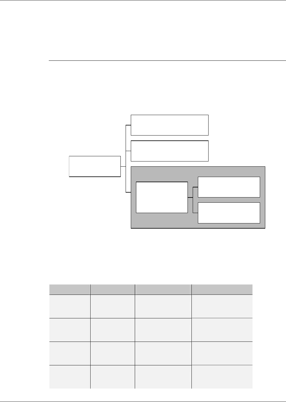
1.1 Related Documents
The picture below shows the relation between the different Serial Port Adapter documents.
Bluetooth Enabler Development Kit
Ser i al Po r t A dap t er
User Manual
Ser ial Po r t Ad ap t er
AT Commands
OEM Serial Port Adapter
Electrical & Mechanical Datasheet
ECI Dr i ver w i t h
connectBlue
Extensions
User Manual
ECI Specification
ECI Specification with
connectBlue Extensions
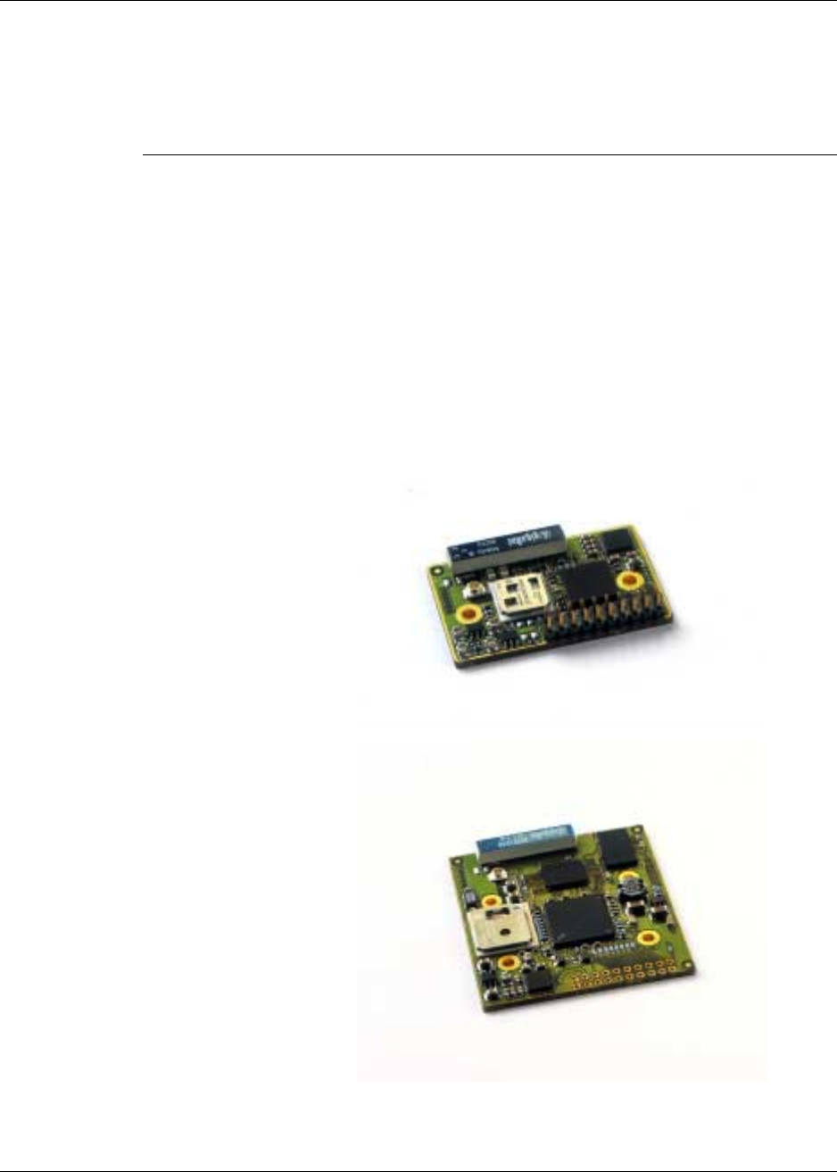
1.2 Product Variants
This Electrical and Mechanical datasheet contains information about the second generation
of OEM Serial Port Adapter. The design consists of two different modules cB-0701-01 (Class
2 / 1 mW / 0 dBm) and cB-0702-01 (Class 1 / 100 mW / 20 dBm).
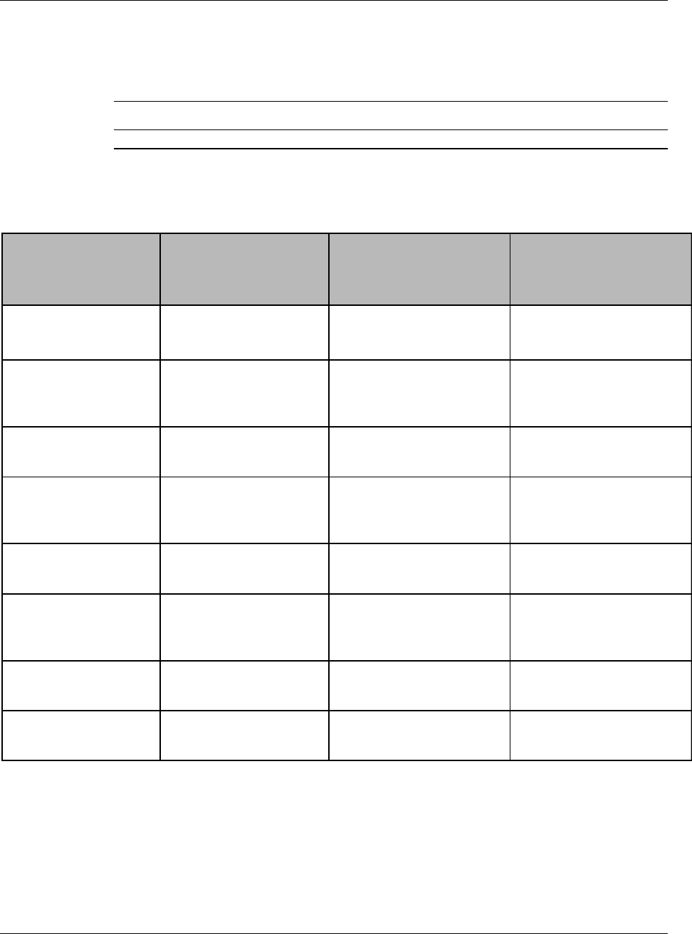
Product Name OEM Module ID Type Description
OEMSPA13i cB-0701-01 Class 2 / 0 dBm OEM Serial Port
Adapter 13i with
internal antenna
OEMSPA13x cB-0701-01 Class 2 / 0 dBm OEM Serial Port
Adapter 13x with
external antenna
OEMSPA33i cB-0702-01 Class 1 / 20 dBm OEM Serial Port
Adapter 33i with
internal antenna
OEMSPA33x cB-0702-01 Class 1 / 20 dBm OEM Serial Port
Adapter 33x with
external antenna

6
cB-0701-01
cB-0701-01 is a small size Bluetooth module based on the Infineon (former Ericsson) PBM
990 80 baseband controller and the PBA 313 05 0dBm radio.
The PBM 990 80 has 64 Kbytes on chip SRAM and 512 Kbytes FLASH stacked in the same
package.
cB-0702-01
cB-0702-01 is a long-range versatile Bluetooth module based on the Infineon (former
Ericsson) PBM 990 90 baseband controller and the PBA 313 02 20 dBm radio.
The PBM 990 90 has 64 Kbytes on chip SRAM, the FLASH is located in a separate
package.
cB-0702-01 also contains external SRAM.
7
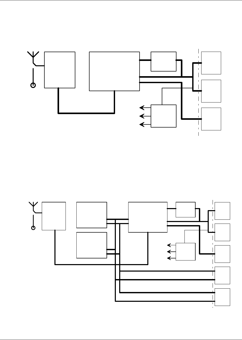
1.3 Block Diagram cB-0701-01
1.4 Block Diagram cB-0702-01
ADR[1..22]
DATA[0..15]
ADR[0..19]
DATA[0..7]
Base Band Controller
PBM990 90 (BLINK)
FLASH
1 - 8Mbyte
SRAM
128k - 1Mbyte
EBC radio interface
RS-232
Transceiver
ADM3315
Bluetooth-
Radio
PBA
313 02
(MIRIAN)
Power
supply
Vin=3.3-6V
Module Interface
ADR[0..23]
DATA[0..15]
Internal antenna
External
Antenna connector
J1
J2
J4
J5
J3
J6
Base Band Controller
PBM990 80 (FLINK)
EBC radio interface
RS-232
Transceiver
ADM3315
Bluetooth-
Radio
PBA
313 05
(RAN)
Power
supply
Vin=3.3-6V
Module InterfaceInternal antenna
External
Antenna connector
J1
J2
J3
J6
Vin=3-6V
8
Chapter 2
Electrical Interface and Connectors
This section describes the signals available on the module interface connectors. There are
two ways to connect to the OEM Serial Port Adapter, one is via the J1 connector, a 20-pin
2mm pitch pin header, and the other is via the board-to-board (one piece part) connector, J2
through J5.
NOTE! J4 and J5 are only available on cB-0702-01
The J2 to J5 connectors on the OEM Serial Port Adapter exist on the module only as a
mating PCB-layout pattern.
NOTE! Connectors J3 to J5 are for future use only and will not be covered in details
by this document.
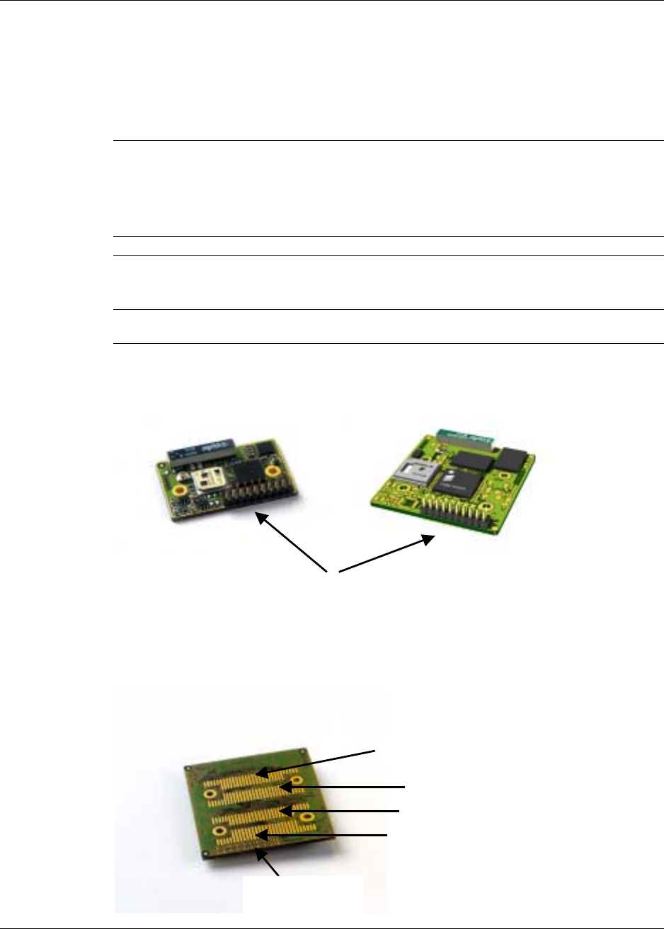
cB-0701-01 with J1 cB-0702-01 with J1
J1 connector - 20-pin 2mm pitch pin header
CB-0702-01 with J2 to J5 (mating PCB-layout pattern)
J1 connector
(back side)
J2 connector
J3 connector
J4 connector
J5 connector
9
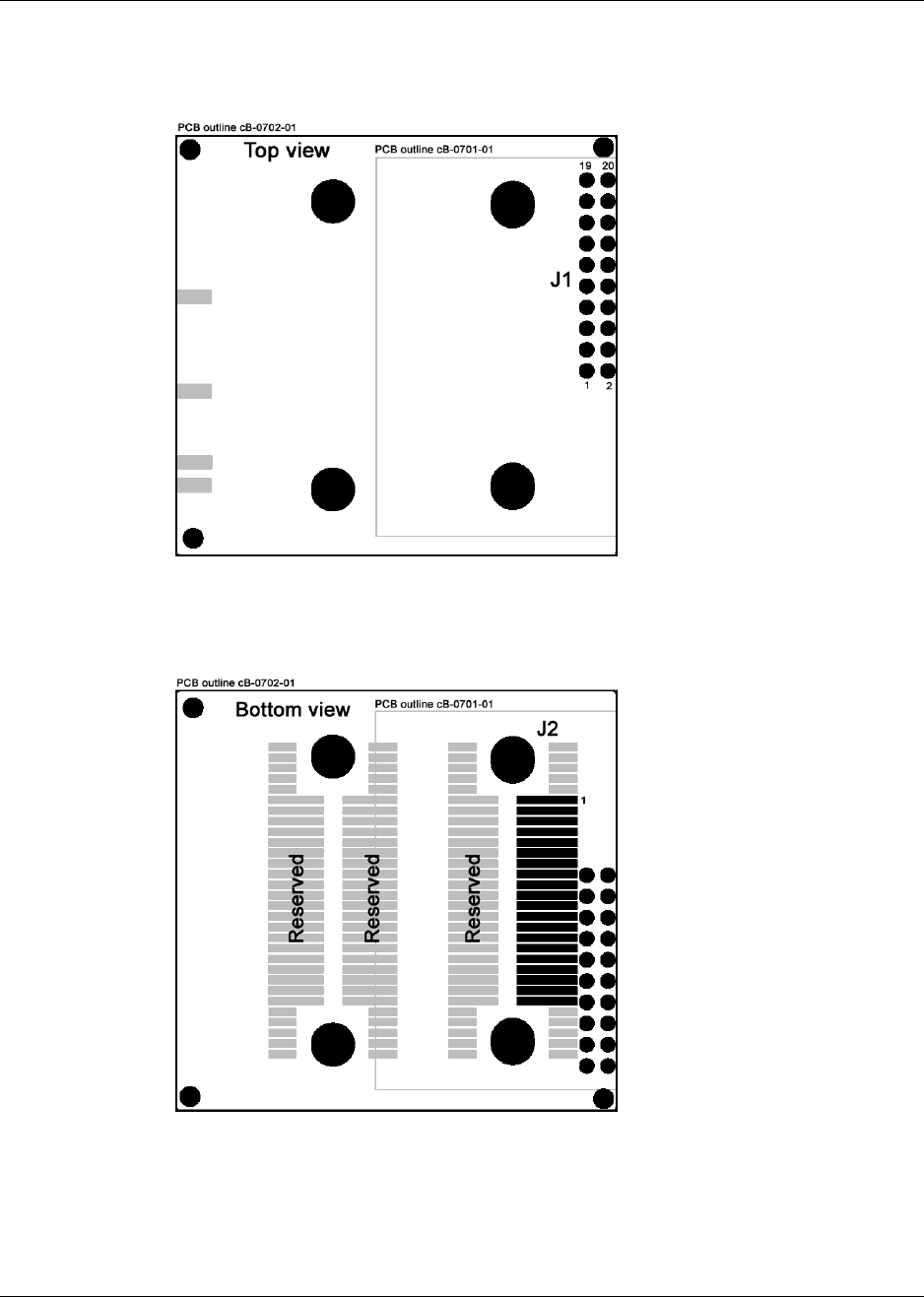
J1 connector
The figure above shows the pin numbering of the J1 connector.
J2 connector
The figure shows the bottom view of the two PCBs and the pinning of the J2 connector.
10
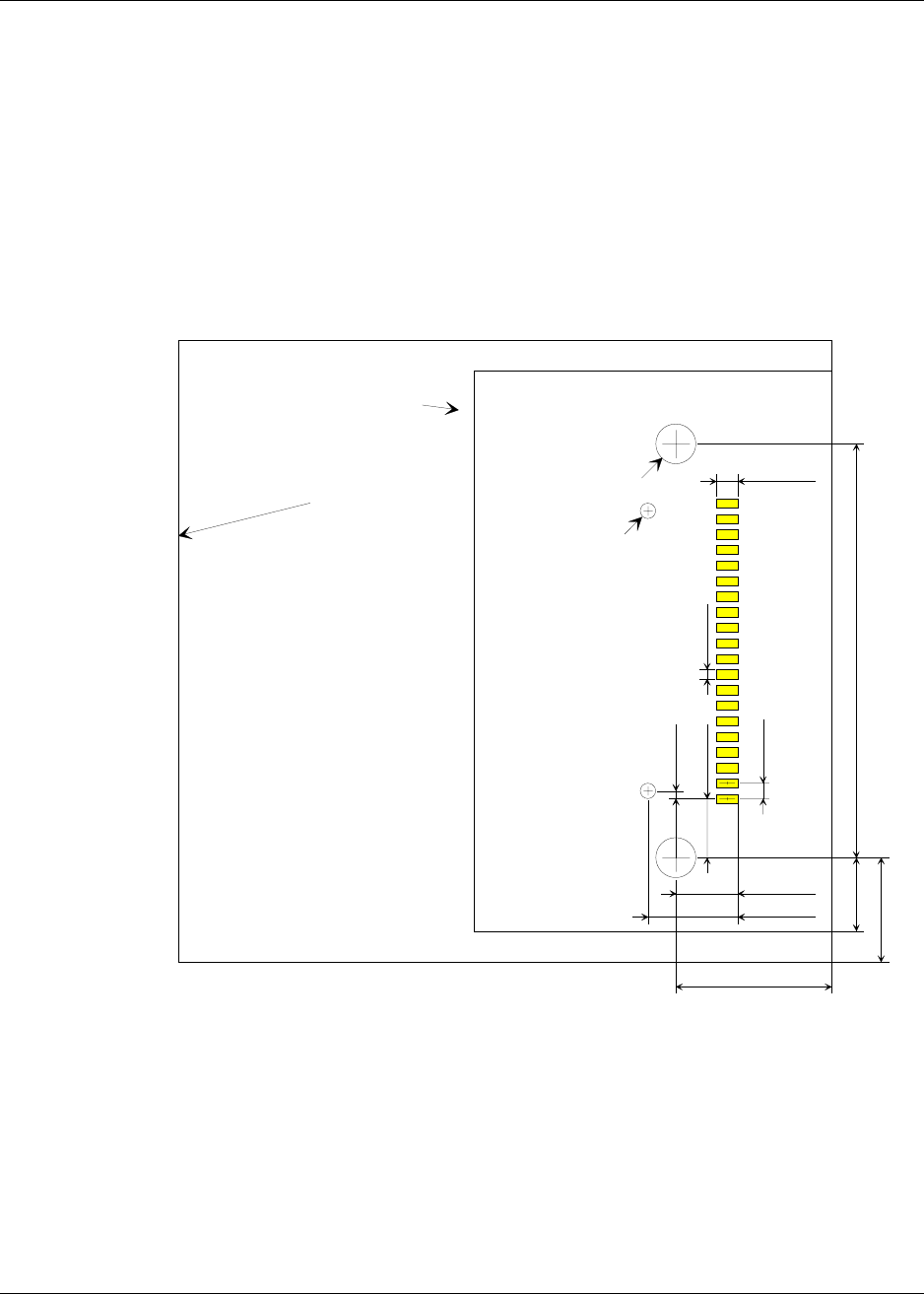
J2 motherboard connectors
A single-row connector may be used. A connector of the following type is recommended:
Samtec: SEI-120-02-GF-S-M-AB
The height of this connector is 1.65 mm.
2 x Ø1.0 mm
Mother board footprint for single row
module interface J2
Samtec type:
SEI-120-02-GF-S-M-AB
1.0mm
0.5mm
4.0mm
5.84mm
3.81mm
2 x Ø2.5 mm
0.56mm
PCB-outline
cB-0701-01
PCB-outline
cB-0702-01
10.0mm
4.69mm
6.69mm26.62mm
1.35mm
1
A double-row connector may be used although all the pins needed to use are available on
the J2 connector only. The connector is connected to the pins of the J2 and J3 connector. A
double-row connector of the following type is recommended:
Samtec: FSI-120-03-G-D-M-AB
The height of this connector is 3.00 mm.
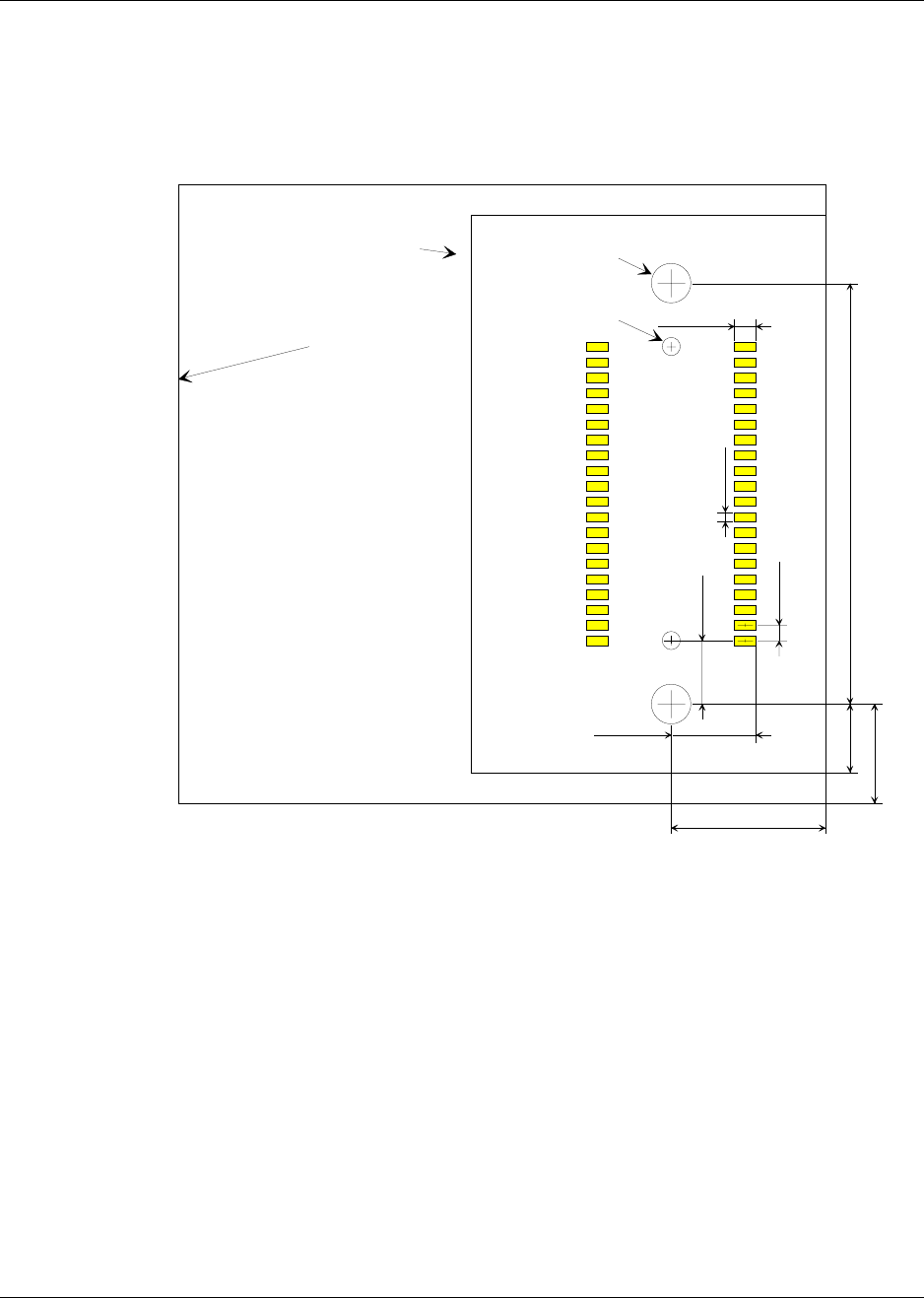
11
2 x Ø1.2 mm
Mother board footprint for double row
module interface J2 & J3
Samtec type:
FSI-120-03-G-D-M-AB
1.0mm
5.28mm
4.12mm
2 x Ø2.5 mm
0.56mm
PCB-outline
cB-0701-01
PCB-outline
cB-0702-01
10.0mm
4.38mm
6.38mm27.24mm
1.14mm
11
J2J3
Other connector alternatives maybe used. Use the diagrams above for design help.
12
2.1 CMOS Logic Levels
The boards cB-0701-01 and cB-0702-01 has some signals that are defined as logic level
CMOS signals. The boards are designed to be fully interchangeable between each other.
This is possible if the host product has made space for the cB-0702-01 board. This makes it
possible to choose freely between a class 1 or class 2 device without any change of the host
product.
The following voltage conditions are valid.
Signal Voltage level Remark
Vin Low min - 0.3 V
Vin Low max 0.8 V 0.95 V if only cB-0702-01 is used
Vin High min 2.25 V 2.05 V if only cB-0701-01 is used
Vin High max 3.2 V 3.5 V if only cB-0702-01 is used
Vout Low max 0.1 V
Vout High min 2.8 V
13
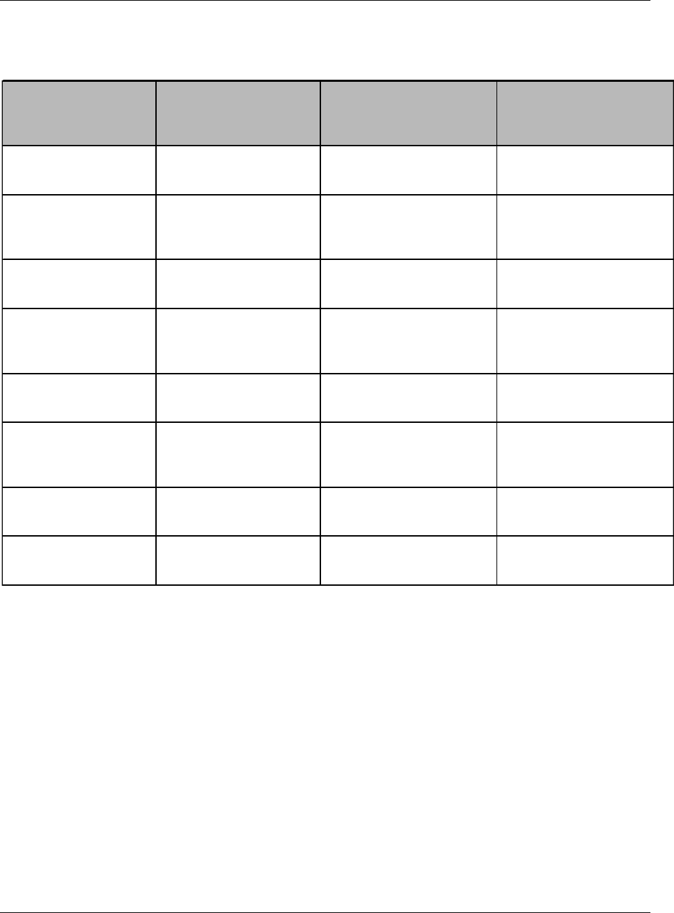
2.2 Signals in J1 and J2 Connector
Maximum load on all In/Out is 3mA.
J1 &
J2
Pin nr.
Pin Name Signal Name Signal
Level Type Description
1 VSS Ground Ground
2 VSS Ground Ground
3 VCC_5V Power 3.3V – 6V If only cB-0701-01 is used the
range 3.0V – 6.0V is allowed
4 VCC_5V Power 3.3V – 6V If only cB-0701-01 is used the
range 3.0V – 6.0V is allowed
5 RS232-CTS Clear To Send RS232 Input
6 RS232-TxD Transmit Data RS232 Output
7 RS232-RTS Request To Send RS232 Output
8 RS232-RxD Receive Data RS232 Input
9 RS232-DTR Data Terminal Ready RS232 Output
10 RS232-DSR Data Set Ready RS232 Input Also used to control the power
saving mode “stop mode”.
See chapter 2.4 for more
information.
11 RED/Mode Red LED output and
Serial interface mode
select input
CMOS In/Out The level on this pin during
power up selects RS232 (High)
or logic (Low) level UART-
communication.
The Mode pin is only valid at
startup and cannot be changed
during operation.
The Mode pin is internally
pulled up i.e. RS232 mode is
the default setting.
Recommended value of the
pull-down resistor is 10 kohm.
See section 2.5 for a design
example.
12 Switch-0 Function switch CMOS In Used for the “Connect on
external signal” function, see
the Serial Port Adapter user
manual for more information on
the Function switch.
See section 2.5 for a design
example.
14
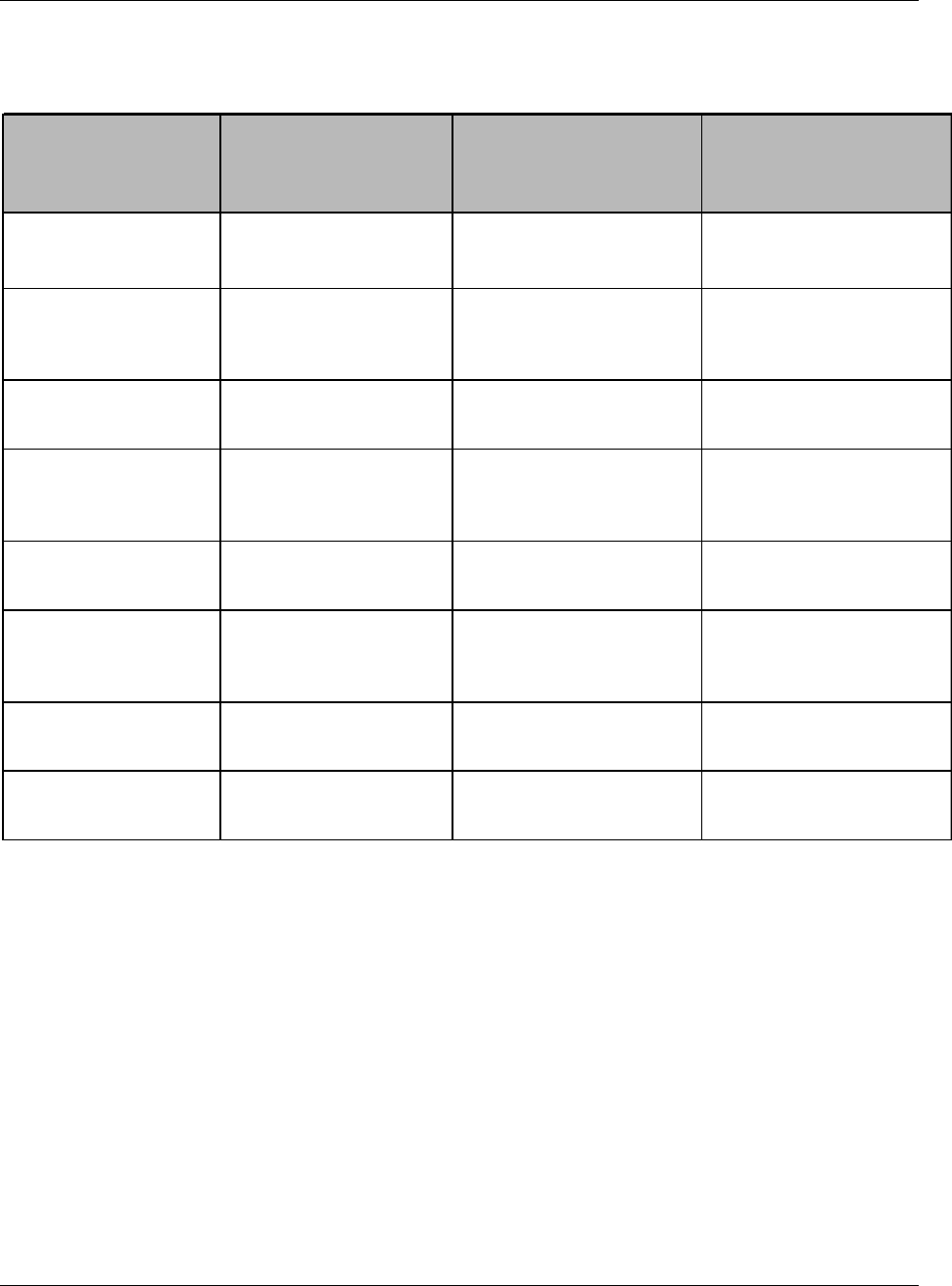
J1 &
J2
Pin nr.
Pin Name Signal Name Signal
Level Type Description
13 GREEN/Switch-1 Green LED output
and Restore switch CMOS In/Out If the level on this pin is set to
Low the units goes back to
default serial settings.
The “Restore Default” input is
only active at unit power up.
See the Serial Port Adapter
user manual for more
information on the Restore
switch.
See section 2.5 for a design
example.
14 BLUE Blue LED output CMOS Output See section 2.5 for a design
example.
15 UART1-CTS Clear To Send CMOS Input See Note 1 below.
16 UART1-TxD Transmit Data CMOS Output
17 UART1-RTS Request To Send CMOS Output
18 UART1-RxD Receive Data CMOS Input See Note 1 below.
19 UART1-DTR Data Terminal Ready CMOS Output
20 UART1-DSR Data Set Ready CMOS Input Also used to control “stop down
mode”. See chapter 2.4 for
more information.
NOTE1! It is recommended to connect a “pull-up” resistor with the value 82 kohm to
2.8 VDC if UART1-CTS and/or UART-RxD are unconnected or may be left in an
undefined state.
2.3 Signals in J3 – J5 Connector
These connectors are for future use and not covered by this document..
2.4 Power Control
The DSR signal on the UART and the RS232 interfaces may be used to control “stop mode”.
“Stop mode” is the most efficient power saving mode.
For more information about “stop mode”, see the Serial Port Adapter User Manual.
15
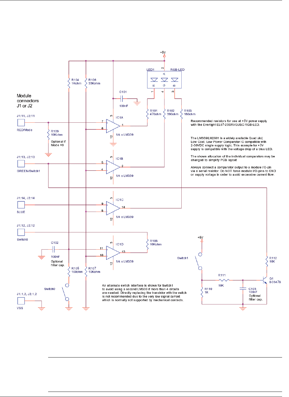
2.5 Interfacing Examples
Example 1 – connection of input/output pins
Example 2 – Input/output pins connected to a Host CPU
It is recommended to use a serial resistance with a 10 kohm value between the host CPU
and the connectBlue module for all input and output pins.
NOTE! The RED/Mode pin is a combined output/input pin. The Mode input is only
active at power up of the unit.
NOTE! The GREEN/Switch 1 pin is a combined output/input pin. The Switch 1 input is
only active at power up of the unit.
16
Chapter 3
Temperature Information
In the tables below you find information about the different temperature conditions.
CB-0701-01
Storage temperature -40 - +85 °C
Recommended operating temperature -20 - +75 °C
Maximum operating temperature -30 - +75 °C
CB-0702-01
Storage temperature -40 - +85 °C
Recommended operating temperature -30 - +55 °C
Maximum operating temperature -30 - +75 °C
17
Chapter 4
Bluetooth Information
In the tables below you find information about product Bluetooth properties.
CB-0701-01
Bluetooth Radio Infineon/Ericsson PBD 313 05 (RAN)
Bluetooth Base Band Controller Infineon/Ericsson PBM 990 80 (FLINK)
RF Output power Class 2, min –2dBm type 1.5dBm
max +4dBm
Receive sensitive level -80dBm (0.1% BER)
Receive input level (Max) Max +14 dBm
Output frequency 2.4 –2.5 GHz, ISM band.
Point to multi-point operation Yes
Bluetooth stack Embedded Host Stack
Bluetooth qualification 1.1
CB-0702-01
Bluetooth Radio Infineon/Ericsson PBD 313 02 (MIRIAN)
Bluetooth Base Band Controller Infineon/Ericsson PBM 990 90 (BLINK)
RF Output power Class 1, min –28dBm, max +16.9dBm
Receive sensitive level -80dBm (0.1% BER)
Receive input level (Max) Max +15 dBm
Output frequency 2.4 –2.5 GHz, ISM band.
Point to multi-point operation Yes
Bluetooth stack Embedded Host Stack
Bluetooth qualification 1.1
18
Chapter 5
Power Consumption
NOTE! The power consumption depends on the UART speed chosen.
CB-0701-01 (up to 57,6 kBits/s UART baud rate)
Input power is 5 VDC. No external LEDs are connected. UART baud rates up to 57,6 kBits/s.
Input voltage : 5V
Baudrate <= 57,6 no load on output signals
RS232 circuit enabled logic level UART signals
loaded (Tx, Rx) RS232
circuit disabled
RS232 signals loaded (Tx,
RTS, DTR, @3000
ohm/signal) RS232 circuit
enabled
not connected, not
connectable, not
discoverable
typical mean (mA) : 26.2
typical max (mA) : 26.8 typical mean (mA) : 25.2
typical max (mA) : 25.2 typical mean (mA) : 50.1
typical max (mA) : 50.2
not connected, not
connectable, not
discoverable, stop mode
enabled
typical mean (mA) : 0.7
typical max (mA) : 1.4
typical mean (mA) : 0.6
typical max (mA) : 0.7
typical mean (mA) : 24.5
typical max (mA) : 24.6
not connected,
connectable, not
discoverable
typical mean (mA) : 27.4
typical max (mA) : 88.5
typical mean (mA) : 27.2
typical max (mA) : 86.6
typical mean (mA) : 50.7
typical max (mA) : 106.9
not connected,
connectable, not
discoverable, stop mode
enabled
typical mean (mA) : 1.1
typical max (mA) : 87.1 typical mean (mA) : 1.1
typical max (mA) : 86.2 typical mean (mA) : 25.3
typical max (mA) : 107.9
not connected,
connectable,
discoverable
typical mean (mA) : 27.9
typical max (mA) : 88.7 typical mean (mA) : 27.8
typical max (mA) : 86.6 typical mean (mA) : 51.1
typical max (mA) : 107.1
not connected,
connectable,
discoverable, stop mode
enabled
typical mean (mA) : 2.3
typical max (mA) : 87.2
typical mean (mA) : 2.3
typical max (mA) : 86.8
typical mean (mA) : 26.0
typical max (mA) : 107.8
connected idle,
connectable, not
discoverable
typical mean (mA) : 35.8
typical max (mA) : 104.7
typical mean (mA) : 35.6
typical max (mA) : 107.9
typical mean (mA) : 58.6
typical max (mA) : 126.5
connected send data,
connectable, not
discoverable
N/A typical mean (mA) : 52
typical max (mA) : 106.4
typical mean (mA) : 65 typical
max (mA) : 126.5
19
CB-0701-01 (higher than 57,6 kBits/s UART baud rate)
Input power is 5 VDC. No external LEDs are connected. UART baud rates higher than 57,6
kBits/s.
Input voltage : 5V
Baudrate > 57,6 no load on output signals
RS232 circuit enabled logic level UART signals
loaded (Tx, Rx) RS232
circuit disabled
RS232 signals loaded
(Tx,RTS, DTR @3000
ohm/signal) RS232 circuit
enabled
not connected, not
connectable, not
discoverable
typical mean (mA) : 60.8
typical max (mA) : 61.4
typical mean (mA) : 61.0
typical max (mA) : 61.0
typical mean (mA) : 83.6
typical max (mA) : 83.6
not connected, not
connectable, not
discoverable, stop mode
enabled
typical mean (mA) : 0.8
typical max (mA) : 1.6
typical mean (mA) : 0.6
typical max (mA) : 1.3
typical mean (mA) : 24.5
typical max (mA) : 24.6
not connected,
connectable, not
discoverable
typical mean (mA) : 63.9
typical max (mA) : 120.5
typical mean (mA) : 64.2
typical max (mA) : 123.5
typical mean (mA) : 86.7
typical max (mA) : 142.6
not connected,
connectable, not
discoverable, stop mode
enabled
typical mean (mA) :1.6
typical max (mA) : 88.7 typical mean (mA) : 1.5
typical max (mA) : 87.1 typical mean (mA) : 25.3
typical max (mA) : 107.9
not connected,
connectable,
discoverable
typical mean (mA) : 64.3
typical max (mA) : 121.0 typical mean (mA) : 64.7
typical max (mA) : 123.5 typical mean (mA) : 87.1
typical max (mA) : 154.6
not connected,
connectable,
discoverable, stop mode
enabled
typical mean (mA) : 2.4
typical max (mA) : 88.4
typical mean (mA) : 2.6
typical max (mA) : 92.0
typical mean (mA) : 26.0
typical max (mA) : 107.4
connected idle,
connectable, not
discoverable
typical mean (mA) : 73.3
typical max (mA) : 141.0
typical mean (mA) : 73.8
typical max (mA) : 155.0
typical mean (mA) : 96.0
typical max (mA) : 172.1
connected send data,
connectable, not
discoverable
N/A typical mean (mA) : 87.6
typical max (mA) : 156.3
typical mean (mA) : 100
typical max (mA) : 173
20
CB-0702-01 (up to 57,6 kBits/s UART baud rate)
Input power is 5 V. No external LEDs are connected. UART baud rates up to 57,6 kBits/s.
Input voltage : 5V
Baudrate <= 57,6 no load on output signals
RS232 circuit enabled logical level UART signals
loaded (Tx, Rx) RS232
circuit disabled
RS232 signals loaded (Tx,
RTS, DTR, @3000
ohm/signal) RS232 circuit
enabled
not connected, not
connectable, not
discoverable
typical mean (mA) : 17.6
typical max (mA) : 20.8 typical mean (mA) : 17.5
typical max (mA) : 19.1 typical mean (mA) : 32.6
typical max (mA) : 36.6
not connected, not
connectable, not
discoverable, stop mode
enabled
typical mean (mA) : 0.5
typical max (mA) : 7.4
typical mean (mA) : 0.5
typical max (mA) : 6.2
typical mean (mA) : 16.3
typical max (mA) : 20.2
not connected,
connectable, not
discoverable
typical mean (mA) : 18.7
typical max (mA) : 65.6
typical mean (mA) : 19.0
typical max (mA) : 65.0
typical mean (mA) : 33.6
typical max (mA) : 81.3
not connected,
connectable, not
discoverable, stop mode
enabled
typical mean (mA) : 0.7
typical max (mA) : 22.3 typical mean (mA) : 0.6
typical max (mA) : 22 typical mean (mA) : 16.6
typical max (mA) : 81.8
not connected,
connectable,
discoverable
typical mean (mA) : 18.7
typical max (mA) : 65.6 typical mean (mA) : 18.9
typical max (mA) : 64.8 typical mean (mA) : 33.6
typical max (mA) : 81.1
not connected,
connectable,
discoverable, stop mode
enabled
typical mean (mA) : 1.0
typical max (mA) : 22.4
typical mean (mA) : 0.5
typical max (mA) : 21.7
typical mean (mA) : 16.9
typical max (mA) : 82.2
connected idle,
connectable, not
discoverable
typical mean (mA) : 27.3
typical max (mA) : 172.9
typical mean (mA) : 26.9
typical max (mA) : 172.1
typical mean (mA) : 43.0
typical max (mA) : 193.5
connected send data,
connectable, not
discoverable
N/A typical mean (mA) : 35
typical max (mA) : 172.6
typical mean (mA) : 50.0
typical max (mA) : 194

21
CB-0702-01 (higher than 57,6 kBits/s UART baud rate)
Input power is 5 V. No external LEDs are connected. UART baud rates higher than 57,6
kBits/s.
Input voltage : 5V
Baudrate > 57,6 no load on output signals
RS232 circuit enabled logical level UART signals
loaded (Tx, Rx) RS232
circuit disabled
RS232 signals loaded
(Tx,RTS, DTR @3000
ohm/signal) RS232 circuit
enabled
not connected, not
connectable, not
discoverable
typical mean (mA) : 39.7
typical max (mA) : 40.1
typical mean (mA) : 39.6
typical max (mA) : 39.7
typical mean (mA) : 53.6
typical max (mA) : 53.6
not connected, not
connectable, not
discoverable, stop mode
enabled
typical mean (mA) : 0.6
typical max (mA) : 7.3
typical mean (mA) : 0.4
typical max (mA) : 5.7
typical mean (mA) : 16.3
typical max (mA) : 18.9
not connected,
connectable, not
discoverable
typical mean (mA) : 41.7
typical max (mA) : 89.3
typical mean (mA) : 41.2
typical max (mA) : 87.9
typical mean (mA) : 55.6
typical max (mA) : 105.3
not connected,
connectable, not
discoverable, stop mode
enabled
typical mean (mA) : 0.9
typical max (mA) : 65.0 typical mean (mA) : 1.1
typical max (mA) : 66.1 typical mean (mA) : 16.5
typical max (mA) : 82.3
not connected,
connectable,
discoverable
typical mean (mA) : 42.1
typical max (mA) : 88.1 typical mean (mA) : 42.0
typical max (mA) : 87.6 typical mean (mA) : 56.0
typical max (mA) : 105.7
not connected,
connectable,
discoverable, stop mode
enabled
typical mean (mA) : 1.3
typical max (mA) : 66.0
typical mean (mA) : 1.1
typical max (mA) : 66.2
typical mean (mA) : 17.3
typical max (mA) : 82.4
connected idle,
connectable, not
discoverable
typical mean (mA) : 49.6
typical max (mA) : 212.3
typical mean (mA) : 49.2
typical max (mA) : 211.5
typical mean (mA) : 65.4
typical max (mA) : 234.6
connected send data,
connectable, not
discoverable
N/A typical mean (mA) : 78
typical max (mA) : 214.3
typical mean (mA) : 94.0
typical max (mA) : 237.5
22
Chapter 6
Antennas
There are 2 different antenna options available:
• An internal surface mounted (SMD) antenna.
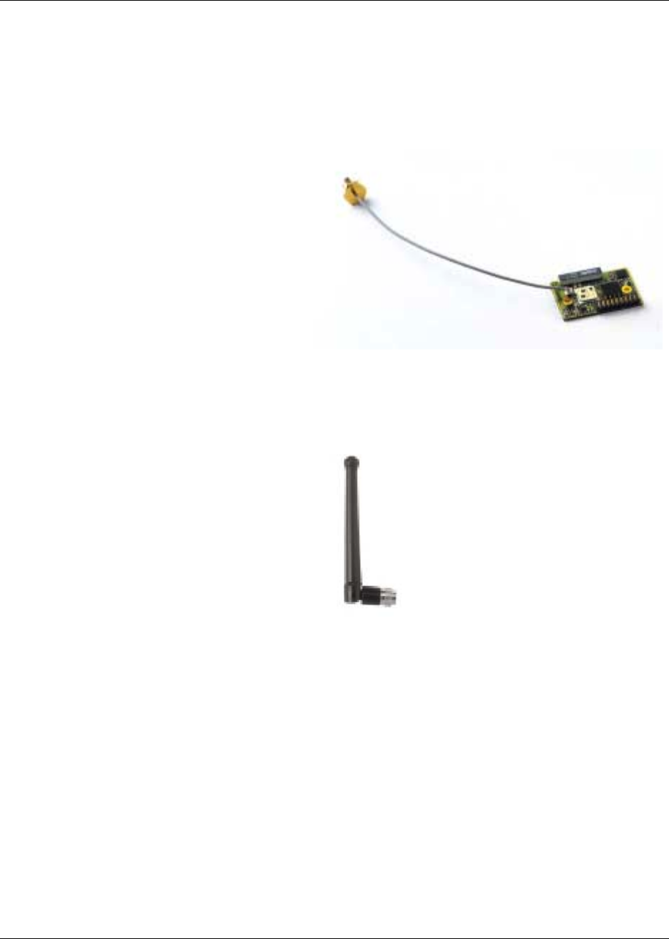
• An “antenna on a cable” maybe connected to a U.FL connector. Three different
“antennas on a cable” are available.
See chapter about Mounting for more info about antenna placement.
This chapter gives only an overview of the qualities of the different antenna options. More
detailed information is available in the antenna data sheets.
6.1 Surface Mounted Antenna (internal)
The unit cannot be mounted in a metal-shielded enclosure with this antenna.
cB-0701-01
Polarization Linear
cB-0702-01
Polarization Linear
23
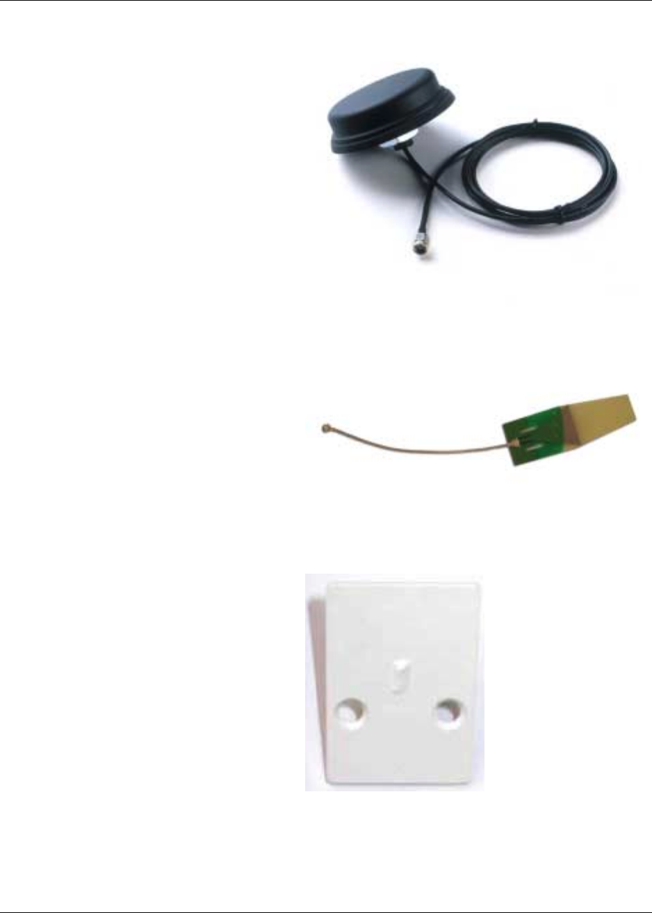
6.2 Antennas on a Cable (external antennas)
The external antennas are connected to the board through a U.FL connector. Some of the
antennas are connected directly to the U.FL connector of the board and some is connected
using a SMA connected through a short U.FL to SMA adapter cable.
Antenna Accessories
Part number cB-ACC-18
Name U.FL to SMA
adapter
cable
Connector U.FL and
SMA
Comment The SMA connector maybe mounted in a panel. The length is of the cable
is 12 cm.
Antennas
Part number cB-ACC-16
Name WCR-2400-
SMA
Type ½ wave
dipole
Polarization Vertical
Size 10 cm
Connector SMA
Comment To be mounted on the UF.L to SMA adapter cable.
24
Part number cB-ACC-17
Name Puck
Antenna
Type
Polarization
Size 70 mm in
diameter.
Connector SMA
Comment To be mounted on the UF.L to SMA adapter cable. The antenna is
mounted with a 16 mm hole through a cabinet wall or ceiling.
Part number cB-ACC-19
Name CAP24235
(Microblue)
Type Microstrip
Polarization Linear
Size 21x60 mm.
20 cm cable.
Connector U.FL
Comment Connected directly to the U.FL connector on OEM board.
Part number cB-ACC-20
Name CAF94146
Microsphere
Type Microstrip
Polarization Linear
Size 46x30 mm.
2.5 mm high.
20 cm cable.
Connector U.FL
Comment Connected directly to the U.FL connector on OEM board. Delivered with a
mounting kit.
25
Chapter 7
Additional Mounting Instructions
7.1 Antenna Issues
The unit cannot be mounted arbitrary, because of the radio communication. The unit with an
internal surface mounted antenna cannot be mounted in a metal enclosure. If a metal
enclosure is required, one of the external antenna options has to be used.
Use one of the external antenna options if you are using a metallic enclosure or if there are
other reasons why the internal antenna cannot be used. See section 6.2 for more information
on the antenna options available.
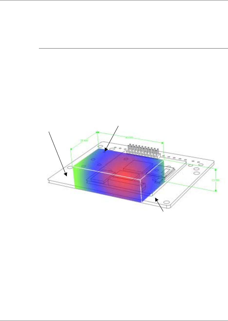
7.2 Traces and Component Keep out Area
The 20-pin 2 mm pitch pin connector (J1) sticks out 1.2 mm below the bottom side of the
Serial Port boards.
It is recommended to keep traces and components out of this area on the motherboard or
keep a safe distance between the motherboard and the Serial Port Adapter board (> 1.6
mm).
See chapter 8.1 for detailed measurements and positions for the J1 connector.
7.3 Using the 20-pin 2 mm Pitch Pin Connector
If you mount the boards on a motherboard using the mounting holes, distances must be
used that is higher than 1.6 mm, this due to the pins of the J1 connector (see chapter 7.2).
Chapter 2 contains more information about the connector and the electrical interface.
A recommended space around the SMD antenna
must be free from wires, circuits or other conductive
components of the user application.
Illustration of a
user
application
OEM Bluetooth module

26
7.4 Using Board-to-Board Connectors
Reserved Area
Make place for the 20-pin 2 mm pitch pin connector as indicated in chapter 7.2. This allows
you to use a standard connectBlue OEM Serial Port Adapter even tough you are not using
this connector. Contact connectBlue if there is a requirement to used this reserved area for
components.
Using the SEI-120-02-GF-S-M-AB Connector from Samtec
This connector has a profile height of 1.65 mm and this has to be considered if components
are to be mounted on the motherboard under the Serial Port Adapter board.
The connector has 2 mm threaded inserts that fit with the mounting holes in the board. You
may screw the Serial Port board directly into this inserts. If you want to have a tighter and
more secure mounting you may use longer screws and secure it using a nut on the backside
of the motherboard.
Chapter 2 contains more information about the connector, necessary measurements on the
motherboard and the electrical interface.
Using the FSI-120-03-G-D-M-AB connector from Samtec
This connector has a height of 3.0 mm and this has to be considered if components are to be
mounted on the motherboard under the Serial Port Adapter board.
The connector has 2 mm threaded inserts that fit with the mounting holes in the board. You
may screw the Serial Port board directly into this inserts. If you want to have a tighter and
more secure mounting you may use longer screws and secure it using a nut on the backside
of the motherboard.
Chapter 2 contains more information about the connectors, mounting measurements and the
electrical interface.
27
Chapter 8
Mechanics
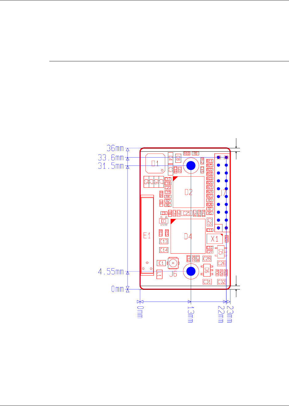
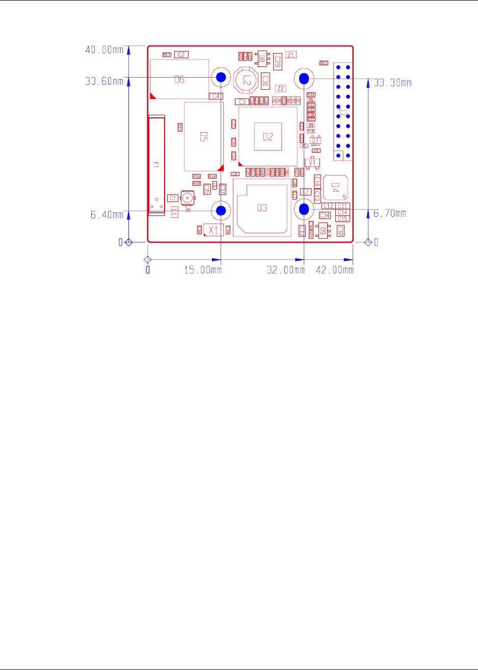
8.1 Board Outlines
The smaller board cB-0701-01 is 36x23x1.45 mm. The larger board is 40x42x1.45 mm. The
height of the module is maximum 5 mm. No components are mounted on the secondary side
of the module.
0.9 mm
0.9 mm
PCB-outline cB-0701-01
28
PCB-outline cB-0702-01
29
Chapter 9
Regulatory Information
9.1 Declaration of Conformity
We, connectBlue AB, of
Stora Varvsgatan 11 N:1
SE-211 19 Malmö, Sweden
declare under our sole responsibility that our products:
OEM Serial Port Adapter 13i, cB-0032-01, OEM Serial Port Adapter 13x, cB-0033-01
OEM Serial Port Adapter 33i, cB-0034-01, OEM Serial Port Adapter 33x, cB-0035-01
Serial Port Adapter 12i, cB-0036-01, Serial Port Adapter 32i, cB-0037-01
Serial Port Adapter 33i, cB-0041-01, Serial Port Adapter 33c, cB-0038-01
Rugged Serial Port Adapter 32s, cB-0039-01, OEM Module Adapter 2, cB-0040-01
to which this declaration relates, conforms to the following product specifications:
R&TTE Directive 1999/5/EC
EN 300 328-2 V1.1.1 (2000-07)
EMC Directive: 89/336/EEC
EN 301 489-1 V1.3.1 (2001-09)
EN 301 489-17 V1.1.1 (2000-09)
EN 61000-6-2 (1999)
Low Voltage Directive: 73/23/EEC
EN 61131-2
Medical Electrical Equipment
IEC 60601-1-2
A notification must be made to each of the national authorities responsible for radio spectrum
management of the intention to place radio equipment that uses frequency bands whose use
is not harmonized throughout the EU, on its national market.
More information at: http://europa.eu.int/comm/enterprise/rtte/gener.htm
30
9.2 FCC Compliance
FCC Statement for cB-0701-01
This device complies with Part 15 of the FCC Rules. Operation is subject to the following two
conditions: (1) this device may not cause harmful interference, and (2) this device must
accept any interference received, including interference that may cause undesired operation.
NOTE: This equipment has been tested and found to comply with the limits for a Class B digital
device, pursuant to Part 15 of the FCC Rules. These limits are designed to provide
reasonable protection against harmful interference in a residential installation. This
equipment generates, uses and can radiate radio frequency energy and, if not installed and
used in accordance with the instructions, may cause harmful interference to radio
communications. However, there is no guarantee that interference will not occur in a
particular installation. If this equipment does cause harmful interference to radio or television
reception, which can be determined by turning the equipment off and on, the user is
encouraged to try to correct the interference by one or more of the following measures:
• Reorient or relocate the receiving antenna
• Increase the separation between the equipment and receiver
• Connect the equipment into an outlet on a circuit different from that to which the receiver
is connected
• Consult the dealer or an experienced radio/TV technician for help
Labeling Requirements for End Product
For an end product using the OEM Serial Port Adapter or the OEM Bluetooth Enabler there
must be a label containing, at least, the following information:
The label must be affixed on an exterior surface of the end product such that it will be visible
upon inspection in compliance with the modular approval guidelines developed by the FCC.
In addition, the user manual for the end product must contain the following information:
“This device complies with Part 15 of the FCC Rules. Operation is subject to the following
two conditions: (1) this device may not cause harmful interference, and (2) this device must
accept any interference received, including interference that may cause undesired
operation.”
Antenna
When using the module equipped with the external antennas as described previously the
antenna is fixed and cannot be removed or replaced by the end user.
Caution
Any changes or modifications NOT explicitly APPROVED by connectBlue AB could cause
the module to cease to comply with FCC rules part 15, and thus void the user’s authority to
operate the equipment.
This device contains
FCC ID: PVH070101
31
FCC Statement for cB-0702-01
This device complies with Part 15 of the FCC Rules. Operation is subject to the following two
conditions: (1) this device may not cause harmful interference, and (2) this device must
accept any interference received, including interference that may cause undesired operation.
NOTE: This equipment has been tested and found to comply with the limits for a Class B digital
device, pursuant to Part 15 of the FCC Rules. These limits are designed to provide
reasonable protection against harmful interference in a residential installation. This
equipment generates, uses and can radiate radio frequency energy and, if not installed and
used in accordance with the instructions, may cause harmful interference to radio
communications. However, there is no guarantee that interference will not occur in a
particular installation. If this equipment does cause harmful interference to radio or television
reception, which can be determined by turning the equipment off and on, the user is
encouraged to try to correct the interference by one or more of the following measures:
• Reorient or relocate the receiving antenna
• Increase the separation between the equipment and receiver
• Connect the equipment into an outlet on a circuit different from that to which the receiver
is connected
• Consult the dealer or an experienced radio/TV technician for help
Labeling Requirements for End Product
For an end product using the OEM Serial Port Adapter or the OEM Bluetooth Enabler there
must be a label containing, at least, the following information:
The label must be affixed on an exterior surface of the end product such that it will be visible
upon inspection in compliance with the modular approval guidelines developed by the FCC.
In addition, the user manual for the end product must contain the following information:
“This device complies with Part 15 of the FCC Rules. Operation is subject to the following
two conditions: (1) this device may not cause harmful interference, and (2) this device must
accept any interference received, including interference that may cause undesired
operation.”
RF-exposure statement
This portable modular transmitter MUST have a separation distance of at least 2.5cm
between the antenna and the body of the user or nearby persons, excluding hands, wrists,
feet, and ankles.
If the radio module is installed in a laptop display, transmission MUST be prevented if the lid
is closed to ensure that the minimum distance of 2.5cm between the user and the
transmitting antenna is maintained.
Any notification to the end user of installation or removal instructions about the integrated
radio module is NOT allowed.
This device contains
FCC ID: PVH070201

32
Antenna
When using the module equipped with the external antennas as described previously the
antenna MUST be fixed, not to be able to be removed or replaced by the end user.
On modules equipped with SMA-connector, the connector-antenna thread MUST be locked
with LOCTITE ® Product 270.
LOCTITE ® Product 270 is a single component anaerobic glue. The product cures when
confined in the absence of air between close fitting metal surfaces.
Caution
Any changes or modifications NOT explicitly APPROVED by connectBlue AB could cause
the module to cease to comply with FCC rules part 15, and thus void the user’s authority to
operate the equipment.