u blox Malmo 0965 WLAN and Bluetooth Module User Manual ODIN W2 series
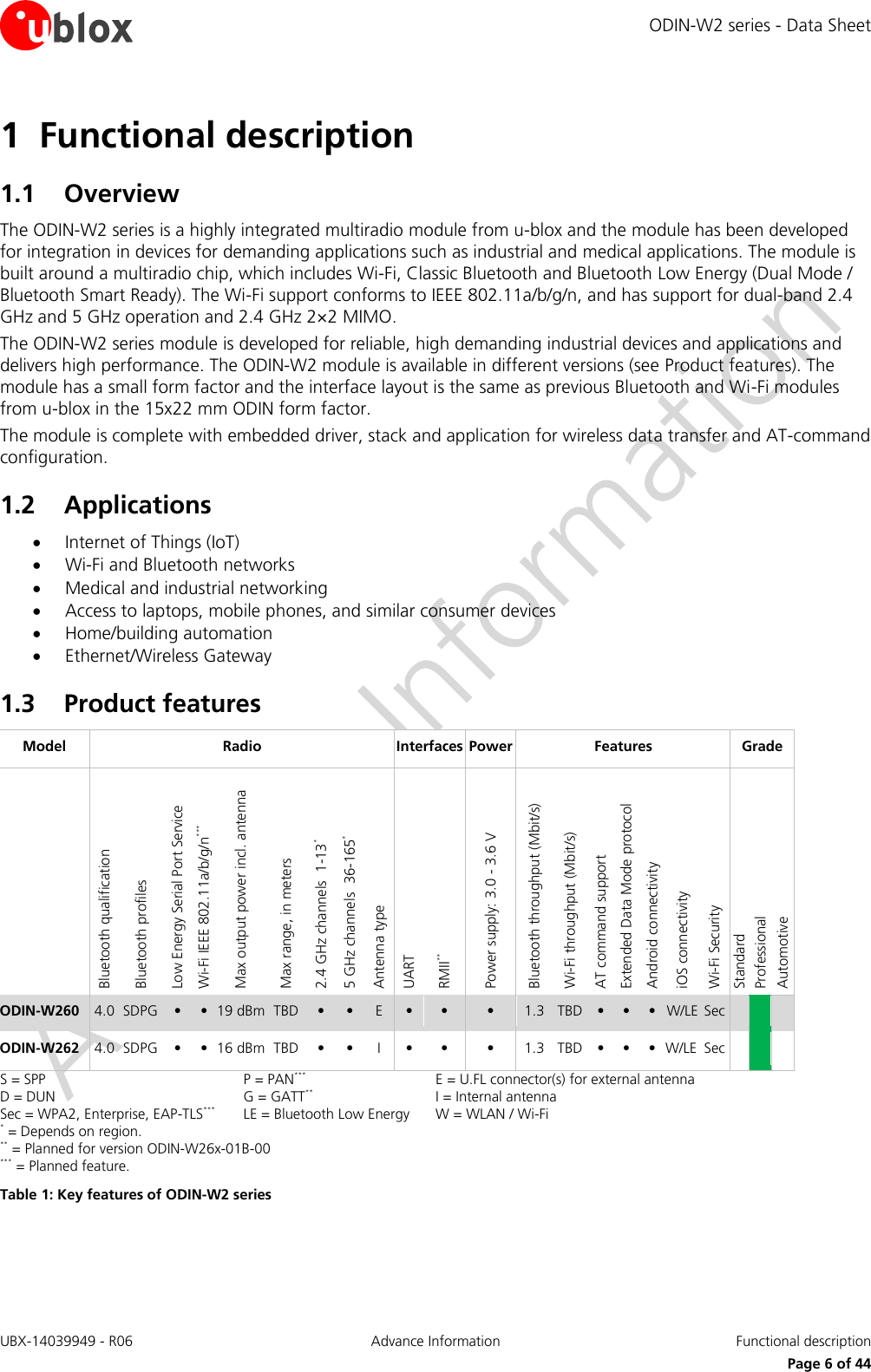
u-blox Malmo AB WLAN and Bluetooth Module ODIN W2 series
UserManual.wiki
>
u blox Malmo
>
0965 User Manual
user manual
Navigation menu
Upload a User Manual
Namespaces
Wiki Guide
HTML
PDF
Info
Views
User Manual
Discussion / Help
Navigation
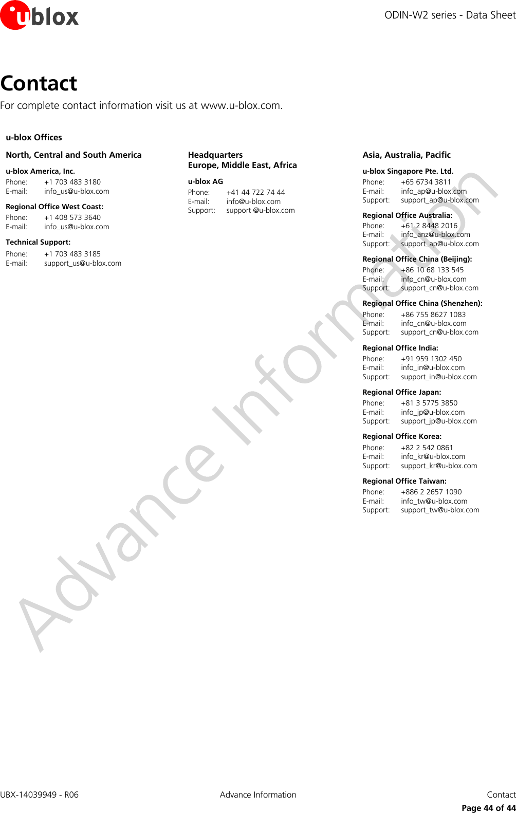
![ODIN-W2 series - Data Sheet UBX-14039949 - R06 Advance Information Functional description Page 8 of 44 1.6 AT command support The ODIN-W2 series modules support AT commands as mentioned in the ODIN-W2 AT Commands Manual [2]. See also the s-center software which is an easy to use tool from u-blox for evaluating, and configuration of u-blox Short Range modules. The s-center tool is available for download on the www.u-blox.com website. 1.7 IEEE 802.11d and additional regulatory domains The ODIN-W2 series module support IEEE 802.11d. IEEE 802.11d is an amendment to the IEEE 802.11 specification that adds support for "additional regulatory domains". IEEE 802.11d allows ODIN-W2 based devices to self-configure and operate according to the regulations of its operating country and includes parameters like country name, channel quantity and maximum transmission level. The country information elements simplifies the creation of 802.11 wireless access points and client devices that meet the different regulations enforced in various parts of the world. 1.7.1 ODIN-W2 IEEE 802.11d implementation description When ODIN-W2 is used as a Wi-Fi station the scan is used to detect which regulatory domain it is currently in. Passive scan is used for channels that are not available in all regulatory domains. The device supports three domains: WORLD, FCC and ETSI where WORLD is the considered all channels that are supported both by FCC, ETSI and most other countries in the world. See Table 3 for which channels are supported in the different regulatory domains. The state transition diagram Figure 2 below describes the algorithm for selecting the current regulatory domain. Figure 2: ODIN-W2 series IEEE 802.11d state transition diagram. Initial regulatory domain is WORLD. At start up a scan is initiated to detect beacons containing country information IEs. If at least one scan result contains country information indicating FCC and no country information indicates ETSI the regulatory domain is set to FCC. If at least three scan results contain country information indicating ETSI and no country information indicates FCC then the regulatory domain is set to ETSI. If the scan result contains country information indicating both FCC and country information indicating ETSI then the regulatory domain is set to WORLD. In the state transition diagram this is the state WORLD_FINAL. This state will not be exited until the device is reset. WORLD FCC WORLD-FINAL ETSI Scan complete FCC AP found and no ETSI AP found Scan complete ETSI found Scan complete Three or more ETSI AP found and no FCC AP found Scan complete FCC found Scan complete No or both FCC and ETSI AP found Entry start scan Do start scan every hour](https://usermanual.wiki/u-blox-Malmo/0965/User-Guide-2819882-Page-8.png)
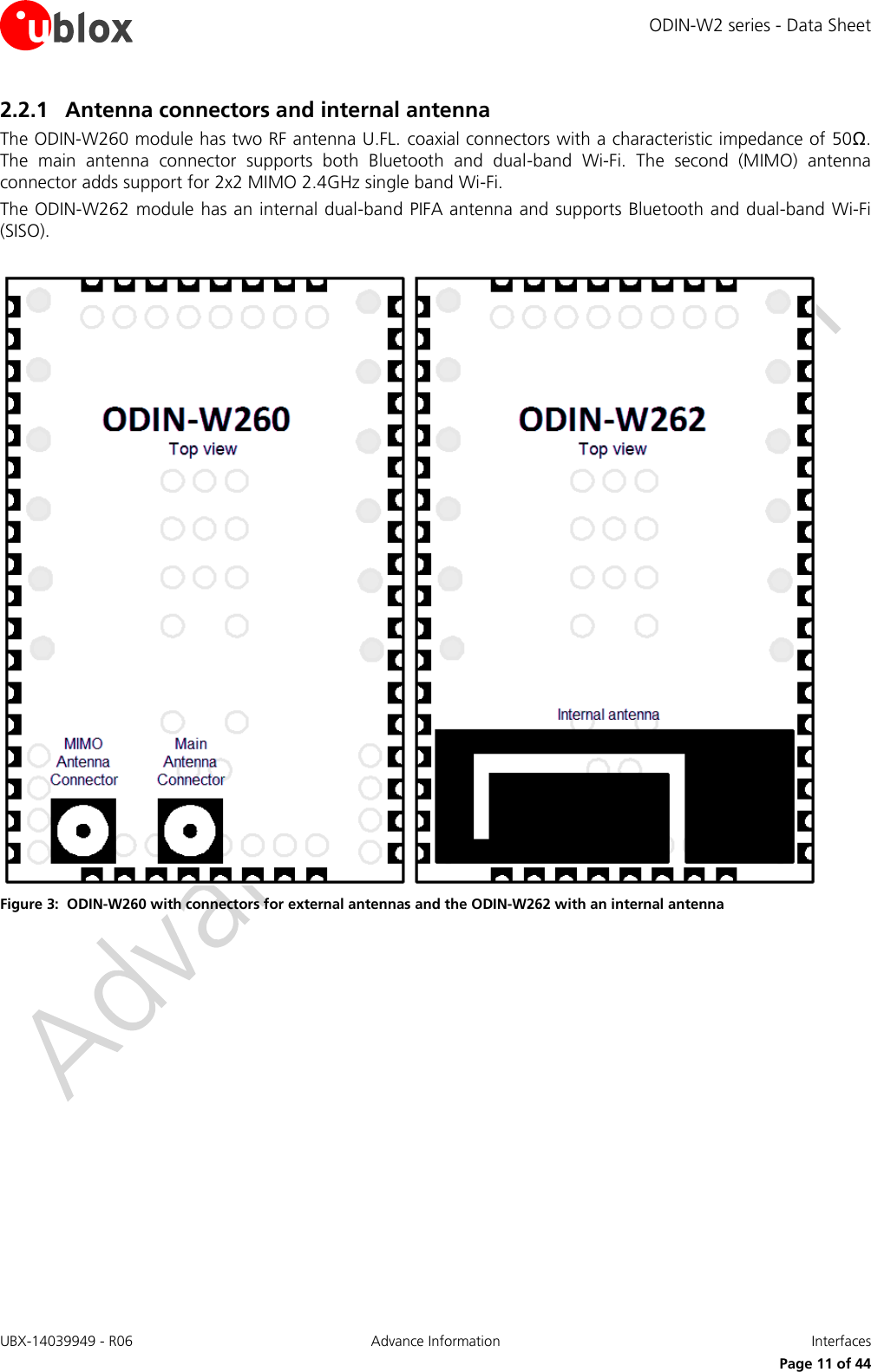
![ODIN-W2 series - Data Sheet UBX-14039949 - R06 Advance Information Interfaces Page 12 of 44 2.3 Data communication interfaces The ODIN-W2 series provides several data communication interfaces which are described below. 2.3.1 UART interface The ODIN-W2 series modules include a 6-wire UART for communication with an application host processor (AT commands, Data communication and firmware upgrades). The following UART signals are available: Data lines (RXD as input, TXD as output) Hardware flow control lines (CTS as input, RTS as output) Link status (DTR as output, DSR as input) It is recommended to use CMOS compatible signal levels. See ODIN-W2 AT Commands Manual [2] and ODIN-W2 series System Integration Manual [2] for more information about the UART interface. 2.3.2 Ethernet interface Support for Ethernet interface is planned for version ODIN-W26x-01B-00. The ODIN-W2 series modules include an integrated Ethernet MAC to communicate with other networked nodes over a shared medium. It supports 10/100 Mbit/s communication and can operate in both full- and half-duplex (CSMA/CD). The Ethernet interface includes: RMII either for MAC to PHY or Ethernet MAC to MAC communication. SMI for PHY configuration The IO voltage of the ODIN-W2 is 1.8 V, which means that the RMII interface operates outside the RMII specification v1.2. If the RMII is to be connected to a PHY circuit, then that circuit must support 1.8 V operation. If a direct RMII to RMII connection is used, then a level shifter might be needed depending on the selected host. The selected hardware setup must be verified on the application board to guarantee operation. 2.3.2.1 RMII The RMII use 7 signals in total. The interface requires an external 50 MHz clock source either from a compatible PHY chip or an external oscillator. The ODIN-W2 module cannot provide this clock signal by itself. 2.3.2.2 SMI (MDC/MDIO management interface) The two-wire SMI is used to configure the PHY chips. It uses a clock line and a data line to clock data to and from the PHY chips registers.](https://usermanual.wiki/u-blox-Malmo/0965/User-Guide-2819882-Page-12.png)
![ODIN-W2 series - Data Sheet UBX-14039949 - R06 Advance Information System functions Page 13 of 44 3 System functions 3.1 Module power modes Support for power save mode is available in version ODIN-W26x-01B-00. The ODIN-W2 series module does not have an internal low power oscillator (LPO) which is required for low power modes. An external 32.768kHz LPO signal can be supplied externally via the LPO_CLK pin if low power modes are required. 3.2 Module reset The ODIN-W2 series modules can be reset (rebooted) in one of the following ways: Low level on the RESET_N pin, which is normally set high by an internal pull-up. This causes a “hardware” reset of the module. The RESET_N line should be driven by an open drain, open collector or contact switch. Using a reset AT command (see the ODIN-W2 AT Commands Manual [2]). This causes an “software” reset of the module. 3.3 System IO The module has the following six different configurable IOs that can be used to indicate different system states or to be used as inputs, thus setting the module in different states: SWITCH_0 RED GREEN/SWITCH_1 BLUE UART_DTR UART_DSR See Pin definition section for more information on the separate IOs. For more information on the use and configuration of the System IOs, see the ODIN-W2 AT Commands Manual [2].](https://usermanual.wiki/u-blox-Malmo/0965/User-Guide-2819882-Page-13.png)
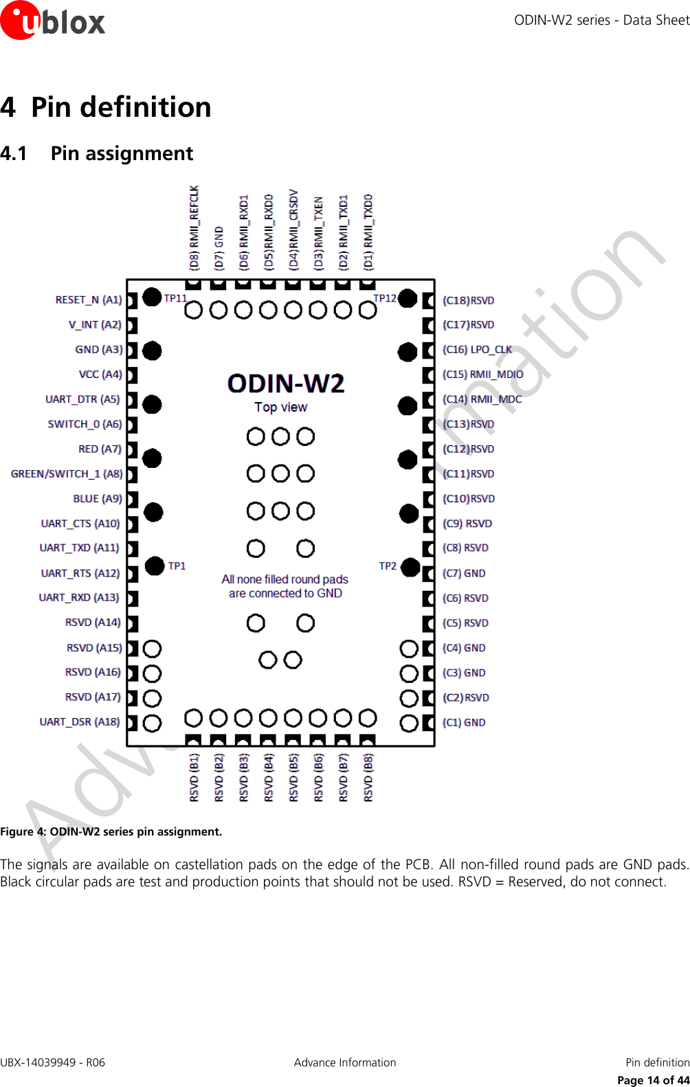
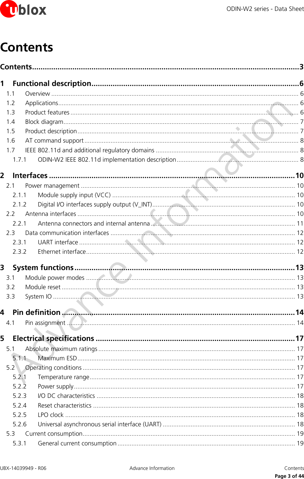
![ODIN-W2 series - Data Sheet UBX-14039949 - R06 Advance Information Pin definition Page 15 of 44 No Name I/O Description Remarks A1 RESET_N I External reset input. Internal active pull-up to V_INT. A2 V_INT O Regulated output of the internal I/O voltage. 1.8V, maximum output current 100mA. The maximum output current can be limited by the internal current consumption of the V_INT rail. See the Current consumption section for current consumption figures. A3 GND N/A Ground All GND pads must be connected to ground. A4 VCC I Module power supply. 3.0 - 3.6 V power supply. A5 UART_DTR O UART Data Terminal Ready. Active low. Can also be used as a System IO. See the System IO section for more information. Also see the ODIN-W2 AT Commands Manual [2] for more information about the pin functionality. A6 SWITCH_0 I Connect on external signal. Active low. A secondary function is that the module will restore all factory settings if both the SWITCH_1 and SWITCH_0 signals are low during start up. See the ODIN-W2 AT Commands Manual [2] for more information about the pin functionality. A7 RED O Logic Red LED Signal. Active low. See the System IO section for more information. Also see the ODIN-W2 AT Commands Manual [2] for more information about the pin functionality. A8 GREEN/ SWITCH_1 O/I This signal is multiplexed: GREEN: Logic Green LED Signal. SWITCH_1: Default Serial Settings. Active low. The GREEN signal is not valid until 500ms after startup. See the System IO section for more information. If the level on this pin is pulled-down during start-up the unit goes back to default serial settings. The SWITCH_1 input is only active during the first 500ms after startup. The module will restore all factory settings if both the SWITCH_1 and SWITCH_0 signals are low during start up. Also see the ODIN-W2 AT Commands Manual [2] for more information about the pin functionality. A9 BLUE O Logic Blue LED Signal. Active low. See the System IO section for more information. Also see the ODIN-W2 AT Commands Manual [2] for more information about the pin functionality. A10 UART_CTS I UART Clear To Send, Hardware flow control. Active low. A11 UART_TXD O UART Transmit. A12 UART_RTS O UART Request To Send, Hardware flow control. Active low. A13 UART_RXD I UART Receive. A14 RSVD N/A Reserved pin. Leave unconnected. A15 RSVD N/A Reserved pin. Leave unconnected. A16 RSVD N/A Reserved pin. Leave unconnected. A17 RSVD N/A Reserved pin. Leave unconnected. A18 UART_DSR I UART Data Set Ready. Active low. Can also be used as a System IO. See the System IO section for more information. Also see the ODIN-W2 AT Commands Manual [2] for more information about the pin functionality. B1 RSVD N/A Reserved pin. Leave unconnected. B2 RSVD N/A Reserved pin. Leave unconnected.](https://usermanual.wiki/u-blox-Malmo/0965/User-Guide-2819882-Page-15.png)
![ODIN-W2 series - Data Sheet UBX-14039949 - R06 Advance Information Electrical specifications Page 19 of 44 5.3 Current consumption These measurements were made while running preliminary firmware (see the product version information on page 2) and are subject to change. No power save functionality is supported yet and especially the idle current consumption will be significantly reduced in coming firmwares. 5.3.1 General current consumption VCC = 3.3 V, TA = 25°C unless otherwise specified. Symbol Parameter Conditions Typ Peak Unit IDD Supply current Reset 5.2 6.0 mA Startup 90 900* mA Idle, not connected, default configuration 90 170 mA Idle, not connected, no running services** 90 120 mA Stop mode*** TBD TBD mA IDD_MAXIMUM Absolute maximum current drain - 1.0 A * Wi-Fi and Bluetooth calibration during the startup phase causes large short current peaks. ** No server running and Bluetooth Connectable and Discoverable turned off. *** Feature not supported in the current firmware version. See [1] for more info. Table 13: General current consumption 5.3.2 Current consumption Wi-Fi 2.4 GHz VCC = 3.3 V, TA = 25°C unless otherwise specified. Symbol Parameter Conditions Typ* Active Typ** Peak*** Unit IDDW24 Supply current not connected Scan, 11 channels, 300 ms 93 380 550 mA Idle, Connected DTIM = 1, Tbeacon = 100 ms 90 350 350 mA Idle, Connected DTIM = 5****, Tbeacon = 100 ms TBD TBD TBD mA IDDW24_TXSISO Supply current SISO transmitting 802.11b 170 350 550 mA 802.11g 180 350 550 mA 802.11n**** TBD TBD TBD mA IDDW24_TXMIMO Supply current 2x2 MIMO transmitting 802.11n**** TBD TBD TBD mA IDDW24_RXSISO Supply current SISO receiving 802.11b 120 - 550 mA 802.11g 106 - 350 mA 802.11n**** TBD TBD TBD mA IDDW24_RXMIMO Supply current 2x2 MIMO receiving 802.11n**** TBD TBD TBD mA * Average during transmission. UART 3 Mbit/s ** Average value for one transmission period. *** Measured maximum at maximum output power. **** Feature not supported in the current firmware version. See [1] for more info. Table 14: Current consumption for Wi-Fi 2.4 GHz](https://usermanual.wiki/u-blox-Malmo/0965/User-Guide-2819882-Page-19.png)
![ODIN-W2 series - Data Sheet UBX-14039949 - R06 Advance Information Electrical specifications Page 20 of 44 5.3.3 Current consumption Wi-Fi 5 GHz VCC = 3.3 V, Tamb = 25°C Symbol Parameter Conditions Typ* Active Typ** Peak*** Unit IDDW5 Supply current not connected Scan, 4 channels, 100 ms 100 400 650 mA Idle, Connected DTIM = 1, Tbeacon = 100 ms 95 400 650 mA Idle, Connected DTIM = 5****, Tbeacon = 100 ms TBD TBD TBD mA IDDW5_TX Supply current SISO transmitting 802.11a 250 400 650 mA 802.11n**** TBD TBD TBD mA IDDW5_RX Supply current SISO receiving 802.11a 102 - 610 mA 802.11n**** TBD TBD TBD mA * Average during transmission. UART 3 Mbit/s ** Average value for one transmission period. *** Measured maximum at maximum output power. **** Feature not supported in the current firmware version. See [1] for more info. Table 15: Current consumption for Wi-Fi 5 GHz 5.3.4 Current consumption Classic Bluetooth VCC = 3.3 V, Tamb = 25°C Symbol Parameter Conditions Typ* Peak** Unit IDDBT_NDNC Supply current not connected Not discoverable, Not connectable 90 100 mA IDDBT_NDC Not discoverable, Connectable, scan interval = TBD, scan window = TBD 90 150 mA IDDBT_DC Discoverable, Connectable, scan interval = TBD, scan window = TBD 90 150 mA IDDBT_INQ Supply current inquiry 105 170 mA IDDBT_IDLE Supply current connected Idle 93 170 mA IDDBT_TX1Mb Transmitting 115 170 mA IDDBT_RX1Mb Receiving 100 150 mA * Average: The cycle mean value for one transmission period. ** Measured at maximum output power. Table 16: Current consumption for classic Bluetooth 5.3.5 Current consumption Bluetooth Low Energy (BLE) VCC = 3.3 V, Tamb = 25°C Symbol Parameter Test conditions Typ* Peak** Unit IDDBLE_CD_NC Supply current not connected Central device Idle 91 150 mA IDDBLE_CD_INQ Low Energy Inquiry, Scan interval = TBD, Scan window = TBD 95 170 mA IDDBLE_PD_NC Peripheral device Idle 90 150 mA IDDBLE_PD_ADV Advertising interval = TBD 90 150 mA IDDBLE_CD_IDLE Supply current connected Central device Idle 92 150 mA IDDBLE_CD_TX Transmitting 95 150 mA IDDBLE_CD_RX Receiving 95 150 mA IDDBLE_PD_IDLE Peripheral device Idle 92 150 mA IDDBLE_PD_TX Transmitting 95 150 mA IDDBLE_PD_RX Receiving 95 150 mA * Average: The cycle mean value for one transmission period. ** Measured at maximum output power. Table 17: Current consumption for Bluetooth Low Energy (BLE)](https://usermanual.wiki/u-blox-Malmo/0965/User-Guide-2819882-Page-20.png)
![ODIN-W2 series - Data Sheet UBX-14039949 - R06 Advance Information Electrical specifications Page 21 of 44 5.4 RF characteristics 5.4.1 Wi-Fi receiver characteristics 2.4 GHz VCC = 3.3 V, Tamb = 25 °C Parameter Test conditions Antenna port Channel / Freq [MHz] IEEE limit Typ* Unit Receive sensitivity SISO 802.11b, Rate = 1 Mbit/s, PER ≤ 8% MAIN port 6 / 2437 -76 -94 dBm 802.11b, Rate = 11 Mbit/s, PER ≤ 8% MAIN port 6 / 2437 -76 -86 dBm 802.11g, Rate = 6 Mbit/s, PER ≤ 10% MAIN port 6 / 2437 -82 -89 dBm 802.11g, Rate = 54 Mbit/s, PER ≤ 10% MAIN port 6 / 2437 -65 -72 dBm 802.11n**, Rate = 6.5 Mbit/s (MCS0), PER ≤ 10% MAIN port 6 / 2437 -82 TBD dBm 802.11n**, Rate = 65 Mbit/s (MCS7), PER ≤ 10% MAIN port 6 / 2437 -64 TBD dBm Receive sensitivity 2x2 MIMO 802.11n**, Rate = 13 Mbit/s (MCS8), PER ≤ 10% MAIN port (stream 1) 6 / 2437 -64 TBD dBm MIMO port (stream 2) 6 / 2437 -64 TBD dBm 802.11n**, Rate = 130 Mbit/s (MCS15), PER ≤ 10% MAIN port (stream 1) 6 / 2437 -64 TBD dBm MIMO port (stream 2) 6 / 2437 -64 TBD dBm * Measured conducted on ODIN-W260, measurement tolerance ±1.0 dB. ** Feature not supported in the current firmware version. See [1] for more info. Table 18: Receiver characteristics for 2.4 GHz Wi-Fi 5.4.2 Wi-Fi receiver characteristics 5 GHz VCC = 3.3 V, Tamb = 25 °C Parameter Test conditions Channel / Freq [MHz] IEEE limit Typ* Unit Receive sensitivity 802.11a, Rate = 6 Mbit/s, PER ≤ 10% 36 / 5180 -82 -85 dBm 100 / 5500 -82 -88 dBm 140 / 5825 -82 -86 dBm 802.11a, Rate = 48 Mbit/s, PER ≤ 10% 36 / 5180 -66 -69 dBm 100 / 5500 -66 -73 dBm 140 / 5825 -66 -71 dBm 802.11n**, Rate = 6.5 Mbit/s (MCS0) , PER ≤ 10% 36 / 5180 -82 TBD dBm 100 / 5500 -82 TBD dBm 140 / 5825 -82 TBD dBm 802.11n**, Rate = 65 Mbit/s (MCS7) , PER ≤ 10% 36 / 5180 -64 TBD dBm 100 / 5500 -64 TBD dBm 140 / 5825 -64 TBD dBm * Measured conducted on ODIN-W260, measurement tolerance ±1.0 dB. ** Feature not supported in the current firmware version. See [1] for more info. Table 19: Receiver characteristics for 5 GHz Wi-Fi](https://usermanual.wiki/u-blox-Malmo/0965/User-Guide-2819882-Page-21.png)
![ODIN-W2 series - Data Sheet UBX-14039949 - R06 Advance Information Electrical specifications Page 22 of 44 5.4.3 Wi-Fi transmitter characteristics 2.4 GHz VCC = 3.3 V, Tamb = 25 °C Parameter Test conditions Antenna port IEEE EVM limit EVM* Typ* Unit Transmitting output power SISO 802.11b, Rate = 1 Mbit/s MAIN port -14 -28 15.2 dBm 802.11b, Rate = 11 Mbit/s MAIN port -14 -26 15.6 dBm 802.11g, Rate = 6 Mbit/s MAIN port -5 -16 15.2 dBm 802.11g, Rate = 54 Mbit/s MAIN port -25 -25 12.3 dBm 802.11n**, Rate = 6.5 Mbit/s (MCS0) MAIN port -5 TBD TBD dBm 802.11n**, Rate = 65 Mbit/s (MCS7) MAIN port -28 TBD TBD dBm Transmitting output power 2x2 MIMO 802.11n**, Rate = 13 Mbit/s (MCS8) MAIN port (stream 1) -5 TBD TBD dBm MIMO port (stream 2) -5 TBD TBD dBm 802.11n**, Rate = 130 Mbit/s (MCS15) MAIN port (stream 1) -28 TBD TBD dBm MIMO port (stream 2) -28 TBD TBD dBm * Measured conducted on ODIN-W260 with max output power, measurement tolerance ±1.0 dB. Regional power limitation can reduce the max output power (especially on channels close to band edges). ** Feature not supported in the current firmware version. See [1] for more info. Table 20: Wi-Fi transmitter characteristics 2.4 GHz 5.4.4 Wi-Fi transmitter characteristics 5 GHz VCC = 3.3 V, Tamb = 25 °C Parameter Test conditions Channel / Freq [MHz] IEEE EVM limit EVM* Typ* Unit Transmitting output power 802.11a, Rate = 6 Mbit/s 40 / 5180 -5 -26 14.2 dBm 100 / 5500 -5 -25 14.1 dBm 140 / 5700 -5 -18 15.1 dBm 802.11a, Rate = 54 Mbit/s 40 / 5180 -25 -26 14.2 dBm 100 / 5500 -25 -25 14.1 dBm 140 / 5700 -25 -25 14.7 dBm 802.11n**, Rate = 6.5 Mbit/s (MCS0) 40 / 5180 -5 TBD TBD dBm 100 / 5500 -5 TBD TBD dBm 140 / 5700 -5 TBD TBD dBm 802.11n**, Rate = 65 Mbit/s (MCS7) 40 / 5180 -28 TBD TBD dBm 100 / 5500 -28 TBD TBD dBm 140 / 5700 -28 TBD TBD dBm * Measured conducted on ODIN-W260 with max output power, measurement tolerance ±1.0 dB. Regional power limitation can reduce the max output power (especially on channels close to band edges). ** Feature not supported in the current firmware version. See [1] for more info. Table 21: Wi-Fi transmitter characteristics 5 GHz 5.4.5 Bluetooth classic receiver characteristics VCC = 3.3 V, Tamb = 25 °C Parameter Test conditions Limit Typ* Min* Unit Rx sensitivity BR 1Mbit, GFSK, BER ≤ 0.1% -70 -89 dBm EDR 2Mbit, π/4-DQPSK, BER ≤ 0.007% -70 -90 dBm EDR 3Mbit, 8DPSK , BER ≤ 0.007% -70 -83 dBm Maximum input level BR 1Mbit, GFSK, BER ≤ 0.1% -20 -6 dBm EDR 2Mbit, π/4-DQPSK, BER ≤ 0.1% -20 -10 dBm EDR 3Mbit, 8DPSK , BER ≤ 0.1% -20 -10 dBm * Measured conducted on ODIN-W260, measurement tolerance ±1.0 dB. Table 22: Bluetooth classic receiver sensitivity](https://usermanual.wiki/u-blox-Malmo/0965/User-Guide-2819882-Page-22.png)
![ODIN-W2 series - Data Sheet UBX-14039949 - R06 Advance Information Qualification and approvals Page 32 of 44 7.5 Japan Radio Equipment Compliance The ODIN-W2 module complies with the Japanese Technical Regulation Conformity Certification of Specified Radio Equipment (ordinance of MPT N°. 37, 1981), Article 2, Paragraph 1: Item 19 "2.4 GHz band wide band low power data communication system" Item 19-3 “Low power data communications system in the 5.2/5.3 GHz band” Item 19-3-2 “Low power data communications system in the 5.6 GHz band” The ODIN-W2 module is restricted on the Japanese market to be used indoors only if the product is operating in the 5.2/5.3 GHz band. The information: “Indoor use only” translated into Japanese (この製品は屋内においてのみ使用可能です) must be visible: on the certified end product. on the product package in which the end product is marketed. in the users / installation manual of the end product. The indoor usage information is recommended to be printed close to the Giteki mark but it is also permitted to place that information on another prominent position. The ODIN-W2 MIC certification number is 204-510009. The very small size of the module makes it not reasonable to fit the GITEKI mark and certification number onto the module label. Instead the Giteki mark and certification number is available in this document, the ODIN-W2 series System Integration Manual [2] and on the ODIN-W2 package. When a product integrated with an ODIN-W2 module is placed on the Japanese market, either must: the ODIN-W2 module be affixed with a label with the Giteki marking below. In this case is it recommended that the product is marked with “Contains MIC ID: R 204-510009”. the product be affixed with a label with the Giteki marking below. The marking must be visible for inspection. 204-510009 この製品は屋内においてのみ使用可能です Figure 7: Giteki mark, R and the ODIN-W2 MIC certification number. The “Indoor use only” information translated into Japanese below is mandatory if the product is operating in the 5.2/5.3 GHz band. The recommended size of the Giteki mark is Ø5.0 mm but the minimum size is Ø3.0 mm. The end product holder should also include a copy of the Japan Radio Certificate to the end product technical documentation. See the Contact information in the end of this document for a copy of the Radio Certificate. 7.6 Bluetooth qualification information The ODIN-W2 series modules have been qualified according to the Bluetooth 4.0 specification.](https://usermanual.wiki/u-blox-Malmo/0965/User-Guide-2819882-Page-32.png)
![ODIN-W2 series - Data Sheet UBX-14039949 - R06 Advance Information Qualification and approvals Page 33 of 44 For information how to List and Declare your product see the ODIN-W2 series System Integration Manual [2]. Please note that the ODIN-W2 series module is Bluetooth qualified as TBD - QD ID TBD. This means that you do not need to do any further qualification.](https://usermanual.wiki/u-blox-Malmo/0965/User-Guide-2819882-Page-33.png)
![ODIN-W2 series - Data Sheet UBX-14039949 - R06 Advance Information Product handling and soldering Page 38 of 44 9 Product handling and soldering 9.1 Packaging The ODIN-W2 series modules are delivered as hermetically sealed, reeled tapes to enable efficient production, production lot set-up and tear-down. For more information about packaging, see the u-blox Package Information Guide [3]. 9.1.1 Reels The ODIN-W2 series modules are delivered on the reel as described in Table 27: Parameter Specification Reel type B2 Delivery quantity 200 Table 27: Reel information for ODIN-W2 series modules 9.1.2 Tapes Figure 8 shows the position and the orientation of ODIN-W2 modules as they are delivered on the tape, while Figure 9 specifies the tape dimensions. Figure 8: Orientation for ODIN-W2 modules on tape](https://usermanual.wiki/u-blox-Malmo/0965/User-Guide-2819882-Page-38.png)
![ODIN-W2 series - Data Sheet UBX-14039949 - R06 Advance Information Product handling and soldering Page 39 of 44 Figure 9: ODIN-W2 series tape dimensions 9.2 Moisture sensitivity levels The ODIN-W2 series modules are Moisture Sensitive Devices (MSD) in accordance with the IPC/JEDEC specification. The Moisture Sensitivity Level (MSL) relates to the required packaging and handling precautions. The ODIN-W2 series modules are rated at MSL level 4. For more information regarding moisture sensitivity levels, labeling, and storage, see the u-blox Package Information Guide [3]. For MSL standards, see IPC/JEDEC J-STD-020, which can be downloaded from www.jedec.org. 9.3 Reflow soldering Reflow profiles are to be selected according to u-blox recommendations (see ODIN-W2 series System Integration Manual [2]). Failure to observe these recommendations can result in severe damage to the device. 9.4 ESD precautions The ODIN-W2 series modules contain highly sensitive electronic circuitry and are Electrostatic Sensitive Devices (ESD). Handling the ODIN-W2 series modules without proper ESD protection may destroy or damage them permanently. The ODIN-W2 series modules are electrostatic sensitive devices (ESD) and require special ESD precautions typically applied to ESD sensitive components. The Maximum ESD section reports the maximum ESD ratings of the ODIN-W2 series modules. Proper ESD handling and packaging procedures must be applied throughout the processing, handling and operation of any application that incorporates the ODIN-W2 series module. The ESD precautions should be implemented on the application board where the module is mounted as described in the ODIN-W2 series System Integration Manual [2]. Failure to observe these recommendations can result in severe damage to the device.](https://usermanual.wiki/u-blox-Malmo/0965/User-Guide-2819882-Page-39.png)
![ODIN-W2 series - Data Sheet UBX-14039949 - R06 Advance Information Labeling and ordering information Page 41 of 44 10.2 Explanation of codes Three different product code formats are used. The Product Name is used in documentation such as this data sheet and identifies all u-blox products, independent of packaging and quality grade. The Ordering Code includes options and quality, while the Type Number includes the hardware and firmware versions. Table 29 below details these three different formats: Format Structure Product Name PPPP-TGRV Ordering Code PPPP -TGRV-TTQ Type Number PPPP -TGRV-TTQ-XX Table 29: Product code formats Table 30 explains the parts of the product code. Code Meaning Example PPPP Form factor ODIN TG Platform (Technology and Generation) T – Dominant technology, For example, W: Wi-Fi, B: Bluetooth G - Generation W2: Wi-Fi Generation 2 R Wireless technology; range [0...9] 6: Multi-radio dual-band 2.4+5GHz V Variant based on the same platform; range [00…99] 0: default mounting, with connector for external antenna TT Major Product Version 00: first revision Q Quality grade A: Automotive B: Professional C: Standard B: professional grade XX Minor product version (not relevant for certification) Default value is 00 Table 30: Part identification code 10.3 Ordering information Ordering Code Product ODIN-W260-00B Wi-Fi IEEE802.11a/b/g/n (dual-band) 2.4 GHz 2x2 MIMO and Bluetooth dual-mode module with dual U.FL. coaxial antenna connectors. ODIN-W262-00B Wi-Fi IEEE802.11a/b/g/n (dual-band) and Bluetooth dual-mode module with internal dual-band antenna. Table 31: Product ordering codes](https://usermanual.wiki/u-blox-Malmo/0965/User-Guide-2819882-Page-41.png)
![ODIN-W2 series - Data Sheet UBX-14039949 - R06 Advance Information Related documents Page 43 of 44 Related documents [1] ODIN-W2 AT Commands Manual, document number UBX-14044127 [2] ODIN-W2 series System Integration Manual, document number UBX-14040040 [3] u-blox Package Information Guide, document number UBX-14001652 For regular updates to u-blox documentation and to receive product change notifications please register on our homepage. Revision history Revision Date Name Status / Comments R01 05-Sep-2014 mwej Initial release R02 16-Feb-2015 fbro Minor updates R03 23-Apr-2015 ajoh Updated features list, added input from early measurements and label specification R04 08-July-2015 fbro, kgom Updated and moved to MS word format R05 07-Sept-2015 mwej Major updated with after review: - Major text updates. - Some IO voltage levels updated. - Mechanical outline clarified and some tolerances updated. - Updated performance measurements with ODIN-W26x SPA FW v0.11.05 - Updated after type approval with approval information. R06 09-Nov-2015 mwej Antenna section added and text about indoor restrictions added.](https://usermanual.wiki/u-blox-Malmo/0965/User-Guide-2819882-Page-43.png)