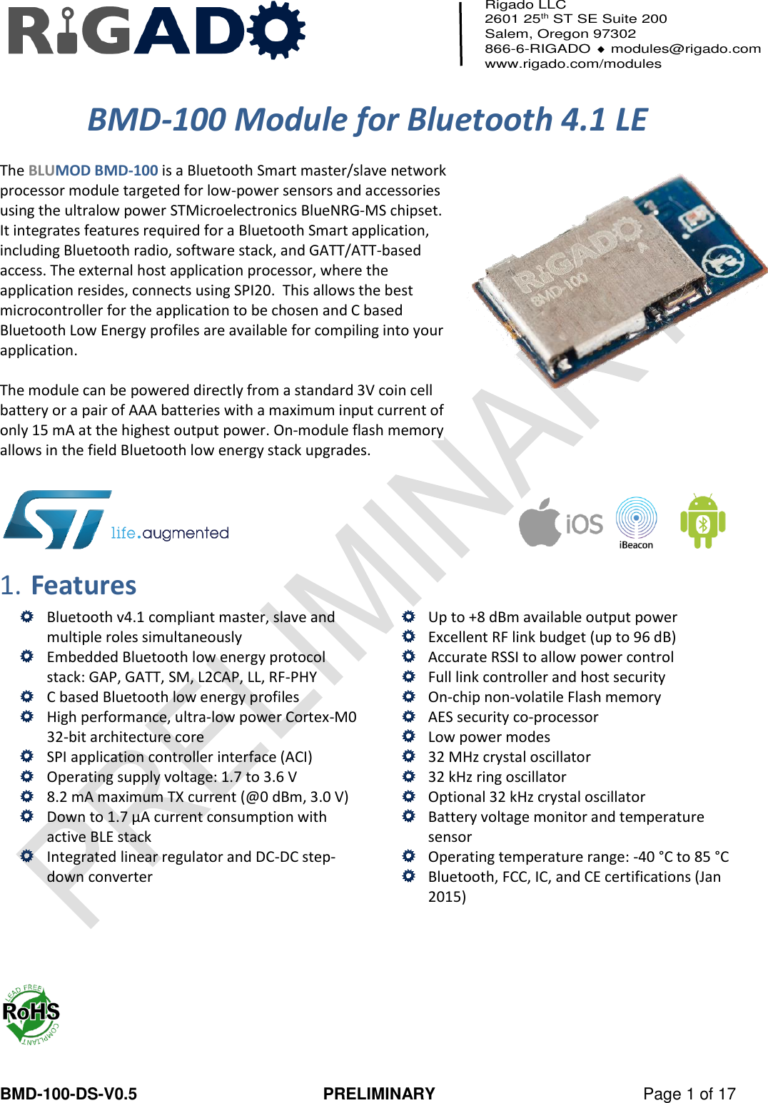
u blox 02 BMD-100 User Manual BMD 100

Rigado LLC BMD-100 BMD 100

User Manual

  BMD-100-DS-V0.5  PRELIMINARY  Page 1 of 17 Rigado LLC 2601 25th ST SE Suite 200 Salem, Oregon 97302 866-6-RIGADO  modules@rigado.com www.rigado.com/modules     BMD-100 Module for Bluetooth 4.1 LE  The BLUMOD BMD-100 is a Bluetooth Smart master/slave network processor module targeted for low-power sensors and accessories using the ultralow power STMicroelectronics BlueNRG-MS chipset.  It integrates features required for a Bluetooth Smart application, including Bluetooth radio, software stack, and GATT/ATT-based access. The external host application processor, where the application resides, connects using SPI20.  This allows the best microcontroller for the application to be chosen and C based Bluetooth Low Energy profiles are available for compiling into your application.   The module can be powered directly from a standard 3V coin cell battery or a pair of AAA batteries with a maximum input current of only 15 mA at the highest output power. On-module flash memory allows in the field Bluetooth low energy stack upgrades.      1. Features  Bluetooth v4.1 compliant master, slave and multiple roles simultaneously  Embedded Bluetooth low energy protocol stack: GAP, GATT, SM, L2CAP, LL, RF-PHY  C based Bluetooth low energy profiles  High performance, ultra-low power Cortex-M0 32-bit architecture core  SPI application controller interface (ACI)  Operating supply voltage: 1.7 to 3.6 V  8.2 mA maximum TX current (@0 dBm, 3.0 V)  Down to 1.7 μA current consumption with active BLE stack  Integrated linear regulator and DC-DC step-down converter   Up to +8 dBm available output power  Excellent RF link budget (up to 96 dB)  Accurate RSSI to allow power control  Full link controller and host security  On-chip non-volatile Flash memory  AES security co-processor  Low power modes  32 MHz crystal oscillator  32 kHz ring oscillator  Optional 32 kHz crystal oscillator  Battery voltage monitor and temperature sensor  Operating temperature range: -40 °C to 85 °C  Bluetooth, FCC, IC, and CE certifications (Jan 2015)
BMD-100 Module Datasheet Bluetooth 4.1 LE 1/5/2014 BMD-100-DS-V0.5  PRELIMINARY  Page 2 of 17 2. Ordering Information Email modules@rigado.com for quotes and ordering or visit www.rigado.com/bmd-100  Part Number Description BMD-100-A-R BMD-100 module, Rev A, Tape & Reel BMD-100-A-CT BMD-100 module, Rev A, Cut Tape BMD-100-NUCL BMD-100 Nucleo Shield BMD-100-EVAL BMD-100 Evaluation Kit (Nucleo Shield + Nucleo Platform) Table 1 - Ordering Part Numbers 3. Hardware Block Diagram  Figure 1 – Hardware Block Diagram 4. Software Block Diagram  Figure 2 – Software Block Diagram
BMD-100 Module Datasheet Bluetooth 4.1 LE 1/5/2014 BMD-100-DS-V0.5  PRELIMINARY  Page 3 of 17 Table of Contents 1. FEATURES .................................................................................................................................................................. 1 2. ORDERING INFORMATION ........................................................................................................................................ 2 3. HARDWARE BLOCK DIAGRAM ................................................................................................................................... 2 4. SOFTWARE BLOCK DIAGRAM .................................................................................................................................... 2 5. QUICK SPECIFICATIONS ............................................................................................................................................. 4 6. PIN DESCRIPTIONS .................................................................................................................................................... 5 7. ELECTRICAL SPECIFICATIONS ..................................................................................................................................... 6 7.1. ABSOLUTE MAXIMUM RATINGS ................................................................................................................................ 6 7.2. OPERATING CONDITIONS .......................................................................................................................................... 6 7.3. SPI INTERFACE ........................................................................................................................................................... 6 7.4. CLOCKS ....................................................................................................................................................................... 6 7.5. NOTE .......................................................................................................................................................................... 7 8. APPLICATION CONTROLLER INTERFACE ..................................................................................................................... 7 9. MECHANICAL DATA ................................................................................................................................................... 8 9.1. MODULE DIMENSIONS .............................................................................................................................................. 8 9.2. RECOMMENDED PCB LAND PAD ............................................................................................................................... 8 10. MODULE MARKING ................................................................................................................................................. 9 11. RF DESIGN NOTES.................................................................................................................................................... 9 11.1. RECOMMENDED RF LAYOUT & GROUND PLANE..................................................................................................... 9 11.2. MECHANICAL ENCLOSURE ..................................................................................................................................... 10 11.3. ANTENNA PATTERN ............................................................................................................................................... 10 11.3.1. S33 SMITH CHART ........................................................................................................................................... 10 11.3.2. 3D RADIATION PATTERN ................................................................................................................................. 10 11.3.3. XY-PLANE ......................................................................................................................................................... 10 11.3.4. XZ-PLANE ......................................................................................................................................................... 10 11.3.5. YZ-PLANE ......................................................................................................................................................... 10 12. EVALUATION BOARDS ........................................................................................................................................... 10 13. CUSTOM DEVELOPMENT ....................................................................................................................................... 11 14. BLUETOOTH CERTIFICATION .................................................................................................................................. 11 15. REGULATORY STATEMENTS .................................................................................................................................. 12 15.1. FCC STATEMENT: ................................................................................................................................................... 12 15.2. FCC IMPORTANT NOTES: ....................................................................................................................................... 12 15.3. IC STATEMENT: ...................................................................................................................................................... 13 15.4. IC IMPORTANT NOTES: .......................................................................................................................................... 13 15.5. CE REGULATORY: ................................................................................................................................................... 14 16. SOLDER REFLOW TEMPERATURE-TIME PROFILE .................................................................................................... 15 17. PACKAGING AND LABELING .................................................................................................................................. 15 17.1. CARRIER TAPE DIMENSIONS .................................................................................................................................. 15 17.2. REEL PACKAGING ................................................................................................................................................... 15 17.3. PACKAGING LABEL ................................................................................................................................................. 15 18. CAUTIONS ............................................................................................................................................................. 16 19. LIFE SUPPORT POLICY ............................................................................................................................................ 16 20. DOCUMENT HISTORY ............................................................................................................................................ 16 21. RELATED DOCUMENTS .......................................................................................................................................... 17
BMD-100 Module Datasheet Bluetooth 4.1 LE 1/5/2014 BMD-100-DS-V0.5  PRELIMINARY  Page 4 of 17 5. Quick Specifications Bluetooth Version 4.1 (Bluetooth Smart) Peripheral & Central Security AES-128 LE connections up to 8   Radio Frequency 2.402GHz to 2.480GHz Modulation GFSK at 1 Mbps Transmit power +8 dBm Receiver sensitivity -88 dBm (BLE mode) Antenna  Integrated ceramic chip   Current Consumption TX only @ +8 dBm, 4 dBm, 2 dBm 15.1 mA, 10.9 mA, 8.2 mA RX only 7.7 mA CPU, Flash and RAM on/off 3.3 mA, 2.0 mA Sleep, 32kHz XO/RO 2.4 µA, 3.5 µA Standby, (RAM2 Off) 1.3 µA Reset 5 nA   Dimensions Length 13.6 mm Width 8.4 mm Height 1.8 mm   Hardware Interface ACI over SPI with IRQ and Reset (8 MHz Max) Power supply 1.7V to 3.6V   Planned Certifications (Jan 2015) FCC FCC part 15 modular qualification – FCC ID: 2AA9B03 IC Industry Canada RSS-210 modular qualification – IC: 12208A-01 CE EN 60950-1: 2011-01   3.1 (a) : Health and Safety of the User  EN 301 489-17 V2.2.1  3.1 (b) : Electromagnetic Compatibility  EN 300 328 V1.8.1              3.2 : Effective use of spectrum allocated Bluetooth Component (Tested) – DID: TBD Table 2- Quick Specifications
BMD-100 Module Datasheet Bluetooth 4.1 LE 1/5/2014 BMD-100-DS-V0.5  PRELIMINARY  Page 5 of 17 6. Pin Descriptions  Figure 3- Pin out (Top View) Pin description Pin Name Direction Description 14 SPI_CS In  SPI slave select = SPI enable. 17 SPI_CLK  In SPI clock (max 8 MHz). 16 SPI_MOSI In Master output, slave input. 15 SPI_MISO Out Master input, slave output. 18 SPI_IRQ Out Slave has data for master. 13 nRESET In Reset and deep sleep control 10 SXTAL0 In 32 kHz Crystal (optional) 12 SXTAL1 In 32 kHz Crystal (optional) 19 VCC Pwr +1.7 to +3.6VDC input 1 A,B,C,D,E,F,7,9,20 GND Pwr Electrical Ground 1,2,3,11 RESERVED N/A Connect to Ground 4,5,6,8 RESERVED N/A Leave Unconnected  Table 3 – Pin Descriptions Note 1: An external capacitor for VCC is not strictly required, however a 1µF - 4.7µF ceramic capacitor is recommended.
BMD-100 Module Datasheet Bluetooth 4.1 LE 1/5/2014 BMD-100-DS-V0.5  PRELIMINARY  Page 6 of 17 7. Electrical Specifications 7.1. Absolute Maximum Ratings Symbol Parameter Min. Max. Unit VCC_MAX Voltage on supply pin -0.3 3.9 V VIO_MAX Voltage on SXTAL pins -0.3 1.4 V TS Storage Temperature Range -40 125 °C VESD-HBM Electrostatic discharge voltage -2.0 2.0 kV Table 4 – Absolute Maximum Ratings 7.2. Operating Conditions Symbol Parameter Min. Max. Unit VCC Operating supply voltage 1.7 3.6 V TA Operating Ambient Temperature Range -40 85 °C Table 5 – Operating Conditions 7.3. SPI Interface The application controller interface (ACI) uses a standard SPI slave interface as the transport Layer on five physical wires:  2 control wires (clock and slave select)  2 data wires with serial shift-out (MOSI and MISO) in full duplex  1 wire to indicate data availability from the slave   All the SPI pins have an internal pull-down except for the SPI_CS that has a pull-up. All the SPI pins, except the SPI_CS, are in high impedance state during the low-power states. The SPI_IRQ pin requires an external pull-down resistor.  Symbol Parameter Min. Typ. Max. Unit FMAX SPI Clock Max Frequency   8 MHz TRISE Rise Time 5 - 19 ns TFALL Fall Time 6 - 22 ns VIH Input High Voltage 0.65 x VCC - VCC V VIL Input Low Voltage VSS - 0.35 x VCC V VOH Output High Voltage (Vcc = 3.3V) 2.4 - - V VOL Output Low Voltage (Vcc = 3.3V) - - 0.4 V RPU Pull-up Resistance 11 13 16 kΩ RPD Pull-down Resistance 11 13 16 kΩ Table 6 – SPI Interface 7.4. Clocks The BMD-100 integrates two low-speed frequency oscillators (LSOSC) and two high-speed  (32 MHz) frequency oscillators (HSOSC).
BMD-100 Module Datasheet Bluetooth 4.1 LE 1/5/2014 BMD-100-DS-V0.5  PRELIMINARY  Page 7 of 17 The primary high frequency clock is a 32 MHz crystal oscillator. There is also a fast starting 12 MHz ring oscillator that provides the clock while the crystal oscillator is starting up. Frequency tolerance of the high-speed crystal is ±30 ppm. The low frequency clock is used in Low Power mode and can be supplied either by a 32.7kHz oscillator that uses an external crystal and guarantees up to ±50 ppm frequency tolerance, or by a ring oscillator with maximum ±500 ppm frequency tolerance, which does not require any external components.    32.768 kHz Crystal Specification Requirements Symbol Parameter Typ. Max. Unit fnom Crystal frequency 32.768 - kHz Ftol,BLE Frequency tolerance - ±50 ppm PD Load Capacitance - 0.1 μW Table 7 - 32.768 kHz Crystal 32.768 kHz Oscillator Comparison Symbol Parameter Typ. Max. Unit fnom Crystal frequency 37.4 - kHz Ftol,BLE Frequency tolerance - ±500 ppm Table 8 - 32.768 kHz Oscillator 7.5. Note Additional electrical characteristics and current consumption data can be found on the BlueNRG-MS datasheet provided by STMicroelectronics at www.st.com.  8. Application controller interface The application controller interface is based on a standard SPI module with transfer rates up to 8 Mbits/s. The application controller Interface defines a software protocol providing functions to access all the services offered by the layers of the embedded Bluetooth stack. The ACI commands are described in the BlueNRG-MS ACI command interface document provided by STMicroelectronics at www.st.com.
BMD-100 Module Datasheet Bluetooth 4.1 LE 1/5/2014 BMD-100-DS-V0.5  PRELIMINARY  Page 8 of 17 9. Mechanical Data  9.1. Module Dimensions   Figure 4- Module Dimensions (All dimensions are in mm) 9.2. Recommended PCB Land Pad  Figure 5- Module Dimensions
BMD-100 Module Datasheet Bluetooth 4.1 LE 1/5/2014 BMD-100-DS-V0.5  PRELIMINARY  Page 9 of 17 (All dimensions are in mm) 10. Module Marking  Figure 6 – Module Marking – Rev A  11. RF Design Notes 11.1. Recommended RF Layout & Ground Plane The integrated ceramic chip antenna requires a suitable ground plane to radiate effectively. Reducing the ground plane from that shown in figure 7 will reduce the effective radiated power. The BMD-100 module should be placed at the edge of the ground plane with the antenna side towards the edge. Place a copper keep-out under the antenna (area shown in red). The area under the keep-out and extending out from the edge of the ground plane should be kept clear of copper and other metal. The BMD-100 uses a Johanson Technology 2450AT07A0100 chip antenna.  Additional information on the antenna can be acquired from www.johansontechnology.com.
BMD-100 Module Datasheet Bluetooth 4.1 LE 1/5/2014 BMD-100-DS-V0.5  PRELIMINARY  Page 10 of 17  Figure 7- Recommended RF Layout 11.2. Mechanical Enclosure Care should be taken when designing and placing the module into an enclosure. Metal should be kept clear from the antenna area, both above and below. Any metal around the module can negatively impact RF performance.  The module is designed and tuned for the antenna and RF components to be in free air. Any potting, epoxy fill, plastic overmolding, or conformal coating can negatively impact RF performance and must be evaluated by the customer. 11.3. Antenna Pattern TBD. 11.3.1. S33 Smith Chart TBD. 11.3.2. 3D Radiation Pattern TBD. 11.3.3. XY-plane TBD.  11.3.4. XZ-plane TBD. 11.3.5. YZ-plane TBD. 12. Evaluation Boards Rigado has developed a Nucleo-compatible shield for the BMD-100 that provides a complete development solution for Bluetooth 4.1 LE.
BMD-100 Module Datasheet Bluetooth 4.1 LE 1/5/2014 BMD-100-DS-V0.5  PRELIMINARY  Page 11 of 17 13. Custom Development Project specific firmware and hardware for the BMD-100 can be created or modified for customers.   Custom embedded development is available upon request.  Please contact Rigado at info@rigado.com or 1-866-6-RIGADO for custom engineering options and fees. 14. Bluetooth Certification TBD.
BMD-100 Module Datasheet Bluetooth 4.1 LE 1/5/2014 BMD-100-DS-V0.5  PRELIMINARY  Page 12 of 17  15. Regulatory Statements 15.1. FCC Statement: This device has been tested and found to comply with part 15 of the FCC rules. These limits are designed to provide reasonable protection against harmful interference in a residential installation. This equipment generates, uses and can radiate radio frequency energy and, if not installed and used in accordance with the instructions, may cause harmful interference to radio communications. However, there is no guarantee that interference will not occur in a particular installation. If this equipment does cause harmful interference to radio or television reception, which can be determined by turning the equipment off and on, the user is encouraged to try to correct the interference by one or more of the following measures:  Reorient or relocate the receiving antenna.  Increase the separation between the equipment and the receiver  Connect the equipment into an outlet on a circuit different from that to which the receiver is connected.  Consult the dealer or an experienced radio/TV technician for help.  Operation is subjected to the following two conditions: (1) This device may no cause harmful interference, and (2) this device must accept any interference received, including interference that may cause undesired operation. Note: Modification to this product will void the user’s authority to operate this equipment.  Note: Modification to this product will void the users’ authority to operate this equipment. 15.2. FCC Important Notes: (1) FCC Radiation Exposure Statement This equipment complies with FCC RF radiation exposure limits set forth for an uncontrolled environment. This transmitter must not be co-located or operating in conjunction with any other antenna or transmitter. This equipment complies with Part 15 of the FCC Rules. Operation is subject the following two conditions:  (1) This device may not cause harmful interference, and (2) This device must accept any interference received, including interference that may cause undesired operation.   The devices must be installed and used in strict accordance with the manufacturer’s instructions as described in the user documentation that comes with the product.  Caution! The manufacturer is not responsible for any radio or TV interference caused by unauthorized modifications to this equipment. Such modification could void the user authority to operate the equipment.  (2) Co-location Warning: This device and its antenna(s) must not be co-located or operating in conjunction with any other antenna or transmitter.  (3) OEM integration instructions: This device is intended only for OEM integrators under the following conditions:  The transmitter module may not be co-located with any other transmit or antenna. The module shall be only used with the integral antenna(s) that has been originally tested and certified with this module.
BMD-100 Module Datasheet Bluetooth 4.1 LE 1/5/2014 BMD-100-DS-V0.5  PRELIMINARY  Page 13 of 17  As long as the two (2) conditions above are met, further transmitter testing will not be required. However, the OEM integrator is still responsible for testing their end-product for any additional compliance requirements with this module installed (for example, digital device emission, PC peripheral requirements, etc.)  (4) OEM integration instructions: In the event that these conditions cannot be met (for example certain laptop configuration or co-location with another transmitter), then the FCC authorization for this module in combination with the host equipment is no longer considered valid and the FCC ID of the module cannot be used on the final product. In these and circumstance, the OEM integrator will be responsible for re-evaluating the end product (including the transmitter) and obtaining a separate FCC authorization.  (5) End product labeling: The final end product must be labeled in a visible area with the following: “Contains FCC ID: 2AA9B02”.  Any similar wording that expresses the same meaning may be used.   The FCC Statement below should also be included on the label. When not possible, the FCC Statement should be included in the User Manual of the host device.  “This device complies with part 15 of the FCC rules.  Operation is subject to the following two conditions. (1) This device may not cause harmful interference. (2) This device must accept any interference received, including interference that may cause undesired operation. “  (6) Information that must be placed in the end user manual: The OEM integrator has to be aware not to provide information to the end user regarding how to install or remove this RF module in the user’s manual of the end product which integrates this module. The end user manual shall include all required regulatory information/warning as show in this manual. 15.3. IC Statement: This device complies with Industry Canada licence-exempt RSS standard(s). Operation is subject to the following two conditions: (1) this device may not cause interference, and (2) this device must accept any interference, including interference that may cause undesired operation of the device.   Le présent appareil est conforme aux CNR d'Industrie Canada applicables aux appareils radio exempts de licence. L'exploitation est autorisée aux deux conditions suivantes : (1) l'appareil ne doit pas produire de brouillage, et (2) l'utilisateur de l'appareil doit accepter tout brouillage radioélectrique subi, même si le brouillage est susceptible d'en compromettre le fonctionnement.   RF exposure warning: The equipment complies with RF exposure limits set forth for an uncontrolled environment. The antenna(s) used for this transmitter must not be co-located or operating in conjunction with any other antenna or transmitter.   Avertissement d'exposition RF: L'équipement est conforme aux limites d'exposition aux RF établies pour un incontrôlés environnement. L'antenne (s) utilisée pour ce transmetteur ne doit pas être co-localisés ou onctionner en conjonction avec toute autre antenne ou transmetteur .  15.4. IC Important Notes: 1. The OEM integrator has to be aware not to provide information to the end user regarding how to install or remove this RF module in the user manual of the end product.
BMD-100 Module Datasheet Bluetooth 4.1 LE 1/5/2014 BMD-100-DS-V0.5  PRELIMINARY  Page 14 of 17 The user manual provided by OEM integrators for end users must include the following information in a prominent location.  2. To comply with IC RF exposure compliance requirements, the antenna used for this transmitter must not be co‐located or operating in conjunction with any other antenna or transmitter, except in accordance with IC multi‐transmitter product procedures.  3. The final system integrator must ensure there is no instruction provided in the user manual or customer documentation indicating how to install or remove the transmitter module except such device has implemented two‐ways authentication between module and the host system.  4. The host device shall be properly labeled to identify the module within the host device. The final end product must be labeled in a visible area with the following: “Contains IC: 12208A-02”.  Any similar wording that expresses the same meaning may be used.   The IC Statement below should also be included on the label. When not possible, the IC Statement should be included in the User Manual of the host device.  “This device complies with Industry Canada licence-exempt RSS standard(s). Operation is subject to the following two conditions: (1) this device may not cause interference, and (2) this device must accept any interference, including interference that may cause undesired operation of the device.   Le présent appareil est conforme aux CNR d'Industrie Canada applicables aux appareils radio exempts de licence. L'exploitation est autorisée aux deux conditions suivantes : (1) l'appareil ne doit pas produire de brouillage, et (2) l'utilisateur de l'appareil doit accepter tout brouillage radioélectrique subi, même si le brouillage est susceptible d'en compromettre le onctionnement.” 15.5. CE Regulatory: This device has been tested and has been found to be complaint against the following standards. OEM integrators should consult with qualified test house to verify all regulatory requirements have been met for their complete device. From Directive 2006/95/EC:  EN 60950-1: 2006 + A11: 2009 + A1: 2010 + A12: 2011 From R&TTE Directive 1999/5/EC:  ETSI EN 300 440-1 V 1.6.1  ETSI EN 300 440-2 V 1.4.1   EN 62479:2010 From Directive 2004/108/EC:  ETSI EN 301 489-3 V1.6.1   ETSI EN 301 489-1 V1.9.2 Declarations of Conformity and supporting test reports are available upon request.
BMD-100 Module Datasheet Bluetooth 4.1 LE 1/5/2014 BMD-100-DS-V0.5  PRELIMINARY  Page 15 of 17 16. Solder Reflow Temperature-Time Profile  Figure 8 - Reflow Profile for Lead Free Solder 17. Packaging and Labeling 17.1. Carrier Tape Dimensions TBD. 17.2. Reel Packaging TBD. 17.3. Packaging Label  Figure 9 – Packaging Label
BMD-100 Module Datasheet Bluetooth 4.1 LE 1/5/2014 BMD-100-DS-V0.5  PRELIMINARY  Page 16 of 17 18. Cautions 1) The guidelines of this document should be followed in order to assure proper performance of the module. 2) This product is for use in office, business, and residential applications, but not medical devices. 3) This module may short-circuit. If a short circuit can result in serious damage or injury then failsafe precautions should be used. This could be accomplished by redundant systems and protection circuits. 4) Supply voltage to the module should not be higher than the specified inputs or reversed. Additionally it should not contain noise, spikes, or AC ripple voltage. 5) Avoid use with other high frequency circuits. 6) Use methods to eliminate static electricity when working with the module as it can damage the components. 7) Contact with wires, the enclosure, or any other objects should be avoided. 8) Refer to the recommended pattern when designing for this module. 9) If hand soldering is used, be sure to use the precautions outlined in this document. 10) This module should be kept away from heat, both during storage and after installation. 11) Do not drop or physically shock the module. 12) Do not damage the interface surfaces of the module. 13) The module should not be mechanically stressed at any time (storage, handling, installation). 14) Do not store or expose this module to:  Humid or salty air conditions  High concentrations of corrosive gasses.  Long durations of direct sunlight.  Temperatures lower than -40°C or higher than 125°C. 19. Life Support Policy This product is not designed to be used in a life support device or system, or in applications where there is potential for a failure or malfunction to, directly or indirectly, cause significant injury. By using this product in an application that poses these risks, such as described above, the customer is agreeing to indemnify Rigado for any damages that result. 20. Document History Revision Date Changes / Notes 0.5 1/5/14 Initial Release - Preliminary
BMD-100 Module Datasheet Bluetooth 4.1 LE 1/5/2014 BMD-100-DS-V0.5  PRELIMINARY  Page 17 of 17  21. Related Documents STMicroelectronics Documents:  DM00141263: BlueNRG-MS Datasheet

Navigation menu