u blox 1EHQ37NN UMTS/GSM//LTE Data Module User Manual TOBY L4 series
u-blox AG UMTS/GSM//LTE Data Module TOBY L4 series
u blox >
Contents
- 1. TempConfidential_TOBY-L4_SysIntegrManual_UBX-16024839
- 2. TempConfidential_TOBY-L4_SysIntegrManual_UBX-16024839_rev1
TempConfidential_TOBY-L4_SysIntegrManual_UBX-16024839
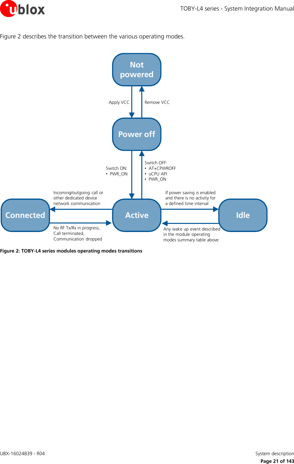
![TOBY-L4 series - System Integration Manual UBX-16024839 - R04 System description Page 7 of 143 1 System description 1.1 Overview The TOBY-L4 series modules support multi-band LTE-FDD, LTE-TDD, DC-HSPA+, and (E)GPRS radio access technologies (see Table 1) in the very small TOBY 248-pin LGA form-factor (35.6 x 24.8 mm), which is easy to integrate in compact designs. TOBY-L4 series modules are form-factor compatible with the other u-blox cellular module families (including SARA, LISA, LARA, and TOBY form-factors): this allows customers to take maximum advantage of their hardware and software investments, and provides very short time-to-market. With LTE-Advanced carrier aggregation category 6 data rates up to 301.5 Mbit/s (downlink) / 51.0 Mbit/s (uplink), the modules are ideal for applications requiring the highest data-rates and high-speed internet access. Reduced cost variants supporting LTE Cat 4 or LTE Cat 1 will be available for lower speed or “pure” telematics devices. TOBY-L4 series include the following LTE Cat 6 modules with 3G and 2G fallback: TOBY-L4006 modules, mainly designed for operation in North America TOBY-L4106 modules, mainly designed for operation in Europe TOBY-L4206 modules, mainly designed for operation in Asia-Pacific and South America TOBY-L4906 modules, mainly designed for operation in China TOBY-L4 series modules include the following product versions: The “00” product versions, integrating the u-blox uCPU on-chip processor to allow customers to run their dedicated applications on an embedded Linux distribution based on Yocto, with RIL-Core connectivity APIs The “50” product versions, which can be controlled by an external application processor through standard and u-blox proprietary AT commands described in the u-blox AT Commands Manual [2] TOBY-L4 series modules are the ideal product for the development of all kinds of automotive devices, such as smart antennas and in-dash telematics / infotainment devices, supporting a comprehensive set of HW interfaces (including RGMII/RMII for Ethernet and analog audio) over a very extended temperature range that allow the establishment of an emergency call up to +95 °C, complemented by a set of state-of-the art security features. TOBY-L4 series modules are also the perfect choice for consumer fixed-wireless terminals, mobile routers and gateways, applications requiring video streaming and many other industrial (M2M) applications. TOBY-L4 series modules are manufactured in ISO/TS 16949 certified sites, with the highest production standards and the highest quality and reliability. Each module is fully tested and inspected during production. The modules are qualified according to the automotive requirements as for systems installed in vehicles.](https://usermanual.wiki/u-blox/1EHQ37NN.TempConfidential-TOBY-L4-SysIntegrManual-UBX-16024839/User-Guide-3759877-Page-7.png)
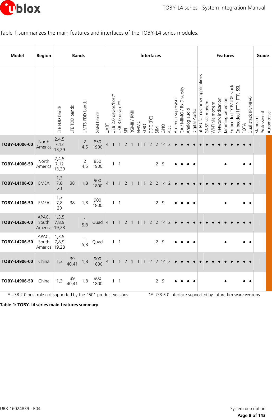
![TOBY-L4 series - System Integration Manual UBX-16024839 - R04 System description Page 9 of 143 TOBY-L4 series modules provide multi-band 4G / 3G / 2G multi-mode radio access technologies, based on the 3GPP Release 10 protocol stack, with the main characteristics summarized in Table 2 and Table 3. LTE 3G 2G LTE-Advanced Carrier Aggregation Frequency Division Duplex (LTE FDD) Time Division Duplex (LTE TDD) Down-Link CA / MIMO / Rx diversity Dual-Cell High Speed Packet Access Frequency Division Duplex (UMTS FDD) Down-Link Rx diversity Enhanced Data rate GSM Evolution (EDGE) Time Division Multiple Access (TDMA) DL Advanced Rx Performance Phase 1 LTE FDD Power Class Class 3 (23 dBm) LTE TDD Power Class Class 3 (23 dBm) UMTS FDD Power Class Class 3 (24 dBm) GMSK Power Class Class 4 (33 dBm) for GSM/E-GSM bands Class 1 (30 dBm) for DCS/PCS bands 8-PSK Power Class Class E2 (27 dBm) for GSM/E-GSM bands Class E2 (26 dBm) for DCS/PCS bands Data rate LTE category 6: up to 301.5 Mbit/s DL up to 51.0 Mbit/s UL Data rate FDD UE categories: DL cat.24, up to 42.2 Mbit/s UL cat.6, up to 5.76 Mbit/s Data rate GPRS multi-slot class 33, CS1-CS4: up to 107.0 kbit/s DL up to 85.6 kbit/s UL EDGE multi-slot class 33, MCS1-MCS9 up to 296.0 kbit/s DL up to 236.8 kbit/s UL Table 2: TOBY-L4 series LTE, 3G and 2G characteristics summary Module Region LTE FDD bands LTE TDD bands LTE CA UMTS FDD bands GSM bands TOBY-L4006 North America 12 (700 MHz) 17 (700 MHz) 29 (700 MHz) 13 (750 MHz) 5 (850 MHz) 4 (1700 MHz) 2 (1900 MHz) 7 (2600 MHz) 4 + 17 2 + 13 2 + 17 2 + 29 4 + 5 4 + 4 4 + 13 4 + 29 5 (850 MHz) 4 (1700 MHz) 2 (1900 MHz) GSM 850 PCS 1900 TOBY-L4106 EMEA, APAC 20 (800 MHz) 8 (900 MHz) 3 (1800 MHz) 1 (2100 MHz) 7 (2600 MHz) 38 (2600 MHz) 3 + 20 7 + 20 3 + 3 3 + 7 8 (900 MHz) 1 (2100 MHz) E-GSM 900 DCS 1800 TOBY-L4206 APAC, South America 28 (750 MHz) 19 (850 MHz) 5 (850 MHz) 8 (900 MHz) 9 (1800 MHz) 3 (1800 MHz) 1 (2100 MHz) 7 (2600 MHz) 3 + 28 3 + 7 7 + 28 3 + 3 1 + 8 3 + 19 1 + 19 5 (850 MHz) 8 (900 MHz) 1 (2100 MHz) GSM 850 E-GSM 900 DCS 1800 PCS 1900 TOBY-L4906 China 3 (1800 MHz) 1 (2100 MHz) 39 (1900 MHz) 40 (2300 MHz) 41 (2500 MHz) 3 + 3 40 + 40 41 + 41 39 + 41 8 (900 MHz)1 1 (2100 MHz) E-GSM 900 DCS 1800 Table 3: TOBY-L4 series supported bands2 and Carrier Aggregation combinations summary 1 Down-Link Rx diversity not supported on this band 2 TOBY-L4 series modules support all the E-UTRA channel bandwidths for each operating band according to 3GPP TS 36.521-1 [13].](https://usermanual.wiki/u-blox/1EHQ37NN.TempConfidential-TOBY-L4-SysIntegrManual-UBX-16024839/User-Guide-3759877-Page-9.png)
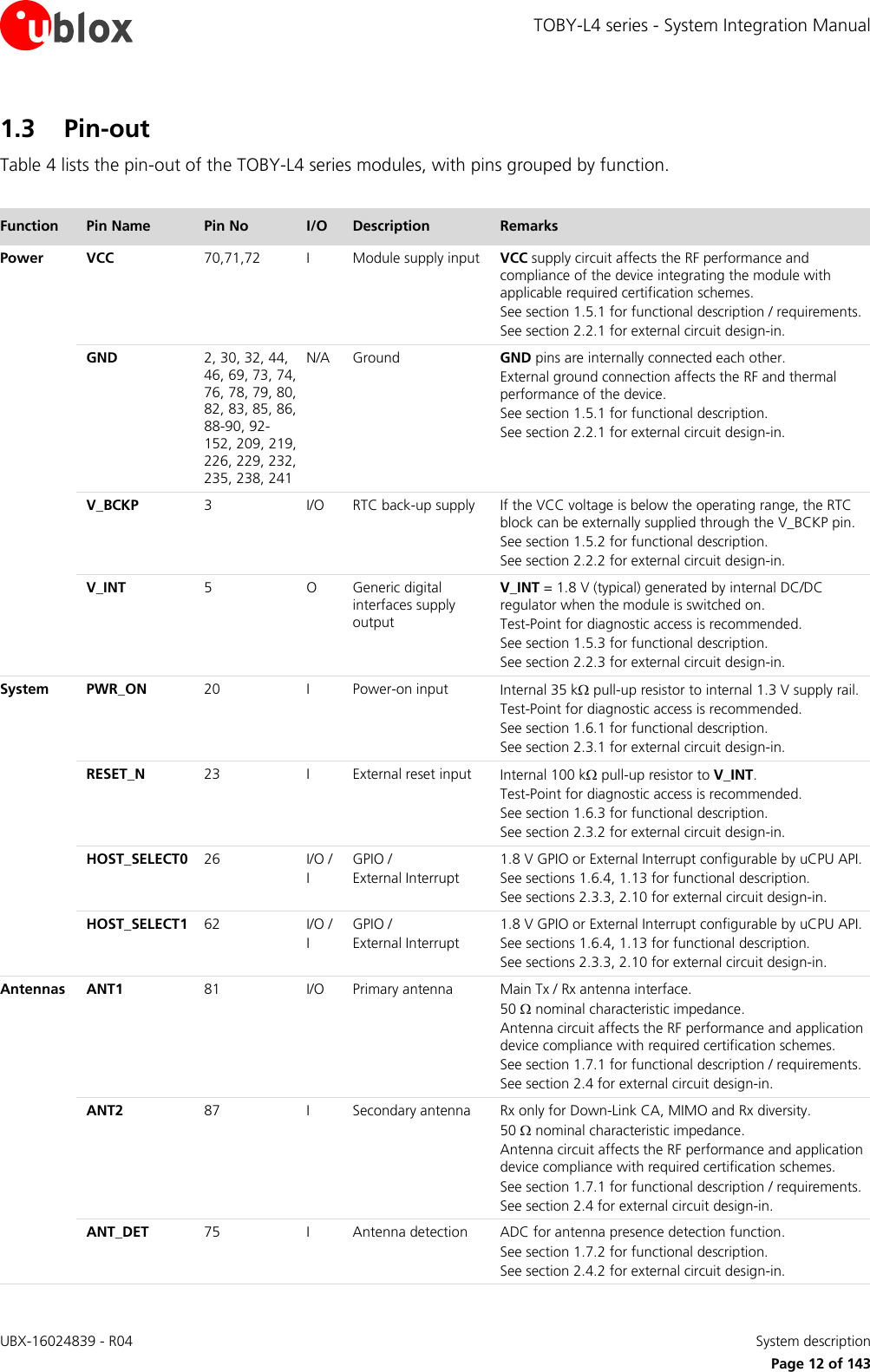
![TOBY-L4 series - System Integration Manual UBX-16024839 - R04 System description Page 13 of 143 Function Pin Name Pin No I/O Description Remarks SIM0 VSIM 59 O SIM0 supply output VSIM = 1.8 V / 3 V output as per the connected SIM type. See section 1.8 for functional description. See section 2.5 for external circuit design-in. SIM_IO 57 I/O SIM0 data Data input/output for 1.8 V / 3 V SIM. Internal 4.7 k pull-up to VSIM. See section 1.8 for functional description. See section 2.5 for external circuit design-in. SIM_CLK 56 O SIM0 clock 3.9 MHz clock output for 1.8 V / 3 V SIM. See section 1.8 for functional description. See section 2.5 for external circuit design-in. SIM_RST 58 O SIM0 reset Reset output for 1.8 V / 3 V SIM. See section 1.8 for functional description. See section 2.5 for external circuit design-in. SIM1 VSIM1 172 O SIM1 supply output VSIM1 = 1.8 V / 3 V output as per the connected SIM type. See section 1.8 for functional description. See section 2.5 for external circuit design-in. SIM1_IO 178 I/O SIM1 data Data input/output for 1.8 V / 3 V SIM. Internal 4.7 k pull-up to VSIM1. See section 1.8 for functional description. See section 2.5 for external circuit design-in. SIM1_CLK 182 O SIM1 clock 3.9 MHz clock output for 1.8 V / 3 V SIM. See section 1.8 for functional description. See section 2.5 for external circuit design-in. SIM1_RST 177 O SIM1 reset Reset output for 1.8 V / 3 V SIM. See section 1.8 for functional description. See section 2.5 for external circuit design-in. USB VUSB_DET 4 I USB detect input VBUS (5 V typical) generated by the host must be connected to this pin to enable the module USB device interface. Test-Point for diagnostic / FW update access is recommended. See section 1.9.1 for functional description. See section 2.6.1 for external circuit design-in. USB_D– 27 I/O USB High-Speed 2.0 diff. transceiver (–) 90 nominal differential impedance (Z0). 30 nominal common mode impedance (ZCM). Pull-up or pull-down resistors and external series resistors as required by the USB 2.0 specifications [3] are part of the USB pin driver and need not be provided externally. Test-Point for diagnostic / FW update access is recommended. See section 1.9.1 for functional description. See section 2.6.1 for external circuit design-in. USB_D+ 28 I/O USB High-Speed 2.0 diff. transceiver (+) 90 nominal differential impedance (Z0). 30 nominal common mode impedance (ZCM). Pull-up or pull-down resistors and external series resistors as required by the USB 2.0 specifications [3] are part of the USB pin driver and need not be provided externally. Test-Point for diagnostic / FW update access is recommended. See section 1.9.1 for functional description. See section 2.6.1 for external circuit design-in. USB_ID 168 I USB device identification Pin for ID resistance measurement. See section 1.9.1 for functional description. See section 2.6.1 for external circuit design-in.](https://usermanual.wiki/u-blox/1EHQ37NN.TempConfidential-TOBY-L4-SysIntegrManual-UBX-16024839/User-Guide-3759877-Page-13.png)
![TOBY-L4 series - System Integration Manual UBX-16024839 - R04 System description Page 14 of 143 Function Pin Name Pin No I/O Description Remarks USB_SSTX+ 175 O USB Super-Speed 3.0 diff. transmitter (+) 90 nominal differential characteristic impedance. Internal series 100 nF capacitor for AC coupling. Compliant with USB Revision 3.0 specification [4]. See section 1.9.1 for functional description. See section 2.6.1 for external circuit design-in. USB_SSTX– 176 O USB Super-Speed 3.0 diff. transmitter (–) 90 nominal differential characteristic impedance. Internal series 100 nF capacitor for AC coupling. Compliant with USB Revision 3.0 specification [4]. See section 1.9.1 for functional description. See section 2.6.1 for external circuit design-in. USB_SSRX+ 170 I USB Super-Speed 3.0 diff. receiver (+) 90 nominal differential characteristic impedance. Compliant with USB Revision 3.0 specification [4]. See section 1.9.1 for functional description. See section 2.6.1 for external circuit design-in. USB_SSRX– 171 I USB Super-Speed 3.0 diff. receiver (–) 90 nominal differential characteristic impedance. Compliant with USB Revision 3.0 specification [4]. See section 1.9.1 for functional description. See section 2.6.1 for external circuit design-in. UART0 RXD 17 O UART0 data output 1.8 V output, Circuit 104 (RXD) in ITU-T V.24. Test-Point for diagnostic access recommended. See section 1.9.2 for functional description. See section 2.6.2 for external circuit design-in. TXD 16 I UART0 data input 1.8 V input, Circuit 103 (TXD) in ITU-T V.24. Internal active pull-up to V_INT. Test-Point for diagnostic access recommended. See section 1.9.2 for functional description. See section 2.6.2 for external circuit design-in. CTS 15 O UART0 clear to send output 1.8 V output, Circuit 106 (CTS) in ITU-T V.24. See section 1.9.2 for functional description. See section 2.6.2 for external circuit design-in. RTS 14 I UART0 ready to send input 1.8 V input, Circuit 105 (RTS) in ITU-T V.24. Internal active pull-up to V_INT. See section 1.9.2 for functional description. See section 2.6.2 for external circuit design-in. DSR 10 I/O / I GPIO / External Interrupt 1.8 V GPIO or External Interrupt configurable by uCPU API. See sections 1.9.2, 1.13 for functional description. See sections 2.6.1, 2.10 for external circuit design-in. RI 11 O / I/O / I UART0 ring indicator / GPIO / External Interrupt 1.8 V output, Circuit 125 (RI) in ITU-T V.24. Configurable as GPIO or External Interrupt. See sections 1.9.2, 1.13 for functional description. See sections 2.6.1, 2.10 for external circuit design-in. DTR 13 I/O / I GPIO / External Interrupt 1.8 V GPIO or External Interrupt configurable by uCPU API. See sections 1.9.2, 1.13 for functional description. See sections 2.6.1, 2.10 for external circuit design-in. DCD 12 I/O / I GPIO / External Interrupt 1.8 V GPIO or External Interrupt configurable by uCPU API. See sections 1.9.2, 1.13 for functional description. See sections 2.6.1, 2.10 for external circuit design-in.](https://usermanual.wiki/u-blox/1EHQ37NN.TempConfidential-TOBY-L4-SysIntegrManual-UBX-16024839/User-Guide-3759877-Page-14.png)
![TOBY-L4 series - System Integration Manual UBX-16024839 - R04 System description Page 16 of 143 Function Pin Name Pin No I/O Description Remarks I2C1 SCL1 54 O I2C1 clock 1.8 V open drain. External pull-up required. See section 1.9.4 for functional description. See section 2.6.4 for external circuit design-in. SDA1 55 I/O I2C1 data 1.8 V open drain. External pull-up required. See section 1.9.4 for functional description. See section 2.6.4 for external circuit design-in. SDIO SDIO_D0 66 I/O SDIO serial data [0] SDIO interface for communication with Wi-Fi / Bluetooth. See section 1.9.5 for functional description. See section 2.6.5 for external circuit design-in. SDIO_D1 68 I/O SDIO serial data [1] SDIO interface for communication with Wi-Fi / Bluetooth. See section 1.9.5 for functional description. See section 2.6.5 for external circuit design-in. SDIO_D2 63 I/O SDIO serial data [2] SDIO interface for communication with Wi-Fi / Bluetooth. See section 1.9.5 for functional description. See section 2.6.5 for external circuit design-in. SDIO_D3 67 I/O SDIO serial data [3] SDIO interface for communication with Wi-Fi / Bluetooth. See section 1.9.5 for functional description. See section 2.6.5 for external circuit design-in. SDIO_CLK 64 O SDIO serial clock SDIO interface for communication with Wi-Fi / Bluetooth. See section 1.9.5 for functional description. See section 2.6.5 for external circuit design-in. SDIO_CMD 65 I/O SDIO command SDIO interface for communication with Wi-Fi / Bluetooth. See section 1.9.5 for functional description. See section 2.6.5 for external circuit design-in. Ethernet V_ETH 221 O Ethernet Interface supply output Ethernet (RGMII / RMII) interface supply output. See section 1.9.6 for functional description. See section 2.6.6 for external circuit design-in. ETH_TX_CLK 29 O Ethernet Transmission Clock RGMII: Transmit reference clock (TXC). RMII: Reference clock (REF_CLK). See section 1.9.6 for functional description. See section 2.6.6 for external circuit design-in. ETH_TX_CTL 33 O Ethernet Transmit Control RGMII: Control signal for the transmit data (TXEN on TXC rising edge; TXEN xor TXER on TXC falling edge). RMII: Control signal for the transmit data (TX_EN). See section 1.9.6 for functional description. See section 2.6.6 for external circuit design-in. ETH_TXD0 37 O Ethernet Transmit Data [0] RGMII: Tx data bit 0 / 4 on TXC rising / falling edges. RMII: Tx data bit 0 in sync with REF_CLK. See section 1.9.6 for functional description. See section 2.6.6 for external circuit design-in. ETH_TXD1 36 O Ethernet Transmit Data [1] RGMII: Tx data bit 1 / 5 on TXC rising / falling edges. RMII: Tx data bit 1 in sync with REF_CLK. See section 1.9.6 for functional description. See section 2.6.6 for external circuit design-in. ETH_TXD2 35 O Ethernet Transmit Data [2] RGMII: Tx data bit 2 / 6 on TXC rising / falling edges. RMII: Not used. See section 1.9.6 for functional description. See section 2.6.6 for external circuit design-in. ETH_TXD3 34 O Ethernet Transmit Data [3] RGMII: Tx data bit 3 / 7 on TXC rising / falling edges. RMII: Not used. See section 1.9.6 for functional description. See section 2.6.6 for external circuit design-in.](https://usermanual.wiki/u-blox/1EHQ37NN.TempConfidential-TOBY-L4-SysIntegrManual-UBX-16024839/User-Guide-3759877-Page-16.png)
![TOBY-L4 series - System Integration Manual UBX-16024839 - R04 System description Page 17 of 143 Function Pin Name Pin No I/O Description Remarks ETH_RX_CLK 43 I Ethernet Receive Clock RGMII: Receive reference clock (RXC). RMII: Not used. See section 1.9.6 for functional description. See section 2.6.6 for external circuit design-in. ETH_RX_CTL 42 I Ethernet Receive Control RGMII: Control signal for receive data (RXDV on RXC rising edge; RXDV xor RXER on RXC falling edge). RMII: Control signal for receive data, contains carrier sense (CRS) and data valid (RX_DV) information. See section 1.9.6 for functional description. See section 2.6.6 for external circuit design-in. ETH_RXD0 38 I Ethernet Receive Data [0] RGMII: Rx data bit 0 / 4 on RXC rising / falling edges. RMII: Rx data bit 0 in sync with REF_CLK. See section 1.9.6 for functional description. See section 2.6.6 for external circuit design-in. ETH_RXD1 39 I Ethernet Receive Data [1] RGMII: Rx data bit 1 / 5 on RXC rising / falling edges. RMII: Rx data bit 1 in sync with REF_CLK. See section 1.9.6 for functional description. See section 2.6.6 for external circuit design-in. ETH_RXD2 40 I Ethernet Receive Data [2] RGMII: Rx data bit 2 / 6 on RXC rising / falling edges. RMII: Not used. See section 1.9.6 for functional description. See section 2.6.6 for external circuit design-in. ETH_RXD3 41 I Ethernet Receive Data [3] RGMII: Rx data bit 3 / 7 on RXC rising / falling edges. RMII: Not used. See section 1.9.6 for functional description. See section 2.6.6 for external circuit design-in. ETH_INTR 220 I Ethernet Interrupt Input Input for the detection of an interrupt event in the PHY. See section 1.9.6 for functional description. See section 2.6.6 for external circuit design-in. ETH_MDIO 222 I/O Ethernet Management Data Input Output Ethernet management data input / output. See section 1.9.6 for functional description. See section 2.6.6 for external circuit design-in. ETH_MDC 223 O Ethernet Management Data Clock Ethernet management data clock output. See section 1.9.6 for functional description. See section 2.6.6 for external circuit design-in. eMMC V_MMC 210 O Multi-Media Card Interface supply output Embedded Multi-Media / SD Card memory supply. See section 1.10 for functional description. See section 2.7 for external circuit design-in. MMC_D0 214 I/O Multi-Media Card Data [0] Embedded Multi-Media / SD Card memory data [0]. See section 1.10 for functional description. See section 2.7 for external circuit design-in. MMC_D1 212 I/O Multi-Media Card Data [1] Embedded Multi-Media / SD Card memory data [1]. See section 1.10 for functional description. See section 2.7 for external circuit design-in. MMC_D2 217 I/O Multi-Media Card Data [2] Embedded Multi-Media / SD Card memory data [2]. See section 1.10 for functional description. See section 2.7 for external circuit design-in. MMC_D3 213 I/O Multi-Media Card Data [3] Embedded Multi-Media / SD Card memory data [3]. See section 1.10 for functional description. See section 2.7 for external circuit design-in. MMC_CMD 215 I/O Multi-Media Card Command Embedded Multi-Media / SD Card memory command. See section 1.10 for functional description. See section 2.7 for external circuit design-in. MMC_CLK 216 O Multi-Media Card Clock Embedded Multi-Media / SD Card memory clock. See section 1.10 for functional description. See section 2.7 for external circuit design-in.](https://usermanual.wiki/u-blox/1EHQ37NN.TempConfidential-TOBY-L4-SysIntegrManual-UBX-16024839/User-Guide-3759877-Page-17.png)
![TOBY-L4 series - System Integration Manual UBX-16024839 - R04 System description Page 24 of 143 1.5.1.2 VCC current consumption in 2G connected mode When a GSM call is established, the VCC module current consumption is determined by the current consumption profile typical of the GSM transmitting and receiving bursts. The peak of current consumption during a transmission slot is strictly dependent on the RF transmitted power, which is regulated by the network (the current base station). The transmitted power in the transmit slot is also the more relevant factor for determining the average current consumption. If the module is transmitting in 2G single-slot mode in the 850 or 900 MHz bands, at the maximum RF power level (approximately 2 W or 33 dBm in the allocated transmit slot/burst) the current consumption can reach an upper peak for 576.9 µs (width of the transmit slot/burst) with a periodicity of 4.615 ms (width of 1 frame = 8 slots/burst), so with a 1/8 duty cycle according to GSM TDMA (Time Division Multiple Access). If the module is transmitting in 2G single-slot mode in the 1800 or 1900 MHz bands, the current consumption figures are considerably lower than the one in the low bands, due to the 3GPP transmitter output power specifications. During a GSM call, current consumption is not so significantly high in receiving or in monitor bursts and is low in the inactive unused bursts. Figure 4 shows an example of the module current consumption profile versus time in 2G single-slot mode. Time [ms]RX slotunused slotunused slotTX slotunused slotunused slotMON slotunused slotRX slotunused slotunused slotTX slotunused slotunused slotMON slotunused slotGSM frame 4.615 ms (1 frame = 8 slots)Current [A]200 mA60-120 mA1900 mAPeak current depends on TX power and actual antenna loadGSM frame 4.615 ms (1 frame = 8 slots)60-120 mA10-40 mA0.01.51.00.52.02.5 Figure 4: VCC current consumption profile versus time during a 2G single-slot call (1 TX slot, 1 RX slot) Figure 5 illustrates VCC voltage profile versus time during a 2G single-slot call, according to the relative VCC current consumption profile illustrated in Figure 4. Time [ms]undershootovershootrippledropVoltage [mV]3.8 V (typ)RX slotunused slotunused slotTX slotunused slotunused slotMON slotunused slotRX slotunused slotunused slotTX slotunused slotunused slotMON slotunused slotGSM frame 4.615 ms (1 frame = 8 slots)GSM frame 4.615 ms (1 frame = 8 slots) Figure 5: VCC voltage profile versus time during a 2G single-slot call (1 TX slot, 1 RX slot)](https://usermanual.wiki/u-blox/1EHQ37NN.TempConfidential-TOBY-L4-SysIntegrManual-UBX-16024839/User-Guide-3759877-Page-24.png)
![TOBY-L4 series - System Integration Manual UBX-16024839 - R04 System description Page 25 of 143 When a GPRS connection is established, more than one slot can be used to transmit and/or more than one slot can be used to receive. The transmitted power depends on the network conditions, which set the peak current consumption, but following the 3GPP specifications, the maximum Tx RF power is reduced if more than one slot is used to transmit, so the maximum peak of current is not as high as can be the case with a 2G single-slot call. If the module transmits in GPRS class 12 in the 850 or 900 MHz bands, at the maximum RF power control level, the current consumption can reach a quite high peak but lower than the one achievable in 2G single-slot mode. This happens for 2.307 ms (width of the 4 transmit slots/bursts) with a periodicity of 4.615 ms (width of 1 frame = 8 slots/bursts), so with a 1/2 duty cycle, according to 2G TDMA. If the module is in GPRS connected mode in the 1800 or 1900 MHz bands, the current consumption figures are quite less high than the one in the low bands, due to 3GPP transmitter output power specifications. Figure 6 reports the current consumption profiles in GPRS class 12 connected mode, in the 850 or 900 MHz bands, with 4 slots used to transmit and 1 slot used to receive. It must be noted that the actual current consumption of the module in 2G connected mode depends also on the specific concurrent activities performed by the integrated CPU, beside the actual Tx power and antenna load. Time [ms]RX slotunused slotTX slotTX slotTX slotTX slotMON slotunused slotRX slotunused slotTX slotTX slotTX slotTX slotMON slotunused slotGSM frame 4.615 ms (1 frame = 8 slots)Current [A]200mA60-130mAPeak current depends on TX power and actual antenna loadGSM frame 4.615 ms (1 frame = 8 slots)1600 mA0.01.51.00.52.02.5 Figure 6: VCC current consumption profile during a 2G GPRS/EDGE multi-slot connection (4 TX slots, 1 RX slot) For EDGE connections, the VCC current consumption profile is very similar to the GPRS current profile, so the image shown in Figure 6, representing the current consumption profile in GPRS class 12 connected mode, is valid for the EDGE class 12 connected mode as well.](https://usermanual.wiki/u-blox/1EHQ37NN.TempConfidential-TOBY-L4-SysIntegrManual-UBX-16024839/User-Guide-3759877-Page-25.png)
![TOBY-L4 series - System Integration Manual UBX-16024839 - R04 System description Page 26 of 143 1.5.1.3 VCC current consumption in 3G connected mode During a 3G connection, the module can transmit and receive continuously due to the Frequency Division Duplex (FDD) mode of operation with the Wideband Code Division Multiple Access (WCDMA). The current consumption depends on output RF power, which is always regulated by the network (the current base station) sending power control commands to the module. These power control commands are logically divided into a slot of 666 µs, so the rate of power change can reach a maximum rate of 1.5 kHz. There are no high current peaks as in the 2G connection, since transmission and reception are continuously enabled due to FDD WCDMA implemented in the 3G that differs from the TDMA implemented in the 2G case. In the worst case scenario, corresponding to a continuous transmission and reception at maximum output power (approximately 250 mW or 24 dBm), the average current drawn by the module at the VCC pins is considerable. At the lowest output RF power (approximately 0.01 µW or –50 dBm), the current drawn by the internal power amplifier is strongly reduced. The total current drawn by the module at the VCC pins is due to baseband processing and transceiver activity. Figure 7 shows an example of the current consumption profile of the module in 3G WCDMA/DC-HSPA+ continuous transmission mode. It must be noted that the actual current consumption of the module in 3G connected mode depends also on the specific concurrent activities performed by the integrated CPU, beside the actual Tx power and antenna load. Time [ms]3G frame 10 ms (1 frame = 15 slots)Current [mA]Current consumption value depends on TX power and actual antenna load170 mA1 slot 666 µs850 mA0300200100500400600700 Figure 7: VCC current consumption profile versus time during a 3G connection (TX and RX continuously enabled)](https://usermanual.wiki/u-blox/1EHQ37NN.TempConfidential-TOBY-L4-SysIntegrManual-UBX-16024839/User-Guide-3759877-Page-26.png)
![TOBY-L4 series - System Integration Manual UBX-16024839 - R04 System description Page 27 of 143 1.5.1.4 VCC current consumption in LTE connected mode During an LTE connection, the module can transmit and receive continuously due to the Frequency Division Duplex (FDD) mode of operation used in LTE radio access technology. The current consumption depends on output RF power, which is always regulated by the network (the current base station) sending power control commands to the module. These power control commands are logically divided into a slot of 0.5 ms (time length of one Resource Block), thus the rate of power change can reach a maximum rate of 2 kHz. The current consumption profile is similar to that in 3G radio access technology. Unlike the 2G connection mode, which uses the TDMA mode of operation, there are no high current peaks since transmission and reception are continuously enabled in FDD. In the worst case scenario, corresponding to a continuous transmission and reception at maximum output power (approximately 250 mW or 24 dBm), the average current drawn by the module at the VCC pins is considerable. At the lowest output RF power (approximately 0.1 µW or –40 dBm), the current drawn by the internal power amplifier is greatly reduced and the total current drawn by the module at the VCC pins is due to baseband processing and transceiver activity. Figure 8 shows an example of the module current consumption profile versus time in LTE connected mode. It must be noted that the actual current consumption of the module in LTE connected mode depends also on the specific concurrent activities performed by the integrated CPU, beside the actual Tx power and antenna load. Time [ms]Current [mA]Current consumption value depends on TX power and actual antenna load1 Slot1 Resource Block (0.5 ms) 1 LTE Radio Frame (10 ms)0300200100500400600700800900 Figure 8: VCC current consumption profile versus time during LTE connection (TX and RX continuously enabled)](https://usermanual.wiki/u-blox/1EHQ37NN.TempConfidential-TOBY-L4-SysIntegrManual-UBX-16024839/User-Guide-3759877-Page-27.png)
![TOBY-L4 series - System Integration Manual UBX-16024839 - R04 System description Page 28 of 143 1.5.1.5 VCC current consumption in cyclic idle/active mode (power saving enabled) The power saving configuration is disabled by default, but it can be enabled using the AT+UPSV command (see the u-blox AT Commands Manual [2]) or the dedicated uCPU API. When power saving is enabled, the module automatically enters the low power idle mode whenever possible, reducing current consumption. During low power idle mode, the module processor runs with 32 kHz reference clock frequency. When the power saving configuration is enabled and the module is registered or attached to a network, the module automatically enters the low power idle mode whenever possible, but it must periodically monitor the paging channel of the current base station (paging block reception), in accordance with the 2G/3G/LTE system requirements, even if connected mode is not enabled by the application. When the module monitors the paging channel, it wakes up to the active mode to enable the reception of the paging block. In between, the module switches to low power idle mode. This is known as discontinuous reception (DRX). The module processor core is activated during the paging block reception, and automatically switches its reference clock frequency from 32 kHz to the 26 MHz used in active mode. The time period between two paging block receptions is defined by the network. This is the paging period parameter, fixed by the base station through the broadcast channel sent to all users on the same serving cell: For 2G radio access technology, the paging period can vary from 470.8 ms (DRX = 2, length of 2 x 51 2G frames = 2 x 51 x 4.615 ms) up to 2118.4 ms (DRX = 9, length of 9 x 51 2G frames = 9 x 51 x 4.615 ms) For 3G radio access technology, the paging period can vary from 640 ms (DRX = 6, i.e. length of 26 3G frames = 64 x 10 ms) up to 5120 ms (DRX = 9, length of 29 3G frames = 512 x 10 ms). For LTE radio access technology, the paging period can vary from 320 ms (DRX = 5, i.e. length of 25 LTE frames = 32 x 10 ms) up to 2560 ms (DRX = 8, length of 28 LTE frames = 256 x 10 ms). Figure 9 illustrates a typical example of the module current consumption profile when power saving is enabled. The module is registered with the network, automatically enters the low power idle mode and periodically wakes up to active mode to monitor the paging channel for the paging block reception. ~50 msIDLE MODE ACTIVE MODE IDLE MODEActive Mode EnabledIdle Mode Enabled2G case: 0.44-2.09 s 3G case: 0.61-5.09 s LTE case: 0.27-2.51 sIDLE MODE~50 msACTIVE MODETime [s]Current [mA]Time [ms]Current [mA]RX Enabled01000100 Figure 9: VCC current consumption profile with power saving enabled and module registered with the network: the module is in low-power idle mode and periodically wakes up to active mode to monitor the paging channel for paging block reception](https://usermanual.wiki/u-blox/1EHQ37NN.TempConfidential-TOBY-L4-SysIntegrManual-UBX-16024839/User-Guide-3759877-Page-28.png)
![TOBY-L4 series - System Integration Manual UBX-16024839 - R04 System description Page 29 of 143 1.5.1.6 VCC current consumption in fixed active mode (power saving disabled) When power saving is disabled, the module does not automatically enter the low power idle mode whenever possible: the module remains in active mode. Power saving configuration is by default disabled. It can also be disabled using the AT+UPSV command (see the u-blox AT Commands Manual [2]) or the dedicated uCPU API. The module processor core is activated during idle mode, and the 26 MHz reference clock frequency is used. It would draw more current during the paging period than that in the power saving mode. Figure 10 illustrates a typical example of the module current consumption profile when power saving is disabled. In such a case, the module is registered with the network and while active mode is maintained, the receiver is periodically activated to monitor the paging channel for paging block reception. It must be noted that the actual current consumption of the module in active mode depends on the specific concurrent activities performed by the integrated CPU. ACTIVE MODE2G case: 0.44-2.09 s 3G case: 0.61-5.09 sLTE case: 0.32-2.56 sPaging periodTime [s]Current [mA]Time [ms]Current [mA]RX Enabled01000100 Figure 10: VCC current consumption profile with power saving disabled and module registered with the network: active mode is always held and the receiver is periodically activated to monitor the paging channel for paging block reception](https://usermanual.wiki/u-blox/1EHQ37NN.TempConfidential-TOBY-L4-SysIntegrManual-UBX-16024839/User-Guide-3759877-Page-29.png)
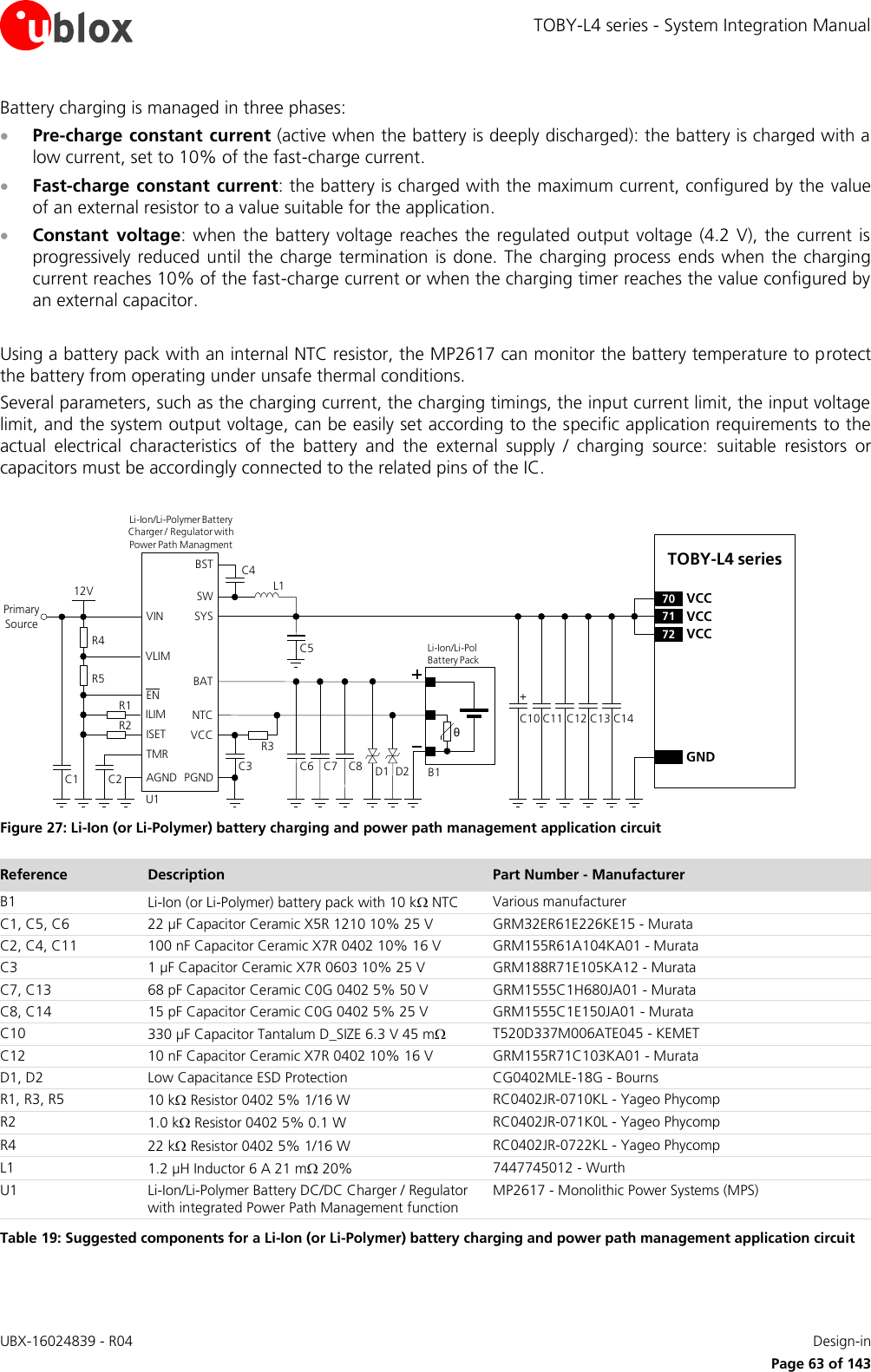
![TOBY-L4 series - System Integration Manual UBX-16024839 - R04 System description Page 31 of 143 1.6 System function interfaces 1.6.1 Module power-on TOBY-L4 series modules can be switched on in the following way: Low pulse on the PWR_ON pin, which is normally set high by an internal pull-up, for a valid time period, when the applied VCC voltage is stable at its nominal value within the valid operating range. As illustrated in Figure 12, the TOBY-L4 series PWR_ON input is equipped with an internal active pull-up resistor to an internal 1.3 V supply rail: the PWR_ON input voltage thresholds are different from the other generic digital interfaces, and the line should be driven by an open drain, by an open collector or by a contact switch, without an external pull-up resistor. Detailed electrical characteristics and specifications are described in TOBY-L4 series Data Sheet [1]. Baseband Processor20PWR_ONTOBY-L4 seriesPower-onPower ManagementPower-on35k1.3 V Figure 12: TOBY-L4 series PWR_ON input description TOBY-L4 series modules do not switch on by applying the VCC supply only: a low pulse must be forced on the PWR_ON pin when the VCC voltage is stable at its nominal value within the valid operating range.](https://usermanual.wiki/u-blox/1EHQ37NN.TempConfidential-TOBY-L4-SysIntegrManual-UBX-16024839/User-Guide-3759877-Page-31.png)
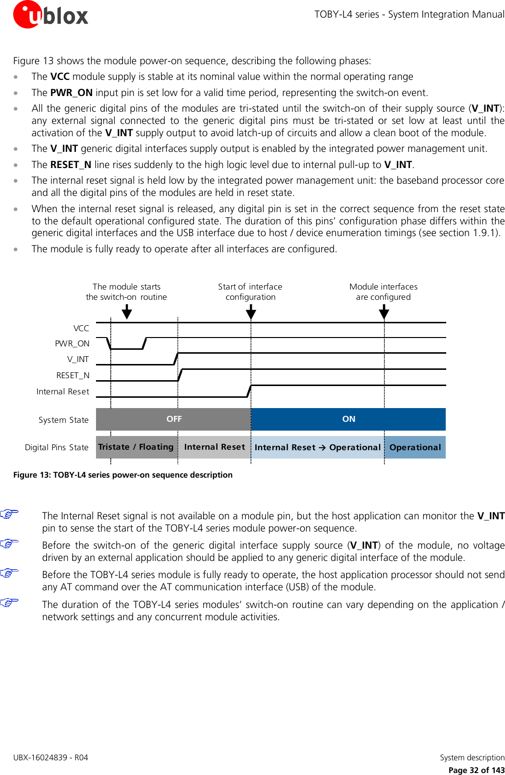
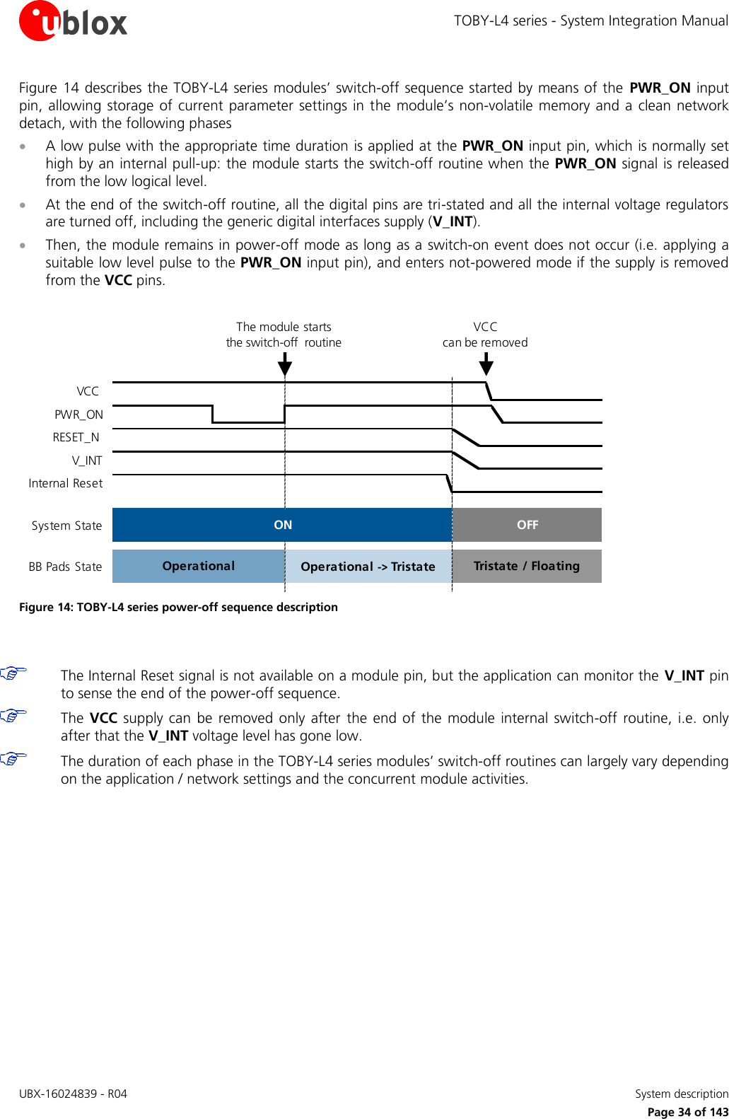
![TOBY-L4 series - System Integration Manual UBX-16024839 - R04 System description Page 33 of 143 1.6.2 Module power-off TOBY-L4 series can be properly switched off by: AT+CPWROFF command3 (see the u-blox AT Commands Manual [2]) uCPU application4 Low pulse on the PWR_ON pin, which is normally set high by an internal pull-up, for a valid time period (see the TOBY-L4 series Data Sheet [1]), module normal switch-off: the internal switch-off sequence of the module starts when the external application releases the PWR_ON line from the low logic level, after that it has been set low for an appropriate time period. The methods listed above represent the appropriate normal switch-off events, triggering an appropriate normal switch-off procedure of the module: the current parameter settings are saved in the module’s non-volatile memory and a clean network detach is performed. An abrupt under-voltage shutdown occurs on TOBY-L4 series modules when the VCC module supply is removed. If this occurs, it is not possible to perform the storing of the current parameter settings in the module’s non-volatile memory or to perform a clean network detach. It is highly recommended to avoid an abrupt removal of the VCC supply during TOBY-L4 series modules normal operations: the switch-off procedure must be started by an appropriate switch-off event (see above), and then a suitable VCC supply must be held at least until the end of the modules’ internal switch-off sequence, which occurs when the generic digital interfaces supply output (V_INT) is switched off by the module. An abrupt emergency shutdown procedure is triggered on TOBY-L4 series modules when a long enough low pulse is set at the PWR_ON input pin (see the TOBY-L4 series Data Sheet [1], module emergency switch-off). In this case, storage of the current parameter settings in the module’s non-volatile memory and the clean network detach are not performed. This abrupt emergency shutdown procedure is intended only for use for emergency, e.g. if the module does not provide a reply to a specific AT command after a time period longer than the one defined in the u-blox AT Commands Manual [2], or if shutdown via a normal switch-off procedure fails. An over-temperature shutdown occurs on TOBY-L4 series modules when the temperature measured within the cellular module reaches a critical range. 3 Not supported by "00" product version 4 Not supported by "50" product version](https://usermanual.wiki/u-blox/1EHQ37NN.TempConfidential-TOBY-L4-SysIntegrManual-UBX-16024839/User-Guide-3759877-Page-33.png)
![TOBY-L4 series - System Integration Manual UBX-16024839 - R04 System description Page 35 of 143 1.6.3 Module reset TOBY-L4 series modules can be properly reset (rebooted) by: AT+CFUN command5 (see the u-blox AT Commands Manual [2]) uCPU application6 The methods listed above represent appropriate reset (reboot) events, triggering an appropriate “internal” or “software” reset of the module: the current parameter settings are saved in the module’s non-volatile memory and a clean network detach is performed. An abrupt hardware reset occurs on TOBY-L4 series modules when a low level is applied on the RESET_N input pin. In this case, the current parameter settings are not saved in the module’s non-volatile memory and a clean network detach is not performed. It is highly recommended to avoid an abrupt hardware reset of the module by forcing a low level on the RESET_N input during modules normal operation: the RESET_N line should be set low only if reset via AT commands or if the uCPU application fails. As illustrated in Figure 15, the RESET_N input pins are equipped with an internal pull-up to the V_INT supply. Baseband Processor23RESET_NTOBY-L4 series5V_INTReset100k Figure 15: TOBY-L4 series RESET_N input equivalent circuit description 1.6.4 Module / host configuration selection Host Select pins are not supported by the "50" product version. TOBY-L4 series modules include two 1.8 V digital pins (HOST_SELECT0, HOST_SELECT1), which can be configured for External Interrupt detection or as GPIO by means of the uCPU API. 5 Not supported by "00" product version 6 Not supported by "50" product version](https://usermanual.wiki/u-blox/1EHQ37NN.TempConfidential-TOBY-L4-SysIntegrManual-UBX-16024839/User-Guide-3759877-Page-35.png)
![TOBY-L4 series - System Integration Manual UBX-16024839 - R04 System description Page 36 of 143 1.7 Antenna interfaces 1.7.1 Antenna RF interfaces (ANT1 / ANT2) TOBY-L4 series modules provide two RF interfaces for connecting the external antennas: The ANT1 represents the primary RF input/output for transmission and reception of LTE/3G/2G RF signals. The ANT1 pin has a nominal characteristic impedance of 50 and must be connected to the primary Tx / Rx antenna through a 50 transmission line to allow clean RF transmission and reception. The ANT2 represents the secondary RF input for the reception of the RF signals for CA, MIMO and Rx diversity configurations supported by TOBY-L4 series modules as a required feature for LTE category 6 UEs. The ANT2 pin has a nominal characteristic impedance of 50 and must be connected to the secondary Rx antenna through a 50 transmission line to allow for clean RF reception. 1.7.1.1 Antenna RF interfaces requirements Table 8, Table 9 and Table 10 summarize the requirements for the antennas’ RF interfaces (ANT1 / ANT2). See section 2.4.1 for suggestions on how to correctly design antennas circuits which are compliant with these requirements. The antenna circuits affect the RF compliance of the device integrating TOBY-L4 series modules with the applicable required certification schemes (for more details see section 4). Compliance is guaranteed if the antenna RF interfaces (ANT1 / ANT2) requirements summarized in Table 8, Table 9 and Table 10 are fulfilled. Item Requirements Remarks Impedance 50 nominal characteristic impedance The impedance of the antenna RF connection must match the 50 impedance of the ANT1 port. Frequency Range See the TOBY-L4 series Data Sheet [1] The required frequency range of the antenna connected to the ANT1 port depends on the operating bands of the used cellular module and the used mobile network. Return Loss S11 < -10 dB (VSWR < 2:1) recommended S11 < -6 dB (VSWR < 3:1) acceptable The Return loss or the S11, as the VSWR, refers to the amount of reflected power, measuring how well the antenna RF connection matches the 50 characteristic impedance of the ANT1 port. The impedance of the antenna termination must match as much as possible the 50 nominal impedance of the ANT1 port over the operating frequency range, reducing as much as possible the amount of reflected power. Efficiency > -1.5 dB ( > 70% ) recommended > -3.0 dB ( > 50% ) acceptable The radiation efficiency is the ratio of the radiated power to the power delivered to antenna input: the efficiency is a measure of how well an antenna receives or transmits. The radiation efficiency of the antenna connected to the ANT1 port needs to be enough high over the operating frequency range to comply with the Over-The-Air (OTA) radiated performance requirements, as Total Radiated Power (TRP) and the Total Isotropic Sensitivity (TIS), specified by applicable related certification schemes. Maximum Gain According to radiation exposure limits The power gain of an antenna is the radiation efficiency multiplied by the directivity: the gain describes how much power is transmitted in the direction of peak radiation to that of an isotropic source. The maximum gain of the antenna connected to ANT1 port must not exceed the herein stated value to comply with regulatory agencies’ radiation exposure limits. Input Power > 33 dBm ( > 2 W ) The antenna connected to the ANT1 port must support with adequate margin the maximum power transmitted by the modules. Table 8: Summary of primary Tx/Rx antenna RF interface (ANT1) requirements](https://usermanual.wiki/u-blox/1EHQ37NN.TempConfidential-TOBY-L4-SysIntegrManual-UBX-16024839/User-Guide-3759877-Page-36.png)
![TOBY-L4 series - System Integration Manual UBX-16024839 - R04 System description Page 37 of 143 Item Requirements Remarks Impedance 50 nominal characteristic impedance The impedance of the antenna RF connection must match the 50 impedance of the ANT2 port. Frequency Range See the TOBY-L4 series Data Sheet [1] The required frequency range of the antennas connected to ANT2 port depends on the operating bands of the used cellular module and the used mobile network. Return Loss S11 < -10 dB (VSWR < 2:1) recommended S11 < -6 dB (VSWR < 3:1) acceptable The Return loss or the S11, as the VSWR, refers to the amount of reflected power, measuring how well the antenna RF connection matches the 50 characteristic impedance of the ANT2 port. The impedance of the antenna termination must match as much as possible the 50 nominal impedance of the ANT2 port over the operating frequency range, reducing as much as possible the amount of reflected power. Efficiency > -1.5 dB ( > 70% ) recommended > -3.0 dB ( > 50% ) acceptable The radiation efficiency is the ratio of the radiated power to the power delivered to antenna input: the efficiency is a measure of how well an antenna receives or transmits. The radiation efficiency of the antenna connected to the ANT2 port needs to be enough high over the operating frequency range to comply with the Over-The-Air (OTA) radiated performance requirements, as the TIS, specified by applicable related certification schemes. Table 9: Summary of secondary Rx antenna RF interface (ANT2) requirements Item Requirements Remarks Efficiency imbalance < 0.5 dB recommended < 1.0 dB acceptable The radiation efficiency imbalance is the ratio of the primary (ANT1) antenna efficiency to the secondary (ANT2) antenna efficiency: the efficiency imbalance is a measure of how much better an antenna receives or transmits compared to the other antenna. The radiation efficiency of the secondary antenna needs to be roughly the same as the radiation efficiency of the primary antenna for good RF performance. Envelope Correlation Coefficient < 0.4 recommended < 0.5 acceptable The Envelope Correlation Coefficient (ECC) between the primary (ANT1) and the secondary (ANT2) antenna is an indicator of 3D radiation pattern similarity between the two antennas: low ECC results from antenna patterns with radiation lobes in different directions. The ECC between the primary and secondary antennas needs to be low enough to comply with the radiated performance requirements specified by related certification schemes. Isolation > 15 dB recommended > 10 dB acceptable The antenna to antenna isolation is the loss between the primary (ANT1) and the secondary (ANT2) antenna: high isolation results from low coupled antennas. The isolation between primary and secondary antenna needs to be high for good RF performance. Table 10: Summary of primary (ANT1) and secondary (ANT2) antennas relationship requirements](https://usermanual.wiki/u-blox/1EHQ37NN.TempConfidential-TOBY-L4-SysIntegrManual-UBX-16024839/User-Guide-3759877-Page-37.png)
![TOBY-L4 series - System Integration Manual UBX-16024839 - R04 System description Page 38 of 143 1.7.2 Antenna detection interface (ANT_DET) The antenna detection is based on ADC measurement. The ANT_DET pin is an Analog to Digital Converter (ADC) provided to sense the antenna presence. The antenna detection function provided by ANT_DET pin is an optional feature that can be implemented if the application requires it. The ANT_DET pin generates a DC current and measures the resulting DC voltage, thus determining the resistance from the antenna connector provided on the application board to GND. So the requirements to achieve antenna detection functionality are the following: an RF antenna assembly with a built-in resistor (diagnostic circuit) must be used an antenna detection circuit must be implemented on the application board See section 2.4.2 for the antenna detection circuit on the application board and the diagnostic circuit in the antenna assembly design-in guidelines. 1.8 SIM interfaces 1.8.1 SIM interfaces TOBY-L4 series modules provide two SIM interfaces for the direct connection of two external SIM cards/chips, which can be used alternatively (only one SIM at a time can be used for network access): SIM0 interface (VSIM, SIM_IO, SIM_CLK, SIM_RST pins), which is enabled by default SIM1 interface (VSIM1, SIM1_IO, SIM1_CLK, SIM1_RST pins), which can be alternatively enabled by dedicated AT command7 (see the u-blox AT Commands Manual [2]), or by means of the uCPU application8. Both 1.8 V and 3 V SIM types are supported by the SIM interfaces. Activation and deactivation with an automatic voltage switch from 1.8 V to 3 V is implemented according to ISO-IEC 7816-3 specifications. High-speed SIM/ME interface and the PPS procedure for baud-rate selection is implemented according to the values proposed by the SIM card/chip. Both the VSIM supply output and the VSIM1 supply output provide internal short circuit protection to limit the start-up current and protect the SIM from short circuits. 1.8.2 SIM detection interface The GPIO5 pin of TOBY-L4 series modules can be configured to detect the mechanical / physical presence of an external SIM card connected to the SIM0 interface. The pin can sense SIM card presence as intended to be properly connected to the mechanical switch of a SIM card holder as described in section 2.5: Low logic level at GPIO5 input pin is recognized as SIM card not present High logic level at GPIO5 input pin is recognized as SIM card present The SIM card detection function provided by GPIO5 pin is an optional feature that can be implemented / used or not according to the application requirements: an Unsolicited Result Code (URC) is generated each time that there is a change of status. The optional function “SIM card hot insertion/removal” can be additionally configured on the GPIO5 pin, in order to enable / disable the SIM0 interface upon detection of external SIM card physical insertion / removal. 7 Not supported by the "00" product version 8 Not supported by the "50" product version](https://usermanual.wiki/u-blox/1EHQ37NN.TempConfidential-TOBY-L4-SysIntegrManual-UBX-16024839/User-Guide-3759877-Page-38.png)
![TOBY-L4 series - System Integration Manual UBX-16024839 - R04 System description Page 40 of 143 1.9.1 USB interface The USB Super-Speed 3.0 compliant interface will be supported by future firmware versions. The USB High-Speed 2.0 host role is not supported by the "50" product versions. TOBY-L4 series modules include a USB Super-Speed 3.0 compliant interface, supporting up to 5 Gbit/s data rate, and also including a USB High-Speed 2.0 compliant interface, supporting up to 480 Mbit/s data rate. The USB High-Speed 2.0 compliant interface consists of the following pins: USB_D+/USB_D–, USB High-Speed differential transceiver data lines as per USB 2.0 specification [3] VUSB_DET input pin, which senses the VBUS USB supply presence (nominally 5 V at the source) to detect the host connection and enable the USB 2.0 interface with the module acting as a USB device. Neither the USB interface, nor the whole module is supplied by the VUSB_DET input pin, which senses the VBUS USB supply voltage presence and absorbs few microamperes. USB_ID pin, available for USB ID resistance measurement: if the USB_ID pin is externally connected to GND, then the module acts as a USB host if the USB_ID pin is externally left unconnected (floating), then the module acts as a USB device The USB High-Speed 2.0 compliant interface, with the module acting as a USB device, provides: AT command13 Data communication Ethernet-over-USB virtual channel Trace log capture (diagnostic purposes) Auxiliary channel to tune internal audio parameters using a dedicated external tool Linux console for uCPU applications development and debug14 FW upgrades The module, acting as a USB device, identifies itself by its VID (Vendor ID) and PID (Product ID) combination, included in the USB device descriptor according to the USB 2.0 specifications [3]. If the module, acting as a USB device, is connected to the USB host before the module is switched on, or if the module is reset (rebooted) with the USB connected to the host, the VID and PID are automatically updated during the boot of the module. First, the VID and PID are the following: VID = 0x8087 PID = 0x0801 This VID and PID combination identifies a USB profile where no USB function described above is available: the AT commands must not be sent to the module over the USB profile identified by this VID and PID combination. Then, after a time period (depending on the host / device enumeration timings), the VID and PID are updated to the one where the normal operative functions (AT, Data, Ethernet-over-USB, Trace, Linux console) are available. VID and PID for normal operative functions are the following: VID = 0x1546 PID = 0x1010 The USB High-Speed 2.0 compliant interface, with the module acting as USB host (OTG), provides: Communication with external device by means of the uCPU application 13 Not supported by the "00" product version 14 Not supported by the "50" product version](https://usermanual.wiki/u-blox/1EHQ37NN.TempConfidential-TOBY-L4-SysIntegrManual-UBX-16024839/User-Guide-3759877-Page-40.png)
![TOBY-L4 series - System Integration Manual UBX-16024839 - R04 System description Page 41 of 143 The USB Super-Speed 3.0 compliant interface as per USB 3.0 specifications [4], with the module acting as a USB device, consists of the following additional pins: USB_SSTX+/USB_SSTX–, USB Super-Speed differential transmitter data lines USB_SSRX+/USB_SSRX–, USB Super-Speed differential receiver data lines USB drivers are available for Windows operating system platforms. TOBY-L4 series modules are compatible with standard Linux/Android USB kernel drivers. 1.9.2 UART interfaces UART interfaces are not supported by the "50" product version, except for trace logging (diagnostic purposes) and Ring Indicator functionality over the UART0 interface. 1.9.2.1 UART0 interface The UART0 Universal Asynchronous Receiver/Transmitter serial interface has CMOS compatible signal levels (0 V for ON / active state and 1.8 V for OFF / idle state), providing: Communication with external devices by means of the uCPU API, over the following pins: o RXD module output and TXD module input data lines o CTS module output and RTS module input hardware flow control lines Trace logging (diagnostic purpose), over the following pins: o RXD module output and TXD module input data lines Ring Indicator functionality, over the following pin: o RI module output line The UART0 interface can operate at 9.6 kbit/s, 19.2 kbit/s, 38.4 kbit/s, 57.6 kbit/s, 115.2 kbit/s, 230.4 kbit/s, 460.8 kbit/s, 921.6 kbit/s, 3 Mbit/s, 3.25 Mbit/s and 6.5 Mbit/s baud rates, with 8N1 frame format (illustrated in Figure 16), and with hardware flow control output (CTS line) driven to the OFF state when the module is not prepared to accept data by the UART0 interface. D0 D1 D2 D3 D4 D5 D6 D7Start of 1-BytetransferStart Bit(Always 0)Possible Start ofnext transferStop Bit(Always 1)tbit = 1/(Baudrate)Normal Transfer, 8N1 Figure 16: Description of UART 8N1 frame format (8 data bits, no parity, 1 stop bit)](https://usermanual.wiki/u-blox/1EHQ37NN.TempConfidential-TOBY-L4-SysIntegrManual-UBX-16024839/User-Guide-3759877-Page-41.png)
![TOBY-L4 series - System Integration Manual UBX-16024839 - R04 System description Page 42 of 143 The RI line can notify an incoming call: the RI line is switched from the OFF state to the ON state with a 4:1 duty cycle and a 5 s period (ON for 1 s, OFF for 4 s, see Figure 17), until the DTE attached to the module sends the ATA string and the module accepts the incoming data call. The RING string sent by the module (DCE) to the serial port at constant time intervals is not correlated with the switch of the RI line to the ON state. Figure 17: RI behavior during an incoming call The RI output line can notify an SMS arrival. When the SMS arrives, the RI line switches from OFF to ON for 1 s (see Figure 18), if the feature is enabled by the AT+CNMI command (see the u-blox AT Commands Manual [2]). Figure 18: RI behavior at SMS arrival This behavior allows the DTE to stay in power saving mode until the DCE related event requests service. For SMS arrival, if several events coincidently occur or in quick succession, each event independently triggers the RI line, although the line will not be deactivated between each event. As a result, the RI line may stay to ON for more than 1 s, if an incoming call is answered within less than 1 s (with ATA or if auto-answering is set to ATS0=1) then the RI line is set to OFF earlier, so that: RI line monitoring cannot be used by the DTE to determine the number of received SMSs. For multiple events (incoming call plus SMS received), the RI line cannot be used to discriminate the two events, but the DTE must rely on subsequent URCs and interrogate the DCE with the suitable commands. The RI line can additionally notify URCs and/or incoming data, if the feature is enabled by the specific AT+URING command (for more details, see the u-blox AT Commands Manual [2]): the RI line is asserted when one of the configured events occur and it remains asserted for 1 s unless another configured event will happen, with the same behavior illustrated in Figure 18. The DTR, DSR, DCD and RI pins can be alternatively configured for External Interrupt detection or as GPIO by means of the uCPU API. The RI pin can be alternatively configured as GPIO by an AT command. SMS arrives time [s] 0 RI ON RI OFF 1s time [s] 0 RI ON RI OFF 1s 1stime [s]151050RI ONRI OFFCall incomes1stime [s]151050RI ONRI OFFCall incomes](https://usermanual.wiki/u-blox/1EHQ37NN.TempConfidential-TOBY-L4-SysIntegrManual-UBX-16024839/User-Guide-3759877-Page-42.png)
![TOBY-L4 series - System Integration Manual UBX-16024839 - R04 System description Page 45 of 143 1.9.4 DDC (I2C) interfaces DDC (I2C) interfaces are not supported by the "50" product version. 1.9.4.1 I2C0 interface The SDA and SCL pins represent the I2C0 1.8 V I2C bus compatible Display Data Channel (DDC) interface, with the module acting as I2C master, available for communication with u-blox GNSS chips / modules communication with other external I2C devices by means of the uCPU API The I2C0 interface pins of the module are open drain outputs conforming to the I2C bus specifications [6], supporting up to 100 kbit/s data rate in Standard mode, and up to 400 kbit/s data rate in Fast mode. External pull-up resistors to suitable 1.8 V supply (e.g. V_INT) are required for operations. u-blox has implemented special features to ease the design effort required for the integration of a u-blox cellular module with a u-blox GNSS receiver. Combining a u-blox cellular module with a u-blox GNSS receiver allows designers to have full access to the positioning receiver directly via the cellular module: it relays control messages to the GNSS receiver via a dedicated DDC (I2C) interface. An interface connected to the positioning receiver is not necessary: the cellular module allows full control of the GNSS receiver. The modules provide embedded GNSS aiding that is a set of specific features developed by u-blox to improve the cellular / GNSS system power consumption and the GNSS performance, decreasing the Time-To-First-Fix (TTFF), thus allowing to calculate the position in a shorter time with higher accuracy. 1.9.4.2 I2C1 interface The SDA and SCL pins represent the I2C1 I2C bus compatible Display Data Channel (DDC) interface, with the module acting as the I2C master, available for communication with other external I2C devices by means of uCPU API The I2C1 interface pins of the module are open drain outputs conforming to the I2C bus specifications [6], supporting up to 100 kbit/s data rate in Standard mode, and up to 400 kbit/s data rate in Fast mode. External pull-up resistors to a suitable 1.8 V supply (e.g. V_INT) are required for operations. 1.9.5 SDIO interface SDIO interface is not supported by the "50" product version. TOBY-L4 series modules include a 4-bit Secure Digital Input Output interface (SDIO_D0, SDIO_D1, SDIO_D2, SDIO_D3, SDIO_CLK, SDIO_CMD), where the module acts as an SDIO host controller designed to communicate with compatible u-blox short range radio communication modules by means of the uCPU API communicate with external SDIO devices by means of the uCPU API The SDIO interface supports up to 832 Mbit/s data rate with SD 3.0 SDR104 mode at 208 MHz clock frequency. Combining a u-blox cellular module with a u-blox short range communication module gives designers full access to the Wi-Fi module directly via the cellular module, so that a second interface connected to the Wi-Fi module is not necessary. The cellular module allows a full control of the Wi-Fi module, because Wi-Fi control messages are relayed to the Wi-Fi module via the dedicated SDIO interface. u-blox has implemented special features in the cellular modules to ease the design effort for the integration of a u-blox cellular module with a u-blox short range Wi-Fi module to provide Router functionality.](https://usermanual.wiki/u-blox/1EHQ37NN.TempConfidential-TOBY-L4-SysIntegrManual-UBX-16024839/User-Guide-3759877-Page-45.png)
![TOBY-L4 series - System Integration Manual UBX-16024839 - R04 System description Page 46 of 143 1.9.6 RGMII interface RGMII interface is not supported by the "50" product version. TOBY-L4 series modules include an Ethernet Media Access Control (MAC) block supporting up to 1 Gbit/s data rate via a Reduced Gigabit Media-Independent Interface compliant with the RGMII Version 1.3 specification [7] and the RMII Revision 1.2 specification [8]. The module represents an Ethernet MAC controller, which can be connected to an external Ethernet physical transceiver (PHY) chip for communication with a remote processor over Ethernet. The following signals are provided for communication and management of an external Ethernet PHY: V_ETH Interface supply output ETH_TX_CLK RGMII Transmit reference Clock (TXC) output RMII Reference Clock (REF_CLK) output ETH_TX_CTL RGMII Transmit Control output, driven on both edges of the Transmit clock (TXC) RMII Transmit Enable (TXEN) output, synchronous with Reference Clock (REF_CLK) ETH_TXD0 RGMII / RMII Transmit Data [0], from MAC to PHY (module output) ETH_TXD1 RGMII / RMII Transmit Data [1], from MAC to PHY (module output) ETH_TXD2 RGMII Transmit Data [2], from MAC to PHY (module output) ETH_TXD3 RGMII Transmit Data [3], from MAC to PHY (module output) ETH_RX_CLK RGMII Receive reference Clock (RXC) input ETH_RX_CTL RGMII Receive Control input, sampled on both edges of the Receive clock (RXC) RMII Carrier Sense (CRS) / Receive Data Valid (RX_DV) input ETH_RXD0 RGMII / RMII Receive Data [0], from PHY to MAC (module input) ETH_RXD1 RGMII / RMII Receive Data [1], from PHY to MAC (module input) ETH_RXD2 RGMII Receive Data [2], from PHY to MAC (module input) ETH_RXD3 RGMII Receive Data [3], from PHY to MAC (module input) ETH_INTR Ethernet Interrupt Input, from PHY to MAC (module input) When this signal is high, it indicates an interrupt event in the PHY ETH_MDIO Management Data Input Output, bidirectional signal (module input/output) ETH_MDC Management Data Clock, from MAC to PHY (module output)](https://usermanual.wiki/u-blox/1EHQ37NN.TempConfidential-TOBY-L4-SysIntegrManual-UBX-16024839/User-Guide-3759877-Page-46.png)
![TOBY-L4 series - System Integration Manual UBX-16024839 - R04 System description Page 47 of 143 1.10 eMMC interface The eMMC interface is not supported by the "50" product version. TOBY-L4 series modules include a 4-bit embedded Multi-Media Card interface compliant with the JESD84-B451 Embedded Multimedia Card (eMMC) Electrical Standard 4.51 [9]. The following signals are provided for connection and management of an external eMMC / SD memory by means of the uCPU API: V_MMC Interface supply output (module output) MMC_D0 Multi-Media Card Data [0], bidirectional signal (module input/output) MMC_D1 Multi-Media Card Data [1], bidirectional signal (module input/output) MMC_D2 Multi-Media Card Data [2], bidirectional signal (module input/output) MMC_D3 Multi-Media Card Data [3], bidirectional signal (module input/output) MMC_CMD Multi-Media Card Command, bidirectional signal (module input/output) MMC_CLK Multi-Media Card Clock (module output) MMC_RST_N Multi-Media Card Reset (module output) MMC_CD_N Multi-Media Card Detect (module input)](https://usermanual.wiki/u-blox/1EHQ37NN.TempConfidential-TOBY-L4-SysIntegrManual-UBX-16024839/User-Guide-3759877-Page-47.png)
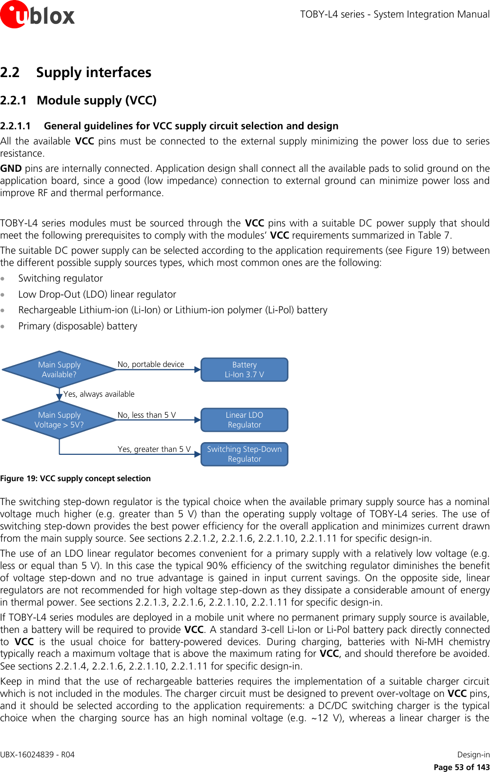
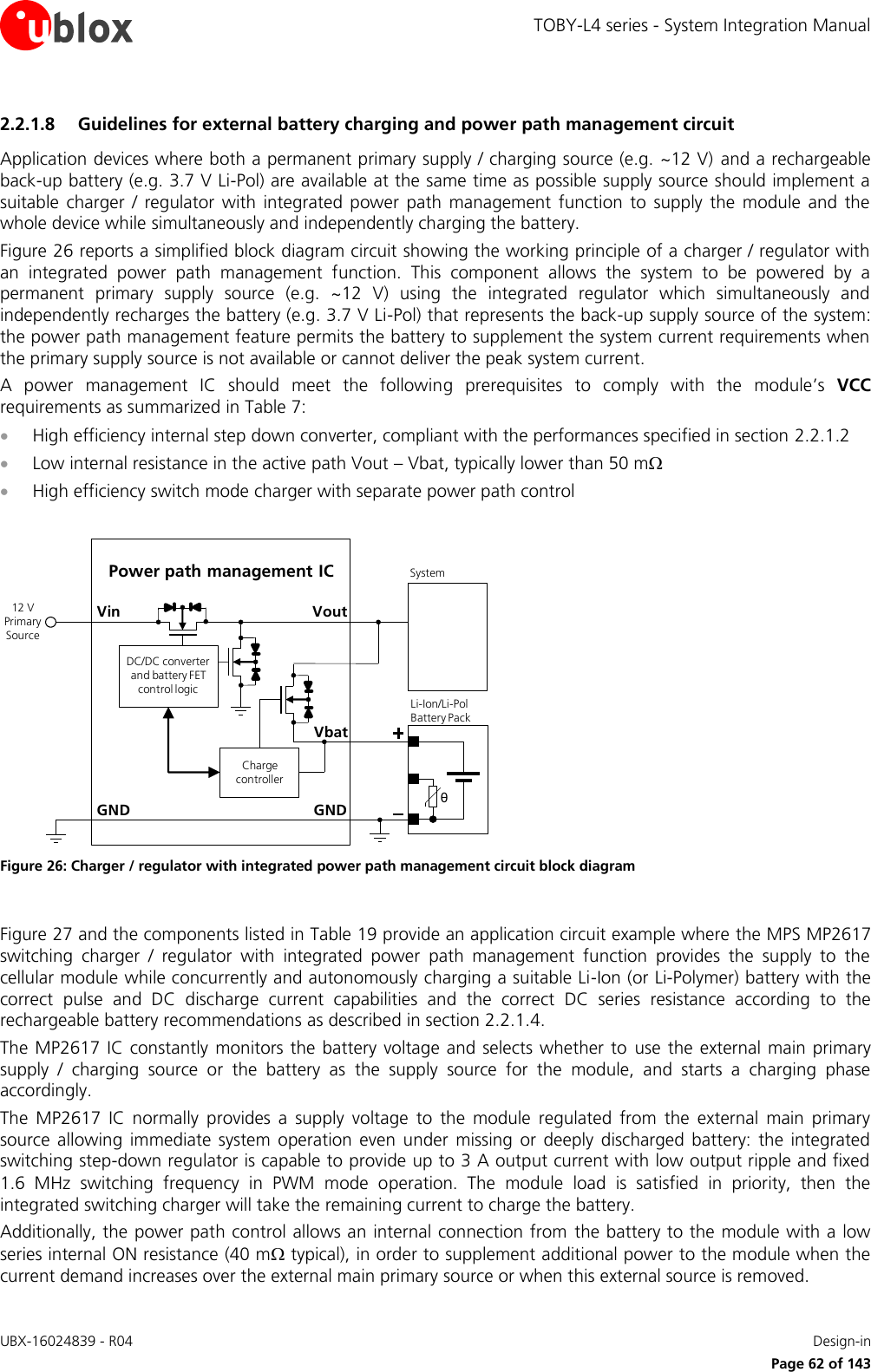
![TOBY-L4 series - System Integration Manual UBX-16024839 - R04 Design-in Page 54 of 143 typical choice when the charging source has a relatively low nominal voltage (~5 V). If both a permanent primary supply / charging source (e.g. ~12 V) and a rechargeable back-up battery (e.g. 3.7 V Li-Pol) are available at the same time as possible supply source, then a suitable charger / regulator with integrated power path management function can be selected to supply the module while simultaneously and independently charging the battery. See sections 2.2.1.7, 2.2.1.8, and 2.2.1.4, 2.2.1.6, 2.2.1.10, 2.2.1.11 for specific design-in. An appropriate primary (not rechargeable) battery can be selected taking into account the maximum current specified in the TOBY-L4 series Data Sheet [1] during connected mode, considering that primary cells might have weak power capability. See sections 2.2.1.5, and 2.2.1.6, 2.2.1.10, 2.2.1.11 for specific design-in. The usage of more than one DC supply at the same time should be evaluated carefully: depending on the supply source characteristics, different DC supply systems can result as mutually exclusive. The usage of a regulator or a battery not able to support the highest peak of VCC current consumption specified in the TOBY-L4 series Data Sheet [1] is generally not recommended. However, if the selected regulator or battery is not able to support the highest peak current of the module, it must be able to support with adequate margin at least the highest averaged current consumption value specified in the TOBY-L4 series Data Sheet [1]. The additional energy required by the module during a 2G Tx slot can be provided by an appropriate bypass tank capacitor or a super-capacitor with very large capacitance and very low ESR placed close to the module VCC pins. Depending on the actual capability of the selected regulator or battery, the required capacitance can be considerably larger than 1 mF and the required ESR can be in the range of few tens of m. Carefully evaluate the super-capacitor characteristics since aging and temperature may affect the actual characteristics. The following sections highlight some design aspects for each of the supplies listed above providing application circuit design-in compliant with the module VCC requirements summarized in Table 7. 2.2.1.2 Guidelines for VCC supply circuit design using a switching regulator The use of a switching regulator is suggested when the difference from the available supply rail source to the VCC value is high, since switching regulators provide good efficiency transforming a 12 V or greater voltage supply to the typical 3.8 V value of the VCC supply. The characteristics of the switching regulator connected to VCC pins should meet the following prerequisites to comply with the module VCC requirements summarized in Table 7: Power capability: the switching regulator with its output circuit must be capable of providing a voltage value to the VCC pins within the specified operating range and must be capable of delivering to VCC pins the maximum peak / pulse current consumption during Tx burst at maximum Tx power specified in the TOBY-L4 series Data Sheet [1]. Low output ripple: the switching regulator together with its output circuit must be capable of providing a clean (low noise) VCC voltage profile. High switching frequency: for best performance and for smaller applications it is recommended to select a switching frequency ≥ 600 kHz (since L-C output filter is typically smaller for high switching frequency). The use of a switching regulator with a variable switching frequency or with a switching frequency lower than 600 kHz must be evaluated carefully since this can produce noise in the VCC voltage profile and therefore negatively impact LTE/3G/2G modulation spectrum performance. An additional L-C low-pass filter between the switching regulator output to VCC supply pins can mitigate the ripple at the input of the module, but adds extra voltage drop due to resistive losses on series inductors. PWM mode operation: it is preferable to select regulators with Pulse Width Modulation (PWM) mode. While in connected mode, the Pulse Frequency Modulation (PFM) mode and PFM/PWM modes transitions must be avoided to reduce noise on VCC voltage profile. Switching regulators can be used that are able to switch between low ripple PWM mode and high ripple PFM mode, provided that the mode transition occurs when the module changes status from the idle/active modes to connected mode. It is permissible to use a regulator that switches from the PWM mode to the burst or PFM mode at an appropriate current threshold.](https://usermanual.wiki/u-blox/1EHQ37NN.TempConfidential-TOBY-L4-SysIntegrManual-UBX-16024839/User-Guide-3759877-Page-54.png)
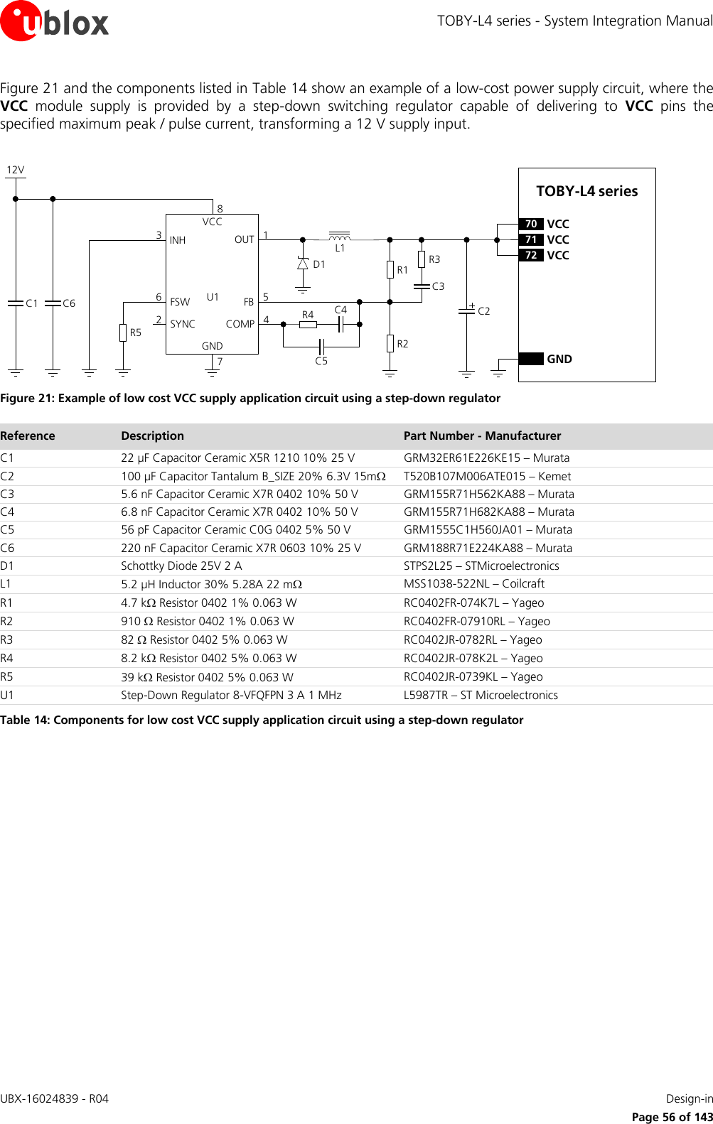
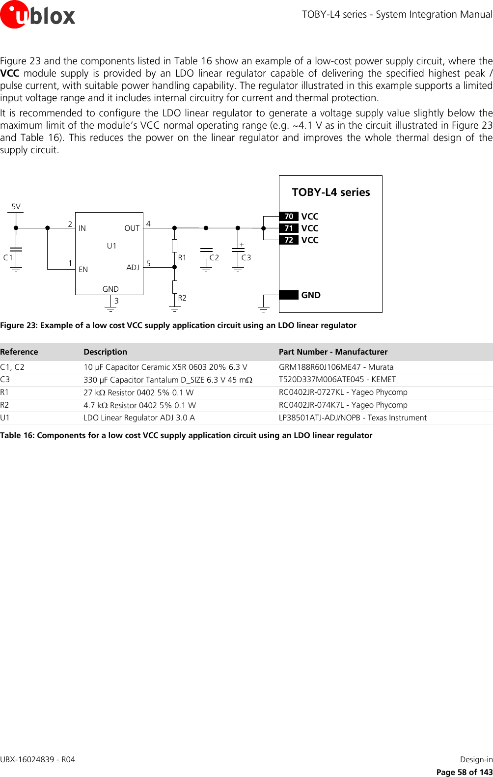
![TOBY-L4 series - System Integration Manual UBX-16024839 - R04 Design-in Page 57 of 143 2.2.1.3 Guidelines for VCC supply circuit design using a Low Drop-Out linear regulator The use of a linear regulator is suggested when the difference from the available supply rail source and the VCC value is low. The linear regulators provide high efficiency when transforming a 5 VDC supply to a voltage value within the module VCC normal operating range. The characteristics of the Low Drop-Out (LDO) linear regulator connected to the VCC pins should meet the following prerequisites to comply with the module VCC requirements summarized in Table 7: Power capabilities: the LDO linear regulator with its output circuit must be capable of providing a voltage value to the VCC pins within the specified operating range and must be capable of delivering to the VCC pins the maximum peak / pulse current consumption during Tx burst at maximum Tx power specified in the TOBY-L4 series Data Sheet [1]. Power dissipation: the power handling capability of the LDO linear regulator must be checked to limit its junction temperature to the maximum rated operating range (i.e. check the voltage drop from the maximum input voltage to the minimum output voltage to evaluate the power dissipation of the regulator). Figure 22 and the components listed in Table 15 show an example of a power supply circuit where the VCC module supply is provided by an LDO linear regulator capable of delivering the required current with a suitable power handling capability. It is recommended to configure the LDO linear regulator to generate a voltage supply value slightly below the maximum limit of the module VCC normal operating range (e.g. ~4.1 V for the VCC, as in the circuits illustrated in Figure 22 and Table 15). This reduces the power on the linear regulator and improves the thermal design of the circuit. 5VC1 R1IN OUTADJGND12453C2R2R3U1SHDNTOBY-L4 series71 VCC72 VCC70 VCCGNDC3 Figure 22: Example of high reliability VCC supply application circuit using an LDO linear regulator Reference Description Part Number - Manufacturer C1, C2 10 µF Capacitor Ceramic X5R 0603 20% 6.3 V GRM188R60J106ME47 - Murata C3 330 µF Capacitor Tantalum D_SIZE 6.3 V 45 m T520D337M006ATE045 - KEMET R1 47 k Resistor 0402 5% 0.1 W RC0402JR-0747KL - Yageo Phycomp R2 9.1 k Resistor 0402 5% 0.1 W RC0402JR-079K1L - Yageo Phycomp R3 3.9 k Resistor 0402 5% 0.1 W RC0402JR-073K9L - Yageo Phycomp U1 LDO Linear Regulator ADJ 3.0 A LT1764AEQ#PBF - Linear Technology Table 15: Components for high reliability VCC supply application circuit using an LDO linear regulator](https://usermanual.wiki/u-blox/1EHQ37NN.TempConfidential-TOBY-L4-SysIntegrManual-UBX-16024839/User-Guide-3759877-Page-57.png)
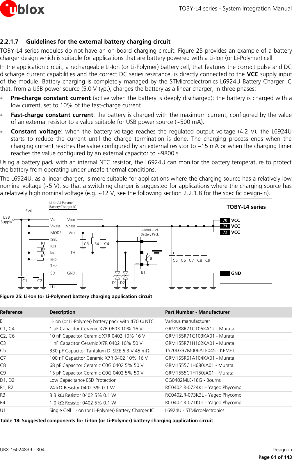
![TOBY-L4 series - System Integration Manual UBX-16024839 - R04 Design-in Page 59 of 143 2.2.1.4 Guidelines for VCC supply circuit design using a rechargeable Li-Ion or Li-Pol battery Rechargeable Li-Ion or Li-Pol batteries connected to the VCC pins should meet the following prerequisites to comply with the module’s VCC requirements as summarized in Table 7: Maximum pulse and DC discharge current: the rechargeable Li-Ion battery with its related output circuit connected to the VCC pins must be capable of delivering a pulse current as the maximum peak / pulse current consumption during Tx burst at the maximum Tx power specified in the TOBY-L4 series Data Sheet [1] and must be capable of extensively delivering a DC current as the maximum average current consumption as specified in the TOBY-L4 series Data Sheet [1]. The maximum discharge current is not always reported in the data sheets of batteries, but the maximum DC discharge current is typically almost equal to the battery capacity in Amp-hours divided by 1 hour. DC series resistance: the rechargeable Li-Ion battery with its output circuit must be capable of avoiding a VCC voltage drop below the operating range summarized in Table 7 during transmit bursts. 2.2.1.5 Guidelines for VCC supply circuit design using a primary (disposable) battery The characteristics of a primary (non-rechargeable) battery connected to the VCC pins should meet the following prerequisites to comply with the module’s VCC requirements as summarized in Table 7: Maximum pulse and DC discharge current: the non-rechargeable battery with its related output circuit connected to the VCC pins must be capable of delivering a pulse current as the maximum peak current consumption during Tx burst at the maximum Tx power specified in the TOBY-L4 series Data Sheet [1] and must be capable of extensively delivering a DC current as the maximum average current consumption as specified in the TOBY-L4 series Data Sheet [1]. The maximum discharge current is not always reported in the data sheets of batteries, but the maximum DC discharge current is typically almost equal to the battery capacity in Amp-hours divided by 1 hour. DC series resistance: the non-rechargeable battery with its output circuit must be capable of avoiding a VCC voltage drop below the operating range as summarized in Table 7 during transmit bursts.](https://usermanual.wiki/u-blox/1EHQ37NN.TempConfidential-TOBY-L4-SysIntegrManual-UBX-16024839/User-Guide-3759877-Page-59.png)
![TOBY-L4 series - System Integration Manual UBX-16024839 - R04 Design-in Page 60 of 143 2.2.1.6 Additional guidelines for VCC supply circuit design To reduce voltage drops, use a low impedance power source. The series resistance of the power supply lines (connected to the modules’ VCC and GND pins) on the application board and battery pack should also be considered and minimized: cabling and routing must be as short as possible to minimize power losses. Three pins are allocated to the VCC supply. Several pins are designated for GND connection. It is recommended to correctly connect all of them to supply the module to minimize series resistance losses. For modules supporting 2G radio access technology, to avoid voltage drop undershoot and overshoot at the start and end of a transmit burst during a GSM call (when current consumption on the VCC supply can rise up as specified in the TOBY-L4 series Data Sheet [1]), place a bypass capacitor with large capacitance (at least 100 µF) and low ESR near the VCC pins, for example: 330 µF capacitance, 45 m ESR (e.g. KEMET T520D337M006ATE045, Tantalum Capacitor) To reduce voltage ripple and noise, improving RF performance especially if the application device integrates an internal antenna, place the following bypass capacitors near the VCC pins: 68 pF capacitor with Self-Resonant Frequency in the 800/900 MHz range (e.g. Murata GRM1555C1H680J) 15 pF capacitor with Self-Resonant Frequency in 1800/1900 MHz range (e.g. Murata GRM1555C1E150J) 8.2 pF capacitor with Self-Resonant Frequency in 2500/2600 MHz range (e.g. Murata GRM1555C1H8R2D) 10 nF capacitor (e.g. Murata GRM155R71C103K) to filter digital logic noise from clocks and data sources 100 nF capacitor (e.g. Murata GRM155R61C104K) to filter digital logic noise from clocks and data sources A suitable series ferrite bead can be correctly placed on the VCC line for additional noise filtering if required by the specific application according to the whole application board design. C2GNDC3 C4TOBY-L4 series71VCC72VCC70VCCC1 C5 C63V8+ Figure 24: Suggested schematic for the VCC bypass capacitors to reduce ripple / noise on the supply voltage profile Reference Description Part Number - Manufacturer C1 8.2 pF Capacitor Ceramic C0G 0402 5% 50 V GRM1555C1H8R2DZ01 - Murata C2 15 pF Capacitor Ceramic C0G 0402 5% 50 V GRM1555C1H150JA01 - Murata C3 68 pF Capacitor Ceramic C0G 0402 5% 50 V GRM1555C1H680JA01 - Murata C4 10 nF Capacitor Ceramic X7R 0402 10% 16 V GRM155R71C103KA01 - Murata C5 100 nF Capacitor Ceramic X7R 0402 10% 16 V GRM155R71C104KA01 - Murata C6 330 µF Capacitor Tantalum D_SIZE 6.3 V 45 m T520D337M006ATE045 - KEMET Table 17: Suggested components to reduce ripple / noise on the VCC The necessity of each part depends on the specific design, but it is recommended to provide all the bypass capacitors illustrated in Figure 24 / Table 17 if the application device integrates an internal antenna. The ESD sensitivity rating of the VCC supply pins is 1 kV (HBM as per JESD22-A114). A higher protection level can be required if the line is externally accessible on the application board, e.g. if the accessible battery connector is directly connected to the supply pins. A higher protection level can be achieved by mounting an ESD protection (e.g. EPCOS CA05P4S14THSG varistor) close to the accessible point.](https://usermanual.wiki/u-blox/1EHQ37NN.TempConfidential-TOBY-L4-SysIntegrManual-UBX-16024839/User-Guide-3759877-Page-60.png)
![TOBY-L4 series - System Integration Manual UBX-16024839 - R04 Design-in Page 64 of 143 2.2.1.9 Guidelines for removing VCC supply As described in section 1.6.2 and Figure 14, the VCC supply can be removed after the end of the TOBY-L4 series module’s internal power-off sequence, which must be properly started as described in section 1.6.2. Removing the VCC power can be useful in order to minimize the current consumption when the TOBY-L4 series modules are switched off. Then, the modules can be switched on again by re-applying the VCC supply. If the VCC supply is generated by a switching or an LDO regulator, the application processor may control the input pin of the regulator which is provided to enable / disable the output of the regulator (as for example, the RUN input pin for the regulator illustrated in Figure 20, the INH input pin for the regulator illustrated in Figure 21, the SHDNn input pin for the regulator illustrated in Figure 22, or the EN input pin for the regulator illustrated in Figure 23), in order to apply / remove the VCC supply. If the regulator that generates the VCC supply does not provide an on / off pin, or for other applications such as the battery-powered ones, the VCC supply can be switched off using an appropriate external p-channel MOSFET controlled by the application processor by means of a suitable inverting transistor as shown in Figure 28, given that the external p-channel MOSFET has provided: Very low RDS(ON) (for example, less than 50 m), to minimize voltage drops Adequate maximum Drain current (see the TOBY-L4 series Data Sheet [1] for module consumption figures) Low leakage current, to minimize the current consumption C3GNDC2C1 C4TOBY-L4 series71 VCC72 VCC70 VCC+VCC Supply SourceGNDGPIO C5R1R3R2T2T1Application Processor Figure 28: Example of application circuit for VCC supply removal Reference Description Part Number - Manufacturer R1 47 k Resistor 0402 5% 0.1 W RC0402JR-0747KL - Yageo Phycomp R2 10 k Resistor 0402 5% 0.1 W RC0402JR-0710KL - Yageo Phycomp R3 100 k Resistor 0402 5% 0.1 W RC0402JR-07100KL - Yageo Phycomp T1 P-Channel MOSFET Low On-Resistance AO3415 - Alpha & Omega Semiconductor Inc. T2 NPN BJT Transistor BC847 - Infineon C1 330 µF Capacitor Tantalum D_SIZE 6.3 V 45 m T520D337M006ATE045 - KEMET C2 10 nF Capacitor Ceramic X7R 0402 10% 16 V GRM155R71C103KA01 - Murata C3 100 nF Capacitor Ceramic X7R 0402 10% 16 V GRM155R61A104KA01 - Murata C4 56 pF Capacitor Ceramic C0G 0402 5% 25 V GRM1555C1E560JA01 - Murata C5 15 pF Capacitor Ceramic C0G 0402 5% 25 V GRM1555C1E150JA01 - Murata Table 20: Components for VCC supply removal application circuit It is highly recommended to avoid an abrupt removal of the VCC supply during the TOBY-L4 series module’s normal operations: the power off procedure must be started as described in section 1.6.2, and then a suitable VCC supply must be held at least until the end of the modules’ internal power off sequence, which occurs when the generic digital interfaces supply output (V_INT) is switched off by the module.](https://usermanual.wiki/u-blox/1EHQ37NN.TempConfidential-TOBY-L4-SysIntegrManual-UBX-16024839/User-Guide-3759877-Page-64.png)
![TOBY-L4 series - System Integration Manual UBX-16024839 - R04 Design-in Page 66 of 143 2.2.2 RTC back-up supply (V_BCKP) 2.2.2.1 Guidelines for V_BCKP circuit design TOBY-L4 series modules provide the V_BCKP pin, which can be used to: power the Real Time Clock (RTC) only when the voltage value at VCC main module supply input is too low The RTC can be supplied from an external back-up battery or capacitor through the V_BCKP pin, when the main module voltage supply is not applied to the VCC pins. This lets the time reference (date and time) run as long as the V_BCKP voltage is within its valid range, even when the main supply is not provided to the module. Figure 29 and Table 21 describe possible application circuits for V_BCKP Real Time Clock (RTC) back-up supply: a. 100 µF capacitor, to let the RTC run for ~1 minute after the VCC removal b. 70 mF super-capacitor with a 4.7 k series resistor, to let the RTC run for ~1 hour after the VCC removal c. Coin non-rechargeable battery with series diode, to let the RTC run for days after the VCC removal TOBY-L4 seriesC1a.3V_BCKPR2TOBY-L4 seriesC2(SuperCap)b.3V_BCKPD3TOBY-L4 seriesB3c.3V_BCKP Figure 29: RTC back-up supply (V_BCKP) application circuits using a capacitor, a super-capacitor, or a non-rechargeable battery Reference Description Part Number - Manufacturer C1 100 µF Tantalum Capacitor GRM43SR60J107M - Murata R2 4.7 k Resistor 0402 5% 0.1 W RC0402JR-074K7L - Yageo Phycomp C2 70 mF Capacitor XH414H-IV01E - Seiko Instruments Table 21: Example of components for RTC back-up supply (V_BCKP) The V_BCKP supply output pin provides internal short circuit protection to limit the start-up current and protect the device in short circuit situations. No additional external short circuit protection is required. The V_BCKP pin can be left unconnected if the RTC timing is not required when the VCC supply is removed. The internal regulator for V_BCKP is optimized for low leakage current and very light loads. Do not apply loads which might exceed the limit for the maximum available current from V_BCKP supply, as this can cause malfunctions in the module. The TOBY-L4 series Data Sheet [1] describes the detailed electrical characteristics. The ESD sensitivity rating of the V_BCKP supply pin is 1 kV (HBM according to JESD22-A114). A higher protection level can be required if the line is externally accessible on the application board, e.g. if an accessible back-up battery connector is directly connected to the V_BCKP pin, and it can be achieved by mounting an ESD protection (e.g. EPCOS CA05P4S14THSG varistor array) close to the accessible point. 2.2.2.2 Guidelines for V_BCKP layout design The V_BCKP supply requires careful layout: avoid injecting noise on this voltage domain, as it may affect the stability of the internal circuitry.](https://usermanual.wiki/u-blox/1EHQ37NN.TempConfidential-TOBY-L4-SysIntegrManual-UBX-16024839/User-Guide-3759877-Page-66.png)
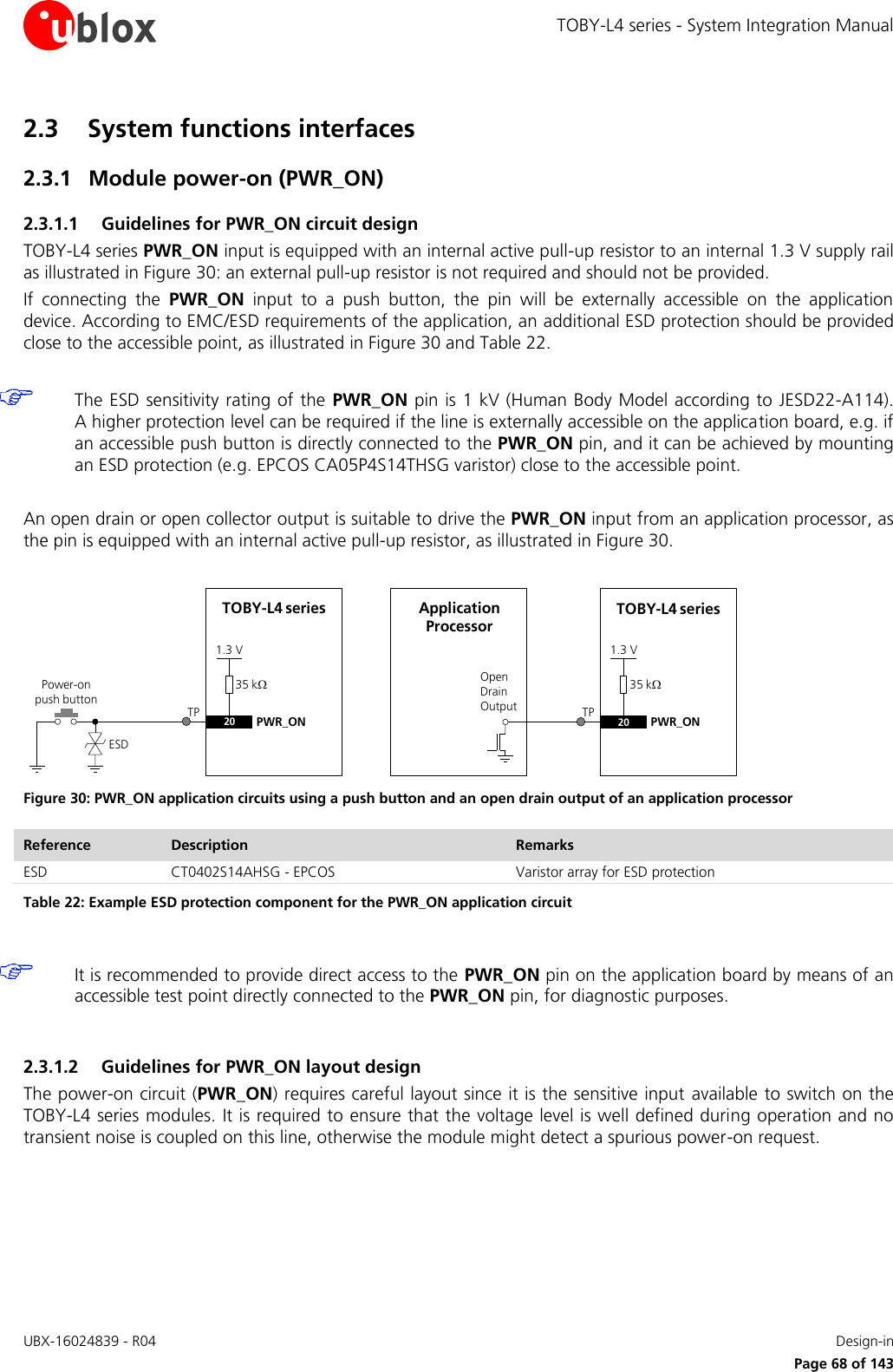
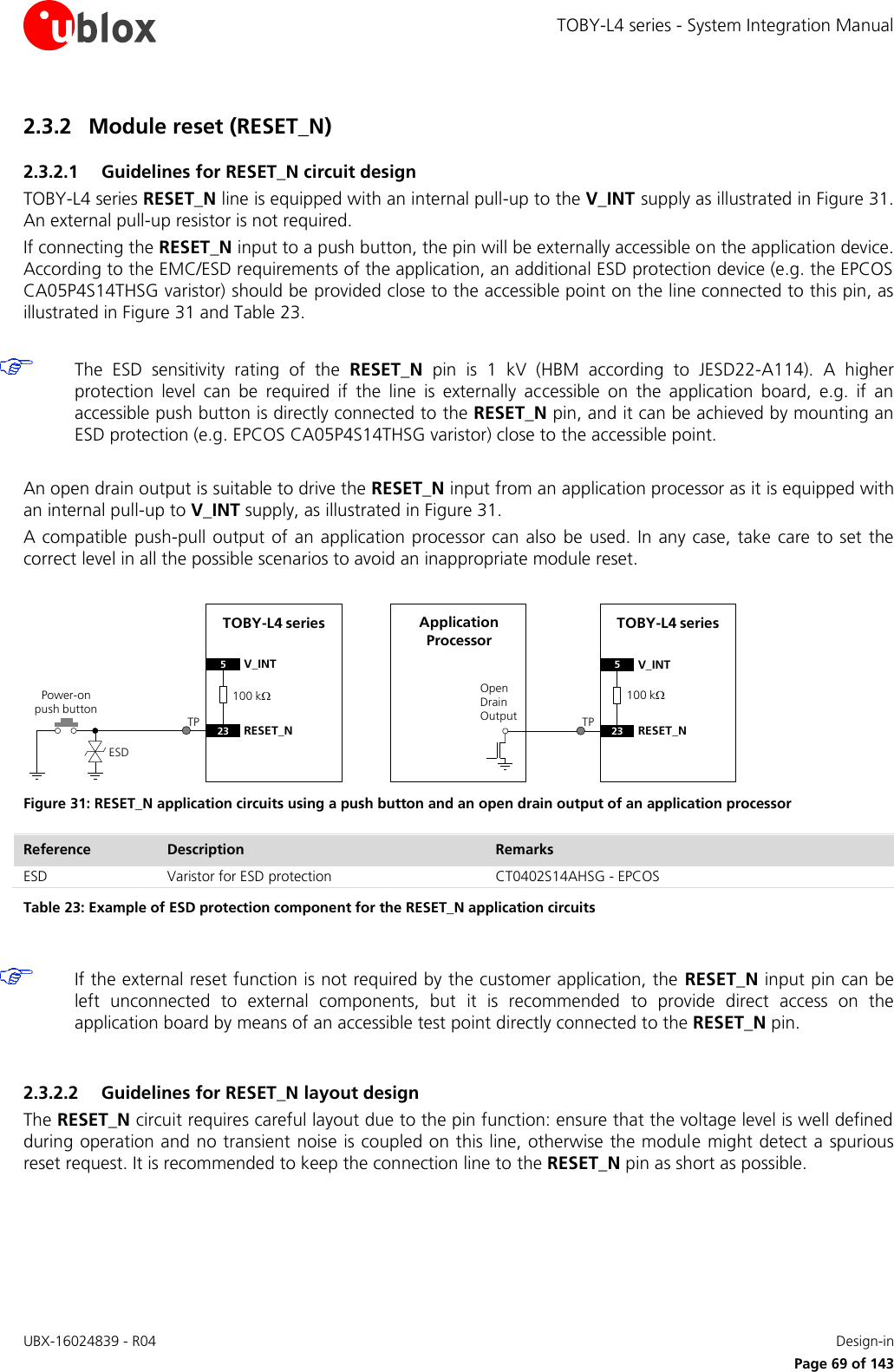
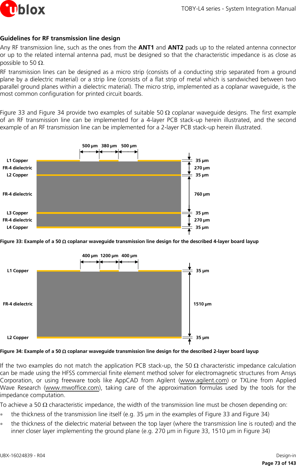
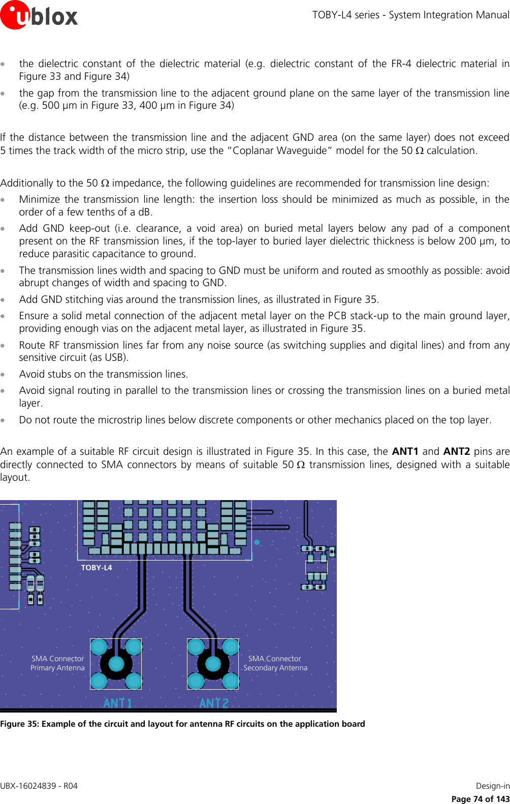
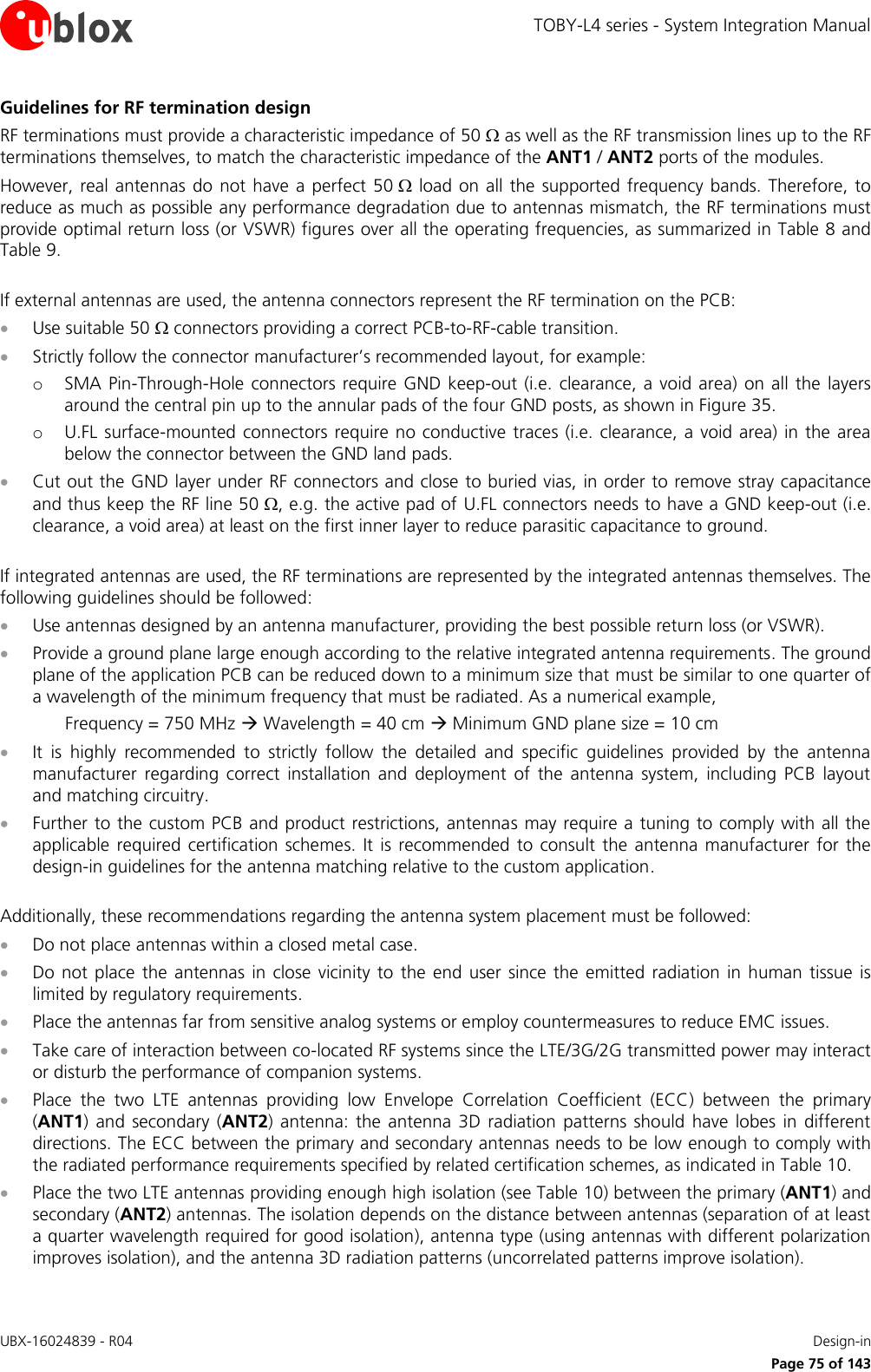
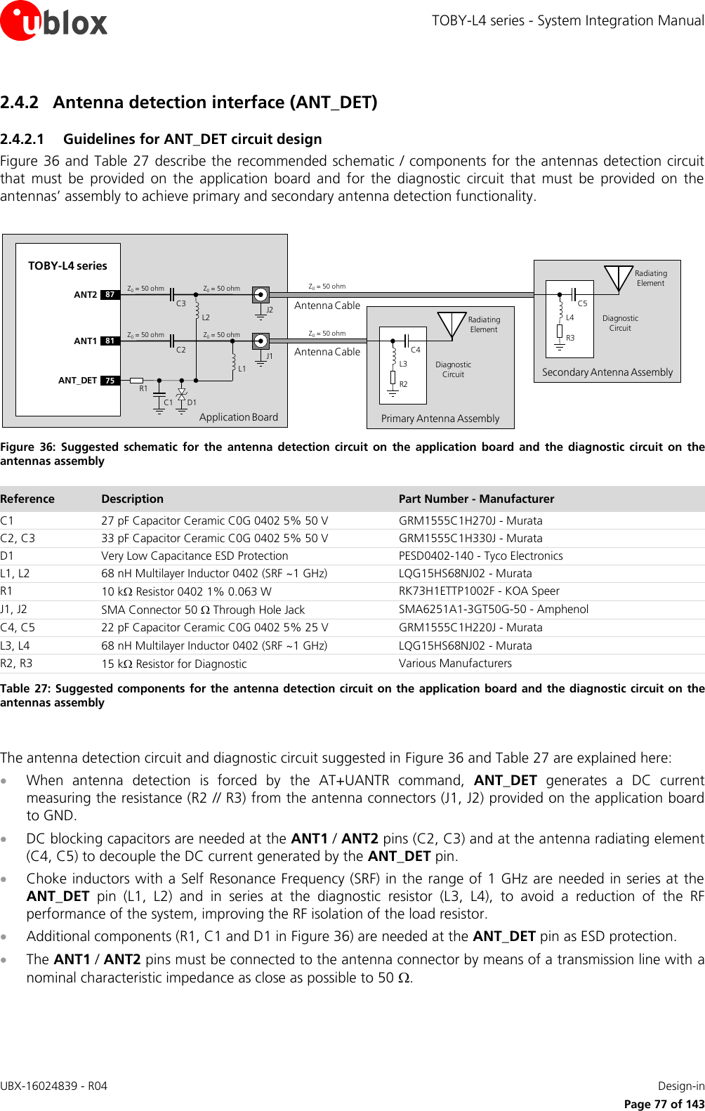
![TOBY-L4 series - System Integration Manual UBX-16024839 - R04 Design-in Page 78 of 143 The DC impedance at the RF port for some antennas may be a DC open (e.g. linear monopole) or a DC short to reference GND (e.g. PIFA antenna). For those antennas without the diagnostic circuit of Figure 36, the measured DC resistance is always at the limits of the measurement range (respectively open or short), and there is no means to distinguish between a defect on the antenna path with similar characteristics (respectively: removal of linear antenna or RF cable shorted to GND for a PIFA antenna). Furthermore, any other DC signal injected to the RF connection from an ANT connector to a radiating element will alter the measurement and produce invalid results for antenna detection. It is recommended to use an antenna with a built-in diagnostic resistor in the range from 5 k to 30 k to assure good antenna detection functionality and avoid a reduction of module RF performance. The choke inductor should exhibit a parallel Self Resonance Frequency (SRF) in the range of 1 GHz to improve the RF isolation of the load resistor. For example: Consider an antenna with a built-in DC load resistor of 15 k. Using the +UANTR AT command, the module reports the resistance value evaluated from the antenna connector provided on the application board to GND: Reported values close to the used diagnostic resistor nominal value (i.e. values from 13 k to 17 k if a 15 k diagnostic resistor is used) indicate that the antenna is properly connected. Values close to the measurement range maximum limit (approximately 50 k) or an open-circuit “over range” report (see the u-blox AT Commands Manual [2]) means that that the antenna is not connected or the RF cable is broken. Reported values below the measurement range minimum limit (1 k) indicate a short to GND at the antenna or along the RF cable. Measurement inside the valid measurement range and outside the expected range may indicate an incorrect connection, damaged antenna or wrong value of antenna load resistor for diagnostics. The reported value could differ from the real resistance value of the diagnostic resistor mounted inside the antenna assembly due to the antenna cable length, the antenna cable capacity or the measurement method used. If the primary / secondary antenna detection function is not required by the customer application, the ANT_DET pin can be left unconnected and the ANT1 / ANT2 pins can be directly connected to the related antenna connector by means of a 50 transmission line as illustrated in Figure 35. 2.4.2.2 Guidelines for ANT_DET layout design The recommended layout for the primary antenna detection circuit to be provided on the application board to achieve the primary antenna detection functionality, implementing the recommended schematic illustrated in Figure 36 and Table 27, is explained here: The ANT1 / ANT2 pins must be connected to the antenna connector by means of a 50 transmission line, implementing the design guidelines described in section 2.4.1 and the recommendations of the SMA connector manufacturer. DC blocking capacitor at ANT1 / ANT2 pins (C2, C3) must be placed in series to the 50 RF line. The ANT_DET pin must be connected to the 50 transmission line by means of a sense line. Choke inductors in series at the ANT_DET pin (L1, L2) must be placed so that one pad is on the 50 transmission line and the other pad represents the start of the sense line to the ANT_DET pin. The additional components (R1, C1 and D1) on the ANT_DET line must be placed as ESD protection.](https://usermanual.wiki/u-blox/1EHQ37NN.TempConfidential-TOBY-L4-SysIntegrManual-UBX-16024839/User-Guide-3759877-Page-78.png)
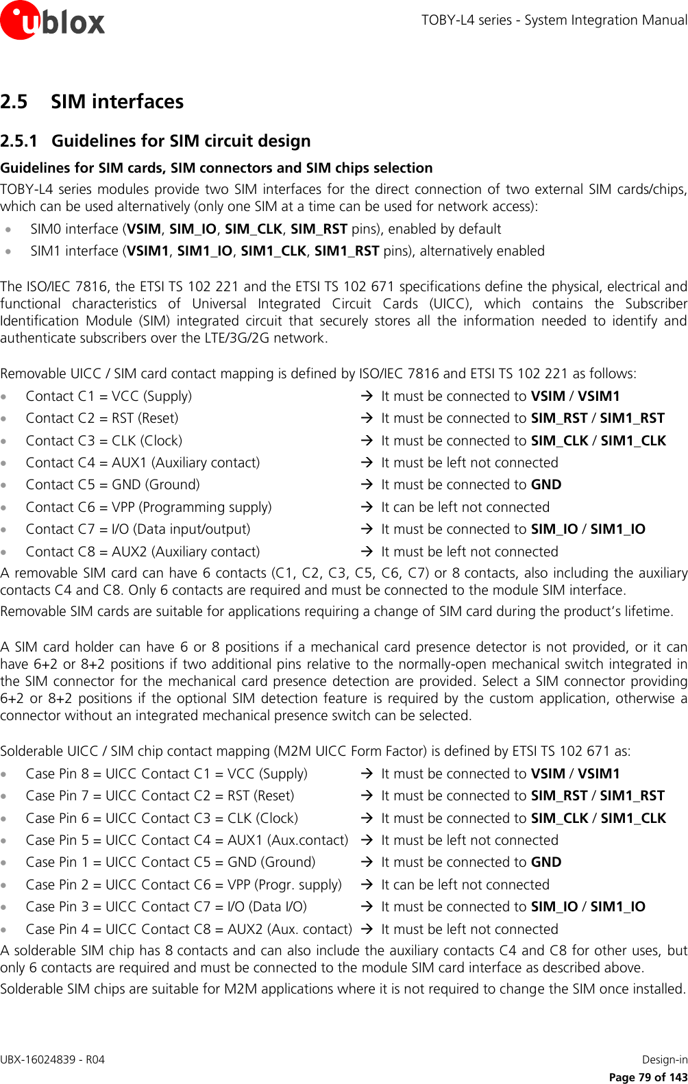
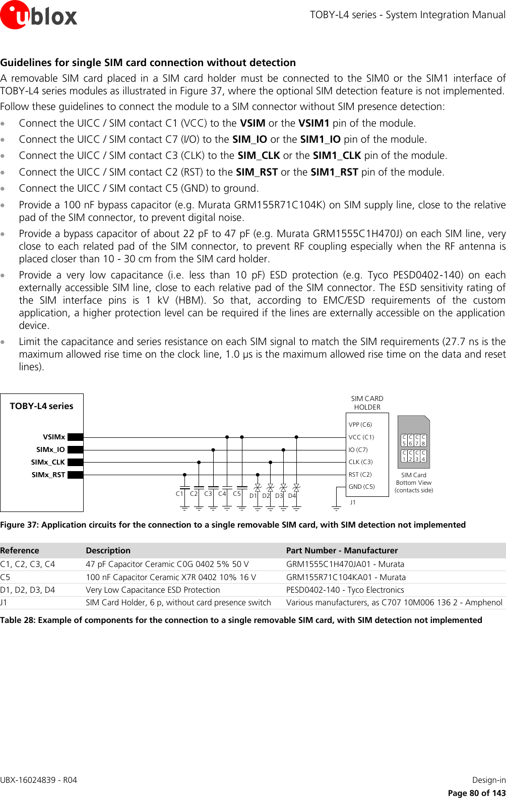
![TOBY-L4 series - System Integration Manual UBX-16024839 - R04 Design-in Page 83 of 143 Guidelines for dual SIM card / chip connection Two SIM cards / chips can be connected to the SIM interfaces of TOBY-L4 modules as illustrated in Figure 40. TOBY-L4 series modules do not support the usage of two SIMs at the same time, but two SIMs can be populated on the application board: connecting the first SIM to the SIM0 interface of the module and connecting the second SIM to the SIM1 interface of the module, as illustrated in Figure 40 top side In this case, the SIM interface and the related external SIM card / chip to be used can be selected by means of the AT+XSIMSWITCH command (see u-blox AT Commands Manual [2]) or by means of uCPU application, performing the SIM switch operation providing a suitable switch to connect only the first or only the second SIM at a time to the SIM0 interface of the module, as illustrated in Figure 40 bottom side In this case, if the SIM hot insertion / removal feature is enabled on the GPIO5 pin by AT commands (see sections 1.8.2 and 1.13, and the u-blox AT Commands Manual [2], +UGPIOC, +UDCONF=50 commands) or by means of uCPU application, than the switch from the first to the second external SIM can be properly done when a Low logic level is present on the GPIO5 pin (“SIM not inserted” = SIM interface not enabled), without the necessity of a module re-boot, so that the SIM interface will be re-enabled by the module to use the second SIM when a high logic level is re-applied on the GPIO5 pin. The application processor will drive the SIM switch using its own GPIO to properly select the SIM that is used by the module. Another GPIO may be used to handle the SIM hot insertion / removal function of TOBY-L4 series modules, which can also be handled by other external circuits or by the cellular module GPIO according to the application requirements. The dual SIM connection circuit illustrated in Figure 40 can be implemented for SIM chips as well. If it is required to switch between more than 2 SIMs, a circuit similar to the one illustrated in Figure 40 bottom side can be implemented, using suitable switches. Follow these guidelines to connect the module to two external UICC / SIM: Connect the contact C1 (VCC) of the first external UICC / SIM to the VSIM pin of the module and the one of the second external UICC / SIM to the VSIM1 pin of the module. Connect the contact C7 (I/O) of the first external UICC / SIM to the SIM_IO pin of the module and the one of the second external UICC / SIM to the SIM1_IO pin of the module. Connect the contact C3 (CLK) of the first external UICC / SIM to the SIM_CLK pin of the module and the one of the second external UICC / SIM to the SIM1_CLK pin of the module. Connect the contact C2 (RST) of the first external UICC / SIM to the SIM_RST pin of the module and the one of the second external UICC / SIM to the SIM1_RST pin of the module. Connect the contact C5 (GND) of each external UICC / SIM to ground. Provide a 100 nF bypass capacitor (e.g. Murata GRM155R71C104K) at the SIM supply (VSIM / VSIM1), close to the related pad of each external UICC / SIM, to prevent digital noise. Provide a bypass capacitor of about 22 pF to 47 pF (e.g. Murata GRM1555C1H470J) on each SIM line, very close to each related pad of each external SIM connector, to prevent RF coupling especially when the RF antenna is placed closer than 10 - 30 cm from the SIM card holders. Provide a very low capacitance (i.e. less than 10 pF) ESD protection (e.g. Tyco Electronics PESD0402-140) on each externally accessible SIM line, close to each pad of each external SIM connector, according to the EMC/ESD requirements of the custom application. Limit the capacitance and series resistance on each SIM signal to match the SIM requirements (20.5 ns is the maximum rise time on the clock line, 1.0 µs is the maximum rise time on the data and reset lines). If a circuit as the one illustrated in Figure 40 bottom side is implemented, use a suitable low on resistance (i.e. few ohms) and low on capacitance (i.e. few pF) 2-throw analog switch (e.g. Fairchild FSA2567) as SIM switch to ensure high-speed data transfer according to SIM requirements.](https://usermanual.wiki/u-blox/1EHQ37NN.TempConfidential-TOBY-L4-SysIntegrManual-UBX-16024839/User-Guide-3759877-Page-83.png)
![TOBY-L4 series - System Integration Manual UBX-16024839 - R04 Design-in Page 86 of 143 2.6 Data communication interfaces 2.6.1 USB interface 2.6.1.1 Guidelines for USB circuit design Different application circuits can be implemented for the USB interface according to specific use-case: USB 2.0 interface, with the module acting as USB device, as illustrated in Figure 41 and Table 32 USB 2.0 interface, with the module acting as USB host, as illustrated in Figure 42 and Table 33 USB 3.0 interface, with the module acting as USB device, as illustrated in Figure 43 and Table 34 USB pull-up or pull-down resistors and external series resistors on the USB_D+ and USB_D– lines as required by the USB 2.0 specification [3] are part of the module USB pins driver and do not need to be externally provided. Series DC decoupling capacitors are internally provided on the USB_SSTX+ and USB_SSTX– lines as required by the USB 3.0 specification [4] and do not need to be externally provided. The USB_SSTX+/USB_SSTX– USB Super-Speed differential transmitter data output lines of the module must be connected to the USB Super-Speed differential receiver data input lines of the external USB 3.0 host. The USB_SSRX+/USB_SSRX– USB Super-Speed differential receiver data input lines of the module must be connected to the USB Super-Speed differential transmitter data output lines of the external USB 3.0 host, with series DC decoupling capacitors being provided on the host side as per the USB 3.0 specification [4]. Routing the USB pins to a connector, they will be externally accessible on the application device. According to the EMC/ESD requirements of the application, an additional ESD protection device with very low capacitance should be provided close to the accessible point on the line connected to this pin. The USB interface pins ESD sensitivity rating is 1 kV (Human Body Model according to JESD22-A114F). A higher protection level could be required if the lines are externally accessible and it can be achieved by mounting a very low capacitance (i.e. less or equal to 1 pF) ESD protection (e.g. Tyco Electronics PESD0402-140 ESD protection device) on the lines connected to these pins, close to the accessible points. The USB pins of the modules can be directly connected to the USB host application processor without additional ESD protections if they are not externally accessible or according to EMC/ESD requirements. D+D–GND28 USB_D+27 USB_D–GNDUSB 2.0 DEVICE CONNECTORVBUSD+D–GNDUSB 2.0 HOST PROCESSORTOBY-L4 series VBUS4VUSB_DETD1 D2 D3 C1 C128 USB_D+27 USB_D–GNDTOBY-L4 series 4VUSB_DET168 USB_ID168 USB_ID170 USB_SSRX+171 USB_SSRX–175 USB_SSTX+176 USB_SSTX–170 USB_SSRX+171 USB_SSRX–175 USB_SSTX+176 USB_SSTX– Figure 41: USB 2.0 interface application circuits, with TOBY-L4 series module acting as a USB device Reference Description Part Number - Manufacturer C1 100 nF Capacitor Ceramic X7R 0402 10% 16 V GRM155R61A104KA01 - Murata D1, D2, D3 Very Low Capacitance ESD Protection PESD0402-140 - Tyco Electronics Table 32: Component for USB 2.0 interface application circuits, with TOBY-L4 series module acting as a USB device](https://usermanual.wiki/u-blox/1EHQ37NN.TempConfidential-TOBY-L4-SysIntegrManual-UBX-16024839/User-Guide-3759877-Page-86.png)
![TOBY-L4 series - System Integration Manual UBX-16024839 - R04 Design-in Page 88 of 143 2.6.1.2 Guidelines for USB layout design The USB_D+/USB_D–, USB_SSTX+/USB_SSTX– and USB_SSRX+/USB_SSRX– lines require accurate layout design to achieve reliable signaling at the high speed data rates (up to 480 Mbit/s or up to 5 Gbit/s) supported by the USB 2.0 or USB 3.0 interface. The characteristic impedance of the USB_D+/USB_D–, USB_SSTX+/USB_SSTX– and USB_SSRX+/USB_SSRX– lines is specified by the USB 2.0 specification [3] and the USB 3.0 specification [4]. The most important parameter is the differential characteristic impedance applicable for the odd-mode electromagnetic field, which should be as close as possible to 90 differential. Signal integrity may be degraded if the PCB layout is not optimal, especially when the USB signaling lines are very long. Use the following general routing guidelines to minimize signal quality problems: Route USB_D+/USB_D–, USB_SSTX+/USB_SSTX– and USB_SSRX+/USB_SSRX– lines as a differential pair Route USB_D+/USB_D–, USB_SSTX+/USB_SSTX– and USB_SSRX+/USB_SSRX– lines as short as possible Ensure the differential characteristic impedance (Z0) is as close as possible to 90 Ensure the common mode characteristic impedance (ZCM) is as close as possible to 30 Consider design rules for USB_D+/USB_D–, USB_SSTX+/USB_SSTX– and USB_SSRX+/USB_SSRX– similar to RF transmission lines, these being coupled differential micro-strip or buried stripline: avoid any stubs, abrupt change of layout, and route on clear PCB area Figure 44 and Figure 45 provide two examples of coplanar waveguide designs with differential characteristic impedance close to 90 and common mode characteristic impedance close to 30 . The first transmission line can be implemented for a 4-layer PCB stack-up herein illustrated; the second transmission line can be implemented for a 2-layer PCB stack-up herein illustrated. 35 µm35 µm35 µm35 µm270 µm270 µm760 µmL1 CopperL3 CopperL2 CopperL4 CopperFR-4 dielectricFR-4 dielectricFR-4 dielectric350 µm 400 µm400 µm350 µm400 µm Figure 44: Example of USB line design, with Z0 close to 90 and ZCM close to 30 , for the described 4-layer board layup 35 µm35 µm1510 µmL2 CopperL1 CopperFR-4 dielectric740 µm 410 µm410 µm740 µm410 µm Figure 45: Example of USB line design, with Z0 close to 90 and ZCM close to 30 , for the described 2-layer board layup](https://usermanual.wiki/u-blox/1EHQ37NN.TempConfidential-TOBY-L4-SysIntegrManual-UBX-16024839/User-Guide-3759877-Page-88.png)
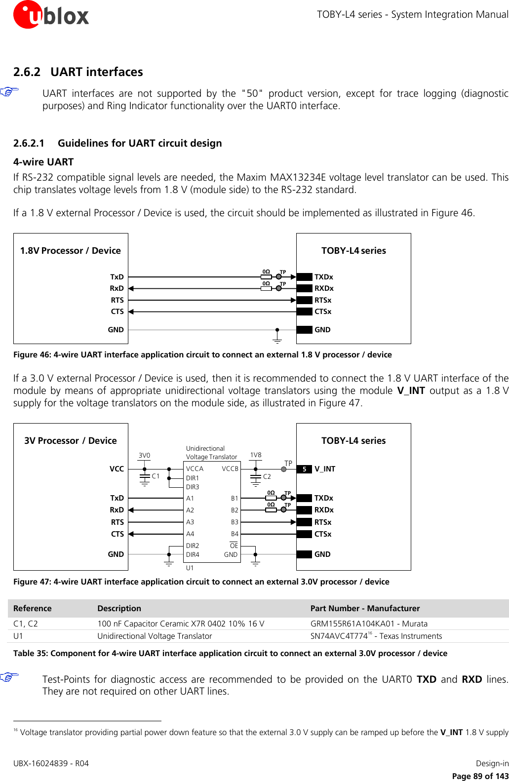
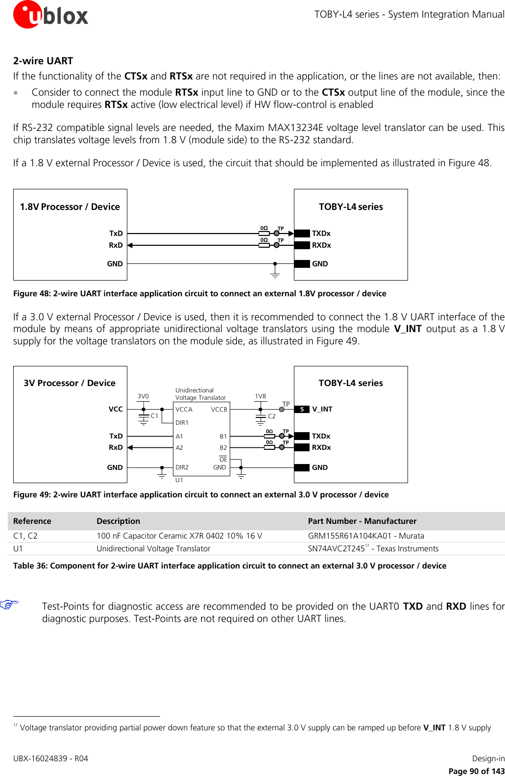
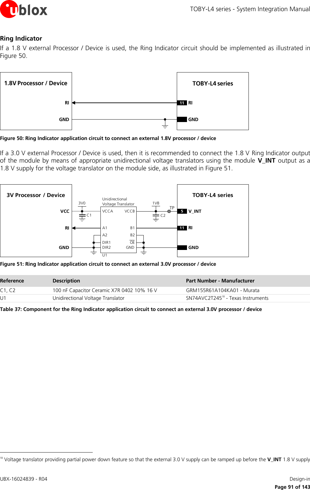
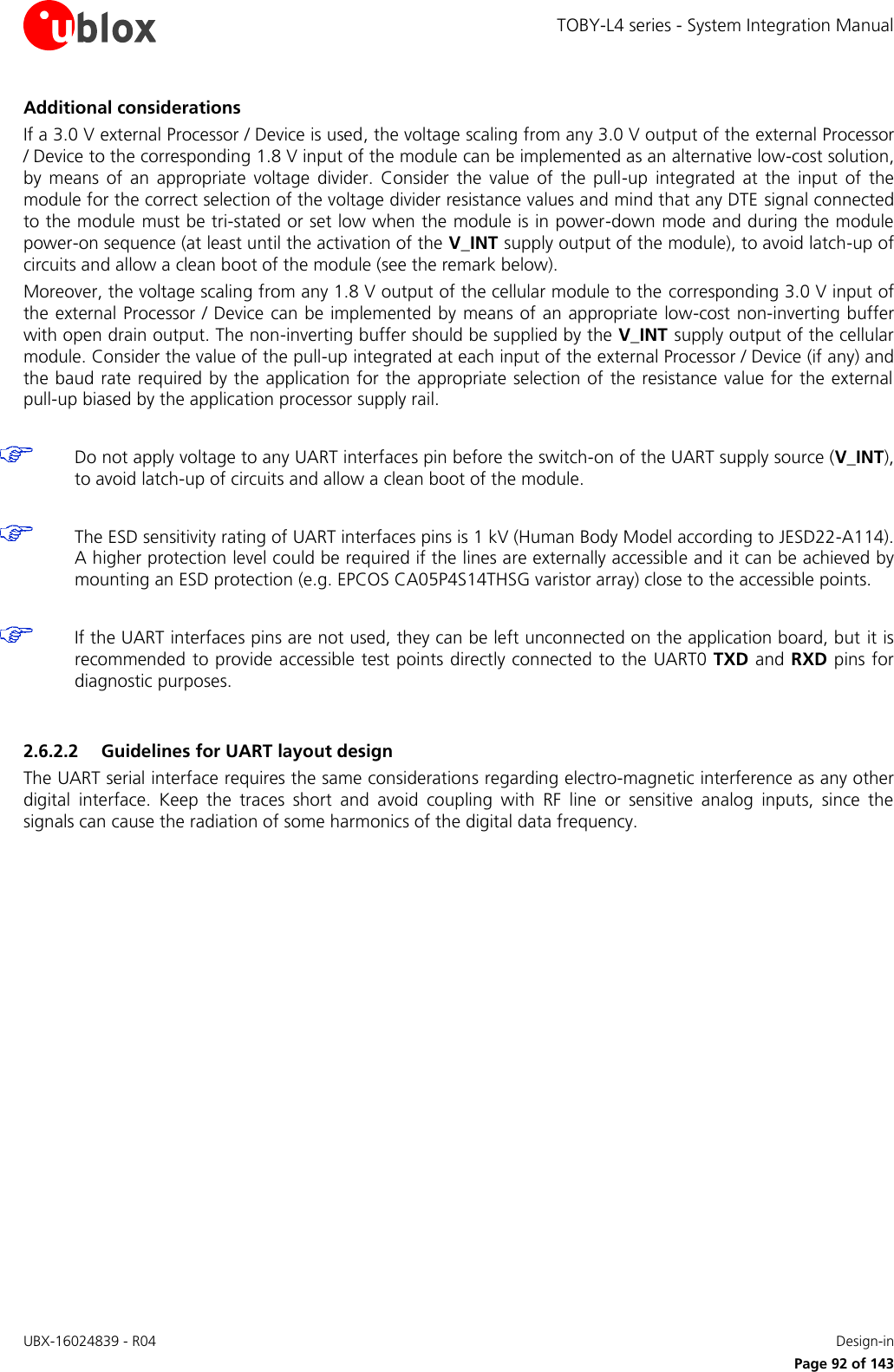
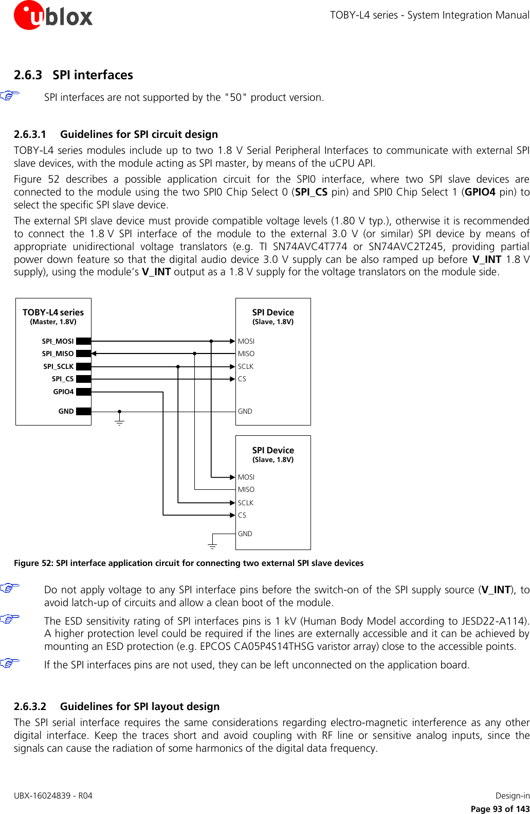
![TOBY-L4 series - System Integration Manual UBX-16024839 - R04 Design-in Page 94 of 143 2.6.4 DDC (I2C) interfaces DDC (I2C) interfaces are not supported by the "50" product version. 2.6.4.1 General guidelines for DDC (I2C) circuit design The DDC I2C-bus pins of the module are open drain outputs conforming to the I2C bus specifications [6]. External pull-up resistors to a suitable 1.8 V supply (e.g. V_INT) are required for operations: for example, 4.7 k resistors can be commonly used. Connect the DDC (I2C) pull-ups to the V_INT 1.8 V supply source, or another 1.8 V supply source enabled after V_INT (e.g., as the GNSS 1.8 V supply present in Figure 54 application circuit), as any external signal connected to the DDC (I2C) interface must not be set high before the switch-on of the V_INT supply of DDC (I2C) pins, to avoid latch-up of circuits and allow a clean boot of the module. The signal shape is defined by the values of the pull-up resistors and the bus capacitance. Long wires on the bus will increase the capacitance. If the bus capacitance is increased, use pull-up resistors with a nominal resistance value lower than 4.7 k, to match the I2C bus specifications [6] regarding the rise and fall times of the signals. Figure 53 and Table 38 describe typical application circuits for connecting TOBY-L4 series modules to 1.8 V I2C devices (see Figure 53 top side) or 3 V I2C devices (see Figure 53 bottom side). 1.8V I2C DeviceSDASCL1V85V_INTR1 R21V8 1V8SDAxSCLxTOBY-L4 seriesR1 R23V0SDAxSCLxR3 R41V8SDA_A SDA_BGNDU1SCL_ASCL_BVCCAVCCBI2C-bus Bidirectional Voltage Translator5V_INTC1 C2SDASCLOEGND GND3V I2C Device TOBY-L4 seriesGND GND Figure 53: Application circuit for connecting TOBY-L4 series modules to 1.8 V or 3 V I2C devices Reference Description Part Number - Manufacturer R1, R2, R3, R4 4.7 k Resistor 0402 5% 0.1 W RC0402JR-074K7L - Yageo Phycomp C1, C2 100 nF Capacitor Ceramic X7R 0402 10% 16 V GRM155R71C104KA01 - Murata U1 I2C-bus Bidirectional Voltage Translator TCA9406DCUR19 - Texas Instruments Table 38: Components for connecting TOBY-L4 series modules to 1.8 V or 3 V I2C devices The ESD sensitivity rating of the DDC (I2C) pins is 1 kV (Human Body Model according to JESD22-A114). A higher protection level could be required if the lines are externally accessible and it can be achieved by mounting an ESD protection (e.g. EPCOS CA05P4S14THSG varistor array) close to the accessible points. If the pins are not used as DDC bus interface, they can be left unconnected. 19 Voltage translator providing partial power down feature so that the external 3 V supply can be also ramped up before V_INT 1.8 V supply](https://usermanual.wiki/u-blox/1EHQ37NN.TempConfidential-TOBY-L4-SysIntegrManual-UBX-16024839/User-Guide-3759877-Page-94.png)
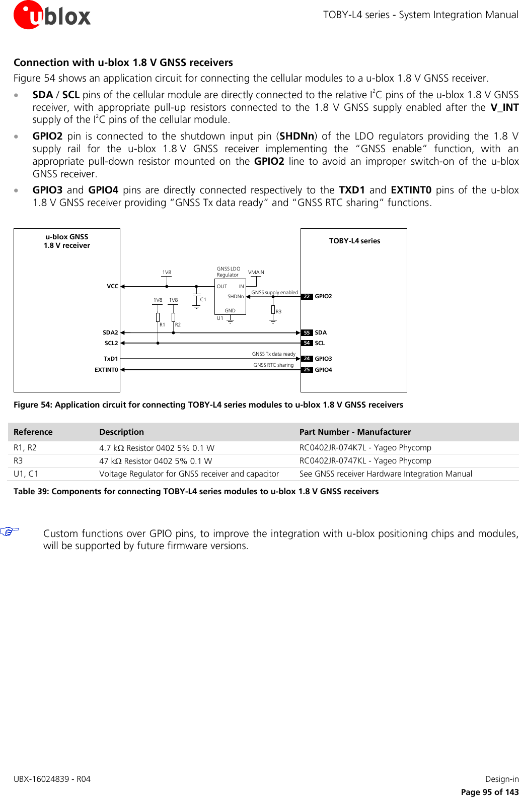
![TOBY-L4 series - System Integration Manual UBX-16024839 - R04 Design-in Page 96 of 143 Figure 55 illustrates an alternative application circuit solution in which the cellular module supplies a u-blox 1.8 V GNSS receiver. The V_INT 1.8 V regulated supply output of the cellular module can be used as supply source for a u-blox 1.8 V GNSS receiver (u-blox 6 generation receiver or newer) instead of using an external voltage regulator, as shown in Figure 54. The V_INT supply is able to support the maximum current consumption of these positioning receivers. The internal switching step-down regulator that generates the V_INT supply is set to 1.8 V (typical) when the cellular module is switched on and it is disabled when the module is switched off. The supply of the u-blox 1.8 V GNSS receiver can be switched off using an external p-channel MOS controlled by the GPIO2 pin of the cellular modules by means of a suitable inverting transistor as shown in Figure 55, implementing the “GNSS supply enable” function. If this feature is not required, the V_INT supply output can be directly connected to the u-blox 1.8 V GNSS receiver, so that it will switch on when V_INT output is enabled. According to the V_INT supply output voltage ripple characteristic specified in the TOBY-L4 series Data Sheet [1]: Additional filtering may be needed to properly supply an external LNA, depending on the characteristics of the used LNA, adding a series ferrite bead and a bypass capacitor (e.g. the Murata BLM15HD182SN1 ferrite bead and the Murata GRM1555C1H220J 22 pF capacitor) at the input of the external LNA supply line. u-blox GNSS1.8 V receiverTxD1SDA2SCL2VCC1V8C1R35V_INTR5R4TPT2T1R1 R21V8 1V8GNSS data readyGNSS supply enabled 22 GPIO2SDASCLGPIO3555424TOBY-L4 seriesEXTINT0 GPIO425GNSS RTC sharing Figure 55: Application circuit for connecting TOBY-L4 series modules to u-blox 1.8 V GNSS receivers using V_INT as supply Reference Description Part Number - Manufacturer R1, R2 4.7 k Resistor 0402 5% 0.1 W RC0402JR-074K7L - Yageo Phycomp R3 47 k Resistor 0402 5% 0.1 W RC0402JR-0747KL - Yageo Phycomp R4 10 k Resistor 0402 5% 0.1 W RC0402JR-0710KL - Yageo Phycomp R5 100 k Resistor 0402 5% 0.1 W RC0402JR-07100KL - Yageo Phycomp T1 P-Channel MOSFET Low On-Resistance IRLML6401 - International Rectifier or NTZS3151P - ON Semi T2 NPN BJT Transistor BC847 - Infineon C1 100 nF Capacitor Ceramic X7R 0402 10% 16 V GRM155R71C104KA01 - Murata Table 40: Components for connecting TOBY-L4 series modules to u-blox 1.8 V GNSS receivers using V_INT as supply Custom functions over GPIO pins, to improve the integration with u-blox positioning chips and modules, will be supported by future firmware versions.](https://usermanual.wiki/u-blox/1EHQ37NN.TempConfidential-TOBY-L4-SysIntegrManual-UBX-16024839/User-Guide-3759877-Page-96.png)
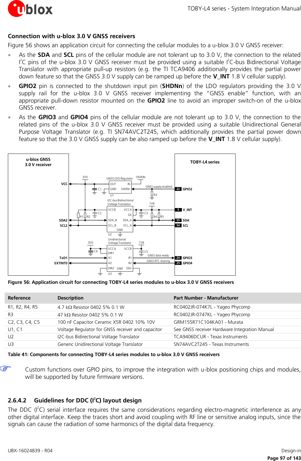
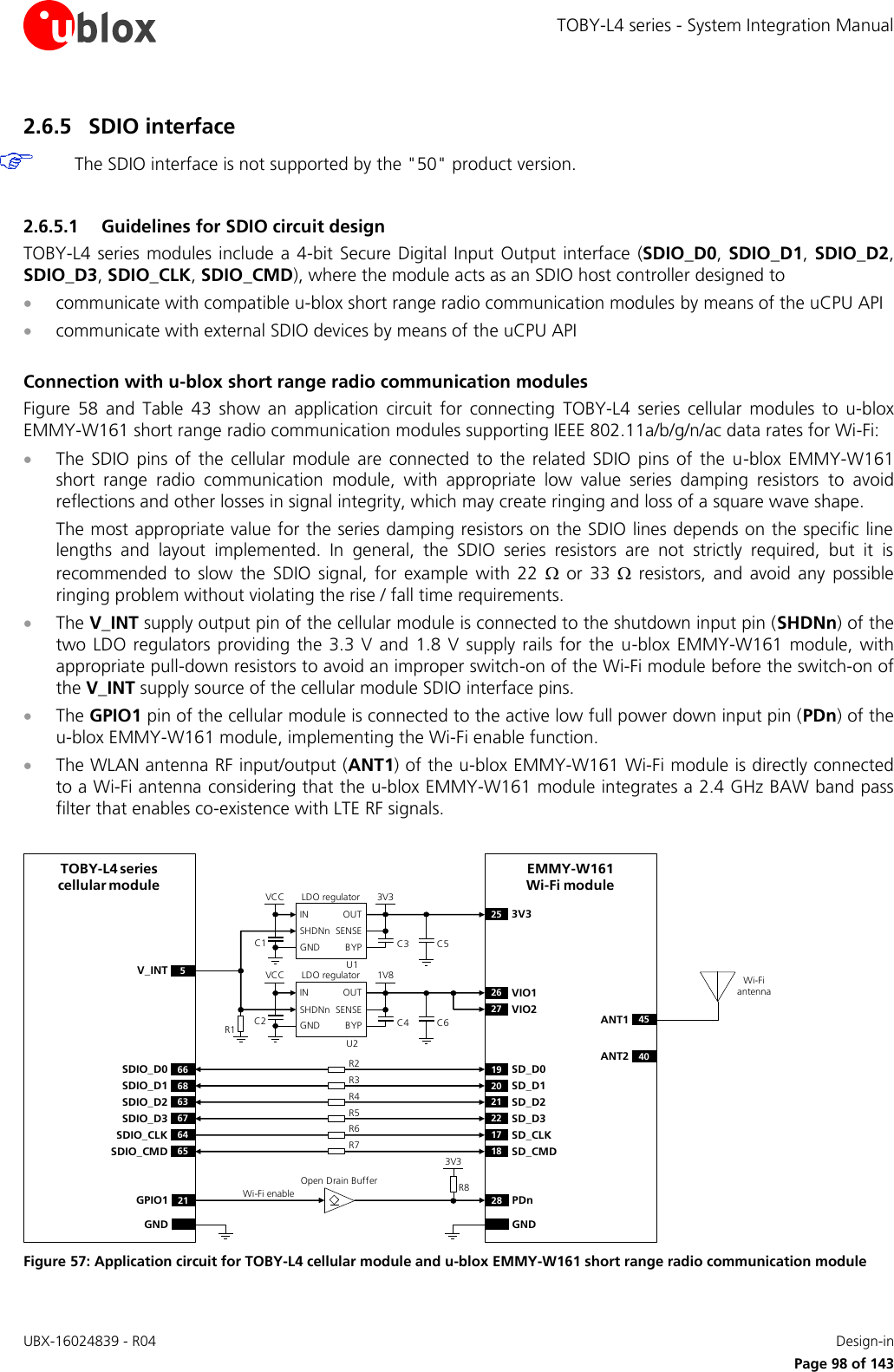
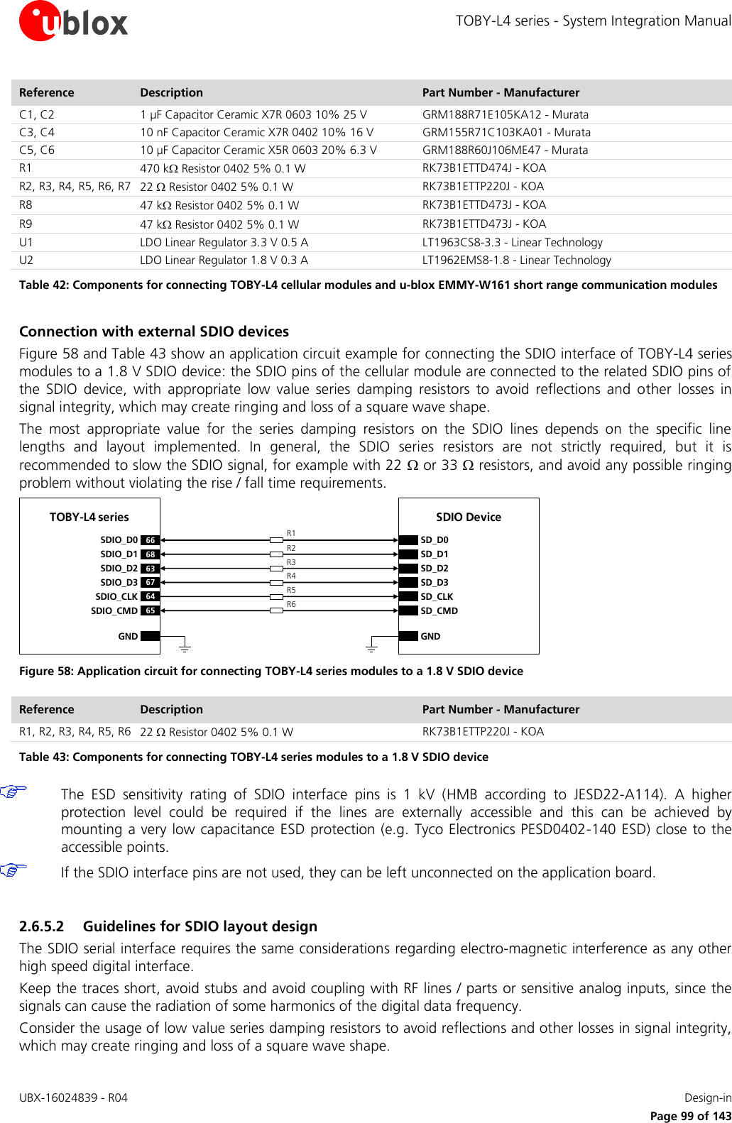
![TOBY-L4 series - System Integration Manual UBX-16024839 - R04 Design-in Page 100 of 143 2.6.6 RGMII interface The RGMII interface is not supported by the "50" product version. 2.6.6.1 Guidelines for RGMII circuit design TOBY-L4 series modules include an Ethernet Media Access Control (MAC) block supporting up to 1 Gbit/s data rate via a Reduced Gigabit Media-Independent Interface compliant with the RGMII Version 1.3 specification [7] and the RMII Revision 1.2 specification [8]. The module represents an Ethernet MAC controller, which can be connected to a compatible external Ethernet physical transceiver (PHY) chip to provide communication over Ethernet as illustrated in Figure 59. Recommended compatible Ethernet PHY chips are: Marvell 88E1510 Marvell 88E1512 TOBY-L4 seriesEthernet MACRGMIIConnectorEthernet PHYUnshielded Twisted Pair Figure 59: RGMII interface application circuit block diagram The ESD sensitivity rating of RGMII interface pins is 1 kV (HMB according to JESD22-A114). A higher protection level could be required if the lines are externally accessible and it can be achieved by mounting a very low capacitance ESD protection (e.g. Tyco Electronics PESD0402-140 ESD) close to the accessible points. If the RGMII interface pins are not used, they can be left unconnected on the application board. 2.6.6.2 Guidelines for RGMII layout design The RGMII / RMII interface requires the same considerations regarding electro-magnetic interference as any other high speed digital interface. Keep the traces short, avoid stubs and avoid coupling with RF lines / parts or sensitive analog inputs, since the signals can cause the radiation of some harmonics of the digital data frequency. Consider the usage of low value series damping resistors to avoid reflections and other losses in signal integrity, which may create ringing and loss of a square wave shape.](https://usermanual.wiki/u-blox/1EHQ37NN.TempConfidential-TOBY-L4-SysIntegrManual-UBX-16024839/User-Guide-3759877-Page-100.png)
![TOBY-L4 series - System Integration Manual UBX-16024839 - R04 Design-in Page 101 of 143 2.7 eMMC interface The eMMC interface is not supported by the "50" product version. 2.7.1.1 Guidelines for eMMC circuit design TOBY-L4 series modules include a 4-bit embedded Multi-Media Card interface compliant with JESD84-B451 Embedded Multimedia Card (eMMC) Electrical Standard 4.51 [9], which can be handled by means of the uCPU API. The eMMC interface can be connected to an external eMMC / SD memory as defined by the standard. Pull-up resistors can be added on MMC_D0, MMC_D1, MMC_D2 and MMC_D3 data lines, the MMC_CLK clock line and the MMC_CMD command line, to increase the rise time on the signals so as to compensate for any capacitance on the board, even if not strictly required. The ESD sensitivity rating of eMMC interface pins is 1 kV (HMB according to JESD22-A114). A higher protection level could be required if the lines are externally accessible and it can be achieved by mounting a very low capacitance ESD protection (e.g. Tyco Electronics PESD0402-140 ESD) close to the accessible points. If the eMMC interface pins are not used, they can be left unconnected on the application board. 2.7.1.2 Guidelines for eMMC layout design The eMMC interface requires the same considerations regarding electro-magnetic interference as any other high speed digital interface. Keep the traces short, avoid stubs and avoid coupling with RF lines / parts or sensitive analog inputs, since the signals can cause the radiation of some harmonics of the digital data frequency. Consider the usage of low value series damping resistors to avoid reflections and other losses in signal integrity, which may create ringing and loss of a square wave shape.](https://usermanual.wiki/u-blox/1EHQ37NN.TempConfidential-TOBY-L4-SysIntegrManual-UBX-16024839/User-Guide-3759877-Page-101.png)
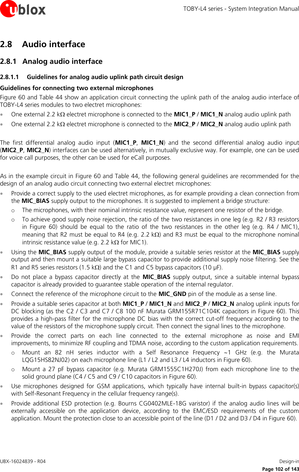
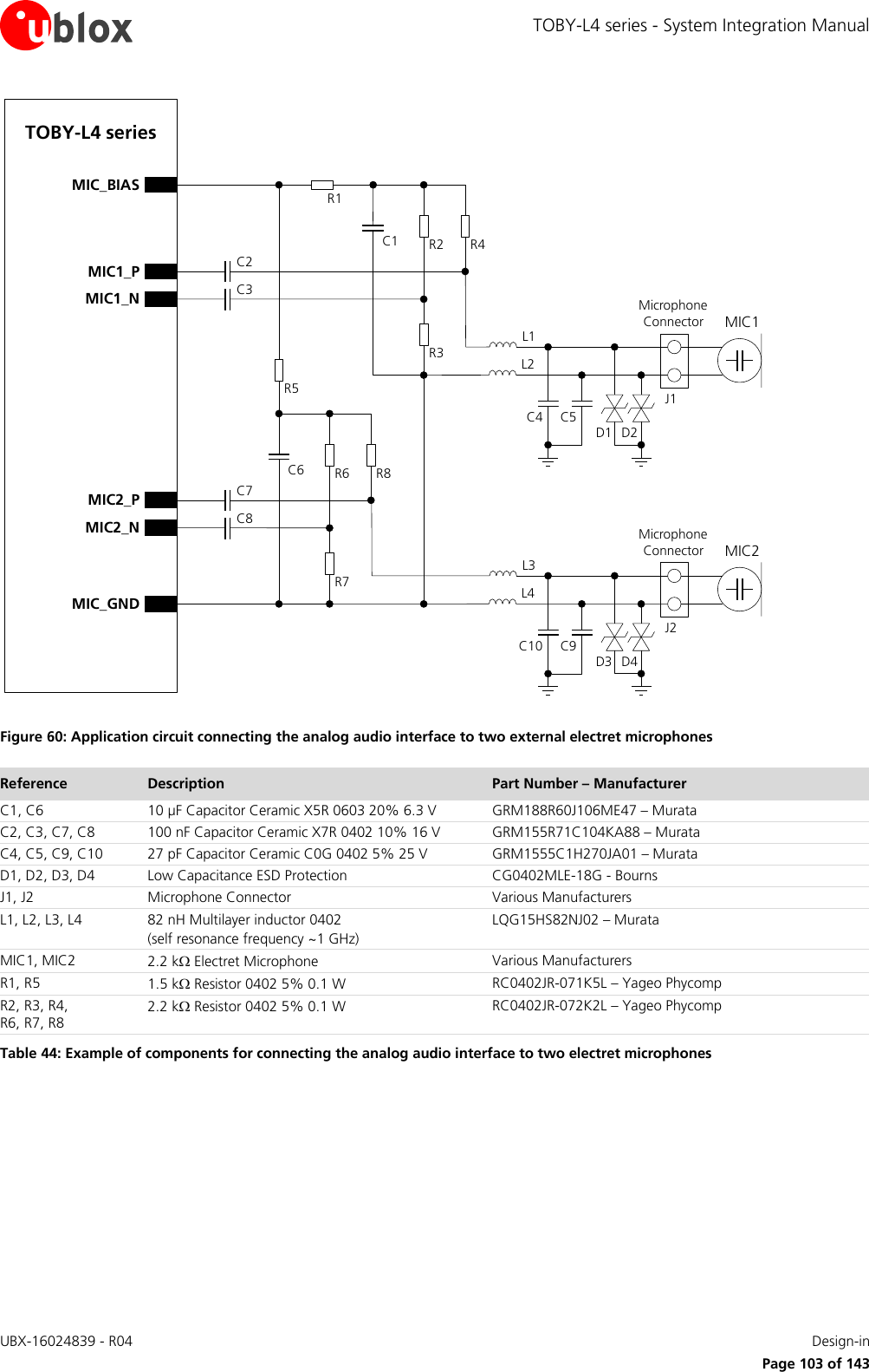
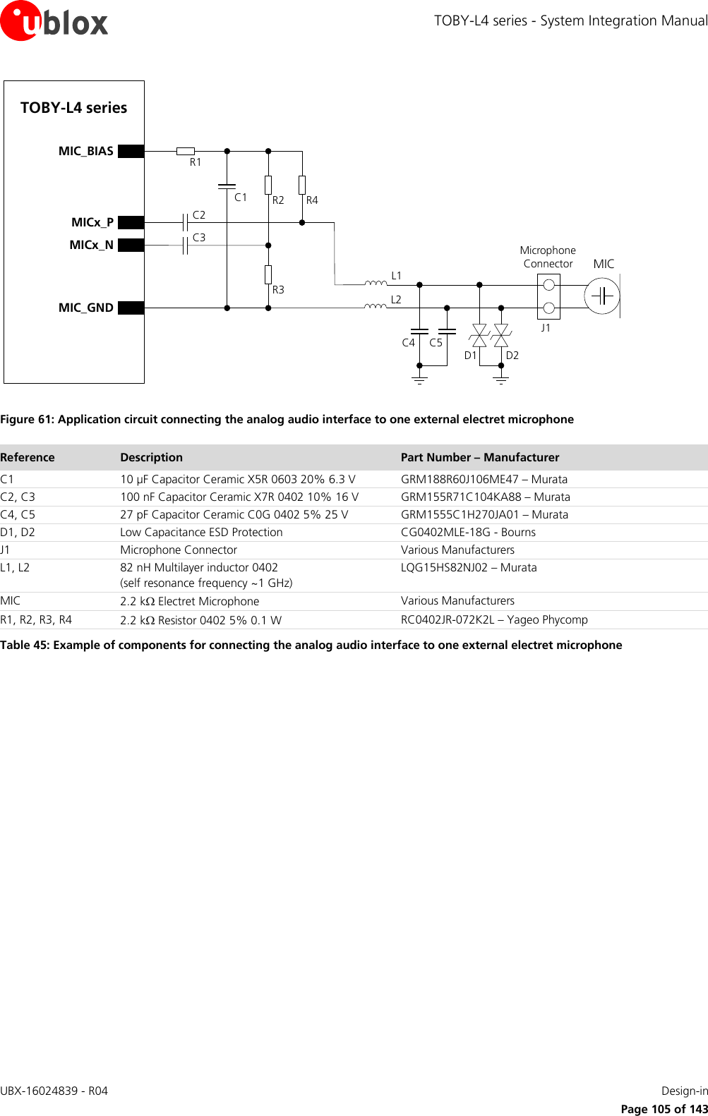
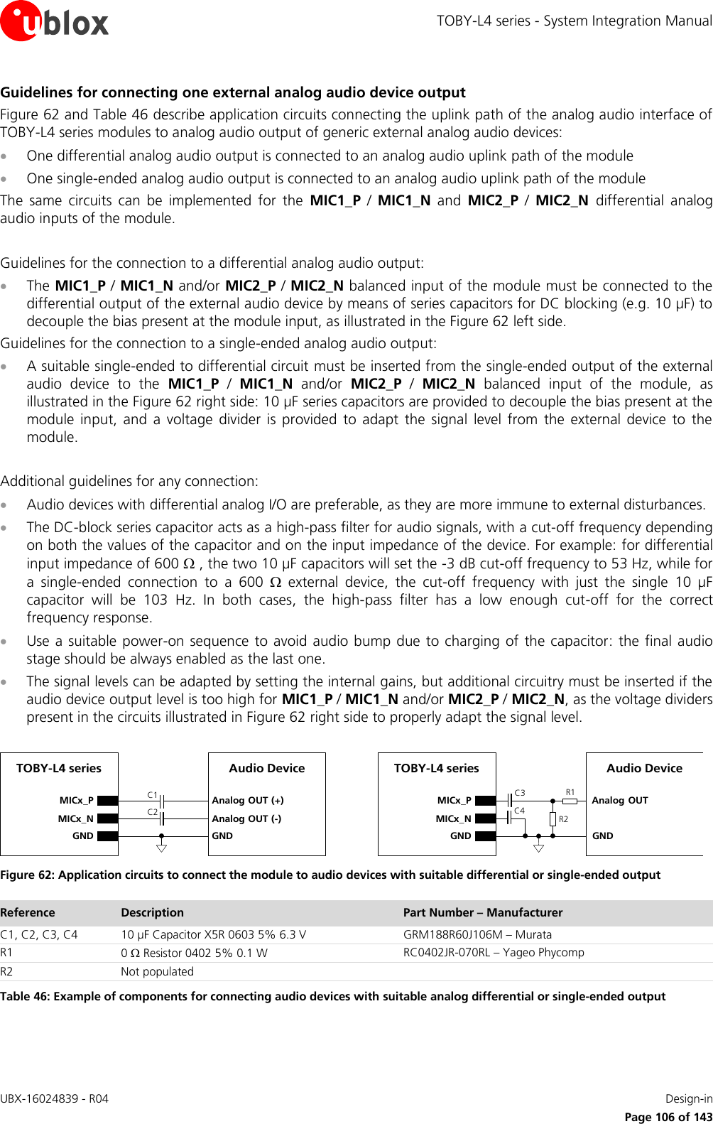
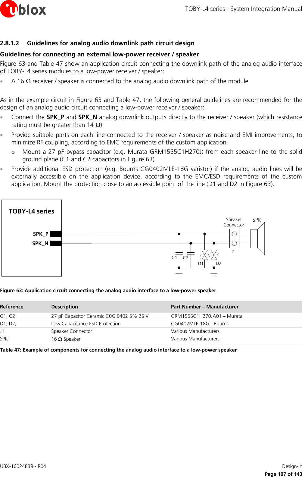
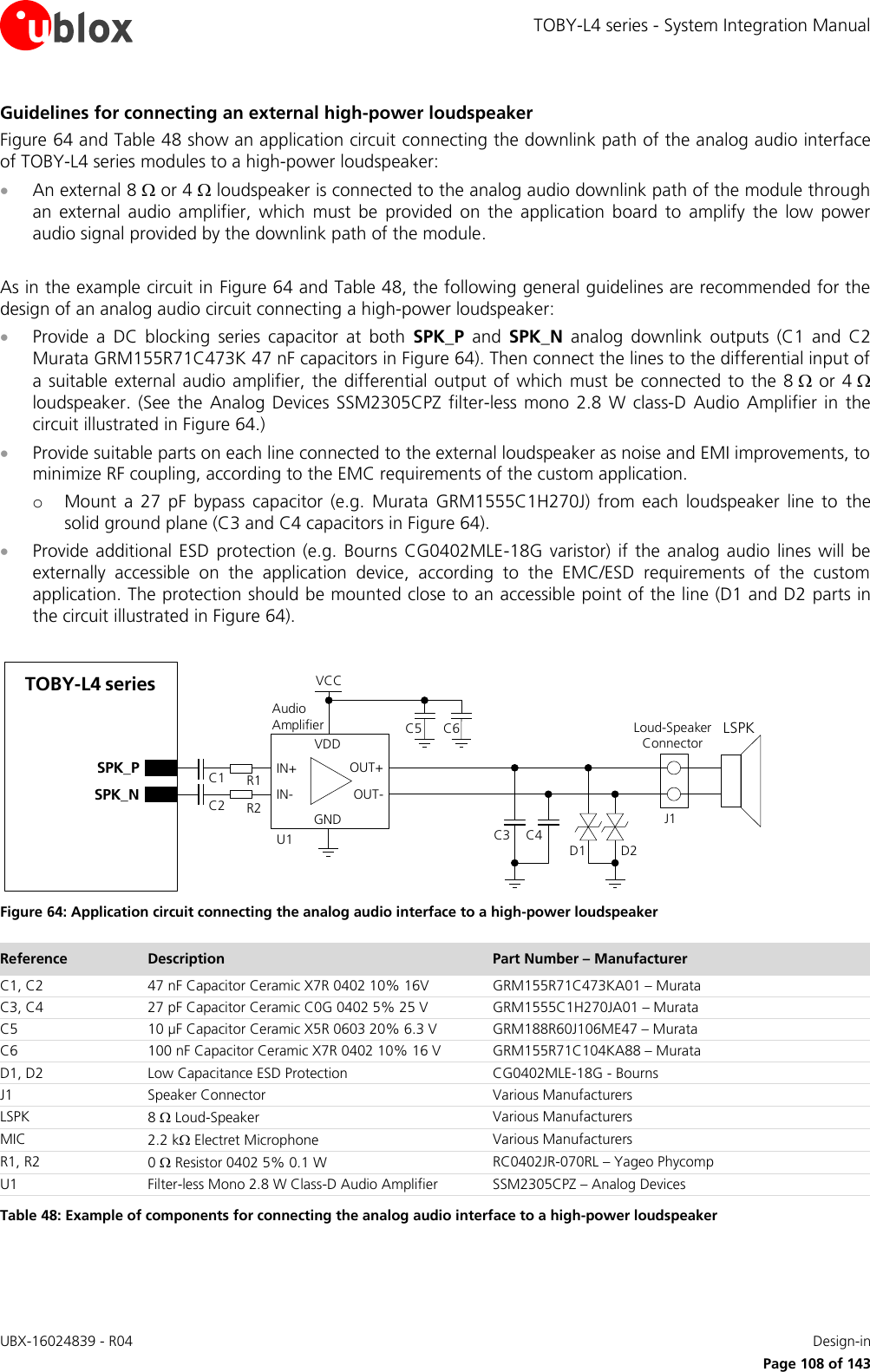
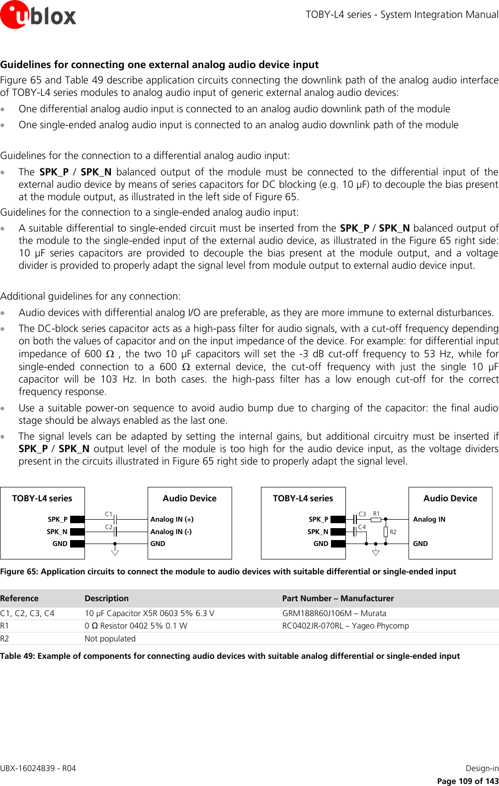
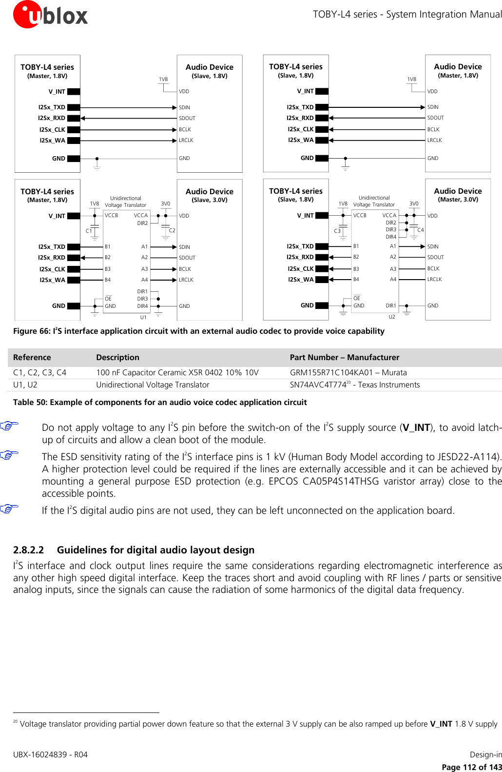
![TOBY-L4 series - System Integration Manual UBX-16024839 - R04 Design-in Page 113 of 143 2.9 ADC interfaces The ADC pins are not supported by the "50" product version. 2.9.1.1 Guidelines for ADC circuit design TOBY-L4 series modules include Analog to Digital Converter inputs (ADC1, ADC2), which can be handled by means of the dedicated uCPU API. The ADC pins can be connected to external circuits for general purpose voltage measurements. The voltage value at the ADC input must be within the range reported in the TOBY-L4 series Data Sheet [1]. If an external voltage divider is implemented to increase the measurement voltage range, check the input resistance of the ADC inputs reported in the TOBY-L4 series Data Sheet [1]: if the Thévenin's equivalent of the external circuit has a significant value as compared to the input resistance of the ADC inputs, this should be taken into account and corrected to properly associate the ADC response to the voltage source value, implementing an appropriate ADC calibration procedure. The ESD sensitivity rating of ADC interface pins is 1 kV (Human Body Model according to JESD22-A114). A higher protection level could be required if the lines are externally accessible and it can be achieved by mounting an ESD protection (e.g. EPCOS CA05P4S14THSG varistor array) close to the accessible points. If the ADC pins are not used, they can be left unconnected on the application board. 2.9.1.2 Guidelines for ADC layout design The Analog to Digital Converters (ADC1, ADC2) are high impedance analog inputs. The conversion accuracy will be degraded if noise is injected. Low-pass filter may be used to improve noise rejection; typically L-C tuned for RF rejection gives better results.](https://usermanual.wiki/u-blox/1EHQ37NN.TempConfidential-TOBY-L4-SysIntegrManual-UBX-16024839/User-Guide-3759877-Page-113.png)
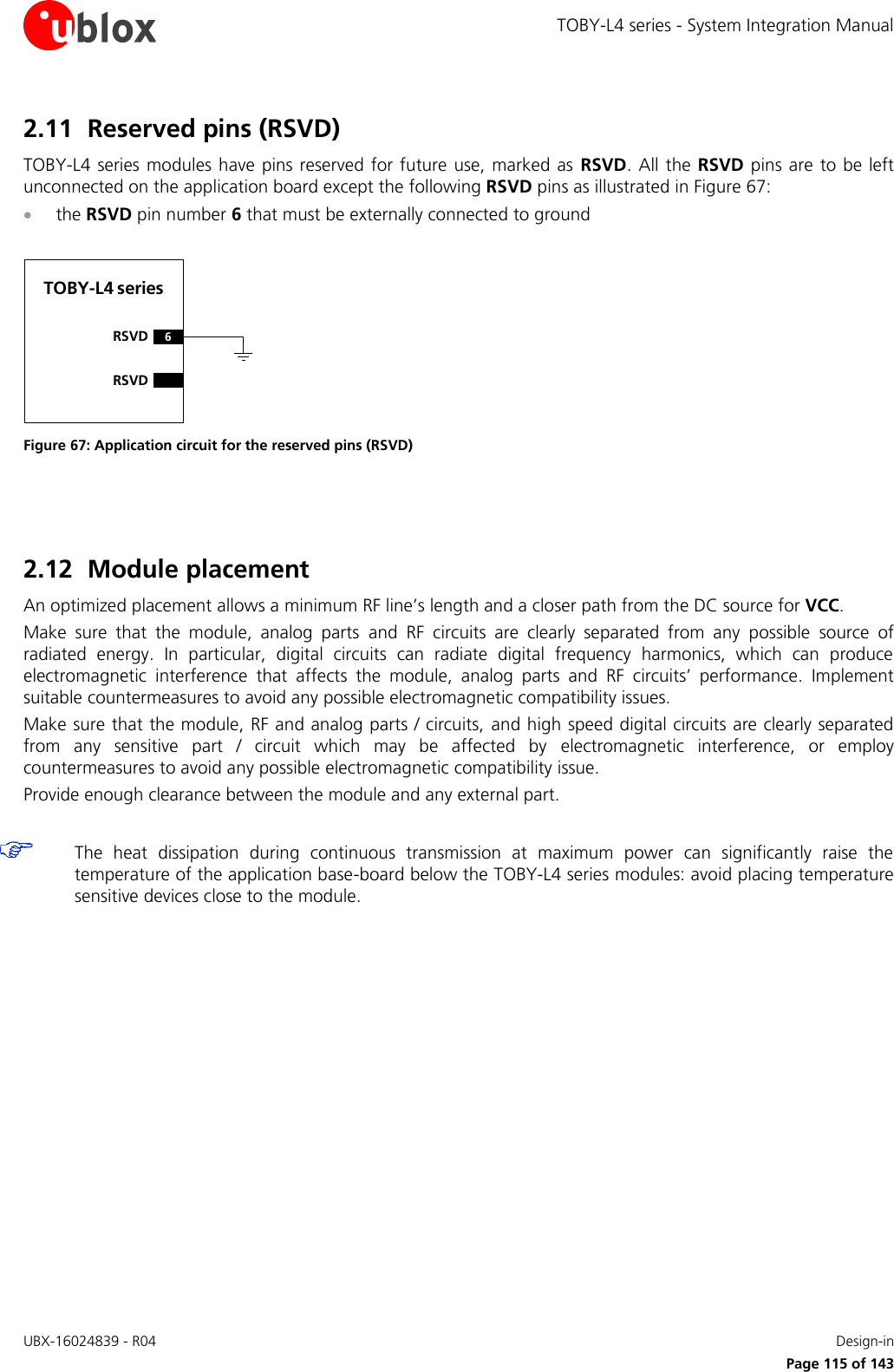
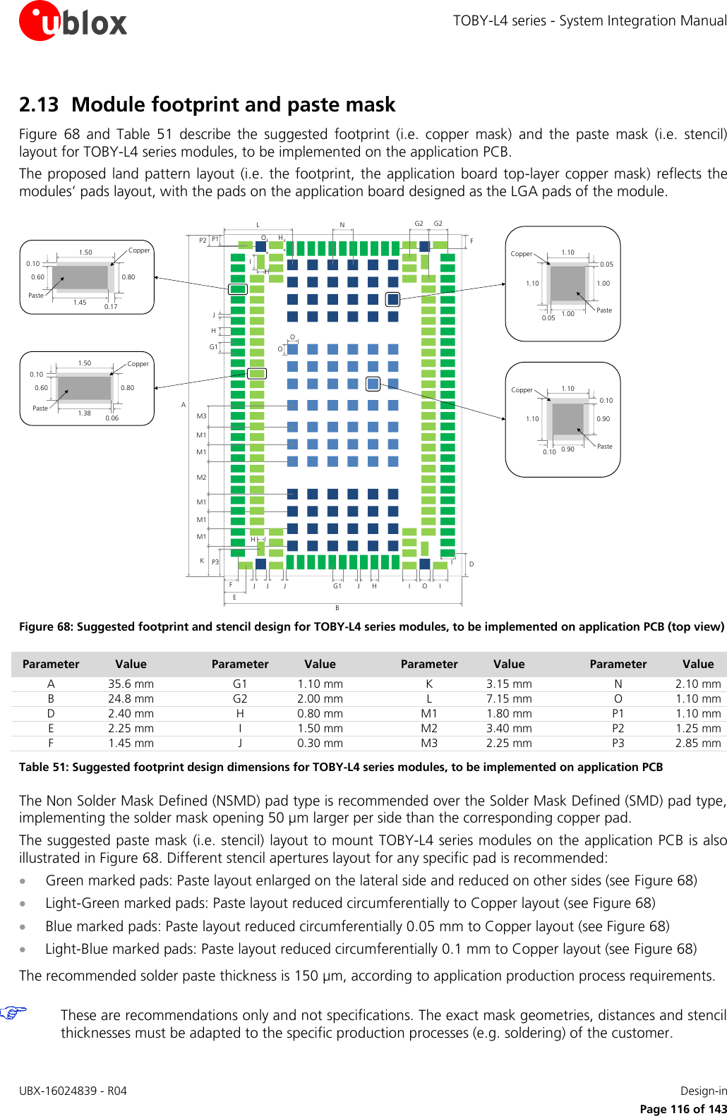
![TOBY-L4 series - System Integration Manual UBX-16024839 - R04 Design-in Page 117 of 143 2.14 Thermal guidelines Modules’ temperature range and thermal parameters are specified in the TOBY-L4 series Data Sheet [1]. The most critical condition concerning module thermal performance is the uplink transmission at maximum power (data upload in connected mode), because when the baseband processor runs at full speed, radio circuits are all active and the RF power amplifier is driven to higher output RF power. This scenario is not often encountered in real networks (for example, see the Terminal Tx Power distribution for WCDMA, taken from operation on a live network, described in the GSMA TS.09 Battery Life Measurement and Current Consumption Technique [10]); however the application should be correctly designed to cope with it. During transmission at maximum RF power, the TOBY-L4 series modules generate thermal power that may exceed 4 W in the worst case condition: this is an indicative value since the exact generated power strictly depends on operating conditions such as the actual antenna return loss, the number of allocated TX resource blocks, the transmitting frequency band, etc. The generated thermal power must be adequately dissipated through the thermal and mechanical design of the application. The spreading of the actual Module-to-Ambient thermal resistance (Rth,M-A) depends on the module operating condition. The overall temperature distribution is influenced by the configuration of the active components during the specific mode of operation and their different thermal resistance toward the case interface. The actual Module-to-Ambient thermal resistance value and the relative increase of module temperature will differ according to the specific mechanical deployments of the module, e.g. application PCB with different dimensions and characteristics, mechanical shells enclosure, or forced air flow. The increase of the thermal dissipation, i.e. the reduction of the actual Module-to-Ambient thermal resistance, will decrease the temperature of the modules’ internal circuitry for a given operating ambient temperature. This improves the device long-term reliability in particular for applications operating at high ambient temperature. Recommended hardware techniques to be used to improve heat dissipation in the application: Connect each GND pin with solid ground layer of the application board and connect each ground area of the multilayer application board with a complete thermal via stacked down to the main ground layer. Provide a ground plane as wide as possible on the application board. Optimize antenna return loss, to optimize overall electrical performance of the module including a decrease of module thermal power. Optimize the thermal design of any high-power components included in the application, such as linear regulators and amplifiers, to optimize overall temperature distribution in the application device. Select the material, the thickness and the surface of the box (i.e. the mechanical enclosure) of the application device that integrates the module so that it provides good thermal dissipation. Further hardware techniques that may be considered to improve the heat dissipation in the application: Provide a heat sink component on the backside of the application board, below the cellular module, as a large part of the heat is transported through the GND pads of the TOBY-L4 series LGA modules and dissipated over the backside of the application board. Force ventilation air-flow within the mechanical enclosure. Beside the reduction of the Module-to-Ambient thermal resistance implemented with the correct application hardware design, the increase of module temperature can be moderated by suitable application software implementation: Enable power saving configuration by means of the AT+UPSV command or the uCPU API. Enable module connected mode for a given time period and then disable it for a time period long enough to properly mitigate temperature increase.](https://usermanual.wiki/u-blox/1EHQ37NN.TempConfidential-TOBY-L4-SysIntegrManual-UBX-16024839/User-Guide-3759877-Page-117.png)
![TOBY-L4 series - System Integration Manual UBX-16024839 - R04 Design-in Page 118 of 143 2.15 Design-in checklist This section provides a design-in checklist. 2.15.1 Schematic checklist The following are the most important points for a simple schematic check: DC supply must provide a nominal voltage at the VCC pin within the operating range limits. DC supply must be capable of supporting both the highest peak and the highest averaged current consumption values in connected mode, as specified in the TOBY-L4 series Data Sheet [1]. VCC voltage supply should be clean, with very low ripple/noise: provide the suggested bypass capacitors, in particular if the application device integrates an internal antenna. Do not apply loads which might exceed the limit for the maximum available current from V_INT supply. Check that the voltage level of any connected pin does not exceed the relative operating range. Provide accessible test points directly connected to the following pins of the TOBY-L4 series modules: V_INT, PWR_ON and RESET_N for diagnostic purposes. Capacitance and series resistance must be limited on each SIM signal to match the SIM specifications. Insert the suggested pF capacitors on each SIM signal and low capacitance ESD protections if accessible. Check UART signals direction, as the modules’ signal names follow the ITU-T V.24 Recommendation [5]. Provide accessible test points directly connected to all the UART pins of the TOBY-L4 series modules (TXD, RXD) for diagnostic purposes. Provide accessible test points directly connected to all the UART3 pins of the TOBY-L4 series modules (TXD3, RXD3) for Linux console access. Capacitance and series resistance must be limited on each high speed line of the USB interface. Provide accessible test points directly connected to the USB 2.0 interface pins of the TOBY-L4 series modules (VUSB_DET, USB_D+ and USB_D–) for diagnostic and FW update purposes. Consider providing appropriate low value series damping resistors on SDIO lines to avoid reflections. Add a suitable pull-up resistor (e.g. 4.7 k) to V_INT or another suitable 1.8 V supply on each DDC (I2C) interface line, if the interface is used. Check the digital audio interface specifications to connect a suitable external audio device. Capacitance and series resistance must be limited on master clock output line and each I2S interface line Consider passive filtering parts on each used analog audio line. Use transistors with at least an integrated resistor in the base pin or otherwise put a 10 k resistor on the board in series to the GPIO when those are used to drive LEDs. Provide suitable precautions for EMC / ESD immunity as required on the application board. Do not apply voltage to any generic digital interface pin of TOBY-L4 series modules before the switch-on of the generic digital interface supply source (V_INT). All unused pins can be left unconnected except the RSVD pin number 6 of TOBY-L4 series modules, which must be connected to GND.](https://usermanual.wiki/u-blox/1EHQ37NN.TempConfidential-TOBY-L4-SysIntegrManual-UBX-16024839/User-Guide-3759877-Page-118.png)
![TOBY-L4 series - System Integration Manual UBX-16024839 - R04 Design-in Page 119 of 143 2.15.2 Layout checklist The following are the most important points for a simple layout check: Check 50 nominal characteristic impedance of the RF transmission line connected to the ANT1 and the ANT2 ports (antenna RF interfaces). Ensure no coupling occurs between the RF interface and noisy or sensitive signals (primarily analog audio input/output signals, SIM signals, high-speed digital lines such as the USB, SDIO, RGMII, eMMC, SPI and other data lines). Optimize placement for minimum length of the RF line. Check the footprint and paste mask designed for TOBY-L4 series modules as illustrated in section 2.13. VCC line should be as wide and as short as possible. Route VCC supply line away from RF lines / parts and other sensitive analog lines / parts. The VCC bypass capacitors in the picoFarad range should be placed as close as possible to the VCC pins, in particular if the application device integrates an internal antenna. Ensure an optimal grounding connecting each GND pin with the application board solid ground layer. Use as many vias as possible to connect the ground planes on a multilayer application board, providing a dense line of vias at the edges of each ground area, in particular along the RF and high speed lines. Keep routing short and minimize parasitic capacitance on the SIM lines to preserve signal integrity. USB 2.0 and USB 3.0 data line traces must meet characteristic impedance requirements as per USB 2.0 specification [3] and USB 3.0 specification [4], and should not be routed close to any RF line / part. Keep the SDIO traces short, avoid stubs, avoid coupling with any RF line / part and consider low value series damping resistors to avoid reflections and other losses in signal integrity. Ensure appropriate RF precautions for the Wi-Fi and Cellular technologies coexistence . Ensure appropriate RF precautions for the GNSS and Cellular technologies coexistence. Route analog audio signals away from noisy sources (primarily RF interface, VCC, switching supplies). The audio outputs lines on the application board must be wide enough to minimize series resistance. 2.15.3 Antenna checklist Antenna termination should provide a 50 characteristic impedance with VSWR at least less than 3:1 (recommended 2:1) on operating bands in the deployment geographical area. Follow the recommendations of the antenna producer for correct antenna installation and deployment (PCB layout and matching circuitry). Ensure compliance with any regulatory agency RF radiation requirement. Ensure high and similar efficiency for both the primary (ANT1) and the secondary (ANT2) antennas. Ensure high isolation between the primary (ANT1) and the secondary (ANT2) antennas. Ensure a low Envelope Correlation Coefficient between the primary (ANT1) and the secondary (ANT2) antennas: the 3D antenna radiation patterns should have radiation lobes in different directions. Ensure high isolation between the cellular antennas and any other antenna or transmitter.](https://usermanual.wiki/u-blox/1EHQ37NN.TempConfidential-TOBY-L4-SysIntegrManual-UBX-16024839/User-Guide-3759877-Page-119.png)
![TOBY-L4 series - System Integration Manual UBX-16024839 - R04 Handling and soldering Page 120 of 143 3 Handling and soldering No natural rubbers, no hygroscopic materials or materials containing asbestos are employed. 3.1 Packaging, shipping, storage and moisture preconditioning For information about the TOBY-L4 series reels / tapes, Moisture Sensitivity levels (MSD), shipment and storage information, as well as drying for preconditioning, see the TOBY-L4 series Data Sheet [1] and the u-blox Package Information Guide [16]. 3.2 Handling The TOBY-L4 series modules are Electro-Static Discharge (ESD) sensitive devices. Ensure ESD precautions are implemented during handling of the module. Electrostatic discharge (ESD) is the sudden and momentary electric current that flows between two objects at different electrical potentials caused by direct contact or induced by an electrostatic field. The term is usually used in the electronics and other industries to describe momentary unwanted currents that may cause damage to electronic equipment. The ESD sensitivity for each pin of TOBY-L4 series modules (as Human Body Model according to JESD22-A114F) is specified in the TOBY-L4 series Data Sheet [1]. ESD prevention is based on establishing an Electrostatic Protective Area (EPA). The EPA can be a small working station or a large manufacturing area. The main principle of an EPA is that there are no highly charging materials near ESD sensitive electronics, all conductive materials are grounded, workers are grounded, and charge build-up on ESD sensitive electronics is prevented. International standards are used to define typical EPA and can be obtained for example from International Electrotechnical Commission (IEC) or American National Standards Institute (ANSI). In addition to standard ESD safety practices, the following measures should be taken into account whenever handling the TOBY-L4 series modules: Unless there is a galvanic coupling between the local GND (i.e. the work table) and the PCB GND, then the first point of contact when handling the PCB must always be between the local GND and PCB GND. Before mounting an antenna patch, connect the ground of the device. When handling the module, do not come into contact with any charged capacitors and be careful when contacting materials that can develop charges (e.g. patch antenna, coax cable, soldering iron,…). To prevent electrostatic discharge through the RF pin, do not touch any exposed antenna area. If there is any risk that such an exposed antenna area is touched in a non-ESD protected work area, implement suitable ESD protection measures in the design. When soldering the module and patch antennas to the RF pin, make sure to use an ESD safe soldering iron.](https://usermanual.wiki/u-blox/1EHQ37NN.TempConfidential-TOBY-L4-SysIntegrManual-UBX-16024839/User-Guide-3759877-Page-120.png)
![TOBY-L4 series - System Integration Manual UBX-16024839 - R04 Handling and soldering Page 122 of 143 To avoid falling off, modules should be placed on the topside of the motherboard during soldering. The soldering temperature profile chosen at the factory depends on additional external factors, such as the choice of soldering paste, size, thickness and properties of the base board, etc. Exceeding the maximum soldering temperature and the maximum liquidus time limit in the recommended soldering profile may permanently damage the module. Preheat Heating Cooling[°C] Peak Temp. 245°C [°C]250 250Liquidus Temperature217 217200 20040 - 60 sEnd Temp.max 4°C/s150 - 200°C150 150max 3°C/s60 - 120 s100 Typical Leadfree 100Soldering Profile50 50Elapsed time [s] Figure 69: Recommended soldering profile The modules must not be soldered with a damp heat process. 3.3.3 Optical inspection After soldering the TOBY-L4 series modules, inspect the modules optically to verify that the module is properly aligned and centered. 3.3.4 Cleaning Cleaning the modules is not recommended. Residues underneath the modules cannot be easily removed with a washing process. Cleaning with water will lead to capillary effects where water is absorbed in the gap between the baseboard and the module. The combination of residues of soldering flux and encapsulated water leads to short circuits or resistor-like interconnections between neighboring pads. Water will also damage the sticker and the ink-jet printed text. Cleaning with alcohol or other organic solvents can result in soldering flux residues flooding into the two housings, areas that are not accessible for post-wash inspections. The solvent will also damage the sticker and the ink-jet printed text. Ultrasonic cleaning will permanently damage the module, in particular the quartz oscillators. For best results, use a "no clean" soldering paste and eliminate the cleaning step after the soldering.](https://usermanual.wiki/u-blox/1EHQ37NN.TempConfidential-TOBY-L4-SysIntegrManual-UBX-16024839/User-Guide-3759877-Page-122.png)
![TOBY-L4 series - System Integration Manual UBX-16024839 - R04 Approvals Page 124 of 143 4 Approvals For the complete list and specific details regarding the certification schemes approvals, see the TOBY-L4 series Data Sheet [1], or contact the u-blox office or sales representative nearest you. 4.1 Product certification approval overview Product certification approval is the process of certifying that a product has passed all tests and criteria required by specifications, typically called “certification schemes” that can be divided into three distinct categories: Regulatory certification o Country specific approval required by local government in most regions and countries, such as: CE (Conformité Européenne) marking for the European Union FCC (Federal Communications Commission) approval for the United States Industry certification o Telecom industry specific approval verifying the interoperability between devices and networks: GCF (Global Certification Forum), a partnership between mainly European device manufacturers and network operators to ensure and verify global interoperability between devices and networks PTCRB (PCS Type Certification Review Board), created by United States network operators to ensure and verify interoperability between devices and North America networks Operator certification o Operator specific approval required by some mobile network operator, such as: AT&T network operator in the United States Even using a module already approved under all major certification schemes, the application device integrating the module must be approved under all the certification schemes required by the specific application device to be deployed into the market. The required certification scheme approvals and relative testing specifications differ depending on the country or the region where the device integrating the module is intended to be deployed, on the relative vertical market of the device, on type, features and functionalities of the whole application device, and on the network operators where the device is intended to operate. Check the appropriate applicability of the TOBY-L4 series module’s approvals while starting the certification process of the device integrating the module: the re-use of the u-blox cellular module’s approval can significantly reduce the cost and time-to-market of the application device certification. The certification of the application device that integrates a TOBY-L4 series module and the compliance of the application device with all the applicable certification schemes, directives and standards are the sole responsibility of the application device manufacturer. TOBY-L4 series modules are certified according to all the supported capabilities, functions and options stated in the Protocol Implementation Conformance Statement document (PICS) of the module. The PICS, according to the 3GPP TS 51.010-2 [11], 3GPP TS 34.121-2 [12], 3GPP TS 36.521-2 [14] and 3GPP TS 36.523-2 [15] documents, is a statement of the implemented and supported capabilities, functions and options of a device. The PICS document of the application device integrating TOBY-L4 series modules must be updated from the module PICS statement if any feature stated as supported by the module in its PICS document is not implemented or disabled in the application device.](https://usermanual.wiki/u-blox/1EHQ37NN.TempConfidential-TOBY-L4-SysIntegrManual-UBX-16024839/User-Guide-3759877-Page-124.png)
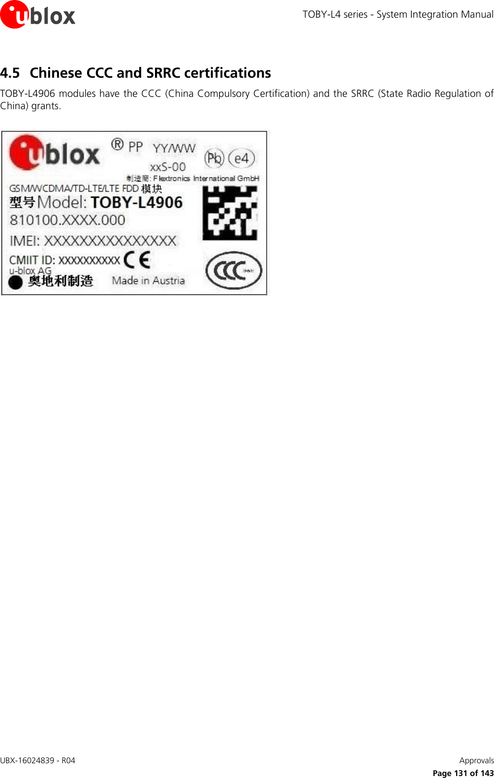
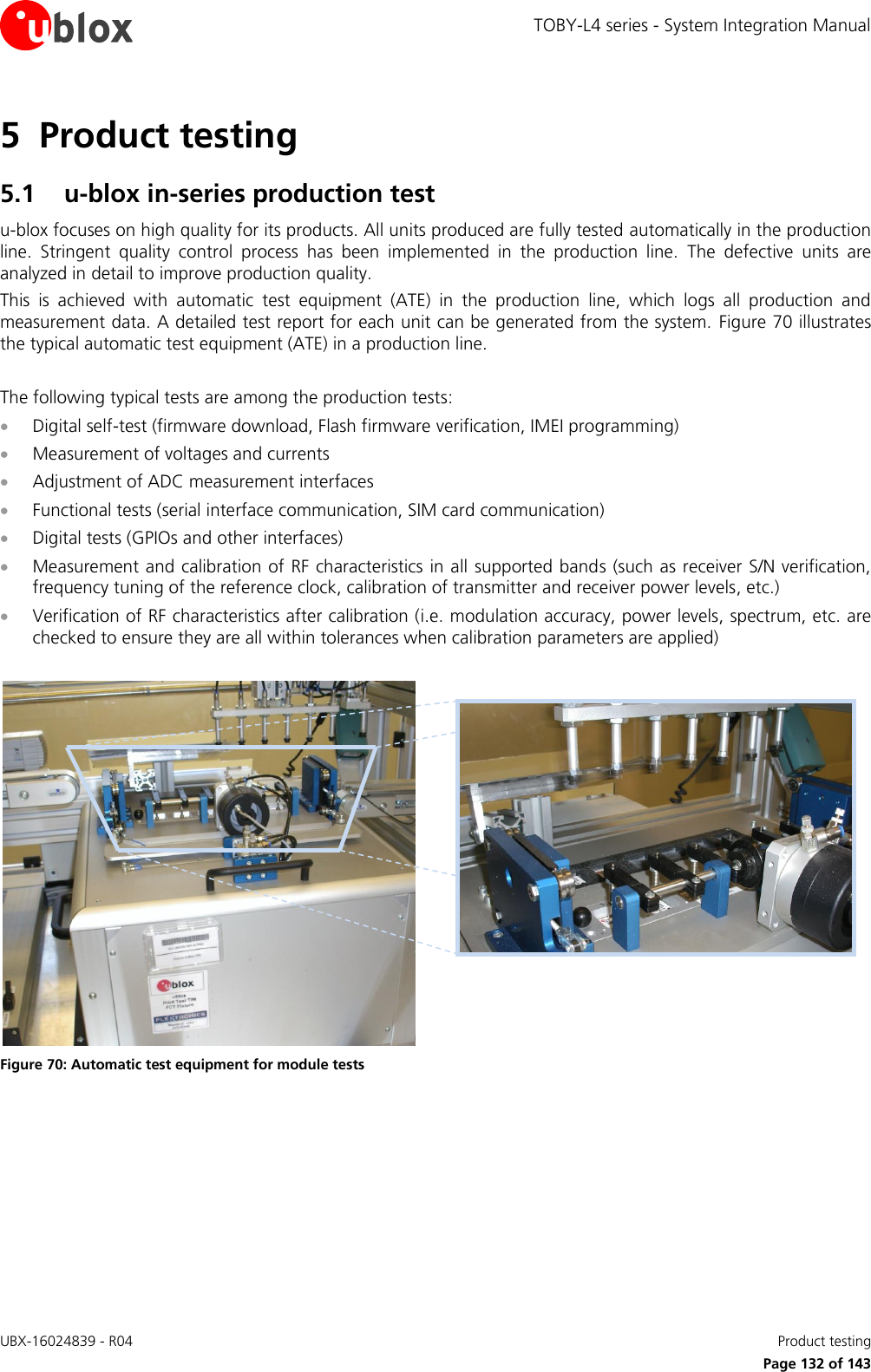
![TOBY-L4 series - System Integration Manual UBX-16024839 - R04 Product testing Page 133 of 143 5.2 Test parameters for OEM manufacturers Because of the testing performed by u-blox (with 100% coverage), an OEM manufacturer does not need to repeat firmware tests or measurements of the module RF performance or tests over analog and digital interfaces in their production test. However, an OEM manufacturer should focus on: Module assembly on the device; it should be verified that: o Soldering and handling processes did not damage the module components o All module pins are well soldered on the device board o There are no short circuits between pins Component assembly on the device; it should be verified that: o Communications with the external host controller can be established o The interfaces between the module and external devices are working o Overall RF performance test of the device including the antenna Dedicated tests can be implemented to check the device. For example, the measurement of module current consumption when set in a specified status can detect a short circuit if compared with a “Golden Device” result. In addition, module AT commands can be used to perform functional tests on digital interfaces (communication with host controller, check SIM interface, GPIOs, etc.), on audio interfaces (audio loop for test purposes can be enabled as described in the u-blox AT Commands Manual [2]), and to perform RF performance tests (see the following section 5.2.2 for details). 5.2.1 “Go/No go” tests for integrated devices A “Go/No go” test is typically performed to compare the signal quality with a “Golden Device” in a location with excellent network coverage and known signal quality. This test should be performed after data connection has been established. AT+CSQ is the typical AT command used to check signal quality in term of RSSI. See the u-blox AT Commands Manual [2] for details of the AT command. These kinds of test may be useful as a “go/no go” test but not for RF performance measurements. This test is suitable to check the functionality of communication with the host controller or SIM card as well as the power supply. It is also a means to verify if the components are well soldered at the antenna interface. 5.2.2 RF functional tests The overall RF functional test of the OEM device integrating the cellular module, including the antenna(s), can be performed in the OEM production line with basic instruments such as a spectrum analyzer (or an RF power meter) and a signal generator with the assistance of the AT+UTEST command over the AT command user interface. The AT+UTEST command provides a simple interface to set the module to Rx or Tx test modes ignoring the LTE/3G/2G signaling protocol. The command can set the module into: transmitting mode in a specified channel and power level in all supported modulation schemes and bands receiving mode in a specified channel to returns the measured power level in all supported bands See the u-blox AT Commands Manual [2] for the AT+UTEST command syntax description.](https://usermanual.wiki/u-blox/1EHQ37NN.TempConfidential-TOBY-L4-SysIntegrManual-UBX-16024839/User-Guide-3759877-Page-133.png)
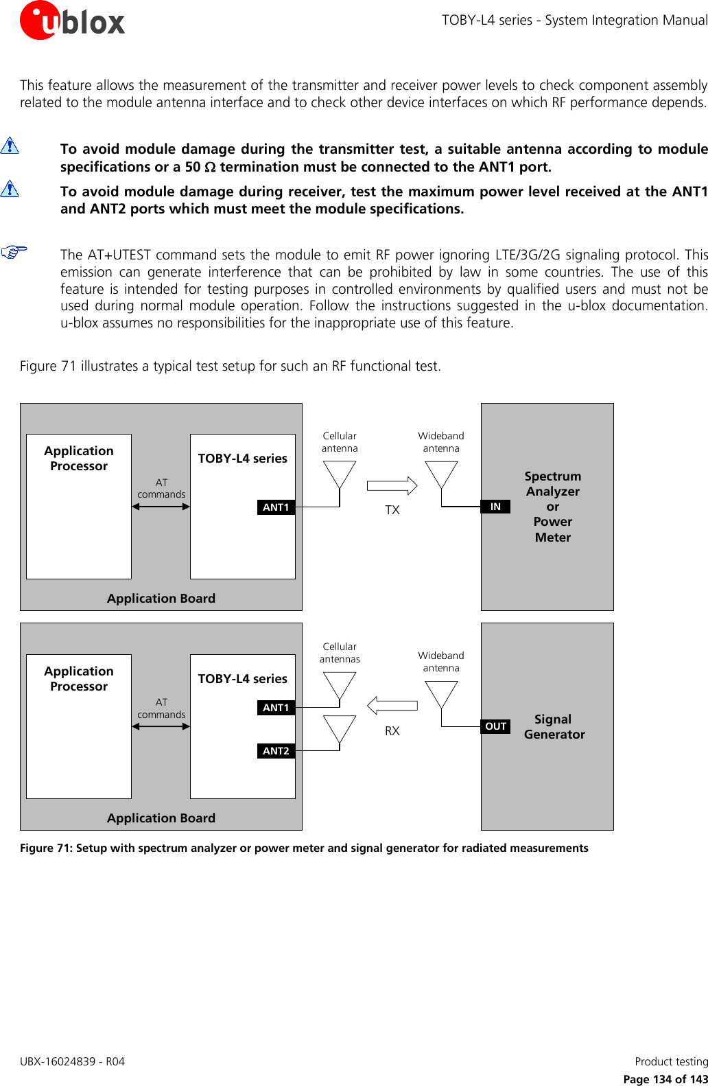
![TOBY-L4 series - System Integration Manual UBX-16024839 - R04 Appendix Page 135 of 143 Appendix A Migration between TOBY-L2 and TOBY-L4 A.1 Overview TOBY-L2 and TOBY-L4 series cellular modules have the same TOBY form factor (35.6 x 24.8 mm LGA), with a different number of pins: as illustrated in Figure 72, TOBY-L2 modules have 152 pins, while TOBY-L4 modules have the same 152 pins of TOBY-L2 modules plus 96 additional pins, reaching a total number of 248 pins. Figure 72 shows that all the functions provided by the 152 pins of TOBY-L2 modules are also available on the same pins of TOBY-L4 modules, which provide additional functions (RGMII and UART3 interfaces) on RSVD pins of TOBY-L2 modules, intended to be left unconnected on a board designed for TOBY-L2 modules. This means that TOBY-L2 and TOBY-L4 series modules can be alternatively mounted on a single application board using exactly the same copper mask, solder mask and paste mask: TOBY-L4 series modules can be mounted on any design appropriately implemented for TOBY-L2 modules, given that any additional interface provided by TOBY-L4 modules will result not connected. SDIO_CMDSDIO_D0GNDVCCVCCGNDANT_DETSDASIM_IOSIM_RSTGPIO5GPIO6SDIO_D2SDIO_CLKRSVDRSVDI2S_WAI2S_CLKI2S_RXDSDIO_D1VCCGNDSCLSIM_CLKVSIMHOST_SELECT1RSVDI2S_TXDSDIO_D3V_INTVUSB_DETGNDRSVDGPIO1RSVDRSVDTXDRSVDUSB_D-HOST_SELECT0GPIO3RESET_NV_BCKPGPIO2PWR_ONRXDUSB_D+GPIO4GNDRSVDGNDGNDRSVDGNDGNDGNDGNDGNDGNDGNDGNDGNDRSVDANT2ANT1GNDRSVDGNDGNDRSVDGNDRSVDRSVDRSVDRSVDRSVDRSVDRSVDRSVDRSVDRSVDRSVDRIDSRRSVDCTSDTRDCDRSVDRSVDRTSRSVD11107542121191816151312292726242386322201714282596566697172747555575860616364474950525368707354565962485167909192 78 77 7693 10079808385868889 828487 81323130 44 45 46145 15243423937363433 403835 41999897969594106105104103102101108107124123130129128127126125136135134133132131138137144143142141140139151150149148147146114113112111110109120119118117116115122121TOBY-L2Pin 93-152: GNDSDIO_CMDSDIO_D0GNDVCCVCCGNDANT_DETSDASIM_IOSIM_RSTGPIO5GPIO6SDIO_D2SDIO_CLKRSVDRSVDI2S_WAI2S_CLKI2S_RXDSDIO_D1VCCGNDSCLSIM_CLKVSIMHOST_SELECT1RSVDI2S_TXDSDIO_D3V_INTVUSB_DETGNDRSVDGPIO1RXD3TXD3TXDETH_TX_CLKUSB_D-HOST_SELECT0GPIO3RESET_NV_BCKPGPIO2PWR_ONRXDUSB_D+GPIO4GNDRSVDGNDGNDRSVDGNDGNDGNDGNDGNDGNDGNDGNDGNDRSVDANT2ANT1GNDRSVDGNDGNDRSVDGNDETH_RX_CLKETH_RX_CTLETH_RXD1ETH_TXD0ETH_TXD1ETH_TXD3ETH_TX_CTLETH_RXD2ETH_RXD0ETH_TXD2ETH_RXD3RIDSRRSVDCTSDTRDCDRSVDRSVDRTSRSVD11RI10DSR7RSVD5V_INT4VUSB_D ET2GND1RSVD21GPIO119RSVD18RSVD16TXD15CTS13DTR12DCD29ETH_ TX_CLK27USB_D –26HOST_ SELECT024GPIO323RESET_N8RSVD6RSVD3V_BCKP22GPIO220PWR_ON17RXD14RTS28USB_D +25GPIO49RSVD65SDIO_C MD66SDIO_D 069GND71VCC72VCC74GND75ANT_D ET55SDA57SIM_IO58SIM_R ST60GPIO561GPIO663SDIO_D 264SDIO_C LK47RSVD49RSVD50I2S_WA52I2S_CL K53I2S_RXD68SDIO_D 170VCC73GND54SCL56SIM_C LK59VSIM62HOST_ SELECT148RSVD51I2S_TXD67SDIO_D 390GND91RSVD92GND78GND 77RSVD76GND93GND100GND79GND80GND83GND85GND86GND88GND89GND82GND84RSVD87ANT281ANT132GND31RSVD30GND44GND45RSVD 46GND145GND152GND43ETH_RX_CL K42ETH_RX_CTL39ETH_RXD137ETH_TXD036ETH_TXD134ETH_TXD333ETH_TX_CTL40ETH_RXD238ETH_RXD035ETH_TXD241ETH_RXD399GND98GND97GND96GND95GND94GND106GND105GND104GND103GND102GND101GND108GND107GND124GND123GND130GND129GND128GND127GND126GND125GND136GND135GND134GND133GND132GND131GND138GND137GND144GND143GND142GND141GND140GND139GND151GND150GND149GND148GND147GND146GND114GND113GND112GND111GND110GND109GND120GND119GND118GND117GND116GND115GND122GND121GNDTOBY-L4155RSVD153RSVD157RSVD156RSVD154RSVD158RSVD195CTS1193RTS1197RSVD196RSVD194RSVD198RSVD207I2S1_RXD206I2S1_TXD203SCL1201RSVD200RSVD217MMC_D2215MMC_CMD214MMC_D0212MMC_D1211MMC_ RST_N209GND208I2S1_CL K222ETH_ MDIO220ETH_ INTR219GND204SDA1202RSVD199RSVD218MMC_CD_N216MMC_CLK213MMC_D3210V_MMC221V_ETH205I2S1_WA223ETH_ MDC240ADC1241GND244RSVD246RSVD247GPIO8230MIC_GND232GND233MIC2_ N235GND236MIC1_ N238GND239ADC2225RSVD227SPK_P228SPK_N243RSVD245RSVD248GPIO7229GND231MIC_ BIAS234MIC2_ P237MIC1_ P226GND242RSVD224RSVD162RXD2161TXD2160RXD1159TXD1168USB_I D163RSVD167RSVD166RSVD165RSVD164RSVD172VSIM1171USB_SSR X–170USB_SSR X+169SPI_MISO182SIM1_C LK181RSVD180RSVD179SPI_SCL K178SIM1_IO173SPI_CS177SIM1_R ST176USB_SSTX–175USB_SSTX+174SPI_MOSI188RSVD183RSVD187RSVD186RSVD185RSVD184RSVD192RSVD191RSVD190RSVD189RSVDPin 93-152: GND Figure 72: TOBY-L2 and TOBY-L4 series modules pad layout and pin assignment TOBY modules are also form-factor compatible with the u-blox LISA, SARA and LARA cellular module families: although TOBY modules, LISA modules (33.2 x 22.4 mm, 76-pin LCC), SARA modules (26.0 x 16.0 mm, 96-pin LGA) and LARA modules (26.0 x 24.0 mm, 100-pin LGA) each have different form factors, the footprints for the TOBY, LISA, SARA and LARA modules have been developed to ensure layout compatibility. With the u-blox “nested design” solution, any TOBY, LISA, SARA or LARA module can be alternatively mounted on the same space of a single “nested” application board as described in the Nested Design Application Note [19].](https://usermanual.wiki/u-blox/1EHQ37NN.TempConfidential-TOBY-L4-SysIntegrManual-UBX-16024839/User-Guide-3759877-Page-135.png)
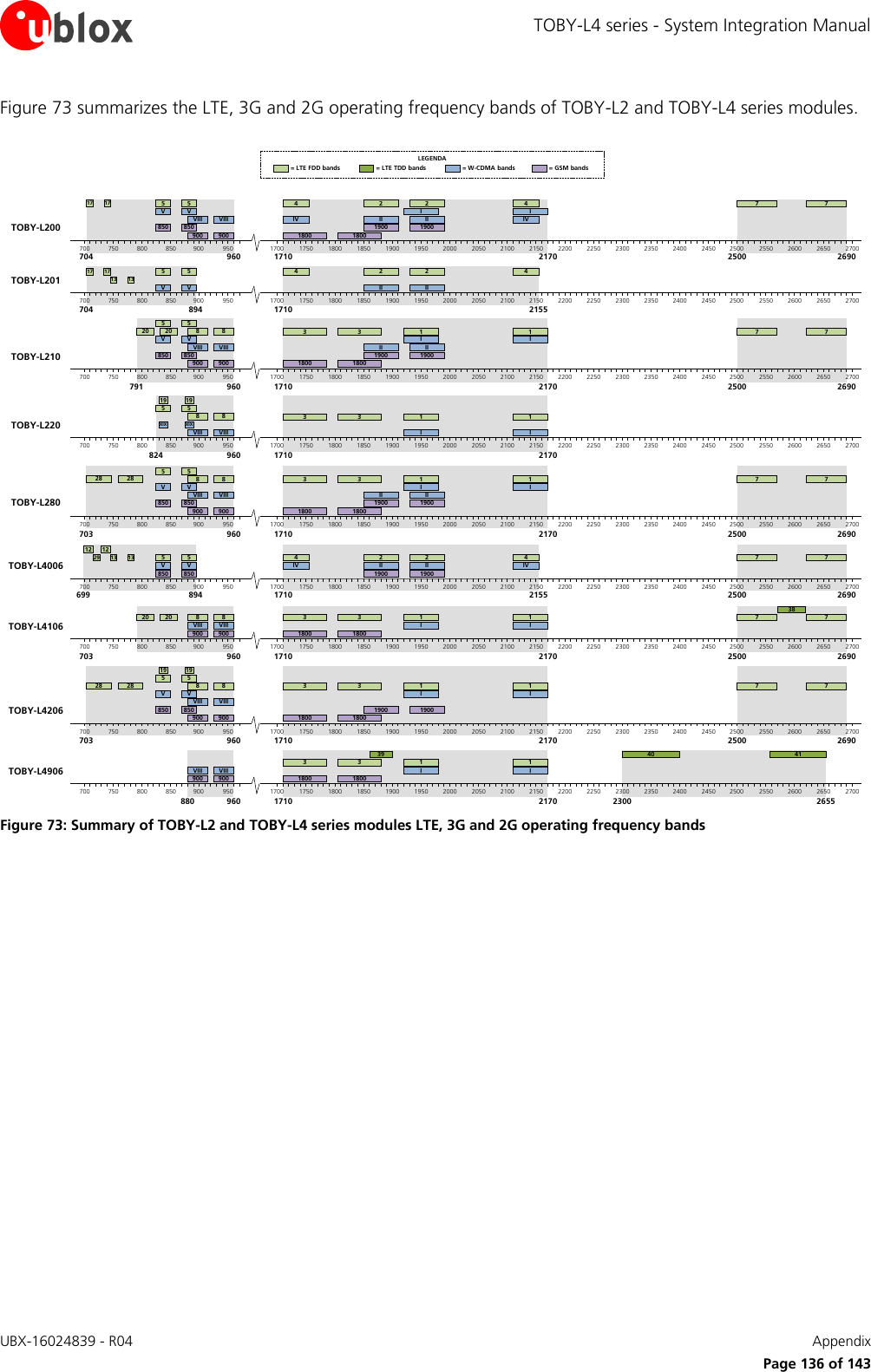
![TOBY-L4 series - System Integration Manual UBX-16024839 - R04 Appendix Page 137 of 143 A.2 Pin-out comparison between TOBY-L2 and TOBY-L4 TOBY-L2 TOBY-L4 Pin No Pin Name Description Pin Name Description Remarks for migration 1 RSVD Reserved RSVD Reserved 2 GND Ground GND Ground 3 V_BCKP RTC Back-up Supply V_BCKP RTC Back-up Supply 4 VUSB_DET Not supported VUSB_DET VBUS USB supply (5 V) detection 5 V must be applied at VUSB_DET of TOBY-L4 to enable USB device. The pin must be left unconnected on TOBY-L2, as it is not supported. 5 V_INT 1.8 V Interfaces Supply Output V_INT 1.8 V Interfaces Supply Output 6 RSVD Reserved This pin must be connected to GND RSVD Reserved This pin must be connected to GND 7-9 RSVD Reserved RSVD Reserved 10 DSR UART DSR Output22 / GPIO23 DSR GPIO24 / EINT24 11 RI UART RI Output22 / GPIO23 RI UART0 RI Output / GPIO / EINT24 12 DCD UART DCD Output22 / GPIO23 DCD GPIO24 / EINT24 13 DTR UART DTR Input22 / GPIO23 DTR GPIO24 / EINT24 14 RTS UART RTS Input22 RTS UART0 RTS Input24 15 CTS UART CTS Output22 CTS UART0 CTS Output24 16 TXD UART Data Input22 TXD UART0 Data Input24 17 RXD UART Data Output22 RXD UART0 Data Output24 18 RSVD Reserved TXD3 UART3 Data Input24 RSVD UART3 19 RSVD Reserved RXD3 UART3 Data Output24 RSVD UART3 20 PWR_ON Power-on Input Internal 50k pull-up to VCC Switch-on, Switch-off PWR_ON Power-on Input Internal 35k pull-up to 1.3 V Switch-on, Switch-off Internal pull-up slightly different No functional difference 21 GPIO1 GPIO23 GPIO1 GPIO 22 GPIO2 GPIO23 GPIO2 GPIO 23 RESET_N Reset signal Input Internal 50k pull-up to VCC Reset, Switch-on, Switch-off RESET_N Reset signal Input Internal 100k pull-up to V_INT Reset Internal pull-up slightly different. Function slightly different. 24 GPIO3 GPIO23 GPIO3 GPIO 25 GPIO4 GPIO23 GPIO4 GPIO 26 HOST_SELECT0 Not supported HOST_SELECT0 GPIO24 / EINT24 Not supported GPIO / EINT 27 USB_D- USB Data I/O (D-) USB_D- USB Data I/O (D-) 28 USB_D+ USB Data I/O (D+) USB_D+ USB Data I/O (D+) 29 RSVD Reserved ETH_TX_CLK Ethernet Transmission Clock24 RSVD RGMII 30 GND Ground GND Ground 31 RSVD Reserved RSVD Reserved 32 GND Ground GND Ground 33 RSVD Reserved ETH_TX_CTL Ethernet Transmit Control24 RSVD RGMII 34 RSVD Reserved ETH_TXD3 Ethernet Transmit Data [3]24 RSVD RGMII 35 RSVD Reserved ETH_TXD2 Ethernet Transmit Data [2]24 RSVD RGMII 36 RSVD Reserved ETH_TXD1 Ethernet Transmit Data [1]24 RSVD RGMII 37 RSVD Reserved ETH_TXD0 Ethernet Transmit Data [0]24 RSVD RGMII 38 RSVD Reserved ETH_RXD0 Ethernet Receive Data [0]24 RSVD RGMII 39 RSVD Reserved ETH_RXD1 Ethernet Receive Data [1]24 RSVD RGMII 40 RSVD Reserved ETH_RXD2 Ethernet Receive Data [2]24 RSVD RGMII 41 RSVD Reserved ETH_RXD3 Ethernet Receive Data [3]24 RSVD RGMII 42 RSVD Reserved ETH_RX_CTL Ethernet Receive Control24 RSVD RGMII 43 RSVD Reserved ETH_RX_CLK Ethernet Receive Clock24 RSVD RGMII 44 GND Ground GND Ground 45 RSVD Reserved RSVD Reserved 46 GND Ground GND Ground 22 Not supported by "00" product versions 23 Not supported by "00", "01", "60" product versions 24 Not supported by "50" product versions](https://usermanual.wiki/u-blox/1EHQ37NN.TempConfidential-TOBY-L4-SysIntegrManual-UBX-16024839/User-Guide-3759877-Page-137.png)
![TOBY-L4 series - System Integration Manual UBX-16024839 - R04 Appendix Page 138 of 143 TOBY-L2 TOBY-L4 Pin No Pin Name Description Pin Name Description Remarks for migration 47-49 RSVD Reserved RSVD Reserved 50 I2S_WA I2S Word Alignment22 / GPIO23 I2S_WA I2S Word Alignment I2S / GPIO I2S 51 I2S_TXD I2S Data Output22 / GPIO23 I2S_TXD I2S Data Output I2S / GPIO I2S 52 I2S_CLK I2S Clock22 / GPIO23 I2S_CLK I2S Clock I2S / GPIO I2S 53 I2S_RXD I2S Data Input22 / GPIO23 I2S_RXD I2S Data Input I2S / GPIO I2S 54 SCL I2C Clock Output25 SCL I2C Clock Output26 55 SDA I2C Data I/O25 SDA I2C Data I/O26 56 SIM_CLK SIM Clock Output SIM_CLK SIM Clock Output 57 SIM_IO SIM Data I/O SIM_IO SIM Data I/O 58 SIM_RST SIM Reset Output SIM_RST SIM Reset Output 59 VSIM SIM Supply Output VSIM SIM Supply Output 60 GPIO5 GPIO25 GPIO5 GPIO 61 GPIO6 GPIO25 GPIO6 GPIO 62 HOST_SELECT1 Not supported HOST_SELECT1 GPIO26 / EINT26 Not supported GPIO / EINT 63 SDIO_D2 SDIO serial data [2]25 SDIO_D2 SDIO serial data [2]26 64 SDIO_CLK SDIO serial clock25 SDIO_CLK SDIO serial clock26 65 SDIO_CMD SDIO command25 SDIO_CMD SDIO command26 66 SDIO_D0 SDIO serial data [0]25 SDIO_D0 SDIO serial data [0]26 67 SDIO_D3 SDIO serial data [3]25 SDIO_D3 SDIO serial data [3]26 68 SDIO_D1 SDIO serial data [1]25 SDIO_D1 SDIO serial data [1]26 69 GND Ground GND Ground 70-72 VCC Module Supply Input 3.40 V – 4.35 V normal range 3.20 V – 4.35 V extended range VCC Module Supply Input 3.40 V – 4.40 V normal range 3.00 V – 4.50 V extended range Larger operating ranges on TOBY-L4 73-74 GND Ground GND Ground 75 ANT_DET Antenna Detection Input25 ANT_DET Antenna Detection Input 76 GND Ground GND Ground 77 RSVD Reserved RSVD Reserved 78-80 GND Ground GND Ground 81 ANT1 RF Antenna Input/Output Up to six LTE bands Up to five 3G bands Up to four 2G bands ANT1 RF Antenna Input/Output Up to seven LTE bands Up to three 3G bands Up to four 2G bands No RF functional difference Different operating bands (Figure 73) 82-83 GND Ground GND Ground 84 RSVD Reserved RSVD Reserved 85-86 GND Ground GND Ground 87 ANT2 RF Antenna Input ANT2 RF Antenna Input No RF functional difference Different operating bands (Figure 73) 88-90 GND Ground GND Ground 91 RSVD Reserved RSVD Reserved 92-152 GND Ground GND Ground 152-248 Pins not available Additional functions Not available Additional functions Table 52: TOBY-L2 and TOBY-L4 series modules pin assignment with remarks for migration For further details regarding the characteristics, capabilities, usage or settings applicable for each interface of the cellular modules, see the TOBY-L4 series Data Sheet [1], the TOBY-L2 series Data Sheet [17], the TOBY-L2 / MPCI-L2 series System Integration Manual [18], and the u-blox AT Commands Manual [2]. 25 Not supported by "00", "01", "60" product versions 26 Not supported by "50" product versions](https://usermanual.wiki/u-blox/1EHQ37NN.TempConfidential-TOBY-L4-SysIntegrManual-UBX-16024839/User-Guide-3759877-Page-138.png)
![TOBY-L4 series - System Integration Manual UBX-16024839 - R04 Related documents Page 141 of 143 Related documents [1] u-blox TOBY-L4 series Data Sheet, Docu No UBX-16009856 [2] u-blox AT Commands Manual, Docu No UBX-13002752 [3] Universal Serial Bus Rev. 2.0 specification, http://www.usb.org/developers/docs/usb20_docs/ [4] Universal Serial Bus Rev. 3.0 specification, http://www.usb.org/developers/docs/documents_archive/ [5] ITU-T Recommendation V.24 - 02-2000 - List of definitions for interchange circuits between Data Terminal Equipment (DTE) and Data Circuit-terminating Equipment (DCE), http://www.itu.int/rec/T-REC-V.24-200002-I/en [6] I2C-bus specification and user manual - Rev. 5 - 9 October 2012 - NXP Semiconductors, http://www.nxp.com/documents/user_manual/UM10204.pdf [7] Reduced Gigabit Media-Independent Interface (RGMII) Version 1.3, www.hp.com/rnd/pdfs/RGMIIv1_3.pdf [8] Reduced Media-Independent Interface (RMII) Specification, Rev. 1.2 [9] JESD84-B451 - Embedded Multimedia Card (eMMC), Electrical Standard 4.51 [10] GSM Association TS.09 - Battery Life Measurement and Current Consumption Technique https://www.gsma.com/newsroom/wp-content/uploads//TS.09_v10.0.pdf [11] 3GPP TS 51.010-2 - Technical Specification Group GSM/EDGE Radio Access Network; Mobile Station (MS) conformance specification; Part 2: Protocol Implementation Conformance Statement (PICS) [12] 3GPP TS 34.121-2 - Technical Specification Group Radio Access Network; User Equipment (UE) conformance specification; Radio transmission and reception (FDD); Part 2: Implementation Conformance Statement (ICS) [13] 3GPP TS 36.521-1 - Evolved Universal Terrestrial Radio Access; User Equipment conformance specification; Radio transmission and reception; Part 1: Conformance Testing [14] 3GPP TS 36.521-2 - Evolved Universal Terrestrial Radio Access (E-UTRA); User Equipment conformance specification; Radio transmission and reception; Part 2: Implementation Conformance Statement (ICS) [15] 3GPP TS 36.523-2 - Evolved Universal Terrestrial Radio Access (E-UTRA) and Evolved Packet Core (EPC); User Equipment conformance specification; Part 2: Implementation Conformance Statement (ICS) [16] u-blox Package Information Guide, Docu No UBX-14001652 [17] u-blox TOBY-L2 series Data Sheet, Docu No UBX-13004573 [18] u-blox TOBY-L2 / MPCI-L2 series System Integration Manual, Docu No UBX- 13004618 [19] u-blox Nested Design Application Note, Docu No UBX-16007243 Some of the above documents can be downloaded from the u-blox web-site (http://www.u-blox.com/).](https://usermanual.wiki/u-blox/1EHQ37NN.TempConfidential-TOBY-L4-SysIntegrManual-UBX-16024839/User-Guide-3759877-Page-141.png)