u blox 2AGQN1NNN LTE Cat-M1 Module User Manual SARA R4 series System Integration Manual
u-blox AG LTE Cat-M1 Module SARA R4 series System Integration Manual
UserManual.wiki
>
u blox
>
2AGQN1NNN User Manual
User Manual
Navigation menu
Upload a User Manual
Namespaces
Wiki Guide
HTML
PDF
Info
Views
User Manual
Discussion / Help
Navigation
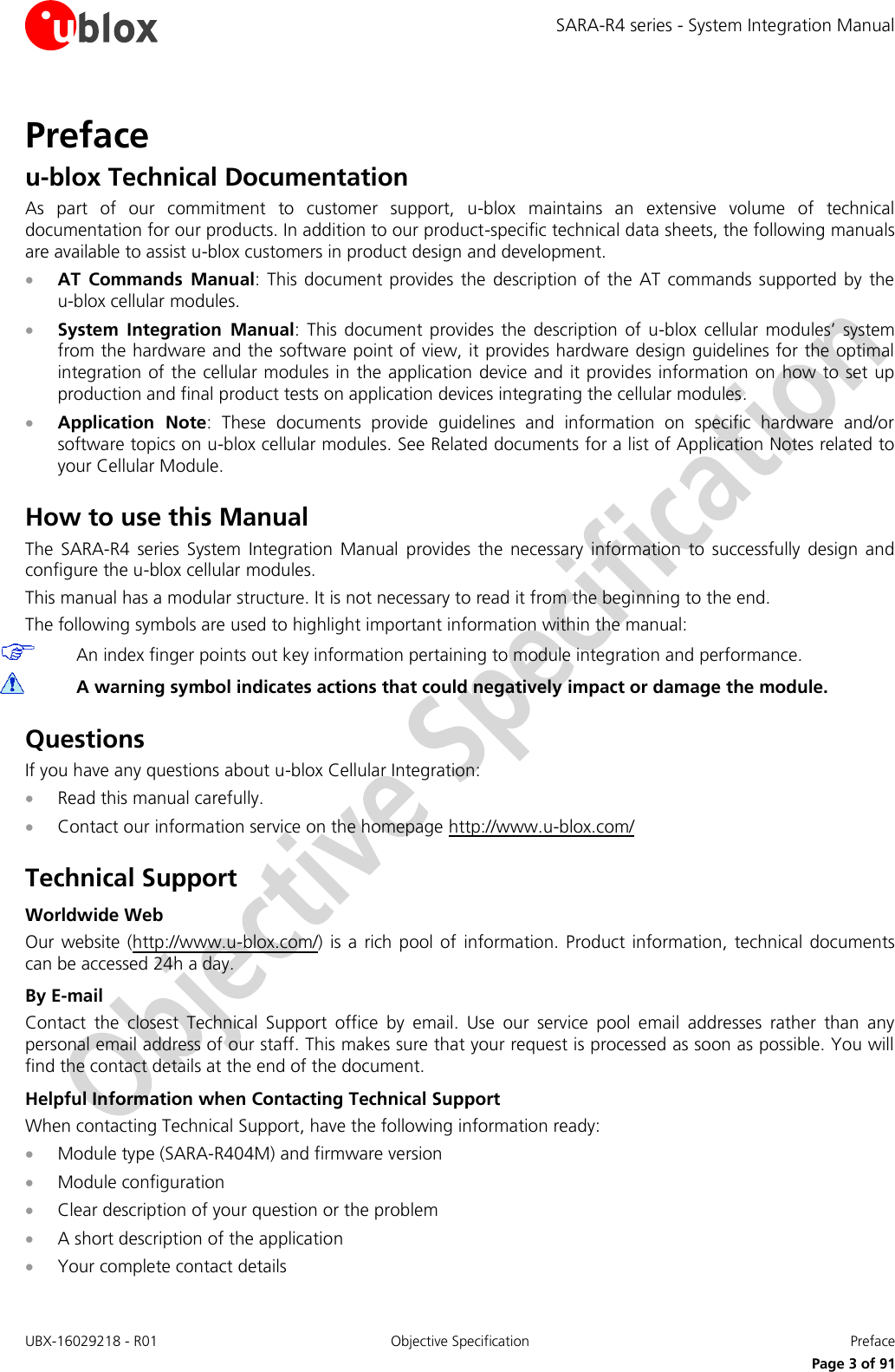
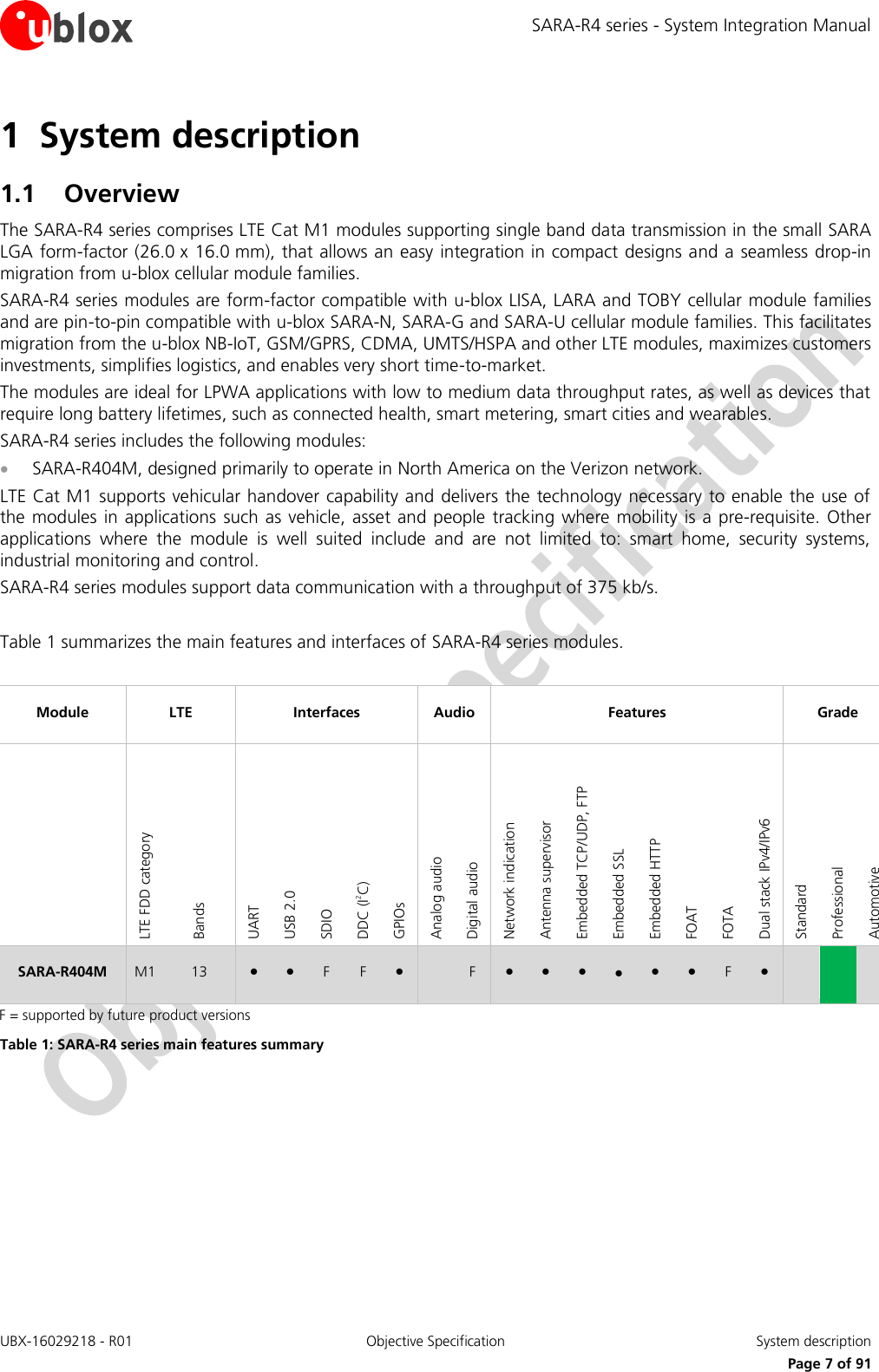
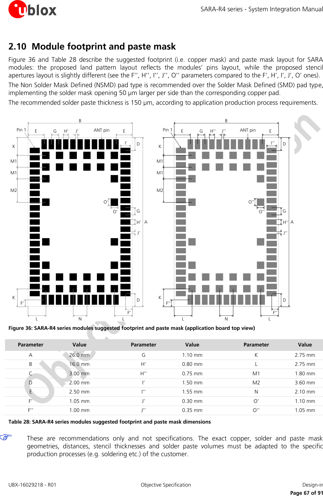
![SARA-R4 series - System Integration Manual UBX-16029218 - R01 Objective Specification System description Page 11 of 91 Function Pin Name Pin No I/O Description Remarks USB VUSB_DET 17 I USB detect input VBUS (5 V typical) USB supply generated by the host must be connected to this input pin to enable the USB interface. If the USB interface is not used by the Application Processor, Test-Point for diagnostic / FW update access is recommended See section 1.9.2 for functional description. See section 2.6.2 for external circuit design-in. USB_D- 28 I/O USB Data Line D- USB interface for AT commands, data communication, FOAT, FW update by u-blox EasyFlash tool and diagnostic. 90 nominal differential impedance (Z0) 30 nominal common mode impedance (ZCM) Pull-up or pull-down resistors and external series resistors as required by the USB 2.0 specifications [4] are part of the USB pin driver and need not be provided externally. If the USB interface is not used by the Application Processor, Test-Point for diagnostic / FW update access is recommended. See section 1.9.2 for functional description. See section 2.6.2 for external circuit design-in. USB_D+ 29 I/O USB Data Line D+ USB interface for AT commands, data communication, FOAT, FW update by u-blox EasyFlash tool and diagnostic. 90 nominal differential impedance (Z0) 30 nominal common mode impedance (ZCM) Pull-up or pull-down resistors and external series resistors as required by the USB 2.0 specifications [4] are part of the USB pin driver and need not be provided externally. If the USB interface is not used by the Application Processor, Test-Point for diagnostic / FW update access is recommended. See section 1.9.2 for functional description. See section 2.6.2 for external circuit design-in. DDC SCL 27 O I2C bus clock line 1.8 V open drain, for communication with I2C-slave devices. External pull-up are not required. See section 1.9.3 for functional description. See section 2.6.3 for external circuit design-in. SDA 26 I/O I2C bus data line 1.8 V open drain, for communication with I2C-slave devices. External pull-up are not required. See section 1.9.3 for functional description. See section 2.6.3 for external circuit design-in. GPIO GPIO1 16 I/O GPIO 1.8 V GPIO with alternatively configurable functions. See section 1.10 for functional description. See section 2.7 for external circuit design-in. GPIO2 23 I/O GPIO 1.8 V GPIO with alternatively configurable functions. See section 1.10 for functional description. See section 2.7 for external circuit design-in. GPIO3 24 I/O GPIO 1.8 V GPIO with alternatively configurable functions. See section 1.10 for functional description. See section 2.7 for external circuit design-in. GPIO4 25 I/O GPIO 1.8 V GPIO with alternatively configurable functions. See section 1.10 for functional description. See section 2.7 for external circuit design-in. SIM_DET 42 I/O GPIO 1.8 V GPIO with alternatively configurable functions. See section 1.10 for functional description. See section 2.7 for external circuit design-in. Reserved RSVD 2, 31, 33-37, 44-49 N/A Reserved pin Leave unconnected. See sections 1.11 and 2.8 Table 3: SARA-R4 series module pin definition, grouped by function](https://usermanual.wiki/u-blox/2AGQN1NNN/User-Guide-3327358-Page-11.png)
![SARA-R4 series - System Integration Manual UBX-16029218 - R01 Objective Specification System description Page 12 of 91 1.4 Operating modes SARA-R4 series modules have several operating modes. The operating modes are defined in Table 4 and described in detail in Table 5, providing general guidelines for operation. General Status Operating Mode Definition Power-down Not-Powered Mode VCC supply not present or below operating range: module is switched off. Power-Off Mode VCC supply within operating range and module is switched off. Normal Operation Idle-Mode Module processor core runs with 32 kHz reference internally generated. Active-Mode Module processor core runs with 19.2 MHz reference generated by the internal oscillator. Connected-Mode RF Tx/Rx data connection enabled and processor core runs with 19.2 MHz reference. Table 4: SARA-R4 series modules operating modes definition Mode Description Transition between operating modes Not-Powered Module is switched off. Application interfaces are not accessible. When VCC supply is removed, the modules enter not-powered mode. When in not-powered mode, the module can enter power-off mode applying VCC supply (see 1.6.1). Power-Off Module is switched off: normal shutdown by an appropriate power-off event (see 1.6.2). Application interfaces are not accessible. When the modules are switched off by an appropriate switch-off event (see 1.6.2), the modules enter power-off mode from active-mode. When in power-off mode, the modules can be switched on by PWR_ON. When in power-off mode, the modules enter not-powered mode by removing VCC supply. Idle Module is switched on with application interfaces temporarily disabled or suspended: the module is temporarily not ready to communicate with an external device by means of the application interfaces as configured to reduce the current consumption. The module enters the low power idle-mode whenever possible if power saving is enabled by AT+UPSV command (see u-blox SARA-R404M AT Commands Manual [1]) reducing current consumption (see 1.5.1.3). The CTS output line indicates when the UART interface is disabled/enabled due to the module idle/active-mode transitions according to the power saving and HW flow control settings (see 1.9.1.2). Power saving configuration is not enabled by default; it can be enabled by AT+UPSV (see the u-blox SARA-R404M AT Commands Manual [1]). The modules automatically switch from the active-mode to low power idle-mode whenever possible if power saving is enabled (see sections 1.5.1.30 and u-blox SARA-R404M AT Commands Manual [1], AT+UPSV command). The modules wake up from low power idle-mode to active-mode in the following events: Automatic periodic monitoring of the paging channel for the paging block reception according to network conditions (see 1.5.1.3) Automatic periodic enable of the UART interface to receive / send data, with AT+UPSV=1 Data received over UART, according to HW flow control (AT&K) and power saving (AT+UPSV) settings RTS input set ON by the host DTE, with HW flow control disabled and AT+UPSV=2 DTR input set ON by the host DTE, with AT+UPSV=3 USB detection, applying 5 V (typ.) to VUSB_DET input (see 1.9.2) The connected USB host forces a remote wakeup of the module as USB device (see 0) Active Module is switched on with application interfaces enabled or not suspended: the module is ready to communicate with an external device by means of the application interfaces unless power saving configuration is enabled by AT+UPSV (see 0u-blox SARA-R404M AT Commands Manual [1]). When the modules are switched on by an appropriate power-on event (see 1.6.1), the modules enter active-mode from not-powered or power-off mode. If power saving configuration is enabled by the AT+UPSV command, the module automatically switches from active to idle-mode whenever possible and the module wakes up from idle to active-mode in the events listed above (see idle-mode to active-mode transition description above). When a RF Tx/Rx data connection is initiated or when RF Tx/Rx activity is required due to a connection previously initiated, the module switches from active to connected-mode.](https://usermanual.wiki/u-blox/2AGQN1NNN/User-Guide-3327358-Page-12.png)
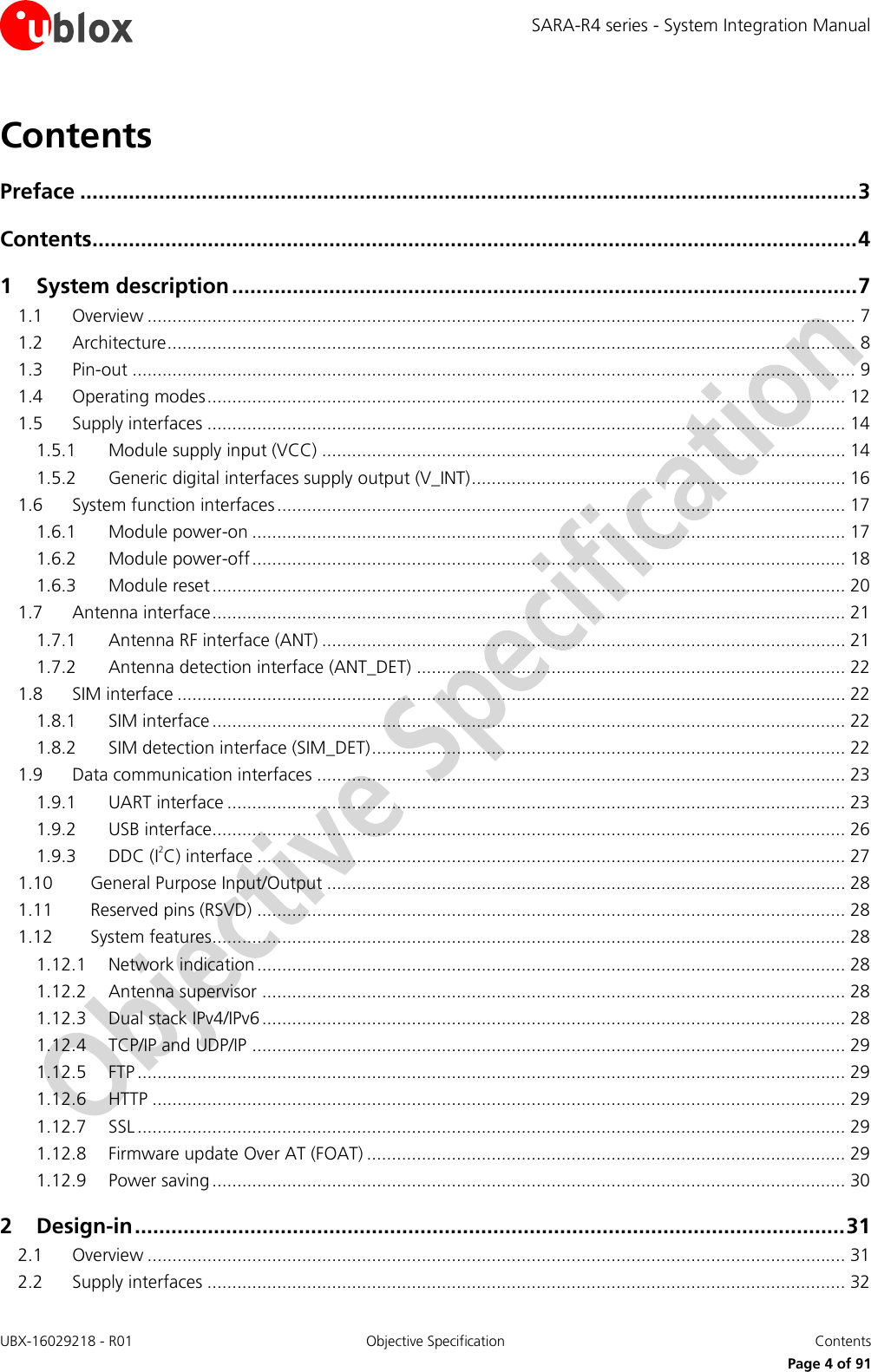
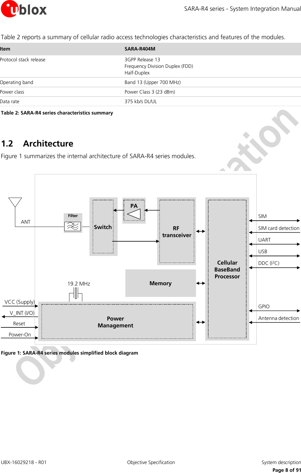
![SARA-R4 series - System Integration Manual UBX-16029218 - R01 Objective Specification System description Page 13 of 91 Mode Description Transition between operating modes Connected RF Tx/Rx data connection is in progress. The module is prepared to accept data signals from an external device unless power saving configuration is enabled by AT+UPSV (see 0u-blox SARA-R404M AT Commands Manual [1]). When a data connection is initiated, the module enters connected-mode from active-mode. Connected-mode is suspended if Tx/Rx data is not in progress, due to connected discontinuous reception and fast dormancy capabilities of the module and according to the network environment settings and scenario. In such cases the module automatically switches from connected to active mode and then, if power saving configuration is enabled by the AT+UPSV command, the module automatically switches to idle-mode whenever possible. Vice-versa, the module wakes up from idle to active mode and then connected mode if RF Tx/Rx activity is necessary. When a data connection is terminated, the module returns to the active-mode. Table 5: SARA-R4 series modules operating modes description Figure 2 describes the transition between the different operating modes. If power saving is enabled and there is no activity for a defined time intervalAny wake up event described in the module operating modes summary table aboveIncoming/outgoing data or other dedicated device network communicationNo RF Tx/Rx in progress, Communication droppedRemove VCCSwitch ON:•PWR_ONNot poweredPower offActiveConnected IdleSwitch OFF:•AT+CPWROFFApply VCC Figure 2: SARA-R4 series modules operating modes transitions](https://usermanual.wiki/u-blox/2AGQN1NNN/User-Guide-3327358-Page-13.png)
![SARA-R4 series - System Integration Manual UBX-16029218 - R01 Objective Specification System description Page 14 of 91 1.5 Supply interfaces 1.5.1 Module supply input (VCC) The modules must be supplied via the three VCC pins that represent the module power supply input. During operation, the current drawn by the SARA-R4 series modules through the VCC pins can vary by several orders of magnitude, depending on the operating mode and state (as described in sections 1.5.1.2, 1.5.1.3 and 1.5.1.4). It is important that the supply source is able to support the average current consumption occurring during a LTE transmission at maximum RF power level. 1.5.1.1 VCC supply requirements Table 6 summarizes the requirements for the VCC modules supply. See section 2.2.1 for suggestions to properly design a VCC supply circuit compliant with the requirements listed in Table 6. The supply circuit affects the RF compliance of the device integrating SARA-R4 series modules with applicable required certification schemes as well as antenna circuit design. Compliance is guaranteed if the requirements summarized in the Table 6 are fulfilled. Item Requirement Remark VCC nominal voltage Within VCC normal operating range: 3.20 V min. / 4.40 V max RF performance is guaranteed when VCC voltage is inside the normal operating range limits. RF performance may be affected when VCC voltage is outside the normal operating range limits, though the module is still fully functional until the VCC voltage is inside the extended operating range limits. VCC voltage during normal operation Within VCC extended operating range: 3.00 V min. / 4.30 V max VCC voltage must be above the extended operating range minimum limit to switch-on the module. The module may switch-off when the VCC voltage drops below the extended operating range minimum limit. Operation above VCC extended operating range is not recommended and may affect device reliability. VCC average current Support with adequate margin the highest averaged VCC current consumption value in connected-mode conditions specified in SARA-R4 Data Sheet [1] The maximum average current consumption can be greater than the specified value according to the actual antenna mismatching, temperature and supply voltage. Section 1.5.1.2 describes current consumption profiles in LTE connected-mode. VCC voltage ripple during LTE Tx Noise in the supply pins has to be minimized High supply voltage ripple values during LTE RF transmissions in connected-mode directly affect the RF compliance with the applicable certification schemes. Table 6: Summary of VCC modules supply requirements](https://usermanual.wiki/u-blox/2AGQN1NNN/User-Guide-3327358-Page-14.png)
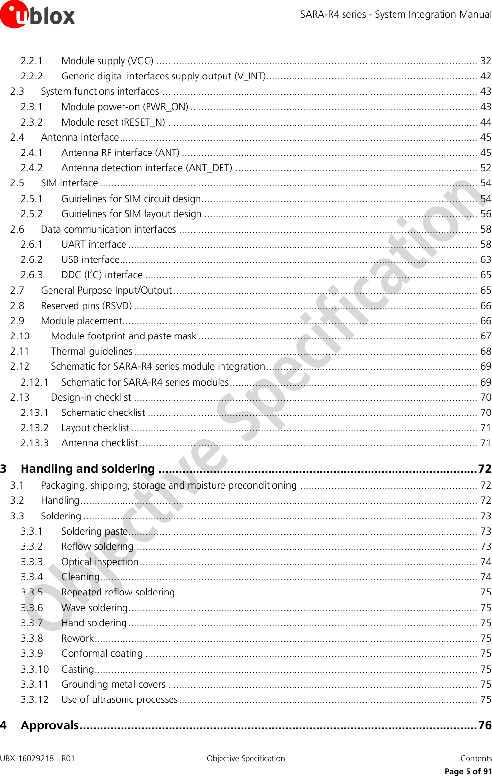
![SARA-R4 series - System Integration Manual UBX-16029218 - R01 Objective Specification System description Page 15 of 91 1.5.1.2 VCC current consumption in connected-mode During an LTE connection, the SARA-R4 module transmits and receives in half duplex mode. The current consumption depends on output RF power, which is always regulated by the network (the current base station) sending power control commands to the module. Figure 3 shows an example of the module current consumption profile versus time in LTE connected-mode. Detailed current consumption values can be found in SARA-R4 series Data Sheet [1]. Time [ms]Current [mA]Current consumption value depends on TX power and actual antenna load0300200100500400600700 Figure 3: VCC current consumption profile versus time during a LTE data connection 1.5.1.3 VCC current consumption in cyclic idle/active mode (power saving enabled) The power saving configuration is by default disabled, but it can be enabled using the AT+UPSV command (see the u-blox SARA-R404M AT Commands Manual [1]). When power saving is enabled, the module automatically enters the low power idle-mode whenever possible, reducing current consumption. During low power idle-mode, the module processor runs with internal 32 kHz reference clock frequency. When the power saving configuration is enabled and the module is registered or attached to a network, the module automatically enters the low power idle-mode whenever possible, but it must periodically monitor the paging channel of the current base station (paging block reception), in accordance to the LTE system requirements. When the module monitors the paging channel, it wakes up to the active-mode, to enable the reception of paging block. In between, the module switches to low power idle-mode. This is known as discontinuous reception (DRX). The module processor core is activated during the paging block reception, and automatically switches its reference clock frequency from 32 kHz to the 19.2 MHz used in active-mode. The time period between two paging block receptions is defined by the network. This is the paging period parameter, fixed by the base station through broadcast channel sent to all users on the same serving cell.](https://usermanual.wiki/u-blox/2AGQN1NNN/User-Guide-3327358-Page-15.png)
![SARA-R4 series - System Integration Manual UBX-16029218 - R01 Objective Specification System description Page 16 of 91 1.5.1.4 VCC current consumption in fixed active-mode (power saving disabled) When power saving is disabled, the module does not automatically enter the low power idle-mode whenever possible: the module remains in active-mode. Power saving configuration is by default disabled. It can also be disabled using the AT+UPSV command (see u-blox SARA-R404M AT Commands Manual [1] for detail usage). The module processor core is activated during idle-mode, and the 19.2 MHz reference clock frequency is used. It would draw more current during the paging period than that in the power saving mode. 1.5.2 Generic digital interfaces supply output (V_INT) The V_INT output pin of the SARA-R4 series modules is generated by the module internal power management circuitry. The typical operating voltage is 1.8 V, whereas the current capability is specified in the SARA-R4 series Data Sheet [1]. The V_INT voltage domain can be used in place of an external discrete regulator as a reference voltage rail for external components.](https://usermanual.wiki/u-blox/2AGQN1NNN/User-Guide-3327358-Page-16.png)
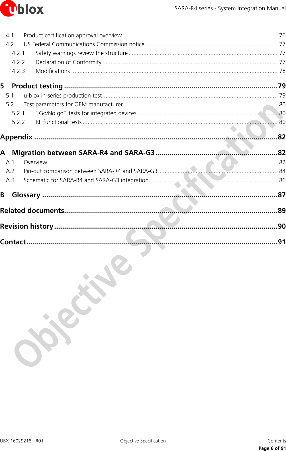
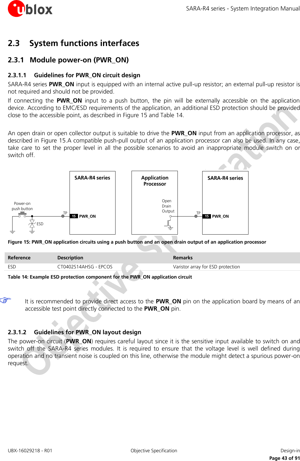
![SARA-R4 series - System Integration Manual UBX-16029218 - R01 Objective Specification System description Page 17 of 91 1.6 System function interfaces 1.6.1 Module power-on When the SARA-R4 series modules are in the not-powered mode (i.e. the VCC module supply is not applied), they can be switched on as follows: Rising edge on the VCC input pins to a valid voltage level and then the PWR_ON input pin is held low for a valid time. After the module power on event, the PWR_ON pin can be released. When the SARA-R4 series modules are in the power-off mode (i.e. switched off with a valid VCC supply applied), they can be switched on as follows: Low pulse on the PWR_ON pin for a valid time period The PWR_ON input pin is equipped with an internal active pull-up resistor. Detailed electrical characteristics with voltages and timings are described in SARA-R4 series Data Sheet [1]. Figure 4 shows the module switch-on sequence from the not-powered mode, describing the following phases: The external power supply is applied to the VCC module pins The PWR_ON pin is held low for a valid time All the generic digital pins of the module are tri-stated until the switch-on of their supply source (V_INT). The internal reset signal is held low: the baseband core and all the digital pins are held in the reset state. When the internal reset signal is released, any digital pin is set in a proper sequence from the reset state to the default operational configured state. The duration of this pins’ configuration phase differs within generic digital interfaces and the USB interface due to host / device enumeration timings (see section 1.9.2). The module is fully ready to operate after all interfaces are configured. Figure 4: SARA-R4 series switch-on sequence description The Internal Reset signal is not available on a module pin, but the host application can monitor the V_INT pin to sense the start of the SARA-R4 series module switch-on sequence. Before the switch-on of the generic digital interface supply source (V_INT) of the module, no voltage driven by an external application should be applied to any generic digital interface of the module. Before the SARA-R4 series module is fully ready to operate, the host application processor should not send any AT command over the AT communication interfaces (USB, UART) of the module. VCCPWR_ONRESET_NV_INTInternal ResetSystem StateBB Pads StateInternal Reset → Operational OperationalTristate / Floating Internal ResetOFFONStart of interface configurationModule interfaces are configuredStart-up event](https://usermanual.wiki/u-blox/2AGQN1NNN/User-Guide-3327358-Page-17.png)
![SARA-R4 series - System Integration Manual UBX-16029218 - R01 Objective Specification System description Page 18 of 91 1.6.2 Module power-off SARA-R4 series can be properly switched off by: AT+CPWROFF command (see u-blox SARA-R404M AT Commands Manual [1]). The current parameter settings are saved in the module’s non-volatile memory and a proper network detach is performed. Low pulse on the PWR_ON pin for a valid time period (see SARA-R4 series Data Sheet [1] ). An abrupt under-voltage shutdown occurs on SARA-R4 series modules when the VCC module supply is removed. If this occurs, it is not possible to perform the storing of the current parameter settings in the module’s non-volatile memory or to perform the proper network detach. It is highly recommended to avoid an abrupt removal of the VCC supply during SARA-R4 series modules normal operations. An abrupt hardware shutdown occurs on SARA-R4 series modules when a low level is applied on RESET_N pin. In this case, the current parameter settings are not saved in the module’s non-volatile memory and a proper network detach is not performed. It is highly recommended to avoid an abrupt hardware shutdown of the module by forcing a low level on the RESET_N input pin during module normal operation: the RESET_N line should be set low only if reset or shutdown via AT commands fails or if the module does not reply to a specific AT command after a time period longer than the one defined in the u-blox SARA-R404M AT Commands Manual [1]. An over-temperature or an under-temperature shutdown occurs on SARA-R4 series modules when the temperature measured within the cellular module reaches the dangerous area, if the optional Smart Temperature Supervisor feature is enabled and configured by the dedicated AT command. For more details see section 1.12.9 and u-blox SARA-R404M AT Commands Manual [1], +USTS AT command. Figure 5 describes the SARA-R4 series modules switch-off sequence started SARA-R4 by means of the AT+CPWROFF command, allowing storage of current parameter settings in the module’s non-volatile memory and a proper network detach, with the following phases: When the +CPWROFF AT command is sent, the module starts the switch-off routine. The module replies OK on the AT interface: the switch-off routine is in progress. At the end of the switch-off routine, all the digital pins are tri-stated and all the internal voltage regulators are turned off, including the generic digital interfaces supply (V_INT). Then, the module remains in switch-off mode as long as a switch on event does not occur (e.g. applying a proper low level to the PWR_ON input pin), and enters not-powered mode if the supply is removed from the VCC pins.](https://usermanual.wiki/u-blox/2AGQN1NNN/User-Guide-3327358-Page-18.png)
![SARA-R4 series - System Integration Manual UBX-16029218 - R01 Objective Specification System description Page 19 of 91 Figure 5: SARA-R4 series switch-off sequence by means of AT+CPWROFF command The Internal Reset signal is not available on a module pin, but the application can monitor the V_INT pin to sense the end of the switch-off sequence. The duration of each phase in the SARA-R4 series modules’ switch-off routines can largely vary depending on the application / network settings and the concurrent module activities. Figure 6 describes the SARA-R4 series modules switch-off sequence started by means of the PWR_ON input pin, allowing storage of current parameter settings in the module’s non-volatile memory and a proper network detach, with the following phases: A low pulse with appropriate time duration (see SARA-R4 series Data Sheet [1]) is applied at the PWR_ON input pin. At the end of the switch-off routine, all the digital pins are tri-stated and all the internal voltage regulators are turned off, including the generic digital interfaces supply (V_INT). Then, the module remains in power-off mode as long as a switch on event does not occur (e.g. applying a proper low level to the PWR_ON input), and enters not-powered mode if the supply is removed from the VCC pins. VCC PWR_ONRESET_N V_INTInternal ResetSystem StateBB Pads StateOFFTristate / FloatingONOperational -> TristateOperational0 s~2.5 s~5 sThe module starts the switch-off routineVCC can be removed Figure 6: SARA-R4 series switch-off sequence by means of PWR_ON pin VCC PWR_ONRESET_N V_INTInternal ResetSystem StateBB Pads State OperationalOFFTristate / FloatingONOperational → TristateAT+CPWROFFsent to the module0 s~2.5 s~5 sOKreplied by the moduleVCC can be removed](https://usermanual.wiki/u-blox/2AGQN1NNN/User-Guide-3327358-Page-19.png)
![SARA-R4 series - System Integration Manual UBX-16029218 - R01 Objective Specification System description Page 20 of 91 The Internal Reset signal is not available on a module pin, but the application can monitor the V_INT pin to sense the end of the switch-off sequence. The duration of each phase in the SARA-R4 series modules’ switch-off routines can largely vary depending on the application / network settings and the concurrent module activities. 1.6.3 Module reset SARA-R4 series modules can be properly reset (rebooted) by: AT+CFUN command (see u-blox SARA-R404M AT Commands Manual [1]). In the case listed above an “internal” or “software” reset of the module is executed: the current parameter settings are saved in the module’s non-volatile memory and a proper network detach is performed. An abrupt hardware shutdown occurs on SARA-R4 series modules when a low level is applied on RESET_N input pin. In this case, the current parameter settings are not saved in the module’s non-volatile memory and a proper network detach is not performed. Then, the module remains in power-off mode as long as a switch on event does not occur applying a proper low level to the PWR_ON input. It is highly recommended to avoid an abrupt hardware reset of the module by forcing a low level on the RESET_N input during modules normal operation: the RESET_N line should be set low only if reset or shutdown via AT commands fails or if the module does not provide a reply to a specific AT command after a time period longer than the one defined in the u-blox SARA-R404M AT Commands Manual [1]. The RESET_N input pin is equipped with an internal pull-up to the V_INT supply. For more electrical characteristics details see SARA-R4 series Data Sheet [1].](https://usermanual.wiki/u-blox/2AGQN1NNN/User-Guide-3327358-Page-20.png)
![SARA-R4 series - System Integration Manual UBX-16029218 - R01 Objective Specification System description Page 21 of 91 1.7 Antenna interface 1.7.1 Antenna RF interface (ANT) SARA-R4 series modules provide an RF interface for connecting the external antenna. The ANT pin represents the primary RF input/output for transmission and reception of LTE RF signals. The ANT pin has a nominal characteristic impedance of 50 and must be connected to the primary Tx / Rx antenna through a 50 transmission line to allow proper RF transmission and reception. 1.7.1.1 Antenna RF interfaces requirements Table 7 summarizes the requirements for the antenna RF interface. See section 2.4.1 for suggestions to properly design antennas circuits compliant with these requirements. The antenna circuits affect the RF compliance of the device integrating SARA-R4 series modules with applicable required certification schemes (for more details see section 4). Compliance is guaranteed if the antenna RF interface requirements summarized in Table 7 are fulfilled. Item Requirements Remarks Impedance 50 nominal characteristic impedance The impedance of the antenna RF connection must match the 50 impedance of the ANT port. Frequency Range See the SARA-R4 series Data Sheet [1] The required frequency range of the antenna connected to ANT port depends on the operating bands of the used cellular module and the used mobile network. Return Loss S11 < -10 dB (VSWR < 2:1) recommended S11 < -6 dB (VSWR < 3:1) acceptable The Return loss or the S11, as the VSWR, refers to the amount of reflected power, measuring how well the antenna RF connection matches the 50 characteristic impedance of the ANT port. The impedance of the antenna termination must match as much as possible the 50 nominal impedance of the ANT port over the operating frequency range, reducing as much as possible the amount of reflected power. Efficiency > -1.5 dB ( > 70% ) recommended > -3.0 dB ( > 50% ) acceptable The radiation efficiency is the ratio of the radiated power to the power delivered to antenna input: the efficiency is a measure of how well an antenna receives or transmits. The radiation efficiency of the antenna connected to the ANT port needs to be enough high over the operating frequency range to comply with the Over-The-Air (OTA) radiated performance requirements, as Total Radiated Power (TRP) and the Total Isotropic Sensitivity (TIS), specified by applicable related certification schemes. Maximum Gain According to radiation exposure limits The power gain of an antenna is the radiation efficiency multiplied by the directivity: the gain describes how much power is transmitted in the direction of peak radiation to that of an isotropic source. The maximum gain of the antenna connected to ANT port must not exceed the herein stated value to comply with regulatory agencies radiation exposure limits. For additional info see sections 4.2.2 and/or 0. Input Power > 24 dBm ( > 0.25 W ) The antenna connected to the ANT port must support with adequate margin the maximum power transmitted by the modules. Table 7: Summary of Tx/Rx antenna RF interface requirements](https://usermanual.wiki/u-blox/2AGQN1NNN/User-Guide-3327358-Page-21.png)
![SARA-R4 series - System Integration Manual UBX-16029218 - R01 Objective Specification System description Page 22 of 91 1.7.2 Antenna detection interface (ANT_DET) The antenna detection is based on ADC measurement. The ANT_DET pin is an Analog to Digital Converter (ADC) provided to sense the antenna presence. The antenna detection function provided by ANT_DET pin is an optional feature that can be implemented if the application requires it. The antenna detection is forced by the +UANTR AT command. See the u-blox SARA-R404M AT Commands Manual [1] for more details on this feature. The ANT_DET pin generates a DC current (for detailed characteristics see the SARA-R4 series Data Sheet [1]) and measures the resulting DC voltage, thus determining the resistance from the antenna connector provided on the application board to GND. So, the requirements to achieve antenna detection functionality are the following: an RF antenna assembly with a built-in resistor (diagnostic circuit) must be used an antenna detection circuit must be implemented on the application board See section 2.4.2 for antenna detection circuit on application board and diagnostic circuit on antenna assembly design-in guidelines. 1.8 SIM interface 1.8.1 SIM interface SARA-R4 series modules provide high-speed SIM/ME interface including automatic detection and configuration of the voltage required by the connected SIM card or chip. Both 1.8 V and 3 V SIM types are supported. Activation and deactivation with automatic voltage switch from 1.8 V to 3 V are implemented, according to ISO-IEC 7816-3 specifications. The VSIM supply output provides internal short circuit protection to limit start-up current and protect the SIM to short circuits. The SIM driver supports the PPS (Protocol and Parameter Selection) procedure for baud-rate selection, according to the values determined by the SIM card or chip. 1.8.2 SIM detection interface (SIM_DET) The SIM_DET pin is configured as an external interrupt to detect the SIM card mechanical / physical presence. The pin is configured as input with an internal active pull-down enabled, and it can sense SIM card presence only if properly connected to the mechanical switch of a SIM card holder as described in section 2.5: Low logic level at SIM_DET input pin is recognized as SIM card not present High logic level at SIM_DET input pin is recognized as SIM card present For more details see the u-blox SARA-R404M AT Commands Manual [1]).](https://usermanual.wiki/u-blox/2AGQN1NNN/User-Guide-3327358-Page-22.png)
![SARA-R4 series - System Integration Manual UBX-16029218 - R01 Objective Specification System description Page 23 of 91 1.9 Data communication interfaces SARA-R4 series modules provide the following serial communication interface: UART interface: Universal Asynchronous Receiver/Transmitter serial interface available for the communication with a host application processor (AT commands, data communication, FW update by means of FOAT) and for diagnostic. (see section 1.9.1) USB interface: Universal Serial Bus 2.0 compliant interface available for the communication with a host application processor (AT commands, data communication, FW update by means of the FOAT feature), for FW update by means of the u-blox EasyFlash tool and for diagnostic. (see section 1.9.2) DDC interface: I2C bus compatible interface available for the communication with u-blox GNSS positioning chips or modules and with external I2C devices (see section 1.9.3) 1.9.1 UART interface 1.9.1.1 UART features The UART interface is a 9-wire 1.8 V unbalanced asynchronous serial interface available on all the SARA-R4 series modules, supporting: AT command mode1 Data mode and Online command mode1 Multiplexer protocol functionality FW upgrades by means of the FOAT feature (see 1.12.8) Trace log capture (diagnostic purpose) UART interface provides RS-232 functionality conforming to the ITU-T V.24 Recommendation [5], with CMOS compatible signal levels: 0 V for low data bit or ON state, and 1.8 V for high data bit or OFF state (for detailed electrical characteristics see SARA-R4 series Data Sheet [1]), providing: data lines (RXD as output, TXD as input), hardware flow control lines (CTS as output, RTS as input), modem status and control lines (DTR as input, DSR as output, DCD as output, RI as output). SARA-R4 series modules are designed to operate as cellular modems, i.e. as the data circuit-terminating equipment (DCE) according to the ITU-T V.24 Recommendation [5]. A host application processor connected to the module through the UART interface represents the data terminal equipment (DTE). UART signal names of the cellular modules conform to the ITU-T V.24 Recommendation [5]: e.g. TXD line represents data transmitted by the DTE (host processor output) and received by the DCE (module input). SARA-R4 series modules’ UART interface is by default configured in AT command mode: the module waits for AT command instructions and interprets all the characters received as commands to execute. All the functionalities supported by SARA-R4 series modules can be in general set and configured by AT commands: AT commands according to 3GPP TS 27.007 [6], 3GPP TS 27.005 [7], 3GPP TS 27.010 [8] u-blox AT commands (for the complete list and syntax see the u-blox SARA-R404M AT Commands Manual [1]) 1 For the definition of the interface data mode, command mode and online command mode see the u-blox SARA-R404M AT Commands Manual [1]](https://usermanual.wiki/u-blox/2AGQN1NNN/User-Guide-3327358-Page-23.png)
![SARA-R4 series - System Integration Manual UBX-16029218 - R01 Objective Specification System description Page 24 of 91 Flow control handshakes are supported by the UART interface and can be set by appropriate AT commands (see u-blox SARA-R404M AT Commands Manual [1], &K, \Q AT commands): hardware flow control (over the RTS / CTS lines), software flow control (XON/XOFF), or none flow control. Hardware flow control is enabled by default. The autobauding is not supported The following baud rates can be configured by AT command (see u-blox SARA-R404M AT Commands Manual [1]): 115200 b/s, default value The following frame formats can be configured by AT command (see u-blox SARA-R404M AT Commands Manual [1]): 8N1 (8 data bits, No parity, 1 stop bit), default frame configuration with fixed baud rate, see Figure 7 D0 D1 D2 D3 D4 D5 D6 D7Start of 1-BytetransferStart Bit(Always 0)Possible Start ofnext transferStop Bit(Always 1)tbit = 1/(Baudrate)Normal Transfer, 8N1 Figure 7: Description of UART 8N1 frame format (8 data bits, no parity, 1 stop bit) 2 2 1.9.1.2 UART signals behavior At the module switch-on, before the UART interface initialization (as described in the power-on sequence reported in Figure 4), each pin is first tri-stated and then is set to its relative internal reset state4. At the end of the boot sequence, the UART interface is initialized, the module is by default in active-mode, and the UART interface is enabled as AT commands interface. The configuration and the behavior of the UART signals after the boot sequence are described below. See section 1.4 for definition and description of module operating modes referred to in this section. RXD signal behavior The module data output line (RXD) is set by default to the OFF state (high level) at UART initialization. The module holds RXD in the OFF state until the module transmits some data. 2 For the definition of the interface data mode, command mode and online command mode see the u-blox SARA-R404M AT Commands Manual [1] 3 Not supported by “02” product versions 4 See the pin description table in the SARA-R4 series Data Sheet [1]](https://usermanual.wiki/u-blox/2AGQN1NNN/User-Guide-3327358-Page-24.png)
![SARA-R4 series - System Integration Manual UBX-16029218 - R01 Objective Specification System description Page 26 of 91 CTS signal behavior The module hardware flow control output (CTS line) is set to the ON state (low level) at UART initialization. If the hardware flow control is enabled, as it is by default, the CTS line indicates when the UART interface is enabled (data can be received): the module drives the CTS line to the ON state or to the OFF state when it is either able or not able to accept data from the DTE over the UART. If hardware flow control is enabled, then when the CTS line is OFF it does not necessarily mean that the module is in low power idle-mode, but only that the UART is not enabled, as the module could be forced to stay in active-mode for other activities, e.g. related to the network or related to other interfaces. The CTS hardware flow control setting can be changed by AT commands (for more details, see the u-blox SARA-R404M AT Commands Manual [1], AT&K, AT\Q AT commands). When the power saving configuration is enabled by AT+UPSV command and the hardware flow-control is not implemented in the DTE/DCE connection, data sent by the DTE can be lost: the first character sent when the module is in low power idle-mode will not be a valid communication character. RTS signal behavior The hardware flow control input (RTS line) is set by default to the OFF state (high level) at UART initialization. The module then holds the RTS line in the OFF state if the line is not activated by the DTE: an active pull-up is enabled inside the module on the RTS input. If the HW flow control is enabled, as it is by default, the module monitors the RTS line to detect permission from the DTE to send data to the DTE itself. If the RTS line is set to the OFF state, any on-going data transmission from the module is interrupted until the RTS line changes to the ON state. The module behavior according to the RTS hardware flow control status can be configured by AT commands (for more details, see the u-blox SARA-R404M AT Commands Manual [1], AT&K, AT\Q, AT+IFC AT commands). If AT+UPSV=2 is set and HW flow control is disabled, the module monitors the RTS line to manage the power saving configuration (for more details, see u-blox SARA-R404M AT Commands Manual [1], AT+UPSV): When an OFF-to-ON transition occurs on the RTS input, the UART is enabled and the module is forced to active-mode. After ~20 ms, the switch is completed and data can be received without loss. The module cannot enter low power idle-mode and the UART is enabled as long as the RTS is in the ON state If the RTS input line is set to the OFF state by the DTE, the UART is disabled (held in low power mode) and the module automatically enters low power idle-mode whenever possible 1.9.2 USB interface 1.9.2.1 USB features SARA-R4 series modules include a High-Speed USB 2.0 compliant interface with 480 Mb/s maximum data rate, representing the main interface for transferring high speed data with a host application processor, supporting: AT command mode6 Data mode and Online command mode6 FW upgrades by means of the FOAT feature (see 1.12.8 and u-blox SARA-R404M AT Commands Manual [1]) 5 See the u-blox SARA-R404M AT Commands Manual [1] for the definition of the interface data mode, command mode and online command mode. 6 For the definition of the interface data mode, command mode and online command mode see the u-blox SARA-R404M AT Commands Manual [1]](https://usermanual.wiki/u-blox/2AGQN1NNN/User-Guide-3327358-Page-26.png)
![SARA-R4 series - System Integration Manual UBX-16029218 - R01 Objective Specification System description Page 27 of 91 FW upgrades by means of the u-blox EasyFlash tool Trace log capture (diagnostic purpose) The module itself acts as a USB device and can be connected to a USB host such as a Personal Computer or an embedded application microprocessor equipped with compatible drivers. The USB_D+/USB_D- lines carry USB serial bus data and signaling according to the Universal Serial Bus Revision 2.0 specification [4], while the VUSB_DET input pin senses the VBUS USB supply presence (nominally 5 V at the source) to detect the host connection and enable the interface. The USB interface of the module is enabled only if a valid voltage is detected by the VUSB_DET input (see the SARA-R4 series Data Sheet [1]). Neither the USB interface, nor the whole module is supplied by the VUSB_DET input: the VUSB_DET senses the USB supply voltage and absorbs few microamperes. The USB interface is controlled and operated with: AT commands according to 3GPP TS 27.007 [6], 3GPP TS 27.005 [7] u-blox AT commands (for the complete list and syntax see u-blox SARA-R404M AT Commands Manual [1]) The USB interface of SARA-R4 series modules can provide the following USB functions: AT commands and data communication Diagnostic log The USB profile of SARA-R4 series modules identifies itself by the following VID (Vendor ID) and PID (Product ID) combination, included in the USB device descriptor according to the USB 2.0 specifications [4]. VID = 0x05C6 PID = 0x90B2 1.9.2.2 USB in Windows USB drivers are provided for Windows operating system platforms and should be properly installed / enabled by following the step-by-step instructions available in the EVK-R2xx User Guide [2] or in the Windows Embedded OS USB Driver Installation Application Note [3]. USB drivers are available for the following operating system platforms: Windows 7 Windows 8 Windows 8.1 Windows 10 Windows Embedded CE 6.0 Windows Embedded Compact 7 Windows Embedded Compact 2013 The module firmware can be upgraded over the USB interface by means of the FOAT feature or using the u-blox EasyFlash tool. 1.9.2.3 USB in Linux/Android It is not required to install a specific driver for each Linux-based or Android-based operating system (OS) to use the module USB interface, which is compatible with standard Linux/Android USB kernel drivers. 1.9.3 DDC (I2C) interface The I2C interface is not supported by “00” product version.](https://usermanual.wiki/u-blox/2AGQN1NNN/User-Guide-3327358-Page-27.png)
![SARA-R4 series - System Integration Manual UBX-16029218 - R01 Objective Specification System description Page 28 of 91 1.10 General Purpose Input/Output SARA-R4 series modules include six pins (GPIO1-GPIO5, SIM_DET) which can be configured as General Purpose Input/Output or to provide custom functions via u-blox AT commands (for more details see the u-blox SARA-R404M AT Commands Manual [1], +UGPIOC, +UGPIOR, +UGPIOW AT commands), as summarized in Table 8. Function Description Default GPIO Configurable GPIOs Network status indication Network status: registered home network, registered roaming, data transmission, no service -- GPIO1-GPIO4 SIM card detection7 External SIM card physical presence detection GPIO5 -- General purpose input Input to sense high or low digital level -- GPIO1-GPIO5 General purpose output Output to set the high or the low digital level -- GPIO1-GPIO5 Pin disabled Tri-state with an internal active pull-down enabled GPIO1-GPIO5 GPIO1-GPIO5 Table 8: SARA-R4 series GPIO custom functions configuration 1.11 Reserved pins (RSVD) SARA-R4 series modules have pins reserved for future use, marked as RSVD: they can all be left unconnected on the application board. 1.12 System features 1.12.1 Network indication GPIOs can be configured by the AT command to indicate network status (for further details see section 1.10 and the u-blox SARA-R404M AT Commands Manual [1]): No service (no network coverage or not registered) Registered to the home network Registered to the visitor network (roaming) Data call enabled (RF data transmission / reception) 1.12.2 Antenna supervisor The antenna detection function provided by the ANT_DET pin is based on an ADC measurement as optional feature that can be implemented if the application requires it. The antenna supervisor is forced by the +UANTR AT command (see the u-blox SARA-R404M AT Commands Manual [1] for more details). The requirements to achieve antenna detection functionality are the following: an RF antenna assembly with a built-in resistor (diagnostic circuit) must be used an antenna detection circuit must be implemented on the application board See section 1.7.2 for detailed antenna detection interface functional description and see section 2.4.2 for detection circuit on application board and diagnostic circuit on antenna assembly design-in guidelines. 1.12.3 Dual stack IPv4/IPv6 SARA-R4 series support both Internet Protocol version 4 and Internet Protocol version 6 in parallel. For more details about dual stack IPv4/IPv6 see the u-blox SARA-R404M AT Commands Manual [1]. 7 Not supported by “00” product version](https://usermanual.wiki/u-blox/2AGQN1NNN/User-Guide-3327358-Page-28.png)
![SARA-R4 series - System Integration Manual UBX-16029218 - R01 Objective Specification System description Page 29 of 91 1.12.4 TCP/IP and UDP/IP SARA-R4 series modules provide embedded TCP/IP and UDP/IP protocol stack: a PDP context can be configured established and handled via the data connection management packet switched data commands. SARA-R4 series modules provide Direct Link mode to establish a transparent end-to-end communication with an already connected TCP or UDP socket via serial interfaces (USB, UART). In Direct Link mode, data sent to the serial interface from an external application processor is forwarded to the network and vice-versa. For more details about embedded TCP/IP and UDP/IP functionalities see the u-blox SARA-R404M AT Commands Manual [1]. 1.12.5 FTP SARA-R4 series provide embedded File Transfer Protocol (FTP) services. Files are read and stored in the local file system of the module. FTP files can also be transferred using FTP Direct Link: FTP download: data coming from the FTP server is forwarded to the host processor via USB / UART serial interfaces (for FTP without Direct Link mode the data is always stored in the module’s Flash File System) FTP upload: data coming from the host processor via USB / UART serial interface is forwarded to the FTP server (for FTP without Direct Link mode the data is read from the module’s Flash File System) When Direct Link is used for a FTP file transfer, only the file content pass through USB / UART serial interface, whereas all the FTP commands handling is managed internally by the FTP application. For more details about embedded FTP functionalities see u-blox SARA-R404M AT Commands Manual [1]. 1.12.6 HTTP SARA-R4 series modules provide the embedded Hyper-Text Transfer Protocol (HTTP) services via AT commands for sending requests to a remote HTTP server, receiving the server response and transparently storing it in the module’s Flash File System (FFS). For more details about embedded HTTP functionalities see the u-blox SARA-R404M AT Commands Manual [1]. 1.12.7 SSL SARA-R4 series modules support the Secure Sockets Layer (SSL) with certificate key sizes up to 4096 bits to provide security over the FTP and HTTP protocols. The SSL support provides different connection security aspects: Server authentication: use of the server certificate verification against a specific trusted certificate or a trusted certificates list Client authentication: use of the client certificate and the corresponding private key Data security and integrity: data encryption and Hash Message Authentication Code (HMAC) generation The security aspects used during a connection depend on the SSL configuration and features supported. For a complete list of supported configurations and settings see the u-blox SARA-R404M AT Commands Manual [1]. 1.12.8 Firmware update Over AT (FOAT) This feature allows upgrading the module firmware over USB interface, using AT commands. The +FWINSTALL AT command triggers a reboot followed by the upgrade procedure at specified a baud rate A special boot loader on the module performs firmware installation, security verifications and module reboot Firmware authenticity verification is performed via a security signature during the download. The firmware is then installed, overwriting the current version. In case of power loss during this phase, the boot loader](https://usermanual.wiki/u-blox/2AGQN1NNN/User-Guide-3327358-Page-29.png)
![SARA-R4 series - System Integration Manual UBX-16029218 - R01 Objective Specification System description Page 30 of 91 detects a fault at the next wake-up, and restarts the firmware download from the Xmodem-1k handshake. After completing the upgrade, the module is reset again and wakes-up in normal boot For more details about Firmware update Over AT procedure see the the u-blox SARA-R404M AT Commands Manual [1], +UFWUPD AT command. 1.12.9 Power saving The power saving configuration is by default disabled, but it can be enabled using the AT+UPSV command (for the complete description of the AT+UPSV command, see the u-blox SARA-R404M AT Commands Manual [1]). When power saving is enabled, the module automatically enters the low power idle-mode whenever possible, reducing current consumption (see section 1.5.1.3 and SARA-R4 series Data Sheet [1]).For the definition and the description of SARA-R4 series modules operating modes, including the events forcing transitions between the different operating modes, see the section 1.4.](https://usermanual.wiki/u-blox/2AGQN1NNN/User-Guide-3327358-Page-30.png)
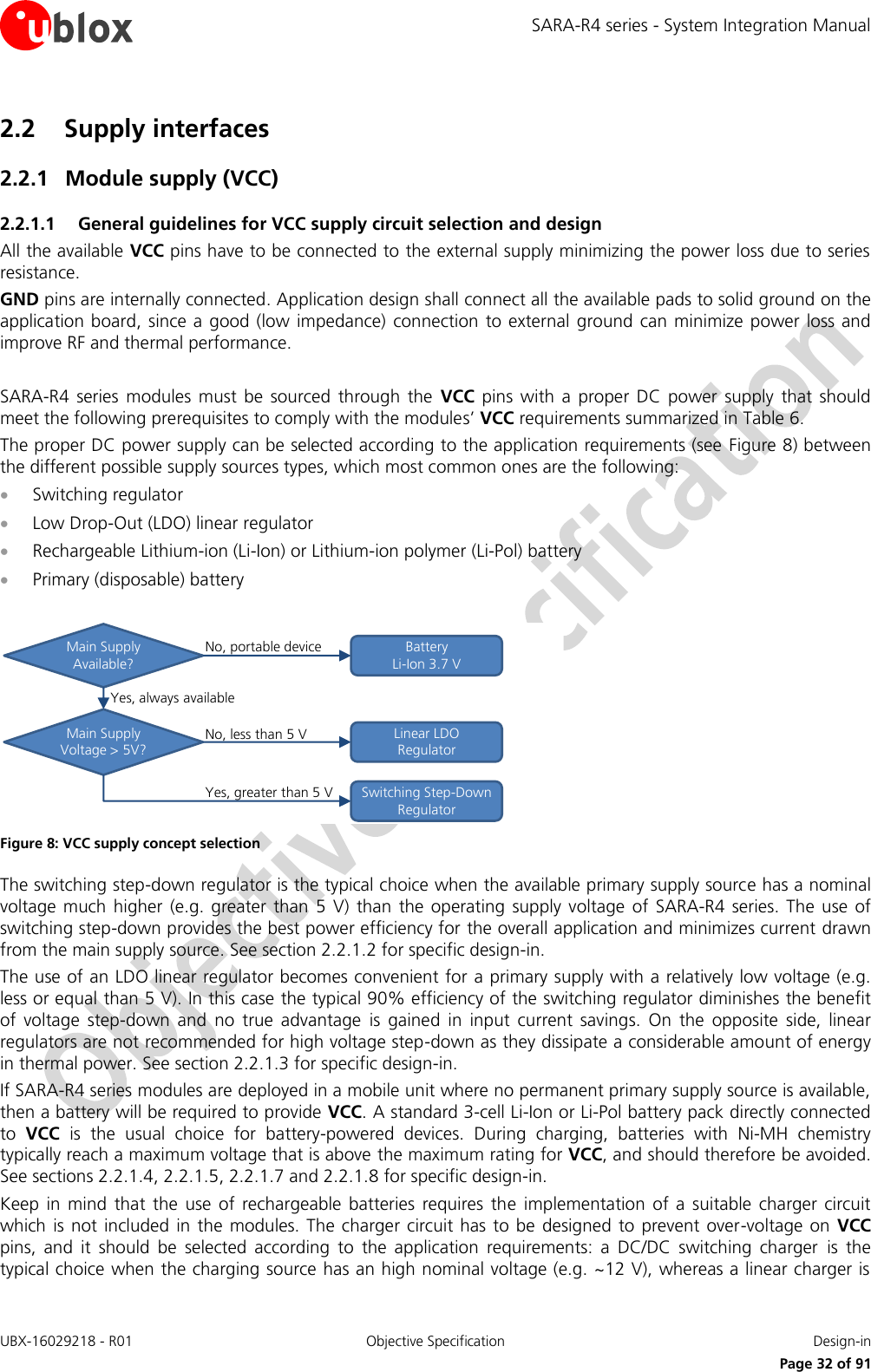
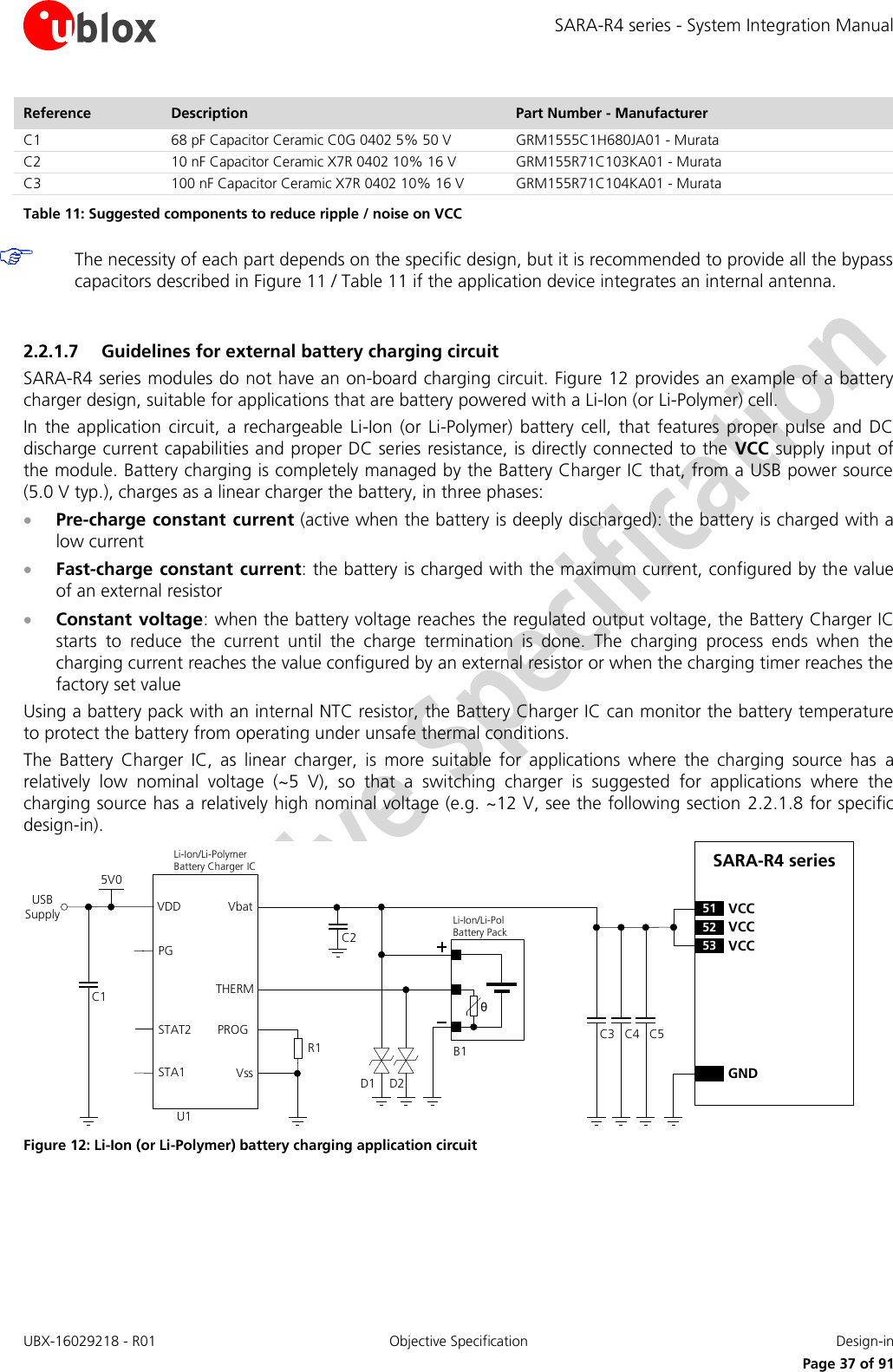
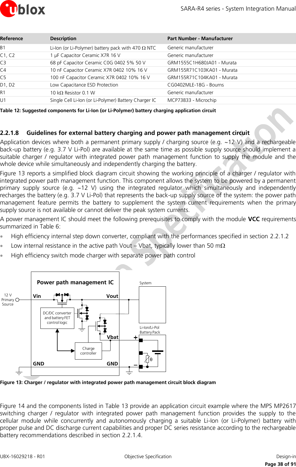
![SARA-R4 series - System Integration Manual UBX-16029218 - R01 Objective Specification Design-in Page 33 of 91 the typical choice when the charging source has a relatively low nominal voltage (~5 V). If both a permanent primary supply / charging source (e.g. ~12 V) and a rechargeable back-up battery (e.g. 3.7 V Li-Pol) are available at the same time as possible supply source, then a proper charger / regulator with integrated power path management function can be selected to supply the module while simultaneously and independently charging the battery. See sections 2.2.1.7 and 2.2.1.8 for specific design-in. An appropriate primary (not rechargeable) battery can be selected taking into account the maximum current specified in SARA-R4 series Data Sheet [1] during connected-mode, considering that primary cells might have weak power capability. See section 2.2.1.5 for specific design-in. The usage of more than one DC supply at the same time should be carefully evaluated: depending on the supply source characteristics, different DC supply systems can result as mutually exclusive. The selected regulator or battery must be able to support with adequate margin the highest averaged current consumption value specified in the SARA-R4 series Data Sheet [1]. The following sections highlight some design aspects for each of the supplies listed above providing application circuit design-in compliant with the module VCC requirements summarized in Table 6. 2.2.1.2 Guidelines for VCC supply circuit design using a switching regulator The use of a switching regulator is suggested when the difference from the available supply rail source to the VCC value is high, since switching regulators provide good efficiency transforming a 12 V or greater voltage supply to the typical 3.8 V value of the VCC supply. The characteristics of the switching regulator connected to VCC pins should meet the following prerequisites to comply with the module VCC requirements summarized in Table 6: Power capability: the switching regulator with its output circuit must be capable of providing a voltage value to the VCC pins within the specified operating range and must be capable of delivering to VCC pins the maximum current consumption occuring during transmissions at the maximum power, as specified in the SARA-R4 series Data Sheet [1]. Low output ripple: the switching regulator together with its output circuit must be capable of providing a clean (low noise) VCC voltage profile. High switching frequency: for best performance and for smaller applications it is recommended to select a switching frequency ≥ 600 kHz (since L-C output filter is typically smaller for high switching frequency). The use of a switching regulator with a variable switching frequency or with a switching frequency lower than 600 kHz must be carefully evaluated since this can produce noise in the VCC voltage profile and therefore negatively impact the LTEmodulation spectrum performance. PWM mode operation: it is preferable to select regulators with Pulse Width Modulation (PWM) mode. While in connected-mode, the Pulse Frequency Modulation (PFM) mode and PFM/PWM modes transitions must be avoided to reduce noise on VCC voltage profile. Switching regulators can be used that are able to switch between low ripple PWM mode and high ripple PFM mode, provided that the mode transition occurs when the module changes status from the idle/active-modes to connected-mode. It is permissible to use a regulator that switches from the PWM mode to the burst or PFM mode at an appropriate current threshold.](https://usermanual.wiki/u-blox/2AGQN1NNN/User-Guide-3327358-Page-33.png)
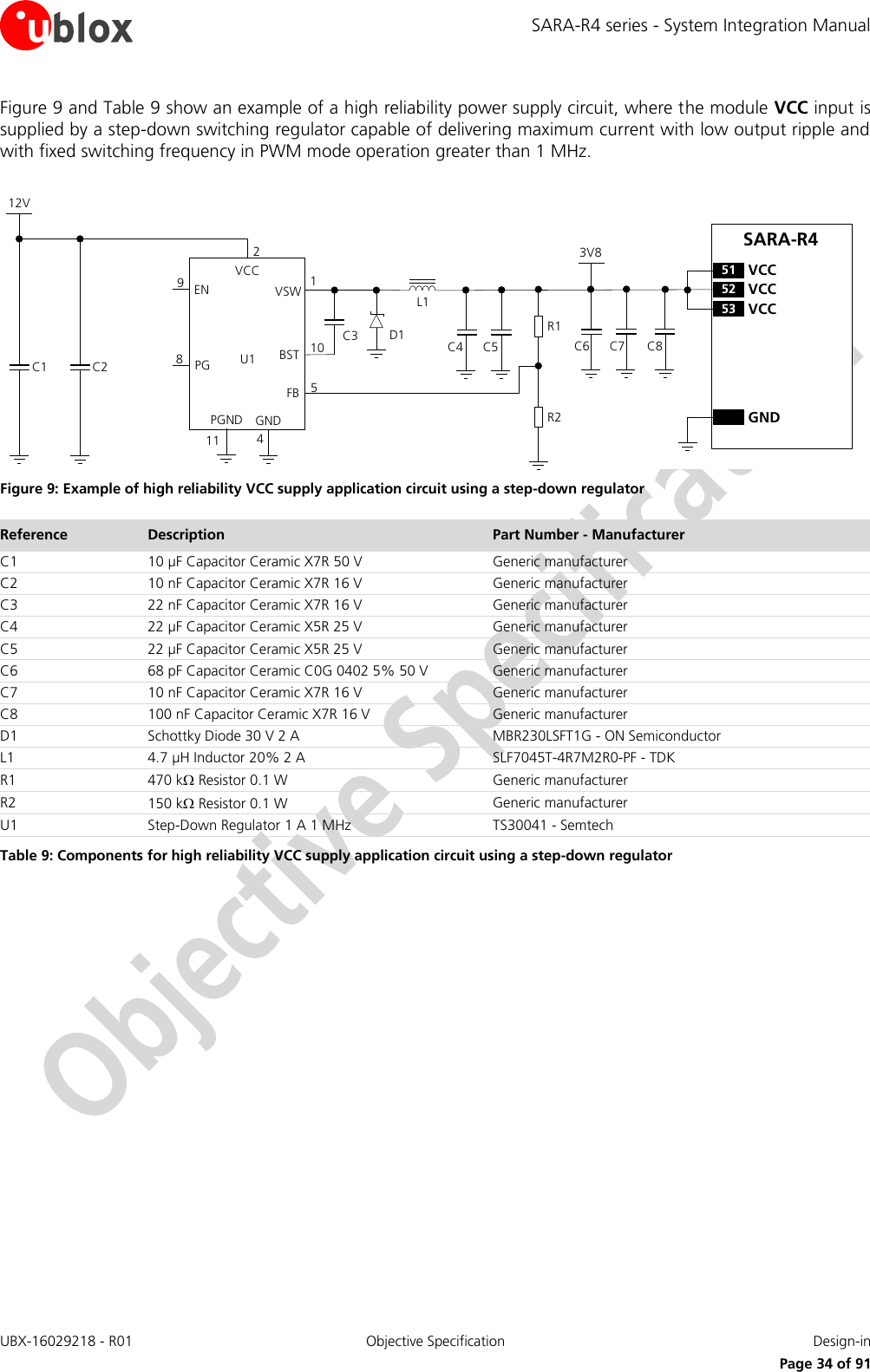
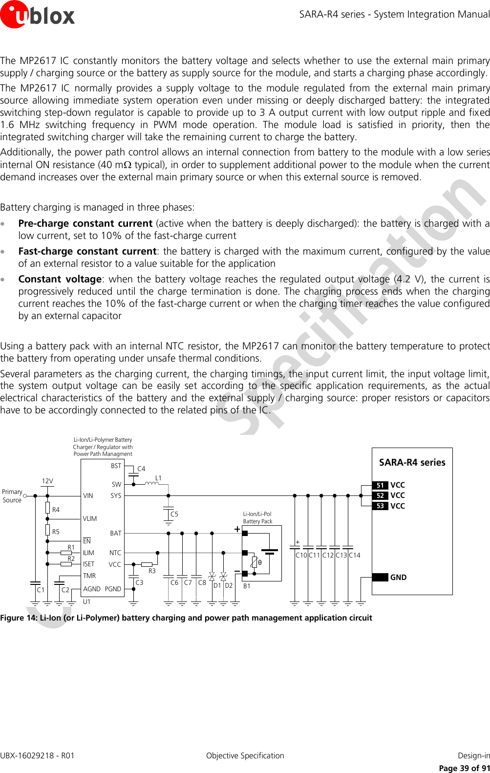
![SARA-R4 series - System Integration Manual UBX-16029218 - R01 Objective Specification Design-in Page 35 of 91 2.2.1.3 Guidelines for VCC supply circuit design using a Low Drop-Out linear regulator The use of a linear regulator is suggested when the difference from the available supply rail source and the VCC value is low. The linear regulators provide high efficiency when transforming a 5 VDC supply to a voltage value within the module VCC normal operating range. The characteristics of the Low Drop-Out (LDO) linear regulator connected to VCC pins should meet the following prerequisites to comply with the module VCC requirements summarized in Table 6: Power capabilities: the LDO linear regulator with its output circuit must be capable of providing a voltage value to the VCC pins within the specified operating range and must be capable of delivering to VCC pins the maximum current consumption occurring during a transmission at the maximum Tx power, as specified in SARA-R4 series Data Sheet [1]. Power dissipation: the power handling capability of the LDO linear regulator must be checked to limit its junction temperature to the maximum rated operating range (i.e. check the voltage drop from the max input voltage to the minimum output voltage to evaluate the power dissipation of the regulator). Figure 10 and the components listed in Table 10 show an example of a power supply circuit, where the VCC module supply is provided by an LDO linear regulator capable of delivering the required current, with proper power handling capability. It is recommended to configure the LDO linear regulator to generate a voltage supply value slightly below the maximum limit of the module VCC normal operating range (e.g. ~4.1 V for the VCC, as in the circuits described in Figure 10 and Table 10). This reduces the power on the linear regulator and improves the thermal design of the circuit. 5VC1 R1IN OUTADJGND58134C2R2R3U1ENSARA-R4 series52 VCC53 VCC51 VCCGNDC4C3 C5 Figure 10: Example of high reliability VCC supply application circuit using an LDO linear regulator Reference Description Part Number - Manufacturer C1 1 µF Capacitor Ceramic X5R 6.3 V Generic manufacturer C2 4.7 µF Capacitor Ceramic X5R 6.3 V Generic manufacturer C3 68 pF Capacitor Ceramic C0G 50 V Generic manufacturer C4 10 nF Capacitor Ceramic X7R 16 V Generic manufacturer C5 100 nF Capacitor Ceramic X7R 16 V Generic manufacturer R1 47 k Resistor 0.1 W Generic manufacturer R2 41 k Resistor 0.1 W Generic manufacturer R3 10 k Resistor 0.1 W Generic manufacturer U1 LDO Linear Regulator 1.0 A AP7361 – Diodes Incorporated Table 10: Components for high reliability VCC supply application circuit using an LDO linear regulator](https://usermanual.wiki/u-blox/2AGQN1NNN/User-Guide-3327358-Page-35.png)
![SARA-R4 series - System Integration Manual UBX-16029218 - R01 Objective Specification Design-in Page 36 of 91 2.2.1.4 Guidelines for VCC supply circuit design using a rechargeable Li-Ion or Li-Pol battery Rechargeable Li-Ion or Li-Pol batteries connected to the VCC pins should meet the following prerequisites to comply with the module VCC requirements summarized in Table 6: Maximum pulse and DC discharge current: the rechargeable Li-Ion battery with its related output circuit connected to the VCC pins must be capable of delivering the maximum current occurring during a transmission at maximum Tx power, as specified in SARA-R4 series Data Sheet [1]. The maximum discharge current is not always reported in the data sheets of batteries, but the maximum DC discharge current is typically almost equal to the battery capacity in Amp-hours divided by 1 hour. DC series resistance: the rechargeable Li-Ion battery with its output circuit must be capable of avoiding a VCC voltage drop below the operating range summarized in Table 6 during transmit bursts. 2.2.1.5 Guidelines for VCC supply circuit design using a primary (disposable) battery The characteristics of a primary (non-rechargeable) battery connected to VCC pins should meet the following prerequisites to comply with the module VCC requirements summarized in Table 6: Maximum pulse and DC discharge current: the non-rechargeable battery with its related output circuit connected to the VCC pins must be capable of delivering the maximum current consumption occurring during a transmission at maximum Tx power, as specified in SARA-R4 series Data Sheet [1]. The maximum discharge current is not always reported in the data sheets of batteries, but the max DC discharge current is typically almost equal to the battery capacity in Amp-hours divided by 1 hour. DC series resistance: the non-rechargeable battery with its output circuit must be capable of avoiding a VCC voltage drop below the operating range summarized in Table 6 during transmit bursts. 2.2.1.6 Additional guidelines for VCC supply circuit design To reduce voltage drops, use a low impedance power source. The series resistance of the power supply lines (connected to the modules’ VCC and GND pins) on the application board and battery pack should also be considered and minimized: cabling and routing must be as short as possible to minimize power losses. Three pins are allocated to VCC supply. Several pins are designated for GND connection. It is recommended to properly connect all of them to supply the module to minimize series resistance losses. To reduce voltage ripple and noise, improving RF performance especially if the application device integrates an internal antenna, place the following bypass capacitors near the VCC pins: 68 pF capacitor with Self-Resonant Frequency in the 800/900 MHz range (e.g. Murata GRM1555C1H680J) 10 nF capacitor (e.g. Murata GRM155R71C103K) to filter digital logic noise from clocks and data sources 100 nF capacitor (e.g. Murata GRM155R61C104K) to filter digital logic noise from clocks and data sources A suitable series ferrite bead can be properly placed on the VCC line for additional noise filtering if required by the specific application according to the whole application board design. C2GNDC3SARA-R4 series52VCC53VCC51VCCC13V8 Figure 11: Suggested schematic for the VCC bypass capacitors to reduce ripple / noise on supply voltage profile](https://usermanual.wiki/u-blox/2AGQN1NNN/User-Guide-3327358-Page-36.png)
![SARA-R4 series - System Integration Manual UBX-16029218 - R01 Objective Specification Design-in Page 42 of 91 2.2.2 Generic digital interfaces supply output (V_INT) 2.2.2.1 Guidelines for V_INT circuit design SARA-R4 series provide the V_INT generic digital interfaces 1.8 V supply output, which can be mainly used to: Indicate when the module is switched on (as described in sections 1.6.1, 1.6.2) Supply voltage translators to connect 1.8 V module generic digital interfaces to 3.0 V devices (e.g. see 2.6.1) Enable external voltage regulators providing supply for external devices, Do not apply loads which might exceed the limit for maximum available current from V_INT supply (see the SARA-R4 series Data Sheet [1]) as this can cause malfunctions in internal circuitry. V_INT can only be used as an output: do not connect any external supply source on V_INT. It is recommended to provide direct access to the V_INT pin on the application board by means of an accessible test point directly connected to the V_INT pin.](https://usermanual.wiki/u-blox/2AGQN1NNN/User-Guide-3327358-Page-42.png)
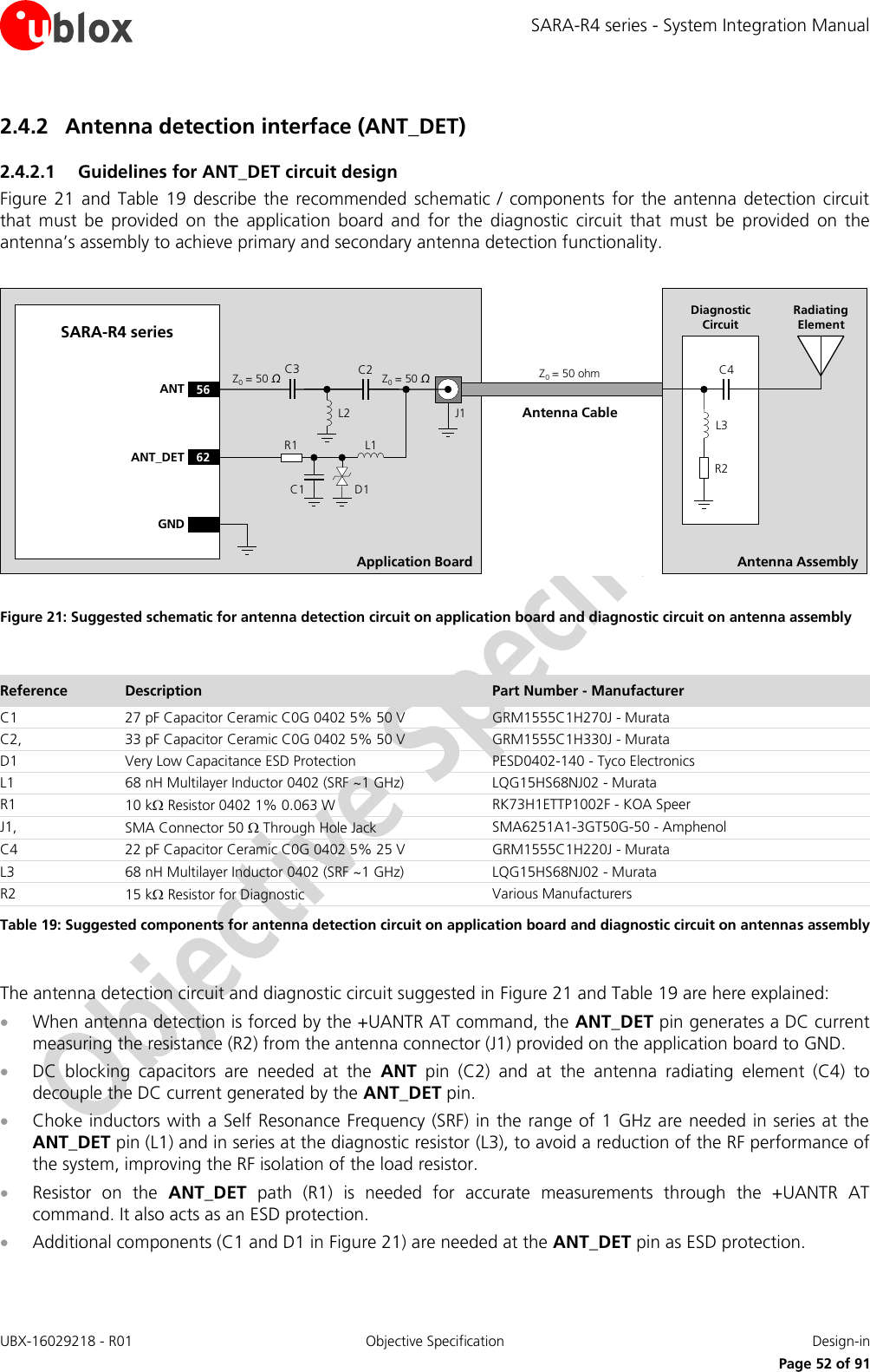
![SARA-R4 series - System Integration Manual UBX-16029218 - R01 Objective Specification Design-in Page 53 of 91 Additional high pass filter (C3 and L2 in Figure 21) is provided at the ANT pin as ESD immunity improvement for SARA-U260, SARA-U270 and SARA-U280 modules (a series 0 jumper can be mounted for SARA-G340 and SARA-G350 modules instead of the high pass filter, as no further precaution to ESD immunity test is needed). The ANT pin must be connected to the antenna connector by means of a transmission line with nominal characteristics impedance as close as possible to 50 . The DC impedance at RF port for some antennas may be a DC open (e.g. linear monopole) or a DC short to reference GND (e.g. PIFA antenna). For those antennas, without the diagnostic circuit of Figure 21, the measured DC resistance is always at the limits of the measurement range (respectively open or short), and there is no mean to distinguish between a defect on antenna path with similar characteristics (respectively: removal of linear antenna or RF cable shorted to GND for PIFA antenna). Furthermore, any other DC signal injected to the RF connection from ANT connector to radiating element will alter the measurement and produce invalid results for antenna detection. It is recommended to use an antenna with a built-in diagnostic resistor in the range from 5 k to 30 k to assure good antenna detection functionality and avoid a reduction of module RF performance. The choke inductor should exhibit a parallel Self Resonance Frequency (SRF) in the range of 1 GHz to improve the RF isolation of load resistor. For example: Consider an antenna with built-in DC load resistor of 15 k. Using the +UANTR AT command, the module reports the resistance value evaluated from the antenna connector provided on the application board to GND: Reported values close to the used diagnostic resistor nominal value (i.e. values from 13 k to 17 k if a 15 k diagnostic resistor is used) indicate that the antenna is properly connected. Values close to the measurement range maximum limit (approximately 50 k) or an open-circuit “over range” report (see u-blox SARA-R404M AT Commands Manual [1]) means that that the antenna is not connected or the RF cable is broken. Reported values below the measurement range minimum limit (1 k) highlights a short to GND at antenna or along the RF cable. Measurement inside the valid measurement range and outside the expected range may indicate an improper connection, damaged antenna or wrong value of antenna load resistor for diagnostic. Reported value could differ from the real resistance value of the diagnostic resistor mounted inside the antenna assembly due to antenna cable length, antenna cable capacity and the used measurement method. If the antenna detection function is not required by the customer application, the ANT_DET pin can be left not connected and the ANT pin can be directly connected to the antenna connector by means of a 50 transmission line as described in Figure 20. 2.4.2.2 Guidelines for ANT_DET layout design The recommended layout for the antenna detection circuit to be provided on the application board to achieve the antenna detection functionality, implementing the recommended schematic described in Figure 21 and Table 19, is explained here: The ANT pin have to be connected to the antenna connector by means of a 50 transmission line, implementing the design guidelines described in section 2.4.1 and the recommendations of the SMA connector manufacturer. DC blocking capacitor at ANT pins (C2, C3) has to be placed in series to the 50 RF line. The ANT_DET pin has to be connected to the 50 transmission line by means of a sense line.](https://usermanual.wiki/u-blox/2AGQN1NNN/User-Guide-3327358-Page-53.png)
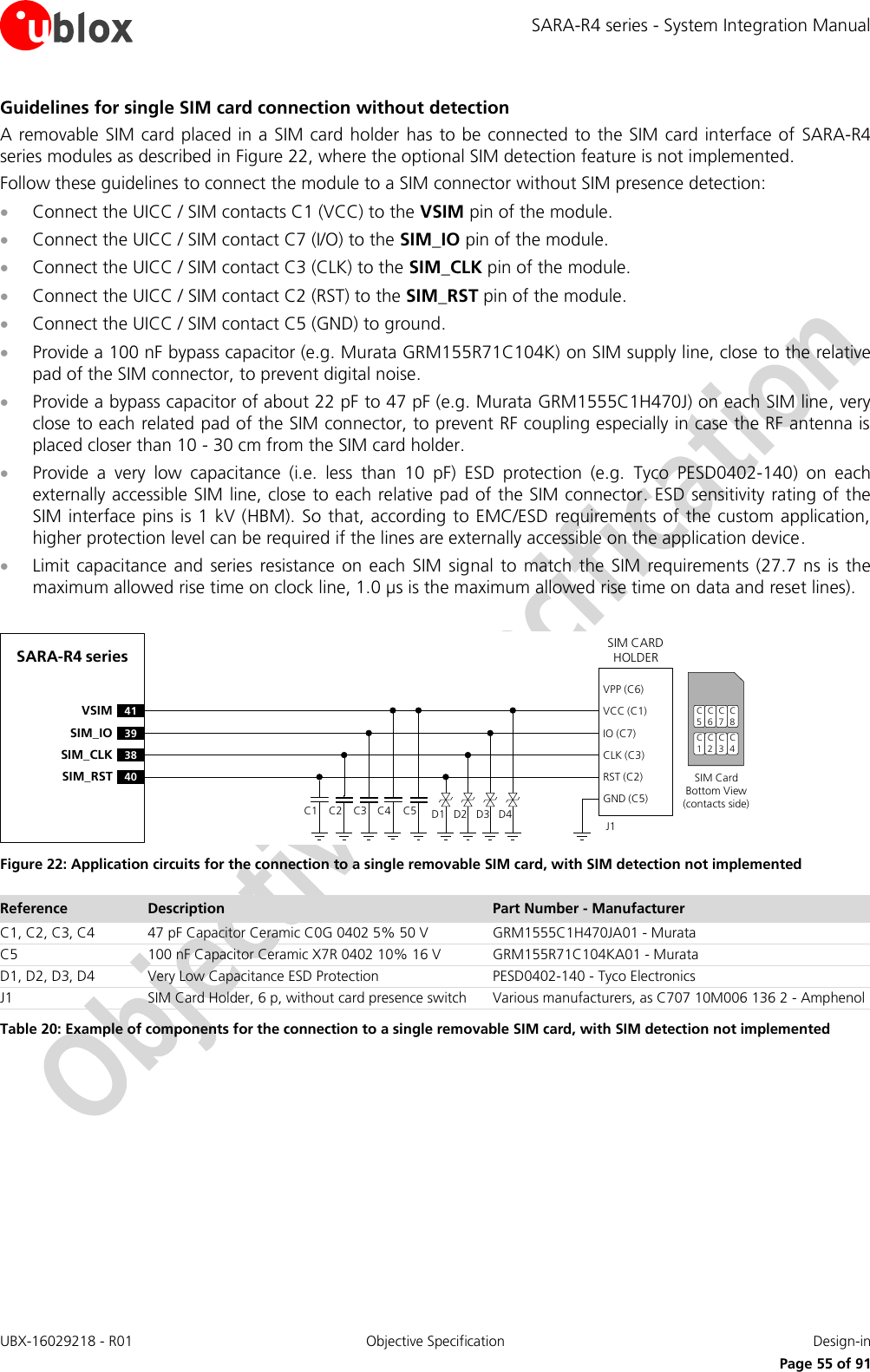
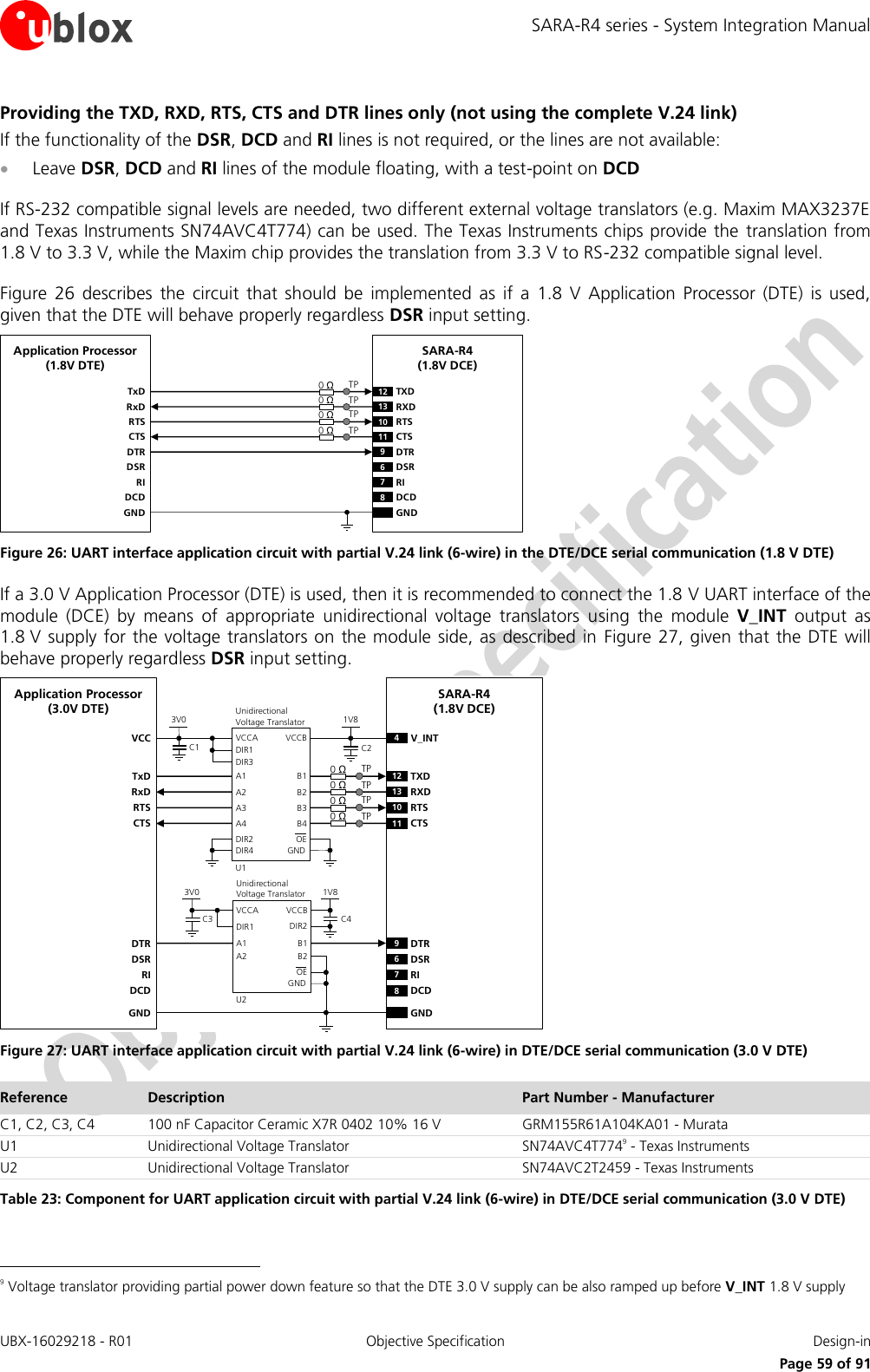
![SARA-R4 series - System Integration Manual UBX-16029218 - R01 Objective Specification Design-in Page 60 of 91 Providing the TXD, RXD, RTS and CTS lines only (not using the complete V.24 link) If the functionality of the DSR, DCD, RI and DTR lines is not required in, or the lines are not available: Connect the module DTR input to GND using a 0 series resistor, since it may be useful to set DTR active if not specifically handled (see u-blox SARA-R404M AT Commands Manual [1], &D, S0, +CSGT, +CNMI AT commands) Leave DSR, DCD and RI lines of the module floating, with a test-point on DCD If RS-232 compatible signal levels are needed, the Maxim MAX13234E voltage level translator can be used. This chip translates voltage levels from 1.8 V (module side) to the RS-232 standard. If a 1.8 V Application Processor is used, the circuit should be implemented as described in Figure 28. TxDApplication Processor(1.8V DTE)RxDRTSCTSDTRDSRRIDCDGNDSARA-R4(1.8V DCE)12 TXD9DTR13 RXD10 RTS11 CTS6DSR7RI8DCDGND0ΩTP0ΩTP0ΩTP0ΩTP Figure 28: UART interface application circuit with partial V.24 link (5-wire) in the DTE/DCE serial communication (1.8V DTE) If a 3.0 V Application Processor (DTE) is used, then it is recommended to connect the 1.8 V UART interface of the module (DCE) by means of appropriate unidirectional voltage translators using the module V_INT output as 1.8 V supply for the voltage translators on the module side, as described in Figure 29. 4V_INTTxDApplication Processor(3.0V DTE)RxDRTSCTSDTRDSRRIDCDGNDSARA-R4 series (1.8V DCE)12 TXD9DTR13 RXD10 RTS11 CTS6DSR7RI8DCDGND1V8B1 A1GNDU1B3A3VCCBVCCAUnidirectionalVoltage TranslatorC1 C23V0DIR3DIR2 OEDIR1VCCB2 A2B4A4DIR4TP0ΩTP0ΩTP0ΩTPTP Figure 29: UART interface application circuit with partial V.24 link (5-wire) in DTE/DCE serial communication (3.0 V DTE) Reference Description Part Number - Manufacturer C1, C2 100 nF Capacitor Ceramic X7R 0402 10% 16 V GRM155R61A104KA01 - Murata U1 Unidirectional Voltage Translator SN74AVC4T77410 - Texas Instruments Table 24: Component for UART application circuit with partial V.24 link (5-wire) in DTE/DCE serial communication (3.0 V DTE) 10 Voltage translator providing partial power down feature so that the DTE 3.0 V supply can be also ramped up before V_INT 1.8 V supply](https://usermanual.wiki/u-blox/2AGQN1NNN/User-Guide-3327358-Page-60.png)
![SARA-R4 series - System Integration Manual UBX-16029218 - R01 Objective Specification Design-in Page 61 of 91 Providing the TXD and RXD lines only (not using the complete V24 link) If the functionality of the CTS, RTS, DSR, DCD, RI and DTR lines is not required in the application, or the lines are not available, then: Connect the module RTS input line to GND or to the CTS output line of the module: since the module requires RTS active (low electrical level) if HW flow-control is enabled (AT&K3, which is the default setting) Connect the module DTR input line to GND using a 0 series resistor, because it is useful to set DTR active if not specifically handled (see u-blox SARA-R404M AT Commands Manual [1], &D, S0, +CSGT, +CNMI AT commands) Leave DSR, DCD and RI lines of the module floating, with a test-point on DCD If RS-232 compatible signal levels are needed, the Maxim MAX13234E voltage level translator can be used. This chip translates voltage levels from 1.8 V (module side) to the RS-232 standard. If a 1.8 V Application Processor (DTE) is used, the circuit that should be implemented as described in Figure 30 TxDApplication Processor(1.8V DTE)RxDRTSCTSDTRDSRRIDCDGNDSARA-R4(1.8V DCE)12 TXD9DTR13 RXD10 RTS11 CTS6DSR7RI8DCDGND0ΩTP0ΩTP0ΩTPTP Figure 30: UART interface application circuit with partial V.24 link (3-wire) in the DTE/DCE serial communication (1.8V DTE) If a 3.0 V Application Processor (DTE) is used, then it is recommended to connect the 1.8 V UART interface of the module (DCE) by means of appropriate unidirectional voltage translators using the module V_INT output as 1.8 V supply for the voltage translators on the module side, as described in Figure 31. 4V_INTTxDApplication Processor(3.0V DTE)RxDDTRDSRRIDCDGNDSARA-R4(1.8V DCE)12 TXD9DTR13 RXD6DSR7RI8DCDGND1V8B1 A1GNDU1VCCBVCCAUnidirectionalVoltage TranslatorC1 C23V0DIR1DIR2 OEVCCB2 A2RTSCTS10 RTS11 CTSTP0ΩTP0ΩTP0ΩTPTP Figure 31: UART interface application circuit with partial V.24 link (3-wire) in DTE/DCE serial communication (3.0 V DTE) Reference Description Part Number - Manufacturer C1, C2 100 nF Capacitor Ceramic X7R 0402 10% 16 V GRM155R61A104KA01 - Murata U1 Unidirectional Voltage Translator SN74AVC2T24511 - Texas Instruments Table 25: Component for UART application circuit with partial V.24 link (3-wire) in DTE/DCE serial communication (3.0 V DTE) 11 Voltage translator providing partial power down feature so that the DTE 3.0 V supply can be also ramped up before V_INT 1.8 V supply](https://usermanual.wiki/u-blox/2AGQN1NNN/User-Guide-3327358-Page-61.png)
![SARA-R4 series - System Integration Manual UBX-16029218 - R01 Objective Specification Design-in Page 63 of 91 2.6.2 USB interface 2.6.2.1 Guidelines for USB circuit design The USB_D+ and USB_D- lines carry the USB serial data and signaling. The lines are used in single ended mode for full speed signaling handshake, as well as in differential mode for high speed signaling and data transfer. USB pull-up or pull-down resistors and external series resistors on USB_D+ and USB_D- lines as required by the USB 2.0 specification [4] are part of the module USB pins driver and do not need to be externally provided. The USB interface of the module is enabled only if a valid voltage is detected by the VUSB_DET input (see the SARA-R4 series Data Sheet [1]). Neither the USB interface, nor the whole module is supplied by the VUSB_DET input: the VUSB_DET senses the USB supply voltage and absorbs few microamperes. Routing the USB pins to a connector, they will be externally accessible on the application device. According to EMC/ESD requirements of the application, an additional ESD protection device with very low capacitance should be provided close to accessible point on the line connected to this pin, as described in Figure 32 and Table 26. The USB pins of the modules can be directly connected to the USB host application processor without additional ESD protections if they are not externally accessible or according to EMC/ESD requirements. D+D-GND29 USB_D+28 USB_D-GNDUSB DEVICE CONNECTORVBUSD+D-GND29 USB_D+28 USB_D-GNDUSB HOST PROCESSORSARA-R4 series SARA-R4 series VBUS 17 VUSB_DET17 VUSB_DETD1 D2 D3 C1 C1 Figure 32: USB Interface application circuits Reference Description Part Number - Manufacturer C1 100 nF Capacitor Ceramic X7R 0402 10% 16 V GRM155R61A104KA01 - Murata D1, D2, D3 Very Low Capacitance ESD Protection PESD0402-140 - Tyco Electronics Table 26: Component for USB application circuits If the USB interface pins are not used, they can be left unconnected on the application board, but it is recommended providing accessible test points directly connected to VUSB_DET, USB_D+, USB_D- pins.](https://usermanual.wiki/u-blox/2AGQN1NNN/User-Guide-3327358-Page-63.png)
![SARA-R4 series - System Integration Manual UBX-16029218 - R01 Objective Specification Design-in Page 64 of 91 2.6.2.2 Guidelines for USB layout design The USB_D+ / USB_D- lines require accurate layout design to achieve reliable signaling at the high speed data rate (up to 480 Mb/s) supported by the USB serial interface. The characteristic impedance of the USB_D+ / USB_D- lines is specified by the Universal Serial Bus Revision 2.0 specification [4]. The most important parameter is the differential characteristic impedance applicable for the odd-mode electromagnetic field, which should be as close as possible to 90 differential. Signal integrity may be degraded if PCB layout is not optimal, especially when the USB signaling lines are very long. Use the following general routing guidelines to minimize signal quality problems: Route USB_D+ / USB_D- lines as a differential pair Route USB_D+ / USB_D- lines as short as possible Ensure the differential characteristic impedance (Z0) is as close as possible to 90 Ensure the common mode characteristic impedance (ZCM) is as close as possible to 30 Consider design rules for USB_D+ / USB_D- similar to RF transmission lines, being them coupled differential micro-strip or buried stripline: avoid any stubs, abrupt change of layout, and route on clear PCB area Figure 33 and Figure 34 provide two examples of coplanar waveguide designs with differential characteristic impedance close to 90 and common mode characteristic impedance close to 30 . The first transmission line can be implemented in case of 4-layer PCB stack-up herein described, the second transmission line can be implemented in case of 2-layer PCB stack-up herein described. 35 µm35 µm35 µm35 µm270 µm270 µm760 µmL1 CopperL3 CopperL2 CopperL4 CopperFR-4 dielectricFR-4 dielectricFR-4 dielectric350 µm 400 µm400 µm350 µm400 µm Figure 33: Example of USB line design, with Z0 close to 90 and ZCM close to 30 , for the described 4-layer board layup 35 µm35 µm1510 µmL2 CopperL1 CopperFR-4 dielectric740 µm 410 µm410 µm740 µm410 µm Figure 34: Example of USB line design, with Z0 close to 90 and ZCM close to 30 , for the described 2-layer board layup](https://usermanual.wiki/u-blox/2AGQN1NNN/User-Guide-3327358-Page-64.png)
![SARA-R4 series - System Integration Manual UBX-16029218 - R01 Objective Specification Design-in Page 68 of 91 2.11 Thermal guidelines The module operating temperature range is specified in SARA-R4 series Data Sheet [1]. The most critical condition concerning module thermal performance is the uplink transmission at maximum power (data upload in connected-mode), when the baseband processor runs at full speed, radio circuits are all active and the RF power amplifier is driven to higher output RF power. This scenario is not often encountered in real networks (for example, see the Terminal Tx Power distribution for WCDMA, taken from operation on a live network, described in the GSMA TS.09 Battery Life Measurement and Current Consumption Technique [12]); however the application should be correctly designed to cope with it. During transmission at maximum RF power the SARA-R4 series modules generate thermal power that may exceed 2 W: this is an indicative value since the exact generated power strictly depends on operating condition such as the actual antenna return loss, the transmitting frequency band, etc. The generated thermal power must be adequately dissipated through the thermal and mechanical design of the application. The spreading of the Module-to-Ambient thermal resistance (Rth,M-A) depends on the module operating condition. The overall temperature distribution is influenced by the configuration of the active components during the specific mode of operation and their different thermal resistance toward the case interface. The Module-to-Ambient thermal resistance value and the relative increase of module temperature will differ according to the specific mechanical deployments of the module, e.g. application PCB with different dimensions and characteristics, mechanical shells enclosure, or forced air flow. The increase of the thermal dissipation, i.e. the reduction of the Module-to-Ambient thermal resistance, will decrease the temperature of the modules’ internal circuitry for a given operating ambient temperature. This improves the device long-term reliability in particular for applications operating at high ambient temperature. Recommended hardware techniques to be used to improve heat dissipation in the application: Connect each GND pin with solid ground layer of the application board and connect each ground area of the multilayer application board with complete thermal via stacked down to main ground layer. Provide a ground plane as wide as possible on the application board. Optimize antenna return loss, to optimize overall electrical performance of the module including a decrease of module thermal power. Optimize the thermal design of any high-power components included in the application, such as linear regulators and amplifiers, to optimize overall temperature distribution in the application device. Select the material, the thickness and the surface of the box (i.e. the mechanical enclosure) of the application device that integrates the module so that it provides good thermal dissipation. Further hardware techniques that may be considered to improve the heat dissipation in the application: Force ventilation air-flow within mechanical enclosure. Provide a heat sink component attached to the module top side, with electrically insulated / high thermal conductivity adhesive, or on the backside of the application board, below the cellular module, as a large part of the heat is transported through the GND pads of the SARA-R4 series LGA modules and dissipated over the backside of the application board. For example, the Module-to-Ambient thermal resistance (Rth,M-A) is strongly reduced with forced air ventilation and a heat-sink installed on the back of the application board, decreasing the module temperature variation. Beside the reduction of the Module-to-Ambient thermal resistance implemented by proper application hardware design, the increase of module temperature can be moderated by proper application software implementation: Enable power saving configuration using the AT+UPSV command Enable module connected-mode for a given time period and then disable it for a time period enough long to properly mitigate temperature increase.](https://usermanual.wiki/u-blox/2AGQN1NNN/User-Guide-3327358-Page-68.png)
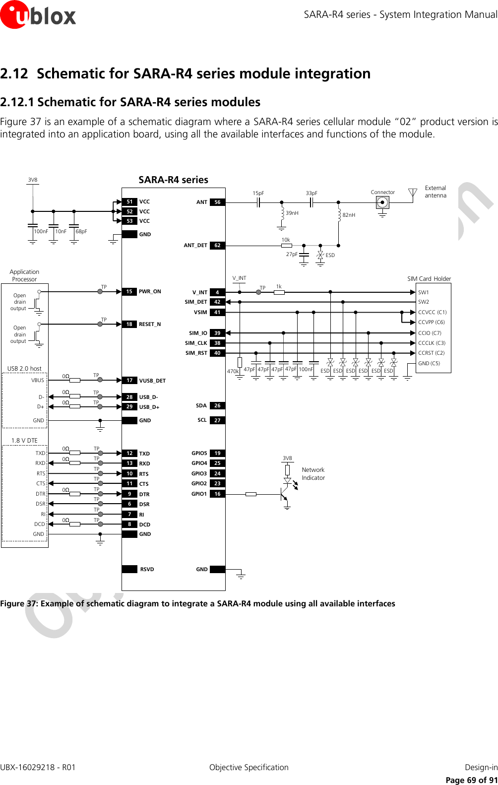
![SARA-R4 series - System Integration Manual UBX-16029218 - R01 Objective Specification Design-in Page 70 of 91 2.13 Design-in checklist This section provides a design-in checklist. 2.13.1 Schematic checklist The following are the most important points for a simple schematic check: DC supply must provide a nominal voltage at VCC pin within the operating range limits. DC supply must be capable of supporting the highest averaged current consumption values in connected-mode, as specified in the SARA-R4 series Data Sheet [1]. VCC voltage supply should be clean, with very low ripple/noise: provide the suggested bypass capacitors, in particular if the application device integrates an internal antenna. Do not apply loads which might exceed the limit for maximum available current from V_INT supply. Check that voltage level of any connected pin does not exceed the relative operating range. Provide accessible test points directly connected to the following pins of the SARA-R4 series modules: V_INT, PWR_ON and RESET_N for diagnostic purpose. Capacitance and series resistance must be limited on each SIM signal to match the SIM specifications. Insert the suggested pF capacitors on each SIM signal and low capacitance ESD protections if accessible. Check UART signals direction, as the modules’ signal names follow the ITU-T V.24 Recommendation [5]. Provide accessible test points directly connected to all the UART pins of the SARA-R4 series modules (TXD, RXD, DTR, DCD) for diagnostic purpose, in particular providing a 0 series jumper on each line to detach each UART pin of the module from the DTE application processor. Capacitance and series resistance must be limited on each high speed line of the USB interface. If the USB is not used, provide accessible test points directly connected to the USB interface (VUSB_DET, USB_D+ and USB_D- pins). Use transistors with at least an integrated resistor in the base pin or otherwise put a 10 k resistor on the board in series to the GPIO when those are used to drive LEDs. Provide proper precautions for EMC / ESD immunity as required on the application board. Do not apply voltage to any generic digital interface pin of SARA-R4 series modules before the switch-on of the generic digital interface supply source (V_INT). All unused pins can be left unconnected.](https://usermanual.wiki/u-blox/2AGQN1NNN/User-Guide-3327358-Page-70.png)
![SARA-R4 series - System Integration Manual UBX-16029218 - R01 Objective Specification Handling and soldering Page 72 of 91 3 Handling and soldering No natural rubbers, no hygroscopic materials or materials containing asbestos are employed. 3.1 Packaging, shipping, storage and moisture preconditioning For information pertaining to SARA-R4 series reels / tapes, Moisture Sensitivity levels (MSD), shipment and storage information, as well as drying for preconditioning, see the SARA-R4 series Data Sheet [1] and the u-blox Package Information Guide [23]. 3.2 Handling The SARA-R4 series modules are Electro-Static Discharge (ESD) sensitive devices. Ensure ESD precautions are implemented during handling of the module. Electrostatic discharge (ESD) is the sudden and momentary electric current that flows between two objects at different electrical potentials caused by direct contact or induced by an electrostatic field. The term is usually used in the electronics and other industries to describe momentary unwanted currents that may cause damage to electronic equipment. The ESD sensitivity for each pin of SARA-R4 series modules (as Human Body Model according to JESD22-A114F) is specified in the SARA-R4 series Data Sheet [1]. ESD prevention is based on establishing an Electrostatic Protective Area (EPA). The EPA can be a small working station or a large manufacturing area. The main principle of an EPA is that there are no highly charging materials near ESD sensitive electronics, all conductive materials are grounded, workers are grounded, and charge build-up on ESD sensitive electronics is prevented. International standards are used to define typical EPA and can be obtained for example from International Electrotechnical Commission (IEC) or American National Standards Institute (ANSI). In addition to standard ESD safety practices, the following measures should be taken into account whenever handling the SARA-R4 series modules: Unless there is a galvanic coupling between the local GND (i.e. the work table) and the PCB GND, then the first point of contact when handling the PCB must always be between the local GND and PCB GND. Before mounting an antenna patch, connect ground of the device. When handling the module, do not come into contact with any charged capacitors and be careful when contacting materials that can develop charges (e.g. patch antenna, coax cable, soldering iron,…). To prevent electrostatic discharge through the RF pin, do not touch any exposed antenna area. If there is any risk that such exposed antenna area is touched in non ESD protected work area, implement proper ESD protection measures in the design. When soldering the module and patch antennas to the RF pin, make sure to use an ESD safe soldering iron.](https://usermanual.wiki/u-blox/2AGQN1NNN/User-Guide-3327358-Page-72.png)
![SARA-R4 series - System Integration Manual UBX-16029218 - R01 Objective Specification Handling and soldering Page 74 of 91 To avoid falling off, modules should be placed on the topside of the motherboard during soldering. The soldering temperature profile chosen at the factory depends on additional external factors like choice of soldering paste, size, thickness and properties of the base board, etc. Exceeding the maximum soldering temperature and the maximum liquidus time limit in the recommended soldering profile may permanently damage the module. Preheat Heating Cooling[°C] Peak Temp. 245°C [°C]250 250Liquidus Temperature217 217200 20040 - 60 sEnd Temp.max 4°C/s150 - 200°C150 150max 3°C/s60 - 120 s100 Typical Leadfree 100Soldering Profile50 50Elapsed time [s] Figure 38: Recommended soldering profile The modules must not be soldered with a damp heat process. 3.3.3 Optical inspection After soldering the SARA-R4 series modules, inspect the modules optically to verify that the module is properly aligned and centered. 3.3.4 Cleaning Cleaning the modules is not recommended. Residues underneath the modules cannot be easily removed with a washing process. Cleaning with water will lead to capillary effects where water is absorbed in the gap between the baseboard and the module. The combination of residues of soldering flux and encapsulated water leads to short circuits or resistor-like interconnections between neighboring pads. Water will also damage the sticker and the ink-jet printed text. Cleaning with alcohol or other organic solvents can result in soldering flux residues flooding into the two housings, areas that are not accessible for post-wash inspections. The solvent will also damage the sticker and the ink-jet printed text. Ultrasonic cleaning will permanently damage the module, in particular the quartz oscillators. For best results use a "no clean" soldering paste and eliminate the cleaning step after the soldering.](https://usermanual.wiki/u-blox/2AGQN1NNN/User-Guide-3327358-Page-74.png)
![SARA-R4 series - System Integration Manual UBX-16029218 - R01 Objective Specification Approvals Page 76 of 91 4 Approvals For the complete list and specific details regarding the certification schemes approvals, see SARA-R4 series Data Sheet [1], or please contact the u-blox office or sales representative nearest you. 4.1 Product certification approval overview Product certification approval is the process of certifying that a product has passed all tests and criteria required by specifications, typically called “certification schemes” that can be divided into three distinct categories: Regulatory certification o Country specific approval required by local government in most regions and countries, such as: CE (Conformité Européenne) marking for European Union FCC (Federal Communications Commission) approval for United States Industry certification o Telecom industry specific approval verifying the interoperability between devices and networks: GCF (Global Certification Forum), partnership between European device manufacturers and network operators to ensure and verify global interoperability between devices and networks PTCRB (PCS Type Certification Review Board), created by United States network operators to ensure and verify interoperability between devices and North America networks Operator certification o Operator specific approval required by some mobile network operator, such as: AT&T network operator in United States Verizon Wireless network operator in United States Even if SARA-R4 series modules are approved under all major certification schemes, the application device that integrates SARA-R4 series modules must be approved under all the certification schemes required by the specific application device to be deployed in the market. The required certification scheme approvals and relative testing specifications differ depending on the country or the region where the device that integrates SARA-R4 series modules must be deployed, on the relative vertical market of the device, on type, features and functionalities of the whole application device, and on the network operators where the device must operate. Check the appropriate applicability of the SARA-R4 series module’s approvals while starting the certification process of the device integrating the module: the re-use of the u-blox cellular module’s approval can significantly reduce the cost and time to market of the application device certification. The certification of the application device that integrates a SARA-R4 series module and the compliance of the application device with all the applicable certification schemes, directives and standards are the sole responsibility of the application device manufacturer. SARA-R4 series modules are certified according to all capabilities and options stated in the Protocol Implementation Conformance Statement document (PICS) of the module. The PICS, according to the 3GPP TS 51.010-2 [17], 3GPP TS 34.121-2 [18], 3GPP TS 36.521-2 [20] and 3GPP TS 36.523-2 [21], is a statement of the implemented and supported capabilities and options of a device. The PICS document of the application device integrating SARA-R4 series modules must be updated from the module PICS statement if any feature stated as supported by the module in its PICS document is not implemented or disabled in the application device. For more details regarding the AT commands settings that affect the PICS, see the u-blox SARA-R404M AT Commands Manual [1]. Check the specific settings required for mobile network operators approvals as they may differ from the AT commands settings defined in the module as integrated in the application device.](https://usermanual.wiki/u-blox/2AGQN1NNN/User-Guide-3327358-Page-76.png)
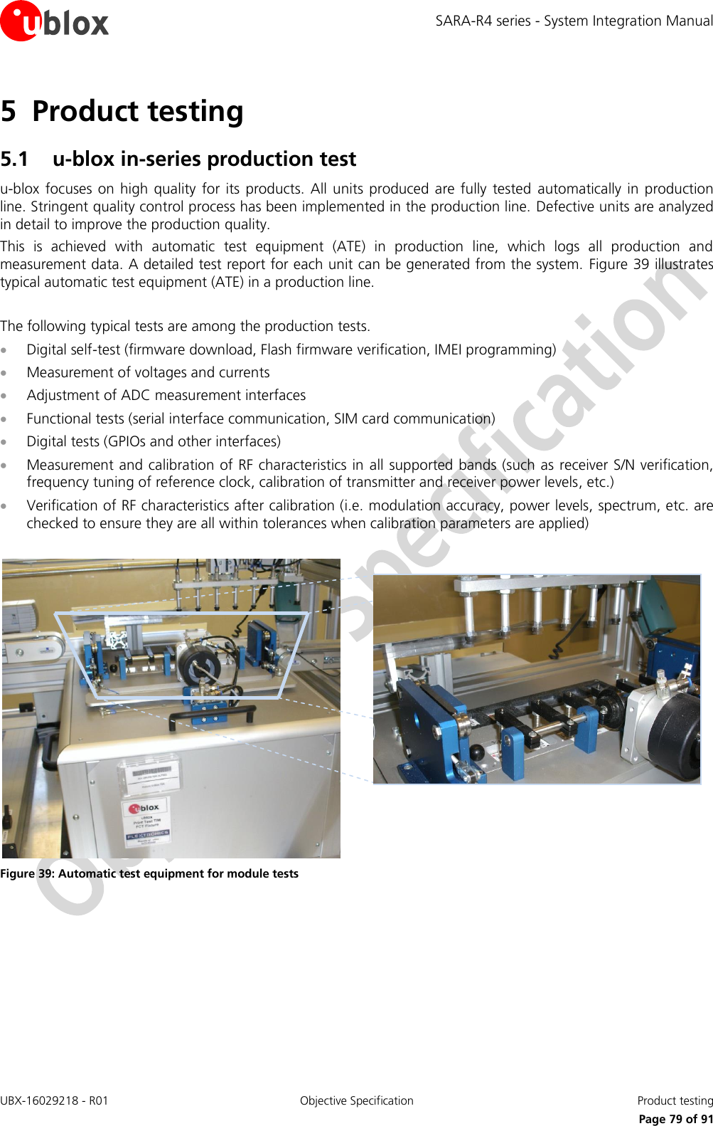
![SARA-R4 series - System Integration Manual UBX-16029218 - R01 Objective Specification Product testing Page 80 of 91 5.2 Test parameters for OEM manufacturer Because of the testing done by u-blox (with 100% coverage), an OEM manufacturer does not need to repeat firmware tests or measurements of the module RF performance or tests over analog and digital interfaces in their production test. However, an OEM manufacturer should focus on: Module assembly on the device; it should be verified that: o Soldering and handling process did not damage the module components o All module pins are well soldered on device board o There are no short circuits between pins Component assembly on the device; it should be verified that: o Communication with host controller can be established o The interfaces between module and device are working o Overall RF performance test of the device including antenna Dedicated tests can be implemented to check the device. For example, the measurement of module current consumption when set in a specified status can detect a short circuit if compared with a “Golden Device” result. In addition, module AT commands can be used to perform functional tests on digital interfaces (communication with host controller, check SIM interface, GPIOs, etc.) or to perform RF performance tests (see the following section 5.2.2 for details). 5.2.1 “Go/No go” tests for integrated devices A “Go/No go” test is typically to compare the signal quality with a “Golden Device” in a location with excellent network coverage and known signal quality. This test should be performed after data connection has been established. These kinds of test may be useful as a “go/no go” test but not for RF performance measurements. This test is suitable to check the functionality of communication with host controller, SIM card as well as power supply. It is also a means to verify if components at antenna interface are well soldered. 5.2.2 RF functional tests The overall RF functional test of the device including the antenna can be performed with basic instruments such as a spectrum analyzer (or an RF power meter) and a signal generator with the assistance of AT+UTEST command over AT command user interface. The AT+UTEST command provides a simple interface to set the module to Rx or Tx test modes ignoring the LTE signaling protocol. The command can set the module into: transmitting mode in a specified channel and power level in all supported modulation schemes and bands receiving mode in a specified channel to returns the measured power level in all supported bands See the u-blox SARA-R404M AT Commands Manual [1] and the End user test Application Note [22], for the AT+UTEST command syntax description and detail guide of usage.](https://usermanual.wiki/u-blox/2AGQN1NNN/User-Guide-3327358-Page-80.png)
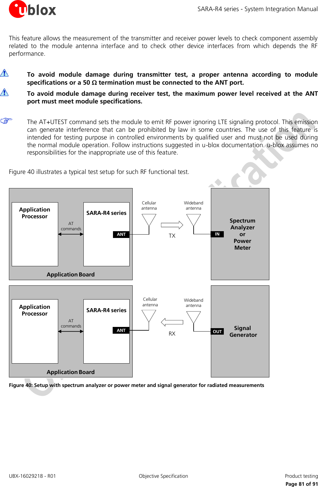
![SARA-R4 series - System Integration Manual UBX-16029218 - R01 Objective Specification Appendix Page 82 of 91 Appendix A Migration between SARA-R4 and SARA-G3 A.1 Overview SARA-G3 and SARA-R4 series cellular modules have exactly the same SARA form factor (26.0 x 16.0 mm LGA) with exactly the same 96-pin layout as described in Figure 41, so that the modules can be alternatively mounted on a single application board using exactly the same copper mask, solder mask and paste mask. 64 63 61 60 58 57 55 5422 23 25 26 28 29 31 3211108754212119181615131243444647495052533335363839414265 66 67 68 69 7071 72 73 74 75 7677 7879 8081 8283 8485 86 87 88 89 9091 92 93 94 95 96CTSRTSDCDRIV_INTV_BCKPGNDRSVDRESET_NRSVDPWR_ONRXDTXD32017149624 27 305148454037345962 56GNDGNDDSRDTRGNDRSVDGNDGNDRXD_AUXTXD_AUXEXT32KGNDRSVD32K_OUTRSVDRSVDRSVDGNDGNDGNDRSVDRSVDRSVDRSVDGNDVCCVCCRSVDRSVDRSVDSIM_CLKSIM_IOVSIMSIM_DETVCCRSVDRSVDSIM_RSTRSVDRSVDGNDGNDGNDGNDGNDGNDGNDGNDGNDRSVDANTSARA-G300 SARA-G310Top ViewPin 65-96: GND64 63 61 60 58 57 55 5422 23 25 26 28 29 31 3211108754212119181615131243444647495052533335363839414265 66 67 68 69 7071 72 73 74 75 7677 7879 8081 8283 8485 86 87 88 89 9091 92 93 94 95 96CTSRTSDCDRIV_INTV_BCKPGNDRSVDRESET_NGPIO1PWR_ONRXDTXD32017149624 27 305148454037345962 56GNDGNDDSRDTRGNDRSVDGNDGNDRXD_AUXTXD_AUXRSVDGNDGPIO2GPIO3SDASCLGPIO4GNDGNDGNDSPK_PMIC_BIASMIC_GNDMIC_PGNDVCCVCCRSVDI2S_TXDI2S_CLKSIM_CLKSIM_IOVSIMSIM_DETVCCMIC_NSPK_NSIM_RSTI2S_RXDI2S_WAGNDGNDGNDGNDGNDGNDGNDGNDGNDANT_DETANTSARA-G340SARA-G350Top ViewPin 65-96: GND64 63 61 60 58 57 55 5422 23 25 26 28 29 31 3211108754212119181615131243444647495052533335363839414265 66 67 68 69 7071 72 73 74 75 7677 7879 8081 8283 8485 86 87 88 89 9091 92 93 94 95 96CTSRTSDCDRIV_INTRSVDPGNDCODEC_CLKRESET_NGPIO1PWR_ONRXDTXD32017149624 27 305148454037345962 56GNDGNDDSRDTRGNDVUSB_DETGNDGNDUSB_D-USB_D+RSVDGNDGPIO2GPIO3SDASCLGPIO4GNDGNDGNDRSVDRSVDRSVDRSVDGNDVCCVCCRSVDRSVDRSVDSIM_CLKSIM_IOVSIMSIM_DETVCCRSVDRSVDSIM_RSTRSVDRSVDGNDGNDGNDGNDGNDGNDGNDGNDGNDANT_DETANTSARA-R4Top ViewPin 65-96: GND Figure 41: SARA-R4 and SARA-R4 seriesSARA-G3 series modules pad layout and pin assignment SARA modules are also form-factor compatible with the u-blox LISA, LARA and TOBY cellular module families: although each has a different form factor, the footprints for the TOBY, LISA, SARA and LARA modules have been developed to ensure layout compatibility. With the u-blox “nested design” solution, any TOBY, LISA, SARA or LARA module can be alternatively mounted on the same space of a single “nested” application board as described in Figure 42. Guidelines in order to implement a nested application board, description of the u-blox reference nested design and comparison between TOBY, LISA, SARA and LARA modules are provided in the Nested Design Application Note [26]. LISA cellular moduleLARA cellular moduleSARA cellular moduleNested application boardTOBY cellular module Figure 42: TOBY, LISA, SARA, LARA modules’ layout compatibility: all modules are accommodated on the same nested footprint](https://usermanual.wiki/u-blox/2AGQN1NNN/User-Guide-3327358-Page-82.png)
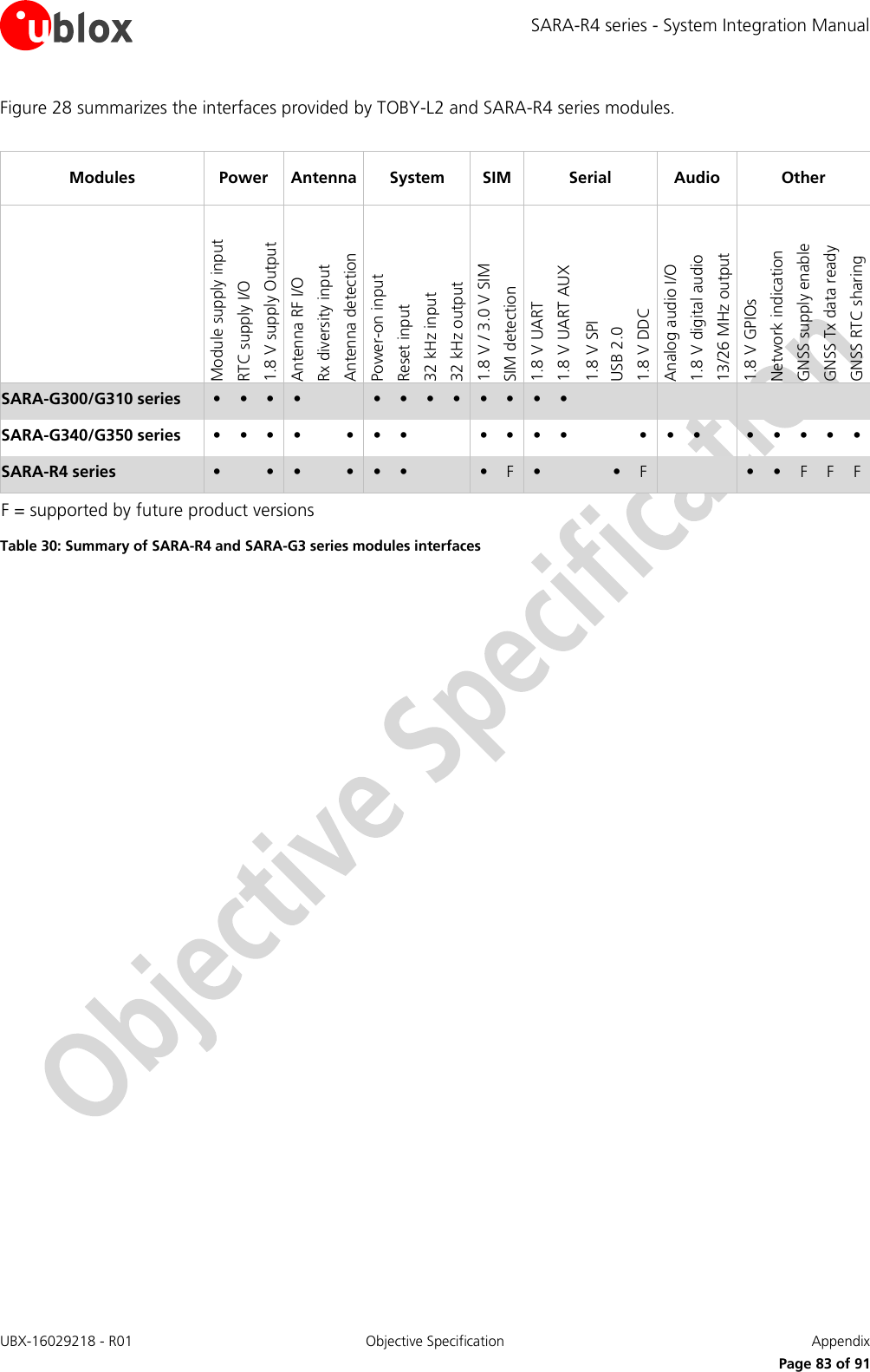
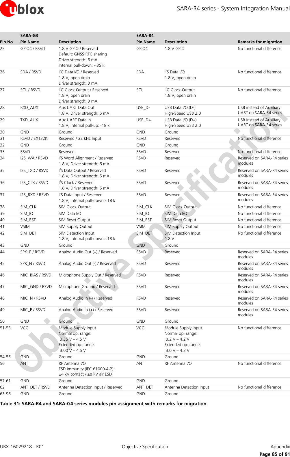
![SARA-R4 series - System Integration Manual UBX-16029218 - R01 Objective Specification Appendix Page 86 of 91 For further details regarding the characteristics, capabilities, usage or settings applicable for each interface of the cellular modules, see the SARA-R4 series Data Sheet [1], the SARA-G3 series Data Sheet [24], the SARA-G3 / SARA-U2 series System Integration Manual [25], the u-blox SARA-R404M AT Commands Manual [1] and the Nested Design Application Note [26]. A.3 Schematic for SARA-R4 and SARA-G3 integration Figure 43 shows an example of schematic diagram where a SARA-R3 or a SARA-G3 series module can be integrated into the same application board, using all the available interfaces and functions of the modules. The different mounting options for the external parts are highlighted in different colors as described in the legend, according to the interfaces supported by the relative modules. TXDRXDRTSCTSDTRDSRRIDCDGND12 TXD9DTR13 RXD10 RTS11 CTS6DSR7RI8DCDGND3V8GND330µF 10nF100nF 56pFSARA-R4 / SARA-G352 VCC53 VCC51 VCC+100µF2V_BCKPGND GNDGNDRTC back-up1.8V UART DTE1.8V UART DTE16 RSVD / GPIO13V8Network Indicator18 RESET_NApplication ProcessorOpen Drain Output15 PWR_ON100kOpen Drain OutputTXDRXD29 TXD_AUX / USB_D+28 RXD_AUX / USB_D-0Ω0ΩTPTP15pF33 RSVDV_BCKPTPTP47pFSIM Card ConnectorCCVCC (C1)CCVPP (C6)CCIO (C7)CCCLK (C3)CCRST (C2)GND (C5)47pF 47pF 100nF41VSIM39SIM_IO38SIM_CLK40SIM_RST47pFSW1 SW24V_INT42SIM_DET470k ESD ESD ESD ESD ESD ESD56ANT62ANT_DET10k 82nH33pF Connector27pF ESDExternal Antenna1kTPu-blox 1.8V GNSS Receiver4.7kOUTINGNDLDO RegulatorSHDNRSVD / SDARSVD / SCL4.7k3V8 1V8_GPSSDA2SCL232K_OUT / GPIO3RSVD / GPIO4TxD1EXTINT02627242547kVCCRSVD / GPIO2 23V_INTBCLKLRCLK10µF1µFAudio Codec MAX9860SDINSDOUTSDASCL36RSVD / I2S_CLK34RSVD / I2S_WA35RSVD / I2S_TXD37RSVD / I2S_RXD19RSVD / CODEC_CLK MCLKIRQn10k100nFVDDSpeakerOUTPOUTNMicrophoneMICBIAS 1µF 2.2k1µF1µFMICLNMICLPMICGND2.2kESD ESDV_INTEMIEMI27pF27pFEMIEMIESD ESD27pF27pF31EXT32K / RSVD0Ω49RSVD / MIC_P2.2k2.2k 2.2k48RSVD / MIC_N2.2k10uF46RSVD / MIC_BIAS47RSVD / MIC_GND100nF100nF44RSVD / SPK_P45RSVD / SPK_NV_INTVBUSD+D-GND17 RSVD / VUSB_DETGNDUSB 2.0 Host0Ω0Ω0Ω0Ω0ΩTPTPTP0Ωfor SARA-G300 / SARA-G310Mount for SARA-G300 / SARA-G310 modulesMount for SARA-G340 / SARA-G350 modulesMount for SARA-R4 modulesMount for SARA-G3 modulesMount for SARA-G340 / SARA-G350 / SARA-R4 modulesMount for SARA-G3 and SARA-R4 modulesLEGEND+0Ω0Ω0ΩTPTP15pF39nH0Ωfor SARA-G3 modules0ΩTPTP 0Ω0Ω0ΩTPTP0ΩTP Figure 43: Example of complete schematic diagram to integrate SARA-R4 modules and SARA-G3 modules on the same application board, using all the available interfaces / functions of the modules](https://usermanual.wiki/u-blox/2AGQN1NNN/User-Guide-3327358-Page-86.png)
![SARA-R4 series - System Integration Manual UBX-16029218 - R01 Objective Specification Related documents Page 89 of 91 Related documents [1] u-blox SARA-R404M AT Commands Manual, Docu No UBX-17003787 [2] u-blox EVK-R2xx User Guide, Docu No UBX-16016088 [3] u-blox Windows Embedded OS USB Driver Installation Application Note, Docu No UBX-14003263 [4] Universal Serial Bus Revision 2.0 specification, http://www.usb.org/developers/docs/usb20_docs/ [5] ITU-T Recommendation V.24 - 02-2000 - List of definitions for interchange circuits between Data Terminal Equipment (DTE) and Data Circuit-terminating Equipment (DCE), http://www.itu.int/rec/T-REC-V.24-200002-I/en [6] 3GPP TS 27.007 - AT command set for User Equipment (UE) [7] 3GPP TS 27.005 - Use of Data Terminal Equipment - Data Circuit terminating; Equipment (DTE - DCE) interface for Short Message Service (SMS) and Cell Broadcast Service (CBS) [8] 3GPP TS 27.010 - Terminal Equipment to User Equipment (TE-UE) multiplexer protocol [9] u-blox Mux Implementation Application Note, Docu No UBX-13001887 [10] I2C-bus specification and user manual - Rev. 5 - 9 October 2012 - NXP Semiconductors, http://www.nxp.com/documents/user_manual/UM10204.pdf [11] u-blox GNSS Implementation Application Note, Docu No UBX-13001849 [12] GSM Association TS.09 - Battery Life Measurement and Current Consumption Technique http://www.gsma.com/newsroom/wp-content/uploads//TS.09_v8.0.pdf [13] CENELEC EN 61000-4-2 (2001): "Electromagnetic compatibility (EMC) – Part 4-2: Testing and measurement techniques – Electrostatic discharge immunity test". [14] ETSI EN 301 489-1 V1.8.1: “Electromagnetic compatibility and Radio spectrum Matters (ERM); EMC standard for radio equipment and services; Part 1: Common technical requirements” [15] ETSI EN 301 489-7 V1.3.1 “Electromagnetic compatibility and Radio spectrum Matters (ERM); EMC standard for radio equipment and services; Part 7: Specific conditions for mobile and portable radio and ancillary equipment of digital cellular radio telecommunications systems“ [16] ETSI EN 301 489-24 V1.4.1 "Electromagnetic compatibility and Radio spectrum Matters (ERM); EMC standard for radio equipment and services; Part 24: Specific conditions for IMT-2000 CDMA Direct Spread (UTRA) for Mobile and portable (UE) radio and ancillary equipment" [17] 3GPP TS 51.010-2 - Technical Specification Group GSM/EDGE Radio Access Network; Mobile Station (MS) conformance specification; Part 2: Protocol Implementation Conformance Statement (PICS) [18] 3GPP TS 34.121-2 - Technical Specification Group Radio Access Network; User Equipment (UE) conformance specification; Radio transmission and reception (FDD); Part 2: Implementation Conformance Statement (ICS) [19] 3GPP TS 36.521-1 - Evolved Universal Terrestrial Radio Access; User Equipment conformance specification; Radio transmission and reception; Part 1: Conformance Testing [20] 3GPP TS 36.521-2 - Evolved Universal Terrestrial Radio Access (E-UTRA); User Equipment conformance specification; Radio transmission and reception; Part 2: Implementation Conformance Statement (ICS) [21] 3GPP TS 36.523-2 - Evolved Universal Terrestrial Radio Access (E-UTRA) and Evolved Packet Core (EPC); User Equipment conformance specification; Part 2: Implementation Conformance Statement (ICS) [22] u-blox End user test Application Note, Docu No UBX-13001922 [23] u-blox Package Information Guide, Docu No UBX-14001652 [24] u-blox SARA-G3 series Data Sheet, Docu No UBX-13000993 [25] u-blox SARA-G3 / SARA-U2 series System Integration Manual, Docu No UBX- 13000995 [26] u-blox Nested Design Application Note, Docu No UBX-16007243 Some of the above documents can be downloaded from u-blox web-site (http://www.u-blox.com/).](https://usermanual.wiki/u-blox/2AGQN1NNN/User-Guide-3327358-Page-89.png)