u blox 2AGQN4NNN Cellular Module User Manual SARA R4 N4 series
u-blox AG Cellular Module SARA R4 N4 series
UserManual.wiki
>
u blox
>
2AGQN4NNN User Manual
>
User Manual 1
Contents
1.
User Manual
2.
Users Manual
3.
User Manual 1
4.
User Manual 2
5.
AdhereTech User Manual
User Manual 1
Navigation menu
Upload a User Manual
Namespaces
Wiki Guide
HTML
PDF
Info
Views
User Manual
Discussion / Help
Navigation
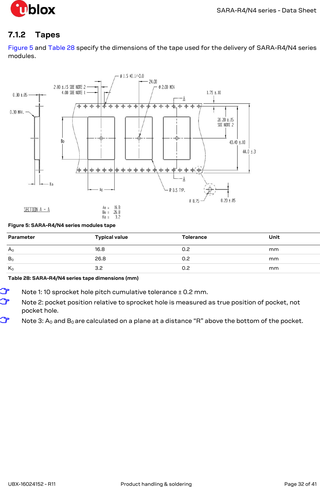
![SARA-R4/N4 series - Data Sheet UBX-16024152 - R11 Functional description Page 8 of 41 Item SARA-R404M SARA-R410M SARA-R412M SARA-N410 Data rate LTE category M1: up to 375 kb/s UL up to 300 kb/s DL LTE category M1: up to 375 kb/s UL up to 300 kb/s DL LTE category NB11: up to 62.5 kb/s UL up to 27.2 kb/s DL LTE category M1: up to 375 kb/s UL up to 300 kb/s DL LTE category NB1: up to 62.5 kb/s UL up to 27.2 kb/s DL GPRS multi-slot class 333: Up to 85.6 kb/s UL Up to 107 kb/s DL EGPRS multi-slot class 333: Up to 236.8 kb/s UL Up to 296.0 kb/s DL LTE category NB1: up to 62.5 kb/s UL up to 27.2 kb/s DL Table 2: SARA-R4/N4 series LTE Cat M1, LTE Cat NB1, EGPRS, GPRS and GSM characteristics 1.5 AT command support The SARA-R4/N4 series modules support AT commands according to the 3GPP standards TS 27.007 [4], TS 27.005 [5], TS 27.010 [6], and the u-blox AT command extension. ☞ For the complete list of all supported AT commands and their syntax, see the SARA-R4/N4 series AT Commands Manual [1]. 3 GPRS/EGPRS multi-slot class 33 implies a maximum of 5 slots in Down-Link and 4 slots in Up-Link with 6 slots in total.](https://usermanual.wiki/u-blox/2AGQN4NNN.User-Manual-1/User-Guide-3940430-Page-8.png)
![SARA-R4/N4 series - Data Sheet UBX-16024152 - R11 Interfaces Page 9 of 41 1.6 Supported features Table 3 lists some of the main features supported by SARA-R4/N4 series modules. For more details, see the SARA-R4/N4 series System Integration Manual [2] and the SARA-R4/N4 series AT Commands Manual [1]. Feature Description Network Indication GPIO configured to indicate the network status: registered home network, registered roaming, data call enabled, no service. The feature can be enabled through the +UGPIOC AT command. Antenna Detection The ANT_DET pin provides antenna presence detection capability, evaluating the resistance from the ANT pin to GND by means of an external antenna detection circuit implemented on the application board. The antenna supervisor (i.e. antenna detection) feature can be enabled through the +UANTR AT command. Embedded TCP and UDP stack Embedded TCP/IP and UDP/IP stack including direct link mode for TCP and UDP sockets. Sockets can be set in Direct Link mode to establish a transparent end-to-end communication with an already connected TCP or UDP socket via the serial interface. FTP File Transfer Protocol functionality is supported via AT commands. HTTP Hyper-Text Transfer Protocol functionality is supported via AT commands. Embedded SSL/TLS 4 With the support of X.509 certificates, embedded SSL/TLS provides server and client authentication, data encryption, data signature and enables TCP/IP applications to communicate over a secured and trusted connection. The feature can be configured and enabled by the +USECMNG and +USECPRF AT commands. MQTT 5 Message Queuing Telemetry Transport is an ISO standard publish-subscribe messaging protocol designed for lightweight M2M communications over TCP. MQTT allows clients to communicate one-to-one, one-to-many and many-to-one over a long-lived outgoing TCP connection. Dual stack IPv4/IPv6 Capability to move between IPv4 and dual stack network infrastructures. IPv4 and IPv6 addresses can be used. Firmware update Over AT commands (FOAT) Firmware module update over AT command interface. The feature can be enabled and configured through the +UFWUPD AT command. Firmware update Over The Air (uFOTA) u-blox firmware module update over the LTE air interface client/server solution using LWM2M. GNSS via modem 5 Full access to u-blox positioning chips and modules is available through a dedicated DDC (I2C) interface. This means that from any host processor, a single serial port can control the SARA-R4/N4 series cellular module and the u-blox positioning chip or module. Power Saving Mode (PSM) The Power Saving Mode (PSM) feature, defined in 3GPP Rel.13, allows further reduction of the module current consumption maximizing the amount of time a device can remain in PSM low power deep sleep mode during periods of data inactivity. It can be activated and configured by the +CPSMS AT command. e-I-DRX 6 Extended Idle mode DRX, based on 3GPP Rel.13, reduces the amount of signaling overhead decreasing the frequency of scheduled measurements and/or transmissions performed by the module in idle mode. This in turn leads to a reduction in the module power consumption while maintaining a perpetual connection with the base station. Coverage Enhancements Mode A Coverage Enhancements Mode A, introduced in 3GPP Rel.13, is used to improve cell signal penetration. Coverage Enhancements Mode B 7 Coverage Enhancements Mode B, introduced in 3GPP Rel.13, is used to further improve cell signal penetration. Table 3: Some of the main features supported by SARA-R4/N4 series modules 2 Interfaces 4 Not supported by “00” product version 5 Not supported by “00” and “01” product versions 6 The feature is disabled on “00” and “01” product versions due to network readiness 7 Not supported by “00”, “01” and “02” product versions](https://usermanual.wiki/u-blox/2AGQN4NNN.User-Manual-1/User-Guide-3940430-Page-9.png)
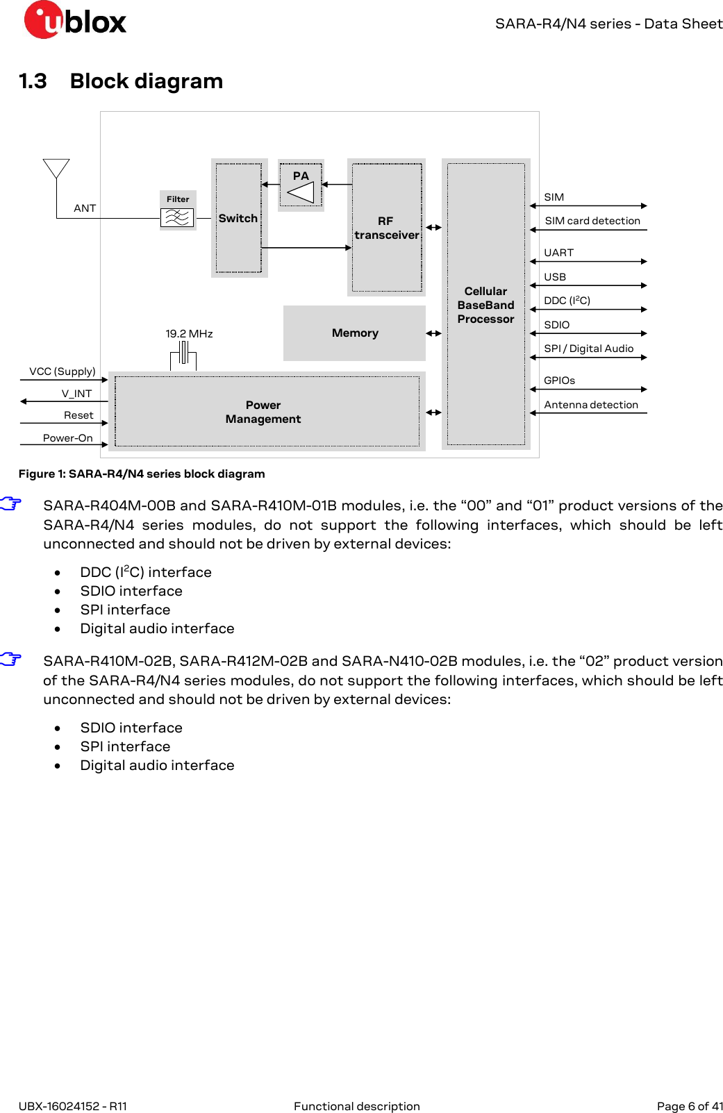
![SARA-R4/N4 series - Data Sheet UBX-16024152 - R11 Interfaces Page 10 of 41 2.1 Power management 2.1.1 Module supply input (VCC) SARA-R4/N4 series modules must be supplied through the VCC pins by a DC power supply. Voltage must be stable, because during operation the current drawn from VCC may vary significantly, based on the power consumption profile of the LTE Cat M1, LTE Cat NB1 and the 2G radio access technologies (described in the SARA-R4/N4 series System Integration Manual [2]). SARA-R412M modules provide separate supply inputs over the three VCC pins: VCC pins #52 and #53 represent the supply input for the internal RF Power Amplifier, demanding most of the total current drawn of the module when RF transmission is enabled during a call VCC pin #51 represents the supply input for the internal baseband Power Management Unit, demanding minor part of the total current drawn of the module when RF transmission is enabled during a call The three VCC pins of SARA-R404M, SARA-R410M and SARA-N410 modules are internally connected to both the internal Power Amplifier and the internal baseband Power Management Unit. It is important that the system power supply circuit is able to withstand the maximum pulse current during a transmit burst at maximum power level (see Table 12). 2.1.2 Generic digital interfaces supply output (V_INT) SARA-R4/N4 series modules provide a 1.8 V supply rail output on the V_INT pin, which is internally generated when the module is switched on. The same voltage domain is used internally to supply the generic digital interfaces of the module. The V_INT supply output can be used in place of an external discrete regulator. 2.2 Antenna interface 2.2.1 Antenna RF interface (ANT) The ANT pin represents the RF antenna interface of the module, with a characteristic impedance of 50 . 2.2.2 Antenna detection (ANT_DET) The ANT_DET pin is an Analog to Digital Converter (ADC) input with a current source provided by SARA-R4/N4 series modules to sense the antenna presence (as an optional feature). It evaluates the resistance from the ANT pin to GND by means of an external antenna detection circuit implemented on the application board (for more details, see the u-blox SARA-R4/N4 series System Integration Manual [2] and the SARA-R4/N4 series AT Commands Manual [1]).](https://usermanual.wiki/u-blox/2AGQN4NNN.User-Manual-1/User-Guide-3940430-Page-10.png)
![SARA-R4/N4 series - Data Sheet UBX-16024152 - R11 Interfaces Page 11 of 41 2.3 System functions 2.3.1 Module power-on SARA-R4/N4 series can be switched on using the following procedure: Low level on the PWR_ON pin, which is normally set high by an internal pull-up, for a valid time period when the applied VCC voltage is within the valid operating range (see sections 4.2.3 and 4.2.8). The PWR_ON line has to be driven by open drain, open collector or contact switch. 2.3.2 Module power-off SARA-R4/N4 series can be properly switched off, with storage of the current parameter settings and a clean network detach, in one of these ways: AT+CPWROFF command (see the SARA-R4/N4 series AT Commands Manual [1]) Low pulse on the PWR_ON pin for a valid time period (see section 4.2.8) An abrupt shutdown occurs on SARA-R4/N4 series modules, without storage of the current parameter settings and without a clean network detach, when: the VCC supply drops below the extended operating range minimum limit a low level is applied on the RESET_N pin, which is normally set high by an internal pull-up, for a valid time period (see section 4.2.9). RESET_N line has to be driven by open drain, open collector or contact switch. 2.3.3 Module reset SARA-R4/N4 series modules can be reset (re-booted) by: AT+CFUN command (see the SARA-R4/N4 series AT Commands Manual [1]). This causes an “internal” or “software” reset of the module. The current parameter settings are saved in the module’s non-volatile memory and a clean network detach is performed. 2.4 SIM 2.4.1 SIM interface A SIM card interface is provided on the VSIM, SIM_IO, SIM_CLK, SIM_RST pins: the high-speed SIM/ME interface is implemented as well as the automatic detection of the required SIM supporting voltage. Both 1.8 V and 3 V SIM types are supported (1.8 V and 3 V). Activation and deactivation with an automatic voltage switch from 1.8 V to 3 V is implemented according to the ISO-IEC 7816-3 specifications. The SIM driver supports the PPS procedure for baud-rate selection, according to the values proposed by the SIM card/chip. 2.4.2 SIM detection The GPIO5 pin of SARA-R4/N4 series modules is a 1.8 V digital input which can be configured as an external interrupt to detect the SIM card presence, as intended to be properly connected to the mechanical switch of an external SIM card holder. For more details, see the SARA-R4/N4 series System Integration Manual [2] and the SARA-R4/N4 series AT Commands Manual [1].](https://usermanual.wiki/u-blox/2AGQN4NNN.User-Manual-1/User-Guide-3940430-Page-11.png)
![SARA-R4/N4 series - Data Sheet UBX-16024152 - R11 Interfaces Page 12 of 41 2.5 Serial communication The SARA-R4/N4 series provides the following serial communication interfaces: UART interface: asynchronous serial interface available for the communication with a DTE host application processor (AT commands, data communication, FW update by means of FOAT) USB interface: High-Speed USB 2.0 compliant interface available for communications with a USB host application processor (AT commands, data communication, FW update by means of the FOAT feature), for FW update by means of the u-blox tool and for diagnostics SPI interface: Serial Peripheral Interface available for communications with an external compatible device SDIO interface: Secure Digital Input Output interface available for communications with a compatible device DDC interface: I2C bus compatible interface available for communications with external I2C devices 2.5.1 UART interface SARA-R4/N4 series modules include a 9-wire unbalanced asynchronous serial interface (UART) for communication with an application host processor (AT commands and data communication). ☞ The UART is available only if the USB is not enabled as AT command / data communication interface: UART and USB cannot be concurrently used for this purpose. UART features are: Complete serial port with RS-232 functionality conforming to the ITU-T V.24 Recommendation [9], with CMOS compatible signal levels (0 V for low data bit or ON state and 1.8 V for high data bit or OFF state) Data lines (RXD as output, TXD as input), hardware flow control lines (CTS as output, RTS as input), modem status and control lines (DTR as input, DSR as output, DCD as output, RI as output) are provided The default baud rate is 115200 bit/s The default frame format is 8N1 (8 data bits, no parity, 1 stop bit) ☞ Hardware flow control is not supported by the “00”, “01” and SARA-R410M-02B product versions, but the RTS input line needs to be set low (= ON state) to communicate over the UART interface on the “00” and “01” product versions. The UART serial interface can be conveniently configured through AT commands. For more details, see the SARA-R4/N4 series AT Commands Manual [1] and the SARA-R4/N4 series System Integration Manual [2]. Multiplexer protocol SARA-R4/N4 series modules include multiplexer functionality as per 3GPP TS 27.010 [6] on the UART physical link. This is a data link protocol which uses HDLC-like framing and operates between the module (DCE) and the application processor (DTE), allowing a number of simultaneous sessions over the physical link (UART).](https://usermanual.wiki/u-blox/2AGQN4NNN.User-Manual-1/User-Guide-3940430-Page-12.png)
![SARA-R4/N4 series - Data Sheet UBX-16024152 - R11 Interfaces Page 13 of 41 The following virtual channels are defined: Channel 0: for Multiplexer control Channel 1: for all AT commands, and non-Dial Up Network (non-DUN) data connections. UDP, TCP data socket / data call connections through relevant AT commands. Channel 2: for Dial Up Network (DUN) data connection. It requires the host to have and use its own TCP/IP stack. The DUN can be initiated on the modem side or terminal/host side. Channel 3: for u-blox GNSS data tunneling (not supported by the “00” and “01” product versions). 2.5.2 USB interface SARA-R4/N4 series modules include a high-speed USB 2.0 compliant interface with a maximum 480 Mbit/s data rate according to the USB 2.0 specification [10] representing the main interface for transferring high speed data with a host application processor. The module itself acts as a USB device and can be connected to any USB host equipped with compatible drivers. The USB is the most suitable interface for transferring high speed data between SARA-R4/N4 series and a host processor, available for AT commands, data communication, FW upgrade by means of the FOAT feature, FW upgrade by means of the u-blox dedicated tool and for diagnostic purposes. The USB_D+ / USB_D- lines carry the USB data and signaling, while the VUSB_DET pin represents the input to enable the USB interface by applying an external valid USB VBUS supply voltage (5.0 V typical). ☞ The USB interface is available as an AT command / data communication interface only if an external valid USB VBUS supply voltage (5.0 V typical) is applied at the VUSB_DET input of the module since the switch-on of the module, and then held during normal operations. In this case, the UART will not be available. ☞ If the USB interface is enabled, the module does not enter the low power deep sleep mode: the external USB VBUS supply voltage needs to be removed from the VUSB_DET input of the module to let it enter the Power Saving Mode defined in 3GPP Rel.13. SARA-R4/N4 series modules provide by default a set of two USB functions: AT commands and data communication Diagnostic log For more details regarding USB configurations / capabilities, see the SARA-R4/N4 series System Integration Manual [2]. 2.5.3 SPI interface ☞ The SPI interface is not supported by the “00”, “01” and “02” product versions. SARA-R4/N4 series modules include a Serial Peripheral Interface for communications with compatible external device. The SPI interface can be made available as an alternative function, in a mutually exclusive way, over the digital audio interface pins (I2S_WA / SPI_MOSI, I2S_RXD / SPI_MISO, I2S_CLK / SPI_CLK, I2S_TXD / SPI_CS).](https://usermanual.wiki/u-blox/2AGQN4NNN.User-Manual-1/User-Guide-3940430-Page-13.png)
![SARA-R4/N4 series - Data Sheet UBX-16024152 - R11 Interfaces Page 14 of 41 2.5.4 SDIO interface ☞ The SDIO interface is not supported by the “00”, “01” and “02” product versions. SARA-R4/N4 series modules include a 4-bit Secure Digital Input Output interface (SDIO_D0, SDIO_D1, SDIO_D2, SDIO_D3, SDIO_CLK, and SDIO_CMD) designed to communicate with external compatible SDIO devices. 2.5.5 DDC (I2C) interface ☞ The DDC (I2C) interface is not supported by the “00” and “01” product versions. SARA-R4/N4 series modules include an I2C-bus compatible DDC interface (SDA, SCL) available to communicate with a u-blox GNSS receiver and with external I2C devices as an audio codec: the SARA-R4/N4 series module acts as an I2C master that can communicate with I2C slaves in accordance with the I2C bus specifications [11]. The SDA and SCL pins have internal pull-up to V_INT, so there is no need of additional pull-up resistors on the external application board. 2.6 Audio ☞ Audio is not supported by the “00”, “01” and “02” product versions. SARA-R4/N4 series modules support VoLTE (Voice over LTE Cat M1 radio bearer) for providing audio services. SARA-R4/N4 series modules include an I2S digital audio interface to transfer digital audio data to/from an external compatible audio device. The digital audio interface can be made available as an alternative function, in a mutually exclusive way, over the SPI interface pins (I2S_WA / SPI_MOSI, I2S_RXD / SPI_MISO, I2S_CLK / SPI_CLK, I2S_TXD / SPI_CS).](https://usermanual.wiki/u-blox/2AGQN4NNN.User-Manual-1/User-Guide-3940430-Page-14.png)
![SARA-R4/N4 series - Data Sheet UBX-16024152 - R11 Interfaces Page 15 of 41 2.7 GPIO SARA-R4/N4 series modules include six pins (GPIO1-GPIO6) that can be configured as general purpose input/output or to provide custom functions as summarized in Table 4 (for further details, see the SARA-R4/N4 series System Integration Manual [2] and the GPIO section of the SARA-R4/N4 series AT Commands Manual [1]). Function Description Default GPIO Configurable GPIOs Network status indication Network status: registered / data transmission, no service -- GPIO1 GNSS supply enable 8 Enable/disable the supply of a u-blox GNSS receiver connected to the cellular module by the DDC (I2C) interface -- GPIO2 GNSS data ready 8 Sense when a u-blox GNSS receiver connected to the module is ready for sending data by the DDC (I2C) interface -- GPIO3 SIM card detection SIM card physical presence detection -- GPIO5 Module status indication Module switched off or in PSM low power deep sleep mode, versus active or connected mode -- GPIO1, GPIO2, GPIO3, GPIO4, GPIO5, GPIO6 General purpose input Input to sense high or low digital level -- GPIO1, GPIO2, GPIO3, GPIO4, GPIO5, GPIO6 General purpose output Output to set the high or the low digital level -- GPIO1, GPIO2, GPIO3, GPIO4, GPIO6 Pin disabled Tri-state with an internal active pull-down enabled GPIO1, GPIO2, GPIO3, GPIO4, GPIO5, GPIO6 GPIO1, GPIO2, GPIO3, GPIO4, GPIO5, GPIO6 Table 4: GPIO custom functions configuration 8 Not supported by “00” and “01” product versions](https://usermanual.wiki/u-blox/2AGQN4NNN.User-Manual-1/User-Guide-3940430-Page-15.png)
![SARA-R4/N4 series - Data Sheet UBX-16024152 - R11 Pin definition Page 18 of 41 No Name Power domain I/O Description Remarks 27 SCL DDC O I2C bus clock line Fixed open drain. Internal 2.2 k pull-up resistor to V_INT. Not supported by “00” and “01” product versions See section 4.2.13 for detailed electrical specs. 28 USB_D- USB I/O USB Data Line D- 90 nominal differential impedance. Pull-up, pull-down and series resistors, as required by the USB 2.0 specifications [10], are part of the USB pin driver and shall not be provided externally. See section 4.2.11 for detailed electrical specs. Provide test point for diagnostic purposes. 29 USB_D+ USB I/O USB Data Line D+ 90 nominal differential impedance. Pull-up, pull-down and series resistors, as required by USB 2.0 specifications [10], are part of the USB pin driver and shall not be provided externally. See section 4.2.11 for detailed electrical specs. Provide test point for diagnostic purposes. 30 GND - N/A Ground All the GND pins must be connected to ground 31 RSVD - N/A RESERVED pin Leave unconnected. 32 GND - N/A Ground All the GND pins must be connected to ground 33 RSVD - N/A RESERVED pin This pin can be connected to GND. 34 I2S_WA / SPI_MOSI GDI O / O I2S word alignment / SPI Master Output Slave Input I2S word alignment, alternatively configurable as SPI Master Output Slave Input Not supported by “00”, “01” and “02” product versions See section 4.2.12 for detailed electrical specs. 35 I2S_TXD / SPI_CS GDI O / O I2S transmit data / SPI Chip Select I2S transmit data out, alternatively configurable as SPI Chip Select Not supported by “00”, “01” and “02” product versions See section 4.2.12 for detailed electrical specs. 36 I2S_CLK / SPI_CLK GDI O / O I2S clock / SPI clock I2S clock, alternatively configurable as SPI clock Not supported by “00”, “01” and “02” product versions See section 4.2.12 for detailed electrical specs. 37 I2S_RXD / SPI_MISO GDI I / I I2S receive data / SPI Master Input Slave Output I2S receive data input, alternatively configurable as SPI Master Input Slave Output Not supported by “00”, “01” and “02” product versions See section 4.2.12 for detailed electrical specs. 38 SIM_CLK SIM O SIM clock See section 4.2.10 for detailed electrical specs. 39 SIM_IO SIM I/O SIM data Internal 4.7 k pull-up resistor to VSIM. See section 4.2.10 for detailed electrical specs. 40 SIM_RST SIM O SIM reset See section 4.2.10 for detailed electrical specs. 41 VSIM - O SIM supply output VSIM = 1.80 V typical or 2.95 V typical generated by the module according to the external SIM card type. See section 4.2.3 for detailed electrical specs. 42 GPIO5 GDI I SIM detection SIM card presence detection input, alternatively configurable as GPIO (see section 2.7). See section 4.2.12 for detailed electrical specs. 43 GND - N/A Ground All the GND pins must be connected to ground 44 SDIO_D2 GDI I/O SDIO serial data [2] Not supported by “00”, “01” and “02” product versions See section 4.2.12 for detailed electrical specs. 45 SDIO_CLK GDI O SDIO serial clock Not supported by “00”, “01” and “02” product versions See section 4.2.12 for detailed electrical specs. 46 SDIO_CMD GDI I/O SDIO command Not supported by “00”, “01” and “02” product versions See section 4.2.12 for detailed electrical specs.](https://usermanual.wiki/u-blox/2AGQN4NNN.User-Manual-1/User-Guide-3940430-Page-18.png)
![SARA-R4/N4 series - Data Sheet UBX-16024152 - R11 Pin definition Page 19 of 41 No Name Power domain I/O Description Remarks 47 SDIO_D0 GDI I/O SDIO serial data [0] Not supported by “00”, “01” and “02” product versions See section 4.2.12 for detailed electrical specs. 48 SDIO_D3 GDI I/O SDIO serial data [3] Not supported by “00”, “01” and “02” product versions See section 4.2.12 for detailed electrical specs. 49 SDIO_D1 GDI I/O SDIO serial data [1] Not supported by “00”, “01” and “02” product versions See section 4.2.12 for detailed electrical specs. 50 GND - N/A Ground All the GND pins must be connected to ground 51 VCC - I Module supply input All VCC pins must be connected to external supply. SARA-R404M, SARA-R410M and SARA-N410: supply input for all internal parts. SARA-R412M: supply input for internal BB PMU. See section 4.2.3 and 4.2.4 for detailed specs. 52 VCC - I Module supply input All VCC pins must be connected to external supply. SARA-R404M, SARA-R410M and SARA-N410: supply input for all internal parts. SARA-R412M: supply input for internal RF PA. See section 4.2.3 and 4.2.4 for detailed specs. 53 VCC - I Module supply input All VCC pins must be connected to external supply. SARA-R404M, SARA-R410M and SARA-N410: supply input for all internal parts. SARA-R412M: supply input for internal RF PA. See section 4.2.3 and 4.2.4 for detailed specs. 54 GND - N/A Ground All the GND pins must be connected to ground 55 GND - N/A Ground All the GND pins must be connected to ground 56 ANT - I/O RF input/output 50 nominal impedance. See section 4.2.5 for detailed electrical specs. 57 GND - N/A Ground All the GND pins must be connected to ground 58 GND - N/A Ground All the GND pins must be connected to ground 59 GND - N/A Ground All the GND pins must be connected to ground 60 GND - N/A Ground All the GND pins must be connected to ground 61 GND - N/A Ground All the GND pins must be connected to ground 62 ANT_DET ADC I Antenna detection Antenna presence detection function. See section 4.2.7 for detailed electrical specs. 63 GND - N/A Ground All the GND pins must be connected to ground 64 GND - N/A Ground All the GND pins must be connected to ground 65-96 GND - N/A Ground All the GND pins must be connected to ground Table 5: SARA-R4/N4 series pin-out ☞ For more information about the pin-out, see the u-blox SARA-R4/N4 series System Integration Manual [2]. ☞ See Appendix A for an explanation of the abbreviations and terms used.](https://usermanual.wiki/u-blox/2AGQN4NNN.User-Manual-1/User-Guide-3940430-Page-19.png)
![SARA-R4/N4 series - Data Sheet UBX-16024152 - R11 Electrical specifications Page 24 of 41 4.2.5 LTE RF characteristics The LTE bands supported by SARA-R4/N4 series modules are defined in Table 2, while the following Table 13 describes the Transmitting and Receiving frequencies according to 3GPP TS 36.521-1 [7]. Parameter Min. Max. Unit Remarks Frequency range FDD Band 12 (700 MHz) Uplink 699 716 MHz Module transmit Downlink 729 746 MHz Module receive Frequency range FDD Band 17 (700 MHz) Uplink 704 716 MHz Module transmit Downlink 734 746 MHz Module receive Frequency range FDD Band 28 (700 MHz) Uplink 703 748 MHz Module transmit Downlink 758 803 MHz Module receive Frequency range FDD Band 13 (700 MHz) Uplink 777 787 MHz Module transmit Downlink 746 756 MHz Module receive Frequency range FDD Band 20 (800 MHz) Uplink 832 862 MHz Module transmit Downlink 791 821 MHz Module receive Frequency range FDD Band 26 (850 MHz) Uplink 814 849 MHz Module transmit Downlink 859 894 MHz Module receive Frequency range FDD Band 18 (850 MHz) Uplink 815 830 MHz Module transmit Downlink 860 875 MHz Module receive Frequency range FDD Band 5 (850 MHz) Uplink 824 849 MHz Module transmit Downlink 869 894 MHz Module receive Frequency range FDD Band 19 (850 MHz) Uplink 830 845 MHz Module transmit Downlink 875 890 MHz Module receive Frequency range FDD Band 8 (900 MHz) Uplink 880 915 MHz Module transmit Downlink 925 960 MHz Module receive Frequency range FDD Band 4 (1700 MHz) Uplink 1710 1755 MHz Module transmit Downlink 2110 2155 MHz Module receive Frequency range FDD Band 3 (1800 MHz) Uplink 1710 1785 MHz Module transmit Downlink 1805 1880 MHz Module receive Frequency range FDD Band 2 (1900 MHz) Uplink 1850 1910 MHz Module transmit Downlink 1930 1990 MHz Module receive Frequency range FDD Band 25 (1900 MHz) Uplink 1850 1915 MHz Module transmit Downlink 1930 1995 MHz Module receive Frequency range TDD Band 39 (1900 MHz)14 Uplink 1880 1920 MHz Module transmit Downlink 1880 1920 MHz Module receive Frequency range FDD Band 1 (2100 MHz) Uplink 1920 1980 MHz Module transmit Downlink 2110 2170 MHz Module receive Table 13: LTE operating RF frequency bands SARA-R4/N4 series modules include a UE Power Class 3 LTE Cat M1 / NB1 transmitter (see Table 2), with output power and characteristics according to 3GPP TS 36.521-1 [7]. SARA-R4/N4 series modules LTE receiver characteristics are compliant to 3GPP TS 36.521-1 [7], with LTE conducted receiver sensitivity performance described in Table 14 and Table 15. 14 Supported in LTE category M1 only](https://usermanual.wiki/u-blox/2AGQN4NNN.User-Manual-1/User-Guide-3940430-Page-24.png)
![SARA-R4/N4 series - Data Sheet UBX-16024152 - R11 Electrical specifications Page 25 of 41 Parameter Min. Typical Max. Unit Remarks Receiver input sensitivity Band 12 / 17 (700 MHz) –107.0 dBm Without repetitions Receiver input sensitivity Band 28 (700 MHz) –105.0 dBm Without repetitions Receiver input sensitivity Band 13 (700 MHz) –105.0 dBm Without repetitions Receiver input sensitivity Band 20 (800 MHz) –105.0 dBm Without repetitions Receiver input sensitivity Band 5 / 18 / 19 / 26 (850 MHz) –105.5 dBm Without repetitions Receiver input sensitivity Band 8 (900 MHz) –106.5 dBm Without repetitions Receiver input sensitivity Band 4 (1700 MHz) –107.5 dBm Without repetitions Receiver input sensitivity Band 3 (1800 MHz) –106.0 dBm Without repetitions Receiver input sensitivity Band 2 / 25 (1900 MHz) –106.0 dBm Without repetitions Receiver input sensitivity Band 1 (2100 MHz) –107.5 dBm Without repetitions Condition: 50 source, throughput > 95%, QPSK modulation, other settings as per 3GPP TS 36.521-1 [7] Table 14: LTE Cat M1 receiver sensitivity performance Parameter Min. Typical Max. Unit Remarks Receiver input sensitivity Band 12 / 17 (700 MHz) –113.5 dBm Without repetitions Receiver input sensitivity Band 28 (700 MHz) –112.0 dBm Without repetitions Receiver input sensitivity Band 13 (700 MHz) –112.0 dBm Without repetitions Receiver input sensitivity Band 20 (800 MHz) –112.0 dBm Without repetitions Receiver input sensitivity Band 5 / 18 / 19 / 26 (850 MHz) –112.5 dBm Without repetitions Receiver input sensitivity Band 8 (900 MHz) –113.0 dBm Without repetitions Receiver input sensitivity Band 4 (1700 MHz) –114.0 dBm Without repetitions Receiver input sensitivity Band 3 (1800 MHz) –113.0 dBm Without repetitions Receiver input sensitivity Band 2 / 25 (1900 MHz) –113.0 dBm Without repetitions Receiver input sensitivity Band 1 (2100 MHz) –114.0 dBm Without repetitions Condition: 50 source, throughput > 95%, other settings as per 3GPP TS 36.521-1 [7] Table 15: LTE Cat NB1 receiver sensitivity performance](https://usermanual.wiki/u-blox/2AGQN4NNN.User-Manual-1/User-Guide-3940430-Page-25.png)
![SARA-R4/N4 series - Data Sheet UBX-16024152 - R11 Electrical specifications Page 26 of 41 4.2.6 2G RF characteristics The 2G bands supported by SARA-R4/N4 series modules are defined in Table 2, while the following Table 16 describes the Transmitting and Receiving frequencies according to 3GPP TS 51.010-1 [8]. Parameter Min Max Unit Remarks Frequency range GSM 850 Uplink 824 849 MHz Module transmit Downlink 869 894 MHz Module receive Frequency range E-GSM 900 Uplink 880 915 MHz Module transmit Downlink 925 960 MHz Module receive Frequency range DCS 1800 Uplink 1710 1785 MHz Module transmit Downlink 1805 1880 MHz Module receive Frequency range PCS 1900 Uplink 1850 1910 MHz Module transmit Downlink 1930 1990 MHz Module receive Table 16: 2G operating RF frequency bands SARA-R4/N4 series modules include a GMSK Power Class 4 transmitter for GSM 850 and E-GSM 900 bands, a GMSK Power Class 1 transmitter for DCS 1800 and PCS 1900 bands, a 8-PSK Power Class E2 transmitter for all 2G bands (see Table 2), with output power and characteristics according to 3GPP TS 51.010-1 [8]. SARA-R4/N4 series modules 2G receiver characteristics are compliant to 3GPP TS 51.010-1 [8], with conducted receiver sensitivity performance described in Table 17. Parameter Min Typical Max Unit Remarks Receiver input sensitivity GSM 850 -109 dBm Downlink RF level @ BER Class II < 2.4 % Receiver input sensitivity E-GSM 900 -109 dBm Downlink RF level @ BER Class II < 2.4 % Receiver input sensitivity DCS 1800 -109 dBm Downlink RF level @ BER Class II < 2.4 % Receiver input sensitivity PCS 1900 -109 dBm Downlink RF level @ BER Class II < 2.4 % Condition: 50 source Table 17: 2G receiver sensitivity performance 4.2.7 ANT_DET pin characteristics Pin Name Parameter Min. Typ. Max. Unit Remarks ANT_DET Output DC current pulse value 35 µA Output DC current pulse time length 1160 µs Table 18: ANT_DET pin characteristics](https://usermanual.wiki/u-blox/2AGQN4NNN.User-Manual-1/User-Guide-3940430-Page-26.png)
![SARA-R4/N4 series - Data Sheet UBX-16024152 - R11 Electrical specifications Page 28 of 41 4.2.11 USB pins USB data lines (USB_D+/ USB_D–) are compliant to the USB 2.0 high-speed specification. See the Universal Serial Bus Revision 2.0 specification [10] for detailed electrical characteristics. Parameter Min. Typical Max. Unit Remarks USB detection voltage on pin VUSB_DET 4.40 5.00 5.25 V High-speed squelch detection threshold (input differential signal amplitude) 100 150 mV High speed disconnect detection threshold (input differential signal amplitude) 525 625 mV High-speed data signaling input common mode voltage range -50 500 mV High-speed idle output level -10 10 mV High-speed data signaling output high level 360 440 mV High-speed data signaling output low level -10 10 mV Chirp J level (output differential voltage) 700 1100 mV Chirp K level (output differential voltage) -900 -500 mV Table 22: USB pin characteristics 4.2.12 Generic Digital Interfaces pins Parameter Min Typical Max Unit Remarks Internal supply for GDI domain 1.80 V Digital I/O Interfaces supply (V_INT) Low-level input -0.30 0.00 0.63 V High-level input 1.17 1.80 2.10 V Low-level output 0.00 0.45 V Max value at IOL = +2.0 mA High-level output 1.35 1.80 V Min value at IOH = –2.0 mA Input leakage current -1 1 µA VIN =0 V or VIN =1.8V Internal pull-up / pull-down resistance 55 390 k Table 23: GDI pin characteristics 4.2.13 DDC (I2C) pins DDC (I2C) lines (SCL and SDA) are compliant to the I2C-bus standard mode specification. See the I2C-Bus Specification [11] for detailed electrical characteristics. Parameter Min Typical Max Unit Remarks Internal supply for GDI domain 1.80 V Digital I/O Interfaces supply (V_INT) Low-level input -0.30 0.00 0.63 V High-level input 1.17 1.80 2.10 V Low-level output 0.00 0.45 V Max value at IOL = +2.0 mA Internal pull-up resistance 2.2 k Input/output leakage current -1 1 µA VIN =0 V or VIN =1.8V Clock frequency on SCL 100 kHz Table 24: DDC (I2C) pin characteristics](https://usermanual.wiki/u-blox/2AGQN4NNN.User-Manual-1/User-Guide-3940430-Page-28.png)
![SARA-R4/N4 series - Data Sheet UBX-16024152 - R11 Mechanical specifications Page 29 of 41 5 Mechanical specifications CRRPQKM1 M1 M2EGH1J1H2J2J2 H2EANT pinBPin 1 IndicatorKGH1 J1AD DOOLNLIFF Figure 3: SARA-R4/N4 series dimensions (bottom and side views) Parameter Description Typical Tolerance A Module Height [mm] 26.0 (1023.6 mil) +0.20/-0.20 (+7.9/-7.9 mil) B Module Width [mm] 16.0 (629.9 mil) +0.20/-0.20 (+7.9/-7.9 mil) C Module Thickness [mm] 2.53 (99.5 mil) +0.25/-0.15 (+9.8/-5.9 mil) D Horizontal Edge to Lateral Pin Pitch [mm] 2.0 (78.7 mil) +0.20/-0.20 (+7.9/-7.9 mil) E Vertical Edge to Lateral Pin Pitch [mm] 2.5 (98.4 mil) +0.20/-0.20 (+7.9/-7.9 mil) F Edge to Lateral Pin Pitch [mm] 1.05 (41.3 mil) +0.20/-0.20 (+7.9/-7.9 mil) G Lateral Pin to Pin Pitch [mm] 1.1 (43.3 mil) +0.02/-0.02 (+0.8/-0.8 mil) H1 Lateral Pin Height [mm] 0.8 (31.5 mil) +0.02/-0.02 (+0.8/-0.8 mil) H2 Lateral Pin close to ANT Height [mm] 0.9 (35.4 mil) +0.02/-0.02 (+0.8/-0.8 mil) I Lateral Pin Width [mm] 1.5 (59.1 mil) +0.02/-0.02 (+0.8/-0.8 mil) J1 Lateral Pin to Pin Distance [mm] 0.3 (11.8 mil) +0.02/-0.02 (+0.8/-0.8 mil) J2 Lateral Pin to Pin close to ANT Distance [mm] 0.2 (7.9 mil) +0.02/-0.02 (+0.8/-0.8 mil) K Horizontal Edge to Central Pin Pitch [mm] 2.75 (108.3 mil) +0.20/-0.20 (+7.9/-7.9 mil) L Vertical Edge to Central Pin Pitch [mm] 2.75 (108.3 mil) +0.20/-0.20 (+7.9/-7.9 mil) M1 Central Pin to Pin Horizontal Pitch [mm] 1.8 (70.9 mil) +0.02/-0.02 (+0.8/-0.8 mil) M2 Central Pin to Pin Horizontal Pitch [mm] 3.6 (141.7 mil) +0.02/-0.02 (+0.8/-0.8 mil) N Central Pin to Pin Vertical Pitch [mm] 2.1 (82.7 mil) +0.02/-0.02 (+0.8/-0.8 mil) O Central Pin Height and Width [mm] 1.1 (43.3 mil) +0.02/-0.02 (+0.8/-0.8 mil) P Horizontal Edge to Pin 1 Indicator Pitch [mm] 0.9 (35.4 mil) +0.20/-0.20 (+7.9/-7.9 mil) Q Vertical Edge to Pin 1 Indicator Pitch [mm] 1.0 (39.4 mil) +0.20/-0.20 (+7.9/-7.9 mil) R Pin 1 Indicator Height and Width [mm] 0.6 (23.6 mil) +0.02/-0.02 (+0.8/-0.8 mil) Weight Module Weight [g] < 3 Table 25: SARA-R4/N4 series dimensions ☞ The module height tolerance +/–0.20 mm may be exceeded close to the corners of the PCB due to the cutting process: in the worst cases, the height could be +0.40 mm longer than the typical value. ☞ For information regarding Footprint and Paste Mask recommended for the application board integrating the cellular module, see the SARA-R4/N4 series System Integration Manual [2].](https://usermanual.wiki/u-blox/2AGQN4NNN.User-Manual-1/User-Guide-3940430-Page-29.png)
![SARA-R4/N4 series - Data Sheet UBX-16024152 - R11 Qualification and approvals Page 30 of 41 6 Qualification and approvals 6.1 Reliability tests Tests for product family qualifications according to ISO 16750 “Road v–hicles - Environmental conditions and testing for electrical and electronic equipment“, and appropriate standards. 6.1.1 Approvals Products marked with this lead-free symbol on the product label comply w“th the "Directive 2002/95/EC of the European Parliament and the Council on the Restriction of Use of certain Hazardous Substances in Electrical and Electronic E”uipment" (RoHS). SARA-R4/N4 series modules are RoHS compliant. No natural rubbers, hygroscopic materials, or materials containing asbestos are employed. Table 27 summarizes the main approvals for SARA-R4/N4 series modules. Certification SARA-R404M-00B SARA-R410M-01B SARA-R410M-02B SARA-R412M-02B SARA-N410-02B GCF • PTCRB • • • • CE Europe • • FCC US FCC ID • XPY2AGQN1NNN • XPY2AGQN4NNN • XPY2AGQN4NNN • • ISED Canada ISED ID • 8595A-2AGQN4NNN • 8595A-2AGQN4NNN • • IFT Mexico • • RCM Australia • NCC Taiwan • Verizon • • AT&T • • • T-Mobile • • Bell • Telus • Telstra • Table 26: SARA-R4/N4 series main certification approvals summary ☞ For guidelines and notices about compliance with certification approvals requirements integrating the SARA-R4/N4 series modules in the end-device, see the SARA-R4/N4 series System Integration Manual [2]. ☞ For the complete list of approvals and for specific details on all country, conformance and network operators’ certifications, including related certificates of compliancy, please contact the u-blox office or sales representative nearest you.](https://usermanual.wiki/u-blox/2AGQN4NNN.User-Manual-1/User-Guide-3940430-Page-30.png)
![SARA-R4/N4 series - Data Sheet UBX-16024152 - R11 Product handling & soldering Page 31 of 41 7 Product handling & soldering 7.1 Packaging SARA-R4/N4 series modules are delivered as hermetically sealed, reeled tapes to enable efficient production, production lot set-up and tear-down. For more information about packaging, see the u-blox Package Information User Guide [3]. 7.1.1 Reels SARA-R4/N4 series modules are deliverable in quantities of 250 pieces on a reel. The modules are delivered using reel type B2 described in Figure 4 and in the u-blox Package Information Guide [3]. Figure 4: SARA-R4/N4 series modules reel Parameter Specification Reel Type B2 Delivery Quantity 250 Table 27: Reel information for SARA-R4/N4 series modules Quantities of less than 250 pieces are also available. Contact u-blox for more information.](https://usermanual.wiki/u-blox/2AGQN4NNN.User-Manual-1/User-Guide-3940430-Page-31.png)
![SARA-R4/N4 series - Data Sheet UBX-16024152 - R11 Product handling & soldering Page 33 of 41 7.2 Moisture Sensitivity Levels ⚠ SARA-R4/N4 series modules are Moisture Sensitive Devices (MSD) in accordance to the IPC/JEDEC specification. The Moisture Sensitivity Level (MSL) relates to the packaging and handling precautions required. SARA-R4/N4 series modules are rated at MSL level 4. For more information regarding moisture sensitivity levels, labeling, storage and drying, see the u-blox Package Information Guide [3]. ☞ For the MSL standard, see IPC/JEDEC J-STD-020 (can be downloaded from www.jedec.org). 7.3 Reflow soldering Reflow profiles are to be selected according to u-blox recommendations (see the SARA-R4/N4 series System Integration Manual [2]). ⚠ Failure to observe these recommendations can result in severe damage to the device! 7.4 ESD precautions ⚠ SARA-R4/N4 series modules contain highly sensitive electronic circuitry and are Electrostatic Sensitive Devices (ESD). Handling SARA-R4/N4 series modules without proper ESD protection may destroy or damage them permanently. SARA-R4/N4 series modules are Electrostatic Sensitive Devices (ESD) and require special ESD precautions typically applied to ESD sensitive components. Table 7 details the maximum ESD ratings of the SARA-R4/N4 series modules. Proper ESD handling and packaging procedures must be applied throughout the processing, handling and operation of any application that incorporates the SARA-R4/N4 series module. ESD precautions should be implemented on the application board where the module is mounted, as described in the SARA-R4/N4 series System Integration Manual [2]. ⚠ Failure to observe these recommendations can result in severe damage to the device!](https://usermanual.wiki/u-blox/2AGQN4NNN.User-Manual-1/User-Guide-3940430-Page-33.png)
![SARA-R4/N4 series - Data Sheet UBX-16024152 - R11 Related documents Page 39 of 41 Related documents [1] u-blox SARA-R4/N4 series AT Commands Manual, Doc. No. UBX-17003787 [2] u-blox SARA-R4/N4 series System Integration Manual, Doc. No. UBX-16029218 [3] u-blox Package Information User Guide, Doc. No. UBX-14001652 [4] 3GPP TS 27.007 - AT command set for User Equipment (UE) [5] 3GPP TS 27.005 - Use of Data Terminal Equipment - Data Circuit terminating Equipment (DTE - DCE) interface for Short Message Service (SMS) and Cell Broadcast Service (CBS) [6] 3GPP TS 27.010 - Terminal Equipment to User Equipment (TE-UE) multiplexer protocol [7] 3GPP TS 36.521-1 - Evolved Universal Terrestrial Radio Access; User Equipment conformance specification; Radio transmission and reception; Part 1: Conformance Testing [8] 3GPP TS 51.010-1 - Mobile Station conformance specification; Part 1: Conformance specification [9] ITU-T Recommendation V24, 02-2000. List of definitions for interchange circuits between Data Terminal Equipment (DTE) and Data Connection Equipment (DCE) [10] Universal Serial Bus Revision 2.0 specification, www.usb.org/developers/docs/usb20_docs/ [11] I2C-bus specification and user manual - Rev.5- 9 October 2012 - NXP Semiconductors, www.nxp.com/documents/user_manual/UM10204.pdf ☞ For regular updates to u-blox documentation and to receive product change notifications, register on our homepage (www.u-blox.com).](https://usermanual.wiki/u-blox/2AGQN4NNN.User-Manual-1/User-Guide-3940430-Page-39.png)