u blox ANNAB1 Wireless Communication System Module User Manual
u-blox AG Wireless Communication System Module
UserManual.wiki
>
u blox
>
ANNAB1 User Manual
User Manual
Navigation menu
Upload a User Manual
Namespaces
Wiki Guide
HTML
PDF
Info
Views
User Manual
Discussion / Help
Navigation
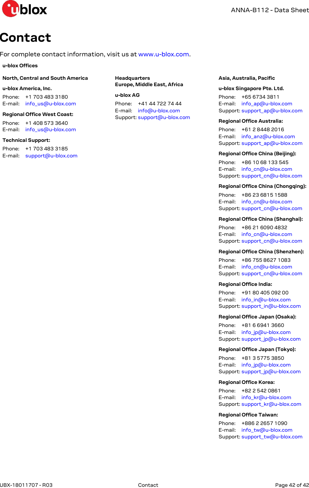
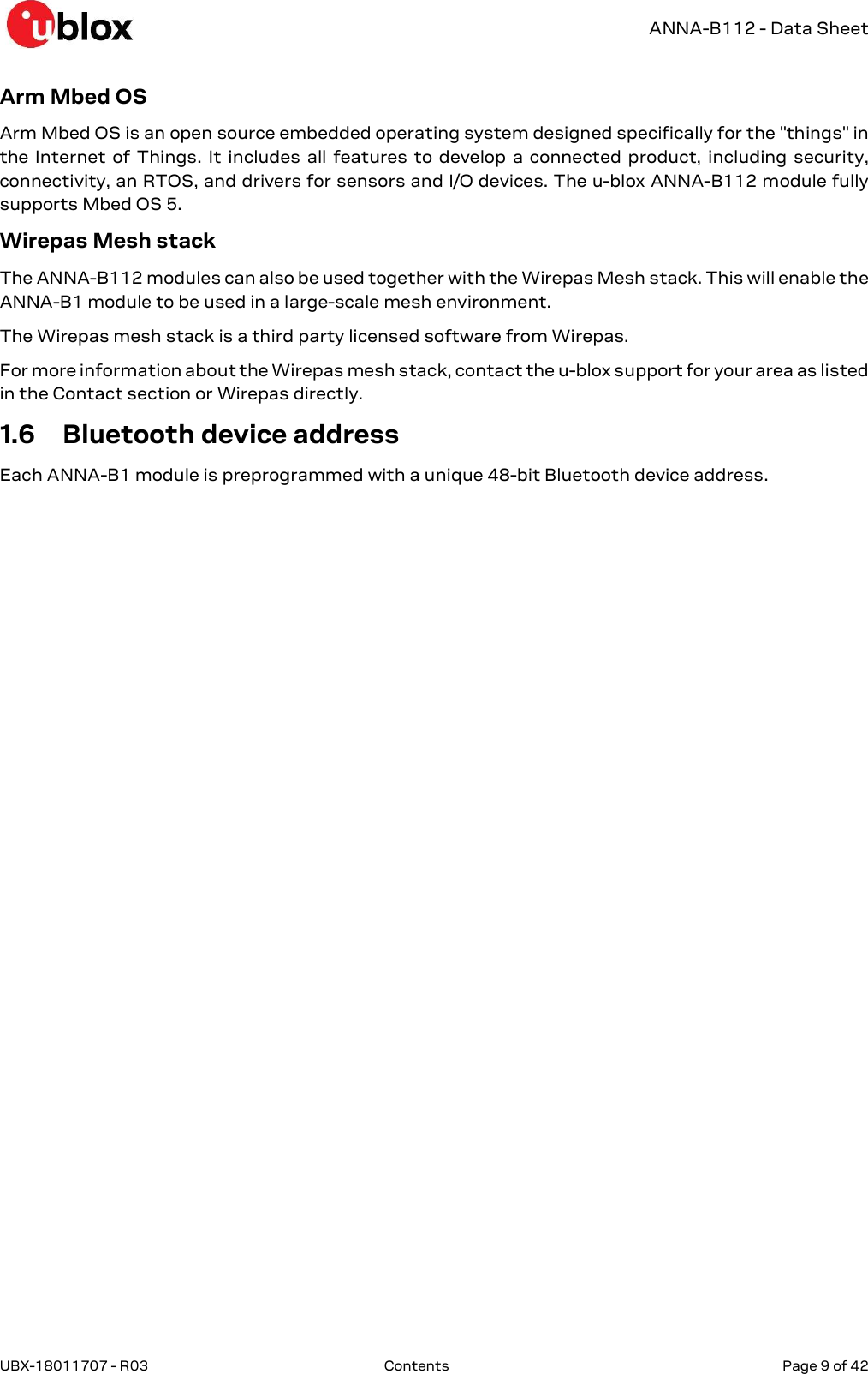
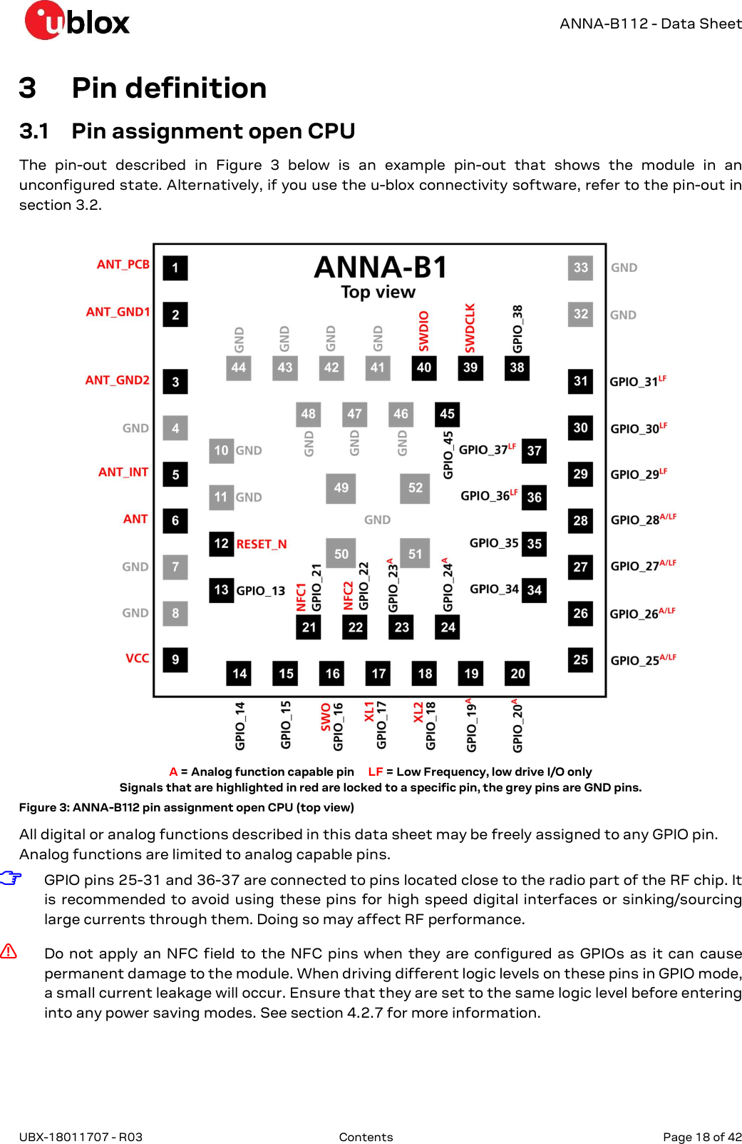
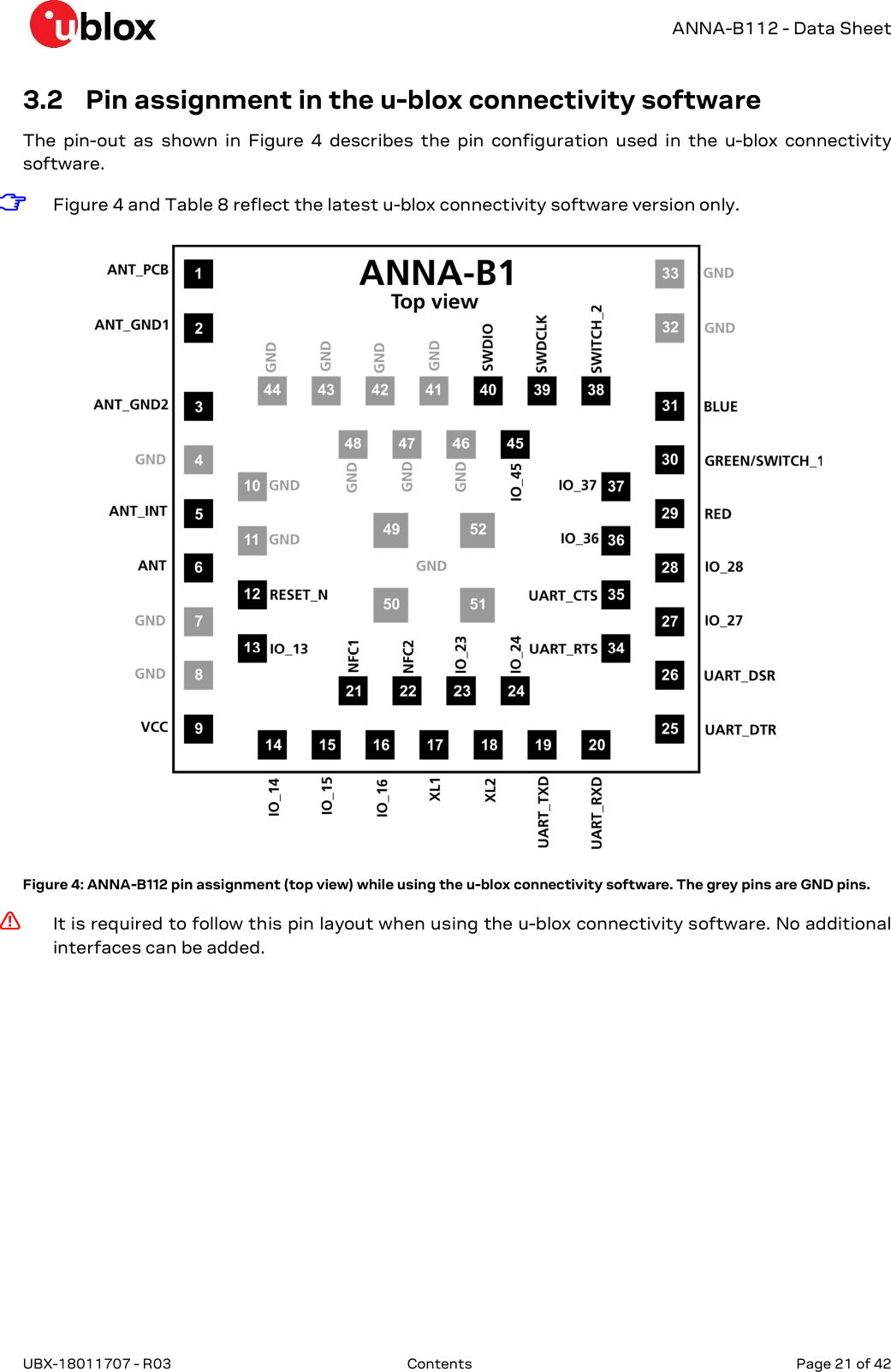
![ANNA-B112 - Data Sheet UBX-18011707 - R03 Contents Page 8 of 42 1.5 Software options The integrated application processor of the ANNA-B112 module is an Arm Cortex-M4 with FPU that has 512 kB flash memory and 64 kB RAM. The software structure of any program running on the module can be broken down into the following components: Radio stack Bootloader (optional) Application ☞ More information on each option can be found in the ANNA-B112 System Integration Manual [1]. 1.5.1 u-blox connectivity software The ANNA-B1 module is preflashed with u-blox connectivity software. The u-blox connectivity software enables the use of the u-blox Low Energy Serial Port Service, controlled by AT commands over the UART interface. You can configure ANNA-B112 modules through u-blox s-center software or by using the AT commands. The s-center evaluation software can be downloaded from the u-blox website and is available free of charge. More information on the features and capabilities of the u-blox Low Energy Serial Port Service and how to use this can be found in the ANNA-B112 Getting Started Guide [3] and the u-blox Short Range AT commands manual [2]. 1.5.2 Open CPU A custom application can be embedded in the ANNA-B112 module. The supported development environments are described below. Nordic SDK The Nordic nRF5 SDK provides a rich and well tested software development environment for nRF52-based devices. It includes a broad selection of drivers, libraries, and example applications. Radio Stack Nordic S132 SoftDevice Figure 2: ANNA-B112 software structure and available software options](https://usermanual.wiki/u-blox/ANNAB1/User-Guide-4025350-Page-8.png)
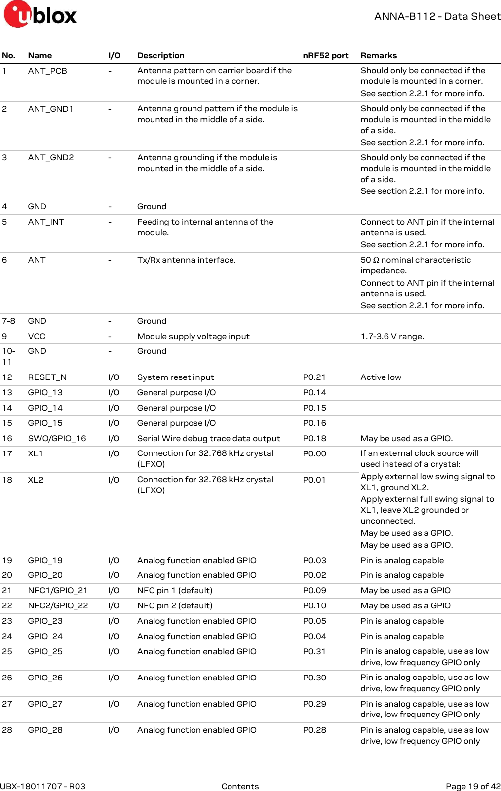
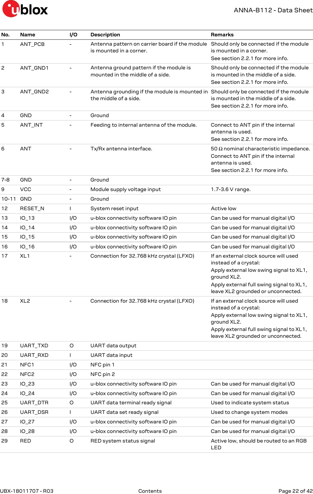
![ANNA-B112 - Data Sheet UBX-18011707 - R03 Contents Page 10 of 42 2 Interfaces 2.1 Power management 2.1.1 Module supply input (VCC) The ANNA-B112 uses an integrated step-down converter to transform the supply voltage presented at the VCC pin into a stable system voltage. Due to this, the ANNA-B112 modules are compatible for use in battery powered designs without the use of an additional voltage converter. You can choose one of the following two on-board voltage converter options: A low-dropout (LDO) converter A DC/DC buck converter Normally, the module will automatically switch between these options depending on the current consumption. Under high loads such as when the radio is active, the DC/DC converter is more efficient, while the LDO converter is more efficient in the power saving modes. 2.2 RF antenna interfaces 2.2.1 2.4 GHz Bluetooth low energy (ANT) The ANNA-B112 2.4 GHz antenna interface can be used in one of the following two ways as mentioned below: 1. With an external antenna or antenna connector: The ANNA-B112 modules provide an antenna pin (ANT) with a nominal characteristic impedance of 50 Ω. This pin can be connected to a carrier board antenna or antenna connector using a controlled impedance trace. See the ANNA-B112 System Integration Manual [1] for more information. OR 2. With the internal antenna: The ANNA-B112 module has an onboard integrated antenna. To use this antenna, the internal antenna pin (ANT_INT) has to be connected directly to the ANT pin (adjacent to the ANT_INT pin). The ANT pins shall not be connected anywhere else in this case and no additional antenna or RF component is needed. Also the connection to the ANT_PCB, ANT_GND1 and ANT_GND2 pins need to be designed correctly see the ANNA-B112 System Integration Manual [1] for more information. 2.2.2 Near Field Communication (NFC) The ANNA-B112 modules include a Near Field Communication interface, capable of operating as a 13.56 MHz NFC tag at a bit rate of 106 kbps. As an NFC tag, data can be read from or written to the ANNA-B112 modules using an NFC reader; however the ANNA-B112 modules are not capable of reading other tags or initiating NFC communications. Two pins are available for connecting to an external NFC antenna: NFC1 and NFC2. See the ANNA-B112 System Integration Manual [1] for more information and NFC antenna design considerations. 2.3 Low Power Oscillator interface During standby mode, the module needs a 32.768 kHz clock source (accuracy +/- 250 ppm). Several clock options are available for the ANNA-B112 module as specified in Table 3: Table 3: Supported low power clock sources for ANNA-B112 Source Current consumption Comment External 32.768kHz crystal 300 nA Connected to the XL1 and XL2 pins (see chapter 3). Internal RC oscillator 620 nA + calibration Needs recalibration every 8 s External 32.768 kHz clock signal - Connected to the XL1 pin (see chapter 3).](https://usermanual.wiki/u-blox/ANNAB1/User-Guide-4025350-Page-10.png)
![ANNA-B112 - Data Sheet UBX-18011707 - R03 Contents Page 11 of 42 See the ANNA-B112 System Integration Manual [1] for more information about connecting an external 32.768 kHz clock source. 2.4 System functions The ANNA-B112 modules are power efficient devices capable of operating in different power saving modes and configurations. Different sections of the module can be powered off when not needed and complex wake up events can be generated from different external and internal inputs. The radio part of the module operates independently from the CPU. The two main power saving modes are: Standby mode Sleep mode Depending on the application, the module should spend most of its time in sleep mode to conserve battery life. 2.4.1 Module power-on ANNA-B112 modules can be switched on in one of the following ways and this will cause the module to reboot: Rising edge on the VCC pin to a valid supply voltage Issuing a reset of the module A wake up event from sleep mode to active mode can be issued by: Changing the state of any digital I/O pin, may be enabled /disabled for each pin. If waking up from standby mode, an event can also be issued by: The on-board Real Time Counter (RTC) A programmable digital or analog sensor event. For example, rising voltage level on an analog comparator pin 2.4.2 Module power-off There is no dedicated pin to power off the ANNA-B112 modules. You can configure any GPIO pin to enter or exit the sleep mode (see section 2.4.4), which essentially powers down the module. An under-voltage (brown-out) shutdown occurs on ANNA-B112 modules when the VCC supply drops below the operating range minimum limit. If this occurs, it is not possible to store the current parameter settings in the module’s non-volatile memory. An over-temperature and under-temperature shutdown can be enabled on ANNA-B112 modules, and is initiated if the temperature measured within the module is outside operating conditions. The temperature is measured by an integrated temperature sensor in the radio chip. For more details see the ANNA-B112 System Integration Manual [1]. 2.4.3 Standby mode Standby mode is one of the power saving modes in ANNA-B112 modules that essentially powers down the module but keeps the system RAM intact and allows for a few low power digital interfaces (including SPI) and analog functions to run continuously. It also allows for complex, autonomous power-up events including periodic RTC events and radio events. The following events can be used to bring the module out of the standby mode: External wake-up events Internal wake-up events from RTC, radio, NFC and so on Analog or digital sensor event (programmable voltage level or edge detection)](https://usermanual.wiki/u-blox/ANNAB1/User-Guide-4025350-Page-11.png)
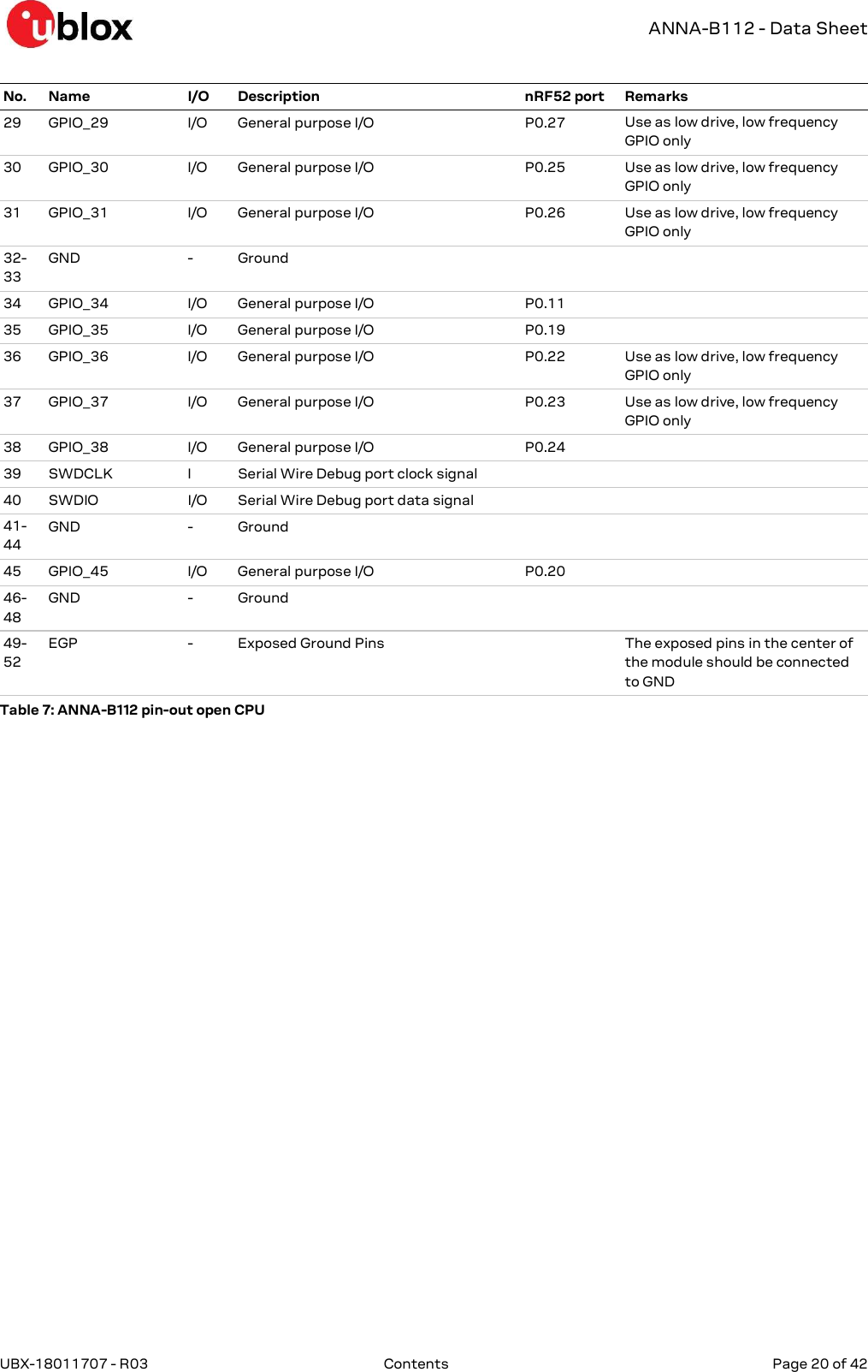
![ANNA-B112 - Data Sheet UBX-18011707 - R03 Contents Page 15 of 42 1x Analog comparator* 1x Low-power analog comparator* *Only one of the comparators can be used simultaneously. 2.7.1 ADC The Analog to Digital Converter (ADC) can sample up to 200 kHz using different inputs as sample triggers. It supports 8/10/12-bit resolution. Any of the 8 analog inputs can be used both as single-ended inputs and as differential pairs for measuring the voltage across them. The ADC supports full 0 V to VCC input range. 2.7.2 Comparator The comparator compares voltages from any analog pin with different references as shown in Table 5. It supports full 0 V to VCC input range and can generate different software events to the rest of the system. 2.7.3 Low power comparator The low-power comparator operates in the same way as the normal comparator, with some reduced functionality. It can be used during sleep mode as a wake up source. 2.7.4 Analog pin options Table 5 shows the supported connections of the analog functions. ☞ An analog pin may not be simultaneously connected to multiple functions. Table 5: Possible uses of analog pin 2.8 u-blox connectivity software features This section describes the available features when using the u-blox connectivity software. For additional information, see the u-blox Short Range AT Commands Manual [2]. 2.8.1 u-blox Serial Port Service (SPS) The serial port service feature enables serial port emulation over Bluetooth low energy. Analog function Can be connected to ADC single-ended input Any analog pin or VCC ADC differential input Any analog pin or VCC pair Comparator IN+ Any analog pin Comparator IN- Pin 19 or 20, VCC, 1.2 V, 1.8 V, 2.4 V Low-power comparator IN+ Any analog pin Low-power comparator IN- Pin 19 or 20, 1/16 to 15/16 VCC in steps of 1/16 VCC](https://usermanual.wiki/u-blox/ANNAB1/User-Guide-4025350-Page-15.png)
![ANNA-B112 - Data Sheet UBX-18011707 - R03 Contents Page 16 of 42 2.8.2 System status signals The RED, GREEN and BLUE pins are used to signal the system status according to Table 6. They are active low and are intended to be routed to an RGB LED. Mode Status RGB LED Color RED GREEN BLUE Data\Extended Data mode (EDM) IDLE Green HIGH LOW HIGH Command mode IDLE Orange LOW LOW HIGH EDM/Data mode, Command mode CONNECTING Purple LOW HIGH LOW EDM/Data mode, Command mode CONNECTED* Blue HIGH HIGH LOW * = LED flashes on data activity Table 6: System status indication ☞ The CONNECTING and CONNECTED statuses indicate u-blox SPS connections. 2.8.3 System control signals The following input signals are used to control the system: RESET_N is used to reset the system. See section 2.4.5 for detailed information. If SWITCH_2 is driven low during start up, the UART serial settings are restored to their default values. SWITCH_2 can be used to open a Bluetooth LE connection with a peripheral device. If both SWITCH_1 and SWITCH_2 are driven low during start up, the system will enter the bootloader mode. If both SWITCH_1 and SWITCH_2 are driven low during start up and held low for 10 seconds, the system will exit the bootloader mode and restore all settings to their factory default. 2.8.4 UART signals In addition to the normal RXD, TXD, CTS, and RTS signals, the u-blox connectivity software adds the DSR and DTR pins to the UART interface. Note that they are not used as originally intended, but to control the state of the ANNA module. For example, depending on the current configuration: The DSR pin can be used to: Enter command mode Disconnect and/or toggle connectable status Enable/disable the rest of the UART interface Enter/wake up from sleep mode The DTR pin can be used to indicate: The system mode If the SPS peers are connected If a Bluetooth LE bonded device is connected A Bluetooth LE GAP connection ☞ See the u-blox Short Range AT Commands Manual [2] for more information. 2.8.5 IO signals When using the u-blox connectivity software, 11 module pins can be used for manual, digital read/write operations. These pins can be configured as outputs or inputs with or without pull-up/pull-down, using AT commands. For more information, see the u-blox Short Range AT Commands Manual [2]. ☞ In this data sheet, these signals are defined as IO signals to distinguish from the GPIO signals described in section 2.6. The IO signals are used with u-blox connectivity software only and](https://usermanual.wiki/u-blox/ANNAB1/User-Guide-4025350-Page-16.png)
![ANNA-B112 - Data Sheet UBX-18011707 - R03 Contents Page 32 of 42 The modular transmitter approval of ANNA-B112 does not exempt the end-product from being evaluated against applicable regulatory demands. The evaluation of the end-product shall be performed with the ANNA-B112 module installed and operating in a way that reflects the intended end-product use case. The upper frequency measurement range of the end product evaluation is the 5th harmonic of 2.4 GHz as declared in 47 CFR Part 15.33 (b)(1). The following requirements apply to all products that integrate a radio module: o Subpart B - UNINTENTIONAL RADIATORS To verify that the composite device of host and module complies with the requirements of FCC part 15B the integrator shall perform sufficient measurements using ANSI 63.4-2014. o Subpart C - INTENTIONAL RADIATORS It is required that the integrator carry out sufficient verification measurements using ANSI 63.10-2013 to validate that the fundamental and out of band emissions of the transmitter part of the composite device complies with the requirements of FCC part 15C. When the items listed above are fulfilled the host manufacturer can use the authorization procedures presented in Table 1 of 47 CFR Part 15.101. 6.3.6.2 Co-location (simultaneous transmission) If the module is to be co-located with another transmitter, additional measurements for simultaneous transmission are required. 6.4 Japan radio equipment compliance 204-810005 Figure 6: Giteki mark, R and the ANNA-B112 MIC certification number For information about compliance of the ANNA-B112 module with the Giteki certification, see the ANNA-B112 System Integration Manual [1]. 6.5 Safety compliance In order to fulfill the safety standard EN 60950-1, the ANNA-B112 modules must be supplied with a Class-2 Limited Power Source.](https://usermanual.wiki/u-blox/ANNAB1/User-Guide-4025350-Page-32.png)
![ANNA-B112 - Data Sheet UBX-18011707 - R03 Contents Page 34 of 42 7 Antennas This chapter gives an overview of the different external antennas that can be used together with the module. ⚠ This radio transmitter IC: 8595A-ANNAB1 has been approved by Industry Canada to operate with the antenna types listed below with the maximum permissible gain and required antenna impedance for each antenna type indicated. Antenna types not included in this list, having a gain greater than the maximum gain indicated for that type, are strictly prohibited for use with this device. ⚠ Cet émetteur radio IC: 8595A-ANNAB1 été approuvé par Industry Canada pour fonctionner avec les types d’antenne énumérés ci-dessous avec le gain maximum autorisé et l’impédance nécessaire pour chaque type d’antenne indiqué. Les types d’antenne ne figurant pas dans cette liste et ayant un gain supérieur au gain maximum indiqué pour ce type-là sont strictement interdits d’utilisation avec cet appareil. 7.1 Approved antennas # Antenna name Manufacturer Comment Gain [dBi] 1 ANNA-B112 internal antenna u-blox See ANNA-B112 System Integration Manual [1] for reference design +0.5 2 PC17.07.0070A Taoglas Patch, PCB, 24 x 11 x 0.8mm, 70 mm cable/U.FL +1 3 FXP75.07.0045B Taoglas Patch, Flexfilm, 5.9 x 4.1 x 0.24 mm, 45 mm cable/U.FL +2.5](https://usermanual.wiki/u-blox/ANNAB1/User-Guide-4025350-Page-34.png)
![ANNA-B112 - Data Sheet UBX-18011707 - R03 Contents Page 37 of 42 8.5 Reflow soldering Reflow profiles are to be selected according to u-blox recommendations. See ANNA-B112 System Integration Manual [1] for more information. ⚠ Failure to observe these recommendations can result in severe damage to the device. 8.6 ESD precautions ⚠ The ANNA-B112 modules contain highly sensitive electronic circuitry and are Electrostatic Sensitive Devices (ESD). Handling the ANNA-B112 modules without proper ESD protection may destroy or damage them permanently. The ANNA-B112 modules are electrostatic sensitive devices (ESD) and require special ESD precautions typically applied to ESD sensitive components. Section 4.1.1 provides the maximum ESD ratings of the ANNA-B112 modules. Proper ESD handling and packaging procedures must be applied throughout the processing, handling and operation of any application that incorporates the ANNA-B112 module. The ESD precautions should be implemented on the application board where the module is mounted as described in the ANNA-B112 System Integration Manual [1]. ⚠ Failure to observe these recommendations can result in severe damage to the device.](https://usermanual.wiki/u-blox/ANNAB1/User-Guide-4025350-Page-37.png)
![ANNA-B112 - Data Sheet UBX-18011707 - R03 Contents Page 39 of 42 Table 23 explains the parts of the product code. Code Meaning Example PPPP Form factor ANNA TG Platform (Technology and Generation) T – Dominant technology, For example, W: Wi-Fi, B: Bluetooth G – Generation B1: Bluetooth Generation 1 VV Variant based on the same platform; range [00…99] 12: default mounting, with internal antenna TT Major Product Version 00: first revision Q Quality grade A: Automotive B: Professional C: Standard B: professional grade XX Minor product version (not relevant for certification) Default value is 00 Table 23: Part identification code 9.3 Ordering information Ordering Code Product ANNA-B112-00B ANNA-B1 module with the option to use either an internal antenna or an external antenna, preflashed with u-blox connectivity software v1.0.0 Table 24: Product ordering codes](https://usermanual.wiki/u-blox/ANNAB1/User-Guide-4025350-Page-39.png)
![ANNA-B112 - Data Sheet UBX-18011707 - R03 Related documents Page 41 of 42 Related documents [1] ANNA-B112 System Integration Manual, document number UBX-18009821 [2] u-blox Short Range AT Commands Manual, document number UBX-14044127 [3] ANNA-B112 Getting Started Guide, document number UBX-18020387 ☞ For regular updates to u-blox documentation and to receive product change notifications, register on our homepage (www.u-blox.com). Revision history Revision Date Name Comments R01 28-Mar-2018 mwej, kgom Initial release. R02 14-May-2018 mwej, kgom Changed the product status to Engineering Sample. Updated main features summary (Table 1) and the block diagram (Figure 1). Updated the countries for modular type approvals (section 1.1 and 6.1). R03 26-Sep-2018 mwej, hekf Changed the distance values in Ch. 6.3.2.1 and Ch. 6.3.2.2. Updated and added missing dimensions in the mechanical drawing (chapter 5). Updated the number of units on a reel in section 8.2. Included information about Approved antennas in section 7.1. Added reference to the ANNA-B112 Getting Started Guide. Updated range figures in Table 1. Updated product marking in section 9.1. Updated the ETSI (Europe), FCC (USA), IC (Canada), Japan certification sections (6.2, 6.3 and 6.4). Updated Tape information in section 8.3.](https://usermanual.wiki/u-blox/ANNAB1/User-Guide-4025350-Page-41.png)