u blox EMMYW163 WLAN/Bluetooth/NFC host-based multiradio module EMMY-W1 User Manual EMMY W1 AntennaReferenceDesign

u-blox AG WLAN/Bluetooth/NFC host-based multiradio module EMMY-W1 EMMY W1 AntennaReferenceDesign

Contents

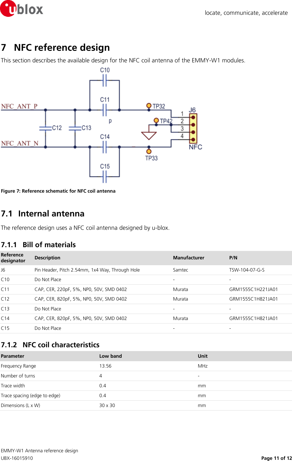
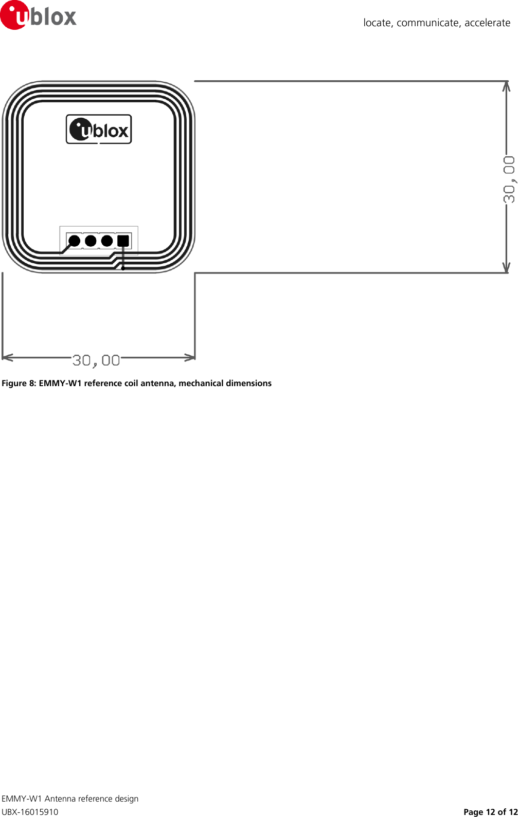
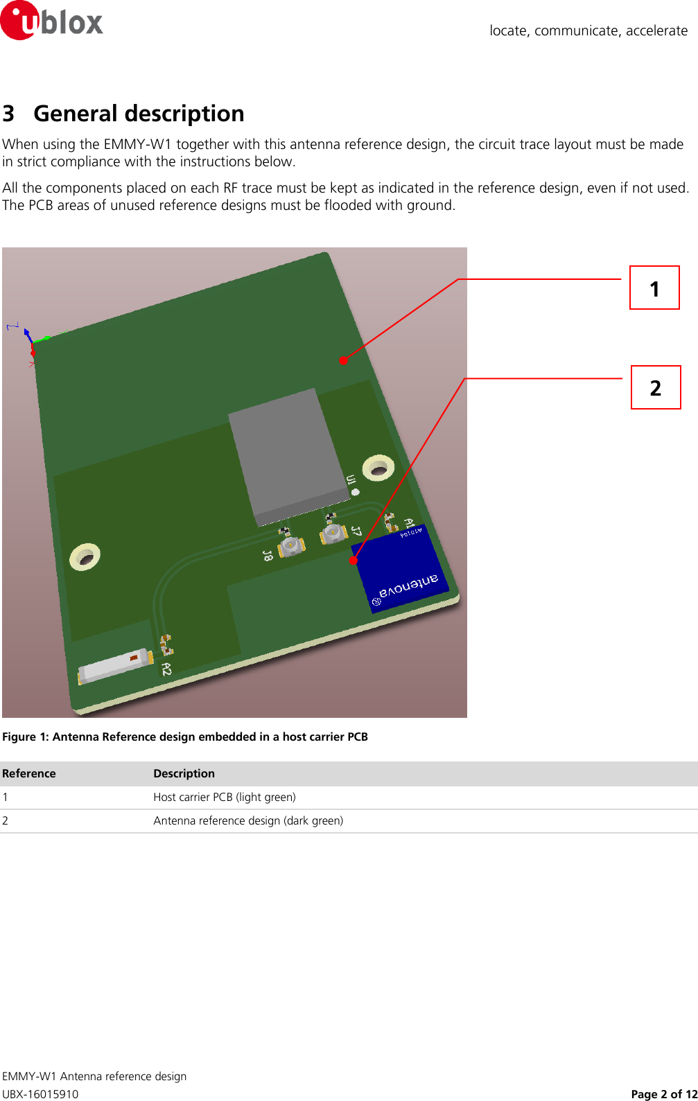
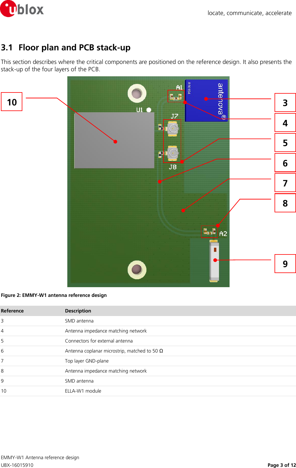
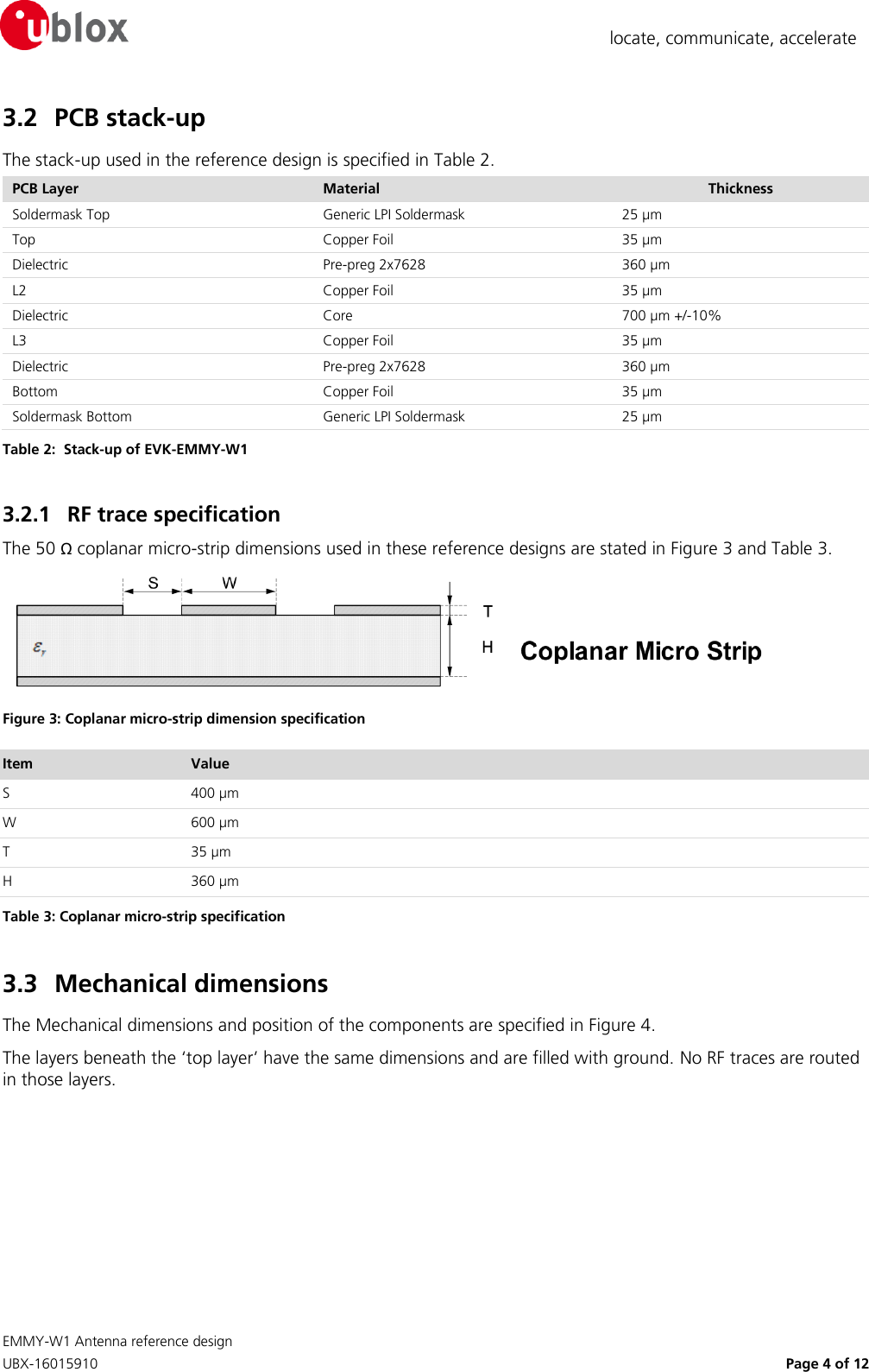
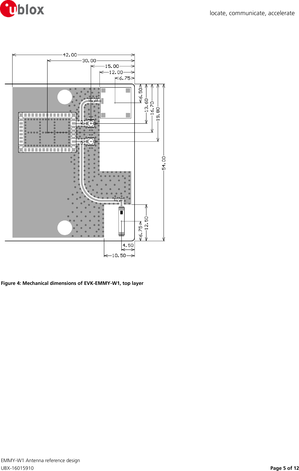
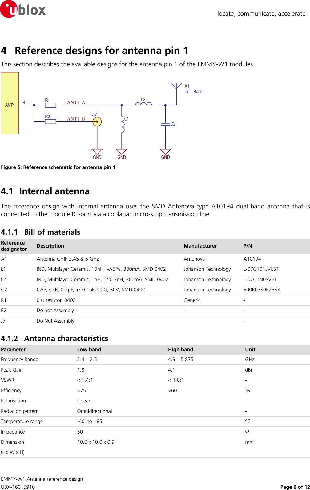
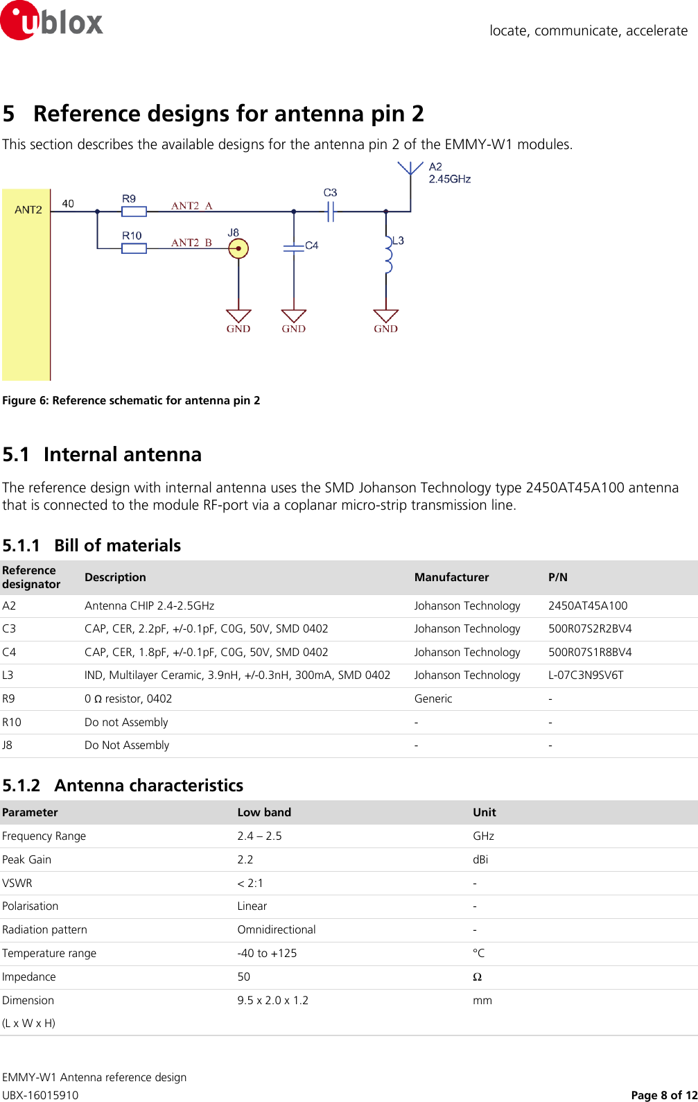
EMMY-W1_AntennaReferenceDesign

 EMMY-W1 Antenna reference design     UBX-16015910    Page 1 of 12  locate, communicate, accelerate EMMY-W1 Antenna reference design Topic : EMMY-W1 Antenna reference design Doc.No: UBX-16015910  Revision R01  Date: Name Signature Created 01-Jul-2016 Stefano Bianconi sbia Checked    Released    We reserve all rights in this document and in the information contained therein. Reproduction, use or disclosure to third parties without express authority is strictly forbidden.  © 2016 u-blox AG 1 Scope This  document  defines  the  essential  specifications  necessary  to  implement  the  EMMY-W1  antenna  reference designs. The information contained herein and its references should be sufficient to guide a skilled person in an attempt  to  implement  the  design  on  a  host  carrier.  It  will  provide  the  designer  with  PCB  layout  details  and expected performance specifications. The document supports the four different PCB designs for Wi-Fi:   Two connector-based designs for the use of external antennas (one for each antenna pin of the module)   Two designs based on SMD antennas (one for each antenna pin of the module) This document also supports general guidelines for the design of the NFC interface. 2 FCC/IC ID reference Model FCC ID IC ID EMMY-W161 XPYEMMYW161 8595A-EMMYW161 EMMY-W163 XPYEMMYW163 8595A-EMMYW163 Table 1: FCC and IC IDs for different models of EMMY-W1 series
 EMMY-W1 Antenna reference design     UBX-16015910    Page 2 of 12  locate, communicate, accelerate 3 General description When using the EMMY-W1 together with this antenna reference design, the circuit trace layout must be made in strict compliance with the instructions below. All the components placed on each RF trace must be kept as indicated in the reference design, even if not used. The PCB areas of unused reference designs must be flooded with ground.   Figure 1: Antenna Reference design embedded in a host carrier PCB Reference Description 1 Host carrier PCB (light green) 2 Antenna reference design (dark green)  2 1
 EMMY-W1 Antenna reference design     UBX-16015910    Page 3 of 12  locate, communicate, accelerate 3.1 Floor plan and PCB stack-up This section describes where the critical components are positioned on the reference design. It also presents the stack-up of the four layers of the PCB.   Figure 2: EMMY-W1 antenna reference design Reference Description 3 SMD antenna 4 Antenna impedance matching network 5 Connectors for external antenna  6 Antenna coplanar microstrip, matched to 50 Ω 7 Top layer GND-plane 8 Antenna impedance matching network 9 SMD antenna 10 ELLA-W1 module   3 6 10 4 5 9 7 8
 EMMY-W1 Antenna reference design     UBX-16015910    Page 4 of 12  locate, communicate, accelerate 3.2 PCB stack-up The stack-up used in the reference design is specified in Table 2. PCB Layer Material Thickness Soldermask Top Generic LPI Soldermask 25 µm Top Copper Foil 35 µm Dielectric Pre-preg 2x7628 360 µm L2 Copper Foil 35 µm Dielectric Core 700 µm +/-10% L3 Copper Foil 35 µm Dielectric Pre-preg 2x7628 360 µm Bottom Copper Foil 35 µm Soldermask Bottom Generic LPI Soldermask 25 µm Table 2:  Stack-up of EVK-EMMY-W1 3.2.1 RF trace specification The 50 Ω coplanar micro-strip dimensions used in these reference designs are stated in Figure 3 and Table 3.  Figure 3: Coplanar micro-strip dimension specification Item Value S 400 µm W 600 µm T 35 µm H 360 µm Table 3: Coplanar micro-strip specification 3.3 Mechanical dimensions The Mechanical dimensions and position of the components are specified in Figure 4. The layers beneath the ‘top layer’ have the same dimensions and are filled with ground. No RF traces are routed in those layers.
 EMMY-W1 Antenna reference design     UBX-16015910    Page 5 of 12  locate, communicate, accelerate  Figure 4: Mechanical dimensions of EVK-EMMY-W1, top layer
 EMMY-W1 Antenna reference design     UBX-16015910    Page 6 of 12  locate, communicate, accelerate 4 Reference designs for antenna pin 1 This section describes the available designs for the antenna pin 1 of the EMMY-W1 modules.  Figure 5: Reference schematic for antenna pin 1 4.1 Internal antenna The  reference  design  with  internal  antenna  uses  the  SMD  Antenova  type  A10194  dual  band  antenna  that  is connected to the module RF-port via a coplanar micro-strip transmission line. 4.1.1 Bill of materials Reference designator Description Manufacturer P/N A1 Antenna CHIP 2.45 & 5 GHz Antenova A10194 L1 IND, Multilayer Ceramic, 10nH, +/-5%, 300mA, SMD 0402 Johanson Technology L-07C10NJV6ST L2 IND, Multilayer Ceramic, 1nH, +/-0.3nH, 300mA, SMD 0402 Johanson Technology L-07C1N0SV6T C2 CAP, CER, 0.2pF, +/-0.1pF, C0G, 50V, SMD 0402 Johanson Technology 500R07S0R2BV4 R1 0 Ω resistor, 0402 Generic - R2 Do not Assembly - - J7 Do Not Assembly - - 4.1.2 Antenna characteristics Parameter Low band High band Unit Frequency Range 2.4 – 2.5  4.9 – 5.875  GHz Peak Gain 1.8 4.1 dBi VSWR < 1.4:1 < 1.8:1 - Efficiency >75 >60 % Polarisation Linear - Radiation pattern Omnidirectional - Temperature range -40  to +85 °C Impedance 50 Ω Dimension (L x W x H) 10.0 x 10.0 x 0.9 mm
 EMMY-W1 Antenna reference design     UBX-16015910    Page 7 of 12  locate, communicate, accelerate 4.2 External antenna The reference design with external antenna uses the micro coaxial connector that is connected to the external antenna via a 50 Ω pigtail. See section 6 for a list of available external antennas. 4.2.1 Bill of materials Reference designator Description Manufacturer P/N A1 Do Not Assembly - - L1 Do Not Assembly - - L2 Do Not Assembly - - C2 Do Not Assembly - - R1 Do Not Assembly - - R2 0 Ω resistor, 0402 Generic - J7 Coaxial Connector, 0 – 6 GHz, SMD Hirose U.FL-R-SMT-1(10)
 EMMY-W1 Antenna reference design     UBX-16015910    Page 8 of 12  locate, communicate, accelerate 5 Reference designs for antenna pin 2 This section describes the available designs for the antenna pin 2 of the EMMY-W1 modules.  Figure 6: Reference schematic for antenna pin 2 5.1 Internal antenna The reference design with internal antenna uses the SMD Johanson Technology type 2450AT45A100 antenna that is connected to the module RF-port via a coplanar micro-strip transmission line.  5.1.1 Bill of materials Reference designator Description Manufacturer P/N A2 Antenna CHIP 2.4-2.5GHz Johanson Technology 2450AT45A100 C3 CAP, CER, 2.2pF, +/-0.1pF, C0G, 50V, SMD 0402 Johanson Technology 500R07S2R2BV4 C4 CAP, CER, 1.8pF, +/-0.1pF, C0G, 50V, SMD 0402 Johanson Technology 500R07S1R8BV4 L3 IND, Multilayer Ceramic, 3.9nH, +/-0.3nH, 300mA, SMD 0402 Johanson Technology L-07C3N9SV6T R9 0 Ω resistor, 0402 Generic - R10 Do not Assembly - - J8 Do Not Assembly - - 5.1.2 Antenna characteristics Parameter Low band Unit Frequency Range 2.4 – 2.5  GHz Peak Gain 2.2 dBi VSWR < 2:1 - Polarisation Linear - Radiation pattern Omnidirectional - Temperature range -40 to +125  °C Impedance 50 Ω Dimension (L x W x H) 9.5 x 2.0 x 1.2 mm
 EMMY-W1 Antenna reference design     UBX-16015910    Page 9 of 12  locate, communicate, accelerate 5.2 External antenna The reference design with external antenna uses the micro coaxial connector that is connected to the external antenna via a 50 Ω pigtail. See section 6 for a list of available external antennas. 5.2.1 Bill of materials Reference designator Description Manufacturer P/N A2 Do not Assembly - - C3 Do Not Assembly - - C4 Do not Assembly - - L3 Do not Assembly - - R9 Do Not Assembly - - R10 0 Ω resistor, 0402 Generic - J8 Coaxial Connector, 0 – 6 GHz, SMD Hirose U.FL-R-SMT-1(10)
 EMMY-W1 Antenna reference design     UBX-16015910    Page 10 of 12  locate, communicate, accelerate 6 Approved external antenna list For Bluetooth operation on EMMY-W163, the module has been tested and approved for use with antennas listed in Table 4. Model name Manufacturer and description Gain [dBi] (peak) ANT-2.4-CW-RCT-RP  Linx, Single-band dipole antenna 2.2 @ 2.4GHz band N/A @ 5GHz band ANT-2.4-CW-RH Linx, Single-band monopole antenna -0.9 GW.26.0151 Taoglas, Single-band dipole antenna 0.0 Table 4: Approved antennas list, single-band operation For Bluetooth and Wi-Fi operations in the 2.4 GHz band and Wi-Fi operation in the 5 GHz band, the module has been tested and approved for use with antennas listed in Table 5. Model name Manufacturer and description Gain [dBi] (peak) ANT-DB1-RAF-RPS  Linx, Dual-band dipole antenna 2.5 @ 2.4GHz band 4.6 @ 5GHz band GW.40.2153 Taoglas, Dual-band dipole antenna 3.74 @ 2.4GHz band 2.5 @ 5GHz band GW.59.3153  Taoglas, Dual-band dipole antenna 2.37 @ 2.4GHz band 2.93 @ 5GHz band RFDPA870900SBLB8G1 Walsin, Dual-band dipole antenna 2 @ 2.4GHz band 3 @ 5GHz band 88395 Delock, Dual-band dipole antenna 1.5 @ 2.4GHz band 2.1 @ 5GHz band Table 5: Approved antennas list, dual-band operation
 EMMY-W1 Antenna reference design     UBX-16015910    Page 11 of 12  locate, communicate, accelerate 7 NFC reference design This section describes the available design for the NFC coil antenna of the EMMY-W1 modules.  Figure 7: Reference schematic for NFC coil antenna 7.1 Internal antenna The reference design uses a NFC coil antenna designed by u-blox. 7.1.1 Bill of materials Reference designator Description Manufacturer P/N J6 Pin Header, Pitch 2.54mm, 1x4 Way, Through Hole Samtec TSW-104-07-G-S C10 Do Not Place - - C11 CAP, CER, 220pF, 5%, NP0, 50V, SMD 0402 Murata GRM1555C1H221JA01 C12 CAP, CER, 820pF, 5%, NP0, 50V, SMD 0402 Murata GRM1555C1H821JA01 C13 Do Not Place - - C14 CAP, CER, 820pF, 5%, NP0, 50V, SMD 0402 Murata GRM1555C1H821JA01 C15 Do Not Place - - 7.1.2 NFC coil characteristics Parameter Low band Unit Frequency Range 13.56 MHz Number of turns 4 - Trace width 0.4 mm Trace spacing (edge to edge) 0.4 mm Dimensions (L x W) 30 x 30 mm
 EMMY-W1 Antenna reference design     UBX-16015910    Page 12 of 12  locate, communicate, accelerate   Figure 8: EMMY-W1 reference coil antenna, mechanical dimensions

Navigation menu