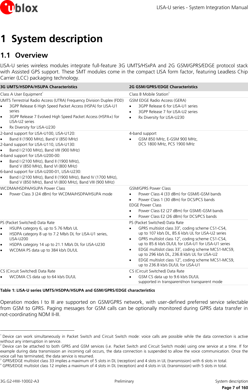
u blox LISAU230 3.75G HSPA Wireless Module User Manual LISA U series
u-blox AG 3.75G HSPA Wireless Module LISA U series
UserManual.wiki
>
u blox
>
LISAU230 User Manual
08 system integration manual
Navigation menu
Upload a User Manual
Namespaces
Wiki Guide
HTML
PDF
Info
Views
User Manual
Discussion / Help
Navigation
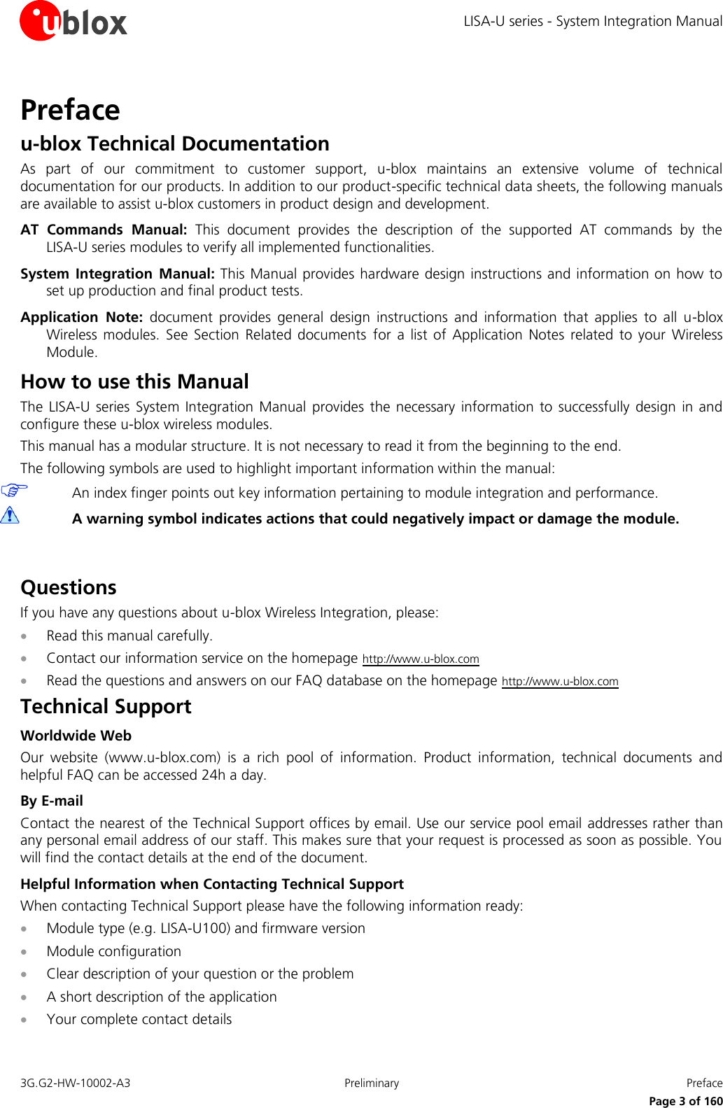
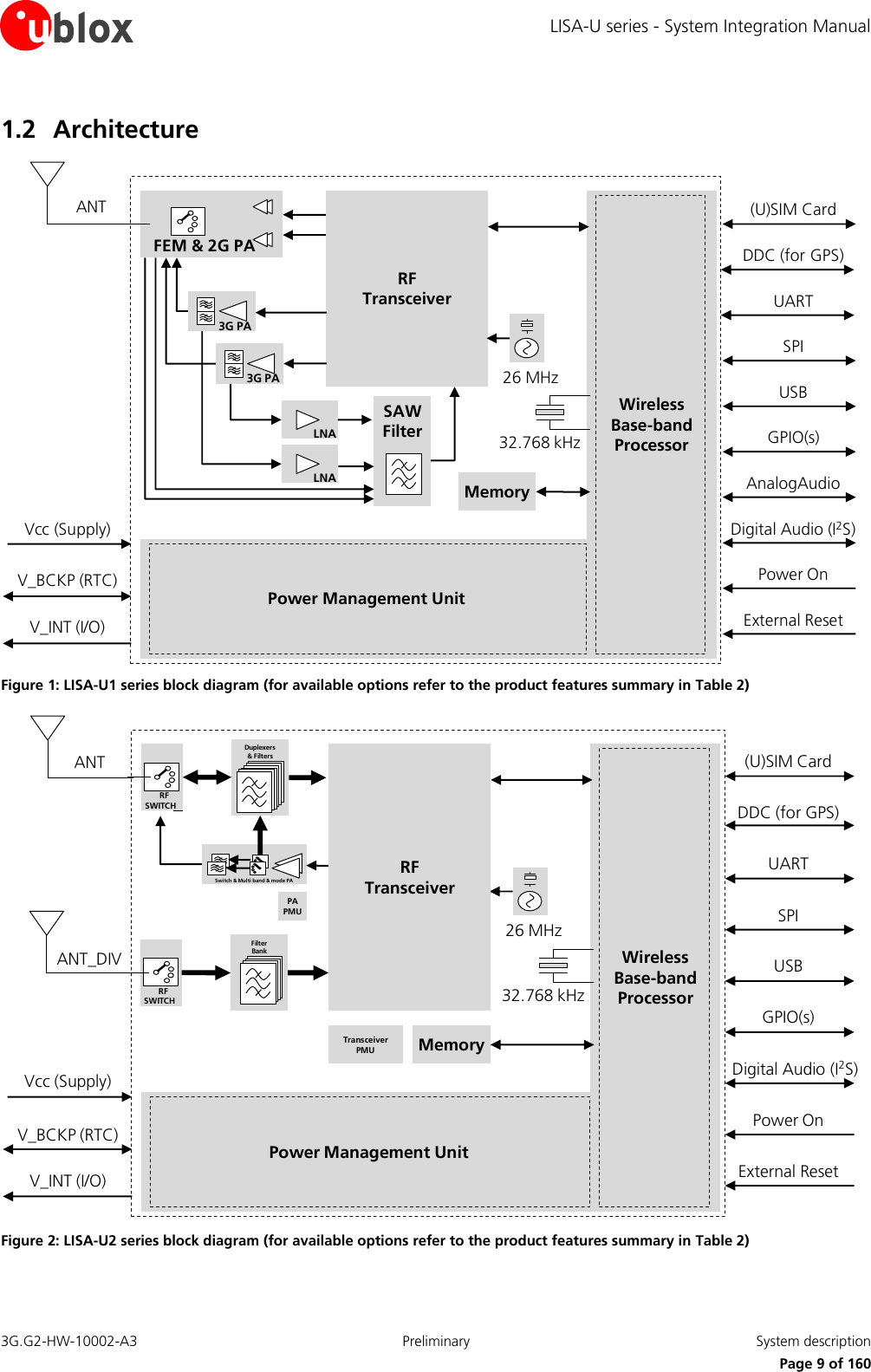
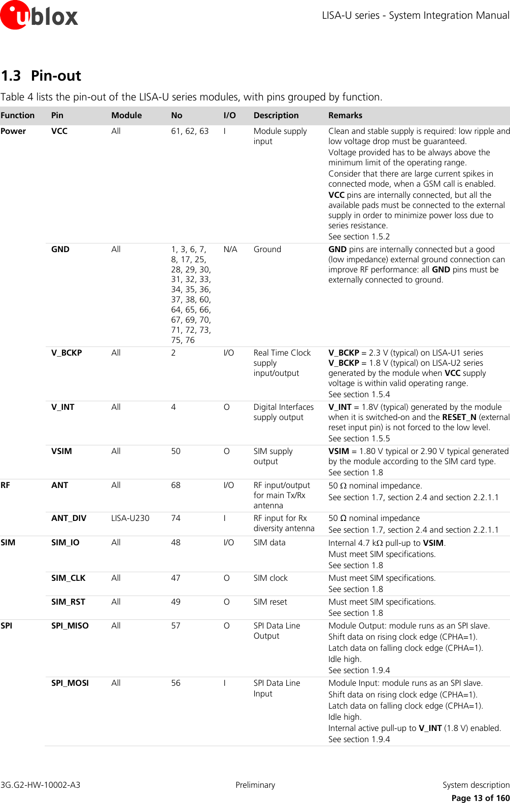
![LISA-U series - System Integration Manual 3G.G2-HW-10002-A3 Preliminary System description Page 8 of 160 Direct Link mode is supported for TCP / UDP sockets except for LISA-U1xx-00 module versions. Regarding 3G transmit and receive data rate capability, LISA-U series modules implement 3G High-Speed Uplink Packet Access (HSUPA) category 6, LISA-U1 series and LISA-U200 modules implement 3G High Speed Downlink Packet Access (HSDPA) category 8, while LISA-U230 modules implement the 3G HSDPA category 14. HSUPA and HSDPA categories determine the maximum speed at which data can be respectively transmitted and received: higher categories allowing faster data transfer rates as indicated in Table 1. The 3G network automatically performs adaptive coding and modulation using a choice of forward error correction code rate and choice of modulation type, to achieve the highest possible data rate and data transmission robustness according to the quality of the radio channel. Regarding 2G transmit and receive data rate capability, LISA-U1 series modules implement GPRS/EGPRS class 12, while LISA-U2 series modules implement GPRS/EGPRS class 33. GPRS and EGPRS classes determine the maximum number of timeslots available for upload and download and thus the speed at which data can be transmitted and received: higher classes typically allowing faster data transfer rates as indicated in Table 1. The 2G network automatically configures the number of timeslots used for reception or transmission (voice calls take precedence over GPRS/EGPRS traffic) and channel encoding (from Coding Scheme 1 up to Modulation and Coding Scheme 9), performing link adaptation to achieve the highest possible data rate. A summary of interfaces and features provided by LISA-U series modules is described in the Table 2. Note that LISA-U130-01 and LISA-U230-01 are available in standard and automotive quality grade versions. Module Technology Bands Interface Audio Functions HSUPA [Mb/s] HSDPA [Mb/s] UMTS/HSPA bands [MHz] GSM/GPRS/EDGE quad-band UART SPI (5 wire) USB DDC for u-blox GPS GPIO Analog Audio Digital Audio Network indication Antenna Supervisor Jamming detection Embedded TCP/UDP stack HTTP, SSL GPS via Modem Embedded AssistNow FW update over AT (FOAT) In-band modem Rx diversity CellLocate SIM Access Profile (SAP) LISA-U100-00 5.76 7.2 850/1900 • 1 1 1 1 5 • • • • • LISA-U100-01 5.76 7.2 850/1900 • 1 1 1 1 5 • • • • • • • • • LISA-U110-00 5.76 7.2 900/2100 • 1 1 1 1 5 • • • • • LISA-U110-01 5.76 7.2 900/2100 • 1 1 1 1 5 • • • • • • • • • LISA-U120-00 5.76 7.2 850/1900 • 1 1 1 1 5 1 1 • • • • • LISA-U120-01 5.76 7.2 850/1900 • 1 1 1 1 5 1 1 • • • • • • • • • LISA-U130-00 5.76 7.2 900/2100 • 1 1 1 1 5 1 1 • • • • • LISA-U130-01 5.76 7.2 900/2100 • 1 1 1 1 5 1 1 • • • • • • • • • • LISA-U200-00 5.76 7.2 800/850/ 1900/2100 • 1 1 1 1 9 • • • • • • LISA-U200-01 5.76 7.2 800/850/900/ 1700/1900/2100 • 1 1 1 1 14 2 • • • • • • • • • • • LISA-U230-01 5.76 21.1 800/850/900/ 1700/1900/2100 • 1 1 1 1 14 2 • • • • • • • • • • • • Table 2: LISA-U series features summary](https://usermanual.wiki/u-blox/LISAU230/User-Guide-1727756-Page-8.png)
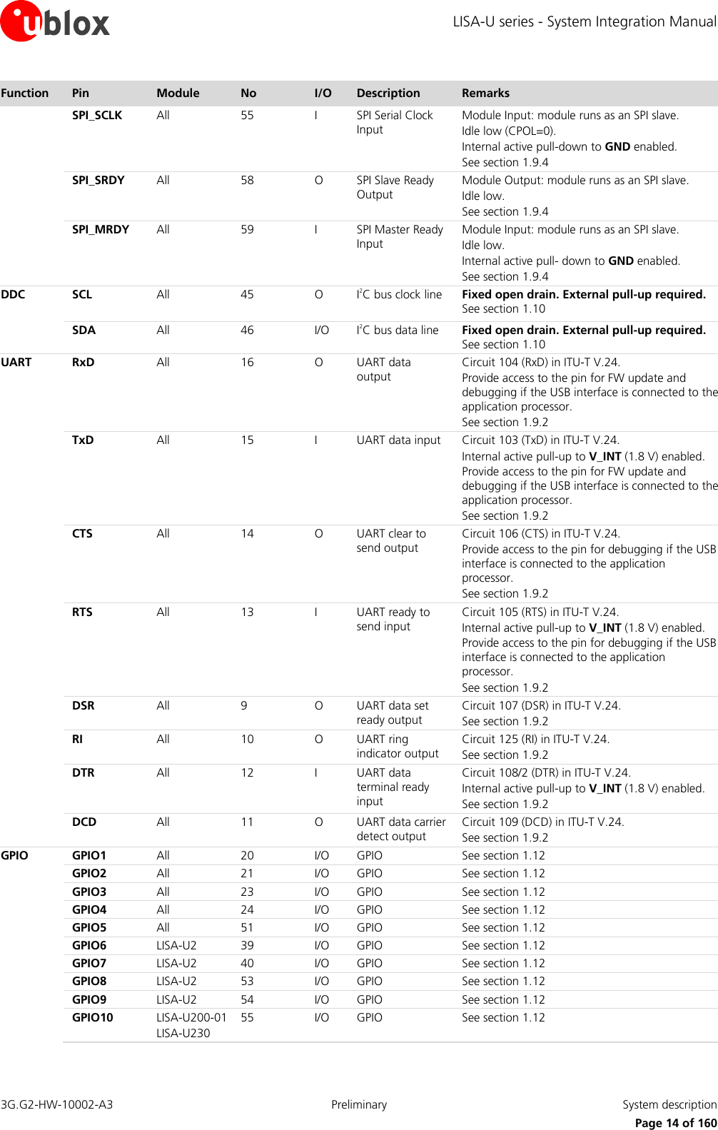
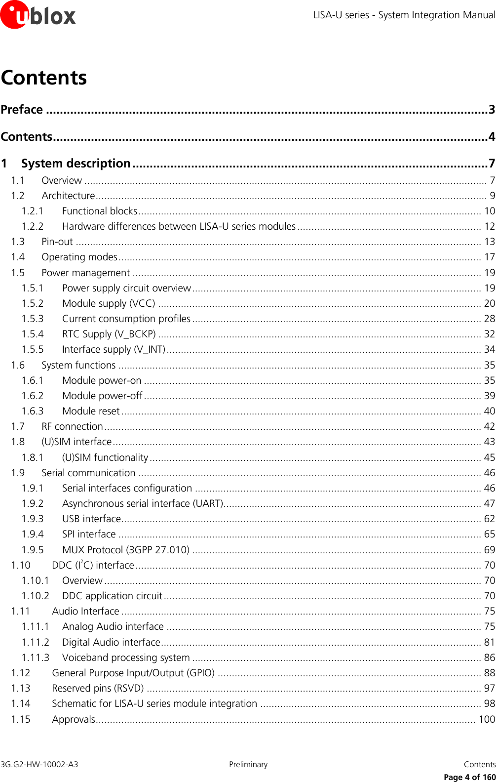
![LISA-U series - System Integration Manual 3G.G2-HW-10002-A3 Preliminary System description Page 15 of 160 Function Pin Module No I/O Description Remarks GPIO11 LISA-U200-01 LISA-U230 56 I/O GPIO See section 1.12 GPIO12 LISA-U200-01 LISA-U230 57 I/O GPIO See section 1.12 GPIO13 LISA-U200-01 LISA-U230 58 I/O GPIO See section 1.12 GPIO14 LISA-U200-01 LISA-U230 59 I/O GPIO See section 1.12 USB VUSB_DET All 18 I USB detect input Input for VBUS (5 V typical) USB supply sense to enable USB interface. Provide access to the pin for FW update and debugging if the USB interface is not connected to the application processor. See section 1.9.3 USB_D- All 26 I/O USB Data Line D- 90 Ω nominal differential impedance Pull-up or pull-down resistors and external series resistors as required by the USB 2.0 high-speed specification [8] are part of the USB pad driver and need not be provided externally. Provide access to the pin for FW update and debugging if the USB interface is not connected to the application processor. See section 1.9.3 USB_D+ All 27 I/O USB Data Line D+ 90 Ω nominal differential impedance Pull-up or pull-down resistors and external series resistors as required by the USB 2.0 high-speed specification [8] are part of the USB pad driver and need not be provided externally. Provide access to the pin for FW update and debugging if the USB interface is not connected to the application processor. See section 1.9.3 System PWR_ON All 19 I Power-on input PWR_ON pin has high input impedance. Do not keep floating in noisy environment: external pull-up required. See section 1.6.1 RESET_N All 22 I External reset input Internal 10 kΩ pull-up to V_BCKP. See section 1.6.3 Analog Audio MIC_N LISA-U120 LISA-U130 39 I Differential analog audio input (negative) Differential analog input shared for all analog path modes: handset, headset, hands-free mode. Internal DC blocking capacitor. See section 1.11.1 MIC_P LISA-U120 LISA-U130 40 I Differential analog audio input (positive) Differential analog input shared for all analog path modes: handset, headset, hands-free mode. Internal DC blocking capacitor. See section 1.11.1 SPK_P LISA-U120 LISA-U130 53 O Differential analog audio output (positive) Differential analog audio output shared for all analog path modes: earpiece, headset and loudspeaker mode. See section 1.11.1 SPK_N LISA-U120 LISA-U130 54 O Differential analog audio output (negative) Differential analog audio output shared for all analog path modes: earpiece, headset and loudspeaker mode. See section 1.11.1 Digital Audio I2S_CLK LISA-U120 LISA-U130 LISA-U200-01 LISA-U230 43 I/O First I2S clock Check device specifications to ensure compatibility to module supported modes. See section 1.11.2.](https://usermanual.wiki/u-blox/LISAU230/User-Guide-1727756-Page-15.png)
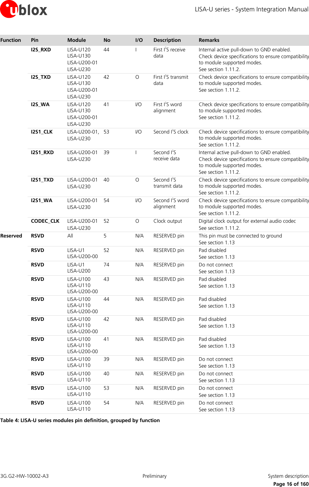
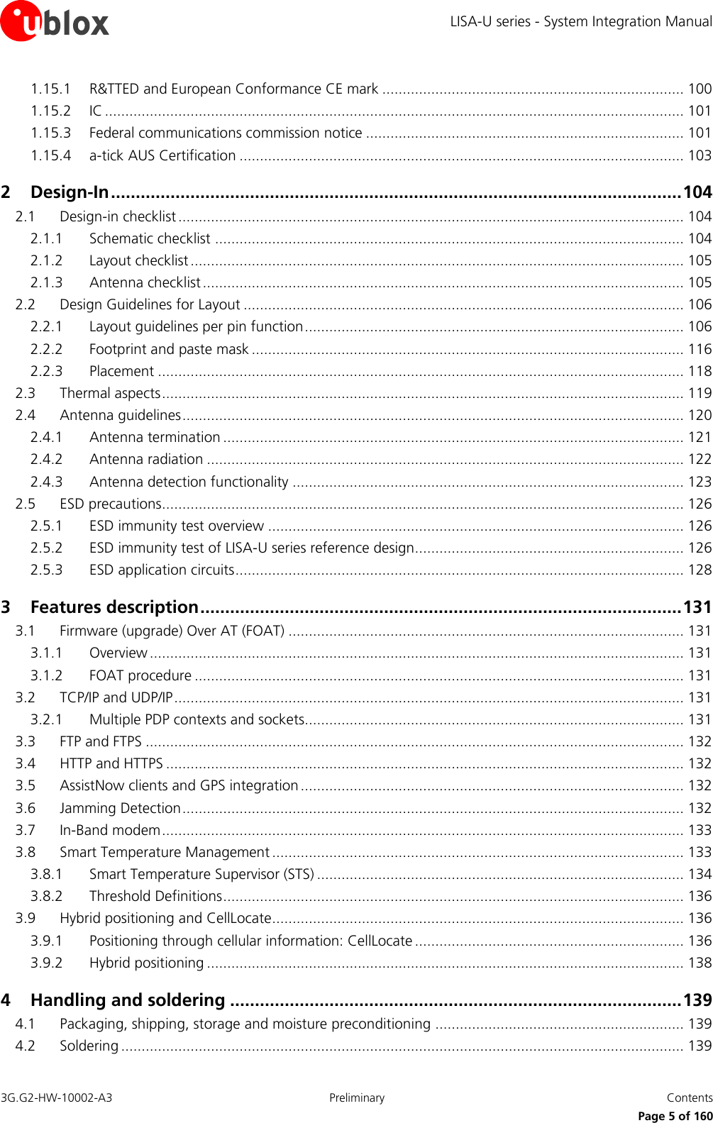
![LISA-U series - System Integration Manual 3G.G2-HW-10002-A3 Preliminary System description Page 17 of 160 1.4 Operating modes LISA-U series modules have several operating modes. Table 5 summarizes the various operating modes and provides general guidelines for operation. Operating Mode Description Features / Remarks Transition condition General Status: Power-down Not-Powered Mode VCC supply not present or below operating range. Microprocessor switched off (not operating). RTC only operates if supplied through V_BCKP pin. Module is switched off. Application interfaces are not accessible. Internal RTC timer operates only if a valid voltage is applied to V_BCKP pin. Module cannot be switched on by a low level on the PWR_ON input, by a rising edge on the RESET_N input, or by a preset RTC alarm. Module can be switched on applying VCC supply. Power-Off Mode VCC supply within operating range. Microprocessor switched off (not operating). Only RTC runs. Module is switched off: normal shutdown by AT+CPWROFF command (refer to u-blox AT Commands Manual [3]), or by PWR_ON held low for more than 1 s (LISA-U2xx-01 only). Application interfaces are not accessible. Only the internal RTC timer in operation. Module can be switched on by a low level on the PWR_ON input, by a rising edge on the RESET_N input, or by a preset RTC alarm. General Status: Normal Operation Idle-Mode Microprocessor runs with 32 kHz as reference oscillator. Module does not accept data signals from an external device. If power saving is enabled, the module automatically enters idle-mode whenever possible. Application interfaces are disabled. If hardware flow control is enabled, the CTS line to ON state indicates that the module is in active mode and the UART interface is enabled: the line is driven in the OFF state when the module is not prepared to accept data by the UART interface. If hardware flow control is disabled, the CTS line is fixed to ON state. Module by default is not set to automatically enter idle-mode whenever possible, unless power saving configuration is enabled by appropriate AT command (refer to u-blox AT Commands Manual [3], AT+UPSV). Module enters automatically idle-mode when power saving is enabled and there is no activity for the defined time interval: Module registered with the network and power saving enabled. Periodically wakes up to active mode to monitor the paging channel for the paging block reception according to network indication Module not registered with the network and power saving is enabled. Periodically wakes up to monitor external activity Module wakes up from idle-mode to active-mode in the following events: Incoming voice or data call RTC alarm occurs Data received on UART interface (refer to 1.9.2) RTS input line set to the ON state by the DTE if the AT+UPSV=2 command is sent to the module (refer to 1.9.2) USB detection, applying 5 V (typ.) to the VUSB_DET pin The connected USB host forces a remote wakeup of the module as USB device (refer to 1.9.3) The connected SPI master indicates to the module that it is ready for transmission or reception, by the SPI/IPC SPI_MRDY input signal (refer to 1.9.4)](https://usermanual.wiki/u-blox/LISAU230/User-Guide-1727756-Page-17.png)
![LISA-U series - System Integration Manual 3G.G2-HW-10002-A3 Preliminary System description Page 18 of 160 Operating Mode Description Features / Remarks Transition condition Active-Mode Microprocessor runs with 26 MHz as reference oscillator. The module is prepared to accept data signals from an external device. Module is switched on and is fully active. The application interfaces are enabled, unless power saving configuration is enabled by the AT+UPSV command (refer to sections 1.9.2.3, 1.9.3.2, 1.9.4.2 and u-blox AT Commands Manual [3]). Power saving is not enabled by default: it can be enabled by the AT+UPSV command (see u-blox AT Commands Manual [3]). If power saving is enabled, the module automatically enters idle-mode and application interfaces are disabled whenever possible (refer to sections 1.9.2.3, 1.9.3.2, 1.9.4.2 and u-blox AT Commands Manual [3], AT+UPSV). Connected-Mode Voice or data call enabled. Microprocessor runs with 26 MHz as reference oscillator. The module is prepared to accept data signals from an external device. The module is switched on and a voice call or a data call (2G/3G) is in progress. Module is fully active. The application interfaces are enabled, unless power saving configuration is enabled by the AT+UPSV command (see section 1.9.2.3, 1.9.3.2, 1.9.4.2 and the u-blox AT Commands Manual [3]). When call terminates, the module returns to the active operating mode. Table 5: Module operating modes summary Transition between the different modes is described in Figure 3. Switch ON:•Apply VCCIf power saving is enabled and there is no activity for a defined time intervalAny wake up event described in the module operating modes summary table aboveIncoming/outgoing call or other dedicated device network communicationCall terminated, communication droppedRemove VCCSwitch ON:•PWR_ON•RESET_N•RTC AlarmNot poweredPower offActiveConnected IdleSwitch OFF:•AT+CPWROFF•PWR_ON (LISA-U2xx-01 only) Figure 3: Operating modes transition](https://usermanual.wiki/u-blox/LISAU230/User-Guide-1727756-Page-18.png)
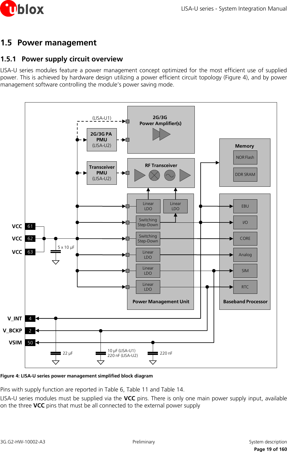
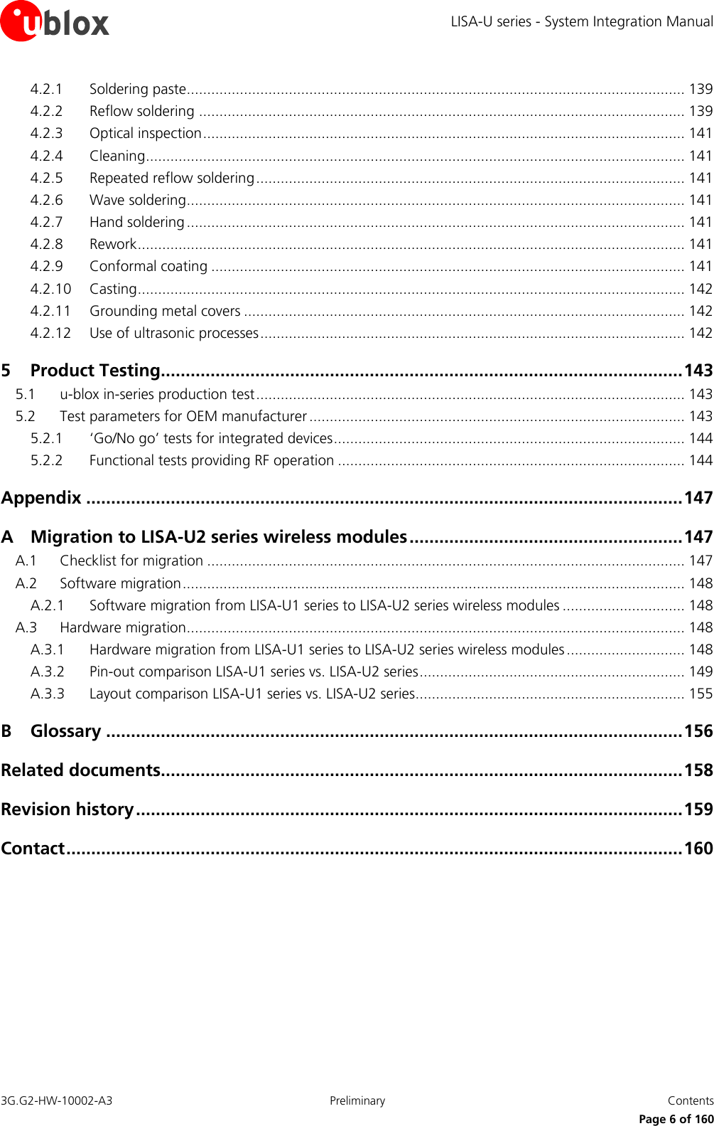
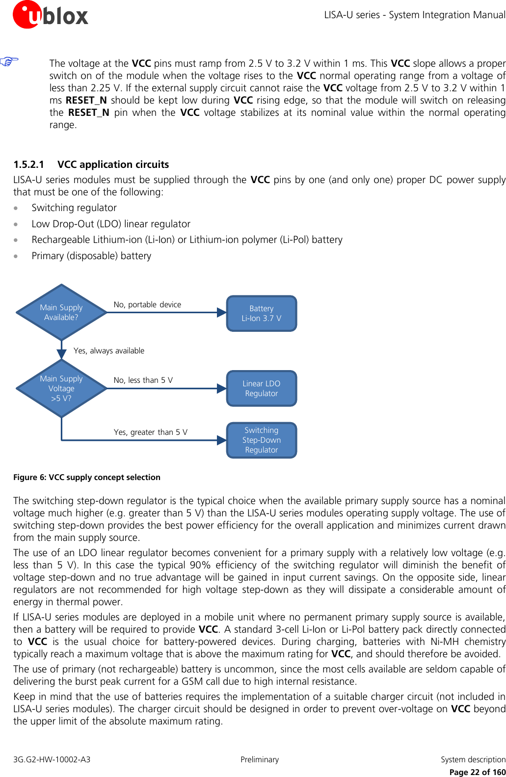
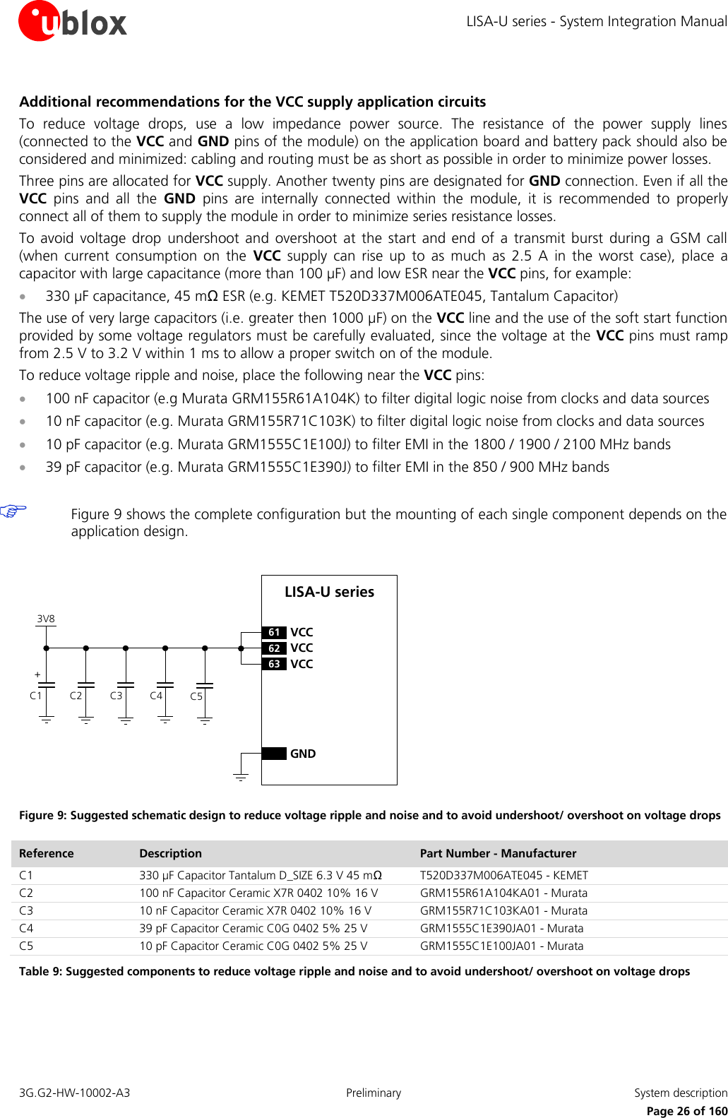
![LISA-U series - System Integration Manual 3G.G2-HW-10002-A3 Preliminary System description Page 20 of 160 The VCC pins are directly connected to the RF power amplifiers and to the integrated Power Management Unit (PMU) within the module: all supply voltages needed by the module are generated from the VCC supply by integrated voltage regulators. V_BCKP is the Real Time Clock (RTC) supply. When the VCC voltage is within the valid operating range, the internal PMU supplies the Real Time Clock and the same supply voltage will be available to the V_BCKP pin. If the VCC voltage is under the minimum operating limit (for example, during not powered mode), the Real Time Clock can be externally supplied via the V_BCKP pin (see section 1.5.4). When a 1.8 V or a 3 V SIM card type is connected, LISA-U series modules automatically supply the SIM card via the VSIM pin. Activation and deactivation of the SIM interface with automatic voltage switch from 1.8 to 3 V is implemented, in accordance to the ISO-IEC 7816-3 specifications. The same voltage domain used internally to supply the digital interfaces is also available on the V_INT pin, to allow more economical and efficient integration of the LISA-U series modules in the final application. The integrated Power Management Unit also provides the control state machine for system start up and system reset control. 1.5.2 Module supply (VCC) The LISA-U series modules must be supplied through the VCC pins by a DC power supply. Voltages must be stable: during operation, the current drawn from VCC can vary by some orders of magnitude, especially due to surging consumption profile of the GSM system (described in the section 1.5.3). It is important that the system power supply circuit is able to support peak power (refer to LISA-U1 series Data Sheet [1] and LISA-U2 series Data Sheet [2] for the detailed specifications). Name Description Remarks VCC Module power supply input VCC pins are internally connected, but all the available pads must be connected to the external supply in order to minimize the power loss due to series resistance. Clean and stable supply is required: low ripple and low voltage drop must be guaranteed. Voltage provided must always be above the minimum limit of the operating range. Consider that during a GSM call there are large current spikes in connected mode. GND Ground GND pins are internally connected but a good (low impedance) external ground can improve RF performance: all available pads must be connected to ground. Table 6: Module supply pins VCC pins ESD sensitivity rating is 1 kV (Human Body Model according to JESD22-A114F). Higher protection level can be required if the line is externally accessible on the application board. Higher protection level can be achieved by mounting an ESD protection (e.g. EPCOS CA05P4S14THSG varistor array) on the line connected to this pin, close to accessible point. The voltage provided to the VCC pins must be within the normal operating range limits as specified in the LISA-U1 series Data Sheet [1] and LISA-U2 series Data Sheet [2]. Complete functionality of the module is only guaranteed within the specified minimum and maximum VCC voltage normal operating range. The module cannot be switched on if the VCC voltage value is below the specified normal operating range minimum limit. Ensure that the input voltage at VCC pins is above the minimum limit of the normal operating range for more than 3 s after the start of the module switch-on sequence.](https://usermanual.wiki/u-blox/LISAU230/User-Guide-1727756-Page-20.png)
![LISA-U series - System Integration Manual 3G.G2-HW-10002-A3 Preliminary System description Page 21 of 160 When LISA-U series modules are in operation, the voltage provided to VCC pins can go outside the normal operating range limits but must be within the extended operating range limits specified in LISA-U1 series Data Sheet [1] and LISA-U2 series Data Sheet [2]. Occasional deviations from the ETSI specifications may occur when the input voltage at VCC pins is outside the normal operating range and is within the extended operating range. LISA-U series modules switch off when VCC voltage value drops below the specified extended operating range minimum limit: ensure that the input voltage at VCC pins never drops below the minimum limit of the extended operating range when the module is switched on, not even during a GSM transmit burst, where the current consumption can rise up to maximum peaks of 2.5 A in case of a mismatched antenna load. Operation above the normal operating range maximum limit is not recommended and extended exposure beyond it may affect device reliability. Stress beyond the VCC absolute maximum ratings can cause permanent damage to the module: if necessary, voltage spikes beyond VCC absolute maximum ratings must be restricted to values within the specified limits by using appropriate protection. When designing the power supply for the application, pay specific attention to power losses and transients. The DC power supply must be able to provide a voltage profile to the VCC pins with the following characteristics: o Voltage drop during transmit slots must be lower than 400 mV o No undershoot or overshoot at the start and at the end of transmit slots o Voltage ripple during transmit slots must be minimized: lower than 70 mVpp if fripple ≤ 200 kHz lower than 10 mVpp if 200 kHz < fripple ≤ 400 kHz lower than 2 mVpp if fripple > 400 kHz TimeundershootovershootripplerippledropVoltage3.8 V (typ)RX slotunused slotunused slotTX slotunused slotunused slotMON slotunused slotRX slotunused slotunused slotTX slotunused slotunused slotMON slotunused slotGSM frame 4.615 ms (1 frame = 8 slots)GSM frame 4.615 ms (1 frame = 8 slots) Figure 5: Description of the VCC voltage profile versus time during a GSM call Any degradation in power supply performance (due to losses, noise or transients) will directly affect the RF performance of the module since the single external DC power source indirectly supplies all the digital and analog interfaces, and also directly supplies the RF power amplifier (PA).](https://usermanual.wiki/u-blox/LISAU230/User-Guide-1727756-Page-21.png)
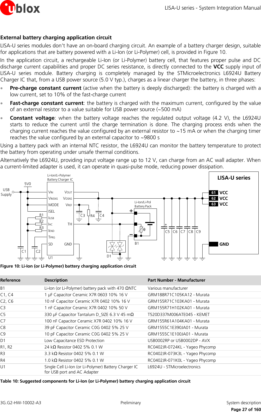
![LISA-U series - System Integration Manual 3G.G2-HW-10002-A3 Preliminary System description Page 28 of 160 1.5.3 Current consumption profiles During operation, the current drawn by the LISA-U series modules through the VCC pins can vary by several orders of magnitude. This ranges from the high peak of current consumption during GSM transmitting bursts at maximum power level in 2G connected mode, to continuous high current drawn in UMTS connected mode, to the low current consumption during power saving in idle-mode. 1.5.3.1 2G connected mode When a GSM call is established, the VCC consumption is determined by the current consumption profile typical of the GSM transmitting and receiving bursts. The current consumption peak during a transmission slot is strictly dependent on the transmitted power, which is regulated by the network. If the module is transmitting in GSM talk mode in the GSM 850 or in the E-GSM 900 band and at the maximum RF power control level (approximately 2 W or 33 dBm in the allocated transmit slot/burst) the current consumption can reach up to 2500 mA (with a highly unmatched antenna) for 576.9 µs (width of the transmit slot/burst) with a periodicity of 4.615 ms (width of 1 frame = 8 slots/burst), so with a 1/8 duty cycle according to GSM TDMA (Time Division Multiple Access). If the module is in GSM connected mode in the DCS 1800 or in the PCS 1900 band, the current consumption figures are lower than the one in the GSM 850 or in the E-GSM 900 band, due to 3GPP transmitter output power specifications (refer to refer to LISA-U1 series Data Sheet [1] and LISA-U2 series Data Sheet [2]). During a GSM call, current consumption is in the order of 60-130 mA in receiving or in monitor bursts and is about 10-40 mA in the inactive unused bursts (low current period). The more relevant contribution to determine the average current consumption is set by the transmitted power in the transmit slot. An example of current consumption profile of the data module in GSM talk mode is shown in Figure 11. Time [ms]RX slotunused slotunused slotTX slotunused slotunused slotMON slotunused slotRX slotunused slotunused slotTX slotunused slotunused slotMON slotunused slotGSM frame 4.615 ms (1 frame = 8 slots)Current [A]200 mA60-130 mA2500 mAPeak current depends on TX powerGSM frame 4.615 ms (1 frame = 8 slots)1.51.00.50.02.52.060-130 mA 10-40 mA Figure 11: VCC current consumption profile versus time during a GSM call (1 TX slot, 1 RX slot), with VCC=3.8 V When a GPRS connection is established there is a different VCC current consumption profile also determined by the transmitting and receiving bursts. In contrast to a GSM call, during a GPRS connection more than one slot can be used to transmit and/or more than one slot can be used to receive. The transmitted power depends on network conditions, which set the peak current consumption, but following the GPRS specifications the maximum transmitted RF power is reduced if more than one slot is used to transmit, so the maximum peak of current consumption is not as high as can be in case of a GSM call. If the module transmits in GPRS class 12 or class 33 connected mode in the GSM 850 or in the E-GSM 900 band at the maximum power control level, the current consumption can reach up to 1600 mA (with unmatched](https://usermanual.wiki/u-blox/LISAU230/User-Guide-1727756-Page-28.png)
![LISA-U series - System Integration Manual 3G.G2-HW-10002-A3 Preliminary System description Page 29 of 160 antenna). This happens for 2.307 ms (width of the 4 transmit slots/bursts) with a periodicity of 4.615 ms (width of 1 frame = 8 slots/bursts), so with a 1/2 duty cycle, according to GSM TDMA. If the module is in GPRS connected mode in the DCS 1800 or in the PCS 1900 band, the current consumption figures are lower than in the GSM 850 or in the E-GSM 900 band, due to 3GPP transmitter output power specifications (refer to LISA-U1 series Data Sheet [1] and LISA-U2 series Data Sheet [2]). Figure 12 reports the current consumption profiles in GPRS class 12 connected mode, in the GSM 850 or in the E-GSM 900 band, with 4 slots used to transmit and 1 slot used to receive. Time [ms]RX slotunused slotTX slotTX slotTX slotTX slotMON slotunused slotRX slotunused slotTX slotTX slotTX slotTX slotMON slotunused slotGSM frame 4.615 ms (1 frame = 8 slots)Current [A]200mA60-130mAPeak current depends on TX powerGSM frame 4.615 ms (1 frame = 8 slots)1.51.00.50.02.52.01600 mA60-130mA10-40mA Figure 12: VCC current consumption profile versus time during a GPRS/EDGE connection (4TX slots, 1 RX slot), with VCC=3.8 V In case of EDGE connections the VCC current consumption profile is very similar to the GPRS current profile, so the image shown in Figure 12, representing the current consumption profile in GPRS class 12 connected mode, is valid for the EDGE class 12 connected mode as well. LISA-U2 series modules support GPRS and EDGE class 33: up to 4 slots can be used to transmit, as in the class 12 mode, and up to 2 slots can be used to receive in the same frame since up to 6 slots can be used in total. So, the VCC current consumption figures in GPRS and EDGE class 33 connected modes are similar to the current profile in GPRS and EDGE class 12 connected modes, since the same number of transmit slots are used. 1.5.3.2 3G connected mode During a 3G connection, the module can transmit and receive continuously due to the Frequency Division Duplex (FDD) mode of operation with the Wideband Code Division Multiple Access (WCDMA). The current consumption depends again on output RF power, which is always regulated by network commands. These power control commands are logically divided into a slot of 666 µs, thus the rate of power change can reach a maximum rate of 1.5 kHz. There are no high current peaks as in the 2G connection, since transmission and reception are continuously enabled due to FDD WCDMA implemented in the 3G that differs from the TDMA implemented in the 2G case. In the worst scenario, corresponding to a continuous transmission and reception at maximum output power (approximately 250 mW or 24 dBm), the current drawn by the module at the VCC pins is in the order of continuous 500-800 mA (refer to LISA-U1 series Data Sheet [1] and LISA-U2 series Data Sheet [2] for detailed values). Even at lowest output RF power (approximately 0.01 µW or -50 dBm), the current still remains in the order of 200 mA due to module baseband processing and transceiver activity. An example of current consumption profile of the data module in UMTS/HSxPA continuous transmission mode is shown in Figure 13.](https://usermanual.wiki/u-blox/LISAU230/User-Guide-1727756-Page-29.png)
![LISA-U series - System Integration Manual 3G.G2-HW-10002-A3 Preliminary System description Page 30 of 160 Time [ms]3G frame 10 ms (1 frame = 15 slots)Current [mA]Depends on TX power170 mA1 slot 666 µs850 mA0300200100500400600700800 Figure 13: VCC current consumption profile versus time during a UMTS/HSPA connection, with VCC=3.8 V When a packet data connection is established, the actual current profile depends on the amount of transmitted packets; there might be some periods of inactivity between allocated slots where current consumption drops about 100 mA. Alternatively, at higher data rates the transmitted power is likely to increase due to the higher quality signal required by the network to cope with enhanced data speed. 1.5.3.3 2G and 3G cyclic idle/active mode (power saving enabled) The power saving configuration is by default disabled, but it can be enabled using the appropriate AT command (refer to u-blox AT Commands Manual [3], AT+UPSV command). When power saving is enabled, the module automatically enters idle-mode whenever possible. When power saving is enabled, the module is registered or attached to a network and a voice or data call is not enabled, the module automatically enters idle-mode whenever possible, but it must periodically monitor the paging channel of the current base station (paging block reception), in accordance to GSM system requirements. When the module monitors the paging channel, it wakes up to active mode, to enable the reception of paging block. In between, the module switches to idle-mode. This is known as GSM discontinuous reception (DRX). The module processor core is activated during the paging block reception, and automatically switches its reference clock frequency from 32 kHz to the 26 MHz used in active-mode. The time period between two paging block receptions is defined by the network (2G or 3G). This is the paging period parameter, fixed by the base station through broadcast channel sent to all users on the same serving cell. In case of 2G network, the time interval between two paging block receptions can be from 470.76 ms (DRX = 2, i.e. width of 2 GSM multiframes = 2 x 51 GSM frames = 2 x 51 x 4.615 ms) up to 2118.42 ms (DRX = 9, i.e. width of 9 GSM multiframes = 9 x 51 frames = 9 x 51 x 4.615 ms). In case of 3G network, the principle is similar but time interval changes from 640 ms (DRX = 6, i.e. the width of 26 x 3G frames = 64 x 10 ms = 640 ms) up to 5120 ms (DRX = 9, i.e. width of 29 x 3G frames = 512 x 10 ms = 5120 ms). An example of a module current consumption profile is shown in Figure 14: the module is registered with the network (2G or 3G), automatically enters idle-mode and periodically wakes up to active mode to monitor the paging channel for paging block reception.](https://usermanual.wiki/u-blox/LISAU230/User-Guide-1727756-Page-30.png)
![LISA-U series - System Integration Manual 3G.G2-HW-10002-A3 Preliminary System description Page 31 of 160 ~30 msIDLE MODE ACTIVE MODE IDLE MODE400-700 µAActive Mode EnabledIdle Mode Enabled400-700 µA2G case: 60-130 mA 3G case: 50-90 mA2G case: 0.44-2.09 s 3G case: 0.61-5.09 sIDLE MODE2G or 3G case: ~30 msACTIVE MODETime [s]Current [mA]150100500Time [ms]Current [mA]1501005005-10 mA 10-25 mA2G case: 60-130 mA 3G case: 50-90 mAPLL EnabledRX Enabled35-40 mADSP Enabled Figure 14: Description of VCC current consumption profile versus time when the module is registered with 2G or 3G networks: the module is in idle-mode and periodically wakes up to active mode to monitor the paging channel for paging block reception 1.5.3.4 2G and 3G fixed active mode (power saving disabled) Power saving configuration is by default disabled, or it can be disabled using the appropriate AT command (refer to u-blox AT Commands Manual [3], AT+UPSV command). When power saving is disabled, the module doesn’t automatically enter idle-mode whenever possible: the module remains in active mode. The module processor core is activated during active-mode, and the 26 MHz reference clock frequency is used. An example of the current consumption profile of the data module when power saving is disabled is shown in Figure 15: the module is registered with the network, active-mode is maintained, and the receiver and the DSP are periodically activated to monitor the paging channel for paging block reception.](https://usermanual.wiki/u-blox/LISAU230/User-Guide-1727756-Page-31.png)
![LISA-U series - System Integration Manual 3G.G2-HW-10002-A3 Preliminary System description Page 32 of 160 ACTIVE MODE10-25 mA10-25 mA2G case: 0.47-2.12 s 3G case: 0.64-5.12 sPaging periodTime [s]Current [mA]150100500Time [ms]Current [mA]15010050010-25 mARX EnabledDSP Enabled35-40 mA2G case: 60-130 mA 3G case: 50-90 mA2G case: 60-130 mA 3G case: 50-90 mA Figure 15: Description of the VCC current consumption profile versus time when power saving is disabled: the active-mode is always held, and the receiver and the DSP are periodically activated to monitor the paging channel for paging block reception 1.5.4 RTC Supply (V_BCKP) The V_BCKP pin connects the supply for the Real Time Clock (RTC) and Power-On / Reset internal logic. This supply domain is internally generated by a linear regulator integrated in the Power Management Unit. The output of this linear regulator is always enabled when the main voltage supply provided to the module through VCC is within the valid operating range, with the module switched-off or powered-on. Name Description Remarks V_BCKP Real Time Clock supply V_BCKP output voltage = 2.3 V (typical) on LISA-U1 series V_BCKP output voltage = 1.8 V (typical) on LISA-U2 series Generated by the module to supply Real Time Clock when VCC supply voltage is within valid operating range. Table 11: Real Time Clock supply pin The V_BCKP pin ESD sensitivity rating is 1 kV (Human Body Model according to JESD22-A114F). Higher protection level could be required if the line is externally accessible on the application board. Higher protection level can be achieved by mounting an ESD protection (e.g. EPCOS CA05P4S14THSG varistor array) on the line connected to this pin, close to accessible point.](https://usermanual.wiki/u-blox/LISAU230/User-Guide-1727756-Page-32.png)
![LISA-U series - System Integration Manual 3G.G2-HW-10002-A3 Preliminary System description Page 33 of 160 The RTC provides the time reference (date and time) of the module, also in power-off mode, when the V_BCKP voltage is within its valid range (specified in the Input characteristics of Supply/Power pins table in LISA-U1 series Data Sheet [1] and LISA-U2 series Data Sheet [2]). The RTC timing is normally used to set the wake-up interval during idle-mode periods between network paging, but is able to provide programmable alarm functions by means of the internal 32.768 kHz clock. The RTC can be supplied from an external back-up battery through the V_BCKP, when the main voltage supply is not provided to the module through VCC. This lets the time reference (date and time) run until the V_BCKP voltage is within its valid range, even when the main supply is not provided to the module. The RTC oscillator doesn't necessarily stop operation (i.e. the RTC counting doesn't necessarily stop) when V_BCKP voltage value drops below the specified operating range minimum limit (1.00 V): the RTC value read after a system restart could be not reliable as explained in the following Table 12. V_BCKP voltage value RTC value reliability Notes 1.00 V < V_BCKP < 1.90 V (LISA-U2 series) 1.00 V < V_BCKP < 2.50 V (LISA-U1 series) RTC oscillator doesn't stop operation RTC value read after a restart of the system is reliable V_BCKP within operating range 0.05 V < V_BCKP < 1.00 V RTC oscillator doesn't necessarily stop operation RTC value read after a restart of the system is not reliable V_BCKP below operating range 0.00 V < V_BCKP < 0.05 V RTC oscillator stops operation RTC value read after a restart of the system is reliable V_BCKP below operating range Table 12: RTC value reliability as function of V_BCKP voltage value Consider that the module cannot switch on if a valid voltage is not present on VCC even when the RTC is supplied through V_BCKP (meaning that VCC is mandatory to switch-on the module). The RTC has very low power consumption, but is highly temperature dependent. For example at 25°C, with the V_BCKP voltage equal to the typical output value, the power consumption is approximately 2 µA (refer to the Input characteristics of Supply/Power pins table in the LISA-U1 series Data Sheet [1] and in the LISA-U2 series Data Sheet [2] for the detailed specification), whereas at 70°C and an equal voltage the power consumption increases to 5-10 µA. The internal regulator for V_BCKP is optimized for low leakage current and very light loads. It is not recommended to use V_BCKP to supply external loads. If V_BCKP is left unconnected and the module main voltage supply is removed from VCC, the RTC is supplied from the bypass capacitor mounted inside the module. However, this capacitor is not able to provide a long buffering time: within few milliseconds the voltage on V_BCKP will go below the valid range (1 V min). This has no impact on wireless connectivity, as all the functionalities of the module do not rely on date and time setting. Leave V_BCKP unconnected if the RTC is not required when the VCC supply is removed. The date and time will not be updated when VCC is disconnected. If VCC is always supplied, then the internal regulator is supplied from the main supply and there is no need for an external component on V_BCKP. If RTC is required to run for a time interval of T [s] at 25°C when VCC supply is removed, place a capacitor with a nominal capacitance of C [µF] at the V_BCKP pin. Choose the capacitor using the following formula: C [µF] = (Current_Consumption [µA] x T [s]) / Voltage_Drop [V] = 1.92 x T [s] for LISA-U1 series = 2.50 x T [s] for LISA-U2 series For example, a 100 µF capacitor (such as the Murata GRM43SR60J107M) can be placed at V_BCKP to provide a long buffering time. This capacitor will hold V_BCKP voltage within its valid range for around 50 s at 25°C, after the VCC supply is removed. If a very long buffering time is required, a 70 mF super-capacitor (e.g. Seiko](https://usermanual.wiki/u-blox/LISAU230/User-Guide-1727756-Page-33.png)
![LISA-U series - System Integration Manual 3G.G2-HW-10002-A3 Preliminary System description Page 34 of 160 Instruments XH414H-IV01E) can be placed at V_BCKP, with a 4.7 k series resistor to hold the V_BCKP voltage within its valid range for approximately 10 hours at 25°C, after the VCC supply is removed. The purpose of the series resistor is to limit the capacitor charging current due to the large capacitor specifications, and also to let a fast rise time of the voltage value at the V_BCKP pin after VCC supply has been provided. These capacitors will allow the time reference to run during battery disconnection. LISA-U seriesC1(a)2V_BCKPR2LISA-U seriesC2(superCap)(b)2V_BCKPD3LISA-U seriesB3(c)2V_BCKP Figure 16: Real time clock supply (V_BCKP) application circuits: (a) using a 100 µF capacitor to let the RTC run for ~50 s after VCC removal; (b) using a 70 mF capacitor to let RTC run for ~10 hours after VCC removal; (c) using a non-rechargeable battery Reference Description Part Number - Manufacturer C1 100 µF Tantalum Capacitor GRM43SR60J107M - Murata R2 4.7 kΩ Resistor 0402 5% 0.1 W RC0402JR-074K7L - Yageo Phycomp C2 70 mF Capacitor XH414H-IV01E - Seiko Instruments Table 13: Example of components for V_BCKP buffering If longer buffering time is required to allow the time reference to run during a disconnection of the VCC supply, then an external battery can be connected to V_BCKP pin. The battery should be able to provide a proper nominal voltage and must never exceed the maximum operating voltage for V_BCKP (specified in the Input characteristics of Supply/Power pins table in LISA-U1 series Data Sheet [1] and in LISA-U2 series Data Sheet [2]). The connection of the battery to V_BCKP should be done with a suitable series resistor for a rechargeable battery, or with an appropriate series diode for a non-rechargeable battery. The purpose of the series resistor is to limit the battery charging current due to the battery specifications, and also to allow a fast rise time of the voltage value at the V_BCKP pin after the VCC supply has been provided. The purpose of the series diode is to avoid a current flow from the module V_BCKP pin to the non-rechargeable battery. Combining a LISA-U series wireless module with a u-blox GPS receiver, the VCC supply of the GPS receiver is controlled by the wireless module by means of the GPS supply enable function provided by the GPIO2 of the wireless module. In this case the V_BCKP supply output of the LISA-U series wireless module can be connected to the V_BCKP backup supply input pin of the GPS receiver to provide the supply for the GPS real time clock and backup RAM when the VCC supply of the wireless module is within its operating range and the VCC supply of the GPS receiver is disabled. This enables the u-blox GPS receiver to recover from a power breakdown with either a Hotstart or a Warmstart (depending on the duration of the GPS VCC outage) and to maintain the configuration settings saved in the backup RAM. Refer to section 1.10 for more details regarding the application circuit with a u-blox GPS receiver. 1.5.5 Interface supply (V_INT) The same voltage domain used internally to supply the digital interfaces is also available on the V_INT pin. The internal regulator that generates the V_INT supply is a switching step down converter that is directly supplied from VCC. The voltage regulator output is set to 1.8 V (typical) when the module is switched on and is disabled when the module is switched off or when the RESET_N pin is forced the low level. The switching regulator operates in Pulse Width Modulation (PWM) for high output current mode but automatically switches to Pulse](https://usermanual.wiki/u-blox/LISAU230/User-Guide-1727756-Page-34.png)
![LISA-U series - System Integration Manual 3G.G2-HW-10002-A3 Preliminary System description Page 35 of 160 Frequency Modulation (PFM) at low output loads for greater efficiency, e.g. when the module is in idle-mode between paging periods. Name Description Remarks V_INT Digital Interfaces supply output V_INT = 1.8V (typical) generated by the module when it is switched-on and the RESET_N (external reset input pin) is not forced to the low level. V_INT is the internal supply for digital interfaces. The user may draw limited current from this supply rail. Table 14: Interface supply pin The V_INT pin ESD sensitivity rating is 1 kV (Human Body Model according to JESD22-A114F). Higher protection level could be required if the line is externally accessible on the application board. Higher protection level can be achieved by mounting an ESD protection (e.g. EPCOS CA05P4S14THSG varistor array) on the line connected to this pin, close to accessible point. Since it supplies internal digital circuits (see Figure 4), V_INT is not suited to directly supply any sensitive analog circuit: the voltage ripple can range from 15 mVpp during active mode (PWM), to 70 mVpp in idle-mode (PFM). V_INT can be used to supply external digital circuits operating at the same voltage level as the digital interface pins, i.e. 1.8 V (typical). It is not recommended to supply analog circuitry without adequate filtering for digital noise. Don’t apply loads which might exceed the limit for maximum available current from V_INT supply, as this can cause malfunctions in internal circuitry supplies to the same domain. The detailed electrical characteristics are described in LISA-U1 series Data Sheet [1] and LISA-U2 series Data Sheet [2]. V_INT can only be used as an output; don’t connect any external regulator on V_INT. If not used, this pin should be left unconnected. The V_INT digital interfaces supply output is mainly used to: Pull-up DDC (I2C) interface signals (see section 1.10.2 for more details) Pull-up SIM detection signal (see section 1.8 for more details) Supply voltage translators to connect digital interfaces of the module to a 3.0 V device (see section 1.9.2.4) Indicate when the module is switched on and the RESET_N (external reset input) is not forced low 1.6 System functions 1.6.1 Module power-on The power-on sequence of LISA-U series modules is initiated in one of these ways: Rising edge on the VCC pin to a valid voltage as module supply (i.e. applying module supply) Low level on the PWR_ON pin (i.e. forcing to the low level the pin normally high by external pull-up) Rising edge on the RESET_N pin (i.e. releasing from low level the pin, normally high by internal pull-up) RTC alarm (i.e. pre-programmed scheduled time by AT+CALA command)](https://usermanual.wiki/u-blox/LISAU230/User-Guide-1727756-Page-35.png)
![LISA-U series - System Integration Manual 3G.G2-HW-10002-A3 Preliminary System description Page 36 of 160 Name Description Remarks PWR_ON Power-on input PWR_ON pin has high input impedance. Do not keep floating in noisy environment: external pull-up required. Table 15: Power-on pin The PWR_ON pin ESD sensitivity rating is 1 kV (Human Body Model according to JESD22-A114F). Higher protection level could be required if the line is externally accessible on the application board. Higher protection level can be achieved by mounting an ESD protection (e.g. EPCOS CA05P4S14THSG varistor array) on the line connected to this pin, close to accessible point. 1.6.1.1 Rising edge on VCC When a supply is connected to VCC pins, the module supply supervision circuit controls the subsequent activation of the power up state machines: the module is switched on when the voltage rises up to the VCC normal operating range minimum limit starting from a voltage value lower than 2.25 V (refer to LISA-U1 series Data Sheet [1] and LISA-U2 series Data Sheet [2] for the VCC normal operating range minimum limit). The voltage at the VCC pins must ramp from 2.5 V to 3.2 V within 1 ms to switch on the module. 1.6.1.2 Low level on PWR_ON The module power-on sequence starts when a low level is forced on the PWR_ON input for at least 5 ms. The electrical characteristics of the PWR_ON input pin are slightly different between LISA-U1 series and LISA-U2 series modules, and are different from the other digital I/O interfaces: the pin provides different input voltage thresholds and is tolerant of voltages up to the module supply level. The detailed electrical characteristics are described in LISA-U1 series Data Sheet [1] and LISA-U2 series Data Sheet [2]. The PWR_ON pin has high input impedance and is weakly pulled to the high level on the module. Avoid keeping it floating in a noisy environment. To hold the high logic level stable, the PWR_ON pin must be connected to a pull-up resistor (e.g. 100 kΩ) biased by the V_BCKP supply pin of the module. Following are some typical examples of application circuits to turn the module on using the PWR_ON input pin. The simplest way to turn on the module is to use a push button that shorts the PWR_ON input to ground: in this case the V_BCKP supply pin can be used to bias the pull-up resistor. If PWR_ON input is connected to an external device (e.g. application processor), it is suggested to use an open drain output on the external device with an external pull-up resistor (e.g. 100 kΩ) biased by the V_BCKP supply pin of the module. A push-pull output of an application processor can also be used: in this case the pull-up can be used to pull the PWR_ON level high when the application processor is switched off. If the high-level voltage of the push-pull output pin of the application processor is greater than the maximum input voltage operating range of the V_BCKP pin (refer to the V_BCKP Input characteristics of Supply/Power pins table in LISA-U1 series Data Sheet [1] and LISA-U2 series Data Sheet [2]), the V_BCKP supply cannot be used to bias the pull-up resistor: the supply rail of the application processor or the VCC supply could be used, but this will increase the V_BCKP (RTC supply) current consumption when the module is in not-powered mode (VCC supply not present). Using a push-pull output of the external device, take care to fix the proper level in all the possible scenarios to avoid an inappropriate switch-on of the module.](https://usermanual.wiki/u-blox/LISAU230/User-Guide-1727756-Page-36.png)
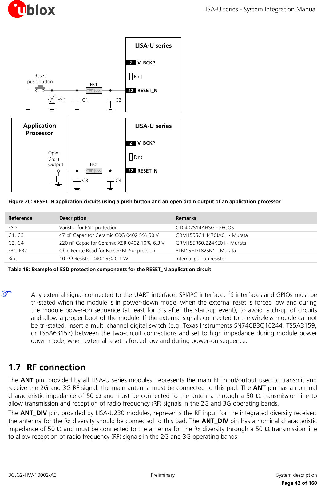
![LISA-U series - System Integration Manual 3G.G2-HW-10002-A3 Preliminary System description Page 37 of 160 LISA-U seriesRext2V_BCKP19 PWR_ONPower-on push buttonESDOpen Drain OutputApplication ProcessorLISA-U seriesRext2V_BCKP19 PWR_ON Figure 17: PWR_ON application circuits using a push button and an open drain output of an application processor Reference Description Remarks Rext 100 kΩ Resistor 0402 5% 0.1 W External pull-up resistor ESD CT0402S14AHSG - EPCOS Varistor array for ESD protection Table 16: Example of pull-up resistor and ESD protection for the PWR_ON application circuits 1.6.1.3 Rising edge on RESET_N LISA-U series modules can be switched on by means of the RESET_N input pin: the RESET_N signal must be forced low for at least 50 ms and then released to generate a rising edge that starts the module power-on sequence. RESET_N input pin can also be used to perform an “external” or “hardware” reset of the module, as described in the section 1.6.3. Electrical characteristics of the LISA-U series RESET_N input are slightly different from the other digital I/O interfaces: the pin provides different input voltage thresholds. Detailed electrical characteristics are described in LISA-U1 series Data Sheet [1] and LISA-U2 series Data Sheet [2]. RESET_N is pulled high to V_BCKP by an integrated pull-up resistor also when the module is in power-off mode. Therefore an external pull-up is not required on the application board. The simplest way to switch on the module by means of the RESET_N input pin is to use a push button that shorts the RESET_N pin to ground: the module will be switched on at the release of the push button, since the RESET_N will be forced to the high level by the integrated pull-up resistor, generating a rising edge. If RESET_N is connected to an external device (e.g. an application processor on an application board) an open drain output can be directly connected without any external pull-up. A push-pull output can be used too: in this case make sure that the high level voltage of the push-pull circuit is below the maximum voltage operating range of the RESET_N pin (specified in the RESET_N pin characteristics table in LISA-U1 series Data Sheet [1] and LISA-U2 series Data Sheet [2]). To avoid unwanted power-on or reset of the module make sure to fix the proper level at the RESET_N input pin in all possible scenarios. Some typical examples of application circuits using the RESET_N input pin are described in the section 1.6.3.](https://usermanual.wiki/u-blox/LISAU230/User-Guide-1727756-Page-37.png)
![LISA-U series - System Integration Manual 3G.G2-HW-10002-A3 Preliminary System description Page 38 of 160 1.6.1.4 Real Time Clock (RTC) alarm If a voltage within the operating range is maintained at the VCC pin, the module can be switched on by the RTC alarm when the RTC system reaches a pre-programmed scheduled time (refer to the u-blox AT Commands Manual [3], AT+CALA command). The RTC system will then initiate the boot sequence by instructing the Power Management Unit to turn on power. Also included in this setup is an interrupt signal from the RTC block to indicate to the baseband processor that an RTC event has occurred. 1.6.1.5 Additional considerations The module is switched on when the VCC voltage rises up to the normal operating range (i.e. applying module supply): the first time that the module is used, it is switched on in this way. Then, LISA-U series modules can be switched off by means of the AT+CPWROFF command. When the module is in power-off mode, i.e. the AT+CPWROFF command has been sent and a voltage value within the normal operating range limits is still provided to the VCC pin, the digital input-output pads of the baseband chipset (i.e. all the digital pins of the module) are locked in tri-state (i.e. floating). The power down tri-state function isolates the module pins from its environment, when no proper operation of the outputs can be guaranteed. The module can be switched on from power-off mode by forcing a proper start-up event (i.e. PWR_ON low, RESET_N release or RTC alarm). After the detection of a start-up event, all the digital pins of the module are held in tri-state until all the internal LDO voltage regulators are turned on in a defined power-on sequence. Then, as described in Figure 18, the baseband core is still held in reset state for a time interval: the internal reset signal (which is not available on a module pin) is still low and any signal from the module digital interfaces is held in reset state. The reset state of all the digital pins is reported in the pin description table of LISA-U1 series Data Sheet [1] and LISA-U2 series Data Sheet [2]. When the internal signal is released, the configuration of the module interfaces starts: during this phase any digital pin is set in a proper sequence from the reset state to the default operational configuration. Finally, the module is fully ready to operate when all interfaces are configured. VCCV_BCKPPWR_ONV_INTInternal ResetSystem StateBB Pads StateInternal Reset → Operational OperationalTristate / Floating Internal ResetOFFONStart-up event0 ms~5 ms~6 ms~35 ms~3 sPWR_ON can be set highStart of interface configurationAll interfaces are configured Figure 18: LISA-U series power-on sequence description The Internal Reset signal is not available on a module pin. Any external signal connected to the UART interface, SPI/IPC interface, I2S interfaces and GPIOs must be tri-stated when the module is in power-down mode, when the external reset is forced low and during the module power-on sequence (at least for 3 s after the start-up event), to avoid latch-up of circuits](https://usermanual.wiki/u-blox/LISAU230/User-Guide-1727756-Page-38.png)
![LISA-U series - System Integration Manual 3G.G2-HW-10002-A3 Preliminary System description Page 39 of 160 and let a proper boot of the module. If the external signals connected to the wireless module cannot be tri-stated, insert a multi channel digital switch (e.g. Texas Instruments SN74CB3Q16244, TS5A3159, or TS5A63157) between the two-circuit connections and set to high impedance during module power down mode, when external reset is forced low and during power on sequence. 1.6.2 Module power-off The correct way to switch off LISA-U series modules is by means of +CPWROFF AT command (more details in u-blox AT Commands Manual [3]): in this way the current parameter settings are saved in the module’s non-volatile memory and a proper network detach is performed. LISA-U2xx-01 modules can also be properly switched off by means of the PWR_ON input pin: the PWR_ON signal must be held to the low logic level for more than 1 s to start the module power-off sequence. In this way, current parameter settings are saved in LISA-U2xx-01 module’s non-volatile memory and a correct network detach is performed: the same sequence is performed as by the +CPWROFF AT command. An under-voltage shutdown occurs on LISA-U series modules when the VCC supply is removed, but in this case the current parameter settings are not saved in the module’s non-volatile memory and a proper network detach cannot be performed. The power-off sequence by means of +CPWROFF AT command is described in Figure 19. When the +CPWROFF AT command is sent, the module starts the switch-off routine replying OK on the AT interface. At the end of the switch-off routine, all digital pins are locked in tri-state by the module and all the internal LDO voltage regulators except the RTC supply (V_BCKP) are turned off in a defined power-off sequence. The module remains in power-off mode as long as a switch on event doesn’t occur (i.e. applying a low level on the PWR_ON pin, or releasing from low level the RESET_N pin, or by a pre-programmed RTC alarm), and enters not-powered mode if the supply is removed from the VCC pin. Current parameter settings are stored to the module’s non-volatile memory and a network detach is performed before the OK reply from AT+CPWROFF command on all LISA-U series modules except LISA-U1xx-00 versions. Storage of parameters and network detach are performed before the end of the switch-off routine, but not necessary before the OK reply from AT+CPWROFF command on LISA-U1xx-00 versions. Since the time to perform a network detach depends on the network settings, the duration of the switch off routine phases can differ from the typical values reported in Figure 19.](https://usermanual.wiki/u-blox/LISAU230/User-Guide-1727756-Page-39.png)
![LISA-U series - System Integration Manual 3G.G2-HW-10002-A3 Preliminary System description Page 40 of 160 VCCV_BCKPPWR_ONV_INTInternal ResetSystem StateBB Pads State OperationalOFFTristate / Floating ONOperational → Tristate / FloatingAT+CPWROFFsent to the module0 ms~50 ms~400 msOKreplied by the module Figure 19: LISA-U series Power-off sequence description The Internal Reset signal is not available on a module pin. Tristated pins are always subject to floating caused by noise: to prevent unwanted effects, fix them with proper pull-up or pull down resistors to stable voltage rails to fix their level when the module is in Power down state. Any external signal connected to the UART interface, SPI/IPC interface, I2S interfaces and GPIOs must be tri-stated when the module is in power-down mode, when the external reset is forced low and during the module power-on sequence (at least for 3 s after the start-up event), to avoid latch-up of circuits and allow a proper boot of the module. If the external signals connected to the wireless module cannot be tri-stated, insert a multi channel digital switch (e.g. Texas Instruments SN74CB3Q16244, TS5A3159, or TS5A63157) between the two-circuit connections and set to high impedance during module power down mode, when external reset is forced low and during power-on sequence. 1.6.3 Module reset LISA-U series modules reset can be performed in one of 2 ways: Forcing a low level on the RESET_N input pin, causing an “external” or “hardware” reset Via AT command, causing an “internal” or “software” reset RESET_N input pin: force low for at least 50 ms; either an “external” or “hardware” reset is performed. This causes an asynchronous reset of the entire module, including the integrated Power Management Unit, except for the RTC internal block: the V_INT interfaces supply is switched off and all the digital pins are tri-stated, but the V_BCKP supply and the RTC block are enabled. Forcing an “external” or “hardware” reset, the current parameter settings are not saved in the module’s non-volatile memory and a proper network detach is not performed. AT+CFUN command (more details in u-blox AT Commands Manual [3]): in this case an “internal” or “software” reset is performed, causing an asynchronous reset of the baseband processor, excluding the integrated Power Management Unit and the RTC internal block: the V_INT interfaces supply is enabled and each digital pin is set in its internal reset state (reported in the pin description table in LISA-U1 series Data Sheet [1] and LISA-U2 series Data Sheet [2]), the V_BCKP supply and the RTC block are enabled. Forcing an “internal” or](https://usermanual.wiki/u-blox/LISAU230/User-Guide-1727756-Page-40.png)
![LISA-U series - System Integration Manual 3G.G2-HW-10002-A3 Preliminary System description Page 41 of 160 “software” reset, the current parameter settings are saved in the module’s non-volatile memory and a proper network detach is performed. When RESET_N is released from the low level, the module automatically starts its power-on sequence from the reset state. The same procedure is followed for the module reset via AT command after having performed the network detach and the parameter saving in non-volatile memory. The internal reset state of all digital pins is reported in the pin description table in LISA-U1 series Data Sheet [1] and LISA-U2 series Data Sheet [2]. Name Description Remarks RESET_N External reset input Internal 10 k pull-up to V_BCKP Table 17: Reset pin The RESET_N pin ESD sensitivity rating is 1 kV (Human Body Model according to JESD22-A114F). Higher protection level could be required if the line is externally accessible on the application board. Higher protection level can be achieved by mounting an ESD protection (e.g. EPCOS CA05P4S14THSG varistor array) on the line connected to this pin, close to accessible point. For more details about RESET_N circuit precautions for ESD immunity please refer to chapter 2.5.3. The electrical characteristics of RESET_N are different from the other digital I/O interfaces. The detailed electrical characteristics are described in LISA-U1 series Data Sheet [1] and LISA-U2 series Data Sheet [2]. RESET_N is pulled high by an integrated 10 k pull-up resistor to V_BCKP. Therefore an external pull-up is not required on the application board. Following are some typical examples of application circuits using the RESET_N input pin. The simplest way to reset the module is to use a push button that shorts the RESET_N pin to ground. If RESET_N is connected to an external device (e.g. an application processor on an application board) an open drain output can be directly connected without any external pull-up. A push-pull output can be used too: in this case make sure that the high level voltage of the push-pull circuit is below the maximum voltage operating range of the RESET_N pin (specified in the RESET_N pin characteristics table in LISA-U1 series Data Sheet [1] and LISA-U2 series Data Sheet [2]). To avoid unwanted reset of the module make sure to fix the proper level at the RESET_N input pin in all possible scenarios. As ESD immunity test precaution, a 47 pF bypass capacitor (e.g. Murata GRM1555C1H470JA01) and a series ferrite bead (e.g. Murata BLM15HD182SN1) must be added on the RESET_N line pin of LISA-U1 series modules and an additional 220 nF bypass capacitor (e.g. Murata GRM155R60J224KE01) must be added as close as possible to the RESET_N pin of LISA-U2 series modules to avoid a module reset caused by an electrostatic discharge applied to the application board (for more details, refer to chapter 2.5.3).](https://usermanual.wiki/u-blox/LISAU230/User-Guide-1727756-Page-41.png)
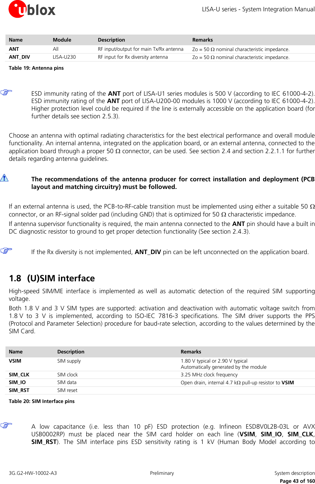
![LISA-U series - System Integration Manual 3G.G2-HW-10002-A3 Preliminary System description Page 46 of 160 1.9 Serial communication LISA-U series modules provide the following serial communication interfaces where AT command interface and Packet-Switched / Circuit-Switched Data communication are concurrently available: One asynchronous serial interface (UART) that provides complete RS-232 functionality conforming to ITU-T V.24 Recommendation [4], with limited data rate. The UART interface can be used for firmware upgrade One Inter Processor Communication (IPC) interface that includes a synchronous SPI-compatible interface, with maximum data rate of 26 Mb/s One high-speed USB 2.0 compliant interface, with maximum data rate of 480 Mb/s. The single USB interface implements several logical devices. Each device is a USB communications device class (or USB CDC), that is a composite Universal Serial Bus device class. The USB interface can be used for firmware upgrade The LISA-U series modules are designed to operate as an HSPA wireless modem, which represents the data circuit-terminating equipment (DCE) as described by the ITU-T V.24 Recommendation [4]. A customer application processor connected to the module through one of the interfaces represents the data terminal equipment (DTE). All the interfaces listed above are controlled and operated with: AT commands according to 3GPP TS 27.007 [5] AT commands according to 3GPP TS 27.005 [6] AT commands according to 3GPP TS 27.010 [7] u-blox AT commands For the complete list of supported AT commands and their syntax refer to the u-blox AT Commands Manual [3]. The following serial communication interfaces can be used for firmware upgrade: The UART interface, using the RxD and TxD lines only The USB interface, using all the lines provided (VUSB_DET, USB_D+ and USB_D-) To directly enable PC (or similar) connection to the module for firmware upgrade, provide direct access on the application board to the VUSB_DET, USB_D+ and USB_D- lines of the module (or to the RxD and TxD lines). Also provide access to the PWR_ON or the RESET_N pins, or enable the DC supply connected to the VCC pin to start the module firmware upgrade (see Firmware Update Application Note [17]). The following sub-chapters describe the serial interfaces configuration and provide a detailed description of each interface for the application circuits. 1.9.1 Serial interfaces configuration UART, USB and SPI/IPC serial interfaces are available as AT command interface and for Packet-Switched / Circuit-Switched Data communication. The serial interfaces are configured as described in Table 22 (for information about further settings, please refer to the u-blox AT Commands Manual [3]).](https://usermanual.wiki/u-blox/LISAU230/User-Guide-1727756-Page-46.png)
![LISA-U series - System Integration Manual 3G.G2-HW-10002-A3 Preliminary System description Page 47 of 160 Interface AT Settings Comments UART interface Enabled Multiplexing mode can be enabled by AT+CMUX command providing following channels: Channel 0: control channel Channel 1 – 5: AT commands /data connection Channel 6: GPS tunneling All LISA-U2 series modules versions except LISA-U200-00 provide an additional channel: Channel 7: SIM Access Profile dedicated port AT+IPR=115200 Baud rate: 115200 b/s AT+ICF=3,1 Frame format: 8 bits, no parity, 1 stop bit AT&K3 HW flow control enabled AT&S1 DSR line set ON in data mode and set OFF in command mode AT&D1 Upon an ON-to-OFF transition of DTR, the DCE enters online command state and issues an OK result code AT&C1 Circuit 109 changes in accordance with the Carrier detect status; ON if the Carrier is detected, OFF otherwise USB interface Enabled 6 CDCs are available, configured as described in the following list: USB1: AT commands / data connection USB2: AT commands / data connection USB3: AT commands / data connection USB4: GPS tunneling dedicated port USB5: 2G and BB trace dedicated port USB6: 3G trace dedicated port All LISA-U2 series modules versions except LISA-U200-00 provide an additional CDC: USB7: SIM Access Profile dedicated port AT&K3 HW flow control enabled AT&S1 DSR line set ON in data mode and set OFF in command mode AT&D1 Upon an ON-to-OFF transition of DTR, the DCE enters online command state and issues an OK result code AT&C1 Circuit 109 changes in accordance with the Carrier detect status; ON if the Carrier is detected, OFF otherwise SPI interface Enabled Multiplexing mode can be enabled by AT+CMUX command providing following channels: Channel 0: control channel Channel 1 – 5: AT commands /data connection Channel 6: GPS tunneling All LISA-U2 series modules versions except LISA-U200-00 provide an additional channel: Channel 7: SIM Access Profile dedicated port AT&K3 HW flow control enabled AT&S1 DSR line set ON in data mode and set OFF in command mode AT&D1 Upon an ON-to-OFF transition of DTR, the DCE enters online command state and issues an OK result code AT&C1 Circuit 109 changes in accordance with the Carrier detect status; ON if the Carrier is detected, OFF otherwise Table 22: Default serial interfaces configuration 1.9.2 Asynchronous serial interface (UART) The UART interface is a 9-wire unbalanced asynchronous serial interface that provides AT commands interface, PSD and CSD data communication, firmware upgrade. UART interface provides RS-232 functionality conforming to the ITU-T V.24 Recommendation (more details available in ITU Recommendation [4]), with CMOS compatible signal levels: 0 V for low data bit or ON state, and 1.8 V for high data bit or OFF state. Two different external voltage translators (e.g. Maxim MAX3237E and Texas Instruments SN74AVC8T245PW) could be used to provide full RS-232 (9 lines) compatible signal levels. The Texas Instruments chip provides the translation from 1.8 V to 3.3 V, while the Maxim chip provides the necessary RS-232 compatible signal towards the external connector. If a UART interface with only 5 lines is needed, the Maxim 13234E voltage level translator can be used. This chip translates the voltage levels from 1.8 V (module](https://usermanual.wiki/u-blox/LISAU230/User-Guide-1727756-Page-47.png)
![LISA-U series - System Integration Manual 3G.G2-HW-10002-A3 Preliminary System description Page 48 of 160 side) to the RS-232 standard. For detailed electrical characteristics refer to LISA-U1 series Data Sheet [1] and LISA-U2 series Data Sheet [2]. The LISA-U series modules are designed to operate as an HSPA wireless modem, which represents the data circuit-terminating equipment (DCE) as described by the ITU-T V.24 Recommendation [4]. A customer application processor connected to the module through the UART interface represents the data terminal equipment (DTE). The signal names of the LISA-U series modules UART interface conform to the ITU-T V.24 Recommendation [4]. UART interfaces include the following lines: Name Description Remarks DSR Data set ready Module output Circuit 107 (Data set ready) in ITU-T V.24 RI Ring Indicator Module output Circuit 125 (Calling indicator) in ITU-T V.24 DCD Data carrier detect Module output Circuit 109 (Data channel received line signal detector) in ITU-T V.24 DTR Data terminal ready Module input Circuit 108/2 (Data terminal ready) in ITU-T V.24 Internal active pull-up to V_INT (1.8 V) enabled. RTS Ready to send Module hardware flow control input Circuit 105 (Request to send) in ITU-T V.24 Internal active pull-up to V_INT (1.8 V) enabled. CTS Clear to send Module hardware flow control output Circuit 106 (Ready for sending) in ITU-T V.24 TxD Transmitted data Module data input Circuit 103 (Transmitted data) in ITU-T V.24 Internal active pull-up to V_INT (1.8 V) enabled. RxD Received data Module data output Circuit 104 (Received data) in ITU-T V.24 GND Ground Table 23: UART interface signals The UART interface pins ESD sensitivity rating is 1 kV (Human Body Model according to JESD22-A114F). Higher protection level could be required if the lines are externally accessible on the application board. Higher protection level can be achieved by mounting an ESD protection (e.g. EPCOS CA05P4S14THSG varistor array) on the lines connected to these pins, close to accessible points. 1.9.2.1 UART features All flow control handshakes are supported by the UART interface and can be set by appropriate AT commands (see u-blox AT Commands Manual [3], &K, +IFC, \Q AT commands): hardware flow control (RTS/CTS), software flow control (XON/XOFF), or none flow control. Hardware flow control is enabled by default. The following baud rates can be configured using AT commands: 1200 b/s 2400 b/s](https://usermanual.wiki/u-blox/LISAU230/User-Guide-1727756-Page-48.png)
![LISA-U series - System Integration Manual 3G.G2-HW-10002-A3 Preliminary System description Page 49 of 160 4800 b/s 9600 b/s 19200 b/s 38400 b/s 57600 b/s 115200 b/s 230400 b/s 460800 b/s The default baud rate is 115200 b/s. Autobauding is not supported. The frame format can be: 8N1 (8 data bits, No parity, 1 stop bit) 8E1 (8 data bits, even parity, 1 stop bit) 8O1 (8 data bits, odd parity, 1 stop bit) 8N2 (8 data bits, No parity, 2 stop bits) 7E1 (7 data bits, even parity, 1 stop bit) 7O1 (7 data bits, odd parity, 1 stop bit) The default frame configuration with fixed baud rate is 8N1, described in the Figure 22. D0 D1 D2 D3 D4 D5 D6 D7Start of 1-BytetransferStart Bit(Always 0)Possible Start ofnext transferStop Bit(Always 1)tbit = 1/(Baudrate)Normal Transfer, 8N1 Figure 22: UART default frame format (8N1) description 1.9.2.2 UART signal behavior (AT commands interface case) See Table 5 for a description of operating modes and states referred to in this section. At the switch on of the module, before the initialization of the UART interface, as described in the power-on sequence reported in the Figure 18, each pin is first tri-stated and then is set to its relative internal reset state that is reported in the pin description table in LISA-U1 series Data Sheet [1] and LISA-U2 series Data Sheet [2]. At the end of the boot sequence, the UART interface is initialized, the module is by default in active mode and the UART interface is enabled. The configuration and the behavior of the UART signals after the boot sequence are described below. For a complete description of data and command mode please refer to u-blox AT Commands Manual [3].](https://usermanual.wiki/u-blox/LISAU230/User-Guide-1727756-Page-49.png)
![LISA-U series - System Integration Manual 3G.G2-HW-10002-A3 Preliminary System description Page 50 of 160 RxD signal behavior The module data output line (RxD) is set by default to OFF state (high level) at UART initialization. The module holds RxD in OFF state until no data is transmitted by the module. TxD signal behavior The module data input line (TxD) is set by default to OFF state (high level) at UART initialization. The TxD line is then held by the module in the OFF state if the line is not activated by the DTE: an active pull-up is enabled inside the module on the TxD input. CTS signal behavior The module hardware flow control output (CTS line) is set to the ON state (low level) at UART initialization. If the hardware flow control is enabled (for more details please refer to u-blox AT Commands Manual [3], AT&K, AT\Q, AT+IFC AT command) the CTS line indicates when the UART interface is enabled (data can be sent and received): the module drives the CTS line to the ON state or to the OFF state when it is either able or not able to accept data from the DTE (refer to chapter 1.9.2.3 for the complete description). If the hardware flow control is not enabled, the CTS line is always held in the ON state after UART initialization. In case of hardware flow control enabled, when CTS line is ON the UART is enabled and the module is in active mode. Instead, CTS line to OFF doesn’t necessary mean that the module is in idle-mode, but only that the UART is not enabled (the module could be forced to stay in active-mode for instance by USB). When the power saving configuration is enabled and the hardware flow-control is not implemented in the DTE/DCE connection, data sent by the DTE can be lost: the first character sent when the module is in idle-mode won’t be a valid communication character (refer to chapter 1.9.2.3 for the complete description). When the MUX protocol is active on UART interface, the CTS line state is mapped to FCon / FCoff MUX command for flow control issues outside the power saving configuration while the physical CTS line is still used as a power state indicator. For more details please refer to Mux Implementation Application Note [15]. RTS signal behavior The hardware flow control input (RTS line) is set by default to the OFF state (high level) at UART initialization. The RTS line is then held by the module in the OFF state if the line is not activated by the DTE: an active pull-up is enabled inside the module on the RTS input. If the HW flow control is enabled (for more details please refer to u-blox AT Commands Manual [3] AT&K, AT\Q, AT+IFC command description) the RTS line is monitored by the module to detect permission from the DTE to send data to the DTE itself. If the RTS line is set to OFF state, any on-going data transmission from the module is immediately interrupted or any subsequent transmission forbidden until the RTS line changes to ON state. The DTE must be able to still accept a certain number of characters after the RTS line has been set to OFF state: the module guarantees the transmission interruption within 2 characters from RTS state change. If AT+UPSV=2 is set and HW flow control is disabled, the RTS line is monitored by the module to manage the power saving configuration: When an OFF-to-ON transition occurs on the RTS input line, the UART is enabled and the module is forced to active-mode; after 20 ms from the transition the switch is completed and data can be received without loss. The module can’t enter idle-mode and the UART is keep enabled as long as the RTS input line is held in the ON state](https://usermanual.wiki/u-blox/LISAU230/User-Guide-1727756-Page-50.png)
![LISA-U series - System Integration Manual 3G.G2-HW-10002-A3 Preliminary System description Page 51 of 160 If RTS is set to OFF state by the DTE, the module automatically enters idle-mode whenever possible as in the AT+UPSV=1 configuration (cyclic idle/active mode), but UART is disabled (held in low power mode) For more details please refer to chapter 1.9.2.3 and u-blox AT Commands Manual [3], AT+UPSV command. DSR signal behavior If AT&S0 is set, the DSR module output line is set by default to ON state (low level) at UART initialization and is then always held in the ON state. If AT&S1 is set, the DSR module output line is set by default to OFF state (high level) at UART initialization. The DSR line is then set to the OFF state when the module is in command mode or in online command mode and is set to the ON state when the module is in data mode. The above behavior is valid for both Packet-Switched and Circuit-Switched Data transfer. DTR signal behavior The DTR module input line is set by default to OFF state (high level) at UART initialization. The DTR line is then held by the module in the OFF state if the line is not activated by the DTE: an active pull-up is enabled inside the module on the DTR input. Module behavior according to DTR status depends on the AT command configuration (see u-blox AT Commands Manual [3], &D AT command). DCD signal behavior If AT&C0 is set, the DCD module output line is set by default to ON state (low level) at UART initialization and is then always held in the ON state. If AT&C1 is set, the DCD module output line is set by default to OFF state (high level) at UART initialization. The DCD line is then set by the module in accordance with the carrier detect status: ON if the carrier is detected, OFF otherwise. In case of voice call DCD is set to ON state when the call is established. For a data call there are the following scenarios: GPRS data communication: Before activating the PPP protocol (data mode) a dial-up application must provide the ATD*99***<context_number># to the module: with this command the module switches from command mode to data mode and can accept PPP packets. The module sets the DCD line to the ON state, then answers with a CONNECT to confirm the ATD*99 command. Please note that the DCD ON is not related to the context activation but with the data mode CSD data call: To establish a data call the DTE can send the ATD<number> command to the module which sets an outgoing data call to a remote modem (or another data module). Data can be transparent (non reliable) or non transparent (with the reliable RLP protocol). When the remote DCE accepts the data call, the module DCD line is set to ON and the CONNECT <communication baudrate> string is returned by the module. At this stage the DTE can send characters through the serial line to the data module which sends them through the network to the remote DCE attached to a remote DTE In case of a voice call DCD is set to ON state on all the serial communication interfaces supporting the AT command interface. (including MUX virtual channels, if active). DCD is set to ON during the execution of a command requiring input data from the DTE (all the commands where a prompt is issued; see AT commands +CMGS, +CMGW, +USOWR, +USODL, +UDWNFILE in u-blox AT Commands Manual [3]). The DCD line is set to ON state as soon as the switch to binary/text input mode is completed and the prompt is issued; DCD line is set to OFF as soon as the input mode is interrupted or completed.](https://usermanual.wiki/u-blox/LISAU230/User-Guide-1727756-Page-51.png)
![LISA-U series - System Integration Manual 3G.G2-HW-10002-A3 Preliminary System description Page 52 of 160 DCD line is kept to ON state even during the online command state to indicate that the data call is still established even if suspended, while if the module enters command mode DSR line is set to OFF state. For more details refer to DSR signal behavior description. In case of scenarios for which the DCD line setting is requested for different reasons (e.g. SMS texting during online command state), the DCD line changes to guarantee the correct behavior for all the scenarios. For instance, in case of SMS texting in online command state, if the data call is released, the DCD line will be kept to ON till the SMS command execution is completed (even if the data call release would request the DCD setting to OFF). RI signal behavior The RI module output line is set by default to the OFF state (high level) at UART initialization. Then, during an incoming call, the RI line is switched from OFF state to ON state with a 4:1 duty cycle and a 5 s period (ON for 1 s, OFF for 4 s, see Figure 23), until the DTE attached to the module sends the ATA string and the module accepts the incoming data call. The RING string sent by the module (DCE) to the serial port at constant time intervals is not correlated with the switch of the RI line to the ON state. Figure 23: RI behavior during an incoming call The RI line can notify an SMS arrival. When the SMS arrives, the RI line switches from OFF to ON for 1 s (see Figure 24), if the feature is enabled by the proper AT command (please refer to u-blox AT Commands Manual [3], AT+CNMI command). Figure 24: RI behavior at SMS arrival This behavior allows the DTE to stay in power saving mode until the DCE related event requests service. In case of SMS arrival, if several events occur coincidently or in quick succession each event triggers the RI line independently, although the line will not be deactivated between each event. As a result, the RI line may stay to ON for more than 1 s. If an incoming call is answered within less than 1 s (with ATA or if autoanswering is set to ATS0=1) than the RI line will be set to OFF earlier. As a result: RI line monitoring can’t be used by the DTE to determine the number of received SMSes. SMS arrives time [s] 0 RI ON RI OFF 1s SMS time [s] 0 RI ON RI OFF 1s 1stime [s]151050RI ONRI OFFCall incomes1stime [s]151050RI ONRI OFFCall incomes](https://usermanual.wiki/u-blox/LISAU230/User-Guide-1727756-Page-52.png)
![LISA-U series - System Integration Manual 3G.G2-HW-10002-A3 Preliminary System description Page 53 of 160 In case of multiple events (incoming call plus SMS received), the RI line can’t be used to discriminate the two events, but the DTE must rely on the subsequent URCs and interrogate the DCE with the proper commands. 1.9.2.3 UART and power-saving The power saving configuration is controlled by the AT+UPSV command (for the complete description please refer to u-blox AT Commands Manual [3], AT+UPSV command). When power saving is enabled, the module automatically enters idle-mode whenever possible, otherwise the active-mode is maintained by the module. The AT+UPSV command sets the module power saving configuration, but also configures the UART behavior in relation to the power saving configuration. The conditions for the module entering idle-mode also depend on the UART power saving configuration. The different power saving configurations that can be set by the AT+UPSV command are described in the following subchapters and are summarized in Table 24. For more details on the command description please refer to u-blox AT commands Manual [3]. AT+UPSV HW flow control RTS line Communication during idle-mode and wake up 0 Enabled (AT&K3) ON Data sent by the DTE will be correctly received by the module. 0 Enabled (AT&K3) OFF Data sent by the module will be buffered by the module and will be correctly received by the DTE when it will be ready to receive data (i.e. RTS line will be ON). 0 Disabled (AT&K0) ON Data sent by the DTE will be correctly received by the module. 0 Disabled (AT&K0) OFF Data sent by the module will be correctly received by the DTE if it is ready to receive data, otherwise data will be lost. 1 Enabled (AT&K3) ON Data sent by the DTE will be buffered by the DTE and will be correctly received by the module when active-mode is entered. 1 Enabled (AT&K3) OFF Data sent by the module will be buffered by the module and will be correctly received by the DTE when it is ready to receive data (i.e. RTS line will be ON). 1 Disabled (AT&K0) ON If the module is in idle-mode, when a low-to-high transition occurs on the TxD input line, the module switches from idle-mode to active-mode after 20 ms: this is the “wake up time” of the module. As a consequence, the first character sent when the module is in idle-mode (i.e. the wake up character) won’t be a valid communication character because it can’t be recognized, and the recognition of the subsequent characters is guaranteed only after the complete wake-up (i.e. after 20 ms). 1 Disabled (AT&K0) OFF Data sent by the module will be correctly received by the DTE if it is ready to receive data, otherwise data will be lost. 2 Enabled (AT&K3) ON Not Applicable: HW flow control cannot be enabled with AT+UPSV=2. 2 Enabled (AT&K3) OFF Not Applicable: HW flow control cannot be enabled with AT+UPSV=2. 2 Disabled (AT&K0) ON The module is forced in active-mode and it can’t enter idle-mode until RTS line is set to OFF state. When a high-to-low (i.e. OFF-to-ON) transition occurs on the RTS input line, the module switches from idle-mode to active-mode after 20 ms: this is the “wake up time” of the module. 2 Disabled (AT&K0) OFF When a low-to-high transition occurs on the TxD input line, the UART is re-enabled and if the module was in idle-mode it switches from idle-mode to active-mode after 20 ms: this is the “wake up time” of the module. As a consequence, the first character sent when the module is in idle-mode (i.e. the wake up character) won’t be a valid communication character because it can’t be recognized, and the recognition of the subsequent characters is guaranteed only after the complete wake-up (i.e. after 20 ms). Table 24: UART and power-saving summary AT+UPSV=0: power saving disabled, fixed active-mode The module doesn’t enter idle-mode and the UART interface is enabled (data can be sent and received): the CTS line is always held in the ON state after UART initialization. This is the default configuration.](https://usermanual.wiki/u-blox/LISAU230/User-Guide-1727756-Page-53.png)
![LISA-U series - System Integration Manual 3G.G2-HW-10002-A3 Preliminary System description Page 55 of 160 time [s]CTS ONCTS OFFUART disabled2G/3G: 20 msUART enabled2G/3G: ~9.2 s (default)UART enabledData input2G: 2.10-3.75 s3G: 2.50 s Figure 25: CTS behavior with power saving enabled (AT+UPSV=1) and HW flow control enabled: the CTS output line indicates when the UART interface of the module is enabled (CTS = ON = low level) or disabled (CTS = OFF = high level) AT+UPSV=2: power saving enabled and controlled by the RTS line If the RTS line is set to OFF by the DTE the module is allowed to enter idle-mode as for UPSV=1 case. Instead, the UART is disabled as long as RTS line is set to OFF. If the RTS line is set to ON by the DTE the module is not allowed to enter idle-mode and the UART is kept enabled until the RTS line is set to OFF. When an OFF-to-ON transition occurs on the RTS input line, the UART is re-enabled and the module switches from idle-mode to active-mode in 20 ms. This configuration can only be enabled with the module HW flow control disabled. Since HW flow control is disabled, the CTS line is always set to ON by the module. When the RTS line is set to OFF by the DTE, the timeout to enter idle-mode from the last data received at the serial port during the active-mode is the one previously set with the AT+UPSV=1 configuration or it is the default value. If the module must transmit some data (e.g. URC), the UART is temporarily enabled even if the RTS line is set to OFF; UART wake-up in case of RTS line set to OFF is also possible via data reception (as described in the following). If the USB is connected and active, the module is forced to stay in active-mode, therefore +UPSV=1 and +UPSV=2 modes are overruled, but in any case they have effect on the UART behavior (they configure UART power saving mode, when it is enabled/disabled). Wake up from idle-mode to active-mode via data reception If data is transmitted by the DTE during the module idle-mode, it will be lost (not correctly received by the module) in the following cases: +UPSV=1 with hardware flow control disabled +UPSV=2 with hardware flow control disabled and RTS line set to OFF When the module is in idle-mode, the TxD input line of the module is always configured to wake up the module from idle-mode to active-mode via data reception: when a low-to-high transition occurs on the TxD input line, it causes the wake-up of the system. The module switches from idle-mode to active-mode within 20 ms from the first data reception: this is the “wake up time” of the module. As a consequence, the first character sent when the module is in idle-mode (i.e. the wake up character) won’t be a valid communication character because it can’t be recognized, and the recognition of the subsequent characters is guaranteed only after the complete wake-up (i.e. after 20 ms). Figure 26 and Figure 27 show an example of common scenarios and timing constraints: HW flow control set in the DCE, and no HW flow control set in the DTE, needed to see the CTS line changing on DCE](https://usermanual.wiki/u-blox/LISAU230/User-Guide-1727756-Page-55.png)
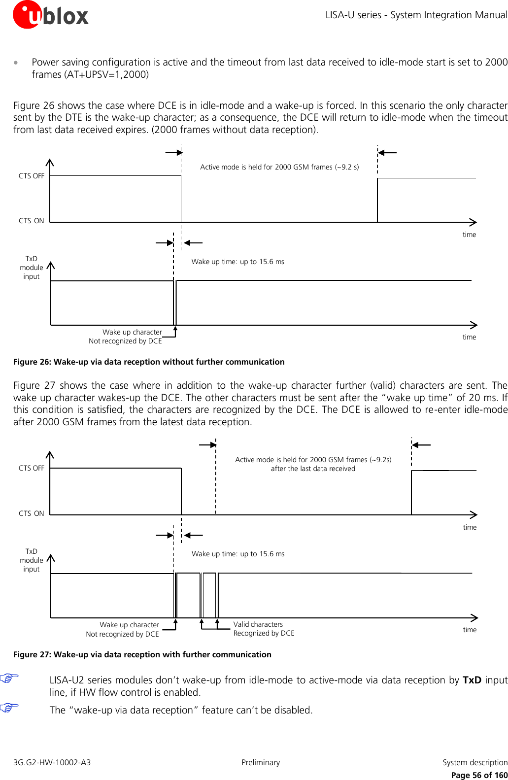
![LISA-U series - System Integration Manual 3G.G2-HW-10002-A3 Preliminary System description Page 57 of 160 The “wake-up via data reception” feature can be used in both +UPSV=1 and +UPSV=2 case (when RTS line is set to OFF). In command mode, if HW flow control is not implemented by the DTE, the DTE must always send a dummy “AT” to the module before each command line: the first character will not be ignored if the module is in active-mode (i.e. the module will reply “OK”), or it will represent the wake up character if the module is in idle-mode (i.e. the module won’t reply). No dummy “AT” is required from the DTE during connected-mode since the module continues to be in active-mode and doesn’t need to be woken-up. Furthermore in data mode a dummy “AT” would affect the data communication. 1.9.2.4 UART application circuits Providing the full RS-232 functionality (using the complete V.24 link) For complete RS-232 functionality conforming to ITU Recommendation [4] in DTE/DCE serial communication, the complete UART interface of the module (DCE) must be connected to a 1.8V DTE as described in Figure 28. TxDApplication Processor(1.8V DTE)RxDRTSCTSDTRDSRRIDCDGNDLISA-U series (DCE)15 TXD12 DTR16 RXD13 RTS14 CTS9DSR10 RI11 DCDGND0 Ω0 ΩTPTP0 Ω0 ΩTPTP Figure 28: UART interface application circuit with complete V.24 link in DTE/DCE serial communication (1.8V DTE)](https://usermanual.wiki/u-blox/LISAU230/User-Guide-1727756-Page-57.png)
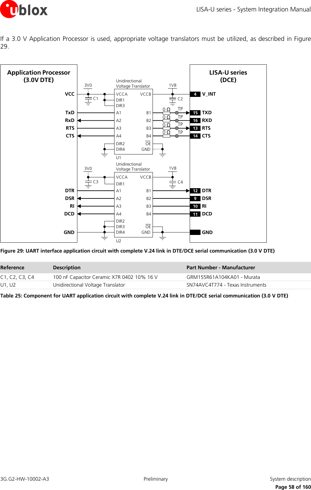
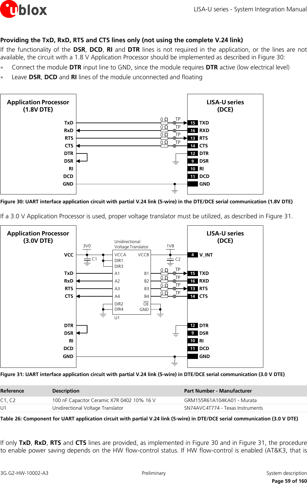
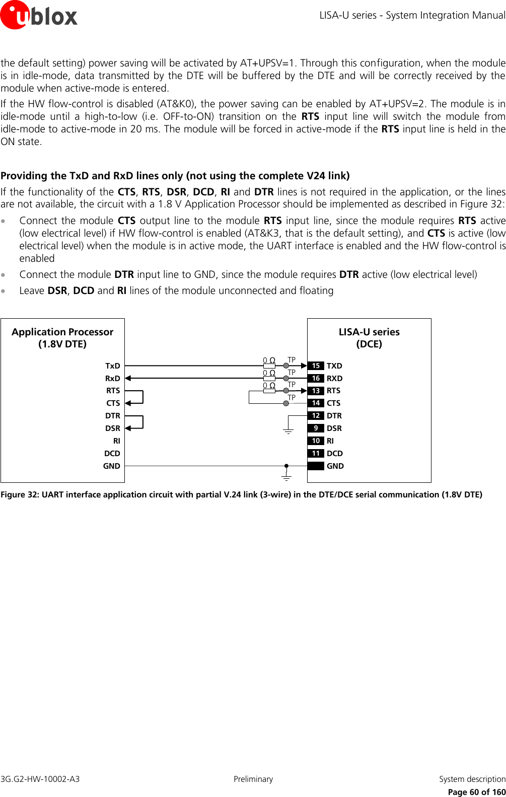
![LISA-U series - System Integration Manual 3G.G2-HW-10002-A3 Preliminary System description Page 62 of 160 Additional considerations If the module USB interface is connected to the application processor, it is highly recommended to provide direct access to RxD, TxD, CTS and RTS lines of the module for execution of firmware upgrade over UART and for debug purpose: testpoints can be added on the lines to accommodate the access and a 0 Ω series resistor must be mounted on each line to detach the module pin from any other connected device. Otherwise, if the USB interface is not connected to the application processor, it is highly recommended to provide direct access to VUSB_DET, USB_D+, USB_D- lines for execution of firmware upgrade over USB and for debug purpose. In both cases, provide as well access to RESET_N pin, or to the PWR_ON pin, or enable the DC supply connected to the VCC pin to start the module firmware upgrade (see Firmware Update Application Note [17]). If the UART interface is not used, all the UART interface pins can be left unconnected, but it is highly recommended to provide direct access to the RxD, TxD, CTS and RTS lines for execution of firmware upgrade and for debug purpose. Any external signal connected to the UART interface must be tri-stated when the module is in power-down mode, when the external reset is forced low and during the module power-on sequence (at least for 3 s after the start-up event), to avoid latch-up of circuits and allow a proper boot of the module. If the external signals connected to the wireless module cannot be tri-stated, insert a multi channel digital switch (e.g. Texas Instruments SN74CB3Q16244, TS5A3159, or TS5A63157) between the two-circuit connections and set to high impedance during module power down mode, when external reset is forced low and during power-on sequence. 1.9.3 USB interface LISA-U series modules provide a high-speed USB interface at 480 Mb/s compliant with the Universal Serial Bus Revision 2.0 specification [8]. It acts as a USB device and can be connected to any USB host such as a PC or other Application Processor. The USB-device shall look for all upper-SW-layers like any other serial device. This means that LISA-U series modules emulate all serial control logical lines. If the logical DTR line isn't enabled by the USB host, the LISA-U1xx-00 modules don’t answer to AT commands by the USB interface. Name Description Remarks VUSB_DET USB detect input Apply 5 V typical to enable USB USB_D+ USB Data Line D+ 90 Ω nominal differential impedance. Pull-up or pull-down resistors and external series resistors as required by the USB 2.0 high-speed specification [8] are part of the USB pad driver and need not be provided externally. USB_D- USB Data Line D- 90 Ω nominal differential impedance. Pull-up or pull-down resistors and external series resistors as required by the USB 2.0 high-speed specification [8] are part of the USB pad driver and need not be provided externally. Table 28: USB pins The USB interface pins ESD sensitivity rating is 1 kV (Human Body Model according to JESD22-A114F). Higher protection level could be required if the lines are externally accessible on the application board. Higher protection level can be achieved by mounting a very low capacitance (i.e. less or equal to 1 pF) ESD protection (e.g. Tyco Electronics PESD0402-140 ESD protection device) on the lines connected to these pins, close to accessible points.](https://usermanual.wiki/u-blox/LISAU230/User-Guide-1727756-Page-62.png)
![LISA-U series - System Integration Manual 3G.G2-HW-10002-A3 Preliminary System description Page 63 of 160 1.9.3.1 USB features LISA-U series modules simultaneously support 6 USB CDC (Communications Device Class) that assure multiple functionalities to the USB physical interface. The 6 available CDCs are configured as described in the following list: USB1: AT commands / data connection USB2: AT commands / data connection USB3: AT commands / data connection USB4: GPS tunneling dedicated port USB5: 2G and BB trace dedicated port USB6: 3G trace dedicated port All LISA-U2 series modules versions except LISA-U200-00 provide an additional USB CDC: USB7: SIM Access Profile dedicated port The user can concurrently use AT command interface on one CDC and Packet-Switched / Circuit-Switched Data communication on another CDC. All LISA-U2 series modules versions except LISA-U200-00 support audio over USB capabilities: Audio Device Class is implemented to provide an audio streaming interface, which transfers audio data over isochronous pipes. USB drivers for Windows XP, Windows Vista, Windows 7, Windows CE 6, Windows EC 7 and Windows Mobile 6.5 are available. LISA-U1 / LISA-U2 series modules are compatible with standard Linux/Android USB kernel drivers. LISA-U series module identifies itself by its VID (Vendor ID) and PID (Product ID) combination, included in the USB device descriptor. VID and PID of LISA-U series modules are the following: VID = 0x1546 PID = 0x1101 for LISA-U1 series PID = 0x1102 for LISA-U2 series If the USB interface of LISA-U series module is connected to the host before the module switch on, or if the module is reset with the USB interface connected to the host, the VID and PID are automatically updated runtime, after the USB detection. First, VID and PID are the following: VID = 0x058B PID = 0x0041 Then, after a time period (~5 s), VID and PID are updated to the following: VID = 0x1546 PID = 0x1101 for LISA-U1 series PID = 0x1102 for LISA-U2 series 1.9.3.2 USB and power saving If power saving is enabled by AT command (AT+UPSV=1 or AT+UPSV=2), the LISA-U series module automatically enters the USB suspended state when the device has observed no bus traffic for a specified period (refer to the Universal Serial Bus Revision 2.0 specification [8]). In suspended state, the module maintains any internal status as USB device, including its address and configuration. In addition, the module enters the suspended state when the hub port it is attached to is disabled: this is referred to as USB selective suspend. The module exits suspend mode when there is bus activity. LISA-U series module is capable of USB remote wake-up signaling: i.e. may request the host to exit suspend mode or selective suspend by using electrical signaling to indicate remote wake-up. This notifies the host that it](https://usermanual.wiki/u-blox/LISAU230/User-Guide-1727756-Page-63.png)
![LISA-U series - System Integration Manual 3G.G2-HW-10002-A3 Preliminary System description Page 64 of 160 should resume from its suspended mode, if necessary, and service the external event that triggered the suspended USB device to signal the host. Remote wake-up is accomplished using electrical signaling described in the Universal Serial Bus Revision 2.0 specification [8]. When the USB enters suspended state, the average VCC module current consumption of LISA-U series module is ~400 µA higher then when the USB is not attached to a USB host. If power saving is disabled by AT+UPSV=0 and the LISA-U series module is attached to a USB host as USB device, is configured and is not suspended, the average VCC module current consumption in fixed active mode is increased to ~40 mA. 1.9.3.3 USB application circuit Since the module acts as a USB device, the USB supply (5.0 V typ.) must be provided to VUSB_DET by the connected USB host. The USB interface is enabled only when a valid voltage as USB supply is detected by the VUSB_DET input. Neither the USB interface, nor the whole module is supplied by the VUSB_DET input: the VUSB_DET senses the USB supply voltage and absorbs few microamperes. The USB_D+ and USB_D- lines carry the USB serial data and signaling. The lines are used in single ended mode for relatively low speed signaling handshake, as well as in differential mode for fast signaling and data transfer. USB pull-up or pull-down resistors on pins USB_D+ and USB_D- as required by the Universal Serial Bus Revision 2.0 specification [8] are part of the USB pad driver and do not need to be externally provided. External series resistors on pins USB_D+ and USB_D- as required by the Universal Serial Bus Revision 2.0 specification [8] are also integrated: characteristic impedance of USB_D+ and USB_D- lines is specified by the USB standard. The most important parameter is the differential characteristic impedance applicable for odd-mode electromagnetic field, which should be as close as possible to 90 differential: signal integrity may be degraded if the PCB layout is not optimal, especially when the USB signaling lines are very long. LISA-U series VBUSD+D-GND18 VUSB_DET27 USB_D+26 USB_D-GNDC1USB DEVICE CONNECTORD1 D2 D3 Figure 34: USB Interface application circuit Reference Description Part Number - Manufacturer D1, D2, D3 Very Low Capacitance ESD Protection PESD0402-140 - Tyco Electronics C2 100 nF Capacitor Ceramic X7R 0402 10% 16 V GRM155R61A104KA01 - Murata Table 29: Component for USB application circuit If the USB interface is not connected to the application processor, it is highly recommended to provide direct access to the VUSB_DET, USB_D+, USB_D- lines for execution of firmware upgrade over USB and for debug purpose: testpoints can be added on the lines to accommodate the access. Otherwise, if the USB interface is connected to the application processor, it is highly recommended to provide direct access to the RxD, TxD, CTS and RTS lines for execution of firmware upgrade over UART and for debug purpose. In both cases, provide as well access to RESET_N pin, or to the PWR_ON pin, or enable the](https://usermanual.wiki/u-blox/LISAU230/User-Guide-1727756-Page-64.png)
![LISA-U series - System Integration Manual 3G.G2-HW-10002-A3 Preliminary System description Page 65 of 160 DC supply connected to the VCC pin to start the module firmware upgrade (see Firmware Update Application Note [17]). If the USB interface is not used, the USB_D+, USB_D- and VUSB_DET pins can be left unconnected, but it is highly recommended to provide direct access to the lines for execution of firmware upgrade and for debug purpose. 1.9.4 SPI interface SPI is a master-slave protocol: the module runs as an SPI slave, i.e. it accepts AT commands on its SPI interface without specific configuration. The SPI-compatible synchronous serial interface cannot be used for FW upgrade. The standard 3-wire SPI interface includes two signals to transmit and receive data (SPI_MOSI and SPI_MISO) and a clock signal (SPI_SCLK). LISA-U series modules provide two handshake signals (SPI_MRDY and SPI_SRDY), added to the standard 3-wire SPI interface, implementing the 5-wire Inter Processor Communication (IPC) interface. The purpose of the IPC interface is to achieve high speed communication (up to 26 Mb/s) between two processors following the same IPC specifications: the module baseband processor and an external processor. High speed communication is possible only if both sides follow the same Inter Processor Communication (IPC) specifications. Name Description Remarks SPI_MISO SPI Data Line. Master Input, Slave Output Module Output. Idle high. Shift data on rising clock edge (CPHA=1). Latch data on falling clock edge (CPHA=1). MSB is shifted first. SPI_MOSI SPI Data Line. Master Output, Slave Input Module Input. Idle high. Shift data on rising clock edge (CPHA=1). Latch data on falling clock edge (CPHA=1). MSB is shifted first. Internal active pull-up to V_INT (1.8 V) enabled. SPI_SCLK SPI Serial Clock. Master Output, Slave Input Module Input. Idle low (CPOL=0). Up to 26 MHz supported. Internal active pull-down to GND enabled. SPI_MRDY SPI Master Ready to transfer data control line. Master Output, Slave Input Module Input. Idle low. Internal active pull-down to GND enabled. SPI_SRDY SPI Slave Ready to transfer data control line. Master Input, Slave Output Module Output. Idle low. Table 30: SPI interface signals The SPI interface pins ESD sensitivity rating is 1 kV (Human Body Model according to JESD22-A114F). Higher protection level could be required if the lines are externally accessible on the application board. Higher protection level can be achieved by mounting a low capacitance (i.e. less than 10 pF) ESD protection (e.g. AVX USB0002 varistor array) on the lines connected to these pins, close to accessible points.](https://usermanual.wiki/u-blox/LISAU230/User-Guide-1727756-Page-65.png)
![LISA-U series - System Integration Manual 3G.G2-HW-10002-A3 Preliminary System description Page 68 of 160 3. The master activates the clock and the two processors exchange the communication header and data 4. If the data has been exchanged, the slave deactivates SPI_SRDY to process the received information. The master does not need to de-assert SPI_MRDY as it controls the SPI_SCLK 5. After the preparation, the slave activates again SPI_SRDY and wait for SPI_SCLK activation. When the clock is active, all data is transferred without intervention. If there is more data to transfer (flag set in any of the headers), the process will repeat from step 3 Slave ended transfer Figure 38: Data transfer terminated and then restarted by LISA-U series module (slave) Starting from the state where data transfer is ongoing, the following actions will happen: 1. In case of the last transfer, the master will lower its SPI_MRDY line. After the data-transfer is finished the line must be low. If the slave has already set its SPI_SRDY line, the master must raise its line to initiate the next transfer (slave-waking-procedure) 2. If the data has been exchanged, the slave will deactivate SPI_SRDY to process the received information. This is the normal behavior 3. The slave will indicate the master that is ready to send data by activating SPI_SRDY 4. When the master is ready to send, it will signalize this by activating SPI_MRDY. This is optional, when SPI_MRDY is low before 5. The slave indicates immediately after a transfer termination that it is ready to start transmission again. In this case the slave will raise SPI_SRDY again. The SPI_MRDY line can be either high or low: the master has only to ensure that the SPI_SRDY change will be detected correctly via interrupt For more details regarding IPC communication protocol please refer to SPI Application Note [18]. 1.9.4.4 IPC application circuit SPI_MOSI is the data line input for the module since it runs as SPI slave: it must be connected to the data line output (MOSI) of the application processor that runs as an SPI master. SPI_MISO is the data line output for the module since it runs as SPI slave: it must be connected to the data line input (MISO) of the application processor that runs as an SPI master. SPI_SCLK is the clock input for the module since it runs as SPI slave: it must be connected to the clock line output (SCLK) of the application processor that runs as an SPI master. SPI_MRDY is an input for the module able to detect an external interrupt which comes from the application processor. SPI_SRDY is an output for the module, and the application processor should be able to detect an external interrupt which comes from the module on its connected pin. Signal integrity of the high speed data lines may be degraded if the PCB layout is not optimal, especially when the SPI lines are very long: keep routing short and minimize parasitic capacitance to preserve signal integrity. SPI_MRDY SPI_SRDY DATA EXCHG 5 2 1 Header Data 3 4](https://usermanual.wiki/u-blox/LISAU230/User-Guide-1727756-Page-68.png)
![LISA-U series - System Integration Manual 3G.G2-HW-10002-A3 Preliminary System description Page 69 of 160 LISA-U series(SPI slave)MOSIApplication Processor(SPI master)MISOSCLKInterruptGPIOGND56 SPI_MOSI59 SPI_MRDY57 SPI_MISO55 SPI_SCLK58 SPI_SRDYGND Figure 39: IPC Interface application circuit If direct access to the USB or the UART interfaces of the module is not provided, it is recommended to provide direct access to the SPI_MOSI, SPI_MISO, SPI_SCLK, SPI_MRDY, SPI_SRDY lines of the module for debug purpose: testpoints can be added on the lines to accommodate the access and a 0 Ω series resistor must be mounted on each line to detach the module pin from any other connected device. If the SPI/IPC interface is not used, the SPI_MOSI, SPI_MISO, SPI_SCLK, SPI_MRDY, SPI_SRDY pins can be left unconnected. Any external signal connected to the SPI / IPC interface must be tri-stated when the module is in power-down mode, when the external reset is forced low and during the module power-on sequence (at least for 3 s after the start-up event), to avoid latch-up of circuits and allow a proper boot of the module. If the external signals connected to the wireless module cannot be tri-stated, insert a multi channel digital switch (e.g. Texas Instruments SN74CB3Q16244, TS5A3159, or TS5A63157) between the two-circuit connections and set to high impedance during module power down mode, when external reset is forced low and during power-on sequence. 1.9.5 MUX Protocol (3GPP 27.010) LISA-U series modules have a software layer with MUX functionality, 3GPP TS 27.010 Multiplexer Protocol [7], available either on the UART or on the SPI physical link. The USB interface doesn’t support the multiplexer protocol. This is a data link protocol (layer 2 of OSI model) which uses HDLC-like framing and operates between the module (DCE) and the application processor (DTE) and allows a number of simultaneous sessions over the used physical link (UART or SPI): the user can concurrently use AT command interface on one MUX channel and Packet-Switched / Circuit-Switched Data communication on another MUX channel. The multiplexer protocol can be used on one serial interface (UART or SPI) at a time. Each session consists of a stream of bytes transferring various kinds of data such as SMS, CBS, PSD, GPS, AT commands in general. This permits, for example, SMS to be transferred to the DTE when a data connection is in progress. The following virtual channels are defined: Channel 0: control channel Channel 1 – 5: AT commands /data connection Channel 6: GPS tunneling All LISA-U2 series modules versions except LISA-U200-00 provide an additional channel: Channel 7: SIM Access Profile dedicated port For more details please refer to GSM Mux implementation Application Note [15].](https://usermanual.wiki/u-blox/LISAU230/User-Guide-1727756-Page-69.png)
![LISA-U series - System Integration Manual 3G.G2-HW-10002-A3 Preliminary System description Page 70 of 160 1.10 DDC (I2C) interface 1.10.1 Overview An I2C compatible Display Data Channel (DDC) interface for communication with u-blox GPS receivers is available on LISA-U series modules. The communication between a u-blox wireless module and a u-blox GPS receiver is only provided by this DDC (I2C) interface. Name Description Remarks SCL I2C bus clock line Open drain. External pull-up required. SDA I2C bus data line Open drain. External pull-up required. Table 31: DDC pins The DDC (I2C) interface pins ESD sensitivity rating is 1 kV (HBM according to JESD22-A114F). Higher protection level could be required if the lines are externally accessible on the application board. Higher protection level can be achieved by mounting an ESD protection (e.g. EPCOS CA05P4S14THSG varistor array) on the lines connected to these pins, close to accessible points. u-blox has implemented special features in LISA-U series wireless modules to ease the design effort required for the integration of a u-blox wireless module with a u blox GPS receiver. Combining a u-blox wireless module with a u-blox GPS receiver allows designers to have full access to the GPS receiver directly via the wireless module: it relays control messages to the GPS receiver via a dedicated DDC (I2C) interface. A 2nd interface connected to the GPS receiver is not necessary: AT commands via the UART serial interface of the wireless module allows a fully control of the GPS receiver from any host processor. LISA-U series modules feature embedded GPS aiding that is a set of specific features developed by u-blox to enhance GPS performance, decreasing Time To First Fix (TTFF), thus allowing to calculate the position in a shorter time with higher accuracy. The DDC (I2C) interface of all LISA-U2 series modules versions except LISA-U200-00 can be used to communicate with u-blox GPS receivers and at the same time to control an external audio codec: the LISA-U2 series module acts as an I2C master which can communicate to two I2C slaves as allowed by the I2C bus specifications. Refer to section 1.11.2 for an application circuit with an external audio codec. LISA-U200-00 modules versions don’t support an I2C compatible Display Data Channel (DDC) interface for communication with u-blox GPS receivers and don’t feature embedded GPS aiding. For more details regarding the handling of the DDC (I2C) interface and the GPS aiding features please refer to u-blox AT Commands Manual [3] (AT+UGPS, AT+UGPRF, AT+UGPIOC commands) and GPS Implementation Application Note [16]. 1.10.2 DDC application circuit The DDC (I2C) interface of LISA-U series modules is used to connect the wireless module to a u-blox GPS receiver: the communication with the u-blox GPS receiver by DDC (I2C) interface is enabled by the AT+UGPS command (for more details refer to u-blox AT Commands Manual [3]). The SDA and SCL lines must be connected to the DDC (I2C) interface pins of the u-blox GPS receiver (i.e. the SDA2 and SCL2 pins of the u-blox GPS receiver) on the application board to allow the communication between the wireless module and the u-blox GPS receiver. To be compliant to the I2C bus specifications, the module bus interface pads are open drain output and pull up resistors must be used. Since the pull-up resistors are not mounted on the module, they must be mounted](https://usermanual.wiki/u-blox/LISAU230/User-Guide-1727756-Page-70.png)
![LISA-U series - System Integration Manual 3G.G2-HW-10002-A3 Preliminary System description Page 71 of 160 externally. Resistor values must conform to the I2C bus specifications [9]. If a LISA-U series module is connected by the DDC (I2C) bus to a u-blox GPS receiver (only one device can be connected on the DDC bus), use a pull-up resistor of 4.7 k. Pull-ups must be connected to a supply voltage of 1.8 V (typical), since this is the voltage domain of the DDC pins. V_INT digital interfaces supply output can be used to provide 1.8 V for the pull-ups (for detailed electrical characteristics see LISA-U1 series Data Sheet [1] and LISA-U2 series Data Sheet [2]). DDC Slave-mode operation is not supported, the module can act as master only. Two lines, serial data (SDA) and serial clock (SCL), carry information on the bus. SCL is used to synchronize data transfers, and SDA is the data line. Since both lines are open drain outputs, the DDC devices can only drive them low or leave them open. The pull-up resistor pulls the line up to the supply rail if no DDC device is pulling it down to GND. If the pull-ups are missing, SCL and SDA lines are undefined and the DDC bus will not work. The signal shape is defined by the values of the pull-up resistors and the bus capacitance. Long wires on the bus will increase the capacitance. If the bus capacitance is increased, use pull-up resistors with nominal resistance value lower than 4.7 k, to match the I2C bus specifications [9].regarding rise and fall times of the signals. Capacitance and series resistance must be limited on the bus to match the I2C specifications (1.0 µs is the maximum allowed rise time on the SCL and SDA lines): route connections as short as possible. If the pins are not used as DDC bus interface, they can be left unconnected. LISA-U series modules support these GPS aiding types: Local aiding AssistNow Online AssistNow Offline AssistNow Autonomous The embedded GPS aiding features can be used only if the DDC (I2C) interface of the wireless module is connected to the u-blox GPS receivers. The GPIO pins can handle: GPS receiver power-on/off (“GPS supply enable” function provided by GPIO2) The wake up from idle-mode when the GPS receiver is ready to send data (“GPS data ready” function provided by GPIO3) The RTC synchronization signal to the GPS receiver (“GPS RTC sharing” function provided by GPIO4) LISA-U1xx-00 modules versions don’t support the following further features related to GPS functionality: o LISA-U1xx-00 modules versions don’t enter idle-mode when the DDC (I2C) interface is enabled by the AT+UGPS command, even if power saving is enabled by the AT+UPSV command o LISA-U1xx-00 modules versions don’t support “GPS data ready” and “GPS RTC sharing” functions o LISA-U1xx-00 modules versions don’t support AssistNow Autonomous GPS aiding The GPIO2 is by default configured to provide the “GPS supply enable” function (parameter <gpio_mode> of AT+UGPIOC command set to 3 by default), to enable or disable the supply of the u-blox GPS receiver connected to the wireless module by the AT+UGPS command. The pin is set as Output / High, to switch on the u-blox GPS receiver, if the parameter <mode> of AT+UGPS command is set to 1 Output / Low, to switch off the u-blox GPS receiver, if the parameter <mode> of AT+UGPS command is set to 0 (default setting) The pin must be connected to the active-high enable pin (or the active-low shutdown pin) of the voltage regulator that supplies the u-blox GPS receiver on the application board.](https://usermanual.wiki/u-blox/LISAU230/User-Guide-1727756-Page-71.png)
![LISA-U series - System Integration Manual 3G.G2-HW-10002-A3 Preliminary System description Page 73 of 160 “GPS data ready” and “GPS RTC sharing” functions are not supported by all u-blox GPS receivers HW or ROM/FW versions. Refer to the GPS Implementation Application Note [16] or to the Hardware Integration Manual of the u-blox GPS receivers for the supported features. Functions not supported by LISA-Uxxx-00 versionsLISA-U seriesR1INOUTGNDGPS LDORegulatorSHDNu-blox1.8 V GPS receiverSDA2SCL2R21V8 1V8VMAIN1V8U121 GPIO2SDASCLC1TxD1EXTINT0GPIO3GPIO446452324VCCR3V_BCKP V_BCKP2Functions not supported by LISA-U200-00 version Figure 40: DDC Application circuit for u-blox 1.8 V GPS receiver Reference Description Part Number - Manufacturer R1, R2 4.7 kΩ Resistor 0402 5% 0.1 W RC0402JR-074K7L - Yageo Phycomp R3 47 kΩ Resistor 0402 5% 0.1 W RC0402JR-0747KL - Yageo Phycomp U1 Voltage Regulator for GPS Receiver See GPS Receiver Hardware Integration Manual Table 32: Components for DDC application circuit for u-blox 1.8 V GPS receiver The application circuit for the connection of a LISA-U series wireless module to a u-blox 3.0 V GPS receiver is illustrated in Figure 41. If a u-blox 3 V GPS receiver is used, the SDA, SCL, GPIO3 and GPIO4 pins of the LISA-U series wireless module cannot be directly connected to the u-blox 3 V GPS receiver: a proper I2C-bus Bidirectional Voltage Translator must be used for the SDA and SCL signals, and a general purpose Voltage Translator must be used for the GPIO3 and GPIO4 signals. The V_BCKP supply output of the wireless module can be directly connected to the V_BCKP backup supply input pin of the GPS receiver as in the application circuit for a u-blox 1.8 V GPS receiver.](https://usermanual.wiki/u-blox/LISAU230/User-Guide-1727756-Page-73.png)
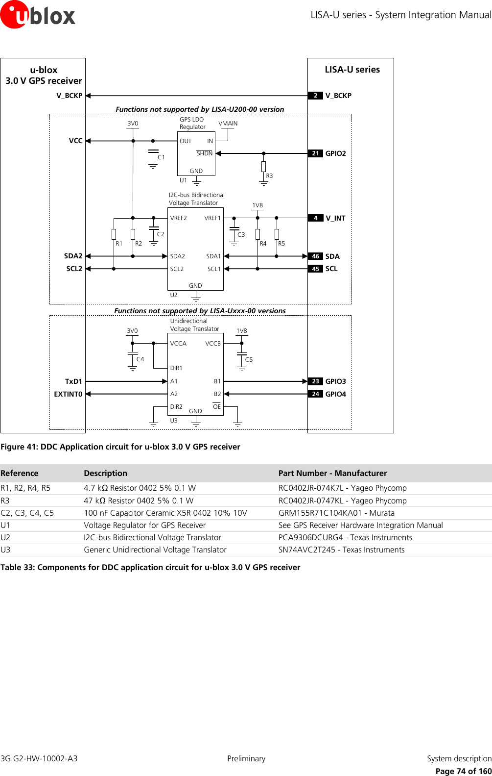
![LISA-U series - System Integration Manual 3G.G2-HW-10002-A3 Preliminary System description Page 75 of 160 1.11 Audio Interface LISA-U120 and LISA-U130 modules provide analog and digital input/output audio interfaces: Differential analog audio input (MIC_P, MIC_N) and differential analog audio output (SPK_P, SPK_N) 4-wire I2S digital audio interface (I2S_CLK, I2S_RXD, I2S_TXD and I2S_WA) All LISA-U2 series modules versions except LISA-U200-00 provide two digital input/output audio interfaces: First 4-wire I2S digital audio interface (I2S_CLK, I2S_RXD, I2S_TXD and I2S_WA) Second 4-wire I2S digital audio interface (I2S1_CLK, I2S1_RXD, I2S1_TXD and I2S1_WA) Audio signal routing can be controlled by the dedicated AT command +USPM (refer to u-blox AT Commands Manual [3]). This command allows setting the audio path mode, composed by the uplink audio path and the downlink audio path. Each uplink path mode defines the physical input (i.e. the analog or the digital audio input) and the set of parameters to process the uplink audio signal (uplink gains, uplink digital filters, echo canceller parameters). For example the “Headset microphone” uplink path uses the differential analog audio input with the default parameters for the headset profile. Each downlink path mode defines the physical output (i.e. the analog or the digital audio output) and the set of parameters to process the downlink audio signal (downlink gains, downlink digital filters and sidetone). For example the “Mono headset” downlink path uses the differential analog audio output with the default parameters for the headset profile. The set of parameters to process the uplink or the downlink audio signal can be changed with dedicated AT commands for each uplink or downlink path and then stored in two profiles in the non volatile memory (refer to u-blox AT Commands Manual [3] for Audio parameters tuning commands). 1.11.1 Analog Audio interface LISA-U100, LISA-U110 and LISA-U2 series modules versions don’t support analog audio interface. 1.11.1.1 Uplink path (differential analog audio input) The pins related to the differential analog audio input are: MIC_P / MIC_N: Differential analog audio signal inputs (positive/negative). These two pins are provided with internal series 100 nF capacitors for DC blocking that connect the module pads to the differential input of a Low Noise Amplifier. The LNA output is internally connected to the digital processing system by an integrated sigma-delta analog-to-digital converter The analog audio input is selected when the parameter <main_uplink> in AT+USPM command is set to “Headset microphone”, “Handset microphone” or “Hands-free microphone”: the uplink analog path profiles use the same physical input but have different sets of audio parameters (for more details please refer to u-blox AT Commands Manual [3], AT+USPM, AT+UMGC, AT+UUBF, AT+UHFP commands). There is no microphone supply pin available on the module: an external low noise LDO voltage regulator should be added to provide a proper supply for a microphone. Detailed electrical characteristics of the differential analog audio input can be found in the LISA-U1 series Data Sheet [1].](https://usermanual.wiki/u-blox/LISAU230/User-Guide-1727756-Page-75.png)
![LISA-U series - System Integration Manual 3G.G2-HW-10002-A3 Preliminary System description Page 76 of 160 1.11.1.2 Downlink path (differential analog audio output) The pins related to the differential analog audio output are: SPK_P / SPK_N: Differential analog audio signal output (positive/negative). These two pins are internally directly connected to the differential output of a low power audio amplifier, for which the input is internally connected to the digital processing system by to an integrated digital-to-analog converter The analog audio output is selected when the parameter <main_downlink> in AT+USPM command is set to “Normal earpiece”, “Mono headset” or “Loudspeaker”: the downlink analog path profiles use the same physical output but have different sets of audio parameters (for more details please refer to u-blox AT Commands Manual [3], AT+USPM, AT+USGC, AT+UDBF, AT+USTN commands). The differential analog audio output can be directly connected to a headset earpiece or handset earpiece but is not able to drive an 8 speaker. Detailed electrical characteristics of the differential audio output can be found in LISA-U1 series Data Sheet [1]. Warning: excessive sound pressure from headphones can cause hearing loss. Table 34 lists the signals related to analog audio functions. Name Module Description Remarks MIC_P LISA-U120 LISA-U130 Differential analog audio input (Positive) Shared for all uplink analog path modes: handset, headset, hands-free mode. Internal DC blocking capacitor. MIC_N LISA-U120 LISA-U130 Differential analog audio input (Negative) Shared for all uplink analog path modes: handset, headset, hands-free mode. Internal DC blocking capacitor. SPK_P LISA-U120 LISA-U130 Differential analog audio output (Positive) Shared for all uplink analog path modes: earpiece, headset, loudspeaker mode. SPK_N LISA-U120 LISA-U130 Differential analog audio output (Negative) Shared for all uplink analog path modes: earpiece, headset, loudspeaker mode. Table 34: Analog audio interface pins The audio pins ESD sensitivity rating is 1 kV (Human Body Model according to JESD22-A114F). Higher protection level could be required if the lines are externally accessible on the application board. Higher protection level can be achieved by mounting an ESD protection (e.g. EPCOS CA05P4S14THSG varistor array) on the lines connected to these pins, close to accessible points. All corresponding differential audio lines must be routed in pairs, be embedded in GND (have the ground lines as close as possible to the audio lines), and maintain distance from noisy lines such as VCC and from components such as switching regulators. If the audio pins are not used, they can be left unconnected on the application board. 1.11.1.3 Headset mode Headset mode is the default audio operating mode of the LISA-U120 and LISA-U130 modules. The headset profile is configured when the uplink audio path is set to “Headset microphone” and the downlink audio path is set to “Mono headset” (refer to u-blox AT Commands Manual [3]: AT+USPM command: <main_uplink>, <main_downlink> parameters): Headset microphone must be connected to the module differential input MIC_P / MIC_N Headset receiver must be connected to the module differential output SPK_P / SPK_N](https://usermanual.wiki/u-blox/LISAU230/User-Guide-1727756-Page-76.png)
![LISA-U series - System Integration Manual 3G.G2-HW-10002-A3 Preliminary System description Page 77 of 160 Figure 42 shows an example of an application circuit connecting a headset (with a 2.2 k electret microphone and a 32 receiver) to the LISA-U120 and LISA-U130 modules, with an external low noise LDO voltage regulator to provide a proper supply for the microphone. Mount an 82 nH series inductor (e.g. Murata LQG15HS82NJ02) on each microphone line, and a 27 pF bypass capacitor (e.g. Murata GRM1555C1H270J) on all audio lines to minimize RF coupling and TDMA noise. The physical width of the audio outputs lines on the application board must be wide enough to minimize series resistance. LISA-U120/U130C2 C3 C4J1253461L254SPK_N53SPK_P39MIC_N40MIC_PD1AUDIO HEADSET CONNECTORD2INOUTGNDLow Noise LDO Regulator VMAINU1R4R1C6R3R2 C52V5Sense lines connected to GND in one star pointL1C1C7 Figure 42: Headset mode application circuit Reference Description Part Number – Manufacturer C1, C2, C3, C4 27 pF Capacitor Ceramic COG 0402 5% 25 V GRM1555C1H270JA01 – Murata C5, C6, C7 10 µF Capacitor Ceramic X5R 0603 20% 6.3 V GRM188R60J106ME47 – Murata D1, D2 Low Capacitance ESD Protection USB0002RP or USB0002DP – AVX L1, L2 82 nH Multilayer inductor 0402 (self resonance frequency ~1 GHz) LQG15HS82NJ02 – Murata J1 Audio Headset 2.5 mm Jack Connector SJ1-42535TS-SMT – CUI, Inc. R1, R2, R3, R4 2.2 kΩ Resistor 0402 5% 0.1 W RC0402JR-072K2L – Yageo Phycomp U1 Low Noise LDO Linear Regulator 2.5 V 300 mA LT1962EMS8-2.5#PBF- Linear Technology Table 35: Example of components for headset jack connection 1.11.1.4 Handset mode The handset profile is configured when the uplink audio path is set to “Handset microphone” and the downlink audio path is set to “Normal earpiece” (refer to u-blox AT commands manual [3]: AT+USPM command: <main_uplink>, <main_downlink> parameters): Handset microphone must be connected to the module differential input MIC_P / MIC_N Handset receiver must be connected to the module differential output SPK_P / SPK_N](https://usermanual.wiki/u-blox/LISAU230/User-Guide-1727756-Page-77.png)
![LISA-U series - System Integration Manual 3G.G2-HW-10002-A3 Preliminary System description Page 78 of 160 Figure 43 shows an example of an application circuit connecting a handset (with a 2.2 k electret microphone and a 32 receiver) to the LISA-U120 and LISA-U130 modules, with an external low noise LDO voltage regulator to provide a proper supply for the microphone. Mount an 82 nH series inductor (e.g. Murata LQG15HS82NJ02) on each microphone line and a 27 pF bypass capacitor (e.g. Murata GRM1555C1H270J) on all audio lines to minimize RF coupling and TDMA noise. The physical width of the audio outputs lines on the application board must be wide enough to minimize series resistance. LISA-U120/U130C1 C2 C3 J14321L153SPK_P54SPK_N40MIC_P39MIC_ND1AUDIO HANDSET CONNECTORD2INOUTGNDLow Noise LDO RegulatorU1R4R1C6R3R2 C52V5Sense lines connected to GND in one star pointC4L2VMAINC7 Figure 43: Handset mode application circuit Reference Description Part Number – Manufacturer C1, C2, C3, C4 27 pF Capacitor Ceramic COG 0402 5% 25 V GRM1555C1H270JA01 – Murata C5, C6, C7 10 µF Capacitor Ceramic X5R 0603 20% 6.3 V GRM188R60J106ME47 – Murata D1, D2 Low Capacitance ESD Protection USB0002RP or USB0002DP – AVX L1, L2 82nH Multilayer inductor 0402 (self resonance frequency ~1 GHz) LQG15HS82NJ02 – Murata J1 Audio Handset Jack Connector, 4Ckt (4P4C) 52018-4416 – Molex R1, R2, R3, R4 2.2 kΩ Resistor 0402 5% 0.1 W RC0402JR-072K2L – Yageo Phycomp U1 Low Noise LDO Linear Regulator 2.5 V 300 mA LT1962EMS8-2.5#PBF- Linear Technology Table 36: Example of components for handset connection 1.11.1.5 Hands-free mode The hands-free profile is configured when the uplink audio path is set to “Hands-free microphone” and the downlink audio path is set to “Loudspeaker” (refer to u-blox AT commands manual [3]: AT+USPM command: <main_uplink>, <main_downlink> parameters): Hands-free microphone signal must be connected to the module differential input MIC_P / MIC_N High power loudspeaker must be connected to the output of an external audio amplifier, for which the input must be connected to the module differential output SPK_P / SPK_N The module differential analog audio output is not able to drive an 8 speaker: an external audio amplifier must be provided on the application board to amplify the low power audio signal provided by the module differential output SPK_P / SPK_N.](https://usermanual.wiki/u-blox/LISAU230/User-Guide-1727756-Page-78.png)
![LISA-U series - System Integration Manual 3G.G2-HW-10002-A3 Preliminary System description Page 79 of 160 Hands-free functionality is implemented using appropriate digital signal processing algorithms for voice-band handling (echo canceller and automatic gain control), managed via software (refer to u-blox AT commands manual [3], AT+UHFP command). Figure 43 shows an example of an application circuit connecting a 2.2 k electret microphone and an 8 speaker to the LISA-U120 and LISA-U130 modules, with an external low noise LDO voltage regulator to provide a proper supply for the microphone and with an external audio amplifier to amplify the low power audio signal provided by the module differential output. Mount an 82 nH series inductor (e.g. Murata LQG15HS82NJ02) on each microphone line and a 27 pF bypass capacitor (e.g. Murata GRM1555C1H270J) on all audio lines to minimize RF coupling and TDMA noise. The physical width of the audio outputs lines on the application board must be wide enough to minimize series resistance. C1 C2C3L139MIC_N53SPK_P40MIC_P54SPK_ND1Microphone ConnectorD2INOUTGNDLow Noise LDO RegulatorU1R4R1C6R3R2 C52V5Sense lines connected to GND in one star pointC4SPKL2MICSpeaker ConnectorOUT+IN+GNDVMAINU2OUT-IN-C8C9R5R6VDDC11C10LISA-U120/U130Audio AmplifierJ1J2VMAINC7 Figure 44: Hands-free mode application circuit Reference Description Part Number – Manufacturer C1, C2, C3, C4 27 pF Capacitor Ceramic COG 0402 5% 25 V GRM1555C1H270JZ01 – Murata C5, C6, C7, C10 10 µF Capacitor Ceramic X5R 0603 20% 6.3 V GRM188R60J106ME47 – Murata C8, C9 47 nF Capacitor Ceramic X7R 0402 10% 16V GRM155R71C473KA01 – Murata C11 100 nF Capacitor Ceramic X5R 0402 10% 10V GRM155R71C104KA01 – Murata D1, D2 Low Capacitance ESD Protection USB0002RP or USB0002DP – AVX J1 Microphone Connector J2 Speaker Connector L1, L2 82nH Multilayer inductor 0402 (self resonance frequency ~1 GHz) LQG15HS82NJ02 – Murata MIC 2.2 k Electret Microphone](https://usermanual.wiki/u-blox/LISAU230/User-Guide-1727756-Page-79.png)
![LISA-U series - System Integration Manual 3G.G2-HW-10002-A3 Preliminary System description Page 80 of 160 Reference Description Part Number – Manufacturer R1, R2, R3, R4 2.2 kΩ Resistor 0402 5% 0.1 W RC0402JR-072K2L – Yageo Phycomp R5, R6 0 Ω Resistor 0402 5% 0.1 W RC0402JR-070RL – Yageo Phycomp SPK 8 Loudspeaker U1 Low Noise LDO Linear Regulator 2.5 V 300 mA LT1962EMS8-2.5#PBF- Linear Technology U2 Filter-less Mono 2.8 W Class-D Audio Amplifier SSM2305CPZ – Analog Devices Table 37: Example of components for hands-free connection 1.11.1.6 Connection to an external analog audio device The differential analog audio input / output can be used to connect the module to an external analog audio device. Audio devices with a differential analog input / output are preferable, as they are more immune to external disturbances. If the external analog audio device is provided with a differential analog audio input, the SPK_P / SPK_N balanced output of the module must be connected to the differential input of the external audio device through a DC-block 10 µF series capacitor (e.g. Murata GRM188R60J106M) to decouple the bias present at the module output (see SPK_P / SPK_N common mode output voltage in the LISA-U1 series Data Sheet [1]). Use a suitable power-on sequence to avoid audio bump due to charging of the capacitor: the final audio stage should be always enabled as last one. If the external analog audio device is provided with a single ended analog audio input, a proper differential to single ended circuit must be inserted from the SPK_P / SPK_N balanced output of the module to the single ended input of the external audio device. A simple application circuit is described in Figure 45: 10 µF series capacitors (e.g. Murata GRM188R60J106M) are provided to decouple the bias present at the module output, and a voltage divider is provided to properly adapt the signal level from the module output to the external audio device input. The DC-block series capacitor acts as high-pass filter for audio signals, with cut-off frequency depending on both the values of capacitor and on the input impedance of the external audio device. For example: in case of differential input impedance of 600 , the two 10 µF capacitors will set the -3 dB cut-off frequency to 53 Hz, while for single ended connection to 600 external device, the cut-off frequency with just the single 10 µF capacitor will be 103 Hz. In both cases the high-pass filter has a low enough cut-off to not impact the audio signal frequency response. The signal levels can be adapted by setting gain using AT commands, but additional circuitry must be inserted if the SPK_P / SPK_N output level of the module is too high for the input of the audio device. If the external analog audio device is provided with a differential analog audio output, the MIC_P / MIC_N balanced input of the module must be connected directly to the differential output of the external audio device. Series capacitors are not needed since MIC_P / MIC_N pins are provided with internal 100 nF capacitors for DC blocking (see LISA-U1 series Data Sheet [1]). If the external analog audio device is provided with a single ended analog audio output, a proper single ended to differential circuit has to be inserted from the single ended output of the external audio device to the MIC_P / MIC_N balanced input of the module. A simple application circuit is described in Figure 45: a voltage divider is provided to properly adapt the signal level from the external audio device output to the module input. The signal levels can be adapted by setting gain using AT commands, but additional circuitry must be inserted if the output level of the audio device is too high for MIC_P / MIC_N. Please refer to Figure 45 for the application circuits. To enable the audio path corresponding to the differential analog audio input / output, please refer to u-blox AT Commands Manual [3]: AT+USPM command. To tune audio levels for the external device please refer to u-blox AT Commands Manual [3] (AT+USGC, AT+UMGC commands).](https://usermanual.wiki/u-blox/LISAU230/User-Guide-1727756-Page-80.png)
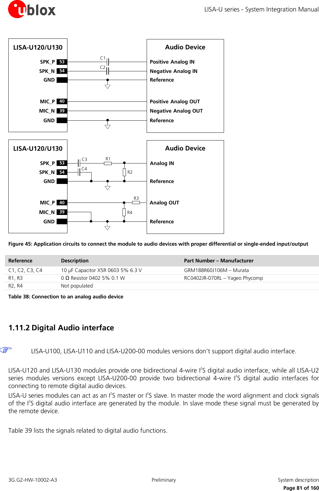
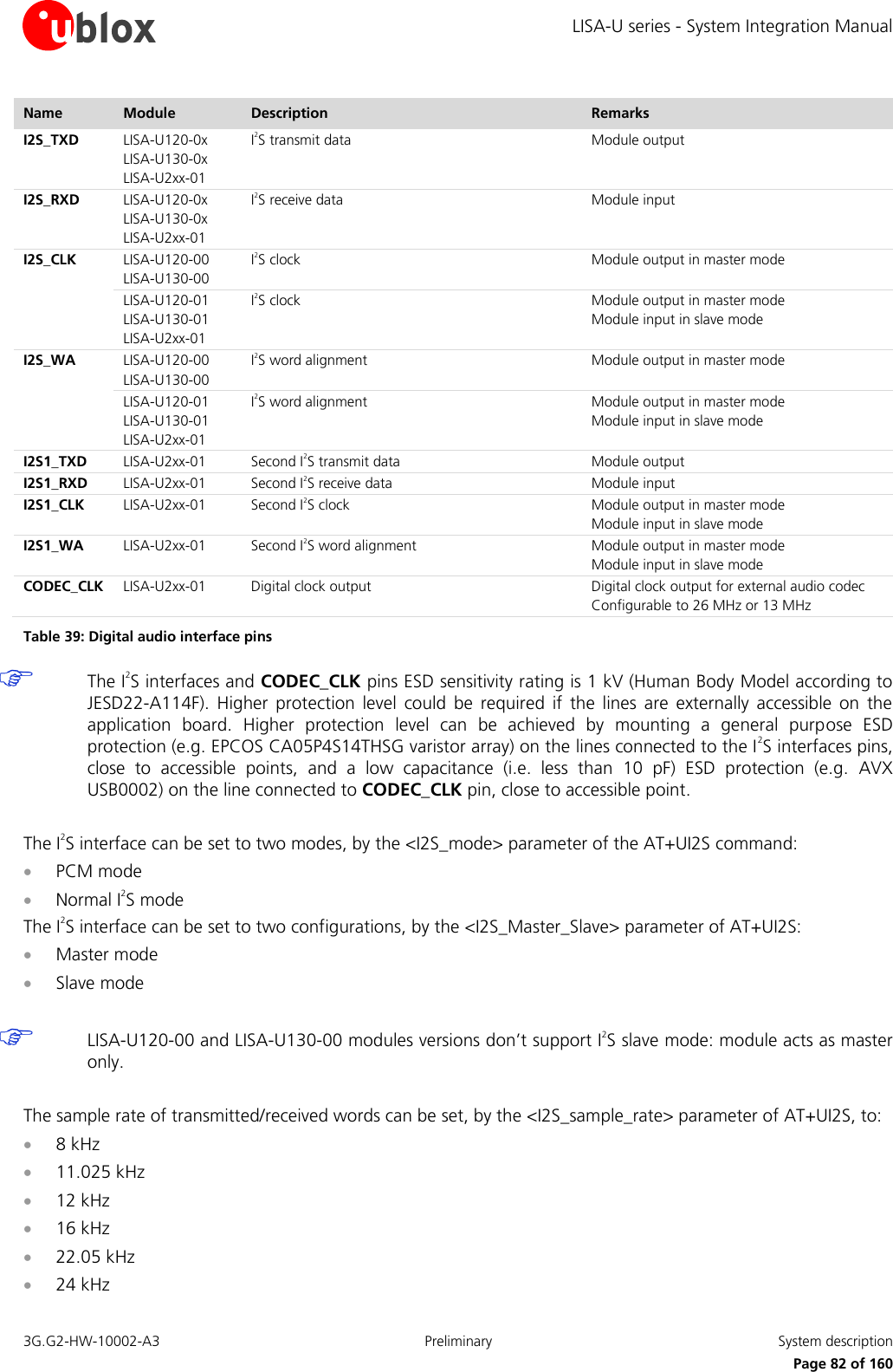
![LISA-U series - System Integration Manual 3G.G2-HW-10002-A3 Preliminary System description Page 83 of 160 32 kHz 44.1 kHz 48 kHz The sample rate of transmitted and received words of LISA-U120-00 and LISA-U130-00 modules cannot be configured: the sample rate is fixed at 8 kHz only. The <main_uplink> and <main_downlink> parameters of the AT+USPM command must be properly configured to select the I2S digital audio interfaces paths (for more details please refer to u-blox AT Commands Manual [3]): <main_uplink> has to be properly set to select: o the first I2S interface (using I2S_RXD module input) o the second I2S interface (using I2S1_RXD module input) <main_downlink> has to be properly set to select: o the first I2S interface (using I2S_TXD module output) o the second I2S interface (using I2S1_TXD module output) Parameters of digital path can be configured and saved as the normal analog paths, using appropriate path parameter as described in the u-blox AT Commands Manual [3], +USGC, +UMGC, +USTN AT command. Analog gain parameters of microphone and speakers are not used when digital path is selected. The I2S receive data input and the I2S transmit data output signals are respectively connected in parallel to the analog microphone input and speaker output signals, so resources available for analog path can be shared: Digital filters and digital gains are available in both uplink and downlink direction. They can be properly configured by the AT commands Ringer tone and service tone are mixed on the TX path when active (downlink) The HF algorithm acts on I2S path Refer to the u-blox AT Commands Manual [3]: AT+UI2S command for possible settings of I2S interface. 1.11.2.1 I2S interface - PCM mode Main features of the I2S interface in PCM mode: I2S runs in PCM - short alignment mode (configurable by AT commands) I2S word alignment signal can be configured to 8, 11.025, 12, 16, 22.05, 24, 32, 44.1, 48 kHz I2S word alignment toggles high for 1 or 2 CLK cycles of synchronization (configurable), then toggles low for 16 CLK cycles of sample width. Frame length can be 1 + 16 = 17 bits or 2 + 16 = 18 bits I2S clock frequency depends on frame length and <sample_rate>. Can be 17 x <sample_rate> or 18 x <sample_rate> I2S transmit and I2S receive data are 16 bit words long with the same sampling rate as I2S word alignment, mono. Data is in 2’s complement notation. MSB is transmitted first When I2S word alignment toggles high, the first synchronization bit is always low. Second synchronization bit (present only in case of 2 bit long I2S word alignment configuration) is MSB of the transmitted word (MSB is transmitted twice in this case) I2S transmit data changes on I2S clock rising edge, I2S receive data changes on I2S clock falling edge](https://usermanual.wiki/u-blox/LISAU230/User-Guide-1727756-Page-83.png)
![LISA-U series - System Integration Manual 3G.G2-HW-10002-A3 Preliminary System description Page 84 of 160 1.11.2.2 I2S interface - Normal I2S mode Normal I2S supports: 16 bits word Mono interface Configurable sample rate: 8, 11.025, 12, 16, 22.05, 24, 32, 44.1, 48 kHz Main features of I2S interface in normal I2S mode: I2S word alignment signal always runs at <sample_rate> and synchronizes 2 channels (timeslots on word alignment high, word alignment low) I2S transmit data is composed of 16 bit words, dual mono (the words are written on both channels). Data are in 2’s complement notation. MSB is transmitted first. The bits are written on I2S clock rising or falling edge (configurable) I2S receive data is read as 16 bit words, mono (words are read only on the timeslot with WA high). Data is read in 2’s complement notation. MSB is read first. The bits are read on the I2S clock edge opposite to I2S transmit data writing edge (configurable) I2S clock frequency is 16 bits x 2 channels x <sample_rate> The modes are configurable through a specific AT command (refer to the related chapter in u-blox AT Commands Manual [3], +UI2S AT command) and the following parameters can be set: MSB can be 1 bit delayed or non-delayed on I2S word alignment edge I2S transmit data can change on rising or falling edge of I2S clock signal (rising edge in this example) I2S receive data are read on the opposite front of I2S clock signal 1.11.2.3 I2S interface application circuits LISA-U series I2S digital audio interfaces can be connected to an external digital audio device for voice applications. The external digital audio device must be properly configured according to the wireless module configuration, with opposite role (i.e. master vs. slave), same mode (i.e. PCM mode or Normal I2S mode), same sample rate and same voltage level. Figure 46 shows an application circuit with a generic digital audio device. 43I2S_CLK41I2S_WAI2S ClockI2S Word AlignmentLISA-U120-xxLISA-U130-xxLISA-U2xx-0142I2S_TXD44I2S_RXDI2S Data InputI2S Data OutputGND GND1.8 V Digital Audio Device Figure 46: I2S interface application circuit with a generic digital audio device Figure 47 shows an application circuit for I2S digital audio interfaces of LISA-U2xx-01 modules, providing voice capability using an external audio voice codec. DAC and ADC integrated in the external audio codec respectively converts an incoming digital data stream to analog audio output through a mono amplifier and converts the microphone input signal to the digital bit stream over the digital audio interface.](https://usermanual.wiki/u-blox/LISAU230/User-Guide-1727756-Page-84.png)
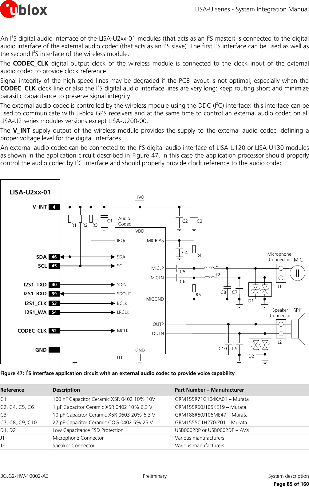
![LISA-U series - System Integration Manual 3G.G2-HW-10002-A3 Preliminary System description Page 86 of 160 Reference Description Part Number – Manufacturer L1, L2 82nH Multilayer inductor 0402 (self resonance frequency ~1 GHz) LQG15HS82NJ02 – Murata MIC 2.2 k Electret Microphone Various manufacturers R1, R2 4.7 kΩ Resistor 0402 5% 0.1 W RC0402JR-074K7L - Yageo Phycomp R3 10 kΩ Resistor 0402 5% 0.1 W RC0402JR-0710KL - Yageo Phycomp R4, R5 2.2 kΩ Resistor 0402 5% 0.1 W RC0402JR-072K2L – Yageo Phycomp SPK 32 Speaker Various manufacturers U1 16-Bit Mono Audio Voice Codec MAX9860ETG+ - Maxim Table 40: Example of components for audio voice codec application circuit If the I2S digital audio pins are not used, they can be left unconnected on the application board. Any external signal connected to the digital audio interfaces must be tri-stated when the module is in power-down mode, when the external reset is forced low and during the module power-on sequence (at least for 3 s after the start-up event), to avoid latch-up of circuits and allow a proper boot of the module. If the external signals connected to the wireless module cannot be tri-stated, insert a multi channel digital switch (e.g. Texas Instruments SN74CB3Q16244, TS5A3159, or TS5A63157) between the two-circuit connections and set to high impedance during power down mode, when external reset is forced low and during power-on sequence. 1.11.3 Voiceband processing system The voiceband processing on the LISA-U series modules is implemented in the DSP core inside the baseband chipset. The analog audio front-end of the chipset is connected to the digital system through 16 bit ADC converters in the uplink path, and through 16 bit DAC converters in the downlink path. External digital audio devices can be interfaced directly to the DSP digital processing part via the I2S digital interface. The analog amplifiers are skipped in this case. Available audio signal processing algorithms are: Speech encoding (uplink) and decoding (downlink).The following speech codecs are supported in firmware on the DSP for speech encoding and decoding: GERAN GMSK codecs GSM HR (GSM Half Rate) GSM FR (GSM Full Rate) GSM EFR (GSM Enhanced Full Rate) HR AMR (GSM Half Rate Adaptive Multi Rate - Narrow Band) FR AMR (GSM Full Rate Adaptive Multi Rate - Narrow Band) FR AMR-WB (GSM Full Rate Adaptive Multi Rate - Wide Band) UTRAN codecs: UMTS AMR2 (UMTS Adaptive Multi Rate version 2 – Narrow Band) UMTS AMR-WB (UMTS Adaptive Multi Rate – Wide Band) Mandatory sub-functions: Discontinuous transmission, DTX (GSM 46.031, 46.041, 46.081 and 46.093 standards) Voice activity detection, VAD (GSM 46.032, 46.042, 46.082 and 46.094 standards) Background noise calculation (GSM 46.012, 46.022, 46.062 and 46.092 standards) Function configurable via specific AT commands (refer to the u-blox AT Commands Manual [3]) Signal routing: +USPM command](https://usermanual.wiki/u-blox/LISAU230/User-Guide-1727756-Page-86.png)
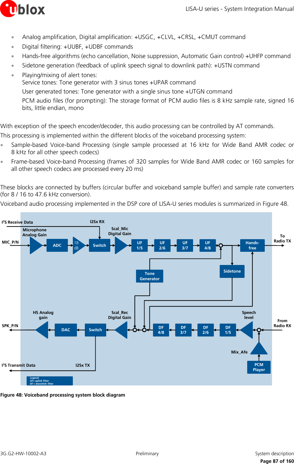
![LISA-U series - System Integration Manual 3G.G2-HW-10002-A3 Preliminary System description Page 88 of 160 1.12 General Purpose Input/Output (GPIO) LISA-U1 series modules provide 5 pins (GPIO1-GPIO5), while LISA-U2 series modules provide up to 14 pins (GPIO1-14) which can be configured as general purpose input or output, or can be configured to provide special functions via u-blox AT commands (for further details refer to u-blox AT Commands Manual [3], +UGPIOC, +UGPIOR, +UGPIOW, +UGPS, +UGPRF, +USPM). The following functions are available in the LISA-U series modules: GSM Tx burst indication: GPIO1 pin can be configured by AT+UGPIOC to indicate when a GSM Tx burst/slot occurs, setting the parameter <gpio_mode> of AT+UGPIOC command to 9. No GPIO pin is by default configured to provide the “GSM Tx burst indication” function. The pin configured to provide the “GSM Tx burst indication” function is set as o Output / High, since ~10 µs before the start of first Tx slot, until ~5 µs after the end of last Tx slot o Output / Low, otherwise The pin configured to provide the “GSM Tx burst indication” function can be connected on the application board to an input pin of an application processor to indicate when a GSM Tx burst/slot occurs. GPS supply enable: The GPIO2 is by default configured by AT+UGPIOC command to enable or disable the supply of the u-blox GPS receiver connected to the wireless module. The GPIO1, GPIO3, GPIO4 or GPIO5 pins can be configured to provide the “GPS supply enable” function, alternatively to the default GPIO2 pin, setting the parameter <gpio_mode> of AT+UGPIOC command to 3. The “GPS supply enable” mode can be provided only on one pin per time: it is not possible to simultaneously set the same mode on another pin. The pin configured to provide the “GPS supply enable” function is set as o Output / High, to switch on the u-blox GPS receiver, if the parameter <mode> of AT+UGPS command is set to 1 o Output / Low, to switch off the u-blox GPS receiver, if the parameter <mode> of AT+UGPS command is set to 0 (default setting) The pin configured to provide the “GPS supply enable” function must be connected to the active-high enable pin (or the active-low shutdown pin) of the voltage regulator that supplies the u-blox GPS receiver on the application board. LISA-U200-00 modules version don’t support “GPS supply enable” function. GPS data ready: Only the GPIO3 pin provides the “GPS data ready” function, to sense when a u-blox GPS receiver connected to the wireless module is ready to send data via the DDC (I2C) interface, setting the parameter <gpio_mode> of AT+UGPIOC command to 4. The pin configured to provide the “GPS data ready” function will be set as o Input, to sense the line status, waking up the wireless module from idle-mode when the u-blox GPS receiver is ready to send data via the DDC (I2C) interface; this is possible if the parameter <mode> of AT+UGPS command is set to 1 and the parameter <GPS_IO_configuration> of AT+UGPRF command is set to 16 o Tri-state with an internal active pull-down enabled, otherwise (default setting) The pin that provides the “GPS data ready” function must be connected to the data ready output of the u-blox GPS receiver (i.e. the pin TxD1 of the u-blox GPS receiver) on the application board.](https://usermanual.wiki/u-blox/LISAU230/User-Guide-1727756-Page-88.png)
![LISA-U series - System Integration Manual 3G.G2-HW-10002-A3 Preliminary System description Page 90 of 160 The pin configured to provide the “Network status indication” function can be connected on the application board to an input pin of an application processor or can drive a LED by a transistor with integrated resistors to indicate network status. Module status indication: The GPIO13 and GPIO1 pins can be configured to indicate module status (power-off mode, i.e. module switched off, versus idle, active or connected mode, i.e. module switched on), properly setting the parameter <gpio_mode> of AT+UGPIOC command to 10. No GPIO pin is by default configured to provide the “Module status indication”. The pin configured to provide the “Module status indication” function is set as o Output / High, when the module is switched on (any operating mode during module normal operation: idle, active or connected mode) o Output / Low, when the module is switched off (power off mode) The “Module status indication” mode can be provided only on one pin at a time: it is not possible to simultaneously set the same mode on another pin. LISA-U1 series modules and LISA-U200-00 modules versions don’t support “Module status indication”. Module operating mode indication: The GPIO14 and GPIO5 pins can be configured to indicate module operating mode (idle-mode versus active or connected mode), properly setting the parameter <gpio_mode> of AT+UGPIOC command to 11. No GPIO pin is by default configured to provide the “Module operating mode indication”. The pin configured to provide the “Module operating mode indication” function is set as o Output / High, when the module is in active or connected mode o Output / Low, when the module is in idle-mode (that can be reached if power saving is enabled by +UPSV AT command: for further details refer to u-blox AT Commands Manual [3]) The “Module operating mode indication” mode can be provided only on one pin at a time: it is not possible to simultaneously set the same mode on another pin. LISA-U1 series modules and LISA-U200-00 versions don’t support “Module operating mode indication”. I2S digital audio interface: The GPIO6, GPIO7, GPIO8, GPIO9 pins are by default configured as the second I2S digital audio interface (I2S1_RXD, I2S1_TXD, I2S1_CLK, I2S1_WA respectively). Only these pins can be configured as the second I2S digital audio interface, correctly setting the parameter <gpio_mode> of AT+UGPIOC command to 12 (default setting). LISA-U1 series modules and LISA-U200-00 versions don’t support the second I2S digital audio interface over GPIOs. SPI serial interface: GPIO10, GPIO11, GPIO12, GPIO13 and GPIO14 pins are by default configured as the SPI / IPC serial interface (SPI_SCLK, SPI_MOSI, SPI_MISO, SPI_SRDY and SPI_MRDY respectively). Only these pins can be configured as the SPI / IPC serial interface, correctly setting the parameter <gpio_mode> of AT+UGPIOC command to 13 (default setting).](https://usermanual.wiki/u-blox/LISAU230/User-Guide-1727756-Page-90.png)
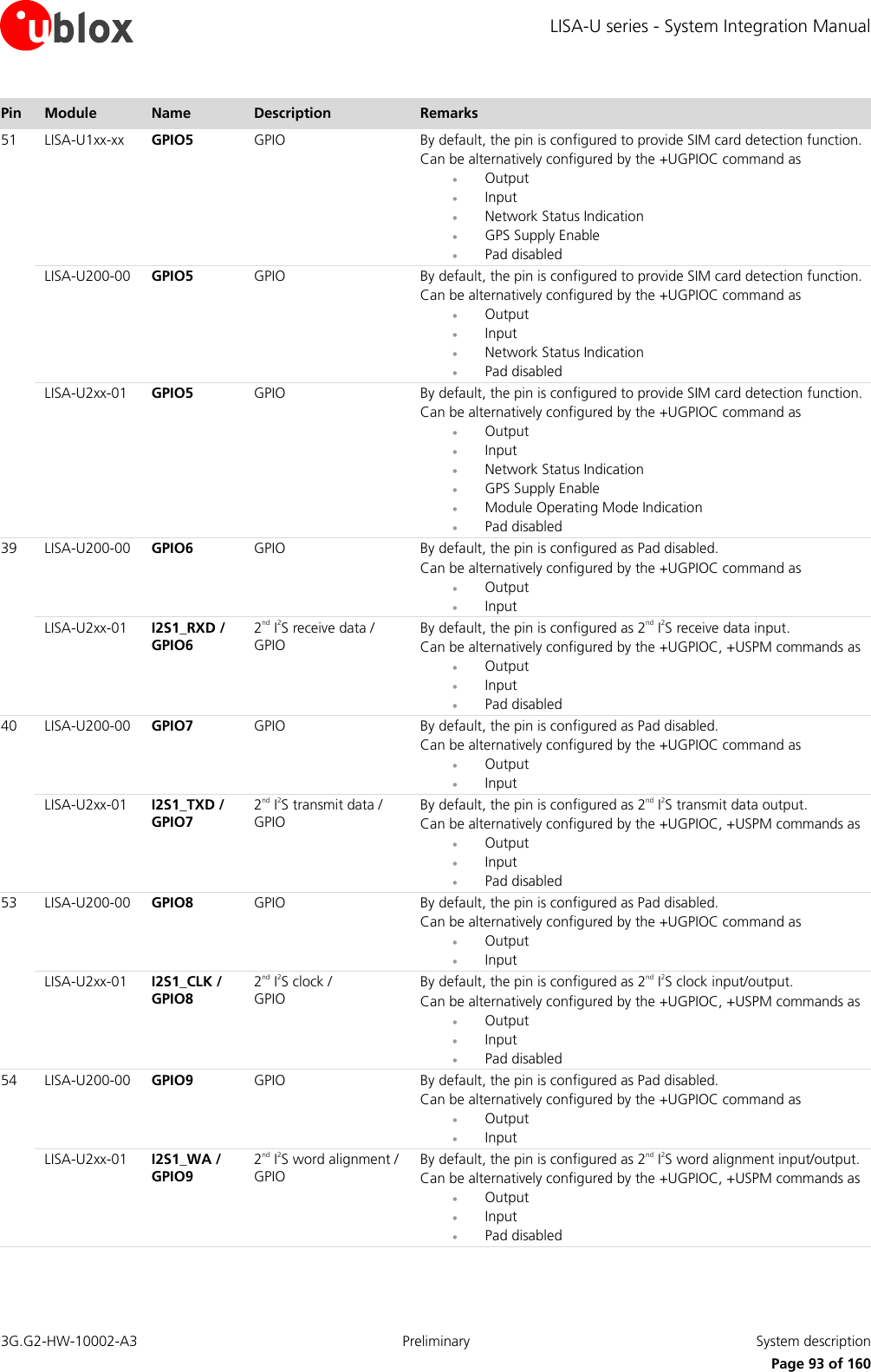
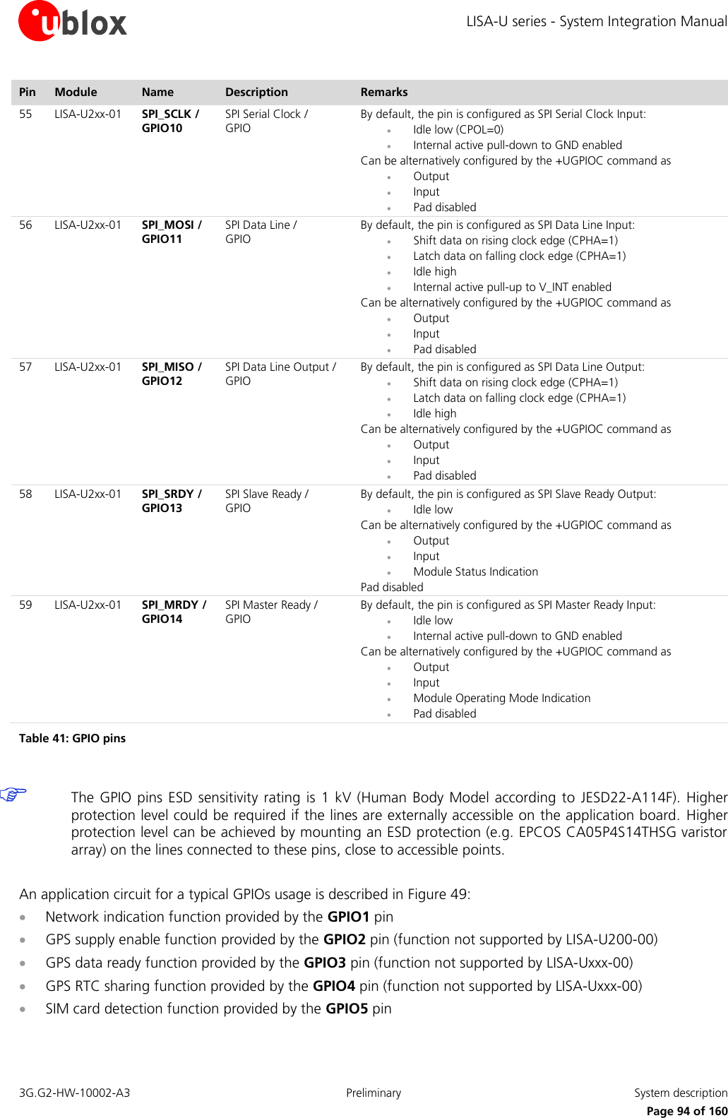
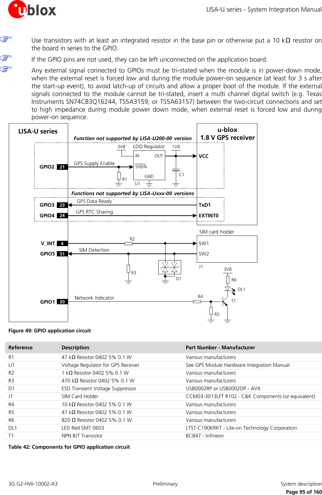
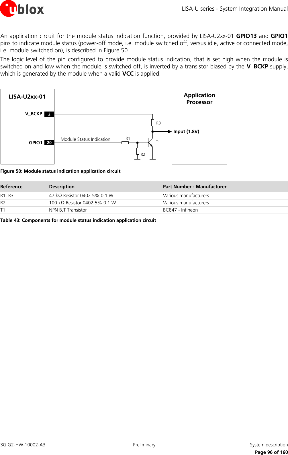
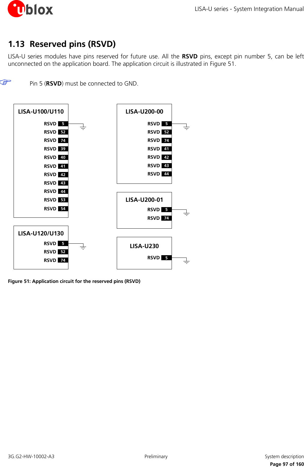
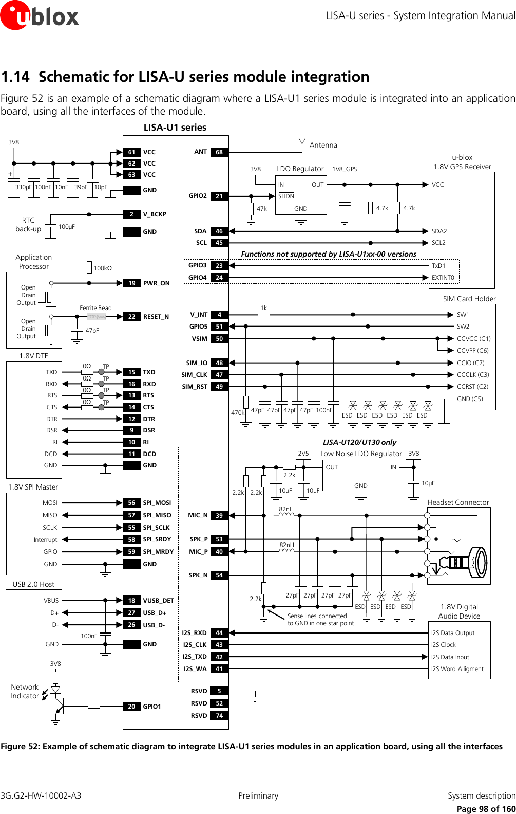
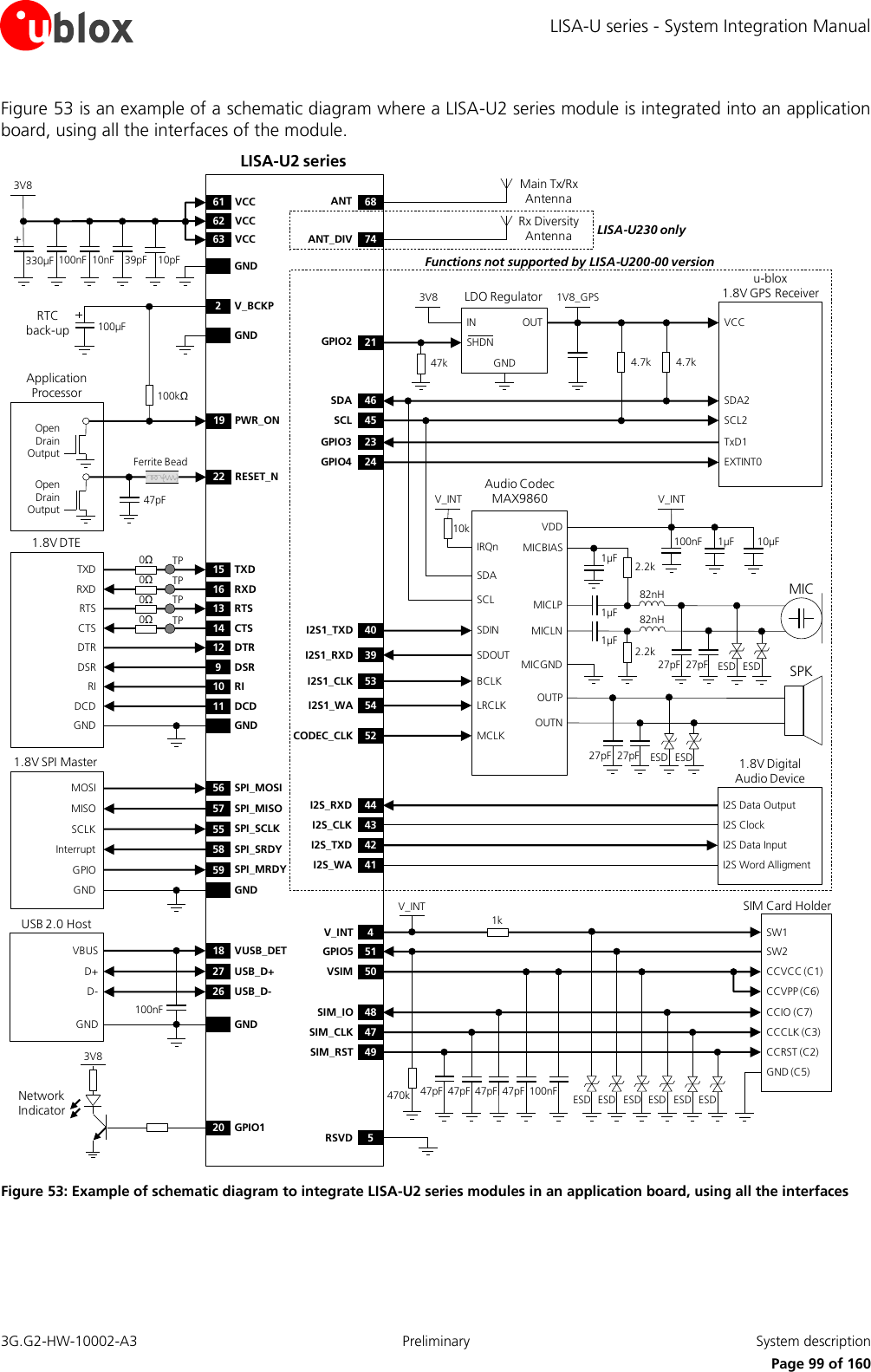
![LISA-U series - System Integration Manual 3G.G2-HW-10002-A3 Preliminary System description Page 100 of 160 1.15 Approvals LISA-U series modules have been or will be approved under the following schemes: [EU] R&TTE (Radio and Telecommunications Terminal Equipment Directive) [EU] CE (Conformité Européenne) [EU] GCF – CC (Global Certification Forum-Certification Criteria) [EU] GCF – FT (Global Certification Forum- Field Trials) [USA] FCC (Federal Communications Commission) [USA] PTCRB (PCS Type Certification Review Board) [Canada] IC (Industry Canada) [South Africa] ICASA (Independent Communications Authority of South Africa) [Australia] a-tick [Korea] KCC (Korean Communications Commission) [Japan] JATE (Japan Approvals Institute for Telecommunications Equipment) [Japan] TELEC (Telecom Engineering Center) [Taiwan] NCC (National Communications Commission) LISA-U series modules will be approved by the following network operators: [USA] AT&T [Canada] Rogers [EU][AUS] Vodafone [AUS] Telstra [EU] Tmobile [Japan] NTTDoCoMo [EU] Orange 1.15.1 R&TTED and European Conformance CE mark Products bearing the CE marking comply with the R&TTE Directive (99/5/EC), EMC Directive (89/336/EEC) and the Low Voltage Directive (73/23/EEC) issued by the Commission of the European Community. Compliance with these directives implies conformity to the following European Norms: Radio Frequency spectrum efficiency: o EN 301 511 o EN 301 908-1 o EN 301 908-2 Electromagnetic Compatibility: o EN 301 489-1 o EN 301 489-7 o EN 301 489-24 Safety o EN 60950-1: 2006 o EN62311: 2008 Notified Body identification number for LISA-U100, LISA-U110, LISA-U120 and LISA-U130 is 0890. Notified Body identification number for LISA-U200 is 0682.](https://usermanual.wiki/u-blox/LISAU230/User-Guide-1727756-Page-100.png)
![LISA-U series - System Integration Manual 3G.G2-HW-10002-A3 Preliminary Design-In Page 104 of 160 2 Design-In 2.1 Design-in checklist This section provides a design-in checklist. 2.1.1 Schematic checklist The following are the most important points for a simple schematic check: DC supply must provide a nominal voltage at VCC pin above the minimum operating range limit. DC supply must be capable of providing 2.5 A current pulses, providing a voltage at VCC pin above the minimum operating range limit and with a maximum 400 mV voltage drop from the nominal value. VCC supply should be clean, with very low ripple/noise: suggested passive filtering parts can be inserted. VCC voltage must ramp from 2.5 V to 3.2 V within 1 ms to allow a proper switch-on of the module. Connect only one DC supply to VCC: different DC supply systems are mutually exclusive. Do not leave PWR_ON floating: add a pull-up resistor to V_BCKP. Don’t apply loads which might exceed the limit for maximum available current from V_INT supply. Check that voltage level of any connected pin does not exceed the relative operating range. Capacitance and series resistance must be limited on each SIM signal to match the SIM specifications. Insert the suggested low capacitance ESD protection and passive filtering parts on each SIM signal. Check UART signals direction, since the signal names follow the ITU-T V.24 Recommendation [4]. Provide appropriate access to USB interface and/or to UART RxD, TxD lines and access to PWR_ON and/or RESET_N lines on the application board in order to flash/upgrade the module firmware. Provide appropriate access to USB interface and/or to UART RxD, TxD, CTS, RTS lines for debugging. Capacitance and series resistance must be limited on each line of the SPI / IPC interface. Add a proper pull-up resistor to a proper supply on each DDC (I2C) interface line, if the interface is used. Capacitance and series resistance must be limited on each line of the DDC interface. Use transistors with at least an integrated resistor in the base pin or otherwise put a 10 kΩ resistor on the board in series to the GPIO when those are used to drive LEDs. Connect the pin number 5 (RSVD) to ground. Insert the suggested passive filtering parts on each used analog audio line. Check the digital audio interface specifications to connect a proper device. Capacitance and series resistance must be limited on CODEC_CLK line and each I2S interface line. Provide proper precautions for ESD immunity as required on the application board. Any external signal connected to the UART interface, SPI/IPC interface, I2S interfaces and GPIOs must be tri-stated when the module is in power-down mode, when the external reset is forced low and during the module power-on sequence (at least for 3 s after the start-up event), to avoid latch-up of circuits and let a proper boot of the module. All unused pins can be left floating on the application board except the PWR_ON pin (must be connected to V_BCKP by a pull-up resistor) and the RSVD pin number 5 (must be connected to GND).](https://usermanual.wiki/u-blox/LISAU230/User-Guide-1727756-Page-104.png)
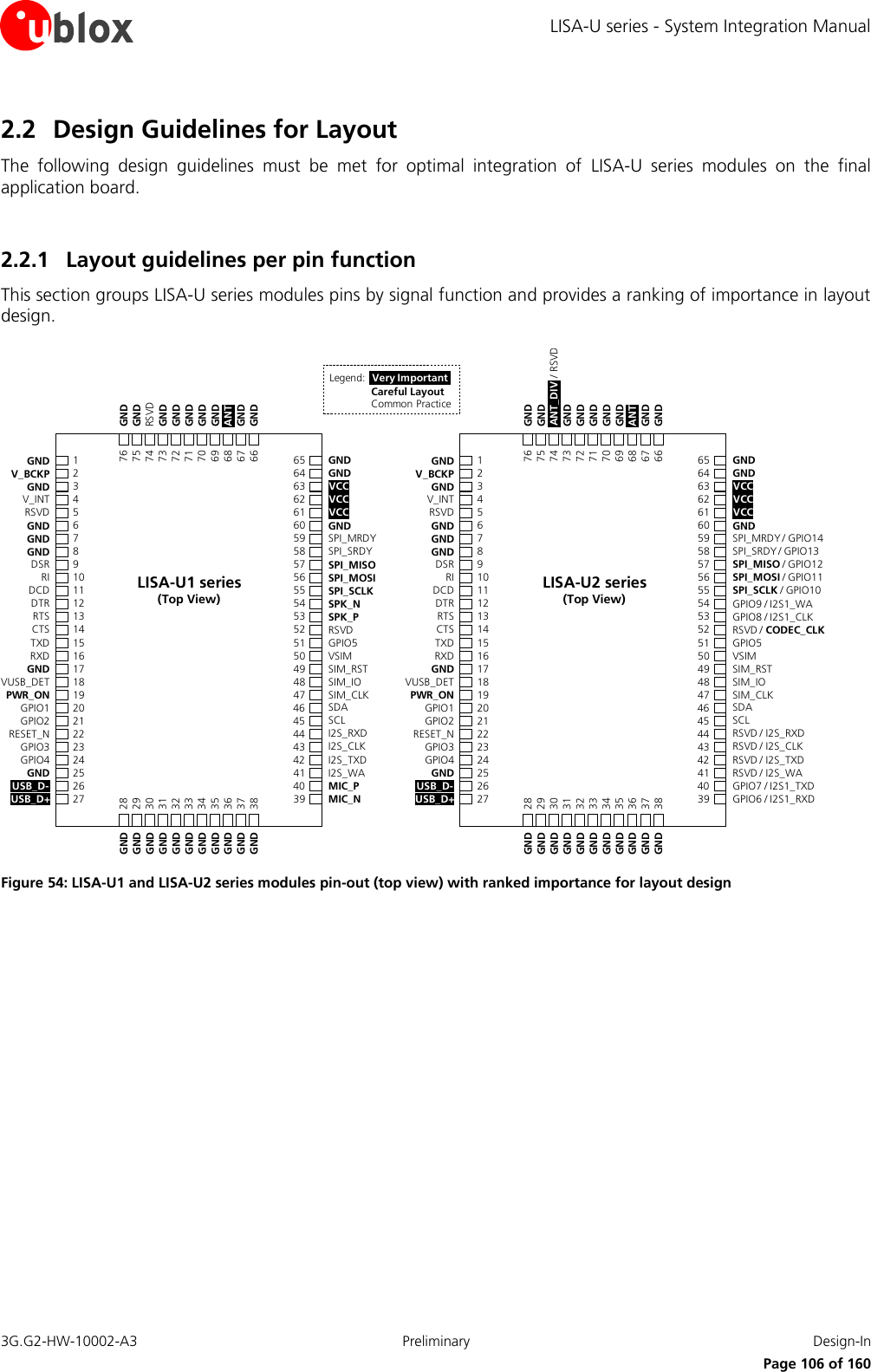
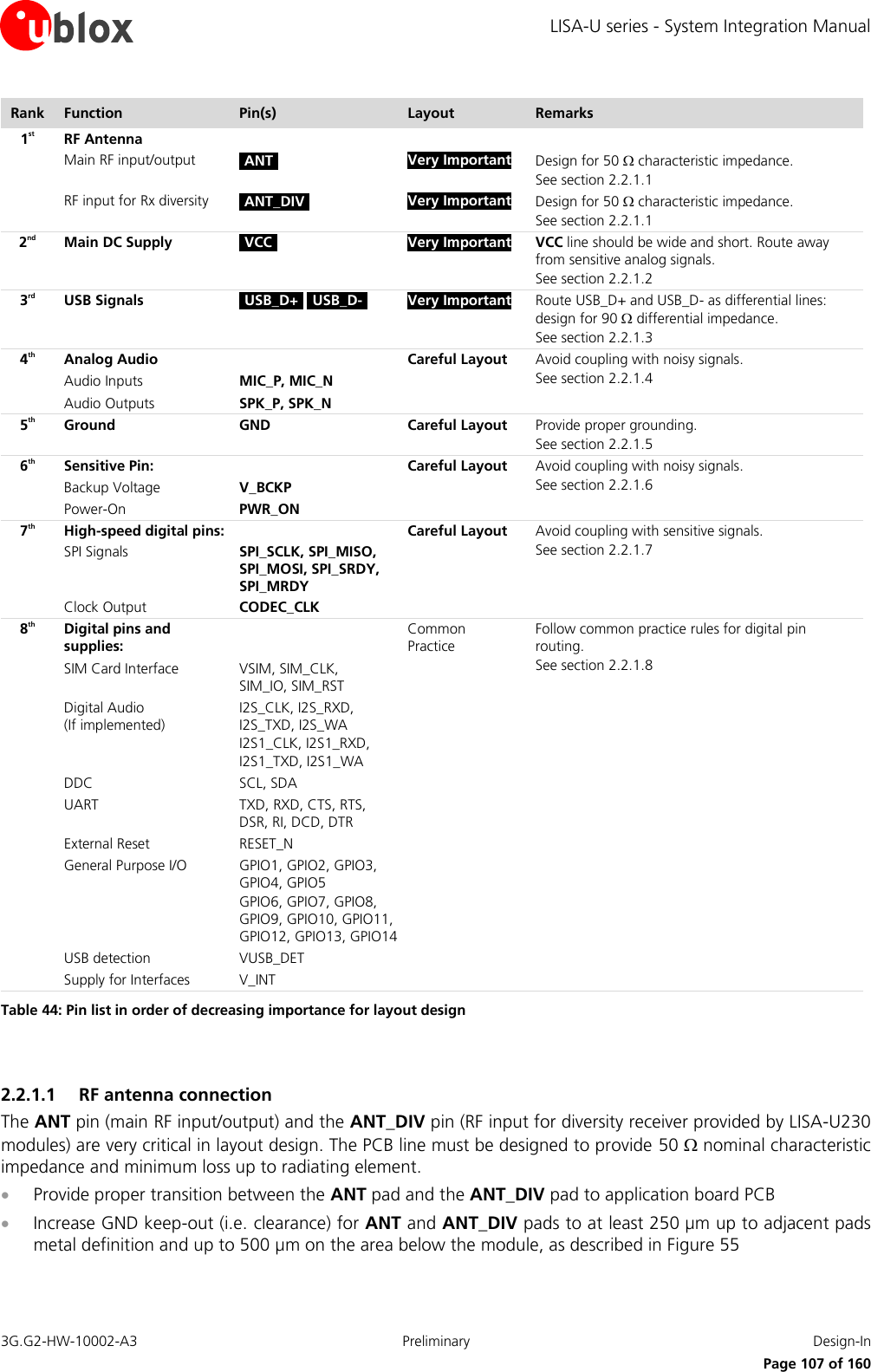
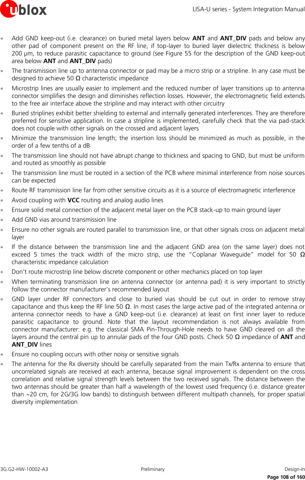
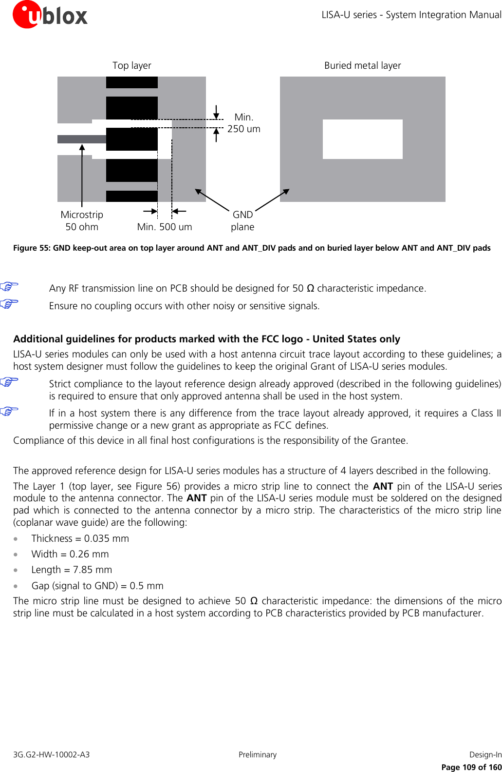
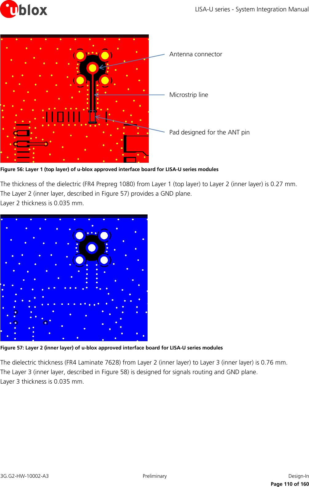
![LISA-U series - System Integration Manual 3G.G2-HW-10002-A3 Preliminary Design-In Page 116 of 160 2.2.2 Footprint and paste mask The following figure describes the footprint and provides recommendations for the paste mask for LISA-U series modules. These are recommendations only and not specifications. Note that the copper and solder masks have the same size and position. 33.2 mm [1307.1 mil] 22.4 mm [881.9 mil]2.3 mm [90.6 mil]0.8 mm [31.5 mil]1.1 mm [43.3 mil]0.8 mm [31.5 mil]1.0 mm [39.3 mil]5.7 mm [224.4 mil]33.2 mm [1307.1 mil] 22.4 mm [881.9 mil]2.3 mm [90.6 mil]1.2 mm [47.2 mil]1.1 mm [43.3 mil]0.8 mm [31.5 mil]0.9 mm [35.4 mil]5.7 mm [224.4 mil]0.6 mm [23.6 mil]Stencil: 150 µm Figure 60: LISA-U series modules suggested footprint and paste mask To improve the wetting of the half vias, reduce the amount of solder paste under the module and increase the volume outside of the module by defining the dimensions of the paste mask to form a T-shape (or equivalent) extending beyond the copper mask. The solder paste should have a total thickness of 150 µm. The paste mask outline needs to be considered when defining the minimal distance to the next component. The exact geometry, distances, stencil thicknesses and solder paste volumes must be adapted to the specific production processes (e.g. soldering etc.) of the customer. The bottom layer of LISA-U1 series modules has one unprotected copper area for GND, shown in Figure 61. The bottom layer of LISA-U2 series modules has two unprotected copper areas for GND, shown in Figure 62. Consider “No-routing” areas for the LISA-U series modules footprint as follows: signal keep-out area on the top layer of the application board, below LISA-U series modules, due to GND opening on module bottom layer (see Figure 61 and Figure 62).](https://usermanual.wiki/u-blox/LISAU230/User-Guide-1727756-Page-116.png)
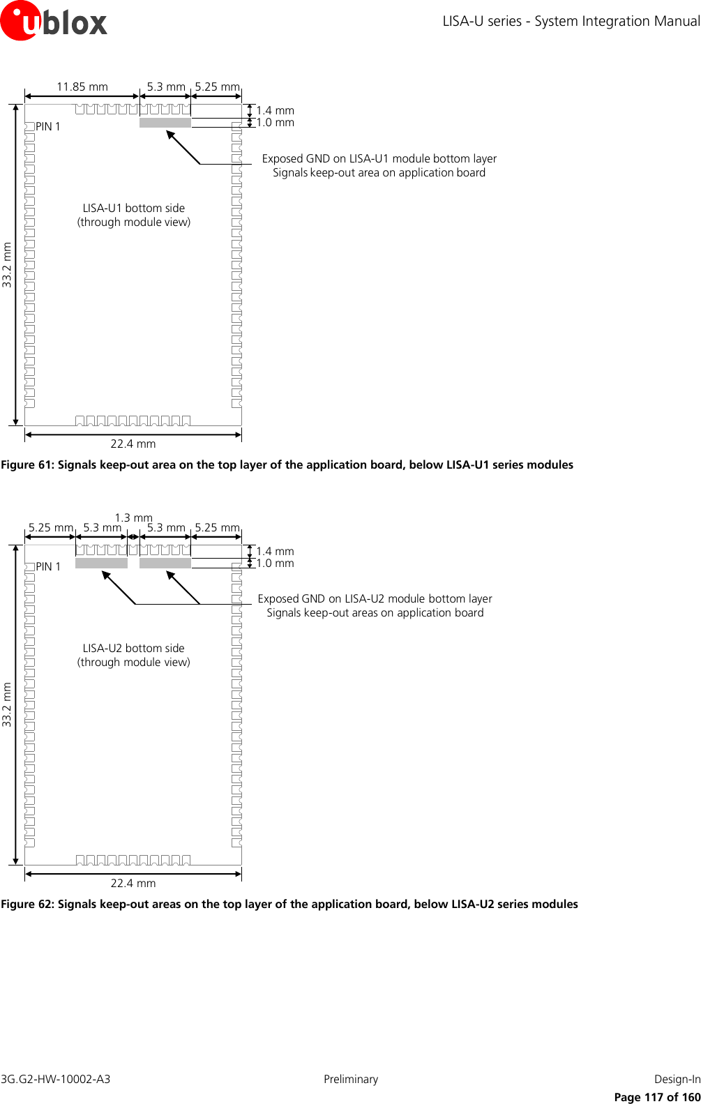
![LISA-U series - System Integration Manual 3G.G2-HW-10002-A3 Preliminary Design-In Page 118 of 160 2.2.3 Placement Optimize placement for minimum length of RF line and closer path from DC source for VCC. Make sure that RF and analog circuits are clearly separated from any other digital circuits on the system board. Provide enough clearance between the module and any external part due to solder and paste masks design. Milled edges that are present at module PCB corners, away from module pins metallization, can slightly increase module dimensions from the width and the height described in the mechanical specifications sections of LISA-U1 series Data Sheet [1] and LISA-U2 series Data Sheet [2]: provide enough clearance between module PCB corners and any other external part mounted on the application board. The heat dissipation during continuous transmission at maximum power can significantly raise the temperature of the application base-board below the LISA-U series modules: avoid placing temperature sensitive devices (e.g. GPS receiver) close to the module.](https://usermanual.wiki/u-blox/LISAU230/User-Guide-1727756-Page-118.png)
![LISA-U series - System Integration Manual 3G.G2-HW-10002-A3 Preliminary Design-In Page 119 of 160 2.3 Thermal aspects The operating temperature range is specified in LISA-U1 series Data Sheet [1] and LISA-U2 series Data Sheet [2]. The most critical condition concerning thermal performance is the uplink transmission at maximum power (data upload or voice call in connected mode), when the baseband processor runs at full speed, radio circuits are all active and the RF power amplifier is driven to higher output RF power. This scenario is not often encountered in real networks; however the application should be correctly designed to cope with it. During transmission at maximum RF power the LISA-U series modules generate thermal power that can exceed 2 W: this is an indicative value since the exact generated power strictly depends on operating condition such as the number of allocated TX slot and modulation (GMSK or 8PSK) or data rate (WCDMA), transmitting frequency band, etc. The generated thermal power must be adequately dissipated through the thermal and mechanical design of the application. The Module-to-Ambient thermal resistance (Rth,M-A) of LISA-U series modules mounted on a 90 mm x 70 mm x 1.46 mm 4-Layers PCB with a high coverage of copper in still air conditions ranges between 9 and 12 °C/W. The spreading of Rth,M-A depends on the operating condition (e.g. 2G or 3G mode, transmit band): the overall temperature distribution is influenced by the configuration of the active components during the specific mode of operation and their different thermal resistance toward the case interface. With this setup, the increase of the module temperature5 referred to idle state initial condition6 is: around 7°C during a voice call at maximum power 19°C during GPRS data transfer with 4 TX slots 16°C during EDGE data transfer with 4 TX slots up to 25°C in UMTS connection at max TX power Case-to-Ambient thermal resistance value will be different for other mechanical deployments of the module, e.g. PCB with different size and characteristics, mechanical shells enclosure, or forced air flow. The increase of thermal dissipation, i.e. reducing the thermal resistance, will decrease the operating temperature for internal circuitry of LISA-U series modules for a given operating ambient temperature. This improves the device long-term reliability for applications operating at high ambient temperature. A few techniques may be used to reduce the thermal resistance in the application: Forced ventilation air-flow within mechanical enclosure Heat sink attached to the module top side, with electrically insulated / high thermal conductivity adhesive, or on the backside of the application board, below the wireless module Connect each GND pin with solid ground layer of the application board and connect each ground area of the multilayer application board with complete via stack down to main ground layer For example, after the installation of a robust aluminum heat-sink with forced air ventilation on the back of the same application board described above, the Module-to-Ambient thermal resistance is reduced to 1.5 ÷ 3.5 °C/W. The effect of lower Rth,M-A can be seen from the module temperature which now becomes: around 1.5°C above the ambient temperature during a voice call at maximum power 3°C during GPRS data transfer with 4 TX slots 2.5°C during EDGE data transfer with 4 TX slots 5.5°C in UMTS connection at max TX power 5 Temperature is measured by internal sensor of wireless module 6 Steady state thermal equilibrium is assumed. The module’s temperature in idle state can be considered equal to ambient temperature](https://usermanual.wiki/u-blox/LISAU230/User-Guide-1727756-Page-119.png)
![LISA-U series - System Integration Manual 3G.G2-HW-10002-A3 Preliminary Design-In Page 120 of 160 2.4 Antenna guidelines Antenna characteristics are essential for good functionality of the module. Antenna radiating performance has direct impact on the reliability of connections over the Air Interface. A bad termination of the ANT pin (main RF input/output) and the ANT_DIV pin (RF input for diversity receiver provided by LISA-U230 modules) can result in poor performance of the module. The following parameters should be checked: Item Recommendations Impedance 50 Ω nominal characteristic impedance Frequency Range Depends on the LISA-U series module HW version and on the Mobile Network used. LISA-U100, LISA-U120: 824..960 MHz (GSM 850, GSM 900, UMTS B5) 1710..1990 MHz (GSM 1800, GSM 1900, UMTS B2) LISA-U110, LISA-U130: 824..960 MHz (GSM 850, GSM 900, UMTS B8) 1710..2170 MHz (GSM 1800, GSM 1900, UMTS B1) LISA-U200-00: 824..960 MHz (GSM 850, GSM 900, UMTS B5, UMTS B6) 1710..2170 MHz (GSM 1800, GSM 1900, UMTS B1, UMTS B2) LISA-U200-01, LISA-U230-01: 824..960 MHz (GSM 850, GSM 900, UMTS B5, UMTS B6, UMTS B8) 1710..2170 MHz (GSM 1800, GSM 1900, UMTS B1, UMTS B2, UMTS B4) Input Power >2 W peak V.S.W.R <2:1 recommended, <3:1 acceptable Return Loss S11<-10 dB recommended, S11<-6 dB acceptable Table 45: General recommendation for GSM antenna The antenna gain shall remain below the levels reported in the chapter 1.15.3.2 to preserve the original u-blox FCC ID. Please note that some 2G and 3G bands are overlapping. This depends on worldwide band allocation for telephony services, where different bands are deployed for different geographical regions. If the LISA-U110, LISA-U130 or LISA-U2 series modules are planned for use on the entire supported bands, then an antenna that supports the 824..960 MHz and the 1710..2170 MHz frequency range should be selected. If the LISA-U100 or LISA-U120 modules are planned for use with the entire range of supported bands, then an antenna that supports the 824..960 MHz and the 1710..1990 MHz frequency range should be selected. Otherwise, for fixed applications in specific geographical region, antenna requirements can be relaxed for non-deployed frequency bands. Refer to the operating RF frequency bands table in LISA-U1 series Data Sheet [1] and LISA-U2 series Data Sheet [2] for the detailed uplink and downlink frequency ranges of each supported band. LISA-U230 modules provide 2G and 3G dynamic receive diversity (Rx diversity) capability to improve the quality and reliability of the wireless link. This feature can be optionally used connecting a second antenna to the ANT_DIV pin, to receive an RF input signal that is processed by the module to increase the performance. All the antenna guidelines and recommendations reported are applicable also to the Rx diversity antenna design, even if the antenna for the Rx diversity is not used to transmit. GSM antennas are typically available as: Linear monopole: typical for fixed applications. The antenna extends mostly as a linear element with a dimension comparable to lambda/4 of the lowest frequency of the operating band. Magnetic base may be available. Cable or direct RF connectors are common options. The integration normally requires the fulfillment of some minimum guidelines suggested by antenna manufacturer Patch-like antenna: better suited for integration in compact designs (e.g. mobile phone). These are mostly custom designs where the exact definition of the PCB and product mechanical design is fundamental for tuning of antenna characteristics](https://usermanual.wiki/u-blox/LISAU230/User-Guide-1727756-Page-120.png)
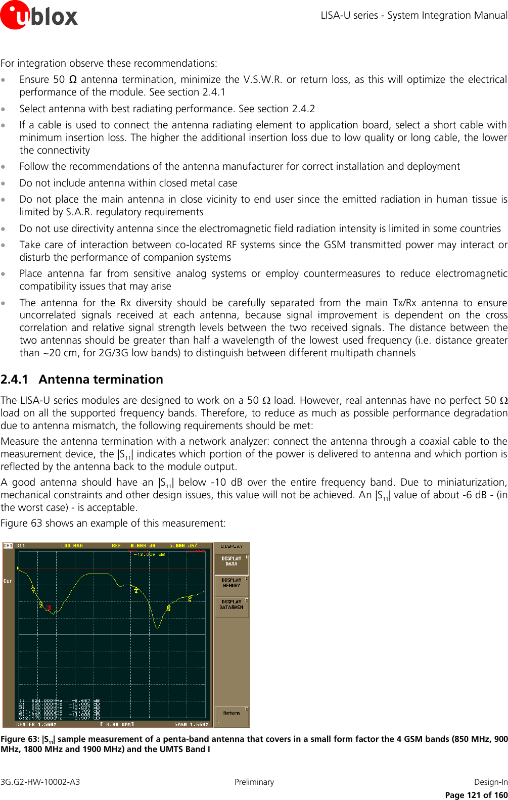
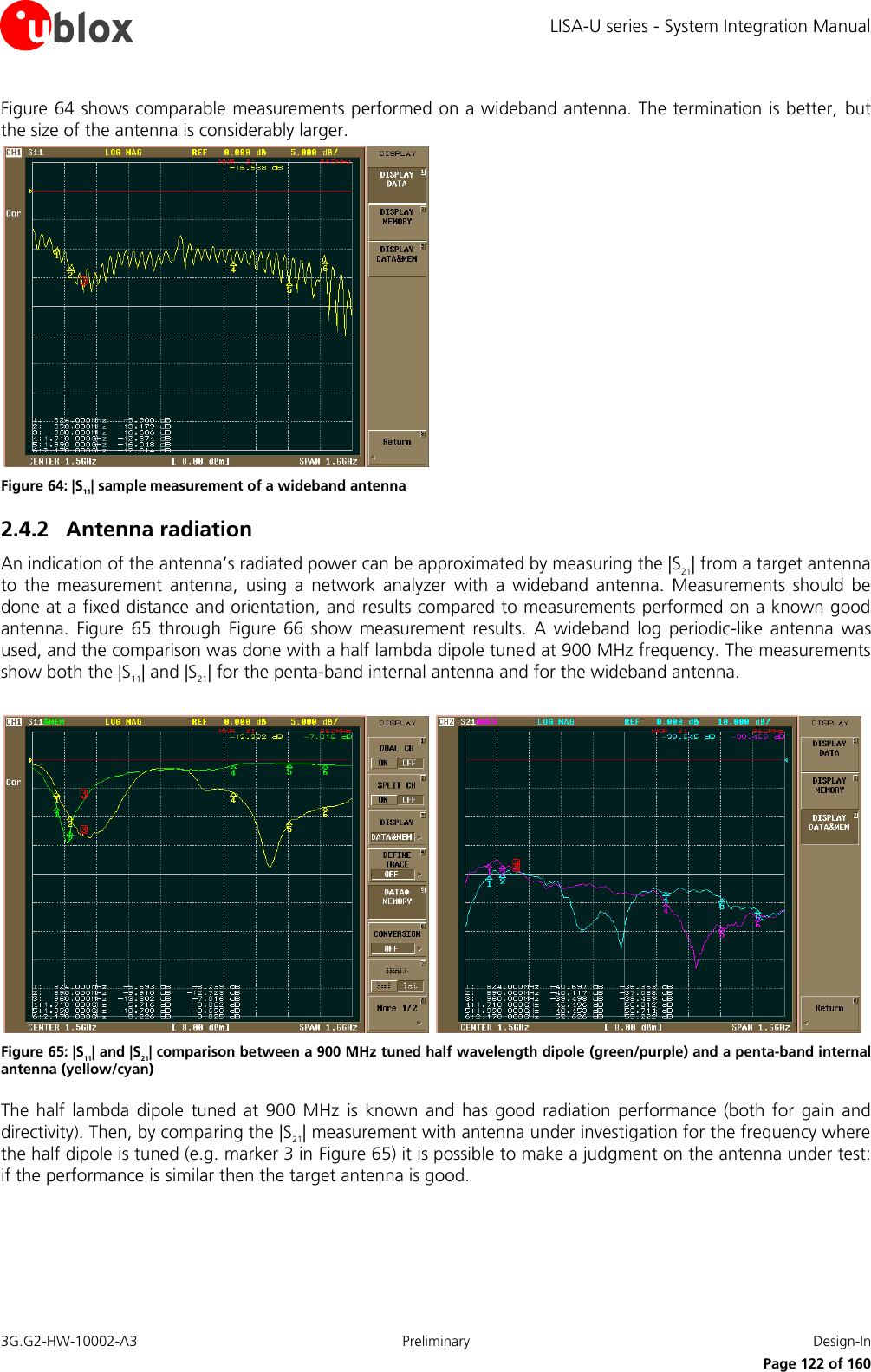
![LISA-U series - System Integration Manual 3G.G2-HW-10002-A3 Preliminary Design-In Page 123 of 160 Figure 66: |S11| and |S21| comparison between a 900 MHz tuned half wavelength dipole (green/purple) and a wideband commercial antenna (yellow/cyan) Instead if |S21| values for the tuned dipole are much better than the antenna under evaluation (like for marker 1/2 area of Figure 66, where dipole is 5 dB better), then it can be argued that the radiation of the target antenna (the wideband dipole in this case) is considerably less. The same procedure should be repeated on other bands with half wavelength dipole re-tuned to the band under investigation. For good antenna radiation performance, antenna dimensions should be comparable to a quarter of the wavelength. Different antenna types can be used for the module, many of them (e.g. patch antennas, monopole) are based on a resonating element that works in combination with a ground plane. The ground plane, ideally infinite, can be reduced down to a minimum size that must be similar to one quarter of the wavelength of the minimum frequency that has to be radiated (transmitted/received). Numerical sample: frequency = 1 GHz wavelength = 30 cm minimum ground plane (or antenna size) = 7.5 cm. Below this size, the antenna efficiency is reduced. 2.4.3 Antenna detection functionality The internal antenna detect circuit is based on ADC measurement at ANT: the RF port is DC coupled to the ADC unit in the baseband chip which injects a DC current (10 µA for 128 µs) on ANT and measures the resulting DC voltage to evaluate the resistance from ANT pad to GND. The antenna detection is forced by the +UANTR AT command: refer to the u-blox AT Commands Manual [3] for more details on how to access this feature. To achieve antenna detection functionality, use an RF antenna with built-in resistor from ANT signal to GND, or implement an equivalent solution with a circuit between the antenna cable connection and the radiating element as shown in Figure 67.](https://usermanual.wiki/u-blox/LISAU230/User-Guide-1727756-Page-123.png)
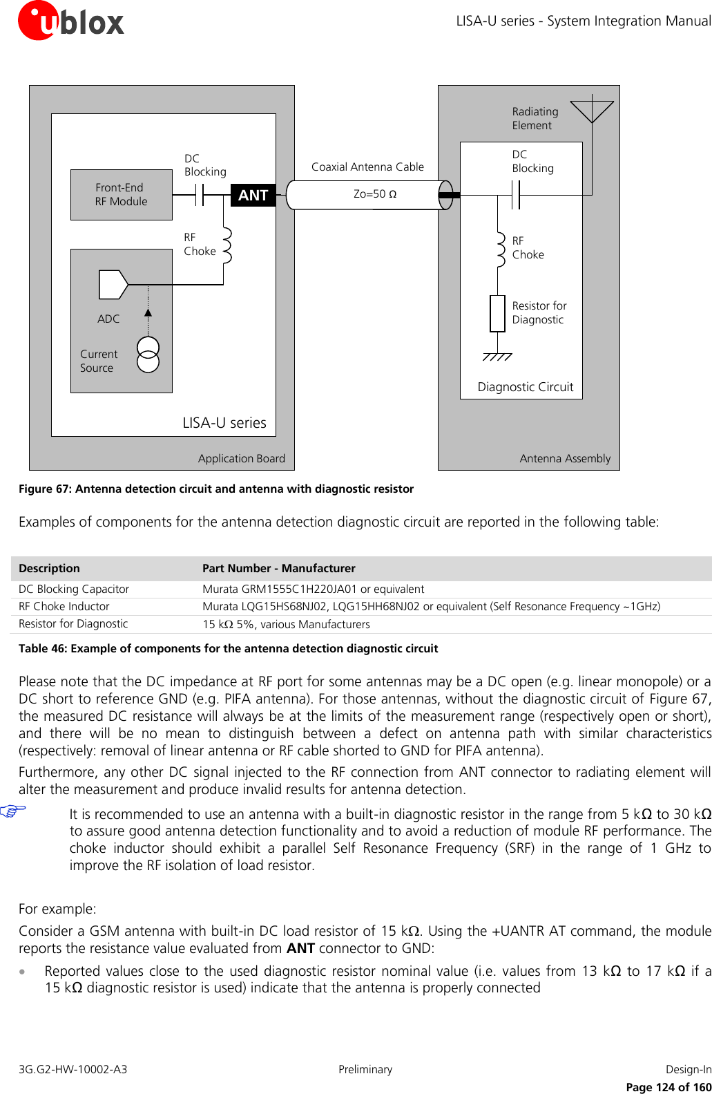
![LISA-U series - System Integration Manual 3G.G2-HW-10002-A3 Preliminary Design-In Page 125 of 160 Values close to the measurement range maximum limit (approximately 50 kΩ) or an open-circuit “over range” report (see u-blox AT Commands Manual [3]) means that that the antenna is not connected or the RF cable is broken Reported values below the measurement range minimum limit (1 kΩ) will highlight a short to GND at antenna or along the RF cable Measurement inside the valid measurement range and outside the expected range may indicate an improper connection, damaged antenna or wrong value of antenna load resistor for diagnostic Reported value could differ from the real resistance value of the diagnostic resistor mounted inside the antenna assembly due to antenna cable length, antenna cable capacity and the used measurement method](https://usermanual.wiki/u-blox/LISAU230/User-Guide-1727756-Page-125.png)
![LISA-U series - System Integration Manual 3G.G2-HW-10002-A3 Preliminary Design-In Page 126 of 160 2.5 ESD precautions 2.5.1 ESD immunity test overview The immunity of the device (i.e. the application board where LISA-U series module is mounted) to the Electrostatic Discharge (ESD) must be certified in compliance to the testing standard CENELEC EN 61000-4-2 [10] and the radio equipment standards ETSI EN 301 489-1 [11], ETSI EN 301 489-7 [12], ETSI EN 301 489-24 [13], which requirements are summarized in Table 47. The ESD immunity test is performed at the enclosure port, defined by ETSI EN 301 489-1 [11] as the physical boundary through which the electromagnetic field radiates. If the device implements an integral antenna, the enclosure port is seen as all insulating and conductive surfaces housing the device. If the device implements a removable antenna, the antenna port can be separated from the enclosure port. The antenna port includes the antenna element and its interconnecting cable surfaces. The applicability of ESD immunity test to the whole device depends on the device classification as defined by ETSI EN 301 489-1 [11]. Applicability of ESD immunity test to the relative device ports or the relative interconnecting cables to auxiliary equipments, depends on device accessible interfaces and manufacturer requirements, as defined by ETSI EN 301 489-1 [11]. Contact discharges are performed at conductive surfaces, while air discharges are performed at insulating surfaces. Indirect contact discharges are performed on the measurement setup horizontal and vertical coupling planes as defined in CENELEC EN 61000-4-2 [10]. For the definition of integral antenna, removable antenna, antenna port, device classification refer to ETSI EN 301 489-1 [11]. The contact and air discharges are defined in CENELEC EN 61000-4-2 [10]. Application Category Immunity Level All exposed surfaces of the radio equipment and ancillary equipment in a representative configuration Contact Discharge 4 kV Air Discharge 8 kV Table 47: Electromagnetic Compatibility ESD immunity requirements as defined by standards CENELEC EN 61000-4-2, ETSI EN 301 489-1 V1.8.1, ETSI EN 301 489-7 V1.3.1, ETSI EN 301 489-24 V1.4.1 2.5.2 ESD immunity test of LISA-U series reference design Although electromagnetic compatibility (EMC) certification must be performed by the final application of the radio equipment under test (i.e. the application board where LISA-U series module is mounted), EMC certification (including ESD immunity) have been successfully performed on LISA-U1 series and LISA-U200-00 modules reference design according to CENELEC EN 61000-4-2 [10], ETSI EN 301 489-1 [11], ETSI EN 301 489-7 [12] and ETSI EN 301 489-24 [13] standards. The EMC approved reference design consists of a LISA-U1 series or a LISA-U200-00 module soldered on a motherboard which provides an interface to power supply, SIM card, headset and communication port. An external antenna is connected to an SMA connector provided on the motherboard. Since an external antenna is used, the antenna port can be separated from the enclosure port. The reference design is not enclosed in a box so the enclosure port is not indentified with physical surfaces. Therefore, some test cases cannot be applied. Only the antenna port is identified as accessible for direct ESD exposure. The reference application implements all precautions described in the section 2.5.3. ESD immunity test results and applicability are reported in Table 48 according to test requirements CENELEC EN 61000-4-2 [10], ETSI EN 301 489-1 [11], ETSI EN 301 489-7 [12] and ETSI EN 301 489-24 [13].](https://usermanual.wiki/u-blox/LISAU230/User-Guide-1727756-Page-126.png)
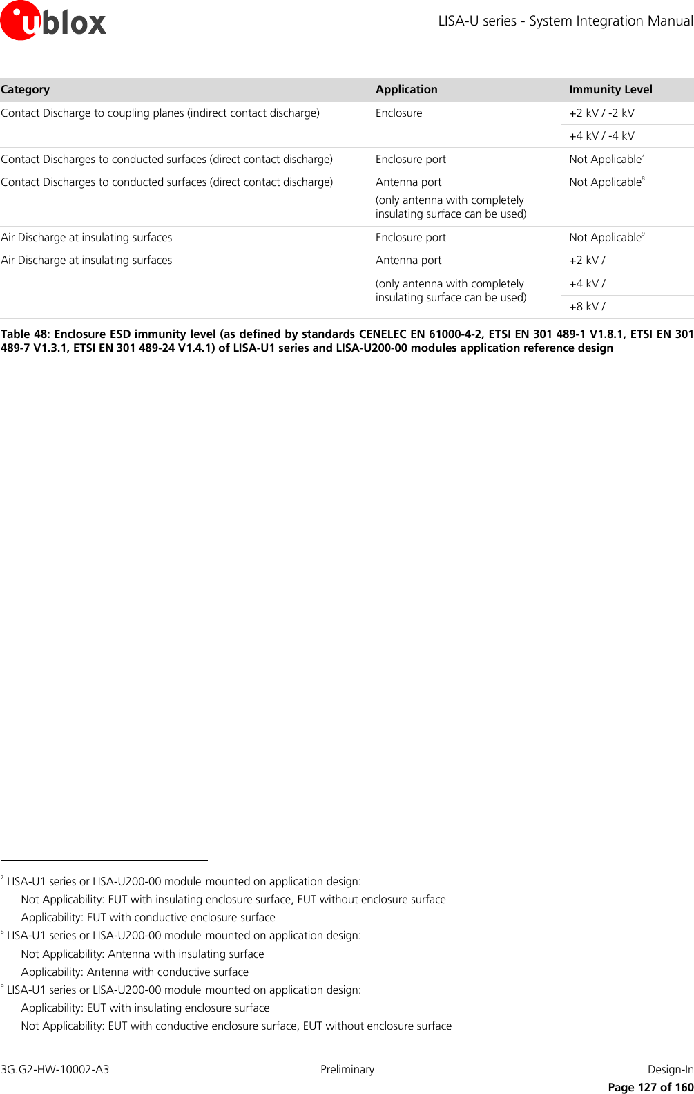
![LISA-U series - System Integration Manual 3G.G2-HW-10002-A3 Preliminary Design-In Page 128 of 160 2.5.3 ESD application circuits The application circuits described in this section should be implemented, depending on the application board handling, to satisfy ESD immunity test requirements. These are defined in CENELEC EN 61000-4-2 [10], ETSI EN 301 489-1 [11] and ETSI EN 301 489-7 [12], and performed at the device enclosure in compliance to the category level defined in ETSI EN 301 489-1 [11]. The test requirements are summarized in Table 47. Antenna interface With LISA-U1 series modules, the ANT pin provides ESD immunity up to 500 V (contact and air discharge according to IEC 61000-4-2): higher protection level is required if the line is externally accessible on the device (i.e. the application board where LISA-U1 series module is mounted). The following precautions are suggested to satisfy ESD immunity test requirements using LISA-U1 series modules: If the device implements an embedded antenna, the insulating enclosure of the device should provide protection to direct contact discharge up to +4 kV / -4 kV and protection to air discharge up to +8 kV / -8 kV to the antenna interface If the device implements an external antenna, the antenna and its connecting cable should provide a completely insulated enclosure able to provide protection to direct contact discharge up to +4 kV / -4 kV and protection to air discharge up to +8 kV / -8 kV to the whole antenna and cable surfaces With the LISA-U200-00 module, the ANT pin provides ESD immunity up to 1000 V (contact and air discharge according to IEC 61000-4-2): higher protection level is required if the line is externally accessible on the device (i.e. the application board where LISA-U200-00 module is mounted). The following precautions are suggested for satisfying ESD immunity test requirements using LISA-U200-00 modules: If the device implements an embedded antenna, the device insulating enclosure should provide protection to direct contact discharge up to +4 kV / -4 kV and protection to air discharge up to +8 kV / -8 kV to the antenna interface If the device implements an external antenna, the antenna and its connecting cable should provide a completely insulated enclosure able to provide protection to direct contact discharge up to +4 kV / -4 kV and protection to air discharge up to +8 kV / -8 kV to the whole antenna and cable surfaces If the device implements an external antenna and the antenna and its connecting cable don’t provide a completely insulated enclosure able to provide protection to direct contact discharge up to +4 kV / -4 kV and protection to air discharge up to +8 kV / -8 kV to the whole antenna and cable surfaces, an external high pass filter, consisting of a series 15 pF capacitor (Murata GRM1555C1H150JA01) and a shunt 39 nH coil (Murata LQG15HN39NJ102) should be implemented at the antenna port as described in Figure 68 Antenna detection functionality is not provided when implementing the high pass filter described in Figure 68 and Table 49, as ESD protection for the LISA-U200-00 antenna port.](https://usermanual.wiki/u-blox/LISAU230/User-Guide-1727756-Page-128.png)
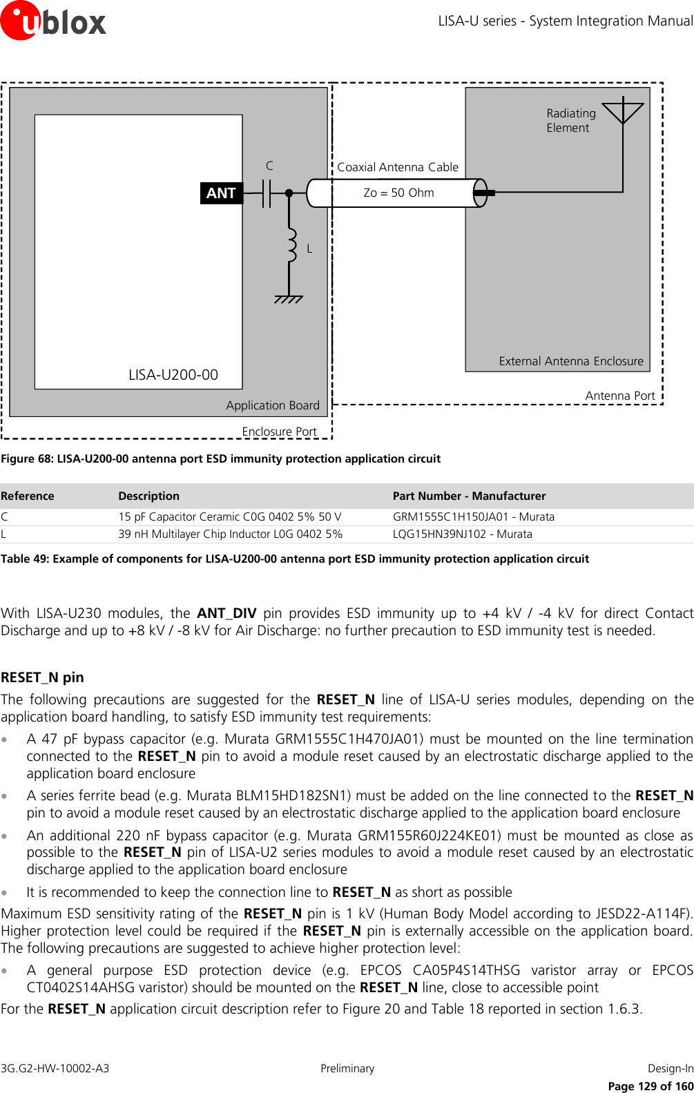
![LISA-U series - System Integration Manual 3G.G2-HW-10002-A3 Preliminary Design-In Page 130 of 160 SIM interface The following precautions are suggested for LISA-U series modules SIM interface (VSIM, SIM_RST, SIM_IO, SIM_CLK pins), depending on the application board handling, to satisfy ESD immunity test requirements: A 47 pF bypass capacitor (e.g. Murata GRM1555C1H470J) must be mounted on the lines connected to VSIM, SIM_RST, SIM_IO and SIM_CLK pins to assure SIM interface functionality when an electrostatic discharge is applied to the application board enclosure It is suggested to use as short as possible connection lines at SIM pins Maximum ESD sensitivity rating of SIM interface pins is 1 kV (Human Body Model according to JESD22-A114F). Higher protection level could be required if SIM interface pins are externally accessible on the application board. The following precautions are suggested to achieve higher protection level: A low capacitance (i.e. less than 10 pF) ESD protection device (e.g. Infineon ESD8V0L2B-03L or AVX USB0002) should be mounted on each SIM interface line, close to accessible points (i.e. close to the SIM card holder) For the SIM interface application circuit description refer to Figure 21 and Table 21 reported in section 1.8. Other pins and interfaces All the module pins that are externally accessible on the device (i.e. the application board where LISA-U series module is mounted) should be included in the ESD immunity test since they are considered to be a port as defined in ETSI EN 301 489-1 [11]. Depending on applicability, to satisfy ESD immunity test requirements according to ESD category level, all the module pins that are externally accessible should be protected up to +4 kV / -4 kV for direct Contact Discharge and up to +8 kV / -8 kV for Air Discharge applied to the enclosure surface. The maximum ESD sensitivity rating of all the other pins of the module is 1 kV (Human Body Model according to JESD22-A114F). Higher protection level could be required if the relative pin is externally accessible on the application board. The following precautions are suggested to achieve higher protection level: USB interface: a very low capacitance (i.e. less or equal to 1 pF) ESD protection device (e.g. Tyco Electronics PESD0402-140 ESD protection device) should be mounted on the USB_D+ and USB_D- lines, close to the accessible points (i.e. close to the USB connector) SPI interface: a low capacitance (i.e. less than 10 pF) ESD protection device (e.g. Infineon ESD8V0L2B-03L or AVX USB0002) should be mounted on the SPI_MISO, SPI_MOSI, SPI_SCLK, SPI_MRDY, SPI_SRDY lines, close to accessible points CODEC_CLK: a low capacitance (i.e. less than 10 pF) ESD protection device (e.g. Infineon ESD8V0L2B-03L or AVX USB0001) should be mounted on the CODEC_CLK line, close to accessible point Other pins: a general purpose ESD protection device (e.g. EPCOS CA05P4S14THSG varistor array or EPCOS CT0402S14AHSG varistor) should be mounted on the relative line, close to accessible point](https://usermanual.wiki/u-blox/LISAU230/User-Guide-1727756-Page-130.png)
![LISA-U series - System Integration Manual 3G.G2-HW-10002-A3 Preliminary Features description Page 131 of 160 3 Features description 3.1 Firmware (upgrade) Over AT (FOAT) Not supported by LISA-U1xx-00 modules. 3.1.1 Overview This feature allows upgrading the module Firmware over UART and USB, using AT Commands. AT Command AT+UFWUPD triggers a reboot followed by the upgrade procedure at specified a baud rate (refer to u-blox AT Commands Manual [3] for more details) The Xmodem-1k protocol is used for downloading the new Firmware image via a terminal application A special boot loader on the module performs firmware installation, security verifications and module reboot Firmware authenticity verification is performed via a security signature during the download. The firmware is then installed, overwriting the current version. In case of power loss during this phase, the boot loader detects a fault at the next wake-up, and restarts the firmware download from the Xmodem-1k handshake. After completing the upgrade, the module is reset again and wakes-up in normal boot 3.1.2 FOAT procedure The application processor must proceed in the following way: Send the AT+UFWUPD command through the UART or over the USB interface, specifying the file type and the desired baud rate Reconfigure the serial communication at the selected baud rate, without flow control with the Xmodem-1k protocol Send the new FW image via Xmodem-1k 3.2 TCP/IP and UDP/IP Via the AT commands it’s possible to access the TCP/IP and UDP/IP functionalities over the Packet Switched data connection. For more details about AT commands see the u-blox AT Commands Manual [3]. Direct Link mode for TCP and UDP sockets is supported by all LISA-U series modules except LISA-U1xx-00 versions. Sockets can be set in Direct Link mode to establish a transparent end-to-end communication with an already connected TCP or UDP socket via serial interface. 3.2.1 Multiple PDP contexts and sockets Two PDP context types are defined: “external” PDP context: IP packets are built by the DTE, the MT’s IP instance runs the IP relay function only “internal” PDP context: the PDP context (relying on the MT’s TCP/IP stack) is configured, established and handled via the data connection management packet switched data commands described in u-blox AT commands manual [3] Multiple PDP contexts are supported. The DTE can access these PDP contexts either alternatively through the physical serial port, or simultaneously through the virtual serial ports of the multiplexer (multiplexing mode MUX), with the following constraints: Using the MT’s embedded TCP/IP stack, only 1 internal PDP context is supported. This IP instance supports up to 7 sockets](https://usermanual.wiki/u-blox/LISAU230/User-Guide-1727756-Page-131.png)
![LISA-U series - System Integration Manual 3G.G2-HW-10002-A3 Preliminary Features description Page 132 of 160 Using only external PDP contexts, it is possible to have at most 3 IP instances (with 3 different IP addresses) simultaneously. If in addition the internal PDP context is used, at most 2 external PDP contexts can be activated Secondary PDP contexts (PDP contexts sharing the IP address of a primary PDP context) are also supported. Traffic Flow Filters for such secondary contexts shall be specified according to 3GPP TS 23.060 [19]. At most 2 secondary PDP contexts can be activated, since the maximum number of PDP contexts, both normal and secondary, is always 3. 3.3 FTP and FTPS Not supported by LISA-U1xx-00 modules. LISA-U series modules support the File Transfer Protocol and Secure File Transfer Protocol functionalities via AT commands. Files are read and stored in the local file system of the module. For more details about AT commands see u-blox AT Commands Manual [3]. 3.4 HTTP and HTTPS Not supported by LISA-U1xx-00 modules. HTTP and HTTPS clients are implemented in LISA-U series modules. HEAD, GET, POST, DELETE and PUT operations are available. The file size to be uploaded / downloaded depends on the free space available in the local file system (FFS) at the moment of the operation. Up to 4 client contexts can be simultaneously used. For more details about AT commands see the u-blox AT Commands Manual [3]. 3.5 AssistNow clients and GPS integration Not supported by LISA-U200-00 modules. For customers using u-blox GPS receivers, LISA-U series wireless modules feature embedded AssistNow clients. AssistNow A-GPS provides better GPS performance and faster Time-To-First-Fix. The clients can be enabled and disabled with an AT command (see the u-blox AT Commands Manual [3]). LISA-U series modules act as a stand-alone AssistNow client, making AssistNow available with no additional requirements for resources or software integration on an external host micro controller. Full access to u-blox GPS receivers is available via the LISA-U series, through a dedicated DDC (I2C) interface, while the available GPIOs can handle the GPS device power-on/off. This means that GSM/WCDMA and GPS can be controlled through a single serial port from any host processor. 3.6 Jamming Detection Not supported by LISA-U1xx-00 modules. In real network situations modules can experience various kind of out-of-coverage conditions: limited service conditions when roaming to networks not supporting the specific SIM, limited service in cells which are not suitable or barred due to operators’ choices, no cell condition when moving to poorly served or highly interfered areas. In the latter case, interference can be artificially injected in the environment by a noise generator covering a given spectrum, thus obscuring the operator’s carriers entitled to give access to the GSM/UMTS service.](https://usermanual.wiki/u-blox/LISAU230/User-Guide-1727756-Page-132.png)
![LISA-U series - System Integration Manual 3G.G2-HW-10002-A3 Preliminary Features description Page 133 of 160 The Jamming Detection Feature detects such “artificial” interference and reports the start and stop of such conditions to the client, which can react appropriately by e.g. switching off the radio transceiver in order to reduce power consumption and monitoring the environment at constant periods. The feature consists of detecting, at radio resource level, an anomalous source of interference and signaling it to the client with an unsolicited indication when the detection is entered or released. The jamming condition occurs when: The module has lost synchronization with the serving cell and cannot select any other cell The band scan reveals at least n carriers with power level equal or higher than threshold On all such carriers, no synchronization is possible The number of minimum disturbing carriers and the power level threshold can be configured by the client by using the AT+UCD command [3]. The jamming condition is cleared when any of the above mentioned statements does not hold. The congestion (i.e. jamming) detection feature can be enabled and configured by the +UCD AT command (for more details refer to the u-blox AT Commands Manual [3]). 3.7 In-Band modem Not supported by LISA-U100, LISA-U110, LISA-U120-00, LISA-U130-00, LISA-U200-00 modules versions. LISA-U series modules implements the in-Band modem solution for eCall according to the 3GPP TS 26.267 specification [14]. According to the eCall (Pan-European automatic in-vehicle emergency call system) specification, an eCall must be generated automatically or manually following an car accident using GSM cellular service “112”. When activated, the in-vehicle eCall system (IVS) creates an emergency call carrying both voice and data (e.g. vehicle GPS position) directly to the nearest 112 Public Safety Answering Point (PSAP) to quickly decide upon detaching rescue services to the known position. Figure 69: In-Band modem diagram flow In-Band modem allows the fast and reliable transmission of vehicle Minimum Set of Data (MSD - 140 bytes) and the establishment of a voice emergency call using the same physical channel (voice channel) without any modifications of the existing cellular network architecture. In-Band modem is a mandatory feature to meet the eCall requirements and to develop in vehicle devices fully supporting eCall. 3.8 Smart Temperature Management Wireless modules – independent of the specific model –always have a well defined operating temperature range. This range should be respected to guarantee full device functionality and long life span.](https://usermanual.wiki/u-blox/LISAU230/User-Guide-1727756-Page-133.png)
![LISA-U series - System Integration Manual 3G.G2-HW-10002-A3 Preliminary Features description Page 134 of 160 Nevertheless there are environmental conditions that can affect operating temperature, e.g. if the device is located near a heating/cooling source, if there is/isn’t air circulating, etc. The module itself can also influence the environmental conditions; such as when it is transmitting at full power. In this case its temperature increases very quickly and can raise the temperature nearby. The best solution is always to properly design the system where the module is integrated. Nevertheless an extra check/security mechanism embedded into the module is a good solution to prevent operation of the device outside of the specified range. 3.8.1 Smart Temperature Supervisor (STS) The Smart Temperature Supervisor is activated and configured by a dedicated AT+USTS command. Please refer to u-blox AT Commands Manual [3] for more details. The wireless module measures the internal temperature (Ti) and its value is compared with predefined thresholds to identify the actual working temperature range. Temperature measurement is done inside the wireless module: the measured value could be different from the environmental temperature (Ta). Warningareat-1 t+1 t+2t-2Valid temperature rangeSafeareaDangerousarea Dangerousarea Warningarea Figure 70: Temperature range and limits The entire temperature range is divided into sub-regions by limits (see Figure 70) named t-2, t-1, t+1 and t+2. Within the first limit, (t-1 < Ti < t+1), the wireless module is in the normal working range, the Safe Area In the Warning Area, (t-2 < Ti < t.1) or (t+1 < Ti < t+2), the wireless module is still inside the valid temperature range, but the measured temperature approaches the limit (upper or lower). The module sends a warning to the user (through the active AT communication interface), which can take, if possible, the necessary actions to return to a safer temperature range or simply ignore the indication. The module is still in a valid and good working condition Outside the valid temperature range, (Ti < t-2) or (Ti > t+2), the device is working outside the specified range and represents a dangerous working condition. This condition is indicated and the device shuts down to avoid damage For security reasons the shutdown is suspended in case an emergency call in progress. In this case the device will switch off at call termination. The user can decide at anytime to enable/disable the Smart Temperature Supervisor feature. If the feature is disabled there is no embedded protection against disallowed temperature conditions. Figure 71 shows the flow diagram implemented in LISA-U series modules for the Smart Temperature Supervisor.](https://usermanual.wiki/u-blox/LISAU230/User-Guide-1727756-Page-134.png)
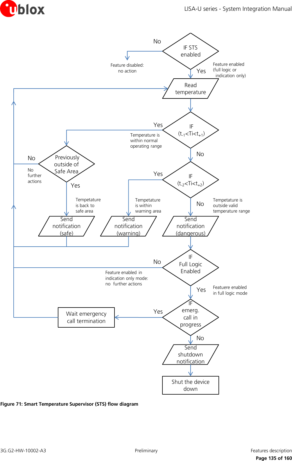
![LISA-U series - System Integration Manual 3G.G2-HW-10002-A3 Preliminary Features description Page 138 of 160 4. The visibility of multiple cells provides increased accuracy based on the intersection of areas of visibility. CellLocate is implemented using a set of two AT commands that allow configuration of the CellLocate service (AT+ULOCCELL) and requesting position according to the user configuration (AT+ULOC). The answer is provided in the form of an unsolicited AT command including latitude, longitude and estimated accuracy. The accuracy of the position estimated by CellLocate depends on the availability of historical observations in the specific area. 3.9.2 Hybrid positioning With u-blox Hybrid positioning technology, u-blox wireless devices can be triggered to provide their current position using either a u-blox GPS receiver or the position estimated from CellLocate. The choice depends on which positioning method provides the best and fastest solution according to the user configuration, exploiting the benefit of having multiple and complementary positioning methods. Hybrid positioning is implemented through a set of three AT commands that allow configuration of the GNSS receiver (AT+ULOCGNSS), configuration of the CellLocate service (AT+ULOCCELL), and requesting the position according to the user configuration (AT+ULOC). The answer is provided in the form of an unsolicited AT command including latitude, longitude and estimated accuracy (if the position has been estimated by CellLocate), and additional parameters if the position has been computed by the GNSS receiver. The configuration of mobile network cells does not remain static (e.g. new cells are continuously added or existing cells are reconfigured by the network operators). For this reason, when a Hybrid positioning method has been triggered and the GNSS receiver calculates the position, a database self-learning mechanism has been implemented so that these positions are sent to the server to update the database and maintain its accuracy. The use of hybrid positioning requires a connection via the DDC (I2C) bus between the LISA-U series wireless module and the u-blox GPS receiver (Refer to chapter 1.10). Refer to GPS Implementation Application Note [16] for the complete description of the feature. u-blox is extremely mindful of user privacy. When a position is sent to the CellLocate server u-blox is unable to track the SIM used or the specific device.](https://usermanual.wiki/u-blox/LISAU230/User-Guide-1727756-Page-138.png)
![LISA-U series - System Integration Manual 3G.G2-HW-10002-A3 Preliminary Handling and soldering Page 139 of 160 4 Handling and soldering No natural rubbers, no hygroscopic materials or materials containing asbestos are employed. 4.1 Packaging, shipping, storage and moisture preconditioning For information pertaining to reels and tapes, Moisture Sensitivity levels (MSD), shipment and storage information, as well as drying for preconditioning see the LISA-U1 series Data Sheet [1], the LISA-U2 series Data Sheet [2] and u-blox Package Information Guide [21]. The LISA-U series modules are Electro-Static Discharge (ESD) sensitive devices. Ensure ESD precautions are implemented during handling of the module. 4.2 Soldering 4.2.1 Soldering paste Use of "No Clean" soldering paste is strongly recommended, as it does not require cleaning after the soldering process has taken place. The paste listed in the example below meets these criteria. Soldering Paste: OM338 SAC405 / Nr.143714 (Cookson Electronics) Alloy specification: 95.5% Sn / 3.9% Ag / 0.6% Cu (95.5% Tin / 3.9% Silver / 0.6% Copper) 95.5% Sn / 4.0% Ag / 0.5% Cu (95.5% Tin / 4.0% Silver / 0.5% Copper) Melting Temperature: 217°C Stencil Thickness: 150 µm for base boards The final choice of the soldering paste depends on the approved manufacturing procedures. The paste-mask geometry for applying soldering paste should meet the recommendations in section 2.2.2 The quality of the solder joints on the connectors (’half vias’) should meet the appropriate IPC specification. 4.2.2 Reflow soldering A convection type-soldering oven is strongly recommended over the infrared type radiation oven. Convection heated ovens allow precise control of the temperature and all parts will be heated up evenly, regardless of material properties, thickness of components and surface color. Consider the "IPC-7530 Guidelines for temperature profiling for mass soldering (reflow and wave) processes, published 2001". Reflow profiles are to be selected according to the following recommendations. Failure to observe these recommendations can result in severe damage to the device! Preheat phase Initial heating of component leads and balls. Residual humidity will be dried out. Please note that this preheat phase will not replace prior baking procedures. Temperature rise rate: max 3°C/s If the temperature rise is too rapid in the preheat phase it may cause excessive slumping.](https://usermanual.wiki/u-blox/LISAU230/User-Guide-1727756-Page-139.png)
![LISA-U series - System Integration Manual 3G.G2-HW-10002-A3 Preliminary Handling and soldering Page 140 of 160 Time: 60 – 120 s If the preheat is insufficient, rather large solder balls tend to be generated. Conversely, if performed excessively, fine balls and large balls will be generated in clusters. End Temperature: 150 - 200°C If the temperature is too low, non-melting tends to be caused in areas containing large heat capacity. Heating/ reflow phase The temperature rises above the liquidus temperature of 217°C. Avoid a sudden rise in temperature as the slump of the paste could become worse. Limit time above 217°C liquidus temperature: 40 - 60 s Peak reflow temperature: 245°C Cooling phase A controlled cooling avoids negative metallurgical effects (solder becomes more brittle) of the solder and possible mechanical tensions in the products. Controlled cooling helps to achieve bright solder fillets with a good shape and low contact angle. Temperature fall rate: max 4°C / s To avoid falling off, modules should be placed on the topside of the motherboard during soldering. The soldering temperature profile chosen at the factory depends on additional external factors like choice of soldering paste, size, thickness and properties of the base board, etc. Exceeding the maximum soldering temperature and the maximum liquidus time limit in the recommended soldering profile may permanently damage the module. Preheat Heating Cooling[°C] Peak Temp. 245°C [°C]250 250Liquidus Temperature217 217200 20040 - 60 sEnd Temp.max 4°C/s150 - 200°C150 150max 3°C/s60 - 120 s100 Typical Leadfree 100Soldering Profile50 50Elapsed time [s] Figure 72: Recommended soldering profile LISA-U series modules must not be soldered with a damp heat process.](https://usermanual.wiki/u-blox/LISAU230/User-Guide-1727756-Page-140.png)
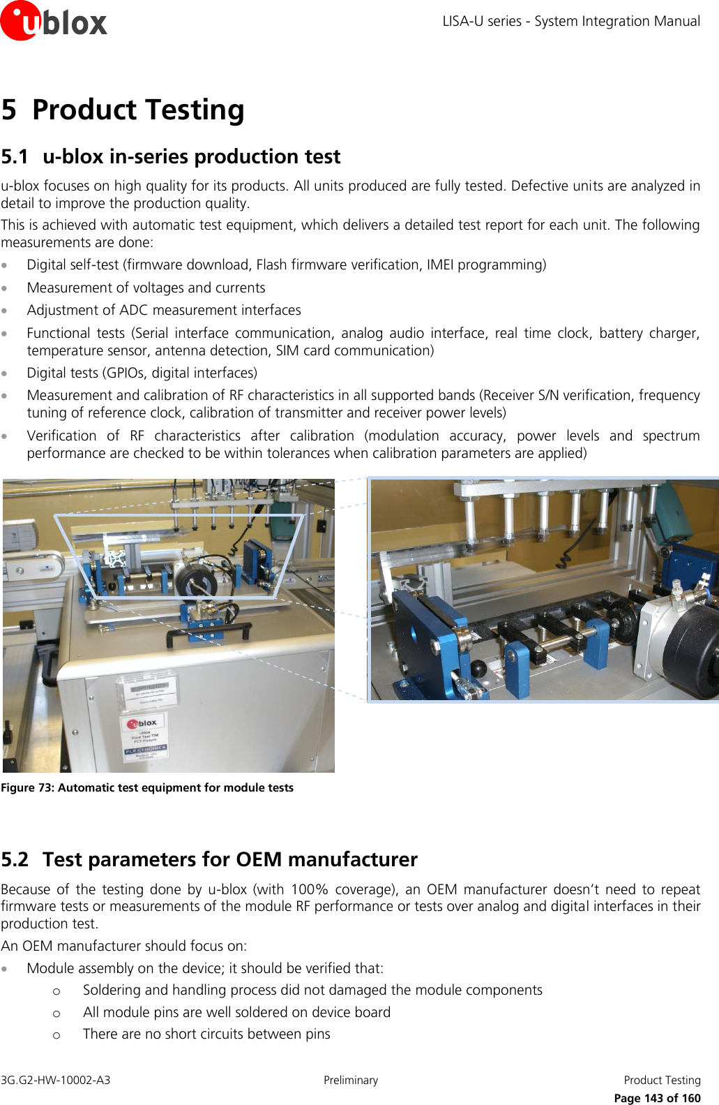
![LISA-U series - System Integration Manual 3G.G2-HW-10002-A3 Preliminary Product Testing Page 144 of 160 Component assembly on the device; it should be verified that: o Communication with host controller can be established o The interfaces between module and device are working o Overall RF performance test of the device including antenna Dedicated tests can be implemented to check the device. For example, the measurement of module current consumption when set in a specified status can detect a short circuit if compared with a “Golden Device” result. Module AT commands are used to perform functional tests (communication with host controller, check SIM card interface, check communication between module and GPS, GPIOs, etc.) and to perform RF performance tests. 5.2.1 ‘Go/No go’ tests for integrated devices A ‘Go/No go’ test is to compare the signal quality with a “Golden Device” in a position with excellent 2G/3G network coverage and after having dialed a call (refer to u-blox AT Commands Manual [3], AT+CSQ command: <rssi>, <ber> parameters). These kinds of test may be useful as a ‘go/no go’ test but not for RF performance measurements. This test is suitable to check the communication with host controller and SIM card, the audio and power supply functionality and verify if components at antenna interface are well soldered. 5.2.2 Functional tests providing RF operation Overall RF performance test of the device including antenna can be performed with basic instruments such as a standard spectrum analyzer and signal generator using an AT interface and AT+UTEST command. The AT+UTEST command gives a simple interface to set the module to Rx and Tx test modes ignoring 2G/3G signaling protocol. The command can set the module: In transmitting mode in a specified channel and power level in all supported modulation schemes (single slot GMSK, single slot 8PSK, WCDMA) and bands 2G, 3G In receiving mode in a specified channel to returns the measured power level in all supported bands 2G, 3G The AT+UTEST command used to perform these functional tests is available on all LISA-U series modules versions except LISA-U1xx-00. Refer to u-blox AT Commands Manual [3], for AT+UTEST command syntax description. Refer to End user test Application Note [20], for AT+UTEST command user guide, limitations and examples of use.](https://usermanual.wiki/u-blox/LISAU230/User-Guide-1727756-Page-144.png)
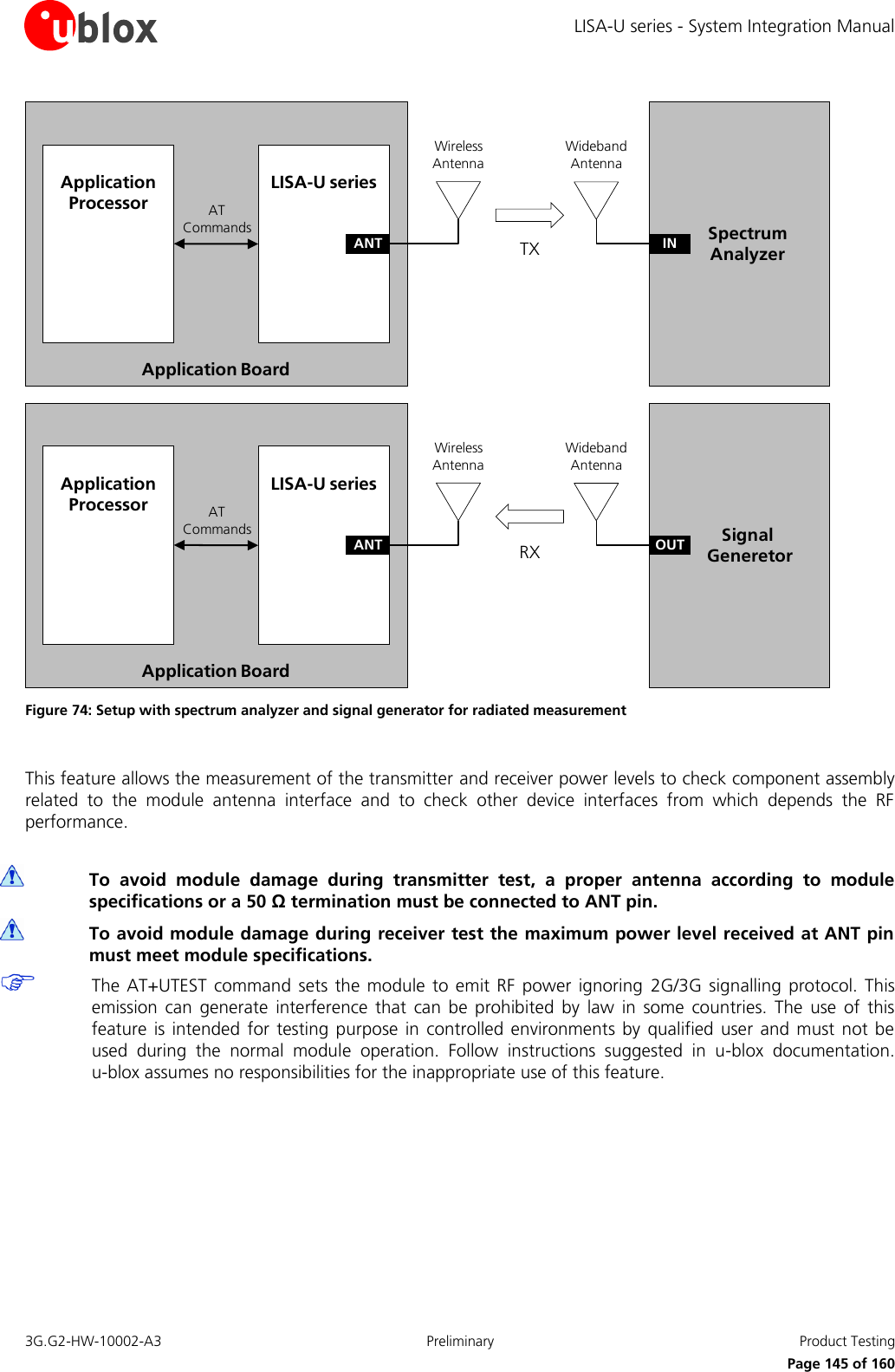
![LISA-U series - System Integration Manual 3G.G2-HW-10002-A3 Preliminary Appendix Page 148 of 160 Check LISA-U2 series Software Requirements Not all of the functionalities available with LISA-U1 series modules are supported by all the LISA-U2 series modules versions. These include: o Analog Audio Interfaces are not supported by all LISA-U2 series modules o Digital Audio Interfaces are supported by all LISA-U2 series modules versions except LISA-U200-00 o Embedded AssistNow Software, GPS via Modem, Hybrid positioning and CellLocate functionalities are supported by all LISA-U2 series modules versions except LISA-U200-00 o In-band modem is supported by all LISA-U2 series modules versions except LISA-U200-00 Check section A.2 Software migration. A.2 Software migration A.2.1 Software migration from LISA-U1 series to LISA-U2 series wireless modules Software migration from LISA-U1 series to LISA-U2 series wireless modules is a straightforward procedure. Nevertheless there are some differences to be considered with firmware version. Like predecessors, LISA-U2 series wireless module supports AT commands according to 3GPP standards: TS 27.007 [5], TS 27.005 [6], TS 27.010 [7] and the u-blox AT command extension. Backward compatibility has been maintained as far as possible. For the complete list of supported AT commands and their syntax see u-blox AT Commands Manual [3]. A.3 Hardware migration A.3.1 Hardware migration from LISA-U1 series to LISA-U2 series wireless modules LISA-U2 series wireless modules have been designed with backward compatibility in mind but some minor differences were unavoidable. These minor differences will however not be relevant for the majority of the LISA-U1 series designs. Clean and stable supply is required by LISA-U2 as by LISA-U1 series: low ripple and low voltage drop must be guaranteed at VCC pins. The voltage provided has to be within the normal operating range limits to allow module switch-on and has to be above the minimum limit of the extended operating range to avoid module switch-off. Consider that there are large current spikes in connected mode, when a GSM call is enabled. LISA-U2 series provide wider VCC input voltage range compared to LISA-U1 series. The ANT pin has 50 Ω nominal characteristic impedance and must be connected to the antenna through a 50 Ω transmission line to allow transmission and reception of radio frequency (RF) signals in the 2G and 3G operating bands. The recommendations of the antenna producer for correct installation and deployment (PCB layout and matching circuitry) must be followed. The antenna and the whole RF circuit must provide optimal radiating characteristics on the entire supported bands: note that LISA-U2 supports different 3G bands in comparison to LISA-U1 series wireless modules. LISA-U230 modules provide the RF antenna input for Rx diversity on the pin 74 (named ANT_DIV): it has an impedance of 50 Ω. The same pad is a reserved pin on LISA-U1 series and LISA-U200 modules. Analog audio interfaces are not supported by LISA-U2 series modules, but a second 4-wire I2S digital audio interface is provided instead of the 4 analog audio pins on all LISA-U2 series modules versions except LISA-U200-00. The same 4 pins can be configured as GPIO on all LISA-U2 series modules versions.](https://usermanual.wiki/u-blox/LISAU230/User-Guide-1727756-Page-148.png)
![LISA-U series - System Integration Manual 3G.G2-HW-10002-A3 Preliminary Appendix Page 149 of 160 Digital audio interfaces are supported by all LISA-U2 series modules versions except LISA-U200-00: the relative pins are configured as pad disabled on LISA-U200-00 version. PWR_ON and RESET_N input voltage thresholds are slightly changed in comparison to LISA-U1 series modules, but this is not relevant driving PWR_ON and RESET_N inputs by open drain / collector drivers as recommended. LISA-U2xx-01 modules can be switched off forcing PWR_ON pin to the low level for at least 1 s. V_BCKP operating characteristics are slightly changed in comparison to LISA-U1 series modules. The 5 pins of the SPI / IPC Serial Interface can be configured as GPIOs on LISA-U2xx-01 modules. LISA-U2 series wireless modules are SMT modules and come in the same compact form factor of LISA-U1 series, featuring Leadless Chip Carrier (LCC) packaging technology. Additional signals keep-out area must be implemented on the top layer of the application board, below LISA-U2 modules, due to GND opening on module bottom layer. Detailed pinout and layout comparisons between LISA-U1 series and LISA-U2 series modules, with remarks for migration, are provided in the subsections A.3.2 and A.3.3. For more information regarding LISA-U1 and LISA-U2 series modules electrical characteristics refer to LISA-U1 series Data Sheet [1] and LISA-U2 series Data Sheet [2]. A.3.2 Pin-out comparison LISA-U1 series vs. LISA-U2 series 65646362616059585756555453525150494847464544434241GNDVCCVCCVCCGNDSPI_MRDYSPI_SRDYSPI_MISOSPI_MOSISPI_SCLKRSVD / SPK_NGNDRSVD / SPK_PRSVDGPIO5VSIMSIM_RSTSIM_IOSIM_CLKSDASCLRSVD / I2S_RXDRSVD / I2S_CLKRSVD / I2S_TXDRSVD / I2S_WA12345678910111213141516171819202122232425V_BCKPGNDV_INTRSVDGNDGNDGNDDSRRIDCDDTRGNDRTSCTSTXDRXDGNDVUSB_DETPWR_ONGPIO1GPIO2RESET_NGPIO3GPIO4GND2627USB_D-USB_D+4039RSVD / MIC_PRSVD / MIC_N2829303132333435363738GNDGNDGNDGNDGNDGNDGNDGNDGNDGNDGND 7675747372717069686766GNDRSVDGNDGNDGNDGNDGNDANTGNDGNDGNDLISA-U1Top View Figure 75: LISA-U1 series pin assignment 65646362616059585756555453525150494847464544434241GNDVCCVCCVCCGNDSPI_MRDY / GPIO14SPI_SRDY / GPIO13SPI_MISO / GPIO12SPI_MOSI / GPIO11SPI_SCLK / GPIO10GPIO9 / I2S1_WAGNDGPIO8 / I2S1_CLKRSVD / CODEC_CLKGPIO5VSIMSIM_RSTSIM_IOSIM_CLKSDASCLRSVD / I2S_RXDRSVD / I2S_CLKRSVD / I2S_TXDRSVD / I2S_WA12345678910111213141516171819202122232425V_BCKPGNDV_INTRSVDGNDGNDGNDDSRRIDCDDTRGNDRTSCTSTXDRXDGNDVUSB_DETPWR_ONGPIO1GPIO2RESET_NGPIO3GPIO4GND2627USB_D-USB_D+4039GPIO7 / I2S1_TXDGPIO6 / I2S1_RXD2829303132333435363738GNDGNDGNDGNDGNDGNDGNDGNDGNDGNDGND 7675747372717069686766GNDRSVD / ANT_DIVGNDGNDGNDGNDGNDANTGNDGNDGNDLISA-U2Top View Figure 76: LISA-U2 series pin assignment (highlighted name/function changes)](https://usermanual.wiki/u-blox/LISAU230/User-Guide-1727756-Page-149.png)
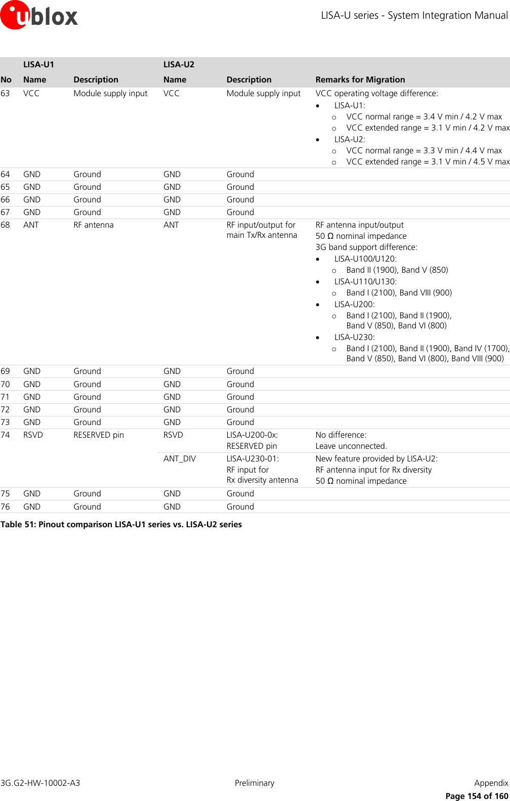
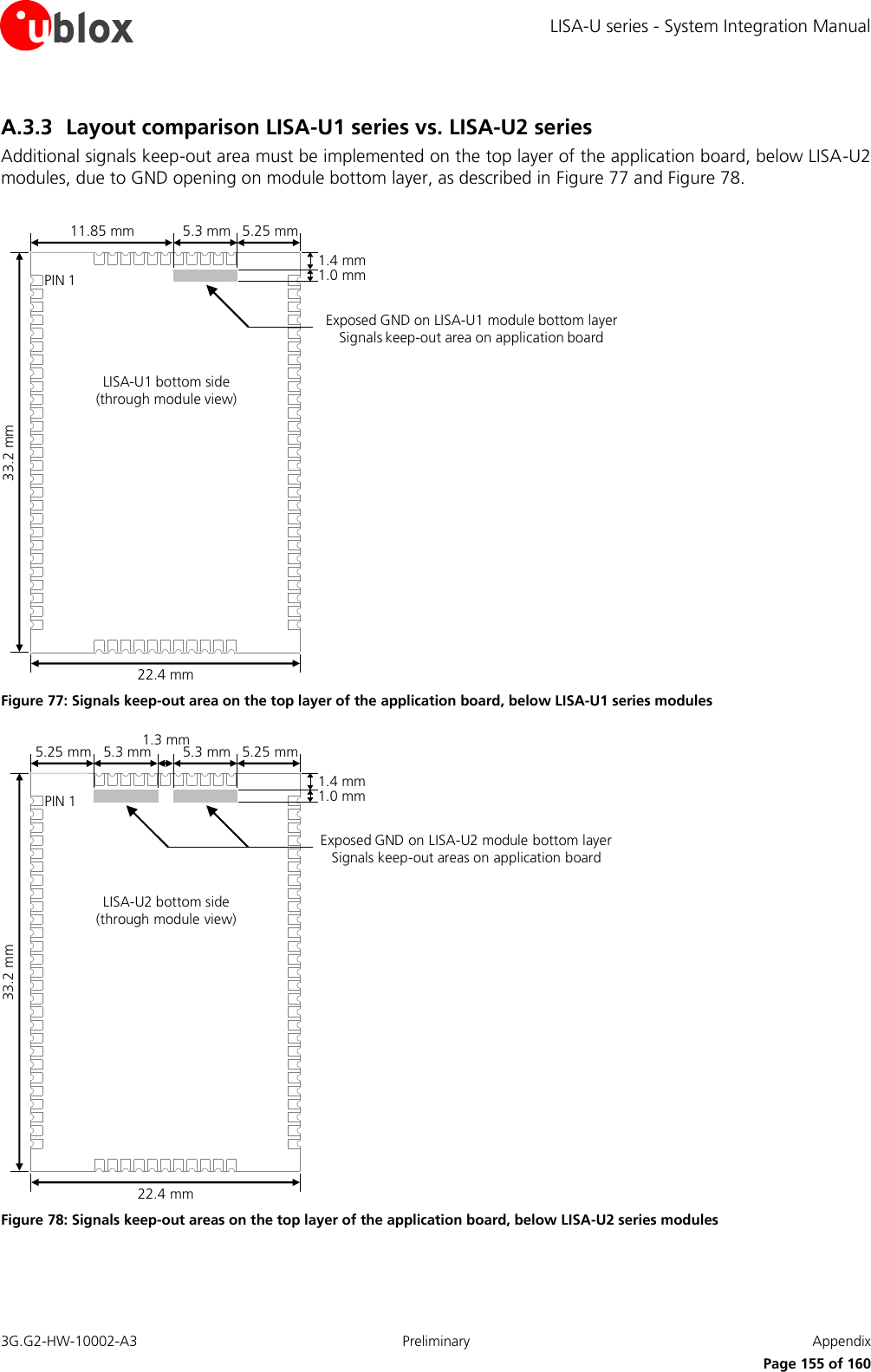
![LISA-U series - System Integration Manual 3G.G2-HW-10002-A3 Preliminary Related documents Page 158 of 160 Related documents [1] u-blox LISA-U1 series Data Sheet, Docu No 3G.G1-HW-10001 [2] u-blox LISA-U2 series Data Sheet, Docu No 3G.G1-HW-11004 [3] u-blox AT Commands Manual, Docu No WLS-SW-11000 [4] ITU-T Recommendation V.24, 02-2000. List of definitions for interchange circuits between data terminal equipment (DTE) and data circuit-terminating equipment (DCE). http://www.itu.int/rec/T-REC-V.24-200002-I/en [5] 3GPP TS 27.007 - AT command set for User Equipment (UE) (Release 1999) [6] 3GPP TS 27.005 - Use of Data Terminal Equipment - Data Circuit terminating; Equipment (DTE - DCE) interface for Short Message Service (SMS) and Cell Broadcast Service (CBS) (Release 1999) [7] 3GPP TS 27.010 - Terminal Equipment to User Equipment (TE-UE) multiplexer protocol (Release 1999) [8] Universal Serial Bus Revision 2.0 specification, http://www.usb.org/developers/docs/ [9] I2C-Bus Specification Version 2.1 Philips Semiconductors (January 2000), http://www.nxp.com/acrobat_download/literature/9398/39340011_21.pdf [10] CENELEC EN 61000-4-2 (2001): "Electromagnetic compatibility (EMC) - Part 4-2: Testing and measurement techniques - Electrostatic discharge immunity test". [11] ETSI EN 301 489-1 V1.8.1: “Electromagnetic compatibility and Radio spectrum Matters (ERM); ElectroMagnetic Compatibility (EMC) standard for radio equipment and services; Part 1: Common technical requirements” [12] ETSI EN 301 489-7 V1.3.1 “Electromagnetic compatibility and Radio spectrum Matters (ERM); ElectroMagnetic Compatibility (EMC) standard for radio equipment and services; Part 7: Specific conditions for mobile and portable radio and ancillary equipment of digital cellular radio telecommunications systems (GSM and DCS)“ [13] ETSI EN 301 489-24 V1.4.1 "Electromagnetic compatibility and Radio spectrum Matters (ERM); ElectroMagnetic Compatibility (EMC) standard for radio equipment and services; Part 24: Specific conditions for IMT-2000 CDMA Direct Spread (UTRA) for Mobile and portable (UE) radio and ancillary equipment" [14] 3GPP TS 26.267 - Technical Specification Group Services and System Aspects; eCall Data Transfer; In-band modem solution; General description (Release 9) [15] GSM Mux Implementation Application Note, Docu No WLS-CS-11002 [16] GPS Implementation Application Note, Docu No GSM.G1-CS-09007 [17] Firmware Update Application Note, Docu No WLS-CS-11001 [18] SPI Interface application Note, Docu No 3G.G2-CS-11000 [19] 3GPP TS 23.060 - Technical Specification Group Services and System Aspects; General Packet Radio Service (GPRS); Service description [20] End user test Application Note, Docu No TBD [21] u-blox Package Information Guide, Docu. No GPS-X-11004 Some of the above documents can be downloaded from u-blox web-site (http://www.u-blox.com).](https://usermanual.wiki/u-blox/LISAU230/User-Guide-1727756-Page-158.png)