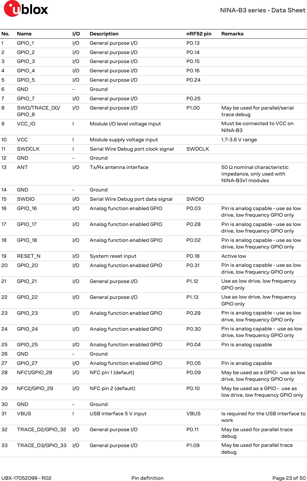
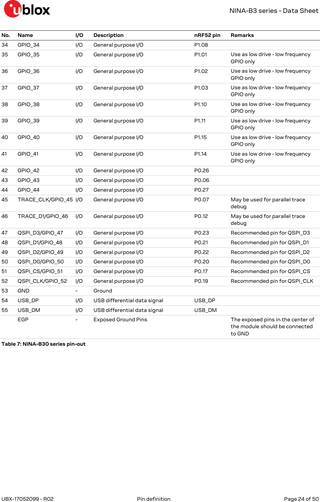
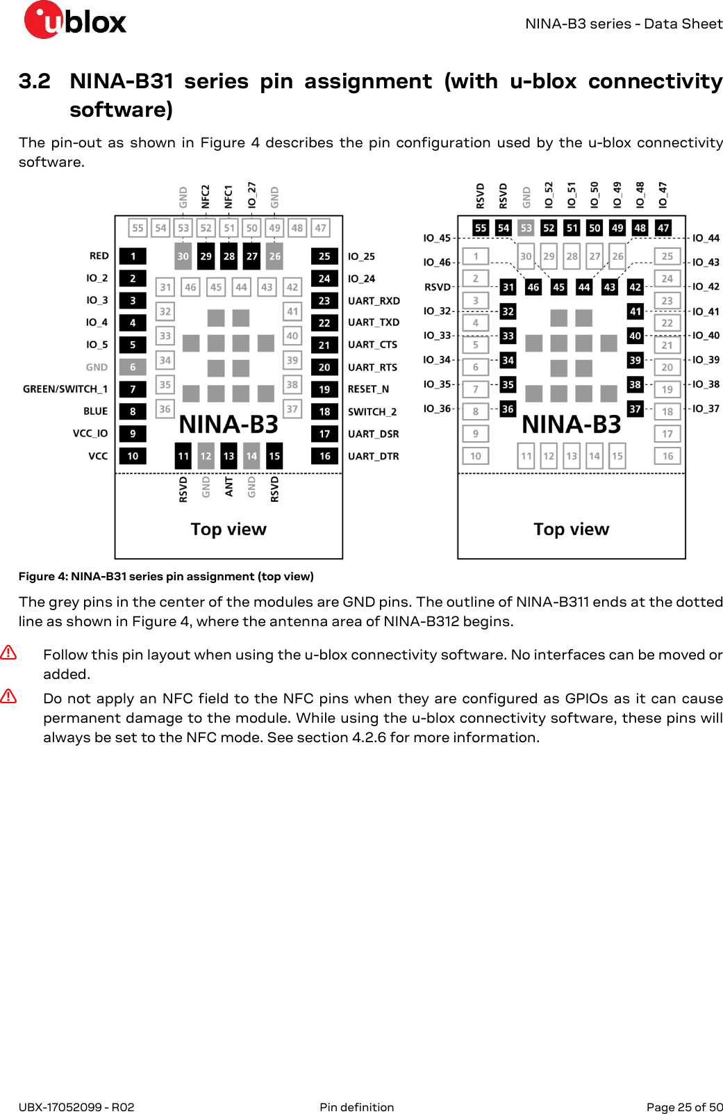
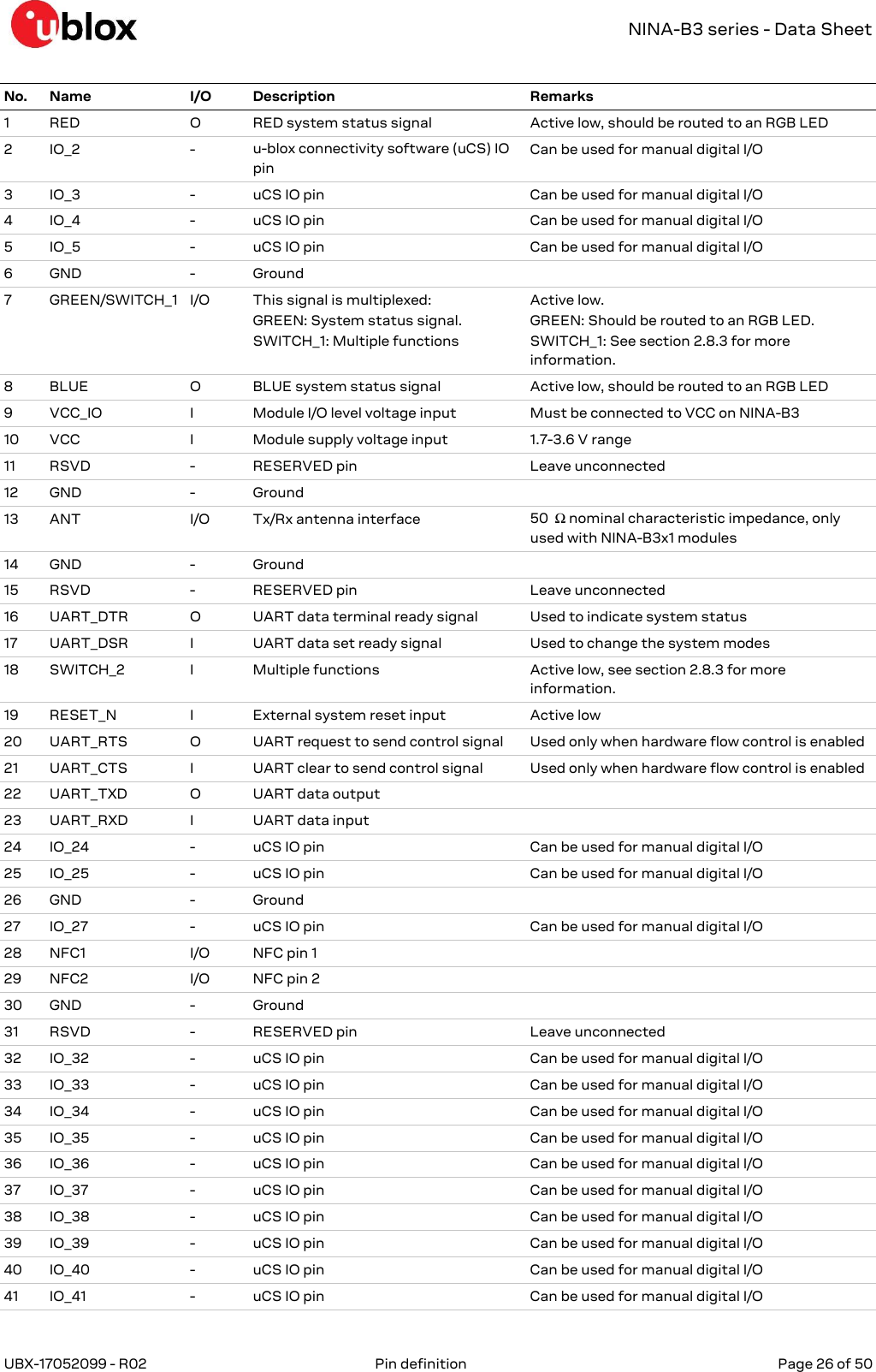
u blox NINAB31 Wireless Communication System Module User Manual Product Name
u-blox AG Wireless Communication System Module Product Name
UserManual.wiki
>
u blox
>
NINAB31 User Manual
>
user manual
Contents
1.
user manual
2.
UserManual_SCOUT220-IS and SCOUT240-IS Portable Data Collectors Datasheet - 109M
user manual
Navigation menu
Upload a User Manual
Namespaces
Wiki Guide
HTML
PDF
Info
Views
User Manual
Discussion / Help
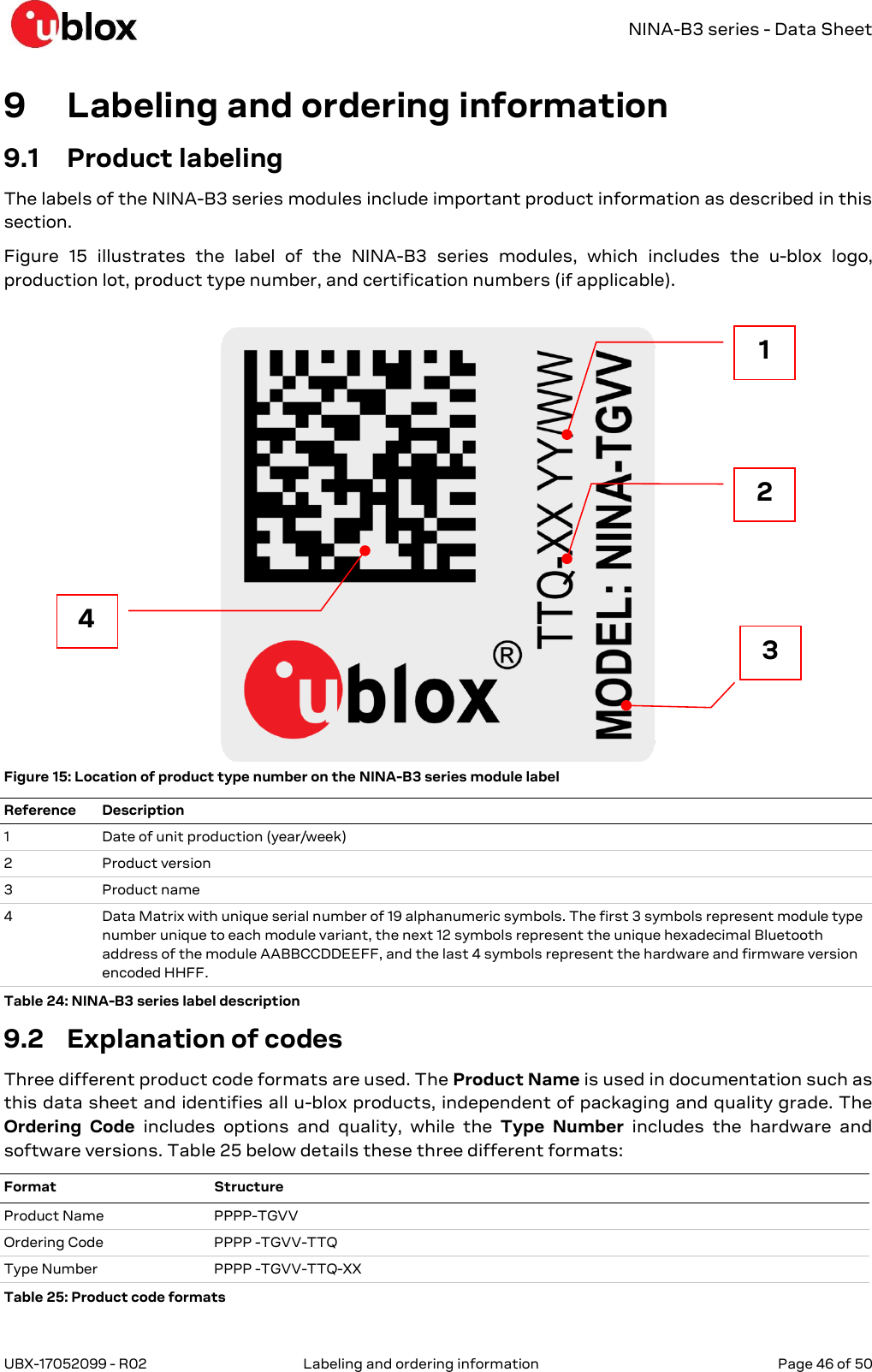
Navigation
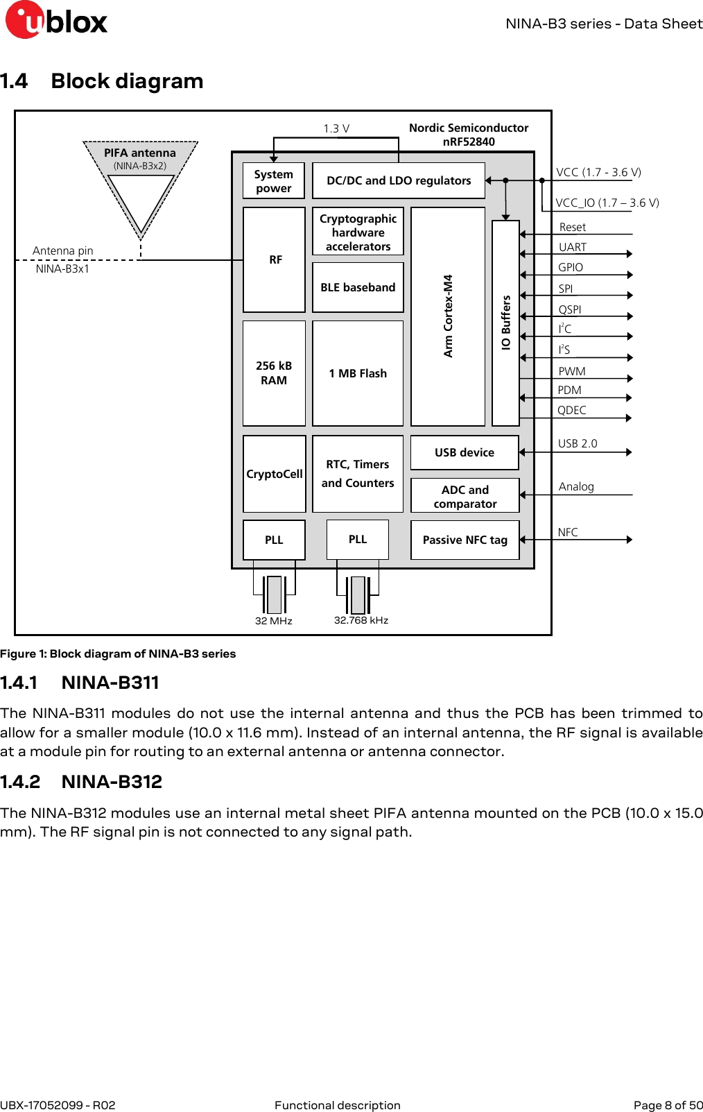
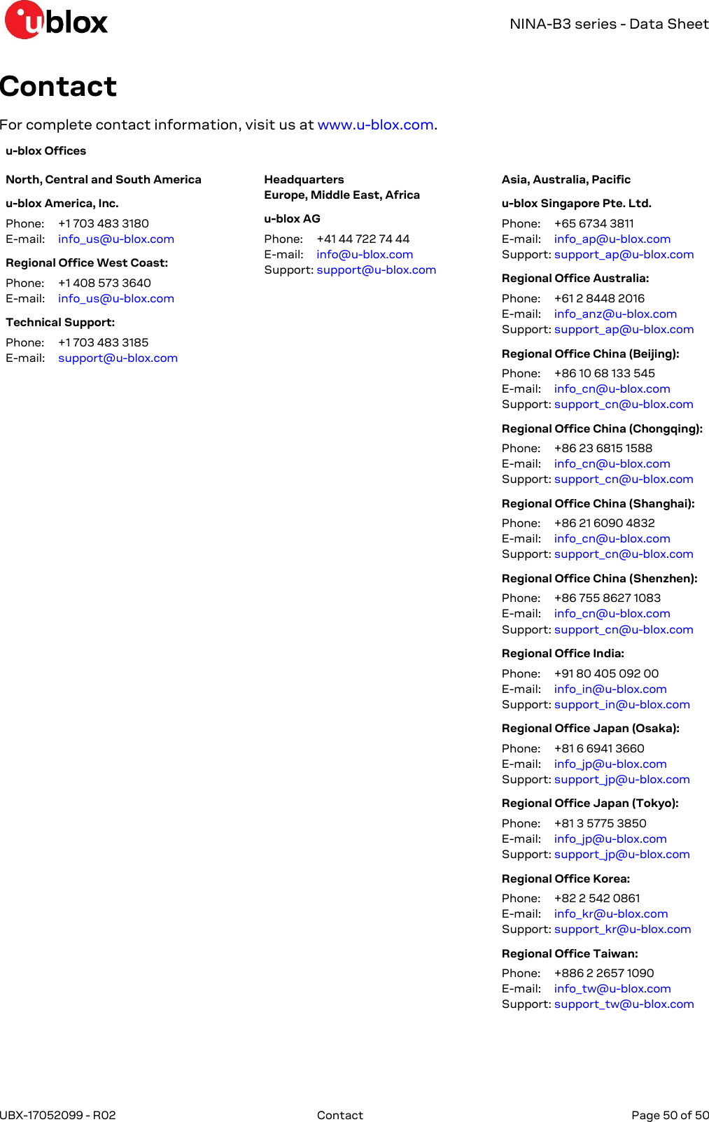
![NINA-B3 series - Data Sheet UBX-17052099 - R02 Functional description Page 10 of 50 1.7.1 u-blox connectivity software The NINA-B31 series modules are pre-flashed with u-blox connectivity software. The u-blox connectivity software enables use of the u-blox Low Energy Serial Port Service, controlled by AT commands over the UART interface. The NINA-B31 modules can be configured using the u-blox s-center evaluation software, which can be downloaded from the u-blox website and is available free of charge. Much more information on the features and capabilities of the u-blox connectivity software and how to use it can be found in the u-blox Short Range AT Commands Manual [2]. 1.7.2 Open CPU The open CPU architecture in the NINA-B30 series modules allows you to build your own applications. u-blox recommends the following development approaches to speed up the process: 1.7.2.1 Nordic SDK The Nordic Semiconductors nRF5 SDK provides a rich and well-tested software development environment for nRF52 based devices. It includes a broad selection of drivers, libraries, and example applications. It also includes other radio stacks. The NINA-B3 series modules are only certified for use with the S140 Bluetooth Low Energy SoftDevice. If you would like to use another 2.4 GHz radio protocol, contact u-blox support for your area as listed in the Contact section. 1.7.2.2 Wirepas connectivity software The NINA-B30 series modules can also be used together with the Wirepas software stack. This will enable the NINA-B30 module to be used in a large scale mesh environment. The Wirepas connectivity software is a third party licensed software from Wirepas. For more information about the Wirepas connectivity software, contact the u-blox support for your area as listed in the Contact section or contact Wirepas directly. 1.8 Bluetooth device address Figure 2: NINA-B3 software structure and available software options NINA-B3 Software structure Bootloader Radio Stack Application NINA-B31 series NINA-B30 series options Nordic S140 SoftDevice u-blox connectivity software Nordic SDK Wirepas mesh Connectivity Software + SDK](https://usermanual.wiki/u-blox/NINAB31.user-manual/User-Guide-3999355-Page-10.png)
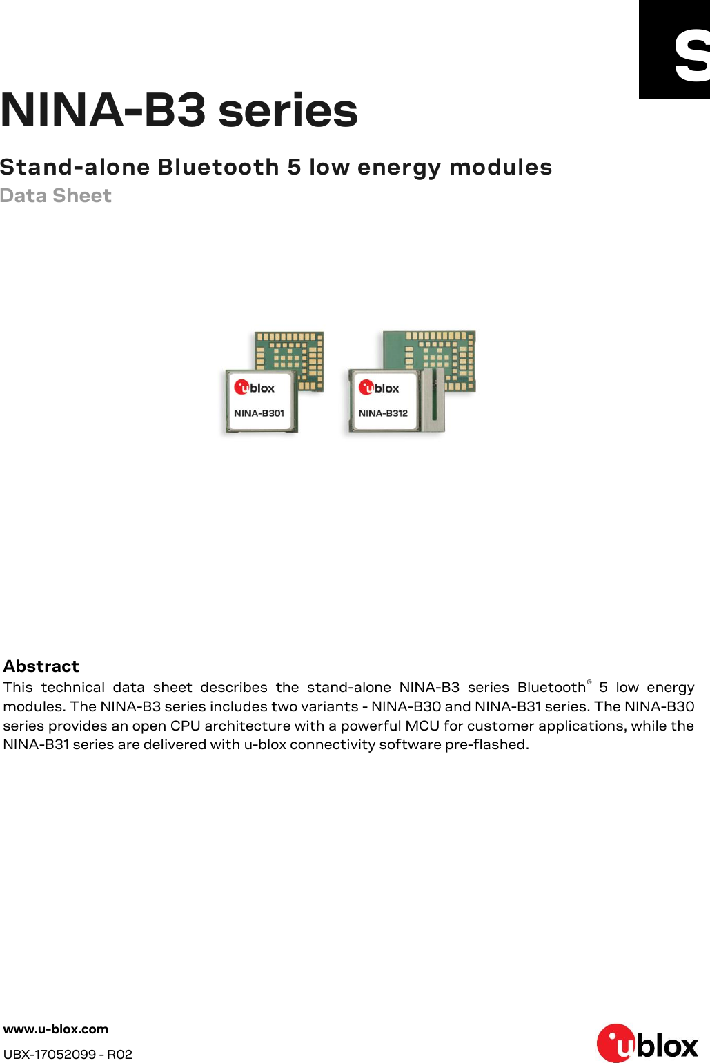
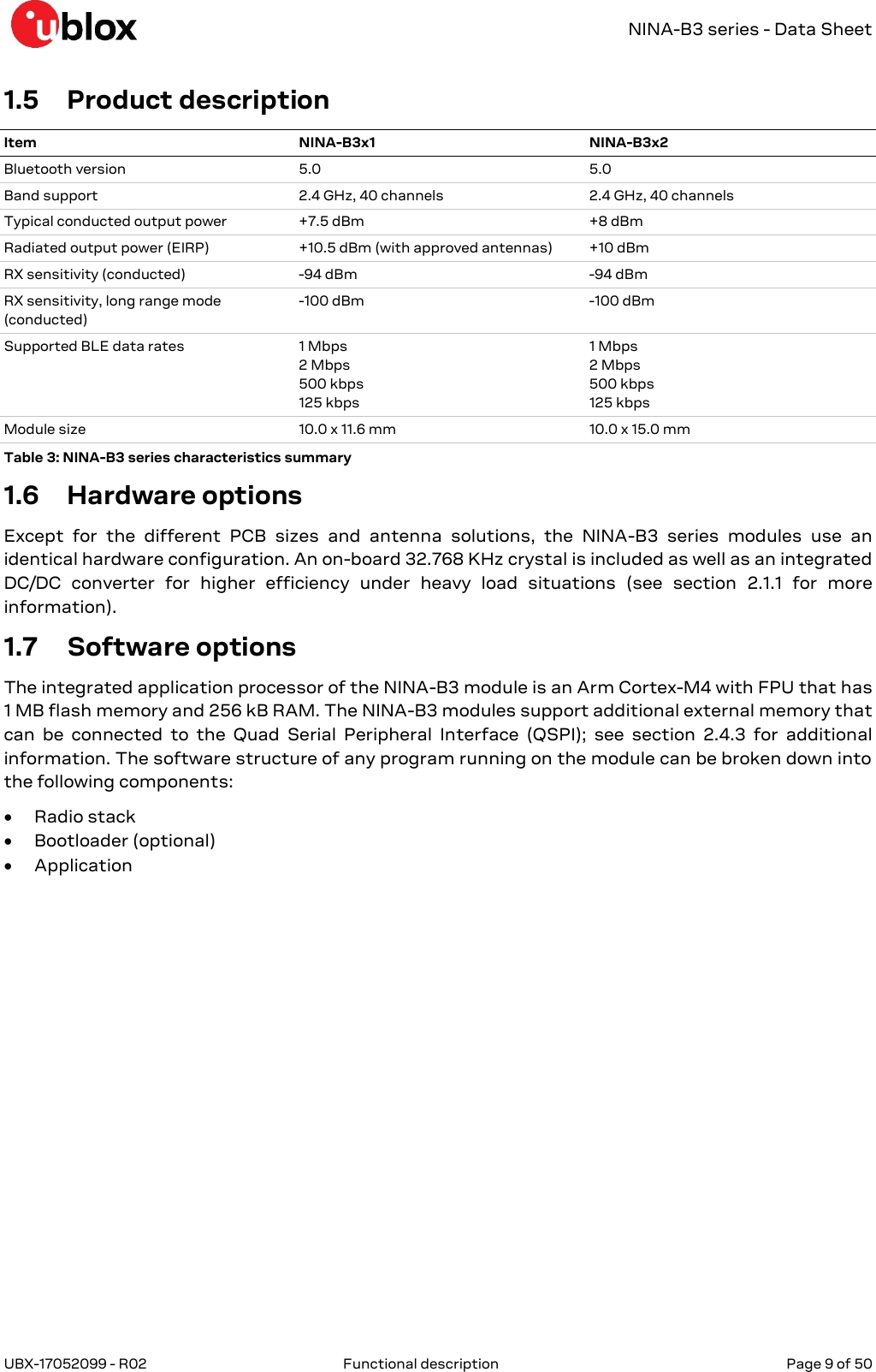
![NINA-B3 series - Data Sheet UBX-17052099 - R02 Interfaces Page 20 of 50 Function Description Default NINA pin Configurable GPIOs General purpose input Digital input with configurable pull-up, pull-down, edge detection and interrupt generation Any General purpose output Digital output with configurable drive strength, push-pull, open collector or open emitter output Any Pin disabled Pin is disconnected from the input and output buffers All* Any Timer/ counter High precision time measurement between two pulses/ Pulse counting with interrupt/event generation Any Interrupt/ Event trigger Interrupt/event trigger to the software application/ Wake up event Any HIGH/LOW/Toggle on event Programmable digital level triggered by internal or external events without CPU involvement Any ADC input 8/10/12/14-bit analog to digital converter Any analog Analog comparator input Compare two voltages, capable of generating wake-up events and interrupts Any analog PWM output Output simple or complex pulse width modulation waveforms Any Connection status indication Indicates if a BLE connection is maintained BLUE** Any * = If left unconfigured ** = While using the u-blox connectivity software Table 5: GPIO custom functions configuration 2.8 u-blox connectivity software features This section describes some of the system related features in the u-blox connectivity software. For additional information, see the u-blox Short Range AT Commands Manual [2]. 2.8.1 u-blox Serial Port Service (SPS) The serial port service feature enables serial port emulation over Bluetooth low energy. 2.8.2 System status signals The RED, GREEN, and BLUE pins are used to signal the system status as shown in Table 6. They are active low and are intended to be routed to an RGB LED. Mode Status RGB LED Color RED GREEN BLUE Data mode/Extended Data mode (EDM) IDLE Green HIGH LOW HIGH Command mode IDLE Orange LOW LOW HIGH EDM/Data mode, Command mode CONNECTING Purple LOW HIGH LOW EDM/Data mode, Command mode CONNECTED** Blue HIGH HIGH LOW * = LED flashes on data activity Table 6: System status indication ☞ The CONNECTING and CONNECTED statuses indicate u-blox SPS connections. 2.8.3 System control signals The following input signals are used to control the system: RESET_N is used to reset the system. See section 2.3.5 for detailed information. If SWITCH_2 is driven low during start up, the UART serial settings are restored to their default values. The SWITCH_2 can be used to open a Bluetooth LE connection with a peripheral device.](https://usermanual.wiki/u-blox/NINAB31.user-manual/User-Guide-3999355-Page-20.png)
![NINA-B3 series - Data Sheet UBX-17052099 - R02 Interfaces Page 21 of 50 If both SWITCH_1 and SWITCH_2 are driven low during start up, the system will enter bootloader mode. If both SWITCH_1 and SWITCH_2 are driven low during start up and held low for 10 seconds, the system will exit the bootloader mode and restore all settings to their factory default. 2.8.4 UART signals In addition to the normal RXD, TXD, CTS, and RTS signals, the u-blox connectivity software adds the DSR and DTR pins to the UART interface. Note that they are not used as originally intended, but to control the state of the NINA module. For example, depending on the current configuration: The DSR pin can be used to: Enter the command mode Disconnect and/or toggle connectable status Enable/disable the rest of the UART interface Enter/wake up from the sleep mode The DTR pin can be used to indicate: The System mode If the SPS peers are connected If a Bluetooth LE bonded device is connected A Bluetooth LE GAP connection ☞ See the u-blox Short Range AT Commands Manual [2] for more information. 2.9 Debug interfaces 2.9.1 SWD The NINA-B30 series modules provide an SWD interface for flashing and debugging. The SWD interface consists of two pins - SWDCLK and SWDIO. The SWD interface is disabled on the NINA-B31 series modules. 2.9.2 Trace – Serial Wire Output A serial trace option is available on the NINA-B30 series modules as an additional pin- SWO. The Serial Wire Output (SWO) is used to: Support printf style debugging Trace OS and application events Emit diagnostic system information A debugger that supports Serial Wire Viewer (SWV) is required. 2.9.3 Parallel Trace The NINA-B30 series modules support parallel trace output as well. This allows output from the Embedded Trace Macrocell (ETM) and Instrumentation Trace Macrocell (ITM) embedded in the Arm Cortex-M4 core of the nRF52840 chip in the NINA-B3. The ETM trace data allows a user to record exactly how the application goes through the CPU instructions in real time. The parallel trace interface uses 1 clock signal and 4 data signals respectively - TRACE_CLK, TRACE_D0, TRACE_D1, TRACE_D2 and TRACE_D3.](https://usermanual.wiki/u-blox/NINAB31.user-manual/User-Guide-3999355-Page-21.png)
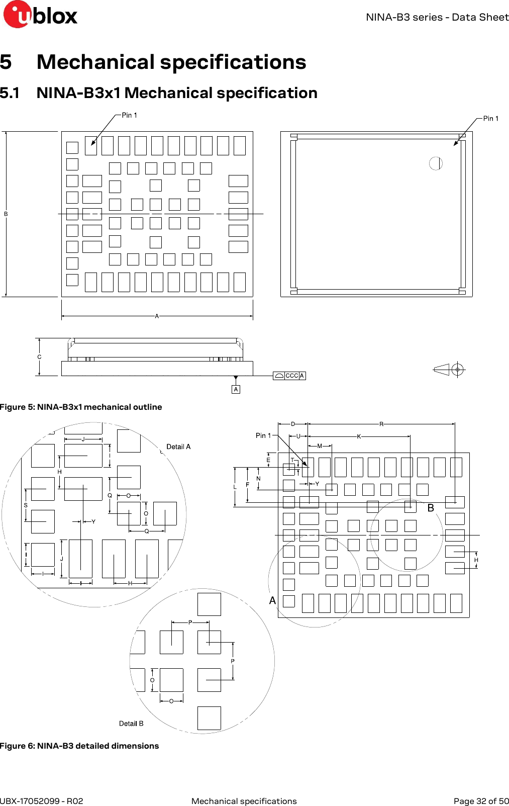
![NINA-B3 series - Data Sheet UBX-17052099 - R02 Mechanical specifications Page 33 of 50 Parameter Description Typical [mm] [mil] Tolerance [mm] [mil] A Module PCB length 11.6 B Module PCB width 10.0 C Module thickness 2.23 ccc Seating plane coplanarity 0.10 D Horizontal edge to pin no. 1 center 1.80 E Vertical edge to pin no. 1 center 0.875 F Vertical pin no. 1 center to lateral pin center 2.125 H Lateral and antenna row pin to pin pitch 1.00 I Lateral, antenna row and outer pin width 0.70 J Lateral and antenna row pin length 1.15 K Horizontal pin no. 1 center to central pin center 6.225 L Vertical pin no. 1 center to central pin center 2.40 M Horizontal pin no. 1 center to inner row pin center 1.45 N Vertical pin no. 1 center to inner row pin center 1.375 O Central, inner and outer row pin width and length 0.70 P Central pin to central pin pitch 1.15 Q Inner row pin to pin pitch 1.10 R Horizontal pin no. 1 center to antenna row pin center 8.925 S Outer row pin to pin pitch 1.0 T Vertical pin no. 1 center to outer row pin center 0.125 U Horizontal pin no. 1 center to outer row pin center 1.15 Y Horizontal pin no. 1 center to lateral pin center 0.075 Module weight [g] <1.0 Table 20: NINA-B3x1 mechanical outline data](https://usermanual.wiki/u-blox/NINAB31.user-manual/User-Guide-3999355-Page-33.png)
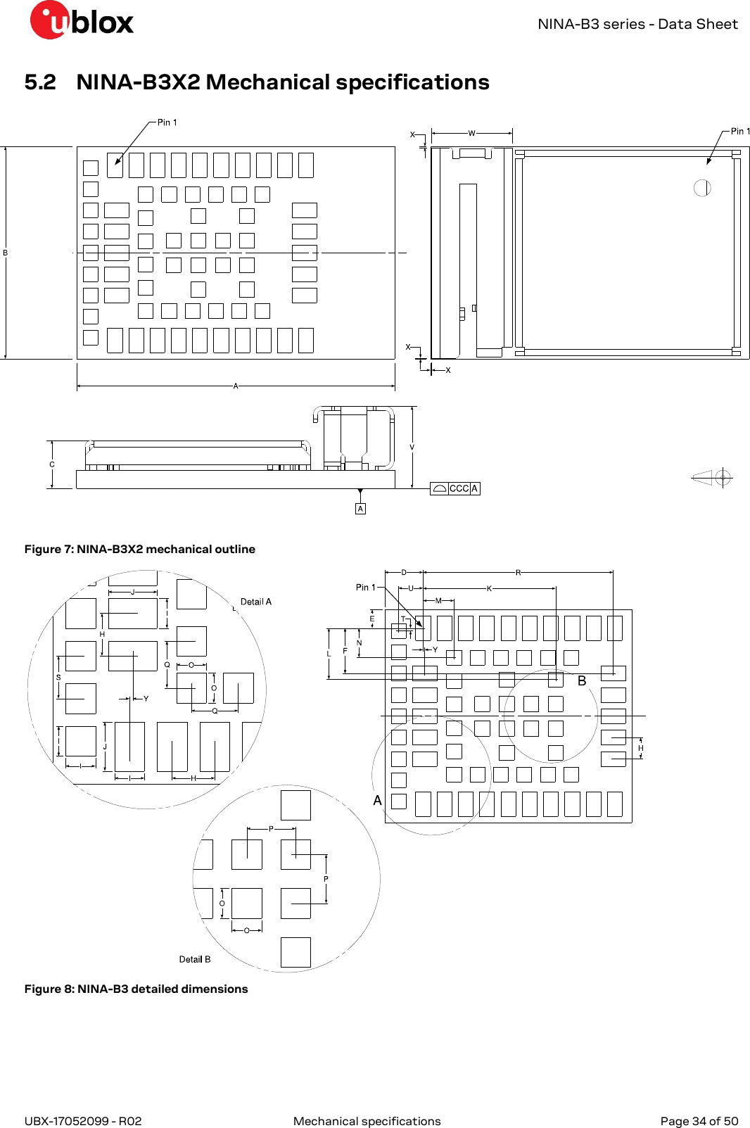
![NINA-B3 series - Data Sheet UBX-17052099 - R02 Mechanical specifications Page 35 of 50 Parameter Description Typical [mm] [mil] Tolerance [mm] [mil] A Module PCB length 15.0 B Module PCB width 10.0 C Module thickness 2.23 ccc Seating plane coplanarity 0.10 D Horizontal edge to pin no. 1 center 1.80 E Vertical edge to pin no. 1 center 0.875 F Vertical pin no. 1 center to lateral pin center 2.125 H Lateral and antenna row pin to pin pitch 1.00 I Lateral, antenna row and outer pin width 0.70 J Lateral and antenna row pin length 1.15 K Horizontal pin no. 1 center to central pin center 6.225 L Vertical pin no. 1 center to central pin center 2.40 M Horizontal pin no. 1 center to inner row pin center 1.45 N Vertical pin no. 1 center to inner row pin center 1.375 O Central, inner and outer row pin width and length 0.70 P Central pin to central pin pitch 1.15 Q Inner row pin to pin pitch 1.10 R Horizontal pin no. 1 center to antenna row pin center 8.925 S Outer row pin to pin pitch 1.0 T Vertical pin no. 1 center to outer row pin center 0.125 U Horizontal pin no. 1 center to outer row pin center 1.15 V PCB and antenna thickness 3.83 W Module antenna width 3.8 X Antenna overhang outside module outline on any side 0.0 +0.60 Y Horizontal pin no. 1 center to lateral pin center 0.075 Module weight [g] <1.0 Table 21: NINA-B3X2 mechanical outline data](https://usermanual.wiki/u-blox/NINAB31.user-manual/User-Guide-3999355-Page-35.png)
![NINA-B3 series - Data Sheet UBX-17052099 - R02 Qualification and approvals Page 37 of 50 6.2.1.1 FCC Compliance The NINA-B3 modules are for OEM integrations only. The end-product will be professionally installed in such manner that only the authorized antennas can be used. For NINA-B301 and NINA-B311, an external antenna connector (U.FL. connector) reference design is available and must be followed to comply with the NINA-B30/NINA-B31 FCC/IC modular approval (see the NINA-B3 Series System Integration Manual [3]). 6.2.1.2 FCC statement This device complies with Part 15 of the FCC Rules. Operation is subject to the following two conditions: 1. This device may not cause harmful interference, and 2. This device must accept any interference received, including interference that may cause undesired operation. This equipment has been tested and found to comply with the limits for a Class B digital device, pursuant to Part 15 of the FCC Rules. These limits are designed to provide reasonable protection against harmful interference in a residential installation. This equipment generates, uses and can radiate radio frequency energy and, if not installed and used in accordance with the instructions, may cause harmful interference to radio communications. However, there is no guarantee that the interference will not occur in a particular installation. If this equipment does cause harmful interference to radio or television reception, which can be determined by turning the equipment off and on, the user is encouraged to try to correct the interference by one or more of the following measures: Reorient or relocate the receiving antenna Increase the separation between the equipment and receiver Connect the equipment into an outlet on a circuit different from that to which the receiver is connected. Consult the dealer or an experienced radio/TV technician for help. 6.2.2 RF-exposure statement 6.2.2.1 IC Compliance This equipment complies with the requirements of IC RSS-102 issue 5 radiation exposure limits set forth for an uncontrolled environment. Having a separation distance of minimum 15 mm between the user and/or bystander and the antenna and /or radiating element ensures that the output power (e.i.r.p.) of NINA-B3 is below the SAR evaluation Exemption limits defined in RSS-102 issue 5. 6.2.2.2 FCC Compliance This device complies with the FCC radiation exposure limits set forth for an uncontrolled environment. Having a separation distance of minimum 10 mm between the user and/or bystander and the antenna and /or radiating element ensures that max output power of NINA-B3 is below the SAR test exclusion limits presented in KDB 447498 D01v06.](https://usermanual.wiki/u-blox/NINAB31.user-manual/User-Guide-3999355-Page-37.png)
![NINA-B3 series - Data Sheet UBX-17052099 - R02 Antennas Page 41 of 50 7 Antennas This chapter provides an overview of the different external antennas that can be used together with the module. 7.1 Antenna accessories Name U.FL to SMA adapter cable Connector U.FL and SMA jack (outer thread and pin receptacle) Impedance 50 Ω Minimum cable loss 0.5 dB, The cable loss must be above the minimum cable loss to meet the regulatory requirements. Minimum cable length 100 mm. Comment The SMA connector can be mounted in a panel. See the NINA-B3 series System Integration Manual [3] for information how to integrate the U.FL connector. Approval RED, MIC, and NCC Name U.FL to Reverse Polarity SMA adapter cable Connector U.FL and Reverse Polarity SMA jack (outer thread and pin) Impedance 50 Ω Minimum cable loss 0.5 dB, The cable loss must be above the minimum cable loss to meet the regulatory requirements. Minimum cable length 100 mm. Comment The Reverse Polarity SMA connector can be mounted in a panel. See the NINA-B3 series System Integration Manual [3] for information how to integrate the U.FL connector. It is required to follow this reference design to comply with the NINA-B3 FCC/IC modular approvals. Approval FCC, IC, RED, MIC, and NCC 7.1.1 Single band antennas NINA-B302 and NINA-B312 (u-blox LILY antenna) Manufacturer ProAnt Gain +3 dBi Impedance 50 Ω Size (HxWxL) 3.0 x 3.8 x 9.9 mm Type PIFA Comment SMD PIFA antenna on NINA-B302 and NINA-B312. Should not be mounted inside a metal enclosure. Approval FCC, IC, RED, MIC, and NCC](https://usermanual.wiki/u-blox/NINAB31.user-manual/User-Guide-3999355-Page-41.png)
![NINA-B3 series - Data Sheet UBX-17052099 - R02 Antennas Page 42 of 50 GW.26.0111 Manufacturer Taoglas Polarization Vertical Gain +2.0 dBi Impedance 50 Ω Size Ø 7.9 x 30.0 mm Type Monopole Connector SMA (M) . Comment To be mounted on the U.FL to SMA adapter cable. Approval RED, MIC, and NCC Ex-IT 2400 RP-SMA 28-001 Manufacturer ProAnt Polarization Vertical Gain +3.0 dBi Impedance 50 Ω Size Ø 12.0 x 28.0 mm Type Monopole Connector Reverse Polarity SMA plug (inner thread and pin receptacle). Comment This antenna requires to be mounted on a metal ground plane for best performance. To be mounted on the U.FL to Reverse Polarity SMA adapter cable. An SMA version antenna is also available but not recommended for use (Ex-IT 2400 SMA 28-001). Approval FCC, IC, RED, MIC, and NCC Ex-IT 2400 MHF 28-001 Manufacturer ProAnt Polarization Vertical Gain +2.0 dBi Impedance 50 Ω Size Ø 12.0 x 28.0 mm Type Monopole Cable length 100 mm Connector U.FL. connector Comment This antenna requires to be mounted on a metal ground plane for best performance. To be mounted on a U.FL connector. See the NINA-B3 series System Integration Manual [3] for information how to integrate the U.FL connector. It is required to follow this reference design to comply with the NINA-B3 FCC/IC modular approvals. Approval FCC, IC, RED, MIC, and NCC](https://usermanual.wiki/u-blox/NINAB31.user-manual/User-Guide-3999355-Page-42.png)
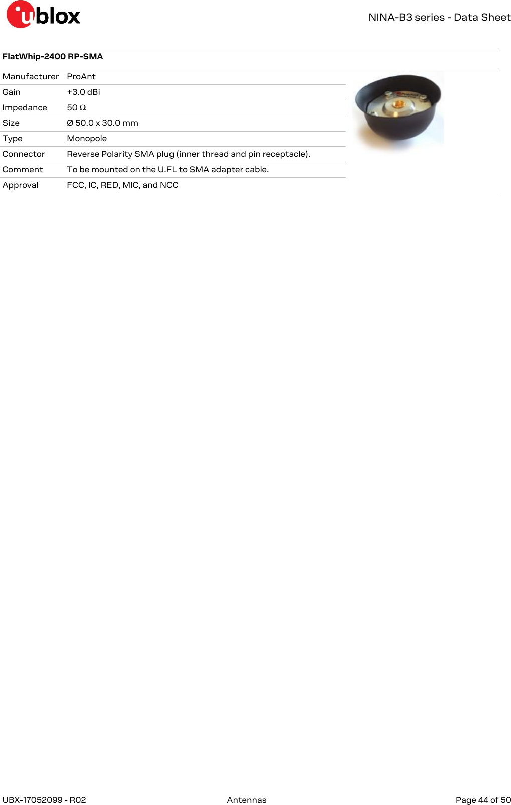
![NINA-B3 series - Data Sheet UBX-17052099 - R02 Antennas Page 43 of 50 Ex-IT 2400 RP-SMA 70-002 Manufacturer ProAnt Polarization Vertical Gain +3.0 dBi Impedance 50 Ω Size Ø 10 x 83 mm Type Monopole Connector Reverse Polarity SMA plug (inner thread and pin receptacle) Comment To be mounted on the U.FL to Reverse Polarity SMA adapter cable. An SMA version antenna is also available but not recommended for use (Ex-IT 2400 SMA 70-002). Approval FCC, IC, RED, MIC, and NCC InSide-2400 Manufacturer ProAnt Gain +3.0 dBi Impedance 50 Ω Size 27 x 12 mm (triangular) Type Patch Cable length 100 mm Connector U.FL. connector Comment Should be attached to a plastic enclosure or part for best performance. To be mounted on a U.FL connector. See the NINA-B3 series System Integration Manual [3] for information how to integrate the U.FL connector. It is required to follow this reference design to comply with the NINA-B3 FCC/IC modular approvals. Approval FCC, IC, RED, MIC, and NCC FlatWhip-2400 SMA Manufacturer ProAnt Gain +3.0 dBi Impedance 50 Ω Size Ø 50.0 x 30.0 mm Type Monopole Connector SMA plug (inner thread and pin) Comment To be mounted on the U.FL to SMA adapter cable. Approval RED, MIC, and NCC](https://usermanual.wiki/u-blox/NINAB31.user-manual/User-Guide-3999355-Page-43.png)
![NINA-B3 series - Data Sheet UBX-17052099 - R02 Product handling Page 45 of 50 8 Product handling 8.1 Packaging The NINA-B3 series modules are delivered as hermetically sealed, reeled tapes to enable efficient production, production lot set-up and tear-down. For more information about packaging, see the u-blox Package Information Guide [1]. 8.1.1 Reels The NINA-B3 modules are deliverable in quantities of 500 pieces on a reel. The reel types for the NINA-B3 modules are provided in Table 23 and detailed information about the reel types are described in the u-blox Package Information Guide [1]. Model Reel Type NINA-B3x1 B NINA-B3x2 A Table 23: Reel types for different models of the NINA-B3 series 8.1.2 Tapes TBD 8.2 Moisture sensitivity levels ⚠ The NINA-B3 series modules are Moisture Sensitive Devices (MSD) in accordance with the IPC/JEDEC specification. The Moisture Sensitivity Level (MSL) relates to the required packaging and handling precautions. The NINA-B3 series modules are rated at MSL level 4. For more information regarding moisture sensitivity levels, labeling and storage, see the u-blox Package Information Guide [1]. ☞ For MSL standards, see IPC/JEDEC J-STD-020, which can be downloaded from www.jedec.org. 8.3 Reflow soldering Reflow profiles are selected according to u-blox recommendations. See NINA-B3 series System Integration Manual [3] for more information. ⚠ Failure to observe these recommendations can result in severe damage to the device. 8.4 ESD precautions ⚠ The NINA-B3 series modules contain highly sensitive electronic circuitry and are Electrostatic Sensitive Devices (ESD). Handling the NINA-B3 series modules without proper ESD protection may destroy or damage them permanently. The NINA-B3 series modules are electrostatic sensitive devices (ESD) and require special ESD precautions typically applied to the ESD sensitive components. Section 4.1.1 provides the maximum ESD ratings of the NINA-B3 series modules. Proper ESD handling and packaging procedures must be applied throughout the processing, handling and operation of any application that incorporates the NINA-B3 series module. ⚠ Failure to observe these recommendations can result in severe damage to the device.](https://usermanual.wiki/u-blox/NINAB31.user-manual/User-Guide-3999355-Page-45.png)
![NINA-B3 series - Data Sheet UBX-17052099 - R02 Labeling and ordering information Page 47 of 50 Table 26 explains the parts of the product code. Code Meaning Example PPPP Form factor NINA TG Platform (Technology and Generation) T – Dominant technology, for example, W: Wi-Fi, B: Bluetooth G - Generation B3: Bluetooth Generation 3 VV Variant based on the same platform; range [00…99] 11: default configuration, with antenna pin TT Major product version 00: first revision Q Quality grade A: Automotive B: Professional C: Standard B: professional grade XX Minor product version (not relevant for certification) Default value is 00 Table 26: Part identification code 9.3 Ordering information Ordering Code Product NINA-B311-00B NINA-B3 module with antenna pin, pre-flashed and locked for use with u-blox connectivity software NINA-B312-00B NINA-B3 module with internal antenna, pre-flashed and locked for use with u-blox connectivity software NINA-B301-00B NINA-B3 module with antenna pin, open CPU for custom applications NINA-B302-00B NINA-B3 module with internal antenna, open CPU for custom applications Table 27: Product ordering codes](https://usermanual.wiki/u-blox/NINAB31.user-manual/User-Guide-3999355-Page-47.png)
![NINA-B3 series - Data Sheet UBX-17052099 - R02 Related documents Page 49 of 50 Related documents [1] u-blox Package Information Guide, document number UBX-14001652 [2] u-blox Short Range AT Commands Manual, document number UBX-14044127 [3] NINA-B3 Series System Integration Manual, document number UBX-15026175 [4] NINA-B3 Getting Started, document number UBX-18022394 ☞ For regular updates to u-blox documentation and to receive product change notifications, register on our homepage (www.u-blox.com). Revision history Revision Date Name Comments R01 10-Nov-2017 ajoh, apet, kgom Initial release. R02 10-Sep-2018 ajoh, kgom Removed Arm Mbed software option. Updated the mechanical specification (Section 5). Updated RF parameters such as output power and receiver sensitivity (Table 3). Added current consumption data when running the u-blox connectivity software (Table 14).](https://usermanual.wiki/u-blox/NINAB31.user-manual/User-Guide-3999355-Page-49.png)