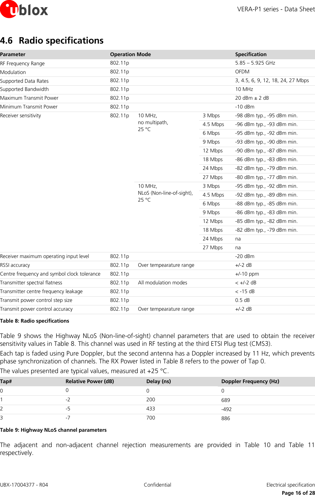
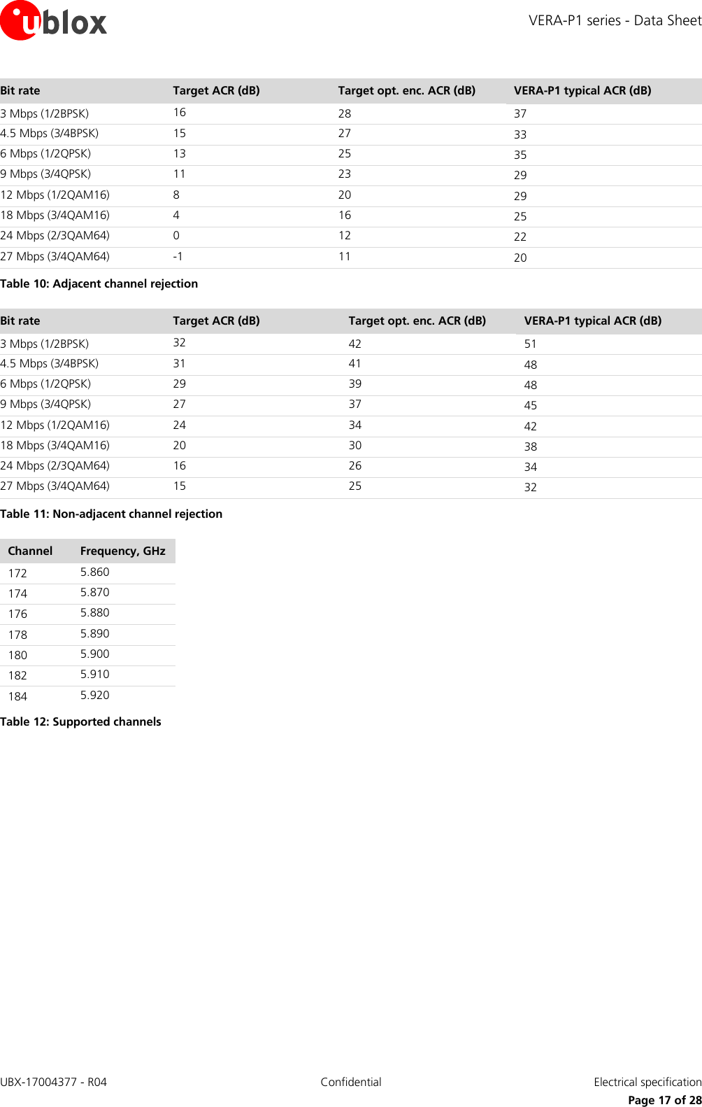
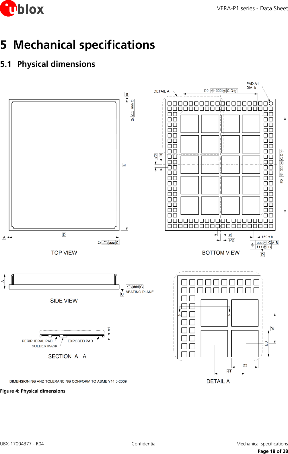
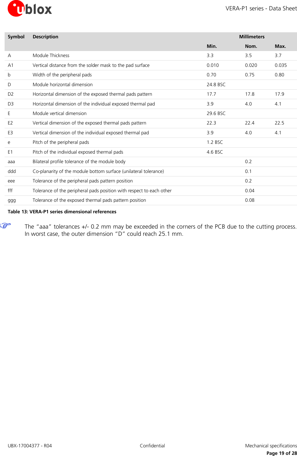
u blox VERAP173 IEEE 802.11p module for OBU units User Manual VERA P1 series

u-blox AG IEEE 802.11p module for OBU units VERA P1 series

User Manual

    VERA-P1 series Host-based V2X transceiver module Data Sheet                  Abstract This  technical  data  sheet  describes  the  VERA-P1  series  transceiver module  that  enables  development  of  electronics  for  Vehicle-to-Everything  (V2X)  communication  systems.  The  VERA-P1  series includes  an  integrated  MAC/LLC/Baseband  processor  and  the required  RF  front-end  components.  It  is  connected  to  a  host processor through a USB or SPI interface. www.u-blox.com UBX-17004377 - R04
VERA-P1 series - Data Sheet UBX-17004377 - R04 Confidential  Contents     Page 2 of 28 Document Information Title VERA-P1 series Subtitle Host-based V2X transceiver module Document type Data Sheet Document number UBX-17004377  Revision and date R04 7-Dec-2017 Disclosure restriction Confidential  Product Status  Corresponding content status  Functional Sample Draft For functional testing. Revised and supplementary data will be published later. In Development / Prototype Objective Specification Target values. Revised and supplementary data will be published later. Engineering Sample Advance Information Data based on early testing. Revised and supplementary data will be published later. Initial Production Early Prod. Information Data from product verification. Revised and supplementary data may be published later. Mass Production / End of Life Production Information Final product specification.  This document applies to the following products: Product name Type number Firmware version PCN reference Product Status VERA-P171 VERA-P171-00A-00 N/A N/A Prototype VERA-P173 VERA-P173-00A-00 N/A N/A Prototype VERA-P174 VERA-P174-00A-00 N/A N/A Prototype               u-blox reserves all rights to this document and the information contained herein. Products, names, logos and designs described herein may in whole or in part be subject to intellectual property rights. Reproduction, use, modification or disclosure to third parties of this document or any part thereof without the express permission of u-blox is strictly prohibited. The  information  contained herein  is  provided “as  is”  and u-blox  assumes no  liability for  the  use  of  the  information.  No warranty,  either express or implied, is given, including but not limited, with respect to the accuracy, correctness, reliability and fitness for a particular purpose of the information. This document may be revised by u-blox at any time. For most recent documents, visit www.u-blox.com.  Copyright © 2017, u-blox AG. u-blox is a registered trademark of u-blox Holding AG in the EU and other countries.
VERA-P1 series - Data Sheet UBX-17004377 - R04 Confidential  Contents     Page 3 of 28 Contents Contents .............................................................................................................................. 3 1 Functional description .................................................................................................. 5 1.1 Overview .............................................................................................................................................. 5 1.2 Product features ................................................................................................................................... 5 1.3 Block diagrams ..................................................................................................................................... 6 1.4 Product description ............................................................................................................................... 6 1.5 Supported features ............................................................................................................................... 7 2 Host interfaces ............................................................................................................. 8 2.1 USB interface ........................................................................................................................................ 8 2.2 SPI interface .......................................................................................................................................... 8 3 Pin Definition ................................................................................................................ 9 3.1 Pin description ...................................................................................................................................... 9 4 Electrical specification ................................................................................................ 14 4.1 Absolute maximum ratings ................................................................................................................. 14 4.2 Operating conditions .......................................................................................................................... 14 4.3 Digital pad ratings .............................................................................................................................. 14 4.4 Peak current consumption .................................................................................................................. 15 4.5 Current consumption.......................................................................................................................... 15 4.6 Radio specifications ............................................................................................................................ 16 5 Mechanical specifications .......................................................................................... 18 5.1 Physical dimensions ............................................................................................................................ 18 6 Qualification and approvals ...................................................................................... 20 6.1 Approvals ........................................................................................................................................... 20 6.1.1 European Union regulatory compliance ....................................................................................... 20 6.1.2 FCC compliance .......................................................................................................................... 20 6.1.3 IC compliance.............................................................................................................................. 20 6.1.4 FCC and IC IDs ............................................................................................................................ 20 6.1.5 Certification in other countries .................................................................................................... 21 7 Product handling & soldering .................................................................................... 22 7.1 Packaging ........................................................................................................................................... 22 7.1.1 Reels ........................................................................................................................................... 22 7.1.2 Tapes .......................................................................................................................................... 22 7.2 Shipment, storage and handling ......................................................................................................... 22 7.2.1 Moisture sensitivity levels ............................................................................................................. 22 7.2.2 Mounting process and soldering recommendations ..................................................................... 23 7.2.3 ESD handling precautions ............................................................................................................ 24
VERA-P1 series - Data Sheet UBX-17004377 - R04 Confidential  Contents     Page 4 of 28 8 Labeling and ordering information ........................................................................... 25 8.1 Product labeling .................................................................................................................................. 25 8.2 Explanation of codes........................................................................................................................... 25 8.3 Ordering codes ................................................................................................................................... 25 Appendix .......................................................................................................................... 26 Glossary ............................................................................................................................ 26 Related documents........................................................................................................... 27 Revision history ................................................................................................................ 27 Contact .............................................................................................................................. 28
VERA-P1 series - Data Sheet UBX-17004377 - R04 Confidential  Functional description     Page 5 of 28 1 Functional description 1.1 Overview The  VERA-P1  series  are  compact,  embedded  transceiver  modules  that  enables  development  of  electronics  for Vehicle-to-Everything  (V2X)  communication  systems.  These  automotive  grade  modules  are  designed  for applications such as traffic safety, intelligent traffic management and entertainment. The modules can be used for in-vehicle units (OBU - On Board Unit) – their use in V2X infrastructure (RSU - Road Side Unit) is intended, but not authorized yet. The VERA-P1 series modules provide superior performance compared to V2X systems based on consumer-grade Wi-Fi chipsets, especially at high vehicle speeds and in non-line-of-sight (NLOS) conditions. The  VERA-P1  series  includes  an  integrated  MAC/LLC/Baseband  processor  and  the  required  RF  front-end components. The module is connected to a host processor through USB or SPI interface. Both interfaces can be used for data communication and firmware download. 1.2 Product features  Table 1: VERA-P1 series main features summary
VERA-P1 series - Data Sheet UBX-17004377 - R04 Confidential  Functional description     Page 6 of 28 1.3 Block diagrams  Figure 1: Block diagram of VERA-P171  Figure 2: Block diagram of VERA-P173 and VERA-P174  1.4 Product description Model Description VERA-P171 Single channel, no antenna diversity, one antenna VERA-P173 Single channel, antenna diversity, two antennas VERA-P174 Dual channel or single channel with antenna diversity, two antennas Table 2: Product description
VERA-P1 series - Data Sheet UBX-17004377 - R04 Confidential  Functional description     Page 7 of 28 1.5 Supported features  Compliance with WAVE and ETSI ITS G5 for US and Europe operations  USB and SPI1 host interfaces  Frequency band 5.850 – 5.925 MHz (channels 172, 174, 176, 178, 180, 182, 184)  Channel bandwidth 10 MHz2  Data rates 3, 4.5, 6, 9, 12, 18, 24, 27 Mbps  Antenna diversity (VERA-P173, VERA-P174) – CDD for TX and MRC for RX mode  TX output power from -10 to +23 dBm (Class C), RX sensitivity -97 dBm at 3 Mbps  Power supply 3.3 V and 5.0 V, 4 W maximum  Operation temperature -40 °C to +95 °C  Dimensions 29.6 x 24.8 x 3.5 mm                                                        1 SPI is not recommended as the main host interface for communication due to performance limitations. 2 Support for 20 MHz mode is planned for future firmware releases subject to certain limitations, as the requirements for 20 MHz operation have not been fully specified.
VERA-P1 series - Data Sheet UBX-17004377 - R04 Confidential  Host interfaces     Page 8 of 28 2 Host interfaces 2.1 USB interface The  VERA-P1  series  module  supports  a USB  2.0  high-speed  interface  for  firmware  loading  (booting)  and  high speed data transfer (> 200 Mbps). The USB interface of the module is powered with 3.3 V supply voltage. The module acts as a device on the USB bus. 2.2 SPI interface The VERA-P1 series module supports an SPI interface for firmware loading (booting) and data communication. Firmware can be loaded by the host processor while the module operates as a slave or from the FLASH memory while the module is in the master mode. When the module is configured as a master, it needs a USB interface connection for communication to the host. The interface is capable of full-duplex operation in  master or slave mode. The maximum clock rate is 50 MHz in master mode, and 25 MHz in slave mode3.                                                          3 SPI host interface for data communication in slave mode is tested only with 15 MHz clock rate.
VERA-P1 series - Data Sheet UBX-17004377 - R04 Confidential  Pin Definition     Page 9 of 28 3 Pin Definition 3.1 Pin description  Figure 3: Pin allocation (top view)
VERA-P1 series - Data Sheet UBX-17004377 - R04 Confidential  Pin Definition     Page 10 of 28 No. Name Pin type Power domain Description A1 GND Ground - Ground A2 GND Ground - Ground A3 RSTn I VIO Module Reset, has internal pull-up 100k to VIO A4 GND Ground - Ground A5 3V3 Power - Baseband/Radio supply (3.0 to 3.6V) A6 GND Ground - Ground A7 NC - - Leave unconnected A8 VIO Power - I/O voltage (1.8/2.5/3.3V), in case of 1.8V pin 8 can get supply from pin B7 A9 GND Ground - Ground A10 NC - - Leave unconnected   A11 GND Ground - Ground A12 NC - - Leave unconnected A13 NC - - Leave unconnected A14 NC - - Leave unconnected A15 NC - - Leave unconnected A16 NC - - Leave unconnected A17 NC - - Leave unconnected A18 GND Ground - Ground A19 5V0_A1 Power - Antenna 1 radio front-end supply (4.5 to 5.5V) A20 GND Ground - Ground A21 NC - - Leave unconnected A22 NC - - Leave unconnected A23 GND Ground - Ground A24 GND Ground - Ground A25 GND Ground - Ground A26 ANT1 RF I/O - Antenna 1 A27 GND Ground - Ground A28 GND Ground - Ground A29 NC - - Leave unconnected A30 GND Ground - Ground A31 GND Ground - Ground A32 NC - - Leave unconnected A33 GND Ground - Ground A34 GND Ground - Ground A35 NC - - Leave unconnected A36 GND Ground - Ground A37 GND Ground - Ground A38 NC - - Leave unconnected A39 GND Ground - Ground A40 GND Ground - Ground A41 ANT2 RF I/O - Antenna 2 A42 GND Ground - Ground A43 GND Ground - Ground A44 GND Ground - Ground
VERA-P1 series - Data Sheet UBX-17004377 - R04 Confidential  Pin Definition     Page 11 of 28 No. Name Pin type Power domain Description A45 5V0_A2 Power - Antenna 2 radio front-end supply (4.5 to 5.5 V) A46 GND Ground - Ground A47 SPI_MOSI I/O VIO SPI Bus A48 SPI_MISO I/O VIO SPI Bus A49 MOD_IO_SPARE I/O VIO Optional SPI CS A50 GND Ground - Ground A51 NC - - Leave unconnected A52 NC - - Leave unconnected A53 NC - - Leave unconnected A54 NC - - Leave unconnected A55 NC - - Leave unconnected A56 NC - - Leave unconnected A57 GND Ground - Ground A58 NC - - Leave unconnected A59 NC - - Leave unconnected A60 NC - - Leave unconnected A61 GND Ground - Ground A62 USB_DN I/O - USB Bus A63 USB_DP I/O - USB Bus A64 USB_VBUS I - USB VBUS detect input A65 GND Ground - Ground A66 GND Ground - Ground A67 GND Ground - Ground A68 NC - - Leave unconnected A69 GND Ground - Ground A70 1PPS I 1V8 One pulse per second input A71 GND Ground - Ground A72 NC - - Leave unconnected A73 NC - - Leave unconnected A74 NC - - Leave unconnected A75 NC - - Leave unconnected A76 NC - - Leave unconnected A77 GND Ground - Ground A78 NC - - Leave unconnected A79 BOOT_0 I VIO Boot mode configuration A80 NC - - Leave unconnected A81 GND Ground - Ground A82 NC - - Leave unconnected A83 NC - - Leave unconnected A84 GND Ground - Ground B1 NC - - Leave unconnected B2 NC - - Leave unconnected B3 GND Ground - Ground B4 3V3 Power - Baseband/Radio supply (3.0 to 3.6 V) B5 GND Ground - Ground
VERA-P1 series - Data Sheet UBX-17004377 - R04 Confidential  Pin Definition     Page 12 of 28 No. Name Pin type Power domain Description B6 NC - - Leave unconnected B7 1V8 O - 1.8 V supply output, can be connected to pin 8 only as a VIO voltage source B8 GND Ground - Ground B9 NC - - Leave unconnected B10 GND Ground - Ground B11 NC - - Leave unconnected B12 NC - - Leave unconnected B13 NC - - Leave unconnected B14 NC - - Leave unconnected B15 NC - - Leave unconnected B16 NC - - Leave unconnected B17 GND Ground - Ground B18 5V0_A1 Power - Antenna 1 radio front-end supply (4.5 to 5.5 V) B19 GND Ground - Ground B20 NC - - Leave unconnected B21 NC - - Leave unconnected B22 GND Ground - Ground B23 GND Ground - Ground B24 GND Ground - Ground B25 NC - - Leave unconnected B26 NC - - Leave unconnected B27 NC - - Leave unconnected B28 GND Ground - Ground B29 GND Ground - Ground B30 GND Ground - Ground B31 GND Ground - Ground B32 GND Ground - Ground B33 GND Ground - Ground B34 NC - - Leave unconnected B35 NC - - Leave unconnected B36 NC - - Leave unconnected B37 GND Ground - Ground B38 GND Ground - Ground B39 GND Ground - Ground B40 5V0_A2 Power - Antenna 2 radio front-end supply (4.5 to 5.5 V) B41 GND Ground - Ground B42 SPI_SCK I/O VIO SPI Bus B43 SPI_CSn I/O VIO SPI Bus B44 NC - - Leave unconnected B45 GND Ground - Ground B46 NC - - Leave unconnected B47 NC - - Leave unconnected B48 NC - - Leave unconnected B49 NC - - Leave unconnected B50 NC - - Leave unconnected
VERA-P1 series - Data Sheet UBX-17004377 - R04 Confidential  Pin Definition     Page 13 of 28 No. Name Pin type Power domain Description B51 NC - - Leave unconnected B52 GND Ground - Ground B53 NC - - Leave unconnected B54 NC - - Leave unconnected B55 NC - - Leave unconnected B56 GND Ground - Ground B57 NC - - Leave unconnected B58 NC - - Leave unconnected B59 NC - - Leave unconnected B60 NC - - Leave unconnected B61 NC - - Leave unconnected B62 NC - - Leave unconnected B63 GND Ground - Ground B64 NC - - Leave unconnected B65 NC - - Leave unconnected B66 NC - - Leave unconnected B67 NC - - Leave unconnected B68 NC - - Leave unconnected B69 NC - - Leave unconnected B70 GND Ground - Ground B71 BOOT_2 I VIO Boot mode configuration B72 BOOT_1 I VIO Boot mode configuration B73 NC - - Leave unconnected B74 GND Ground - Ground B75 NC - - Leave unconnected B76 NC - - Leave unconnected EP GND Ground - 20 Ground/Thermal exposed pads, connect to the ground Table 3: VERA-P1 series pin description
VERA-P1 series - Data Sheet UBX-17004377 - R04 Confidential  Electrical specification     Page 14 of 28 4 Electrical specification  Stressing the device above one or more of the ratings listed in the Absolute Maximum Rating section may cause permanent damage. These are stress  ratings only. Operating the module at these or at any conditions other than those specified in the Operating conditions section of this document  should  be  avoided.  Exposure  to  absolute  maximum  rating  conditions  for  extended periods may affect device reliability.  Operating condition ranges define those limits within which the functionality of the device is guaranteed. Where application information is given, it is advisory only and does not form part of the specification. 4.1 Absolute maximum ratings Symbol Description Min.  Max. Units 5V0_A1, 5V0_A2 Power supply voltage 5.0 V -0.3 6.0 V 3V3 Power supply voltage 3.3 V -0.3 3.9 V VIO I/O supply voltage 1.8 V/2.5 V/3.3 V -0.3 3.9 V TSTORAGE Storage temperature -40 +95 ºC Table 4: Absolute maximum ratings  The  product  is  not  protected  against  overvoltage  or  reversed  voltages.  If  necessary,  voltage spikes exceeding the power supply voltage specification, given in table above, must be limited to values within the specified boundaries by using appropriate protection devices. 4.2 Operating conditions Symbol Parameter Min.  Typ Max. Units 5V0_A1, 5V0_A2 Power supply voltage 5.0 V 4.5 5.0 5.5 V 3V3 Power supply voltage 3.3 V 3.0 3.3 3.6 V VIO I/O supply voltage 1.8 V/2.5 V/3.3 V 1.65 1.8 1.95  V 2.3 2.5 2.8  3.0 3.3 3.6 V TA Ambient operating temperature -40 - +95 ºC Ripple Noise Peak-to-peak voltage ripple on 5V0 and 3V3 supply lines. - - 10 mV Table 5: Operating conditions 4.3 Digital pad ratings Symbol Parameter Conditions Min. Max. Units VIH Input high voltage  0.7*VIO4 VIO1 V VIL Input low voltage  -0.3 0.65 V VHYS Input hysteresis  0.18 - V VOH Output high voltage IOmax = 5 mA VIO-0.4 - V VOH Output low voltage IOmax = -5 mA - 0.4 V Table 6: Digital pad ratings                                                       4 1PPS pad always use 1.8 V internally generated IO supply regardless of the VIO pad voltage. 5 RSTn pad internally pulled high to VIO voltage by 100k. During reset it should be below 0.2 V.
VERA-P1 series - Data Sheet UBX-17004377 - R04 Confidential  Electrical specification     Page 15 of 28 4.4 Peak current consumption Operation Mode Peak current6 (mA) 3V3 VIO7 5V0_A1 5V0_A2 RX  700 TBD  35 35 TX  +23 dBm 700 TBD  500 500 +15 dBm 700 TBD  TBD TBD +10 dBm 700 TBD  TBD TBD +0 dBm 700 TBD  TBD TBD Table 7: Peak current consumption 4.5 Current consumption Power consumption for different operation modes – TBD                                                        6 Peak values are shown. The average current for full operation mode strongly depends on RX/TX time ratio and remains within the range between the peak values of RX and TX. 7 VIO current is shown for 1.8 V I/O voltage.
VERA-P1 series - Data Sheet UBX-17004377 - R04 Confidential  Electrical specification     Page 16 of 28 4.6 Radio specifications Parameter Operation Mode Specification RF Frequency Range  802.11p   5.85 – 5.925 GHz Modulation  802.11p   OFDM Supported Data Rates  802.11p   3, 4.5, 6, 9, 12, 18, 24, 27 Mbps Supported Bandwidth  802.11p  10 MHz Maximum Transmit Power  802.11p  20 dBm ± 2 dB Minimum Transmit Power  802.11p  -10 dBm Receiver sensitivity  802.11p 10 MHz,  no multipath, 25 °C 3 Mbps -98 dBm typ., -95 dBm min. 4.5 Mbps -96 dBm typ., -93 dBm min. 6 Mbps -95 dBm typ., -92 dBm min. 9 Mbps -93 dBm typ., -90 dBm min. 12 Mbps -90 dBm typ., -87 dBm min. 18 Mbps -86 dBm typ., -83 dBm min. 24 Mbps -82 dBm typ., -79 dBm min. 27 Mbps -80 dBm typ., -77 dBm min. 10 MHz, NLoS (Non-line-of-sight), 25 °C 3 Mbps -95 dBm typ., -92 dBm min. 4.5 Mbps -92 dBm typ., -89 dBm min. 6 Mbps -88 dBm typ., -85 dBm min. 9 Mbps -86 dBm typ., -83 dBm min. 12 Mbps -85 dBm typ., -82 dBm min. 18 Mbps -82 dBm typ., -79 dBm min. 24 Mbps na 27 Mbps na Receiver maximum operating input level 802.11p   -20 dBm RSSI accuracy 802.11p Over tempearature range  +/-2 dB Centre frequency and symbol clock tolerance 802.11p   +/-10 ppm Transmitter spectral flatness 802.11p All modulation modes  < +/-2 dB Transmitter centre frequency leakage  802.11p   < -15 dB Transmit power control step size  802.11p   0.5 dB Transmit power control accuracy  802.11p Over tempearature range  +/-2 dB Table 8: Radio specifications Table  9  shows  the  Highway  NLoS  (Non-line-of-sight)  channel  parameters  that  are  used  to  obtain  the  receiver sensitivity values in Table 8. This channel was used in RF testing at the third ETSI Plug test (CMS3). Each tap is faded using Pure Doppler, but the second antenna has a Doppler increased by 11 Hz, which prevents phase synchronization of channels. The RX Power listed in Table 8 refers to the power of Tap 0. The values presented are typical values, measured at +25 °C. Tap# Relative Power (dB) Delay (ns) Doppler Frequency (Hz) 0 0 0 0 1 -2 200 689 2 -5 433 -492 3 -7 700 886 Table 9: Highway NLoS channel parameters The  adjacent  and  non-adjacent  channel  rejection  measurements  are  provided  in  Table  10  and  Table  11 respectively.
VERA-P1 series - Data Sheet UBX-17004377 - R04 Confidential  Electrical specification     Page 17 of 28 Bit rate Target ACR (dB) Target opt. enc. ACR (dB) VERA-P1 typical ACR (dB) 3 Mbps (1/2BPSK) 16 28 37 4.5 Mbps (3/4BPSK) 15 27 33 6 Mbps (1/2QPSK) 13 25 35 9 Mbps (3/4QPSK) 11 23 29 12 Mbps (1/2QAM16) 8 20 29 18 Mbps (3/4QAM16) 4 16 25 24 Mbps (2/3QAM64) 0 12 22 27 Mbps (3/4QAM64) -1 11 20 Table 10: Adjacent channel rejection Bit rate Target ACR (dB) Target opt. enc. ACR (dB) VERA-P1 typical ACR (dB) 3 Mbps (1/2BPSK) 32 42 51 4.5 Mbps (3/4BPSK) 31 41 48 6 Mbps (1/2QPSK) 29 39 48 9 Mbps (3/4QPSK) 27 37 45 12 Mbps (1/2QAM16) 24 34 42 18 Mbps (3/4QAM16) 20 30 38 24 Mbps (2/3QAM64) 16 26 34 27 Mbps (3/4QAM64) 15 25 32 Table 11: Non-adjacent channel rejection Channel Frequency, GHz 172 5.860 174 5.870 176 5.880 178 5.890 180 5.900 182 5.910 184 5.920 Table 12: Supported channels
VERA-P1 series - Data Sheet UBX-17004377 - R04 Confidential  Mechanical specifications     Page 18 of 28 5 Mechanical specifications 5.1 Physical dimensions   Figure 4: Physical dimensions
VERA-P1 series - Data Sheet UBX-17004377 - R04 Confidential  Mechanical specifications     Page 19 of 28 Symbol Description Millimeters   Min. Nom. Max. A  Module Thickness 3.3 3.5 3.7 A1 Vertical distance from the solder mask to the pad surface 0.010 0.020 0.035 b Width of the peripheral pads 0.70 0.75 0.80 D Module horizontal dimension 24.8 BSC D2 Horizontal dimension of the exposed thermal pads pattern 17.7 17.8 17.9 D3 Horizontal dimension of the individual exposed thermal pad 3.9 4.0 4.1 E Module vertical dimension  29.6 BSC E2 Vertical dimension of the exposed thermal pads pattern 22.3 22.4 22.5 E3 Vertical dimension of the individual exposed thermal pad 3.9 4.0 4.1 e Pitch of the peripheral pads 1.2 BSC E1 Pitch of the individual exposed thermal pads 4.6 BSC aaa Bilateral profile tolerance of the module body  0.2  ddd Co-planarity of the module bottom surface (unilateral tolerance)  0.1  eee Tolerance of the peripheral pads pattern position  0.2  fff Tolerance of the peripheral pads position with respect to each other  0.04  ggg Tolerance of the exposed thermal pads pattern position  0.08  Table 13: VERA-P1 series dimensional references  The “aaa” tolerances +/- 0.2 mm may be exceeded in the corners of the PCB due to the cutting process. In worst case, the outer dimension “D” could reach 25.1 mm.
VERA-P1 series - Data Sheet UBX-17004377 - R04 Confidential  Qualification and approvals     Page 20 of 28 6 Qualification and approvals 6.1 Approvals8  Products  marked  with  this  lead-free  symbol  on  the  product  label  comply  with  the "Directive 2002/95/EC of the European Parliament and the Council on the Restriction of Use of certain Hazardous Substances in Electrical and Electronic Equipment" (RoHS). VERA-P1 series V2X modules are RoHS compliant. 6.1.1 European Union regulatory compliance TBD 6.1.2 FCC compliance The VERA-P173 module complies with Part 95, Subpart L of the FCC Rules. Operation is subject to the following two conditions: 1. This device may not cause harmful interference, and 2. This  device  must  accept  any  interference  received,  including  interference  that  may  cause  undesired operation. Non authorized modification could void authority to use this equipment. The internal / external antenna(s) used for  this  module  must  provide  a  separation  distance  of  at  least  20  cm  from  all  persons  and  must  not  be  co-located or operating in conjunction with any other antenna or transmitter. These  limits  are  designed  to  provide  reasonable  protection  against  harmful  interference  in  a  residential installation.  This  equipment  generates,  uses  and  can  radiate  radio  frequency  energy  and,  if  not  installed  and used  in  accordance  with  the  manufacturer’s  instructions,  may  cause  harmful  interference  to  radio communications.  The outside of final product that contains the VERA-P173 module must display in a user accessible area a label  referring  to  the  enclosed  module.  This  exterior  label  can  use  wording  such  as  the  following: “Contains Transmitter Module FCC ID: XPYVERAP173”  or “Contains FCC ID: XPYVERAP173”.  Part 95, Subpart L covers DSRC service of On-Board Units. VERA-P173 authorization for Road Side Units is pending.  6.1.3 IC compliance TBD 6.1.4 FCC and IC IDs Model FCC ID IC ID VERA-P171 tbd tbd VERA-P173 XPYVERAP173 tbd VERA-P174 tbd tbd Table 14: FCC and IC IDs for different models of VERA-P1 series                                                       8 These approvals are pending.
VERA-P1 series - Data Sheet UBX-17004377 - R04 Confidential  Qualification and approvals     Page 21 of 28 6.1.5 Certification in other countries TBD 6.2 Approved antennas VERA-P173 is certified to be used with dipole antennas of up to 6 dBi peak gain. Table 15 below lists an example of an approved antenna. Model name Manufacturer and description Gain [dBi] (peak) TD.10.5113 Taoglas, Dipole Terminal Antenna SMA Connector 5.88 dBi Table 15: Approved antennas (example)
VERA-P1 series - Data Sheet UBX-17004377 - R04 Confidential  Product handling & soldering     Page 22 of 28 7 Product handling & soldering 7.1 Packaging The  VERA-P1  series  modules  are  delivered  as  hermetically  sealed,  reeled  tapes  to  enable  efficient  production, production  lot  set-up  and  tear-down.  For  more  information  about  packaging,  see  the  u-blox  Package Information Guide [1]. 7.1.1 Reels The VERA-P1 series modules are deliverable in quantities of  250 pieces on a reel.  The VERA-P1 series modules are shipped on reel Type A as specified in the u-blox Package Information Guide [1].  7.1.2 Tapes The dimensions of the tapes are specified in Figure 5.  Figure 5: VERA-P1 tape dimensions 7.2 Shipment, storage and handling  For more information regarding shipment, storage and handling see the u-blox Package Information Guide [1]. 7.2.1 Moisture sensitivity levels  The  VERA-P1  series  modules  are  rated  at  moisture  sensitivity  level  3.  See  moisture  sensitive  warning  label  on each shipping bag for detailed information. After opening the dry pack, modules must be mounted within 168 hours in factory conditions of maximum 30 °C/60%RH or must be stored at less than 10%RH. Modules require baking  if  the  humidity  indicator  card  shows  more  than  10%  when  read  at  23±5°C  or  if  the  conditions mentioned above are not met. Please refer to J-STD-033B standard for bake procedure.
VERA-P1 series - Data Sheet UBX-17004377 - R04 Confidential  Product handling & soldering     Page 23 of 28 7.2.2 Mounting process and soldering recommendations The  VERA-P1  series module  is a  surface mount  module  supplied  on an  8-layer FR4-type PCB  with gold plated connection pins and produced in a lead-free process with a lead-free soldering paste. The wrap page of the PCB is  max.  0,75%  according  to  IPC-A-610E.  The  thickness  of  solder  resist  on  the  host  PCB  top  side  and  the JODY-W1 bottom side must be considered for the soldering process. This module is compatible with industrial reflow profile for RoHS/Pb-free solders, Sn96.5/Ag3.0/Cu0.5 solder is a right choice.  Use of  "No Clean"  soldering paste  is strongly recommended, cleaning  the  populated  modules  is strongly discouraged - residuals under the module cannot be easily removed with any cleaning process. Cleaning with  water  can  lead  to  capillary  effects  where  water  is  absorbed  into  the  gap  between  the  host  board  and module. The combination of soldering flux residuals and encapsulated water could lead to short circuits between neighboring pins. Only a single reflow soldering process is permitted for host boards with the VERA-P1 series modules. The reflow profile used is dependent on the thermal mass of the entire populated PCB, heat transfer efficiency of the oven and particular type of solder paste used. Since the profile used is process and layout dependent, the optimum profile should be studied case by case. Recommendations below should be taken as a starting point guide. In case of basic information necessity, refer to J-STD-020C standard.  Profile feature Sn-Pb eutectic (Sn63/Pb37) RoHS/Pb-free (Sn96.5/Ag3.0/Cu0.5) Ramp up rate (TSMAX to TP) 3 °C/sec max 3 °C/sec max Minimum soak temperature (TSMIN) 100 °C 150 °C Maximum soak temperature (TSMAX) 150 °C 200 °C Soak time (ts) 60 - 120 sec 60 - 180 sec Liquidus temperature (TL) 183 °C 217 °C Time above TL  (tL) 60 - 150 sec 60 - 150 sec Peak temperature (TP) 215 – 225 °C 235 – 245 °C Time within +0 / -5°C of actual TP (tp) 10 - 30 sec 20 - 40 sec Ramp down rate 6 °C/sec max 6 °C/sec max Time from 25°C to TP 6 min max 8 min max Table 16: Recommended reflow profile  The lowest value of TP  and slower ramp down rate (2 – 3 °C/sec) is preferred.  Figure 6: Reflow profile
VERA-P1 series - Data Sheet UBX-17004377 - R04 Confidential  Product handling & soldering     Page 24 of 28 7.2.3 ESD handling precautions  VERA-P1  series  modules  are  Electrostatic  Sensitive  Devices  (ESD).  Observe  precautions  for handling! Failure to observe these precautions can result in severe damage to the Wi-Fi receiver! Wi-Fi  transceivers  are  Electrostatic  Sensitive  Devices  (ESD)  and  require  special  precautions  when  handling. Particular  care  must  be  exercised  when  handling  patch  antennas,  due  to  the  risk  of  electrostatic  charges.  In addition  to  standard  ESD  safety  practices,  the  following  measures  should  be  taken  into  account  whenever handling the receiver:  Unless there is a galvanic coupling between the local GND (i.e. the work table) and the PCB GND, then the first point of contact when handling the PCB must always be between the local GND and PCB GND.  Before mounting an antenna patch, connect ground of the device   When handling the RF pin, do not come into contact with any charged capacitors and be careful when contacting materials that can develop charges (e.g. patch antenna ~10 pF, coax cable ~50-80 pF/m, soldering iron, …)   To prevent electrostatic discharge through the RF input, do not touch any exposed antenna area. If there is any risk that such exposed antenna area is touched in non ESD protected work area, implement proper ESD protection measures in the design.   When soldering RF connectors and patch antennas to the receiver’s RF pin, make sure to use an ESD safe soldering iron (tip).
VERA-P1 series - Data Sheet UBX-17004377 - R04 Confidential  Labeling and ordering information     Page 25 of 28 8 Labeling and ordering information 8.1 Product labeling 8.2 Explanation of codes Three different product code formats are used. The  Product Name is used in documentation such as this data sheet  and  identifies  all  u-blox  products,  independent  of  packaging  and  quality  grade.  The  Ordering  Code includes options and  quality, while the  Type Number  includes the hardware and firmware  versions. Table  17 below details these three different formats: Format Structure Product Name PPPP-TGVV Ordering Code PPPP-TGVV-TTQ Type Number PPPP-TGVV-TTQ-XX Table 17: Product Code Formats Code Meaning Example PPPP Form factor VERA TG Platform T – Dominant technology, For example, W: Wi-Fi, B: Bluetooth G - Generation P1 VV Variant based on the same platform; range [00…99] 71 TT Major Product Version 00 Q Quality grade A: Automotive B: Professional C: Standard A XX Minor product version (not relevant for certification) 00 Table 18: Part identification code 8.3 Ordering codes Ordering Code Product name Product VERA-P171-00A-00 VERA-P171 VERA-P171 automotive grade module VERA-P173-00A-00 VERA-P173 VERA-P173 automotive grade module VERA-P174-00A-00 VERA-P174 VERA-P174 automotive grade module EVK-VERA-P174-00A EVK-VERA-P174 VERA-P171/3/4 Evaluation kit Table 19: Product ordering codes  Product changes affecting form, fit or function are documented by u-blox. For a list of Product Change Notifications (PCNs) see our website.
VERA-P1 series - Data Sheet UBX-17004377 - R04 Confidential  Appendix     Page 26 of 28 Appendix Glossary Name Definition COTS Commercial off-the-shelf CS Chip select  ESD Electrostatic Sensitive Devices ETSI European Telecommunications Standards Institute FCC Federal Communications Commission  GND Ground GPIO General-purpose input/output IC Industry Canada  LLC Logical Link Control MAC Media Access Control nACR Non-adjacent channel rejection  NLoS Non-Line-of-Sight OBU On Board Unit OFDM Orthogonal frequency-division multiplexing  PCB Printed Circuit Board RF Radio Frequency RSU Road Side Unit RoHS Restriction of Hazardous Substances SPI Serial Peripheral Interface USB Universal Serial Bus V2X Vehicle-to-Everything Table 20: Explanation of abbreviations used
VERA-P1 series - Data Sheet UBX-17004377 - R04 Confidential  Related documents     Page 27 of 28 Related documents [1] u-blox Package Information Guide, document number UBX-14001652    For regular updates to u-blox documentation and to receive product change notifications, register on our homepage (http://www.u-blox.com). Revision history  Revision Date Name Comments R01 23-Feb-2017 ishe, kgom Initial release. R02 5-May-2017 ddie, kgom Added VERA-P174 product variant and included block diagram, FCC/IC ID, and ordering code for this variant. R03 11-Sep-2017 mzes, kgom, ddie Updated Table 1. Included footnotes in section 1.5. Updated the ordering codes (section 8.3). Added reel size (section 7.1) and tape dimensions (Figure 5).  R04 7-Dec-2017 ddie, kgom Removed  references to  VERA-P175 variant.  Updated  Table  1.  Added  section  6.1.2  on  FCC compliance. Removed watermark. Clarified that RSU operation is not approved (Section 1.1). Updated maximum transmit power (Section 4.6).
VERA-P1 series - Data Sheet UBX-17004377 - R04 Confidential  Contact     Page 28 of 28 Contact For complete contact information visit us at www.u-blox.com. u-blox Offices     North, Central and South America u-blox America, Inc. Phone:  +1 703 483 3180 E-mail:  info_us@u-blox.com  Regional Office West Coast: Phone:  +1 408 573 3640 E-mail:  info_us@u-blox.com Technical Support: Phone:  +1 703 483 3185 E-mail:  .support@u-blox.com  Headquarters Europe, Middle East, Africa u-blox AG  Phone:  +41 44 722 74 44 E-mail:  info@u-blox.com  Support:  support@u-blox.com Documentation Feedback  E-mail:  docsupport@u-blox.com   Asia, Australia, Pacific u-blox Singapore Pte. Ltd. Phone:  +65 6734 3811 E-mail:  info_ap@u-blox.com Support:  support_ap@u-blox.com  Regional Office Australia: Phone:  +61 2 8448 2016 E-mail:  info_anz@u-blox.com Support:  support_ap@u-blox.com Regional Office China (Beijing): Phone:  +86 10 68 133 545 E-mail:  info_cn@u-blox.com  Support:  support_cn@u-blox.com Regional Office China (Chongqing): Phone:  +86 23 6815 1588 E-mail:  info_cn@u-blox.com  Support:  support_cn@u-blox.com Regional Office China (Shanghai): Phone:  +86 21 6090 4832 E-mail:  info_cn@u-blox.com  Support:  support_cn@u-blox.com Regional Office China (Shenzhen): Phone:  +86 755 8627 1083 E-mail:  info_cn@u-blox.com  Support:  support_cn@u-blox.com Regional Office India: Phone:  +91 80 4050 9200 E-mail:  info_in@u-blox.com  Support:  support_in@u-blox.com  Regional Office Japan (Osaka): Phone:  +81 6 6941 3660 E-mail:  info_jp@u-blox.com  Support:  support_jp@u-blox.com  Regional Office Japan (Tokyo): Phone:  +81 3 5775 3850 E-mail:  info_jp@u-blox.com  Support:  support_jp@u-blox.com  Regional Office Korea: Phone:  +82 2 542 0861 E-mail:  info_kr@u-blox.com  Support:  support_kr@u-blox.com Regional Office Taiwan: Phone:  +886 2 2657 1090 E-mail:  info_tw@u-blox.com  Support:  support_tw@u-blox.com

Navigation menu