u blox WIBEAR11N-SF2 WLAN & Bluetooth Module User Manual ELLA W1 Antenna TraceDesigns UBX 16016269

u-blox AG WLAN & Bluetooth Module ELLA W1 Antenna TraceDesigns UBX 16016269
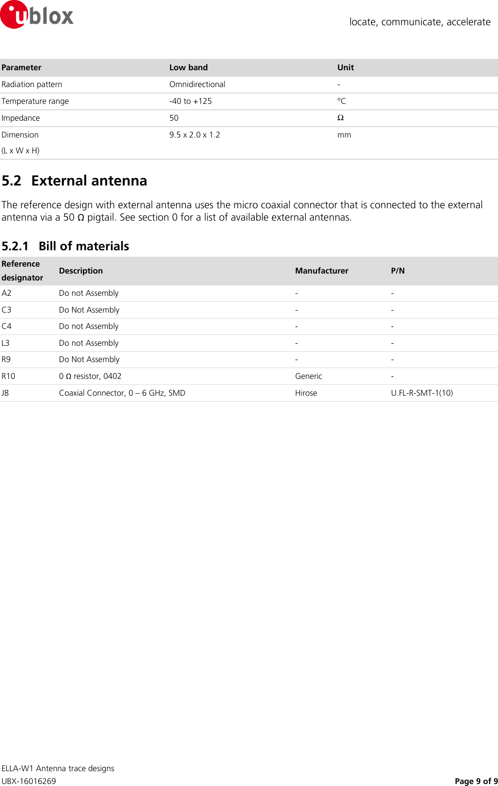
Contents

ELLA-W1_Antenna TraceDesigns_(UBX-16016269)

 ELLA-W1 Antenna trace designs     UBX-16016269    Page 1 of 9  locate, communicate, accelerate ELLA-W1 Antenna trace designs Topic : ELLA-W1 Antenna trace designs Doc.No: UBX-16016269  Revision R02  Date:  Name Signature Created 01-Jul-2016 Stefano Bianconi sbia Checked 01-Jul-2016 Igor Shevchenko ishe Released 06-Jul-2016 Daniel Dietterle ddie We reserve all rights in this document and in the information contained therein. Reproduction, use or disclosure to third parties without express authority is strictly forbidden.   © 2016 u-blox AG 1 Scope This  document  defines  the  essential  specifications  necessary  to  implement  the  ELLA-W1  antenna  reference designs. The information contained herein and its references should be sufficient to guide a skilled person in an attempt  to  implement  the  design  on  a  host  carrier.  It  will  provide  the  designer  with  PCB  layout  details  and expected performance specifications. The document supports the four different PCB designs:   Two connector-based designs for the use of external antennas (one for each antenna pin of the module)   Two designs based on SMD antennas (one for each antenna pin of the module) 2 FCC/IC ID reference Model1 FCC ID IC ID ELLA-W131 PV7-WIBEAR11N-SF1 7738A-WB11NSF1 ELLA-W133 PV7-WIBEAR11N-SF2 7738A-WB11NSF2 ELLA-W161 PV7-WIBEAR11N-DF1 7738A-WB11NDF1 ELLA-W163 PV7-WIBEAR11N-DF2 7738A-WB11NDF2 Table 1: FCC and IC IDs for different models of ELLA-W1 series                                                       1 The FCC and IC IDs are the same for professional and automotive grade variants of each ELLA-W1 model.
 ELLA-W1 Antenna trace designs     UBX-16016269    Page 2 of 9  locate, communicate, accelerate 3 General description When using the ELLA-W1 together with this antenna reference design, the circuit trace layout must be made in strict compliance with the instructions below. All the components placed on each RF trace must be kept as indicated in the reference design, even if not used. The PCB areas of unused reference designs must be flooded with ground.  Figure 1: Antenna Reference design embedded in a host carrier PCB Reference Description 1 Host carrier PCB (light green) 2 Antenna reference design (dark green)  1 2
 ELLA-W1 Antenna trace designs     UBX-16016269    Page 3 of 9  locate, communicate, accelerate 3.1 Floor plan and PCB stack-up This section describes where the critical components are positioned on the reference design. It also presents the stack-up of the four layers of the PCB.   Figure 2: ELLA-W1 antenna reference design Reference Description 3 SMD antenna 4 Antenna impedance matching network 5 Connectors for external antenna  6 Antenna coplanar microstrip, matched to 50 Ω 7 Top layer GND-plane 8 Antenna impedance matching network 9 SMD antenna 10 ELLA-W1 module   3 6 10 4 5 9 7 8
 ELLA-W1 Antenna trace designs     UBX-16016269    Page 4 of 9  locate, communicate, accelerate 3.2 PCB stack-up The stack-up used in the reference design is specified in Table 2. PCB Layer Material Thickness Soldermask Top Generic LPI Soldermask 25 µm Top Copper Foil 35 µm Dielectric Pre-preg 2x7628 360 µm L2 Copper Foil 35 µm Dielectric Core 700  µm +/-10% L3 Copper Foil 35 µm Dielectric Pre-preg 2x7628 360 µm Bottom Copper Foil 35 µm Soldermask Bottom Generic LPI Soldermask 25 µm Table 2: Stack-up of EVK-ELLA-W1 3.2.1 RF trace specification The 50 Ω coplanar micro-strip dimensions used in these reference designs are stated in Figure 2 and Table 3.  Figure 3: Coplanar micro-strip dimension specification Item Value S 400 µm W 600 µm T 35 µm H 360 µm Table 3: Coplanar micro-strip specification
 ELLA-W1 Antenna trace designs     UBX-16016269    Page 5 of 9  locate, communicate, accelerate 3.3 Mechanical dimensions The mechanical dimensions and position of the components are specified in Figure 3.  The layers beneath the ‘top layer’ have the same dimensions and are filled with ground. No RF traces are routed in those layers.  Figure 4: Mechanical dimensions of EVK-ELLA-W1, top layer
 ELLA-W1 Antenna trace designs     UBX-16016269    Page 6 of 9  locate, communicate, accelerate 4 Reference designs for antenna pin 1 This section describes the available designs for the antenna pin 1 of the ELLA-W1 modules.  Figure 5: Reference schematic for antenna pin 1 4.1 Internal antenna The reference design with internal antenna uses the SMD Antenova type A10194 dual-band antenna that is connected to the module RF-port via a coplanar micro-strip transmission line. 4.1.1 Bill of materials Reference designator Description Manufacturer P/N A1 Antenna CHIP 2.45 & 5 GHz Antenova A10194 L1 IND, Multilayer Ceramic, 10nH, +/-5%, 300mA, SMD 0402 Johanson Technology L-07C10NJV6ST L2 IND, Multilayer Ceramic, 1nH, +/-0.3nH, 300mA, SMD 0402 Johanson Technology L-07C1N0SV6T C2 CAP, CER, 0.2pF, +/-0.1pF, C0G, 50V, SMD 0402 Johanson Technology 500R07S0R2BV4 R1 0 Ω resistor, 0402 Generic - R2 Do not Assembly - - J7 Do Not Assembly - - 4.1.2 Antenna characteristics Parameter Low band High band Unit Frequency Range 2.4 – 2.5  4.9 – 5.875  GHz Peak Gain 1.8 4.1 dBi VSWR < 1.4:1 < 1.8:1 - Efficiency >75 >60 % Polarisation Linear - Radiation pattern Omnidirectional - Temperature range -40  to +85 °C Impedance 50 Ω Dimension (L x W x H) 10.0 x 10.0 x 0.9 mm
 ELLA-W1 Antenna trace designs     UBX-16016269    Page 7 of 9  locate, communicate, accelerate 4.2 External antenna The reference design with external antenna uses the micro coaxial connector that is connected to the external antenna via a 50 Ω pigtail. See section 0 for a list of available external antennas. 4.2.1 Bill of materials Reference designator Description Manufacturer P/N A1 Do Not Assembly - - L1 Do Not Assembly - - L2 Do Not Assembly - - C2 Do Not Assembly - - R1 Do Not Assembly - - R2 0 Ω resistor, 0402 Generic - J7 Coaxial Connector, 0 – 6 GHz, SMD Hirose U.FL-R-SMT-1(10)
 ELLA-W1 Antenna trace designs     UBX-16016269    Page 8 of 9  locate, communicate, accelerate 5 Reference designs for antenna pin 2 This section describes the available designs for the antenna pin 2 of the ELLA-W1 modules. Note that only ELLA-W133 and ELLA-W163 use antenna pin 2, for Bluetooth transmission.  Figure 6: Reference schematic for antenna pin 2 5.1 Internal antenna The reference design with internal antenna uses the SMD Johanson Technology type 2450AT45A100 antenna that is connected to the module RF-port via a coplanar micro-strip transmission line.  5.1.1 Bill of materials Reference designator Description Manufacturer P/N A2 Antenna CHIP 2.4-2.5GHz Johanson Technology 2450AT45A100 C3 CAP, CER, 2.2pF, +/-0.1pF, C0G, 50V, SMD 0402 Johanson Technology 500R07S2R2BV4 C4 CAP, CER, 1.8pF, +/-0.1pF, C0G, 50V, SMD 0402 Johanson Technology 500R07S1R8BV4 L3 IND, Multilayer Ceramic, 3.9nH, +/-0.3nH, 300mA, SMD 0402 Johanson Technology L-07C3N9SV6T R9 0 Ω resistor, 0402 Generic - R10 Do not Assembly - - J8 Do Not Assembly - - 5.1.2 Antenna characteristics Parameter Low band Unit Frequency Range 2.4 – 2.5  GHz Peak Gain 2.2 dBi VSWR < 2:1 - Polarisation Linear -
 ELLA-W1 Antenna trace designs     UBX-16016269    Page 9 of 9  locate, communicate, accelerate Parameter Low band Unit Radiation pattern Omnidirectional - Temperature range -40 to +125  °C Impedance 50 Ω Dimension (L x W x H) 9.5 x 2.0 x 1.2 mm 5.2 External antenna The reference design with external antenna uses the micro coaxial connector that is connected to the external antenna via a 50 Ω pigtail. See section 0 for a list of available external antennas. 5.2.1 Bill of materials Reference designator Description Manufacturer P/N A2 Do not Assembly - - C3 Do Not Assembly - - C4 Do not Assembly - - L3 Do not Assembly - - R9 Do Not Assembly - - R10 0 Ω resistor, 0402 Generic - J8 Coaxial Connector, 0 – 6 GHz, SMD Hirose U.FL-R-SMT-1(10)

Navigation menu