Telit Communications S p A LE940B6NA LE940B6-NA User Manual
Telit Communications S.p.A. LE940B6-NA
UserManual.wiki
>
Telit Communications S p A
>
LE940B6NA User Manual
User Manual
Navigation menu
Upload a User Manual
Namespaces
Wiki Guide
HTML
PDF
Info
Views
User Manual
Discussion / Help
Navigation

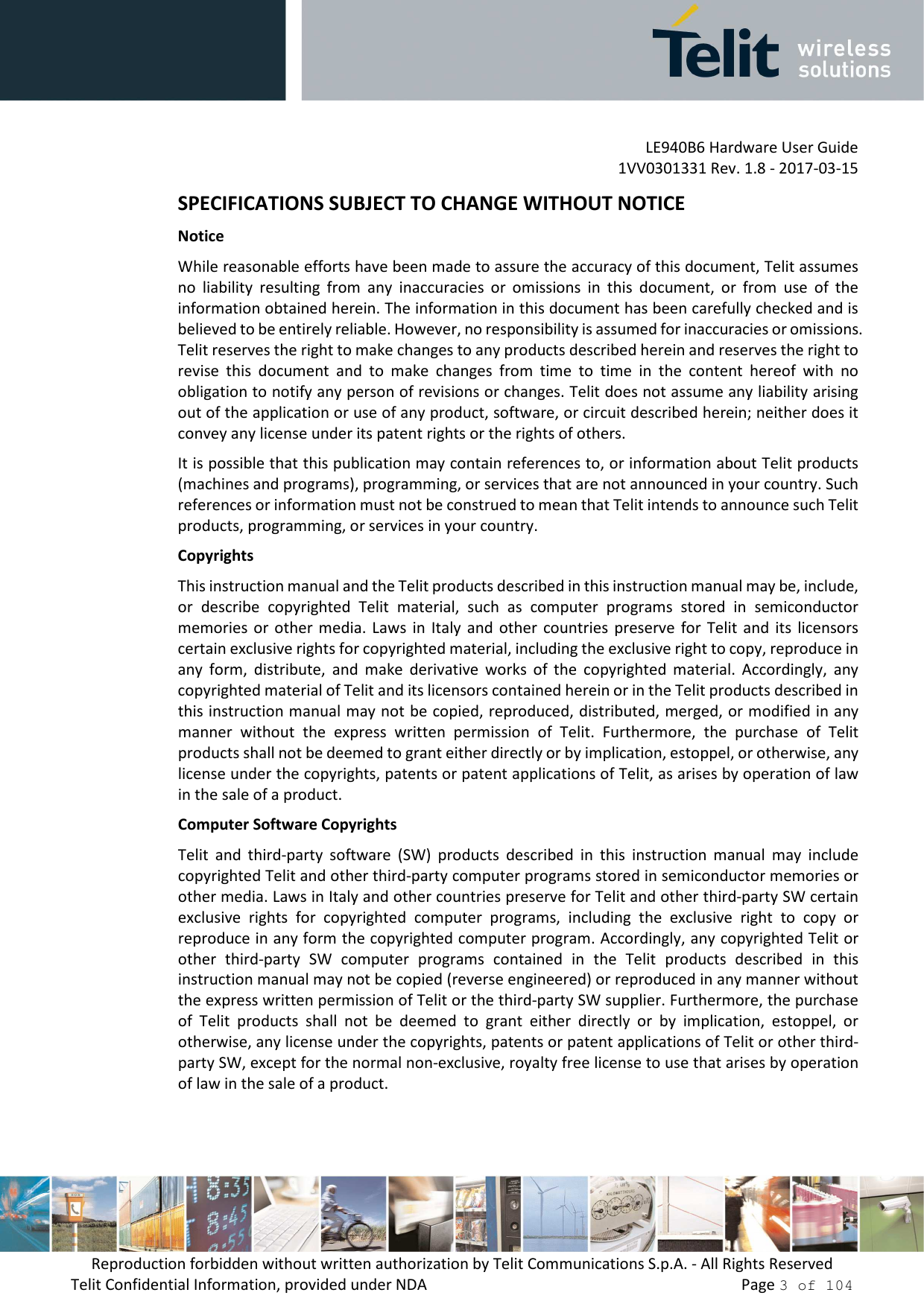


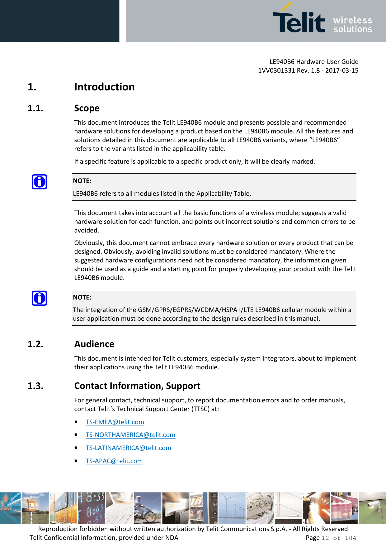
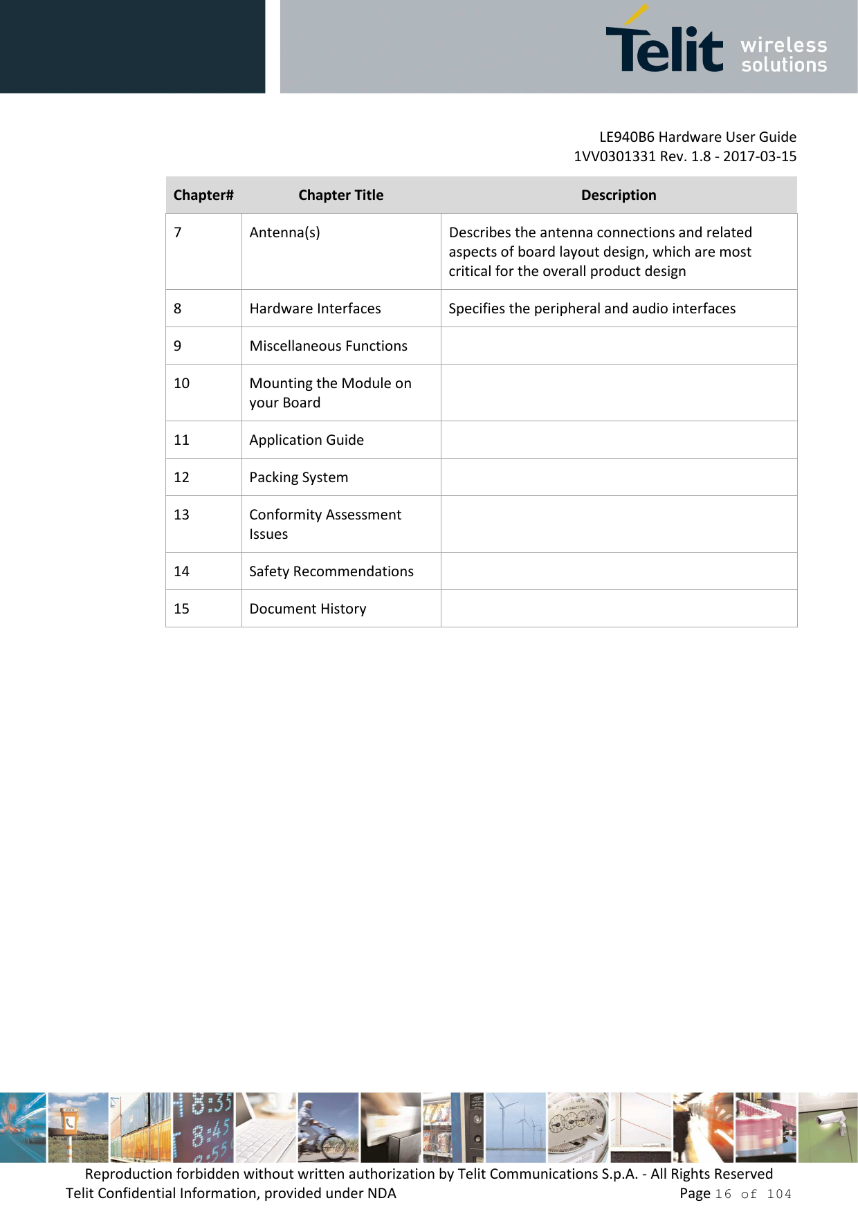

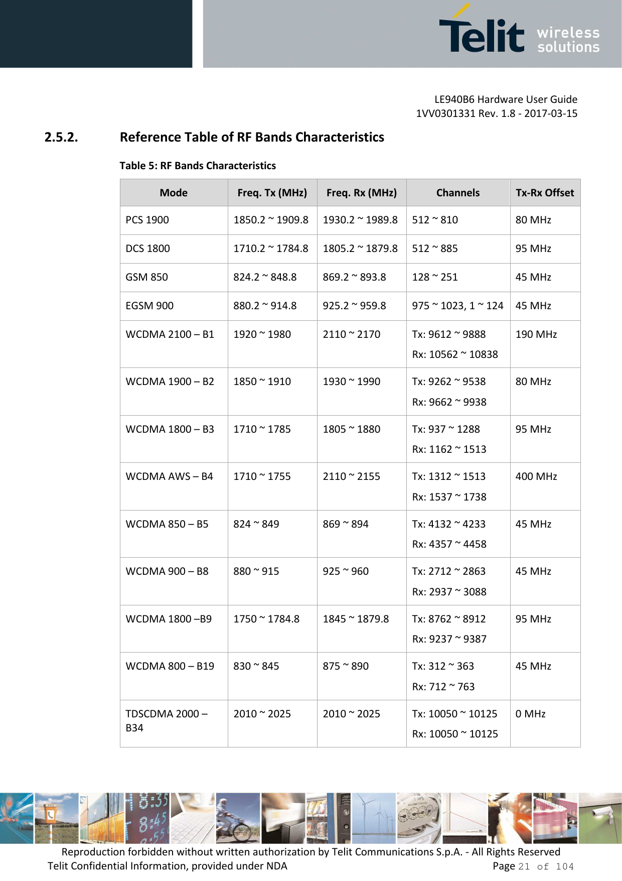


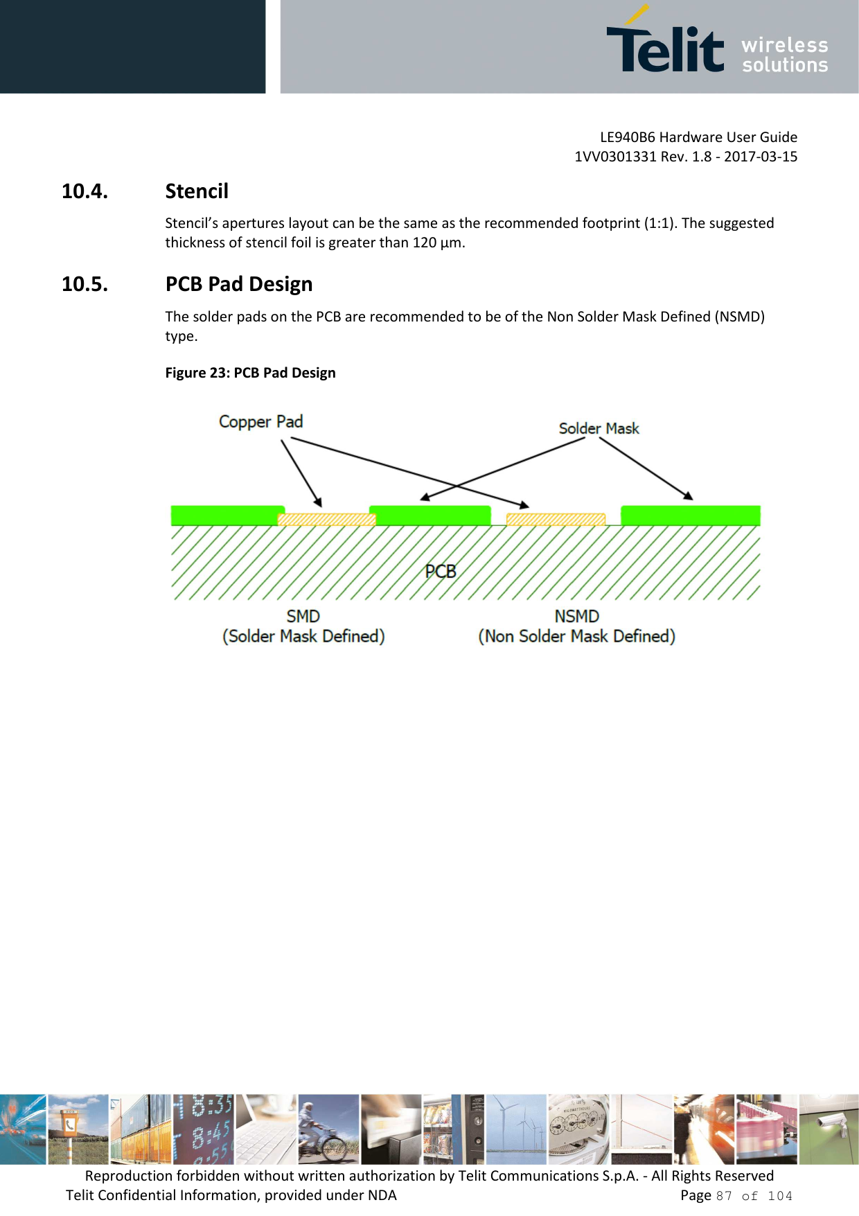
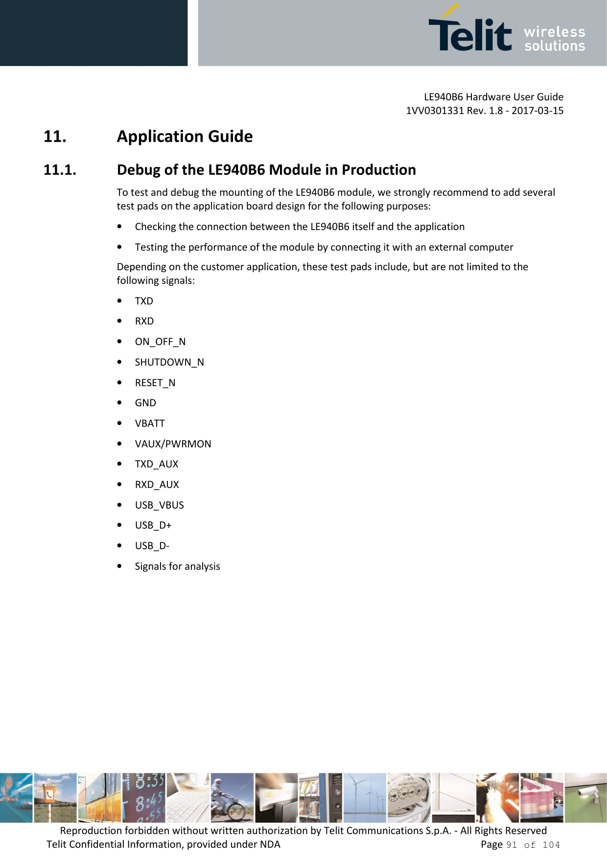
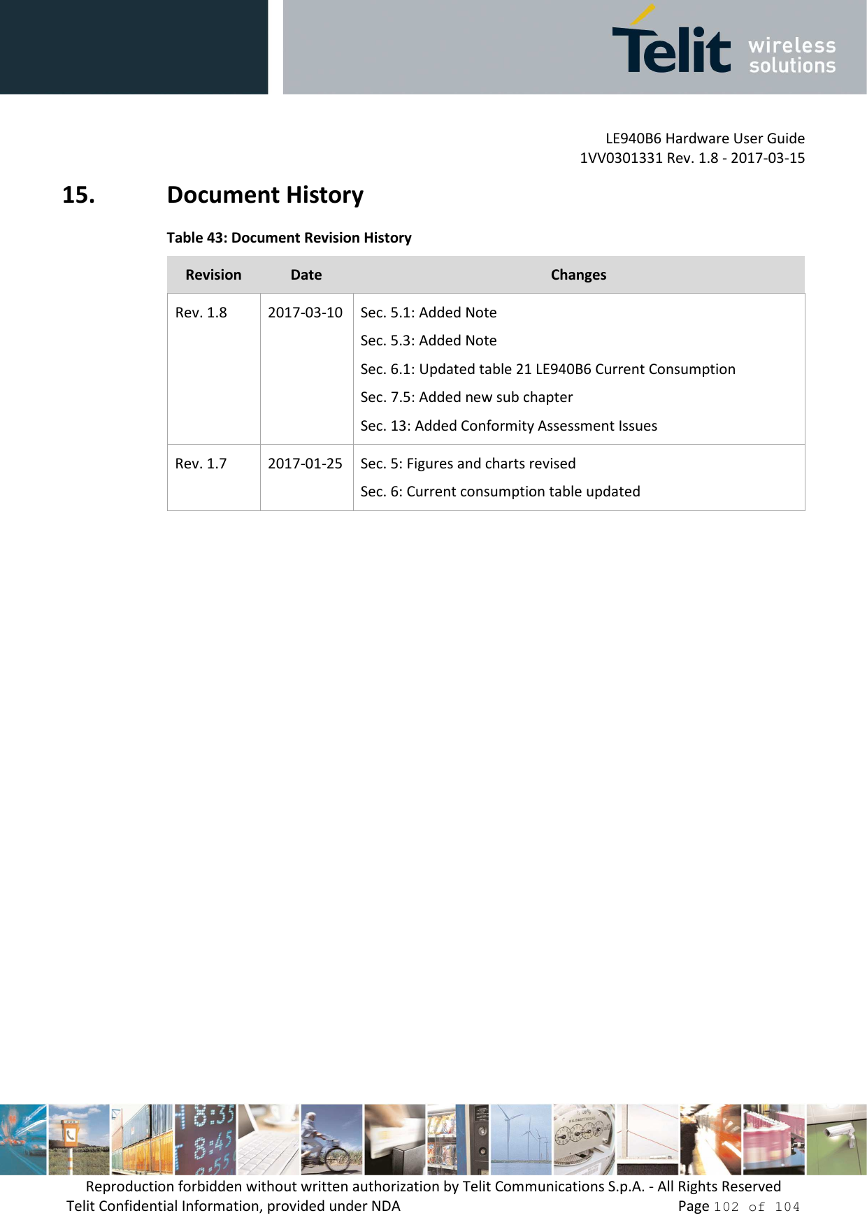
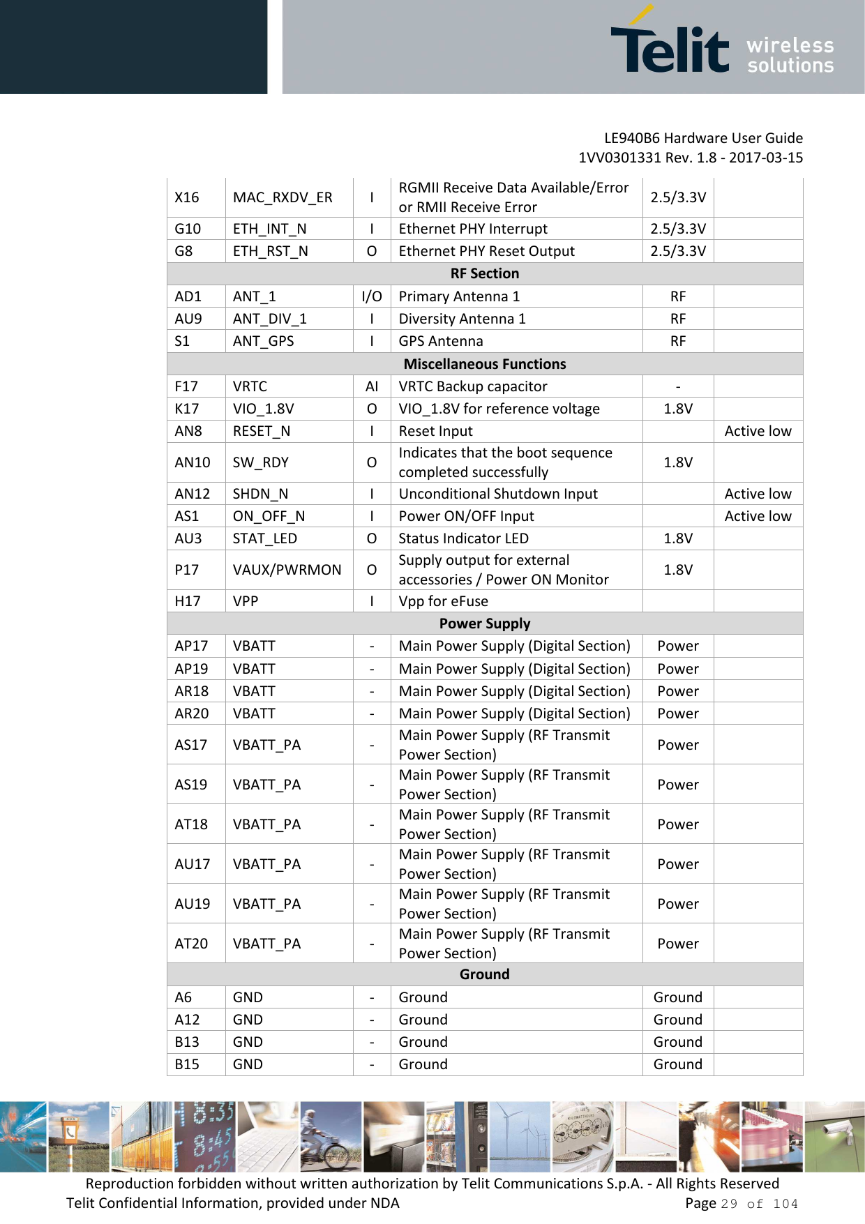
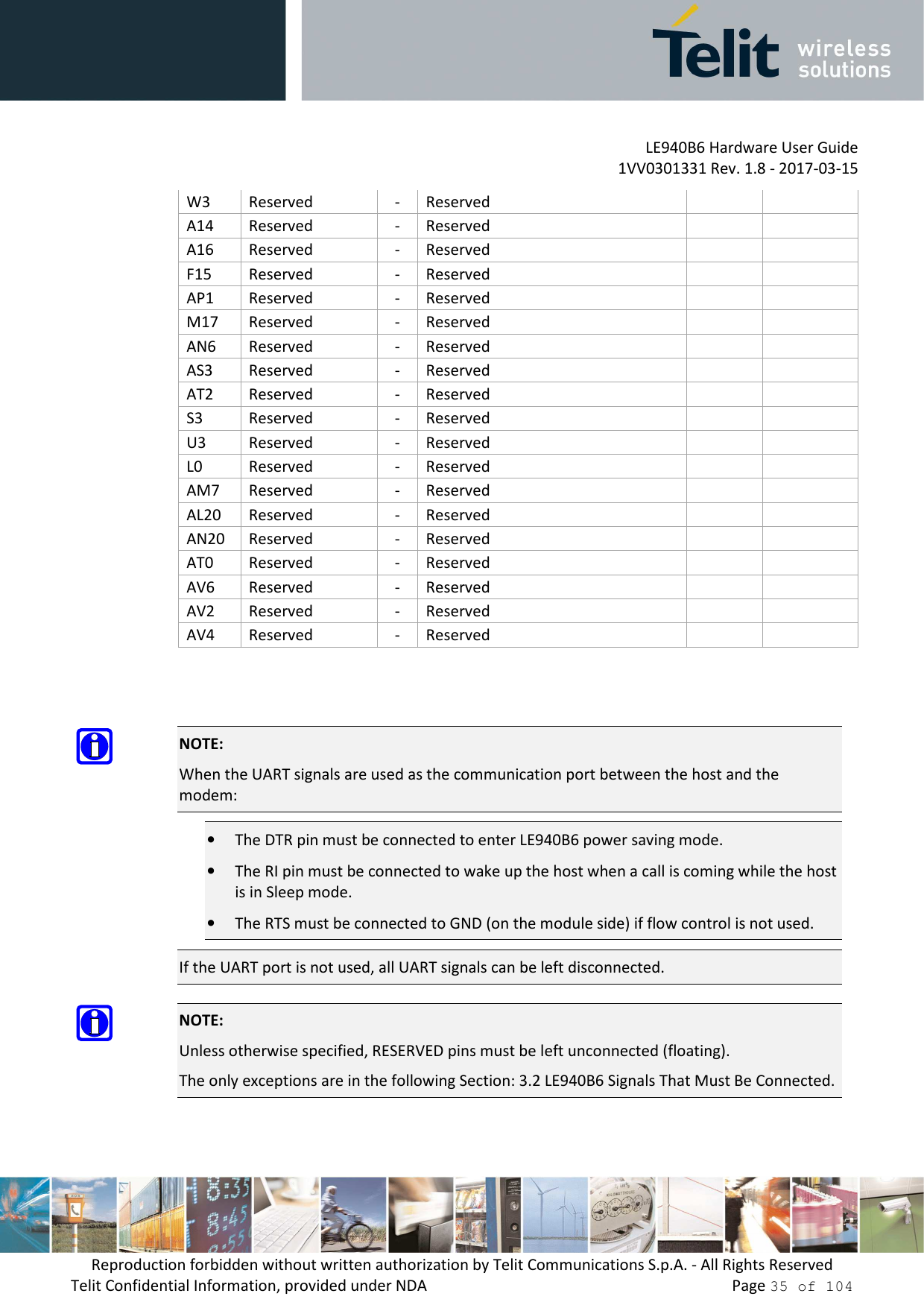
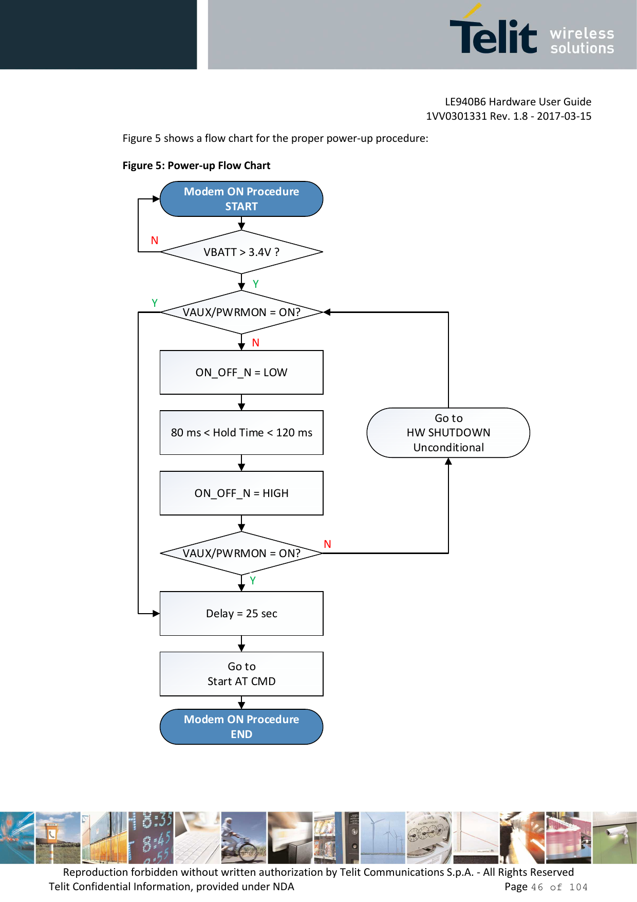
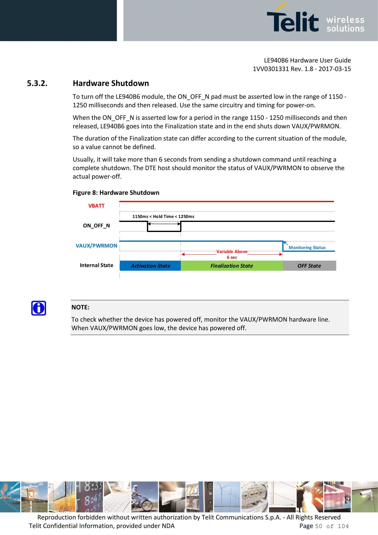
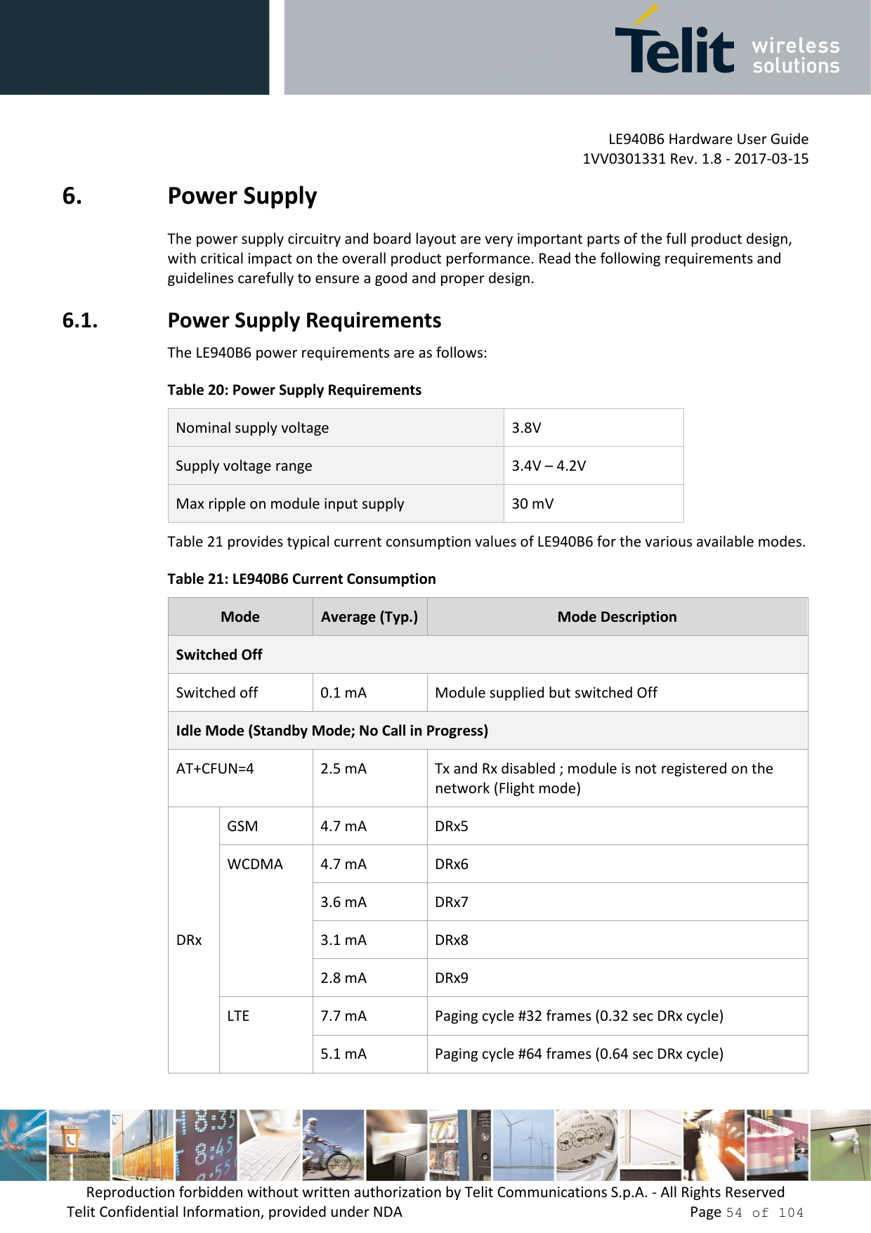
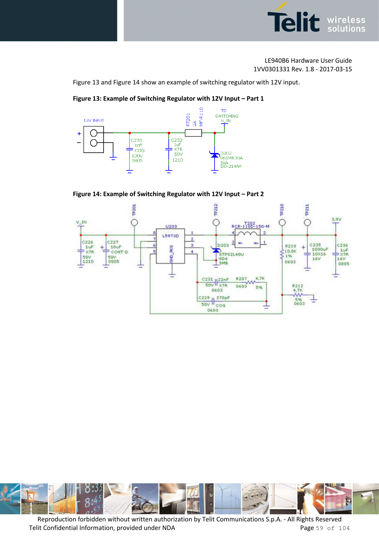
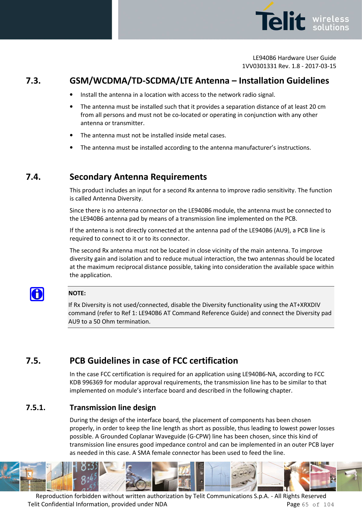
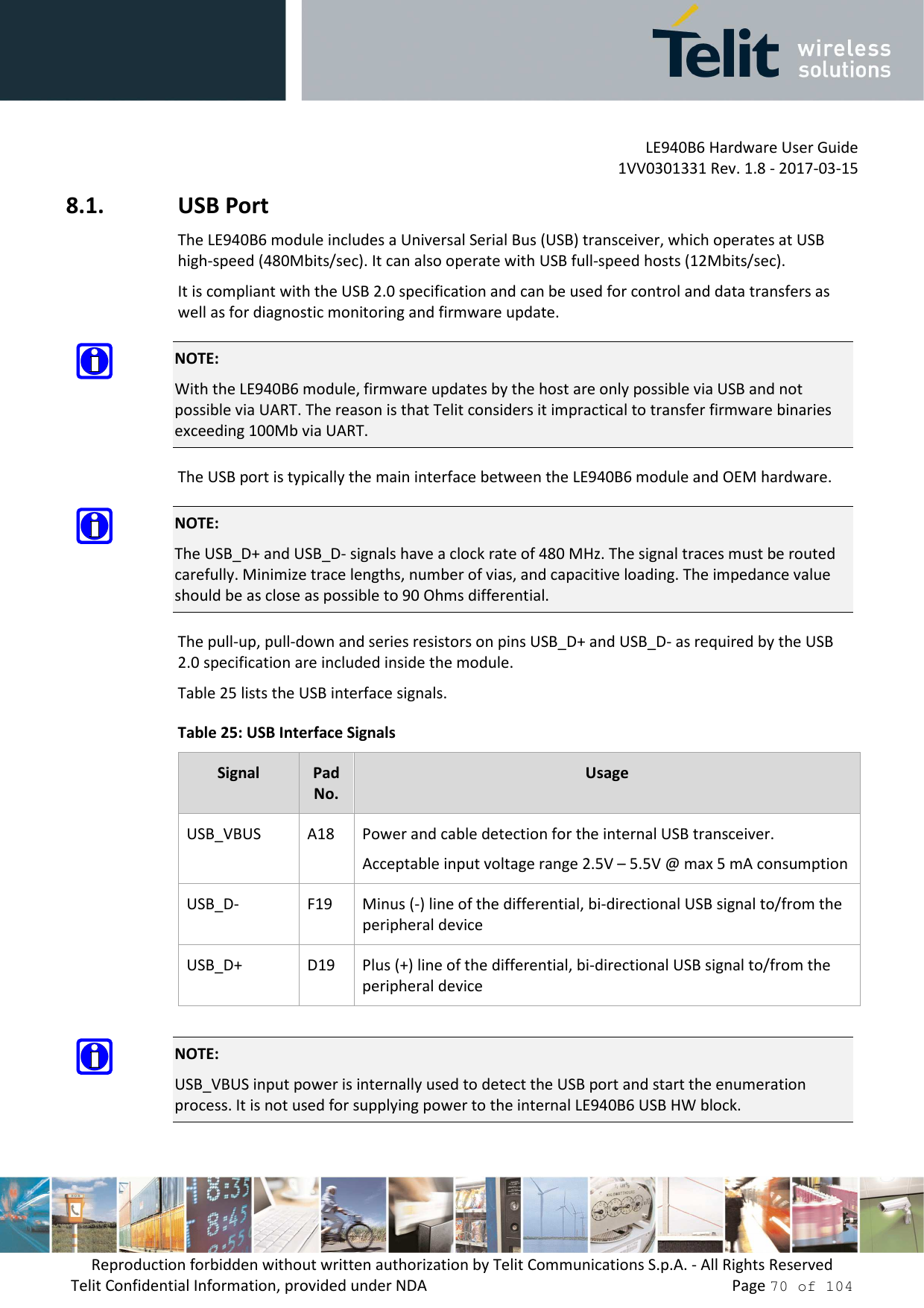
![LE940B6 Hardware User Guide 1VV0301331 Rev. 1.8 - 2017-03-15 Reproduction forbidden without written authorization by Telit Communications S.p.A. - All Rights Reserved Telit Confidential Information, provided under NDA Page 28 of 104 N18 SPI_CS O SPI Chip select output 1.8V P19 SPI_CLK O SPI Clock output 1.8V I2C Interface C14 I2C_SCL I/O I2C Clock 1.8V D13 I2C_SDA I/O I2C Data 1.8V Digital I/O F9 GPIO_01 I/O GPIO_01 1.8V E10 GPIO_02 I/O GPIO_02 1.8V F11 GPIO_03 I/O GPIO_03 1.8V E12 GPIO_04 I/O GPIO_04 1.8V F13 GPIO_05 I/O GPIO_05 1.8V E14 GPIO_06 I/O GPIO_06 1.8V R18 GPIO_07 I/O GPIO_07 1.8V S19 GPIO_08 I/O GPIO_08 1.8V U19 GPIO_09 I/O GPIO_09 1.8V W19 GPIO_10 I/O GPIO_10 1.8V L18 GPIO_11 I/O GPIO_11 1.8V J18 GPIO_12 I/O GPIO_12 1.8V AN4 GPIO_20 I/O GPIO_20 1.8V H1 GPIO_21 I/O GPIO_21 1.8V K1 GPIO_22 I/O GPIO_22 1.8V Analog to Digital Converter D5 ADC_IN1 AI Analog to Digital Converter Input 1 Analog E6 ADC_IN2 AI Analog to Digital Converter Input 2 Analog F7 ADC_IN3 AI Analog to Digital Converter Input 3 Analog Ethernet MAC/PHY Signals G14 MAC_MDC O Management Data Clock 2.5/3.3V G12 MAC_MDIO I/O Management Data I/O 2.5/3.3V V16 MAC_TXD[0] O RGMII or RMII TXD[0] 2.5/3.3V T16 MAC_TXD[1] O RGMII or RMII TXD[1] 2.5/3.3V R16 MAC_TXD[2] O RGMII TXD[2] 2.5/3.3V N16 MAC_TXD[3] O RGMII TXD[3] 2.5/3.3V L16 MAC_GTX_CLK O RGMII Transmit Clock 2.5/3.3V G16 MAC_TXEN_ER O RGMII Transmit Enable / Error or RMII Transmit Enable 2.5/3.3V AL16 MAC_RXD[0] I RGMII or RMII RXD[0] 2.5/3.3V AJ16 MAC_RXD[1] I RGMII or RMII RXD[1] 2.5/3.3V AG16 MAC_RXD[2] I RGMII RXD[2] 2.5/3.3V AE16 MAC_RXD[3] I RGMII RXD[3] 2.5/3.3V AC16 MAC_RX_CLK I RGMII Receive Clock 2.5/3.3V](https://usermanual.wiki/Telit-Communications-S-p-A/LE940B6NA/User-Guide-3334482-Page-28.png)

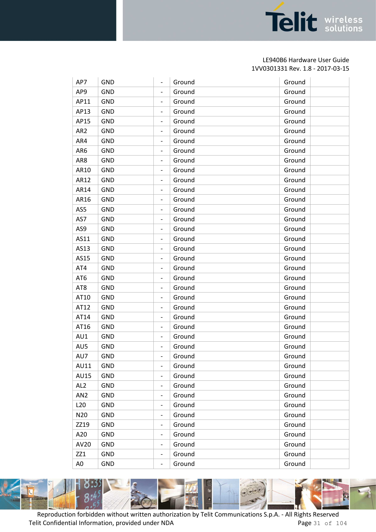

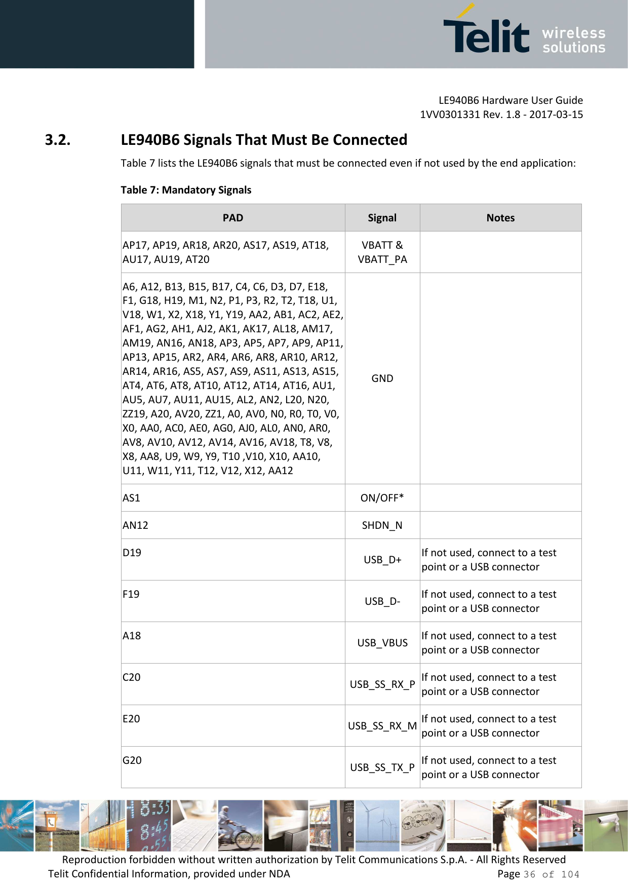
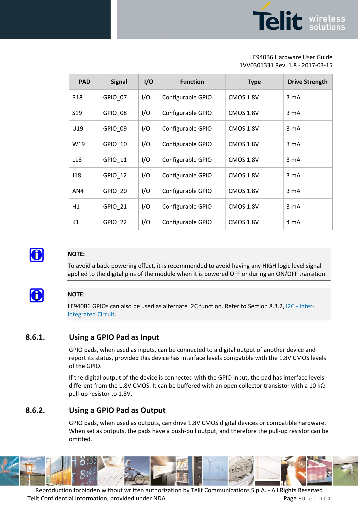
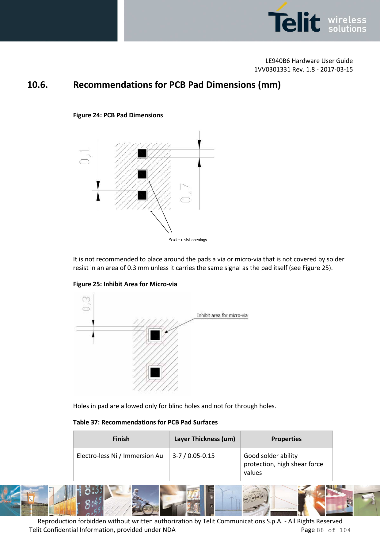
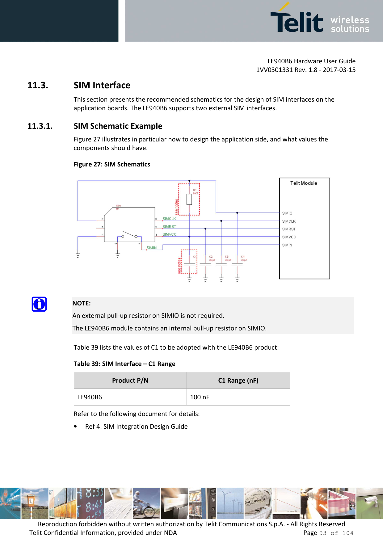
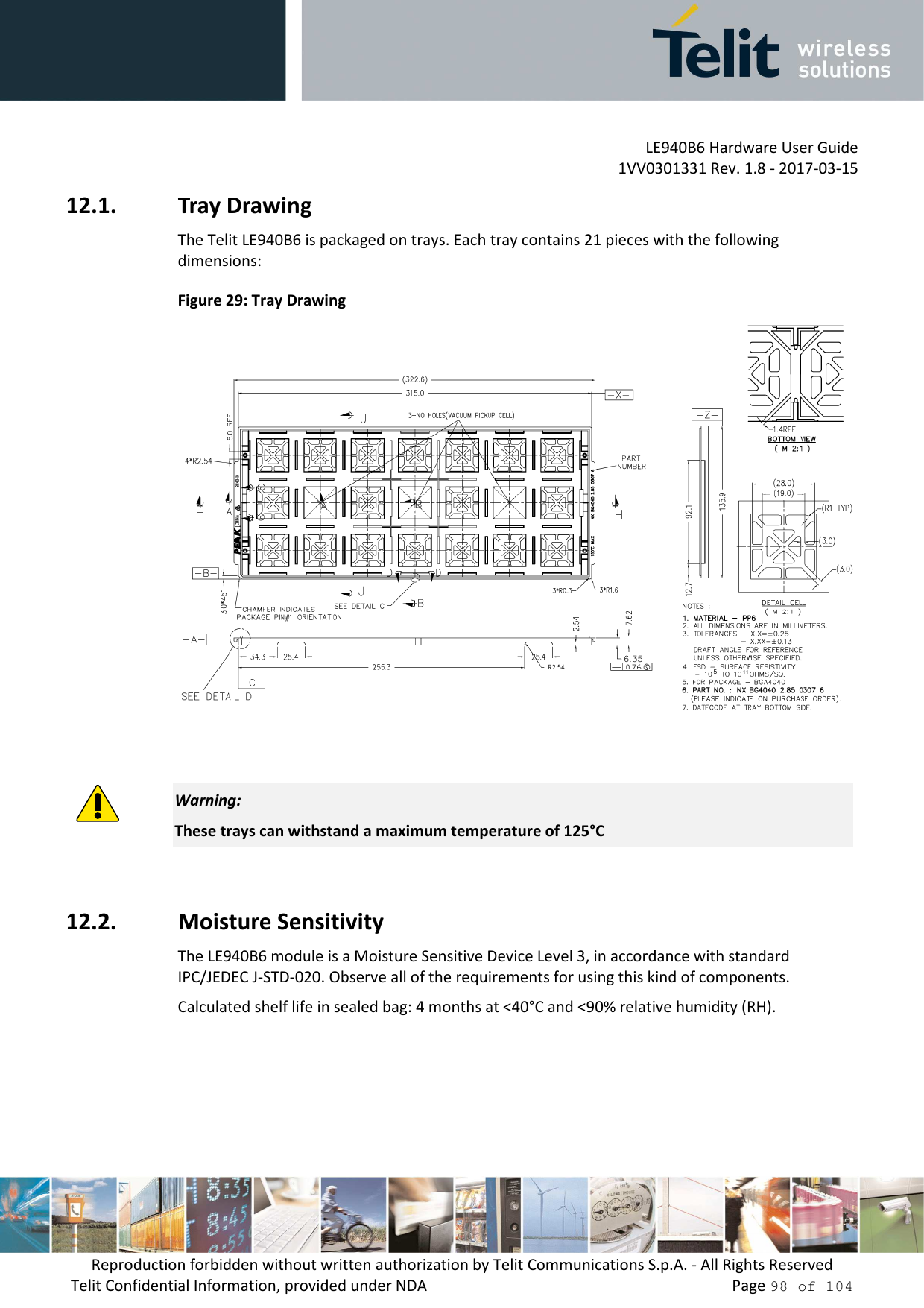
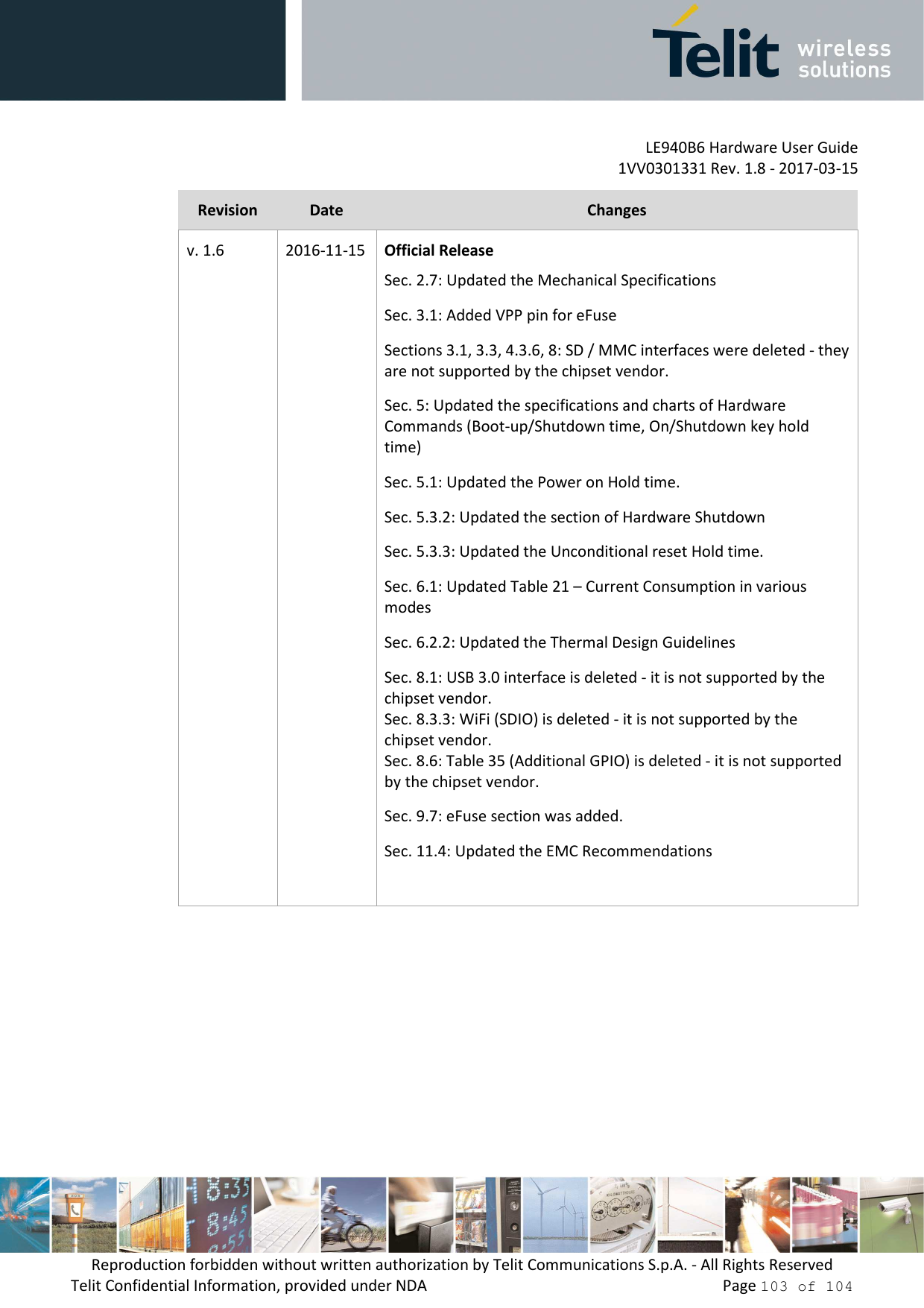
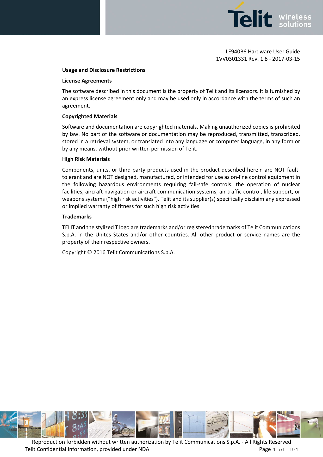
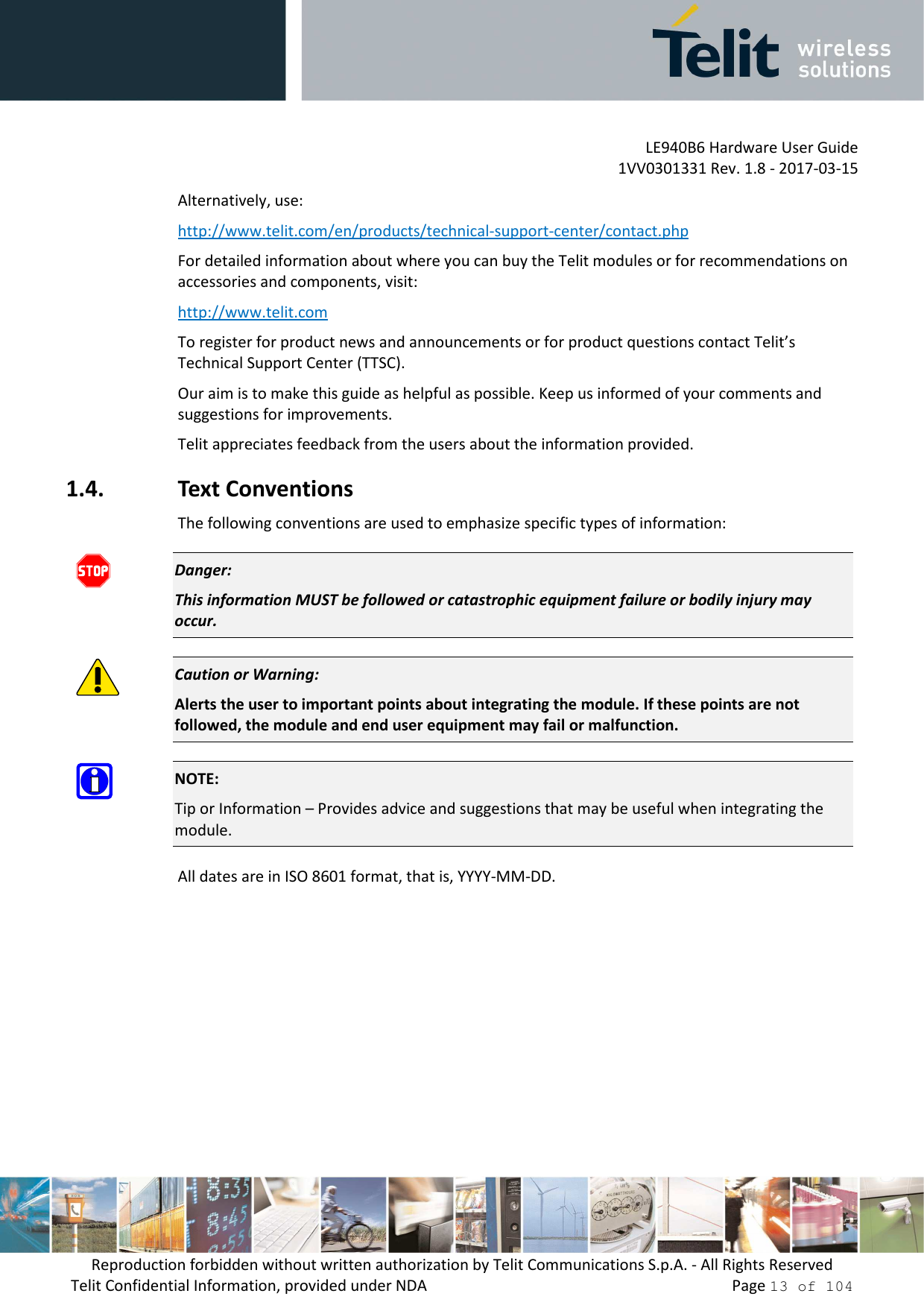
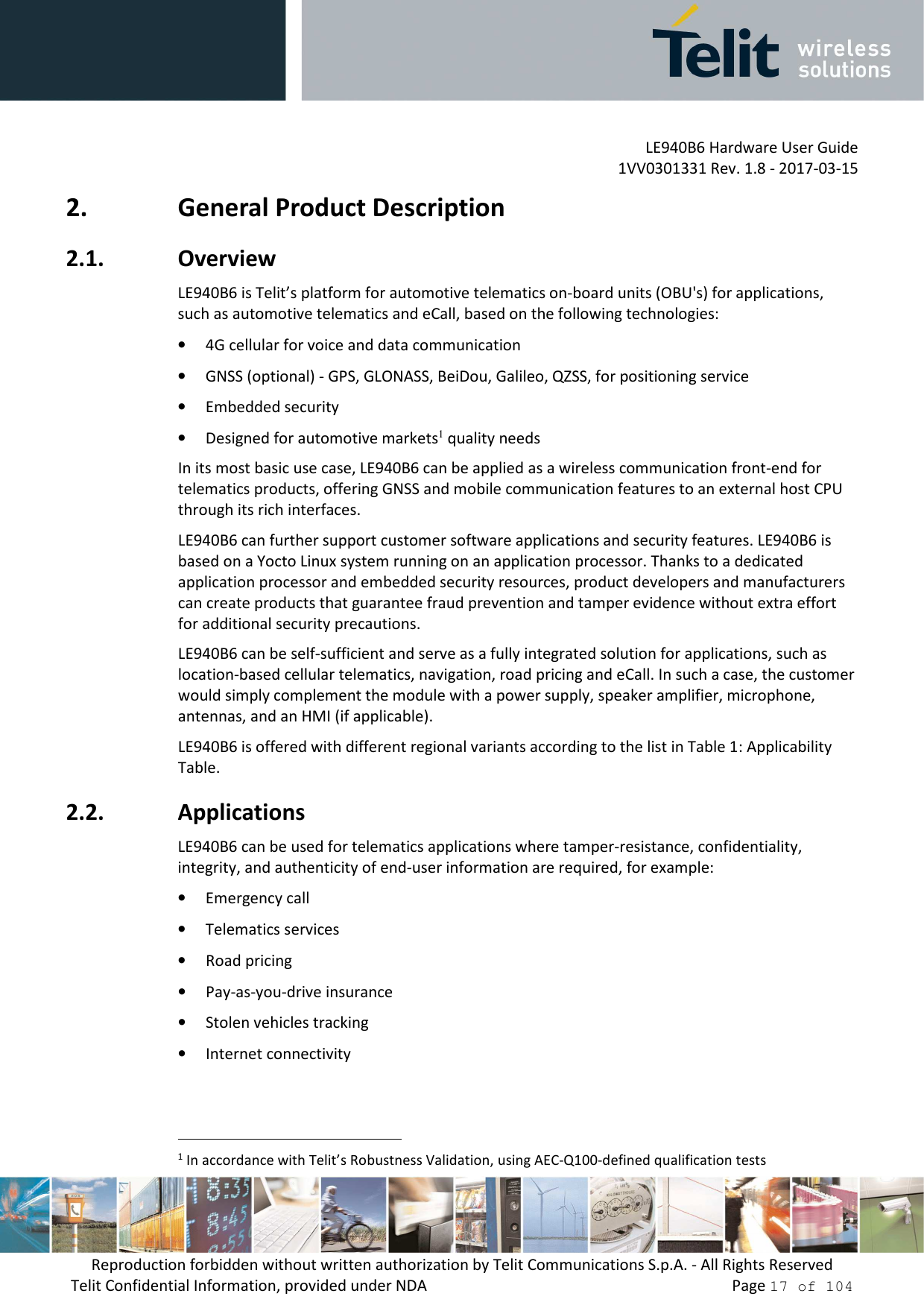
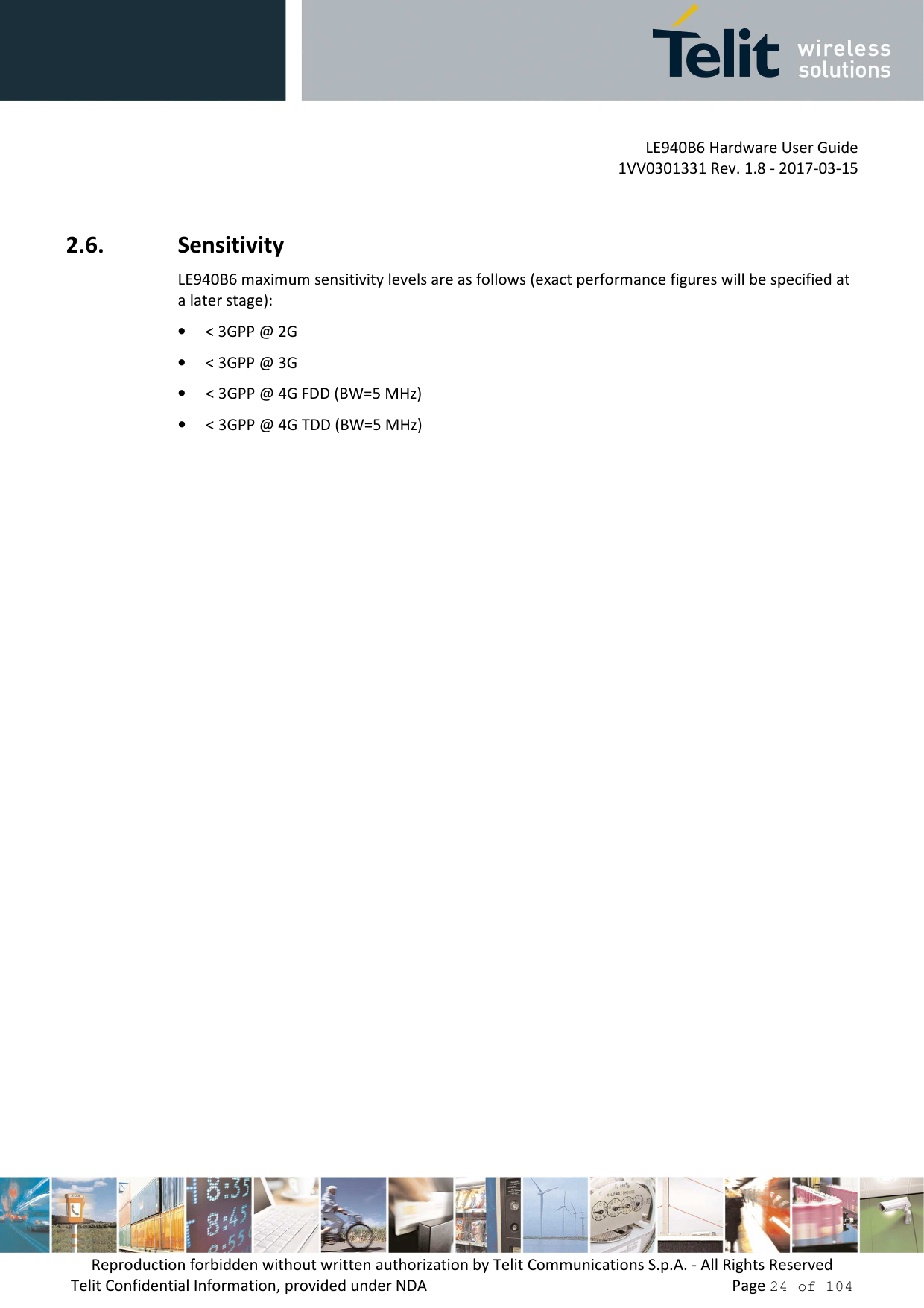
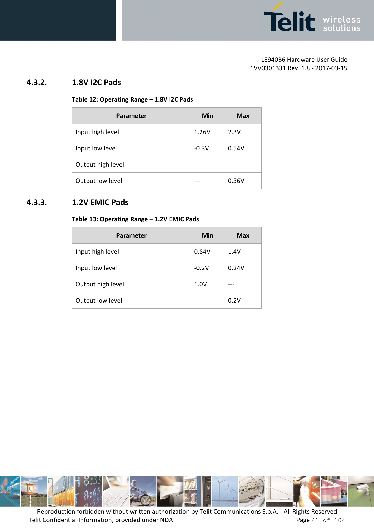
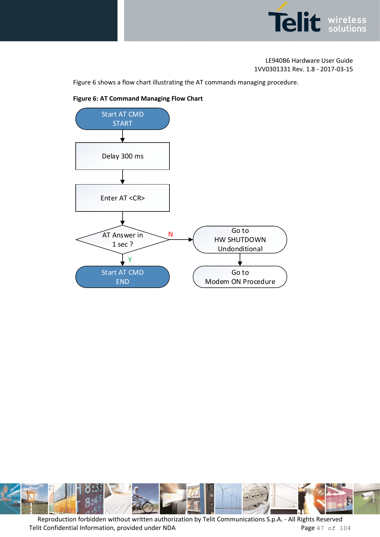
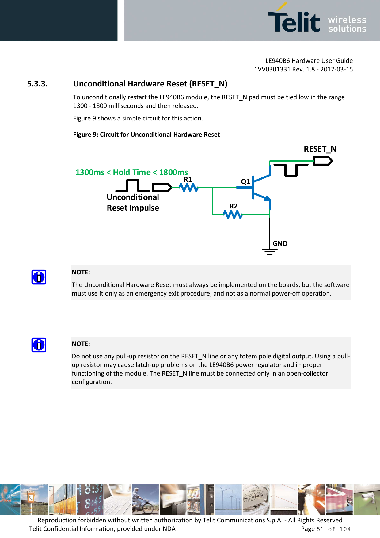
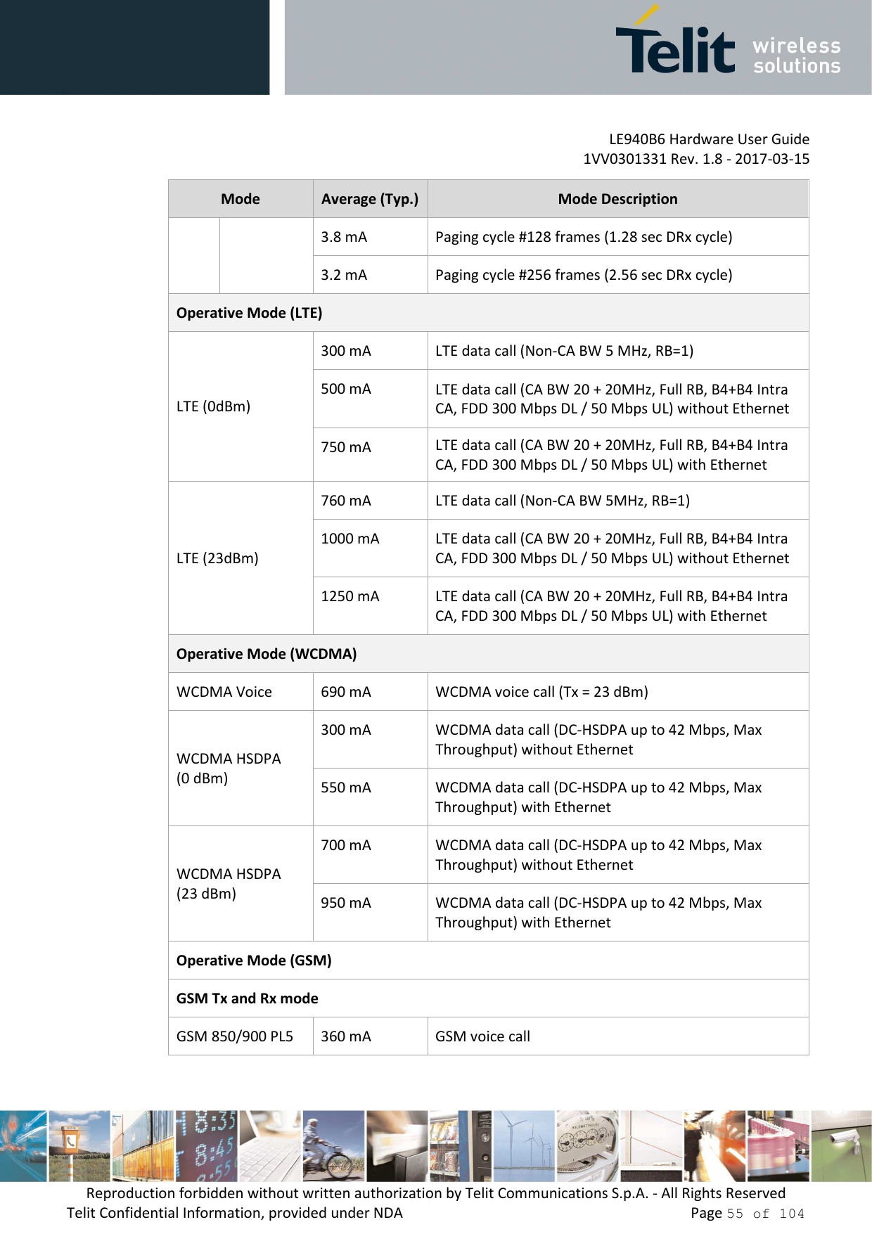
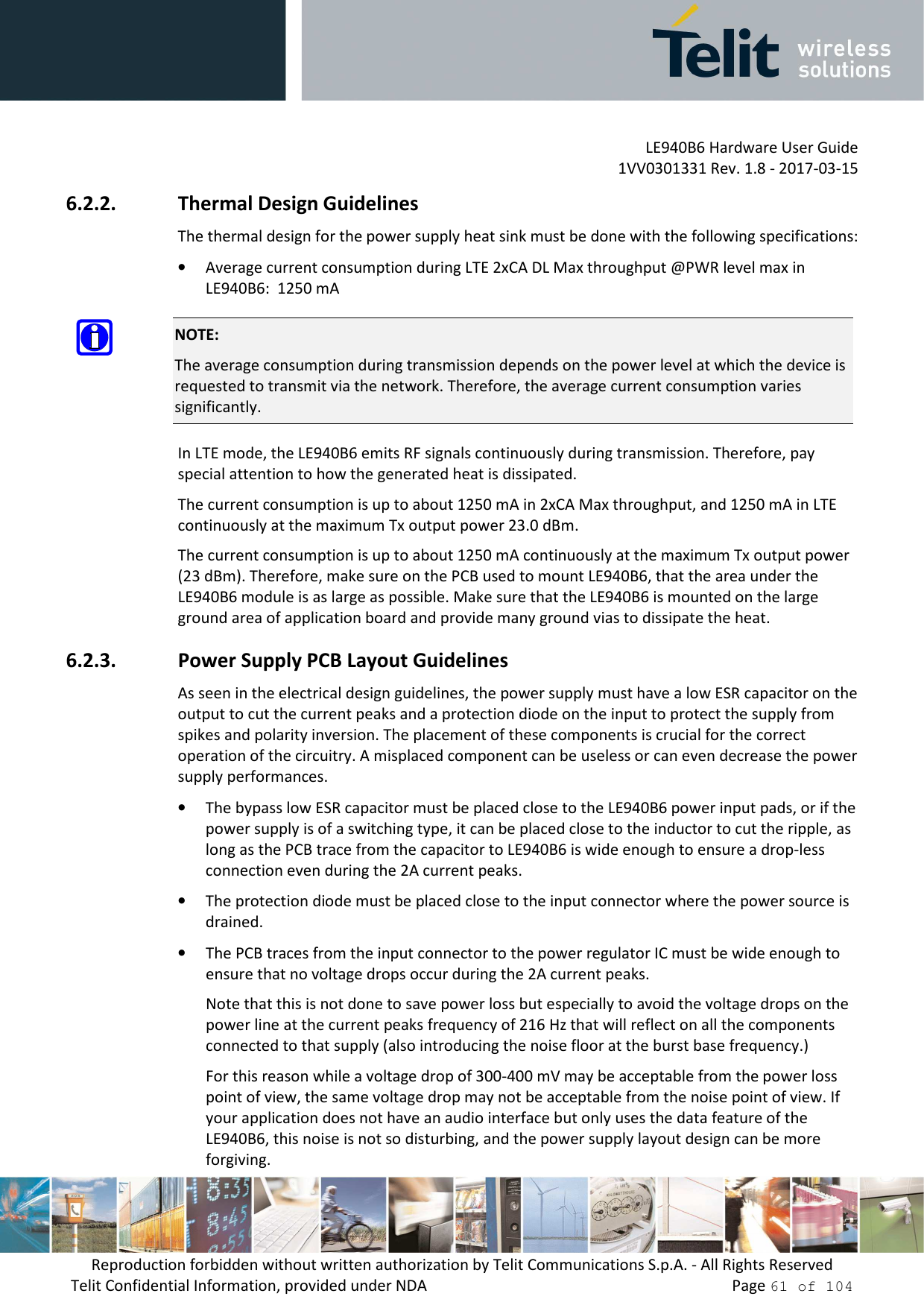
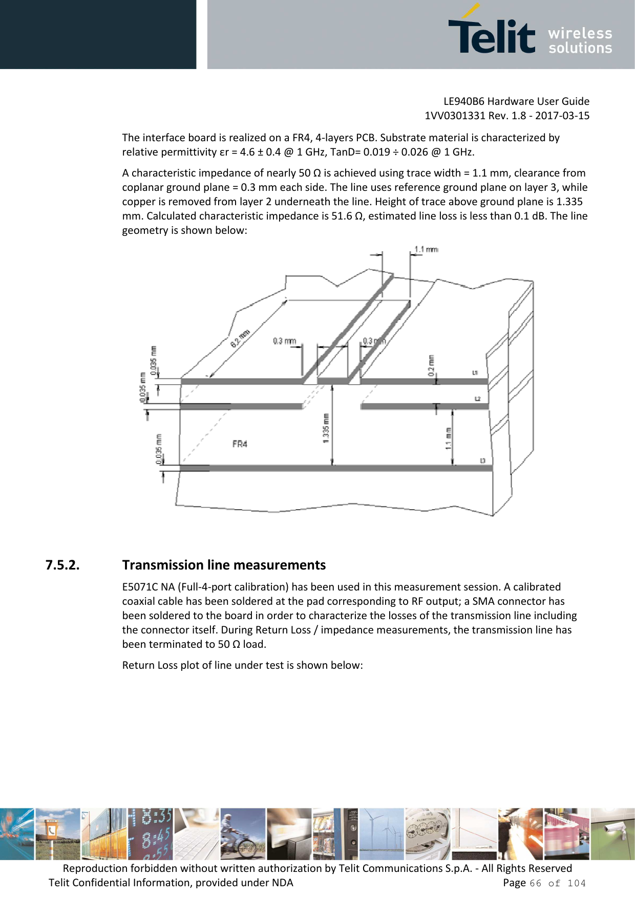
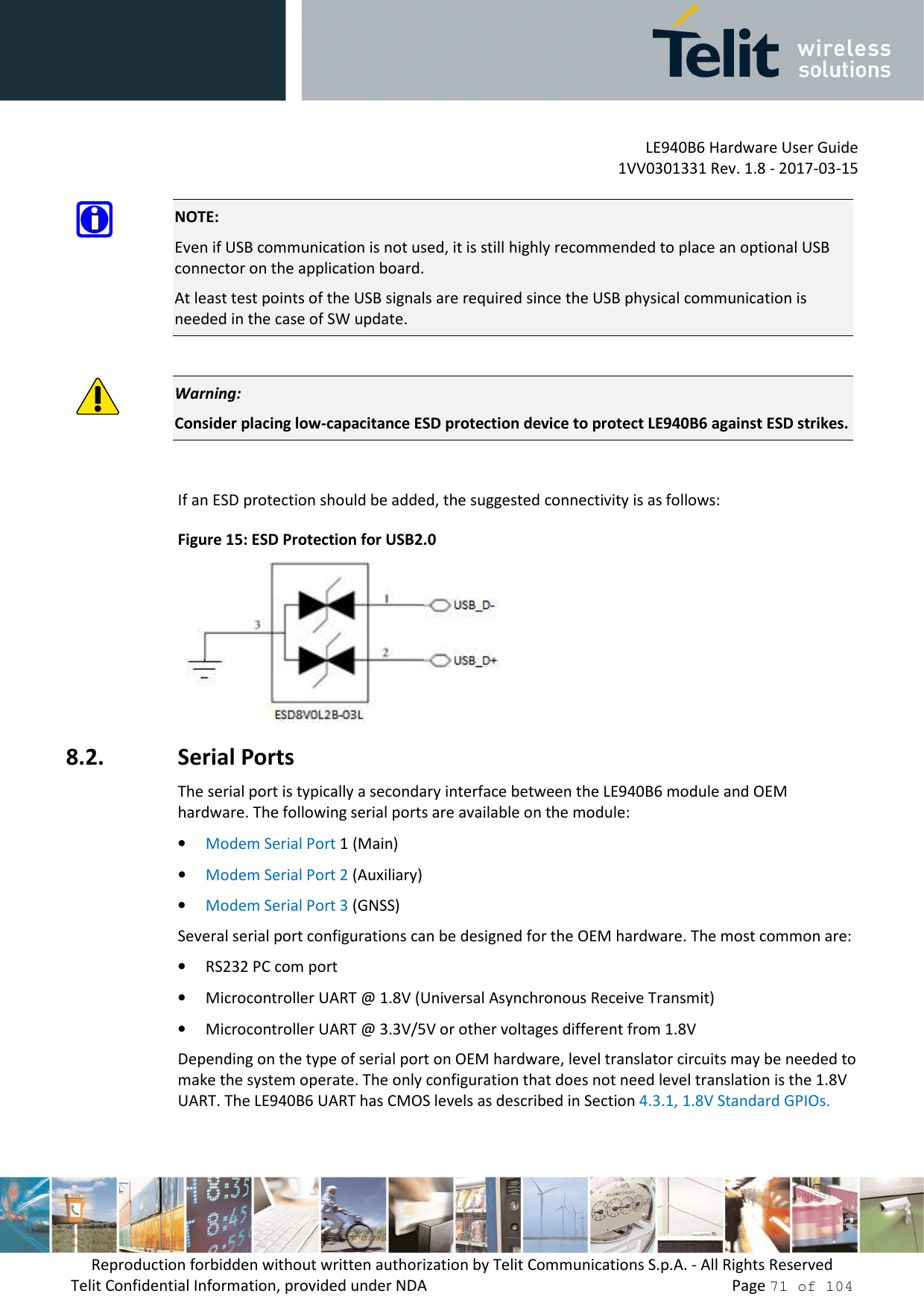
![LE940B6 Hardware User Guide 1VV0301331 Rev. 1.8 - 2017-03-15 Reproduction forbidden without written authorization by Telit Communications S.p.A. - All Rights Reserved Telit Confidential Information, provided under NDA Page 38 of 104 3.3. LGA Pads Layout Figure 2: LGA Pads Layout LE940B6 334 Pads Top View (*) MMC is not supported, and the pins assigned for it became Reserved NOTE: The pin defined as RFU must be considered RESERVED and not connected to any pin in the application. The related area on the application must be kept empty. ZZ A B C D E F G H J K L M N P R S T U V W X Y AA AB AC AD AE AF AG AH AJ AK AL AM AN AP AR AS AT AU AV101GND GND GN D GND GND GND GND GND GN D1010GND RFU RFU RFU RFU RFU GND GND GND GND GND GND GND GND GND GND GND GND GND RFU GND01GND RFU RFU GND GPIO_21GPIO_22GND GND ANT_GPSGND GND GND GND ANT_1 GND GND GND RFU RFU ON_OFF_N GND12MIC1_MT- RFU RFU JTAG_RTCKJTAG_TRST_NJTAG_TMS GND GND GND RFU GND GND GND GND GND GND GND GND GND RFU RFU23RFU MIC1_MT+ GNDJTAG_RESOUT_NJTAG_TCKJTAG_TDOJTAG_TRIGIN GND RFU RFU RFU RFU RFU RFU RFU RFU RFU RFU GND RFU ST AT_LED34EAR1_MT- GND JTAG_TDI RFU RFU JTAG_PTI_CLKJTAG_PTI_DATA0JTAG_PTI_DATA1JTAG_PTI_DATA2JTAG_PTI_DATA3RFU RFU RFU RFU RFU RFU RFU GPIO_20GND GND RFU45RFU EAR1_MT+ADC_IN1JTAG_TRIGOUT RFU GND GND GND56GND GND ADC_IN2MIC_BIASRFU GND GND RFU67RFU SIMIN1 GND ADC_IN3RFU GND GND GND78SIMVCC1DVI_RX RFU ETH_RST_N GND GND GND GND RESET_NGND GND GND89RFU SIMIO1 DVI_TX GPIO_01GND GND GND UART3_TXD GND GND ANT_DIV_1910SIMCLK1DVI_CLKGPIO_02ETH_INT_N GND GND GND GND SW_RDY GND GND GND1011RFU SIMRST1DVI_WA0GPIO_03GND GND GND UART3_RXD GND GND GND1112GND RFU GPIO_04MAC_MDIO GND GND GND GND SHDN_N GND GND GND1213RFU GND I2C_SDA GPIO_05UART3_RTS GND GND RFU1314RFU I2C_SCL GPIO_06MAC_MDCRFU GND GND GND1415RFU GND SIMVCC2RFU UART3_CTS GND GND GND1516RFU SIMCLK2SIMIO2 MAC_TXEN_ER RFU MAC_GTX_CLKMAC_TXD[3]MAC_TXD[2]MAC_TXD[1]MAC_TXD[0]MAC_RXDV_ER RFU MAC_RX_CLKMAC_RXD[3]MAC_RXD[2]MAC_RXD[1]MAC_RXD[0] GND GND GND GND1617RFU GND SIMRST2VRTC VPP VIO _1.8VRFU VAUX/PWRMON RFU RFU RFU RFU RFU RFU RFU RFU GND GND VBATT VBATT_PAVBATT_PA1718USB_VBUS SIMIN2 GND GND GPIO_12GPIO_11SPI_CS GP IO_07GND GND GND C105/RTSC108/DTRC109/DCDC107/DSRC125/RING GND GND VBATT VBATT_PA GND1819GND RFU USB_D+ USB_D- GND SPI _MOSISPI_ MISOSPI_CLKGPIO_08GPIO_09GPIO_10GND TXD_AUXRXD_AUXC104/RXDC103/TXDC106/CTSGND VBATT VBATT_PAVBATT_PA1920GND RFU RFU RFU RFU GND GND RFU RFU RFU RFU RFU RFU RFU RFU RFU RFU RFU VBATT VBATT_PA GND20102GND GND GN D GND GND GND GND GND GN D102ZZ A B C D E F G H J K L M N P R S T U V W X Y AA AB AC AD AE AF AG AH AJ AK AL AM AN AP AR AS AT AU AVLE940B6 (40 mm X 40 mm) Form Factor Pin MAPTOP VIEW](https://usermanual.wiki/Telit-Communications-S-p-A/LE940B6NA/User-Guide-3334482-Page-38.png)
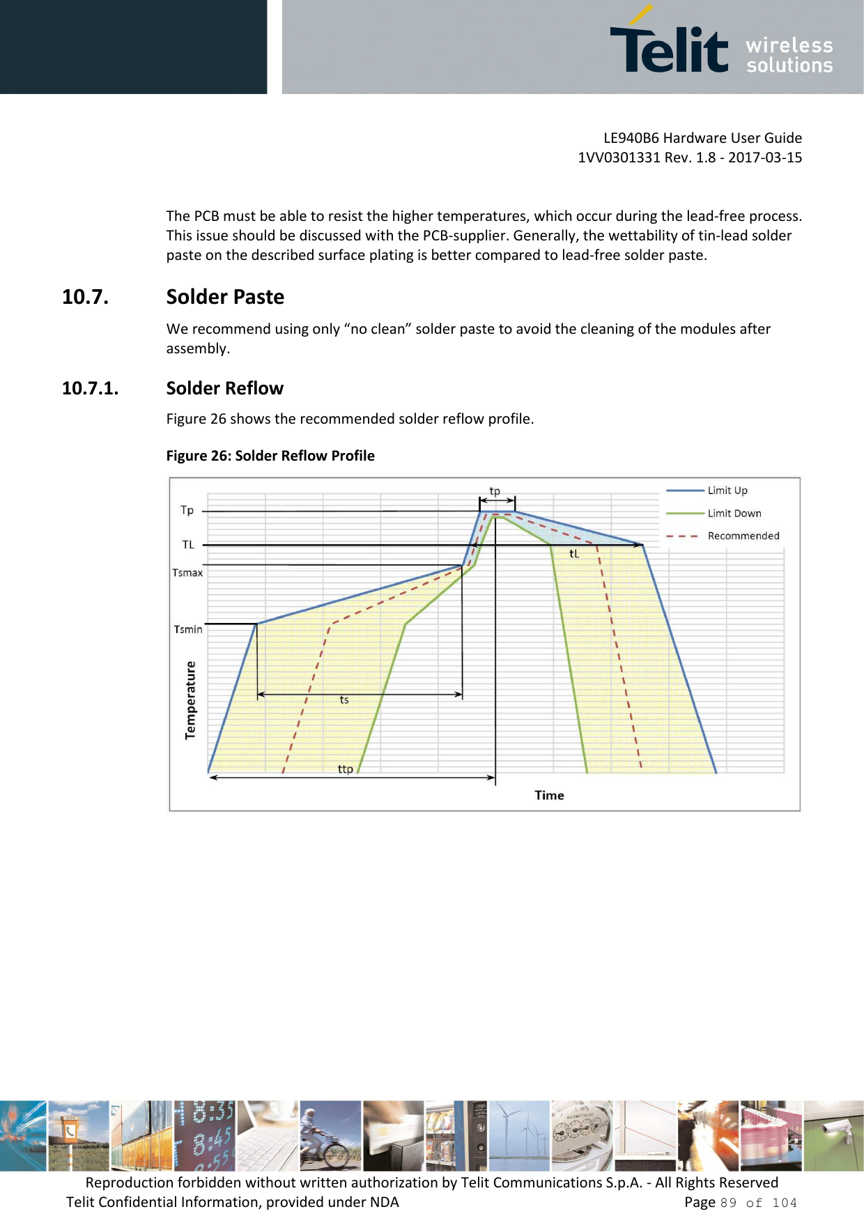
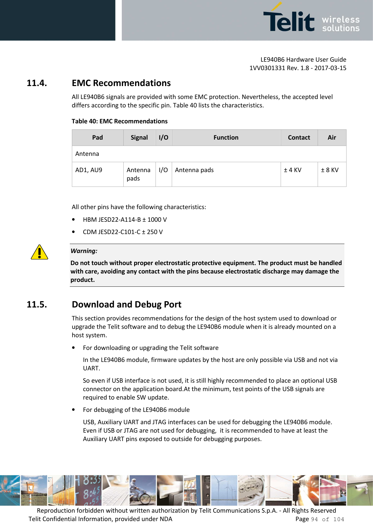
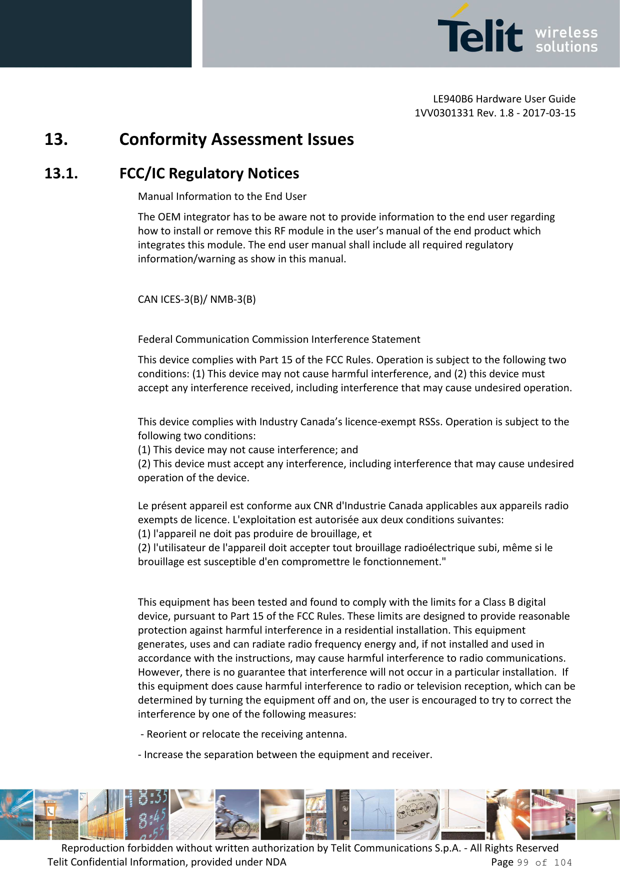
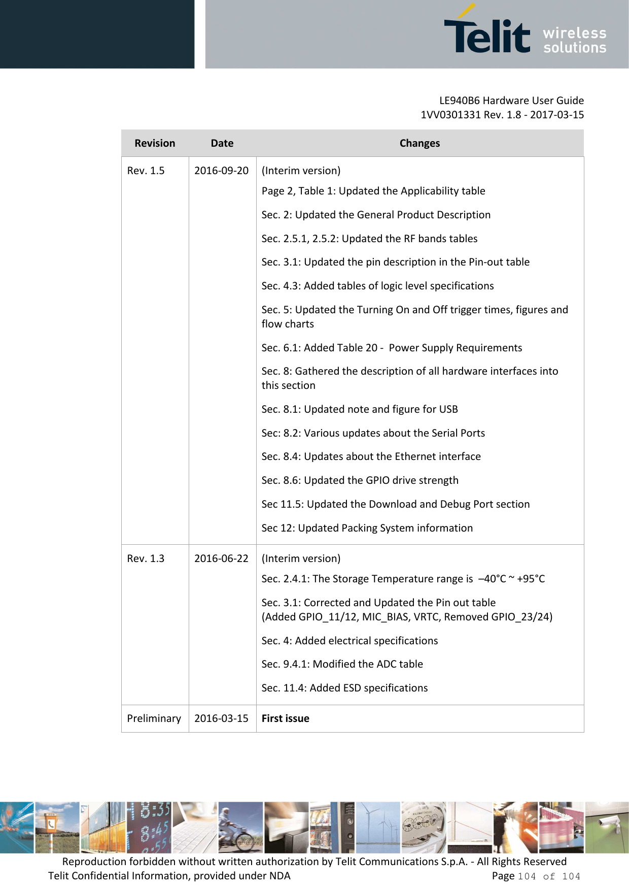
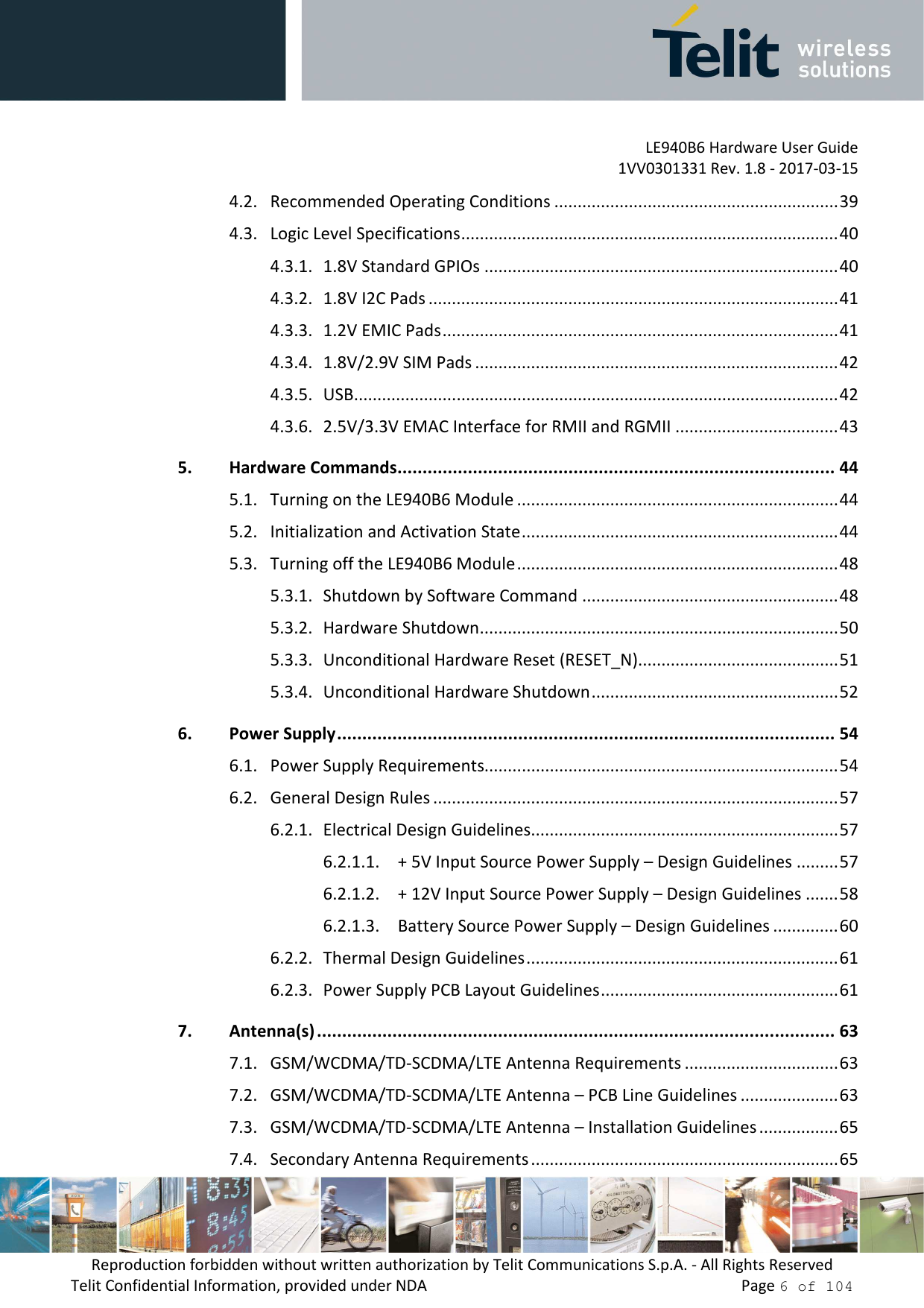
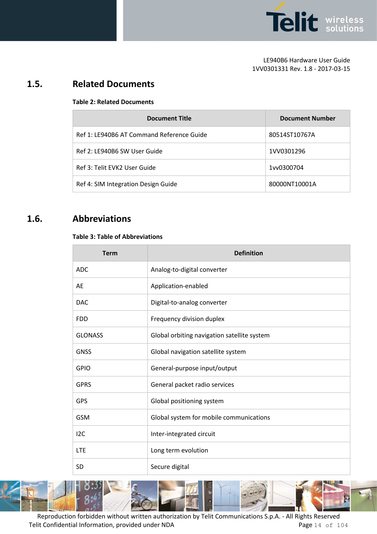
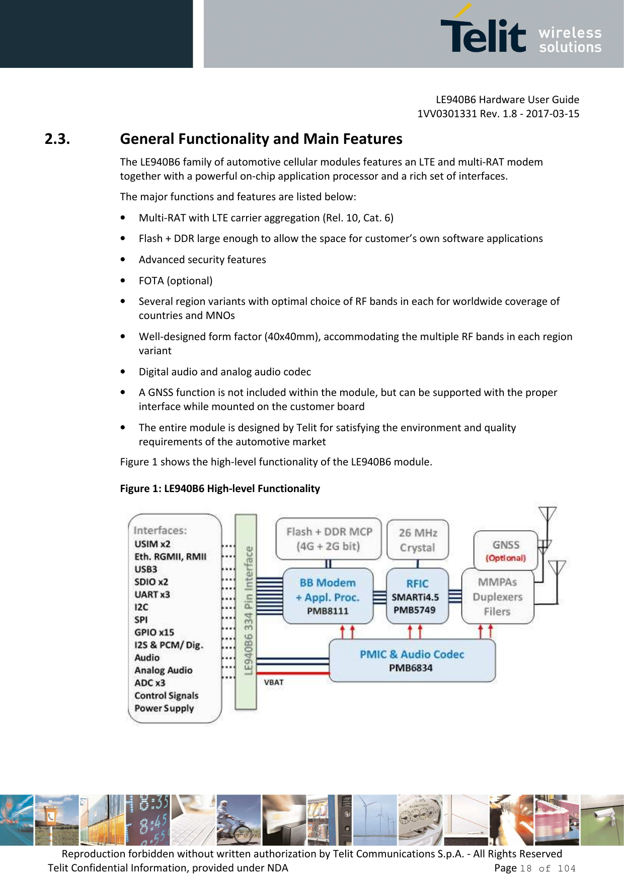
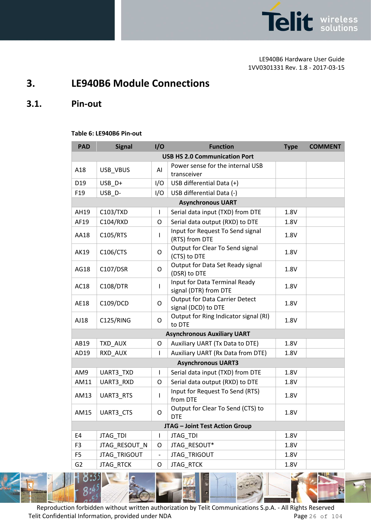
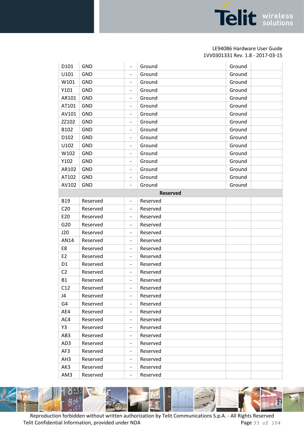
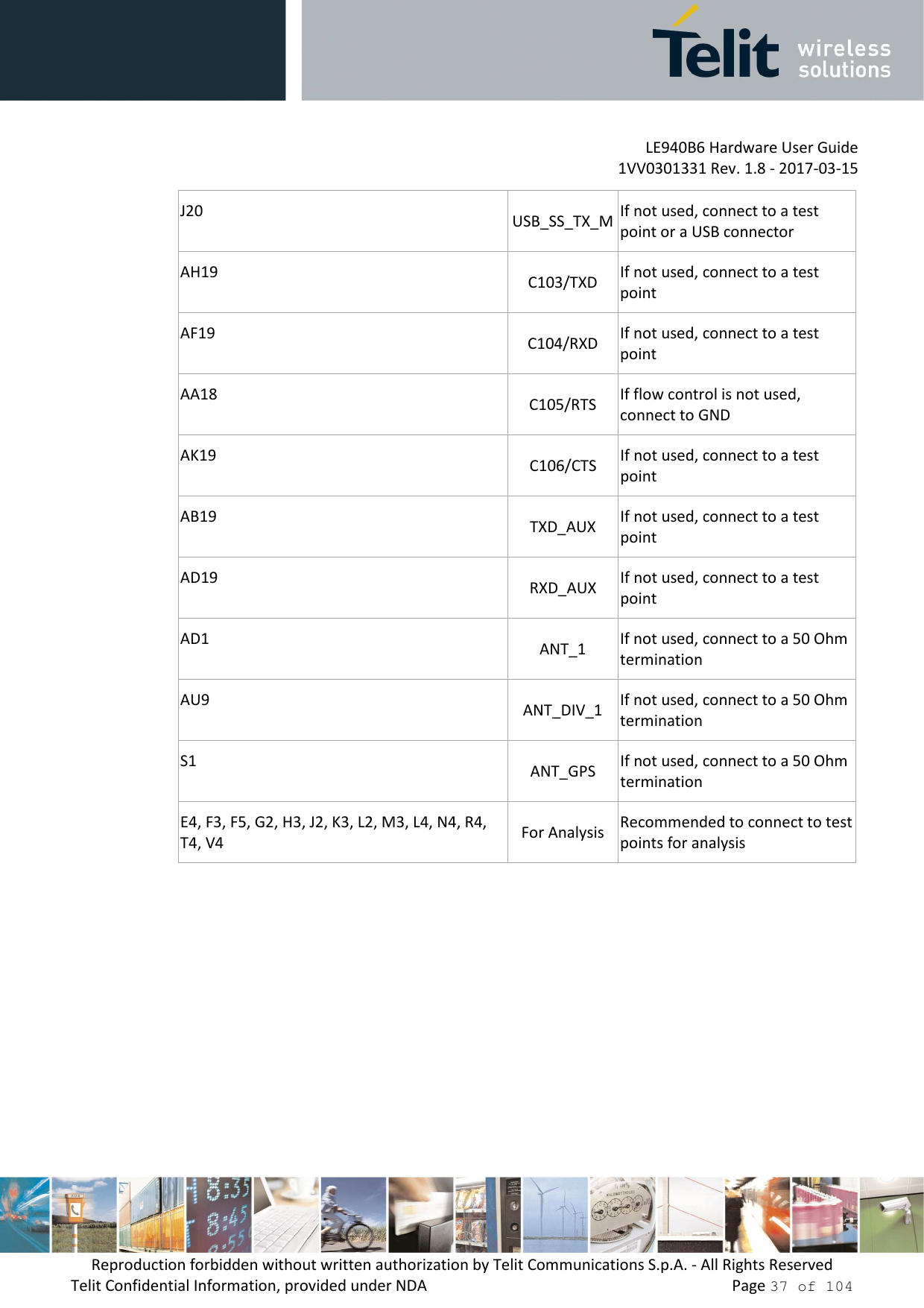
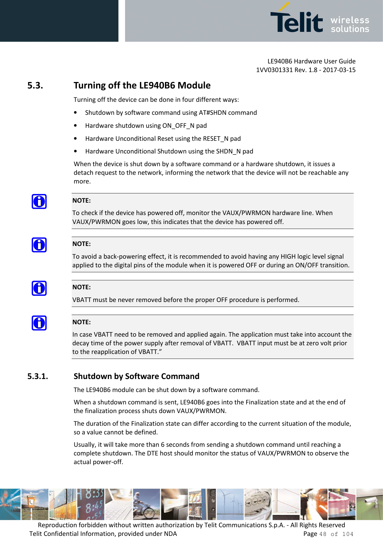
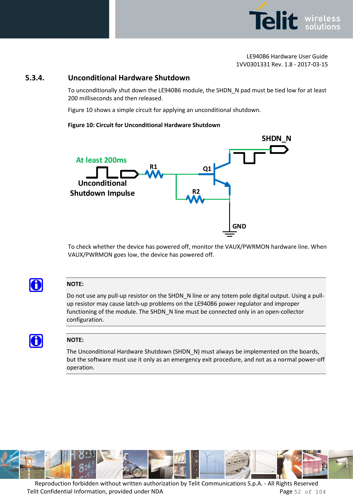
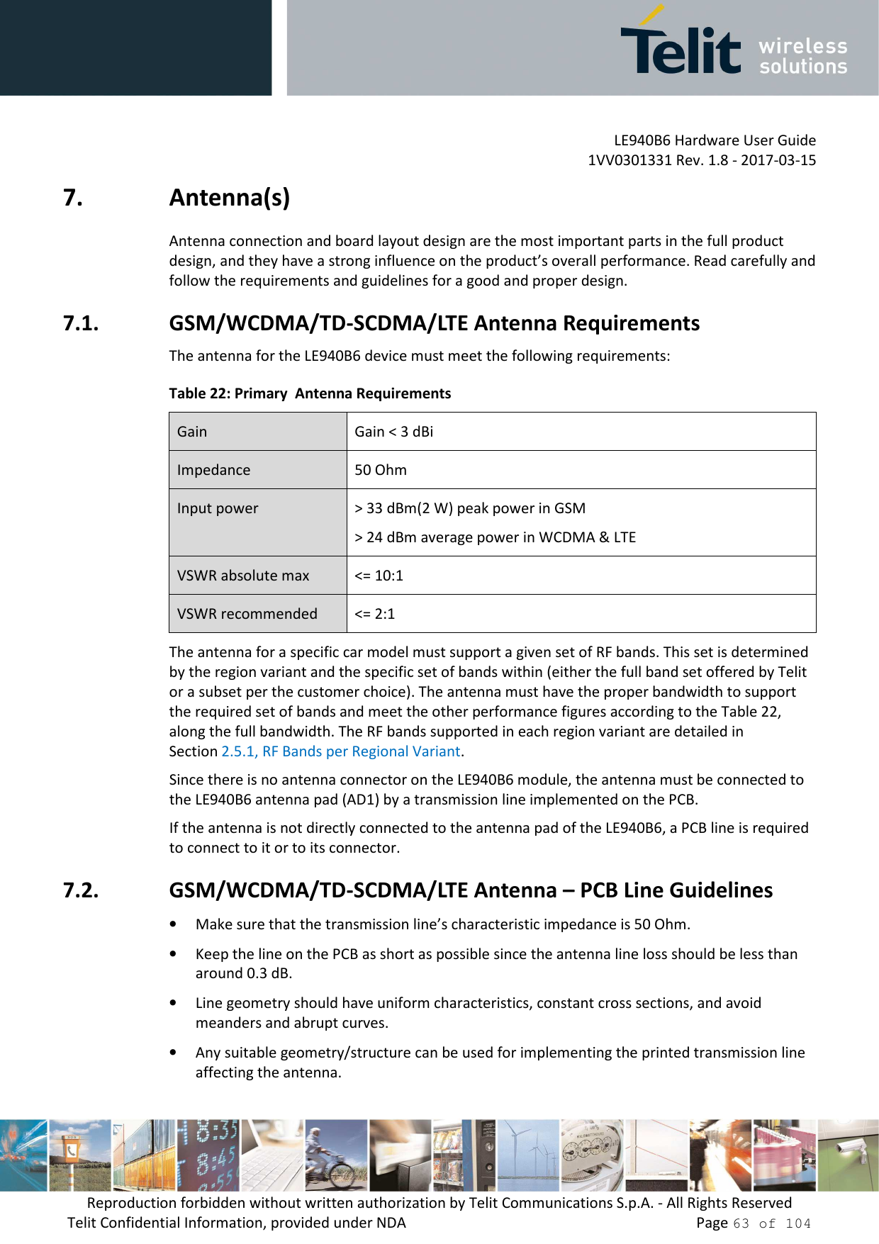
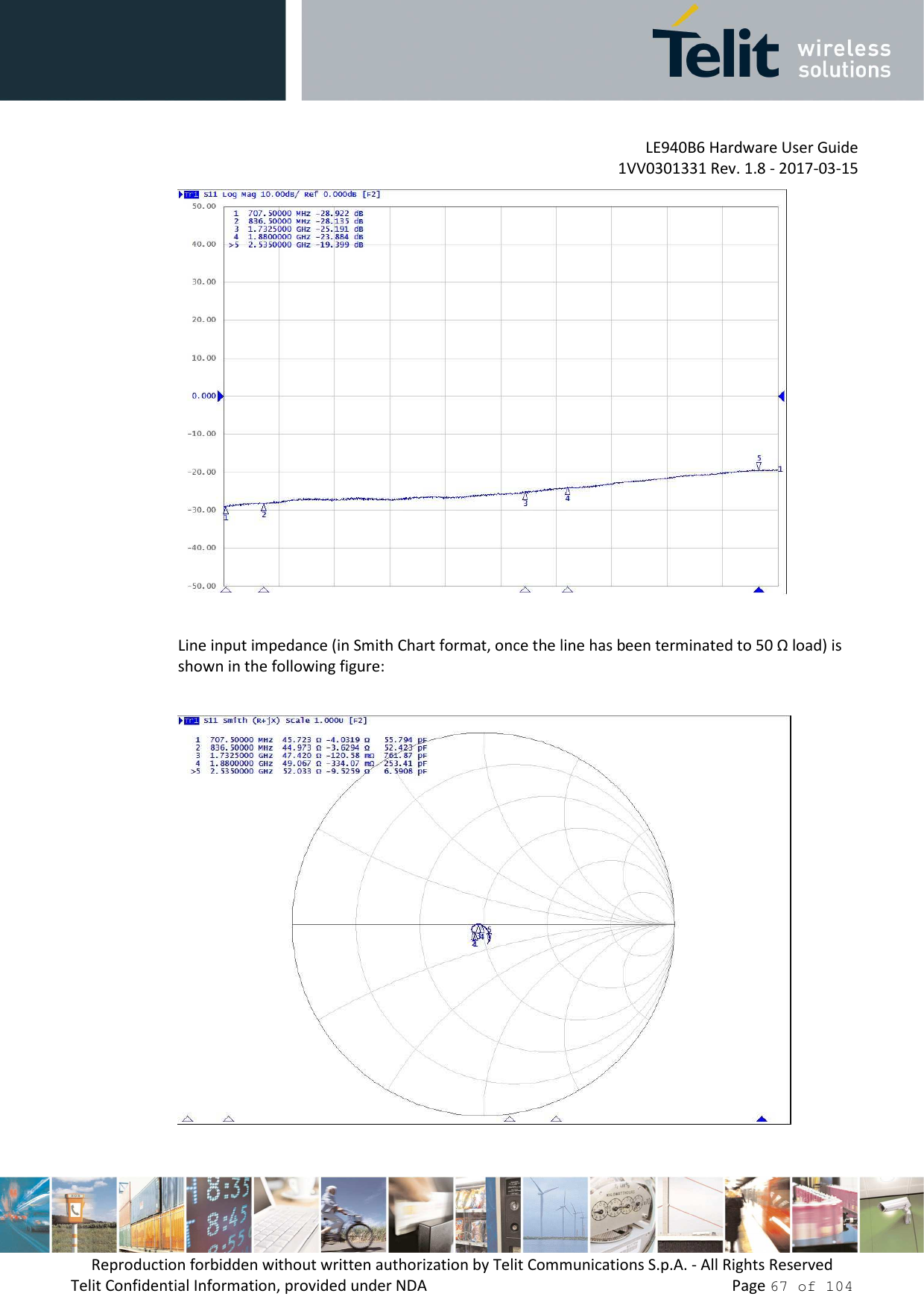
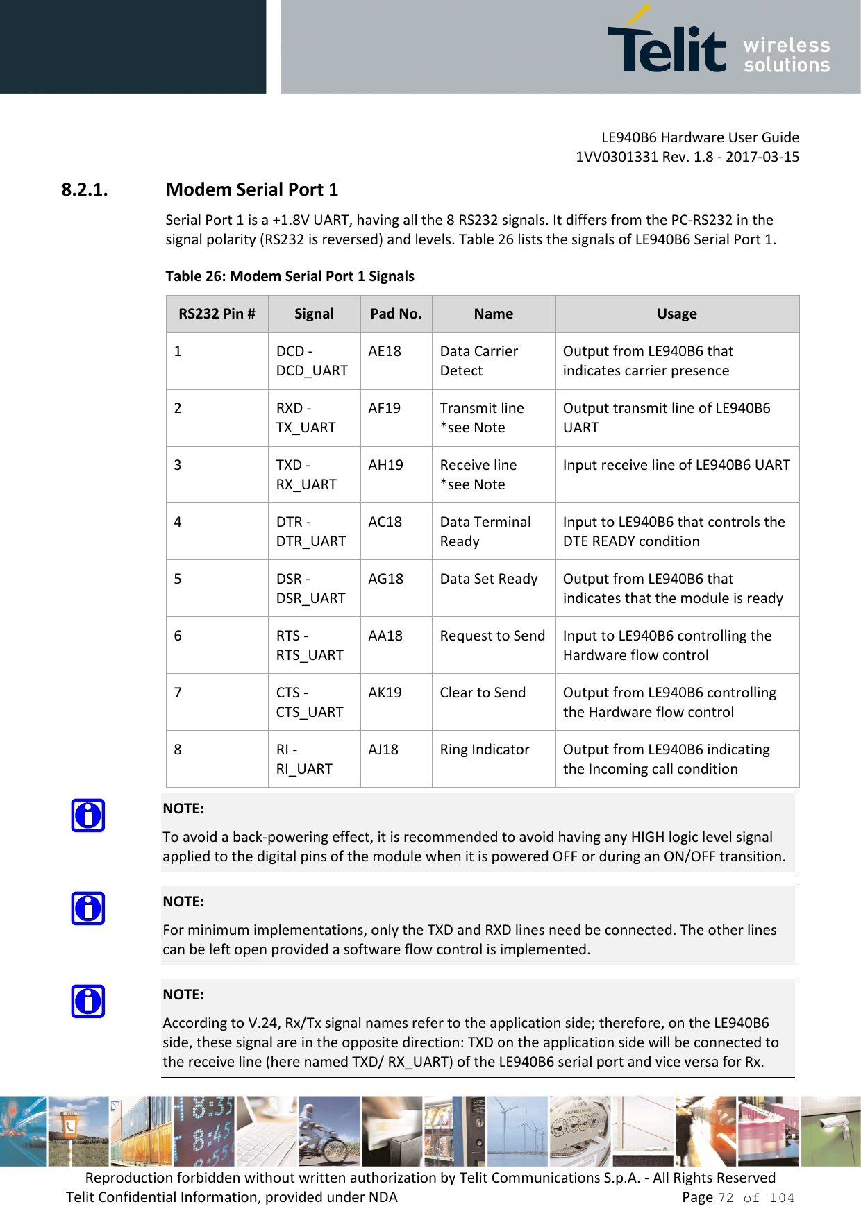
![LE940B6 Hardware User Guide 1VV0301331 Rev. 1.8 - 2017-03-15 Reproduction forbidden without written authorization by Telit Communications S.p.A. - All Rights Reserved Telit Confidential Information, provided under NDA Page 39 of 104 4. Electrical Specifications 4.1. Absolute Maximum Ratings – Not Operational Caution: A deviation from the value ranges listed below may harm the LE940B6 module. Table 8: Absolute Maximum Ratings – Not Operational Symbol Parameter Min Max Unit VBATT Battery supply voltage on pin VBATT -0.3 +6.0 [V] VBATT_PA Battery supply voltage on pin VBATT_PA -0.3 +6.0 [V] 4.2. Recommended Operating Conditions Table 9: Recommended Operating Conditions Symbol Parameter Min Typ Max Unit Tamb Ambient temperature -40 +25 +85 [°C] VBATT Battery supply voltage on pin VBATT 3.4 3.8 4.2 [V] VBATT_PA Battery supply voltage on pin VBATT_PA 3.4 3.8 4.2 [V] IBATT_PA + IBATT Peak current to be used to dimension decoupling capacitors on pin VBATT_PA - 80 2000 [mA]](https://usermanual.wiki/Telit-Communications-S-p-A/LE940B6NA/User-Guide-3334482-Page-39.png)
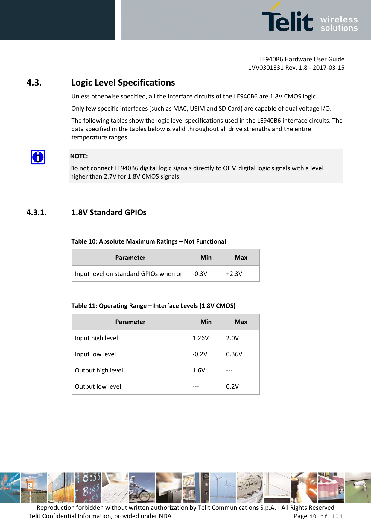

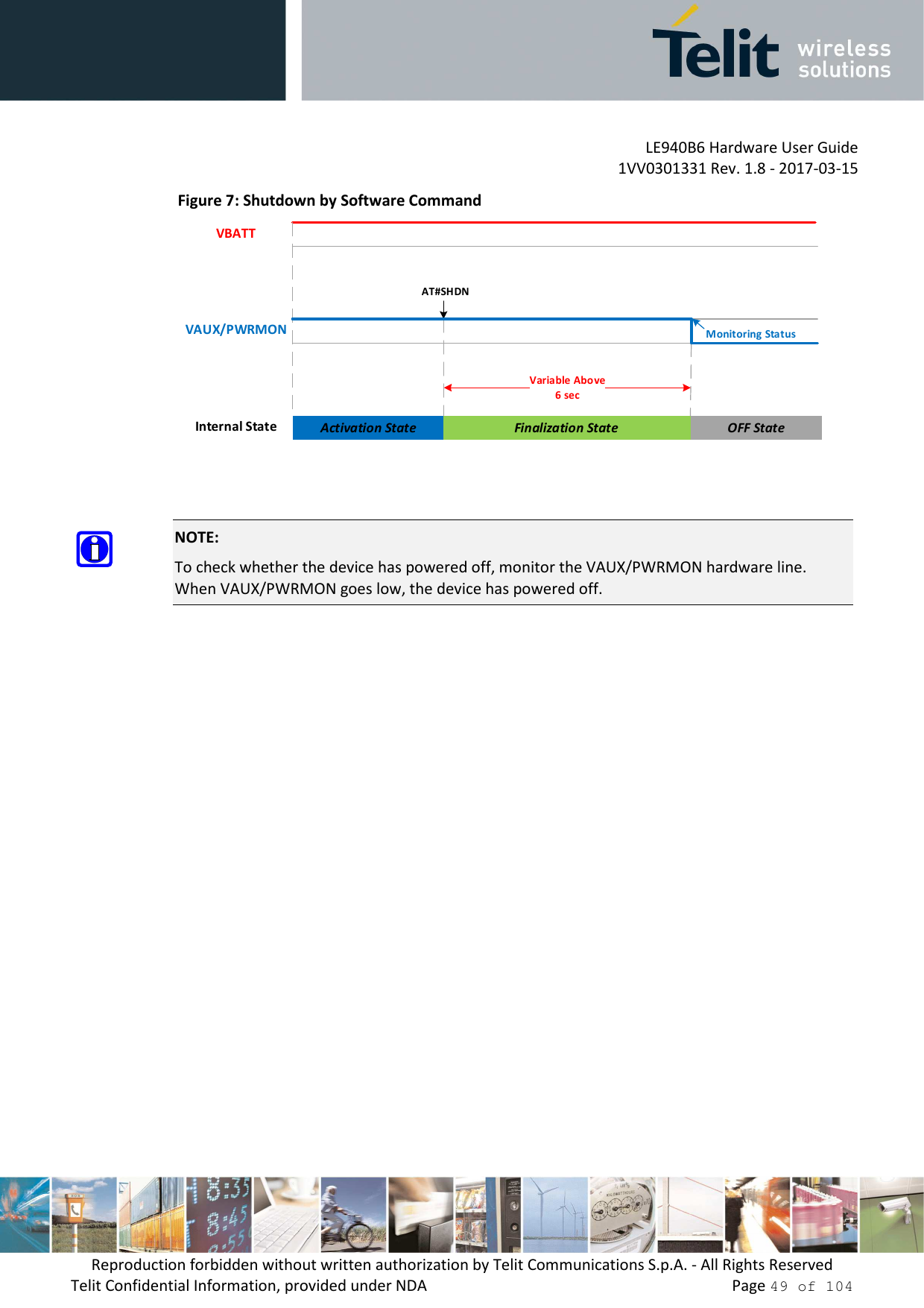
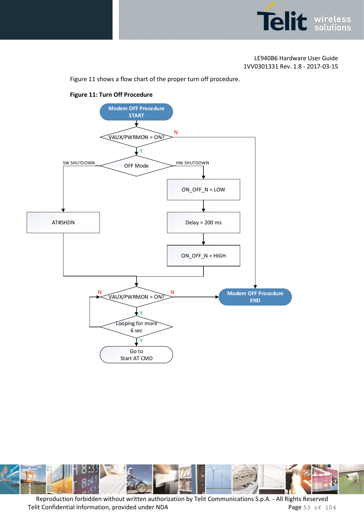


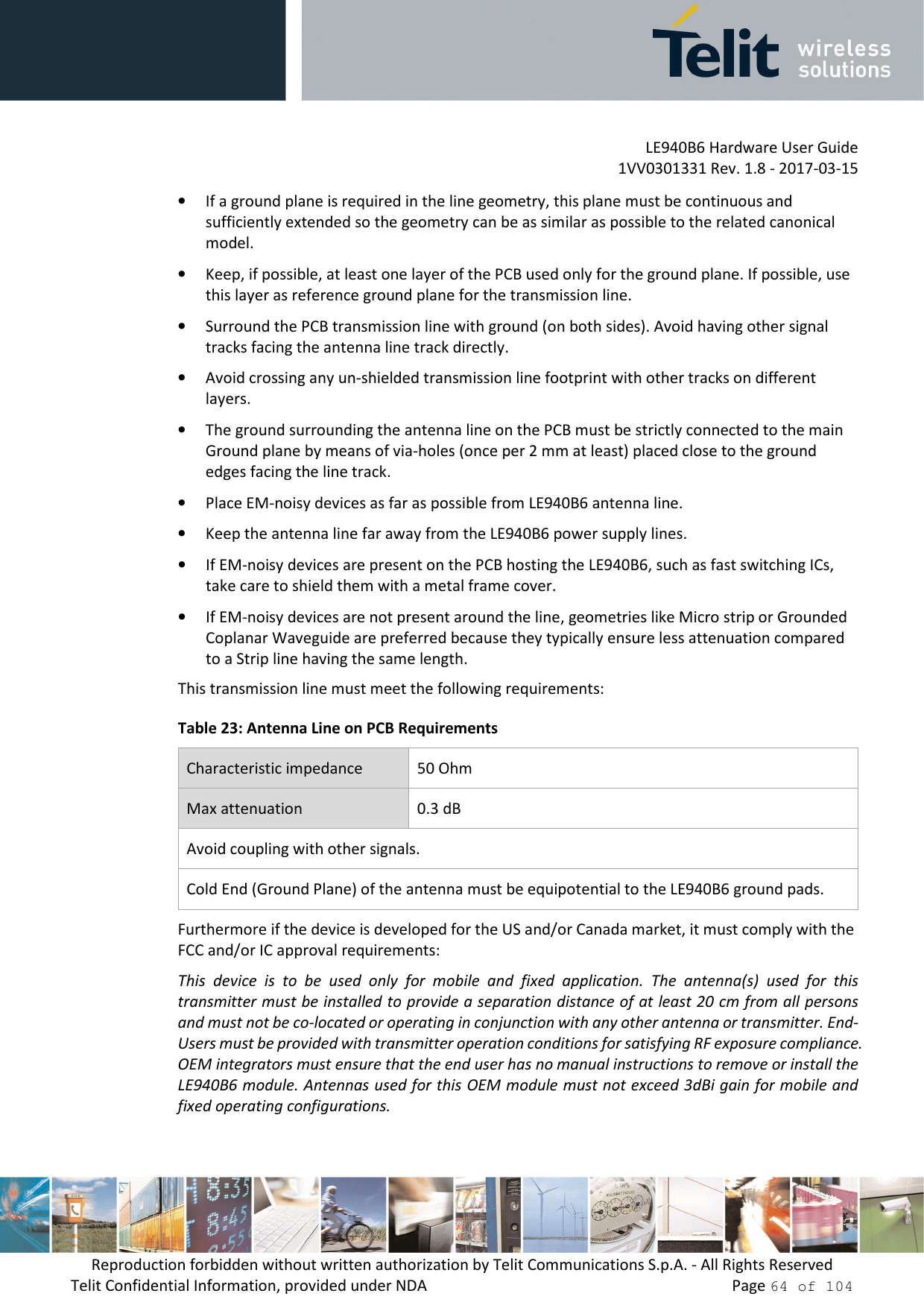

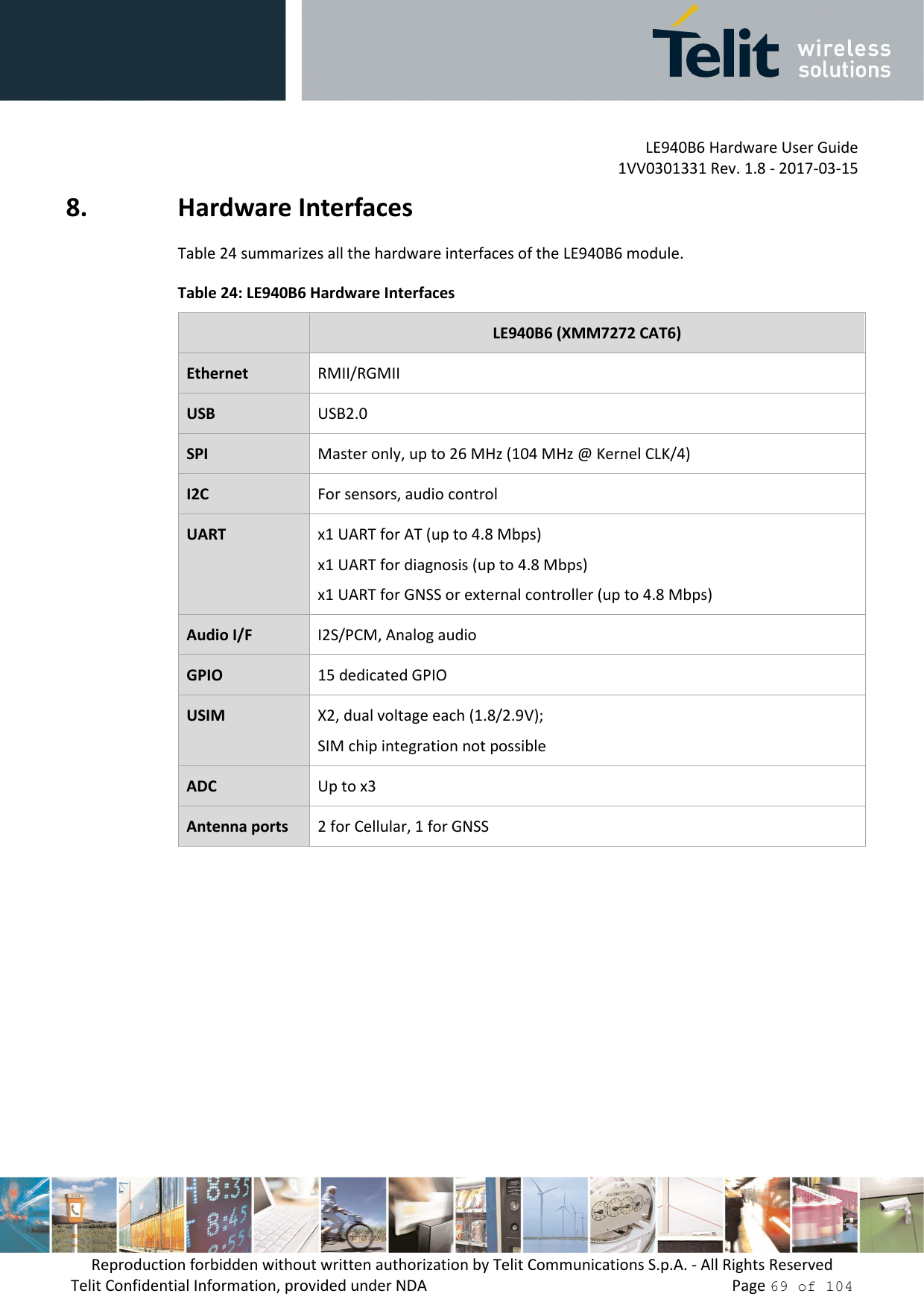
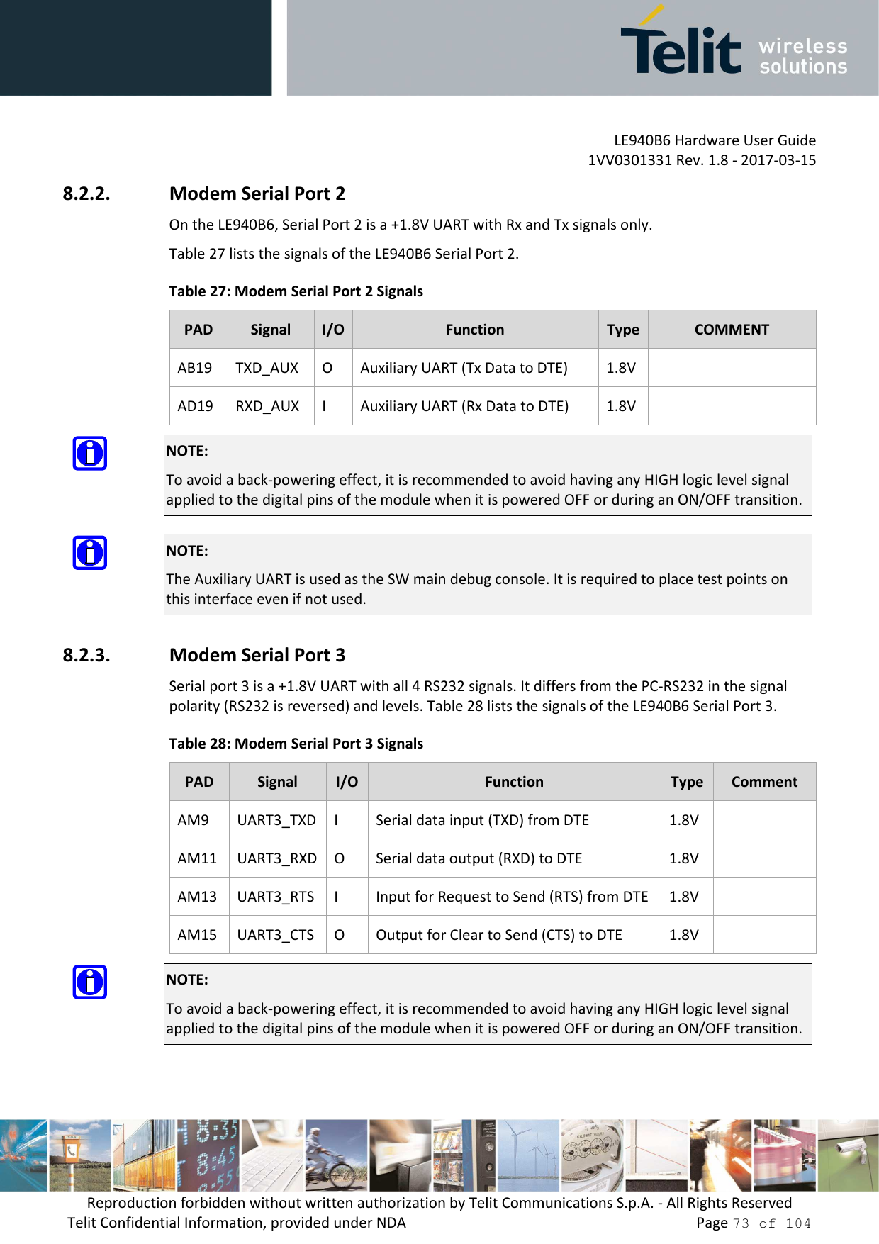
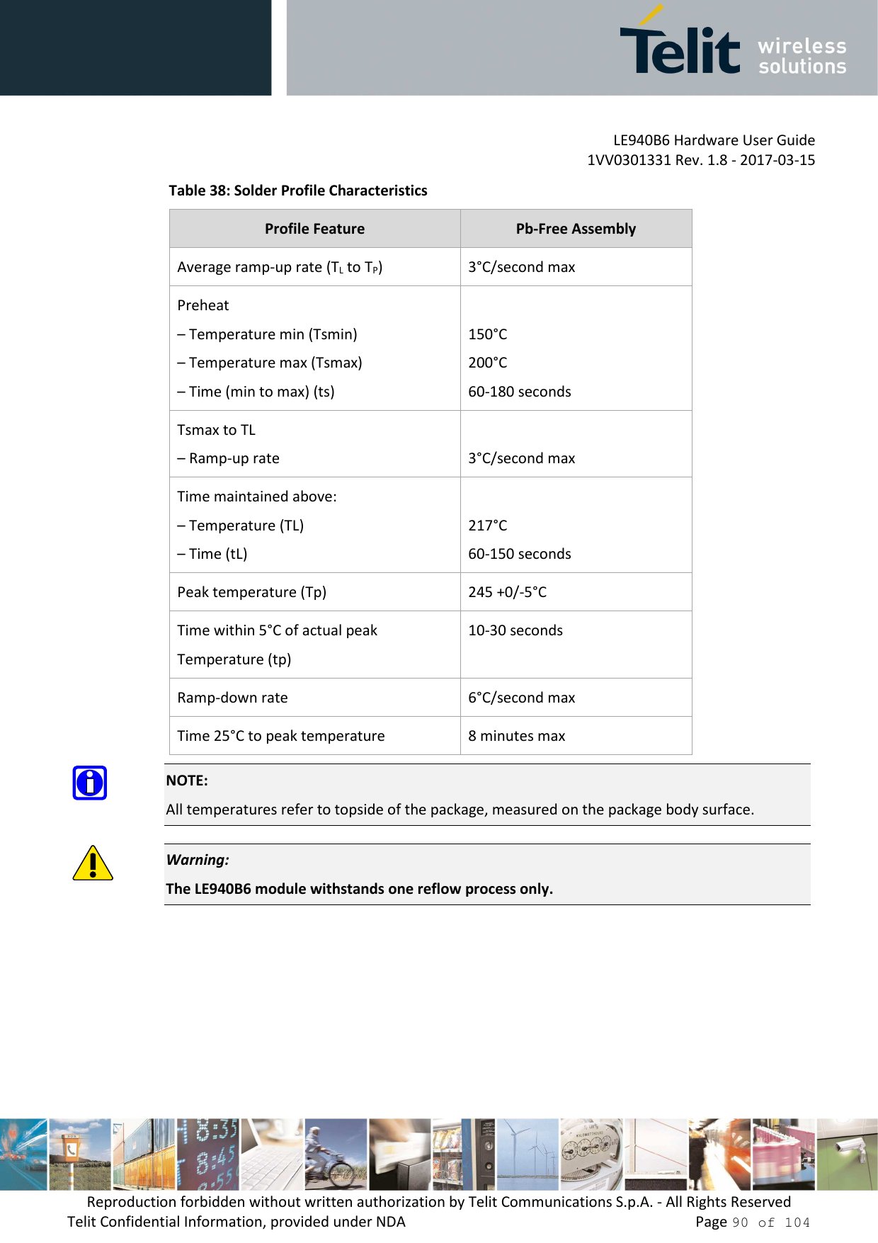
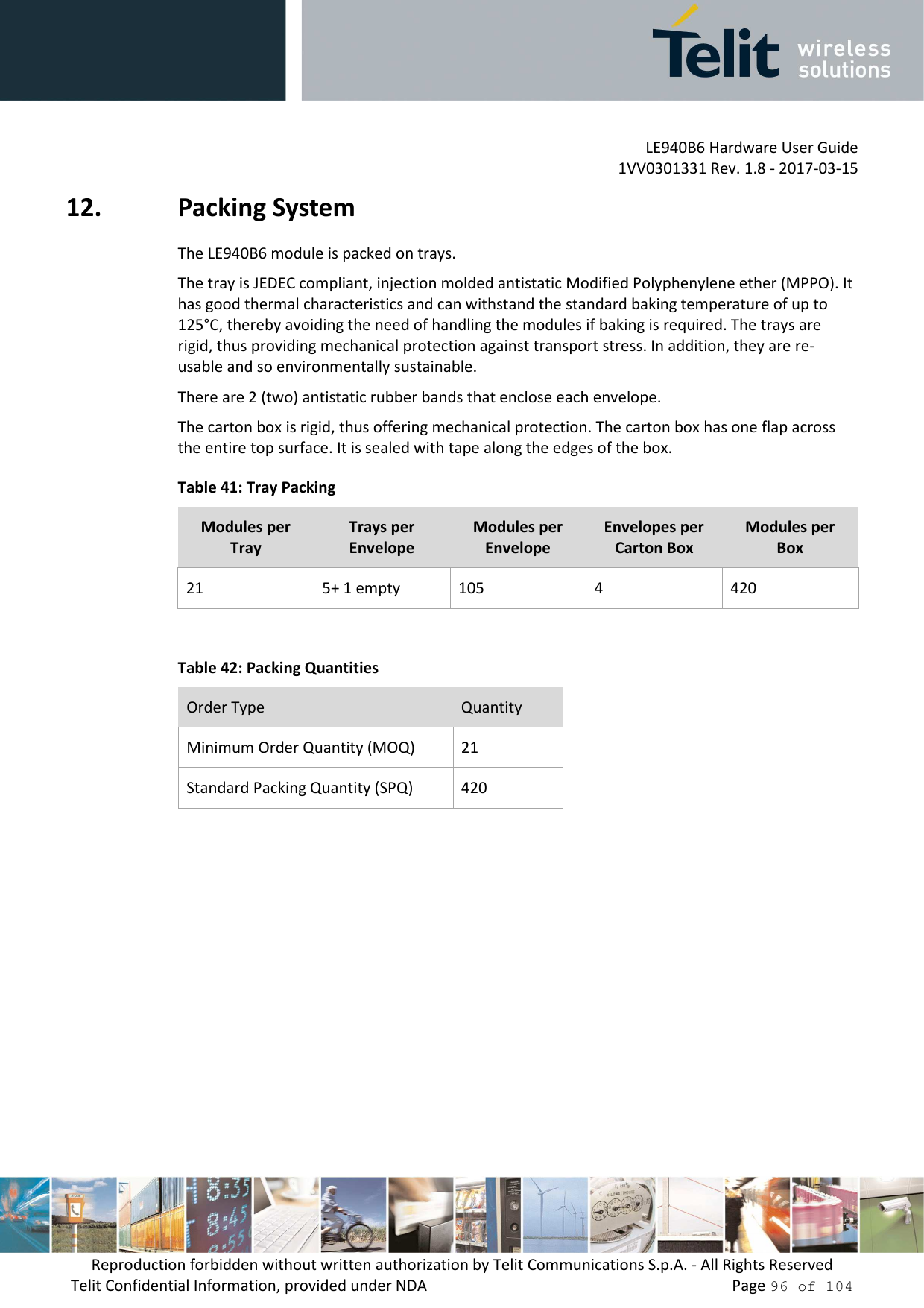
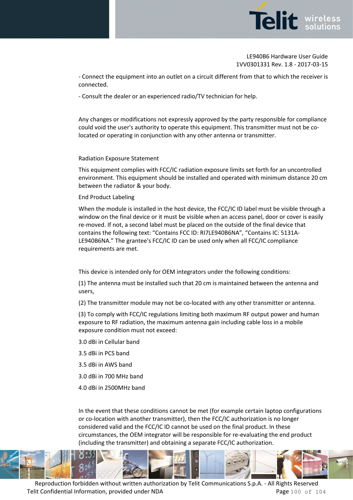
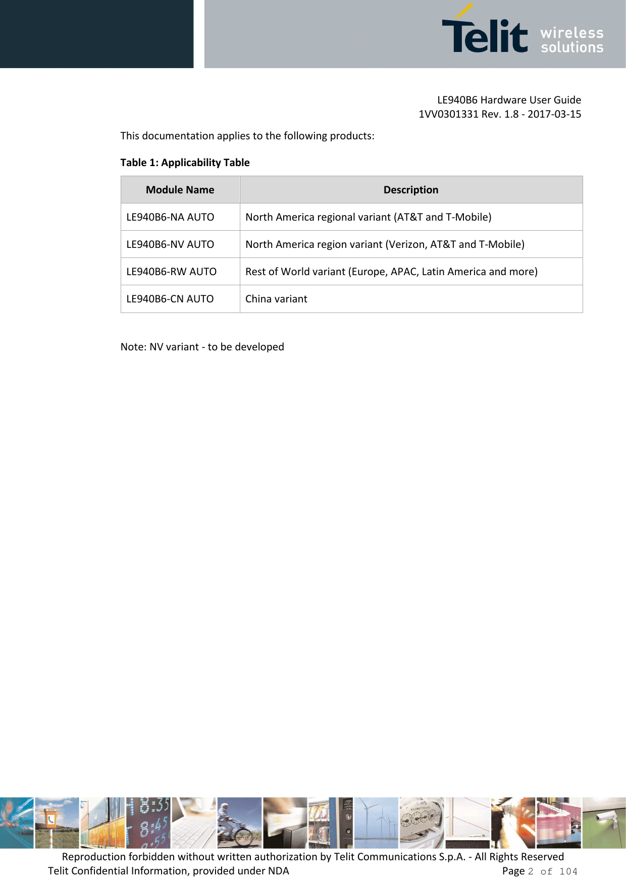
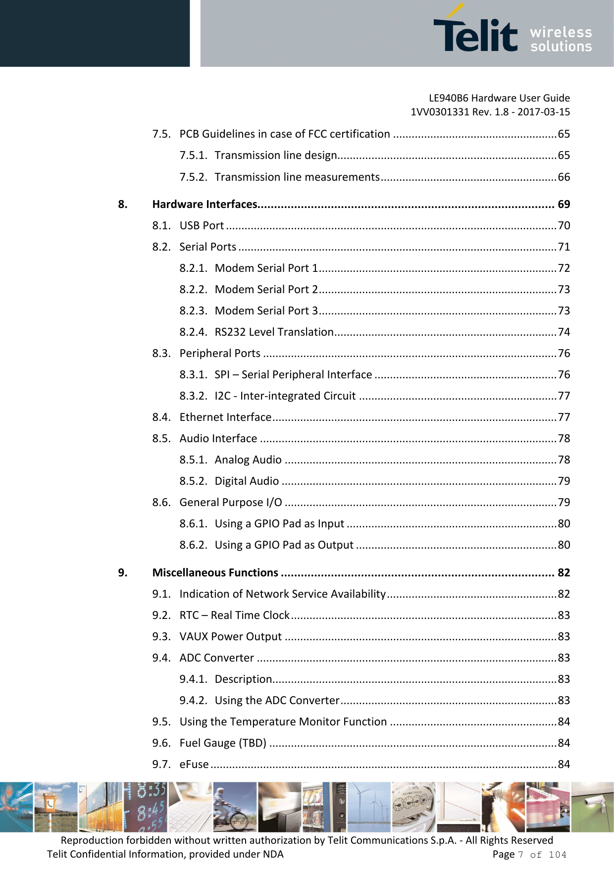
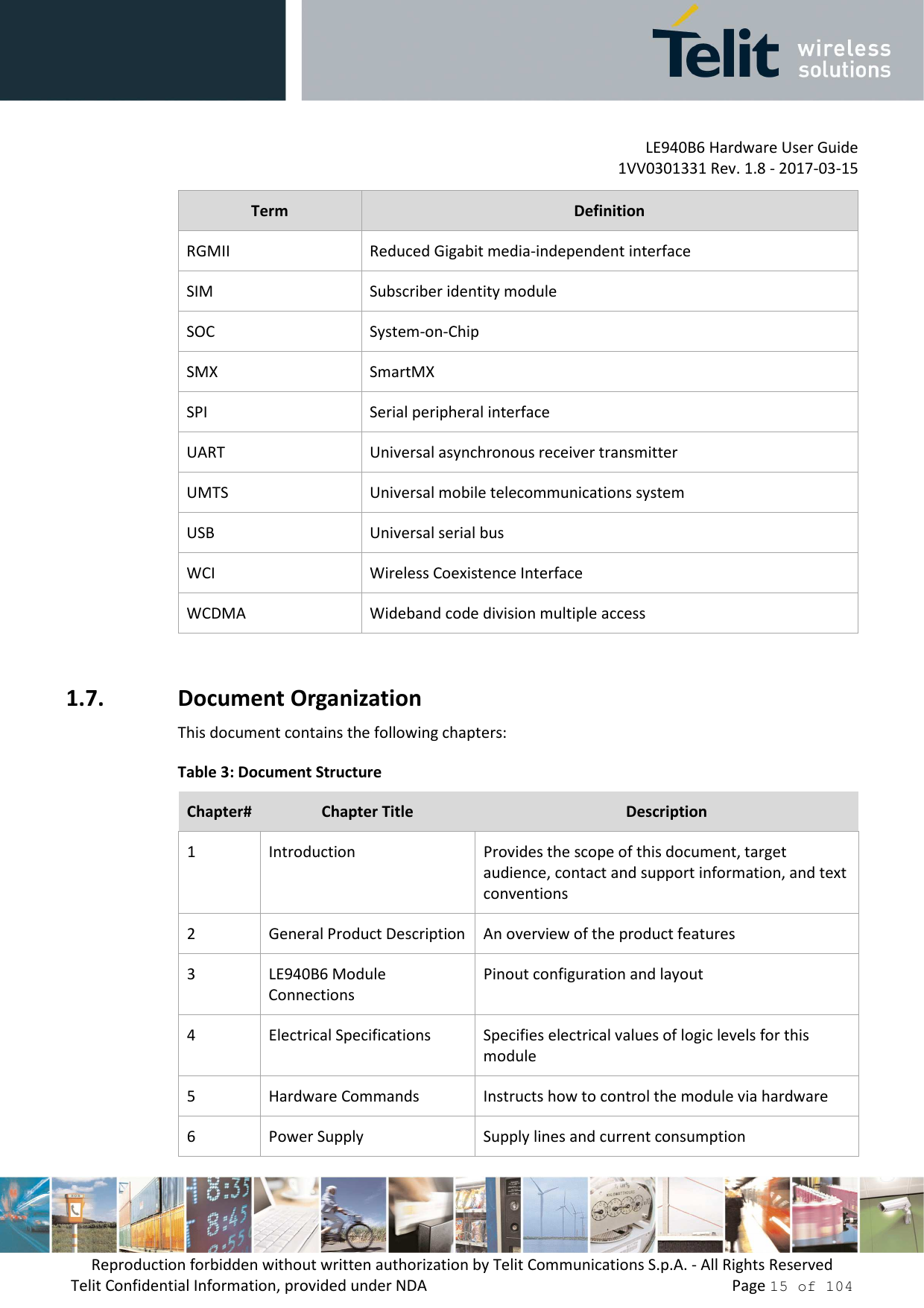
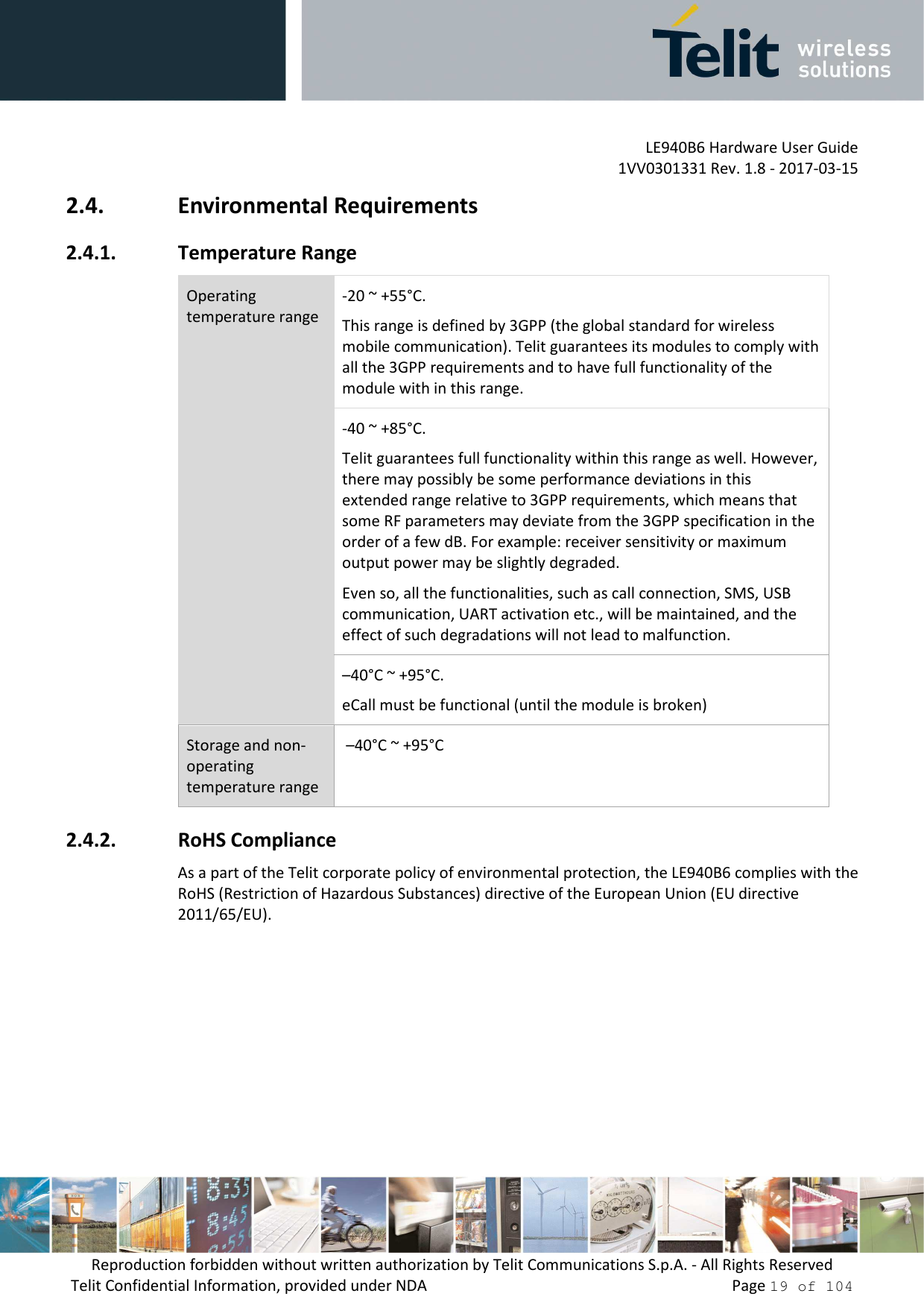
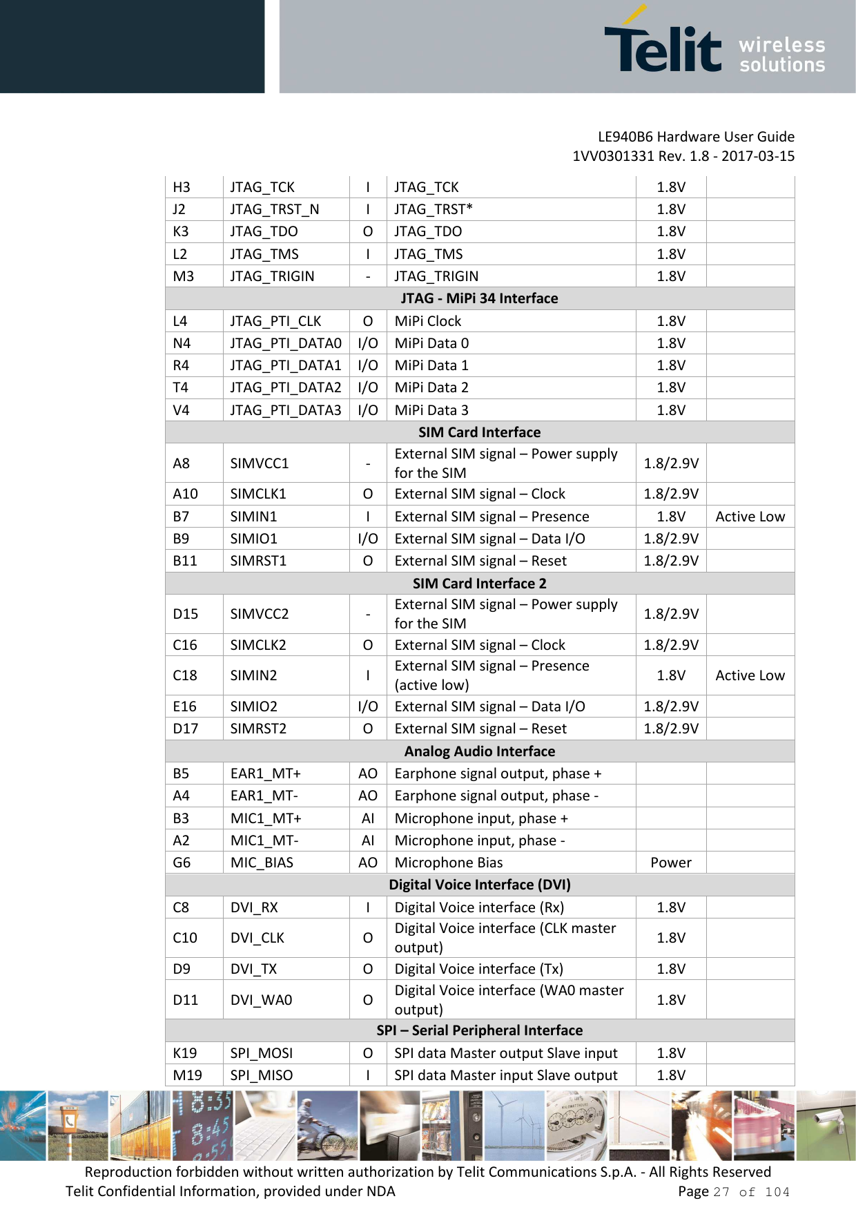
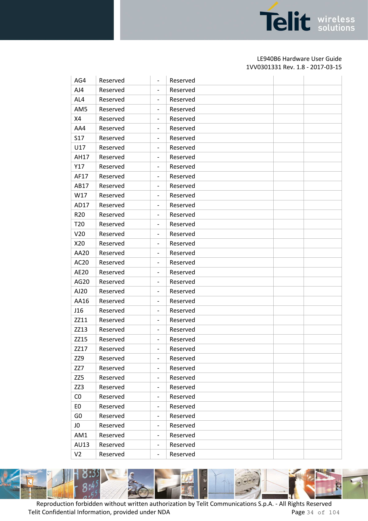
![LE940B6 Hardware User Guide 1VV0301331 Rev. 1.8 - 2017-03-15 Reproduction forbidden without written authorization by Telit Communications S.p.A. - All Rights Reserved Telit Confidential Information, provided under NDA Page 77 of 104 8.3.2. I2C - Inter-integrated Circuit The LE940B6 I2C is an alternate function of GPIO 1-15 pins. Available only from Modem side as SW emulation of I2C on GPIO lines. Any GPIO can be configured as SCL or SDA. LE940B6 supports I2C Master Mode only. NOTE: SW emulated I2C on GPIO lines is supported only from the modem side. For more information, refer to Ref 1: LE940B6 AT Command Reference Guide for command settings. 8.4. Ethernet Interface The LE940B6 has an integrated Ethernet interface to an external Ethernet PHY supporting 10M / 100M and 1G speed modes via a RGMII interface. The Ethernet interface is target to be compliant with the RGMII and RMII specifications. The supported RGMII and RMII specification versions are: • RGMII: Version 1.3, dated 12/10/2000, supporting up to 1000 Mbps operation • RMII: Version 1.2, dated 03/20/1998, supporting up to 100 Mbps operation NOTE: Customer should carefully design the Ethernet interface depending on PHY chipset; Please contact Telit R&D for more details and guidelines. Table 30: Ethernet Interface PAD Signal I/O Function Type COMMENT G14 MAC_MDC O Management Data Clock 2.5/3.3V G12 MAC_MDIO I/O Management Data I/O 2.5/3.3V V16 MAC_TXD[0] O RGMII or RMII TXD[0] 2.5/3.3V T16 MAC_TXD[1] O RGMII or RMII TXD[1] 2.5/3.3V R16 MAC_TXD[2] O RGMII TXD[2] 2.5/3.3V N16 MAC_TXD[3] O RGMII TXD[3] 2.5/3.3V L16 MAC_GTX_CLK O RGMII Transmit Clock 2.5/3.3V G16 MAC_TXEN_ER O RGMII Transmit Enable /Error or RMII Transmit Enable 2.5/3.3V](https://usermanual.wiki/Telit-Communications-S-p-A/LE940B6NA/User-Guide-3334482-Page-77.png)
![LE940B6 Hardware User Guide 1VV0301331 Rev. 1.8 - 2017-03-15 Reproduction forbidden without written authorization by Telit Communications S.p.A. - All Rights Reserved Telit Confidential Information, provided under NDA Page 78 of 104 PAD Signal I/O Function Type COMMENT AL16 MAC_RXD[0] I RGMII or RMII RXD[0] 2.5/3.3V AJ16 MAC_RXD[1] I RGMII or RMII RXD[1] 2.5/3.3V AG16 MAC_RXD[2] I RGMII RXD[2] 2.5/3.3V AE16 MAC_RXD[3] I RGMII RXD[3] 2.5/3.3V AC16 MAC_RX_CLK I RGMII Receive Clock 2.5/3.3V X16 MAC_RXDV_ER I RGMII Receive Data Available/Error or RMII Receive Error 2.5/3.3V G10 ETH_INT_N I Ethernet PHY Interrupt 2.5/3.3V G8 ETH_RST_N O Ethernet PHY Reset Output 2.5/3.3V 8.5. Audio Interface The LE940B6 module supports analog and digital audio interfaces. 8.5.1. Analog Audio The LE940B6 module provides an analog audio interface; a single differential input for the audio to be transmitted (Uplink), and a balanced output for the received audio (Downlink). The analog interface is on the following pins: Table 31: Analog Audio Signals PAD Signal I/O Function Type Comments B5 EAR1_MT+ AO Earphone signal output, phase + Audio A4 EAR1_MT- AO Earphone signal output, phase - Audio B3 MIC1_MT+ AI Microphone signal input, phase + Audio A2 MIC1_MT- AI Microphone signal input, phase - Audio G6 MICBIAS AO Microphone bias is 1.9~2.2V Power For more details, Application Note will be prepared for the Audio Settings.](https://usermanual.wiki/Telit-Communications-S-p-A/LE940B6NA/User-Guide-3334482-Page-78.png)