8devices JLP Broadband Digital Transmission System User Manual
8devices Broadband Digital Transmission System
8devices >
User manual
Jalapeno Data sheet
Quick specs
• 802.11 a/b/g/n/ac Wave 2, 2.4 and 5 GHz, 2x2
MIMO, 300 and 867 Mbps data rate, 23 dBm
per chain output power
• U.FL connectors for external an tenna
• 128 MB NAND and 8 MB NOR FLASH, 256 MB
DDR3 RAM
• Linux friendly , OpenWRT ash image and source
code are available for download on
www.8devices.com/wiki_jalapeno
• CPU – IPQ 4018 (700 MHz quad core Cortex A7)
• 23 dBm per chain output power dual-band
concurrent radio with dedicated Tensilica CPU
and 802.11ac Wave 2 support
• 32 by 47 mm size
• Surface mountable, dual-side design
• Available interfaces - USB 2.0, USB 3.0, I2S,
TDM, UART, GPIO, JTAG and 2 x 1000
Base-T Ethernet ports
Jalapeno is based on an IPQ4018 SoC from
Qualcomm, which is extremely powerful quad
core 700MHz CPU Cortex A7 CPU with NEON
(high-performance media engine), ideal for
routers, gateways and access points. It is a
surface mountable, dual-sided, Wi-Fi enabled
Linux module.
It comes with a high-power (23 dBm per chain)
dual-band concurrent radio supporting 802.11ac
Wave2 technology (2x2 MiMo) reaching 1.167
Gbps data rate. USB 3.0, USB 2.0, I2S, UART,
GPIO are the interfaces available on the module
together with two Gigabit Ethernet ports. SoC
has hardware NAT engine and high-end security
features like crypto engine, secure boot and
others.
OpenWRT linux distribution source code is
available on GitHub https://github.com/8devices
and is supported by our growing community on
http://www.8devices.com/community forum.
Jalapeno is a very powerful quad-core CPU based module with dual
band concurrent radio supporting 802.11ac Wave 2 technology
2
Jalapeno Data sheet v1.2-18-2-20
Block diagram
Module dimensions
JALAPENO
MODULE
IPQ4018
SOC
FRONT END
QCA8072
ETHERNET
PHY
NAND
128MB
MEMORY
NOR
8MB
MEMORY
DDR3
256MB
MEMORY
+3.3V
1000 Base-T ETH0
1000 Base-T ETH1
USB 2.0
USB 3.0
I2S
TDM
UART
GPIO
JTAG RF ANT 0
FRONT END
DIPLEXER
FRONT END
RF ANT 1
FRONT END
DIPLEXER

3
Jalapeno Data sheet v1.2-18-2-20
Radio characteristics
2.4 GHz
802.11AC
(20 MHz)
Data rate (Mbps) 14.4 28.9 43.3 57.8 86.7 115.6 130.3 144.4 173.3
Sensitivity (dBm) -93 -90 -88 -85 80 -76 -74 -72 -68
Output power (dBm) 22 20 19 19 18 18 18 17 17
2.4 GHz
802.11AC
(40 MHz)
Data rate (Mbps) 30 60 90 120 180 240 270 300 360 400
Sensitivity (dBm) -90 -88 -85 -82 -77 -73 -73 -70 -66 -64
Output power (dBm) 21 19 18 18 18 18 17 17 17 17
5 GHz
802.11AC
(20 MHz)
Data rate (Mbps) 14.4 28.9 43.3 57.8 86.7 115.6 130.3 144.4 173.3
Sensitivity (dBm) -92 -89 -86 -83 -80 -76 -74 -73 -68
Output power (dBm) 22 20 19 19 18 18 18 17 17
5 GHz
802.11AC
(40 MHz)
Data rate (Mbps) 30 60 90 120 180 240 270 300 360 400
Sensitivity (dBm) -89 -86 -84 -81 -78 -73 -72 -70 -66 -67
Output power (dBm) 21 19 18 18 18 18 17 17 17 17
5 GHz
802.11AC
(80 MHz)
Data rate (Mbps) 65 130 195 260 390 520 585 650 780 866.7
Sensitivity (dBm) -86 -83 -80 -77 -74 -70 -69 -67 -63 -61
Output power (dBm) 21 19 18 18 18 18 17 17 17 17
Scenario Voltage, V Current, A Power, W
Idle without beacons 5 0.41 2.05
Idle with beacons 5 0.68 3.4
MCS0 HT20 5 2.55 12.75
MCS9 VHT80/HT40 (Highest rates) 5 1.78 8.9
Power consumption
Operating conditions
The module can operate in a wide temperature range and dierent conditions depending on the enclosure. The following
guidelines guarantee that it will work correctly.
Parameter Units Min Max
Working environment °C 0 55
Storage environment °C -40 70
Humidity %RH 10 90
Storage humidity %RH 5 90
Heatsink size recommendations
It is essetial to use heatsink for the hardware designs based on Jalapeno module. Heatsink should be able to dissipate 7W
and the recommended area is 175 cm2. It should be directly attached to the bottom side of Jalapeno module.
4
Jalapeno Data sheet v1.2-18-2-20
Module pinout
GND
1
ETH1_TRX0+
2
ETH1_TRX0-
3
ETH1_TRX1+
4
ETH1_TRX1-
5
ETH1_TRX2+
6
ETH1_TRX2-
7
ETH1_TRX3+
8
ETH1_TRX3-
9
GND
10
USB2_DM
11
USB2_DP
12
GND
13
USB3_SS_TX+
14
USB3_SS_TX-
15
GND
16
USB3_SS_RX+
17
USB3_SS_RX-
18
GND
19
USB3_HS_DM
20
USB3_HS_DP
21
GND
22
3.3V
23
GND
56
N.C.
55
GND
54
GND
53
N.C.
52
GND
51
GND
50
3.3V
49
N.C.
48
GND
47
RESET
46
GND
45
JTAG_TRST/ GPIO_5
44
JTAG_RST/ GPIO_4
43
JTAG_TDO/ GPIO_3
42
GND
41
JTAG_TMS
40
JTAG_TDI/ GPIO_0
39
JTAG_TCK/ GPIO_1
38
GND
37
3.3V
36
GPIO_58
24
GPIO_63
25
UART_RX/ GPIO_60
26
UART_TX/ GPIO_61
27
GND
28
GND
29
GND
30
GND
31
GND
32
GND
33
GND
34
GND
35
3.3V
57
GND
58
ETH0_100_LED
59
ETH1_100_LED
60
ETH0_1000_LED
61
ETH1_1000_LED
62
ETH0_TRX0+
63
ETH0_TRX0-
64
ETH0_TRX1+
65
ETH0_TRX1-
66
ETH0_TRX2+
67
ETH0_TRX2-
68
ETH0_TRX3+
69
ETH0_TRX3-
70
5
Jalapeno Data sheet v1.2-18-2-20
Pin Name GPIO function
select
Congurable
function
Voltage (V) Type Description
1 GND - - - - Ground connection
2 ETH1_TRX0+ - - - AI, AO 1000 Base-T output positive
3 ETH1_TRX0- - - - AI, AO 1000 Base-T output negative
4 ETH1_TRX1+ - - - AI, AO 1000 Base-T output positive
5 ETH1_TRX1- - - - AI, AO 1000 Base-T output negative
6 ETH1_TRX2+ - - - AI, AO 1000 Base-T output positive
7 ETH1_TRX2- - - - AI, AO 1000 Base-T output negative
8 ETH1_TRX3+ - - - AI, AO 1000 Base-T output positive
9 ETH1_TRX3- - - - AI, AO 1000 Base-T output negative
10 GND - - - - Ground connection
11 USB2_DM - - - AI, AO USB 2.0 data negative
12 USB2_DP - - - AI, AO USB 2.0 data positive
13 GND - - - - Ground connection
14 USB3_SS_TX+ - - - AO USB 3.0 SuperSpeed transmitter positive
15 USB3_SS_TX- - - - AO USB 3.0 SuperSpeed transmitter negative
16 GND - - - - Ground connection
17 USB3_SS_RX+ - - - AI USB 3.0 SuperSpeed receiver positive
18 USB3_SS_RX- - - - AI USB 3.0 SuperSpeed receiver negative
19 GND - - - - Ground connection
20 USB3_HS_DM - - - AI, AO USB 2.0 data negative
21 USB3_HS_DP - - - AI, AO USB 2.0 data positive
22 GND - - - - Ground connection
23 3.3V - - - PI 3.3V power supply
24 GPIO58 0 GPIO 3.3 - -
2 LED[2] 3.3 O -
5 smart_ant6 3.3 IO -
25 GPIO63 0 GPIO 3.3 - -
5 Audio_txd[1] 3.3 O Audio transmit data
6 Audio_rxd 3.3 I Audio receive data
26 UART_RX/GPIO60 0 GPIO 3.3 - -
2 blsp_uart0_rxd(1) 3.3 I UART RX
4 smart_ant4 3.3 IO -
5 LED[0] 3.3 O -
6 audio_txbclk 3.3 IO Audio transmit bit block
7 audio_rxbclk 3.3 IO Audio receive bit block
27 UART_TX/GPIO61 0 GPIO 3.3 - -
2 blsp_uart0_txd 3.3 O UART TX
4 smart_ant5 3.3 IO -
5 audio_txfsync 3.3 IO Audio transmit frame sync
6 audio_rxfsync 3.3 IO Audio receiver frame sync
7 LED[1] 3.3 O -
boot_cong(14) 3.3 I -
6
Jalapeno Data sheet v1.2-18-2-20
Pin Name GPIO function
select
Congurable
function
Voltage (V) Type Description
28 GND - - - - Ground connection
29 GND - - - - Ground connection
30 GND - - - - Ground connection
31 GND - - - - Ground connection
32 GND - - - - Ground connection
33 GND - - - - Ground connection
34 GND - - - - Ground connection
35 GND - - - - Ground connection
36 3.3V - - - PI 3.3V power supply
37 GND - - - - Ground connection
38 JTAG_TCK/GPIO1 0 GPIO 3.3 - -
1 JTAG_TCK 3.3 I JTAG test clock
39 JTAG_TDI/GPIO0 0 GPIO 3.3 - -
1 JTAG_TDI 3.3 I JTAG test data in
40 JTAG_TMS 0 GPIO 3.3 - -
1 JTAG_TMS 3.3 I JTAG test mode state
41 GND - - - - Ground connection
42 JTAG_TDO/GPIO3 0 GPIO 3.3 - -
1 JTAG_TDO 3.3 O JTAG test data out
- boot_con-
g(0)
3.3 I -
43 JTAG_RST_N/GPIO4 0 GPIO 3.3 - -
1 JTAG_RST_N 3.3 I JTAG reset for debug
44 JTAG_TRST_N/
GPIO5
0 GPIO 3.3 - -
1 JTAG_
TRST_N
3.3 I JTAG test reset
45 GND - - - - Ground connection
46 Reset - Module reset I 0 - reset, 1 - run
47 GND - - - - Ground connection
48 NC - - - - Not connected
49 3.3V - - - PI 3.3V power supply
50 GND - - - - Ground connection
51 GND - - - - Ground connection
52 NC - - - - Not connected
53 GND - - - - Ground connection
54 GND - - - - Ground connection
55 NC - - - - Not connected
56 GND - - - - Ground connection
57 3.3V - - - PI 3.3V power supply
58 GND - - - - Ground connection
59 ETH0_100_LED - - - AO LED output for 100 Base-T activity
60 ETH1_100_LED - - - AO LED output for 100 Base-T activity
61 ETH0_1000_LED - - - AO LED output for 1000 Base-T activity
62 ETH1_1000_LED - - - AO LED output for 1000 Base-T activity

7
Jalapeno Data sheet v1.2-18-2-20
Pin Name GPIO function
select
Congurable
function
Voltage (V) Type Description
63 ETH0_TRX0+ - - - AI, AO 1000 Base-T output positive
64 ETH0_TRX0- - - - AI, AO 1000 Base-T output negative
65 ETH0_TRX1+ - - - AI, AO 1000 Base-T output positive
66 ETH0_TRX1- - - - AI, AO 1000 Base-T output negative
67 ETH0_TRX2+ - - - AI, AO 1000 Base-T output positive
68 ETH0_TRX2- - - - AI, AO 1000 Base-T output negative
69 ETH0_TRX3+ - - - AI, AO 1000 Base-T output positive
70 ETH0_TRX3- - - - AI, AO 1000 Base-T output negative
PI - Power input
IO - digital bi-directional signal
O - digital output
I - digital input
AO - analog output
AI - analog input
Power supply
It is recommended to use pin 23, 36, 49 and 57 to give power supply to the module.
Power ratings
Parameter Units Min Nominal Max
3.3V power supply V 3.13 3.3 3.46
Digital I/O characteristics for 3.3V I/O
Parameter Comments Min Max Units
VIH High-level input voltage CMOS/ Schmitt 2 3.6 V
VIL Low-level input voltage CMOS/ Schmitt -0.3 0.4 V
VSHYS Schmitt hysteresis voltage - – – mV
IIH Input high leakage current 11, 2 No pulldown – 1 μA
IIL Input low leakage current 1, 2 No pullup -1 – μA
IIHPD Input high leakage current 1, 3 With pulldown 10 60 μA
IILPU Input low leakage current 2, 3 With pullup -60 -10 μA
VOH High-level output voltage 4 CMOS, at pin-rated drive strength 3.0 3.6 V
VOL Low-level output voltage 4 CMOS, at pin-rated drive strength -0.3 0.4 V
IOZH Tri-state leakage current 1 Logic high output, no pulldown – 1 μA
IOZL Tri-state leakage current 2 Logic low output, no pullup -1 – μA
IOZHPD Tri-state leakage current 1, 3 Logic high output with pulldown 10 60 μA
IOZLPU Tri-state leakage current 2, 3 Logic low output with pullup -60 -10 μA
CIN Input capacitance 5- – 5 pF
Soware
OpenWRT linux distribution source code is available on GitHub https://github.com/8devices and is supported by our growing
community on http://www.8devices.com/community forum.
8
Jalapeno Data sheet v1.2-18-2-20
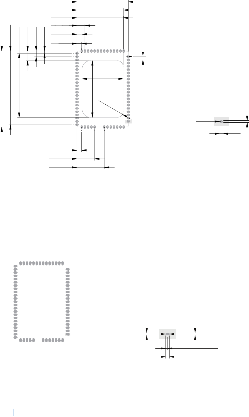
PCB footprint
25.5
35
5.95
39.5
R3.75
2.9
4.9
28.9
31.8
1.45
3.45
45.45
46.90
2.9
16.9
10.9
3.15
28.65
1.2
1.9
R0.6
Cut
A
Detail A
2
Soldering paste footprint
2.35
1.4
1.15
R0.6
R0.74
B
Detail B
1.2
9
Jalapeno Data sheet v1.2-18-2-20
Reflow profile recommendation
Ramp up rate 3°C/second max
Maximum time maintained above 217°C 120 seconds
Peak temperature 250°C
Maximum time within 5°C of peak temperature 20 seconds
Ramp down rate 6°C/second max
Reflow profile
Time
Temperature, C
250
200
150
100
50
0
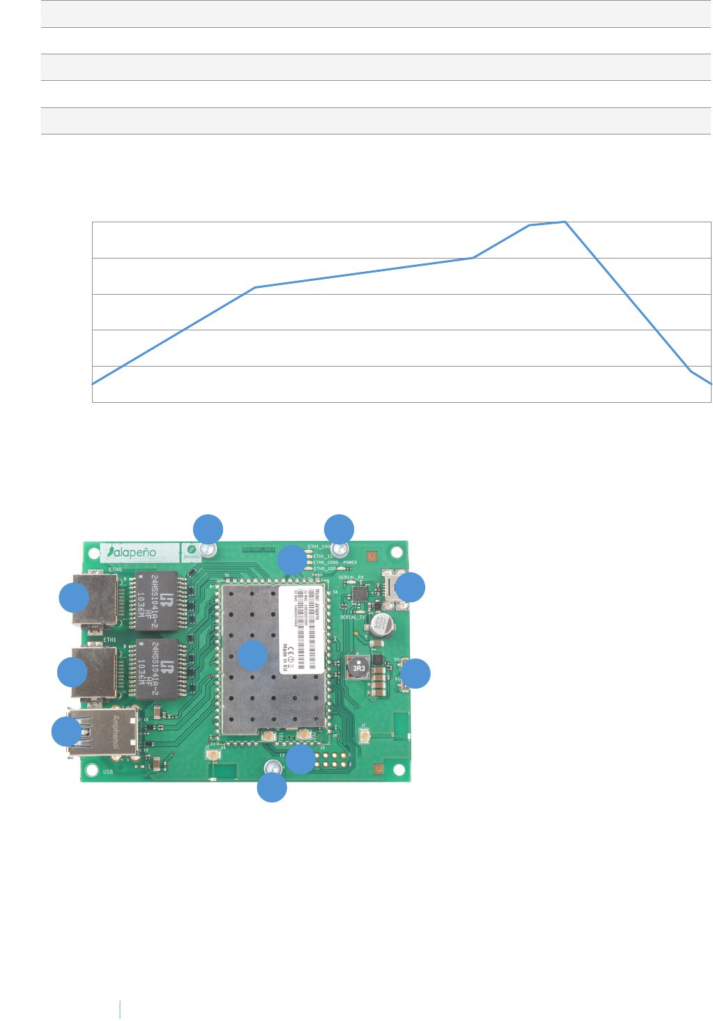
Development kit
1
2
3
4
5
6
1 - 2 x 1000 Base-T Ethernet ports
2 - 2 x USB Type-A sockets (2.0 and 3.0)
3 - Mini USB Type-A socket (console + power)
4 - Buttons (reset and user - GPIO connected)
5 - External LEDs
6 - 2.45 mm pitch prototyping are holes
7 - Heatsink mounting screws
8 - Jalapeno module
7 7
7
8
1
FCC Warning:
If the FCC identification number is not visible when the module is installed inside another device, then the outside of the device into
which the module is installed must also display a label referring to the enclosed module. This exterior label can use wording such as the
following: “Contains Transmitter Module FCC ID: Z9W-JLP”, when the module is installed inside another device, the user manual of
this device must contain below warning statements;
1. This device complies with Part 15 of the FCC Rules. Operation is subject to the following two conditions:
(1) This device may not cause harmful interference.
(2) This device must accept any interference received, including interference that may cause undesired operation.
2. Changes or modifications not expressly approved by the party responsible for compliance could void the user's authority to operate
the equipment.
NOTE:
This equipment has been tested and found to comply with the limits for a Class B digital device, pursuant to Part 15 of the FCC Rules.
These limits are designed to provide reasonable protection against harmful interference in a residential installation.
This equipment generates uses and can radiate radio frequency energy and, if not installed and used in accordance with the
instructions, may cause harmful interference to radio communications. However, there is no guarantee that interference will not occur
in a particular installation. If this equipment does cause harmful interference to radio or television reception, which can be determined
by turning the equipment off and on, the user is encouraged to try to correct the interference by one or more of the following measures:
-Reorient or relocate the receiving antenna.
-Increase the separation between the equipment and receiver.
-Connect the equipment into an outlet on a circuit different from that to which the receiver is connected.
-Consult the dealer or an experienced radio/TV technician for help.
This modular complies with FCC RF radiation exposure limits for an uncontrolled environment. This transmitter must not be co-located
or operating in conjunction with any other antenna or transmitter. This modular must be installed and operated with a minimum distance
of 20 cm between the radiator and user body.
The device indoor use only for 5150MHz~5250MHz.
This device complies with part 15 of the FCC Rules. Operation is subject to the following two conditions:
(1) This device may not cause harmful interference, and
(2) this device must accept any interference received, including interference that may cause undesired operation.
Changes or modifications not expressly approved by the party responsible for compliance could void the user's authority
to operate the equipment
IC Warning:
This device complies with Industry Canada’s licence-exempt RSSs. Operation is subject to the following two conditions:
(1) This device may not cause interference; and
(2) This device must accept any interference, including interference that may cause undesired operation of the device.
Cet appareil est conforme aux CNR exemptes de licence d'Industrie Canada . Son fonctionnement est soumis aux deux conditions
suivantes :
( 1 ) Ce dispositif ne peut causer d'interférences ; et
( 2 ) Ce dispositif doit accepter toute interférence , y compris les interférences qui peuvent causer un mauvais fonctionnement de
l'appareil.
This modular complies with IC RF radiation exposure limits set forth for an uncontrolled environment. This transmitter must not be
co-located or operating in conjunction with any other antenna or transmitter.
If the IC number is not visible when the module is installed inside another device, then the outside of the device into which the module
is installed must also display a label referring to the enclosed module. This exterior label can use wording such as the following:
“Contains IC: 11468A-JLP”
when the module is installed inside another device, the user manual of this device must contain below warning statements;
1. This device complies with Industry Canada’s licence-exempt RSSs. Operation is subject to the following two conditions:
(1) This device may not cause interference; and
(2) This device must accept any interference, including interference that may cause undesired operation of the device.
2. Cet appareil est conforme aux CNR exemptes de licence d'Industrie Canada . Son fonctionnement est soumis aux deux conditions
suivantes :
( 1 ) Ce dispositif ne peut causer d'interférences ; et
( 2 ) Ce dispositif doit accepter toute interférence , y compris les interférences qui peuvent causer un mauvais fonctionnement de
l'appareil.
The devices must be installed and used in strict accordance with the manufacturer's instructions as described in the user
documentation that comes with the product
This modular complies with FCC RF radiation exposure limits for an uncontrolled environment. This transmitter must not be co-located
or operating in conjunction with any other antenna or transmitter. This modular must be installed and operated with a minimum distance
of 20 cm between the radiator and user body.
The device indoor use only for 5150MHz~5250MHz.
Approved antenna:
Antenna Type: Antenna 0: Ceramic Antenna, Antenna 1: Omni Antenna
Antenna gain: Antenna 0: 3dBi, Antenna 1: 10dBi
Manufacture: TDK