ADC Telecommunications DCX8001A Digivance® CXD 800 MHz A Band User Manual Cover D
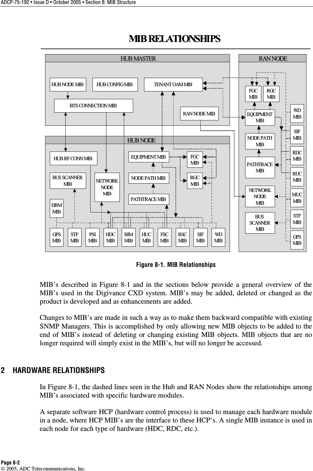
ADC Telecommunications Inc Digivance® CXD 800 MHz A Band Cover D
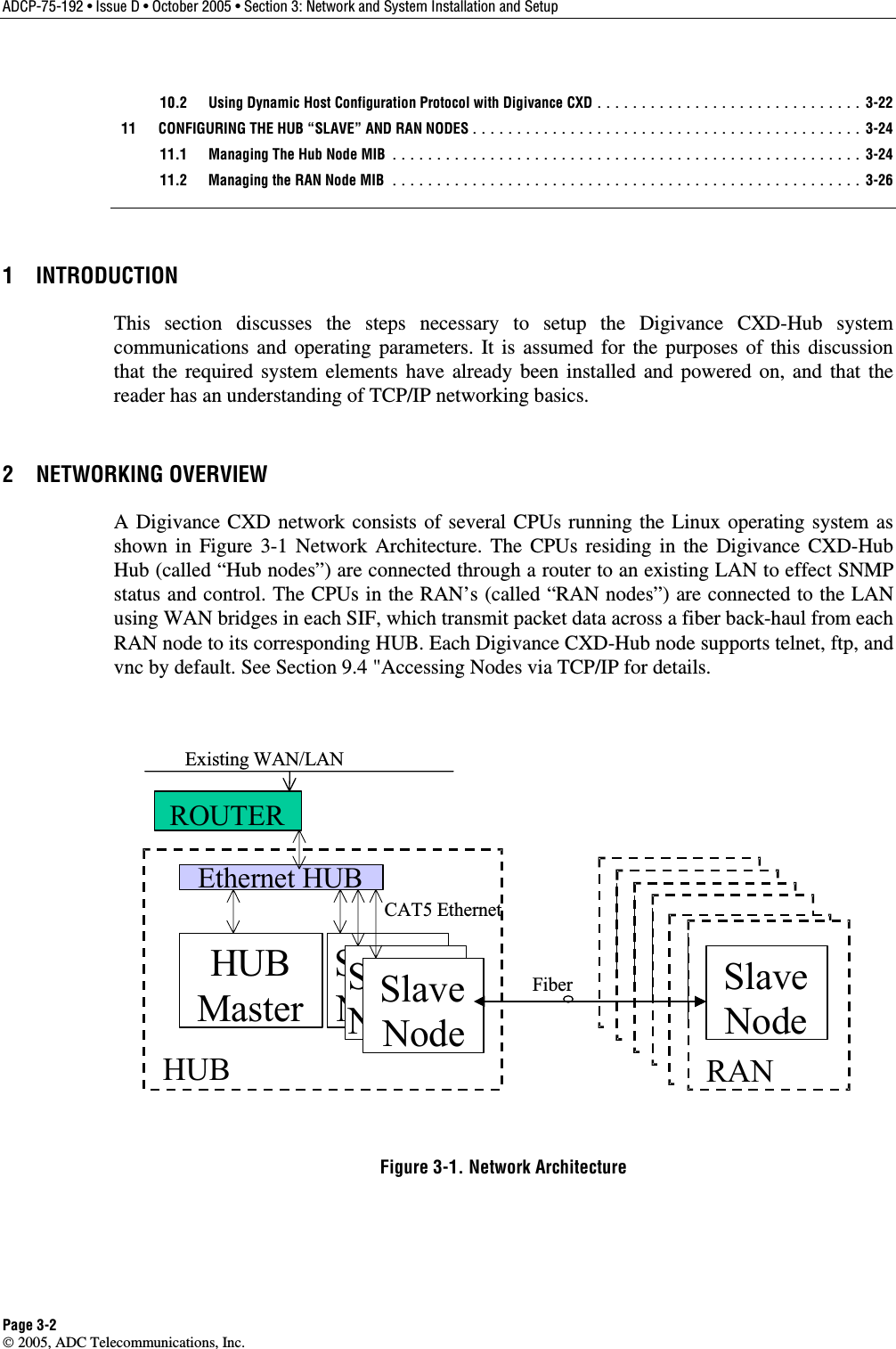
UserManual.wiki
>
ADC Telecommunications
>
DCX8001A User Manual
Manual
Navigation menu
Upload a User Manual
Namespaces
Wiki Guide
HTML
PDF
Info
Views
User Manual
Discussion / Help
Navigation
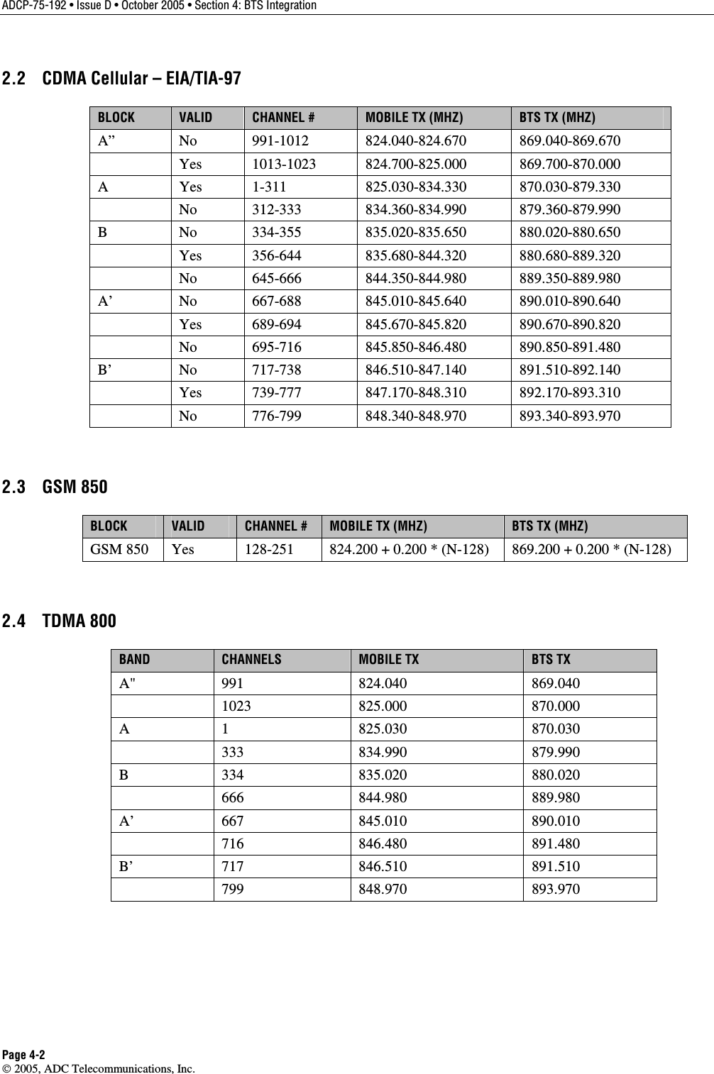
![ADCP-75-192 • Issue D • October 2005 • Section 3: Network and System Installation and Setup Page 3-17 2005, ADC Telecommunications, Inc. 8 MANAGING THE TENANT OAM ADDRESS AND HOSTNAME TABLES Within the Tenant OAM MIB, there are two (2) tables used to capture the current IP Addresses and Hostnames of all CPUs that are associated with a given tenant sector. The ordering of the CPUs in the MIB tables is such that the RAN CPUs are listed first from 1-8, followed by the Hub CPUs. The RAN ordering from 1-8 is important so that the RAN CPUs can be correlated to the RAN ID values used throughout the Tenant OAM MIB. 8.1 RAN Ordering The IP Address and Hostname tables in the Tenant OAM MIB indicate which RAN, based on IP address and hostname, corresponds to RAN X, where X is the RAN ID (1-8). Tenant processing uses a least-recently-used scheme to determine the RAN ID to assign to newly discovered RAN’s. When Tenant processing discovers new RAN’s that contain hardware associated with that tenant (based on Tenant ID of pathtrace string), the new RAN is assigned the next sequential "never-been-used" RAN ID, a value from 1-8. If there are no RAN IDs that have never been used, then Tenant processing will find the least-recently-used RAN ID and assign that ID to the newly discovered RAN. The RAN ID is important because it lets the user of the Tenant OAM MIB determine which RAN corresponds to the RAN-specific MIB parameters, such as: TenantRanDisableX, TenantRanXForwardMeasuredGain and TenantRanForwardGainOffsetX where X is the RAN ID, a value from 1-8. The RAN ID assignments will be persistently maintained through resets of the Hub Master CPU and other CPUs in the network, which will allow the NMS to program the RAN IDs when new RAN’s are added to the tenant simulcast group. In the future, the RAN ID assignments will not be persistent through resets of the network nodes, which will require that the NMS automatically correlate RAN ID to RAN CPU relationships. 8.2 Bracketing of Lost RAN’s When a RAN CPU is removed from the network, or if Tenant processing is unable to communicate with one of its RANs, then that RAN ID in the Hostname table is bracketed. For example hostname would be reported as [hostname]. In addition, the RAN ID in the Address table is also reported in a different fashion when a RAN is "lost". The IP address is bracketed, with the IP address string being replaced by another form of the number. For example, 172.20.1.248 could be replaced by [1921681.248]. The point is that if the IP address reported in the Address table is not a valid combination of 4 octet values with decimal points separating the octets, then that RAN should be considered not present.](https://usermanual.wiki/ADC-Telecommunications/DCX8001A/User-Guide-598656-Page-75.png)