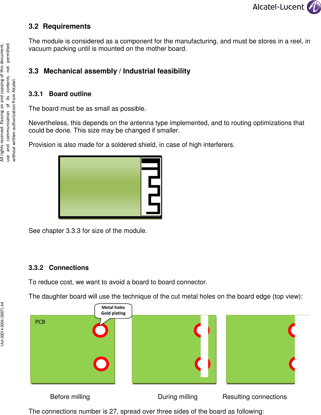
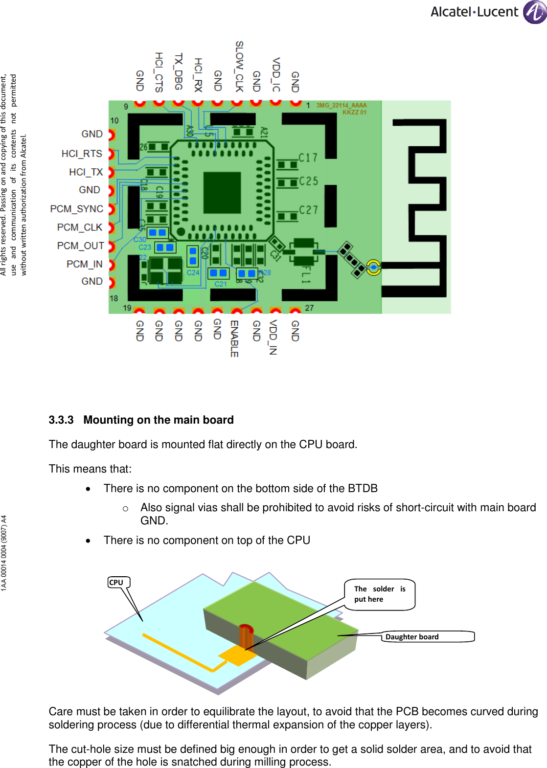
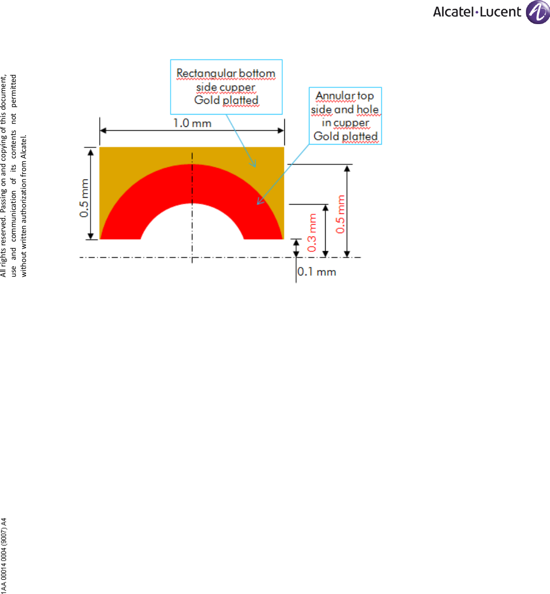
ALE BTMOD01 Bluetooth Daughter Board User Manual
Alcatel-Lucent Enterprise Bluetooth Daughter Board Users Manual
UserManual.wiki
>
ALE
>
BTMOD01 User Manual
Users Manual
Navigation menu
Upload a User Manual
Namespaces
Wiki Guide
HTML
PDF
Info
Views
User Manual
Discussion / Help
Navigation
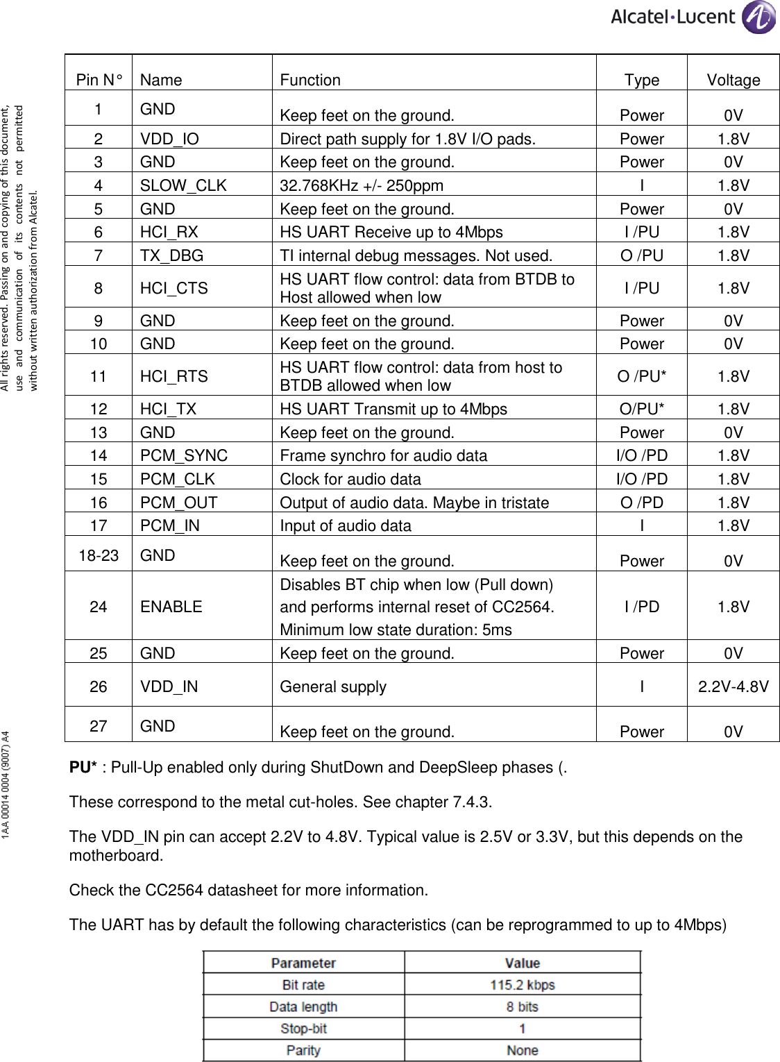
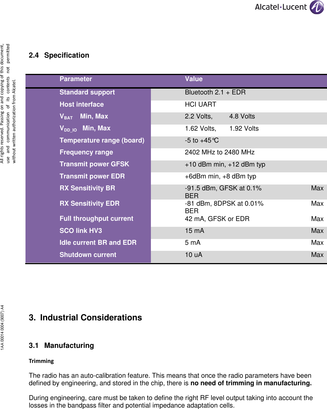
![All rights reserved. Passing on and copying of this document, use and communication of its contents not permitted without written authorization from Alcatel. 1. Generalities 1.1 Introduction 1.1.1 Overview The main objectives for this board, discussed also with the marketing are: Get lowest cost solution to enable BT for a maximum of IP terminals Enable new usages like o The phone is seen as a carkit for a smartphone o The phone can exchange phonebook with a smartphone From R&D point of view: o The board must be small enough to be integrated easily into our ID. o The board must integrate the antenna to avoid a re-certification for each phone which would use it. For this project, a pre-study has been done. See reference [1]. The choice is to do a daughter board with the chip CC2564 from Texas Instruments, with an integrated antenna on the layout (Printed antenna). 1.1.2 Aim of the document A pre-study has been done, in order to define the best choices for the whole solution, going from antenna to the BT management software in the phone. This document is intended to give all the technical inputs in order to make a BT daughter board which will be used on the Alcatel-Lucent IP Phones. A first step will be to use it on 8088, but we should care to make it possible to be used also on nextgen phones. 1.2 Services provided by the feature or equipment The BTDB will give a BT2.1+ EDR connectivity to the product where it is mounted into. The main reasons of this daughter board are to have: A common function usable on several phones without the need of RF expertise and full BT qualification A cost effective solution 1.3 External Interfaces The interface signals are listed hereafter:](https://usermanual.wiki/ALE/BTMOD01/User-Guide-2550347-Page-2.png)