ALE BTMOD01 Bluetooth Daughter Board User Manual
Alcatel-Lucent Enterprise Bluetooth Daughter Board Users Manual
ALE >
Users Manual

All rights reserved. Passing on and copying of this document,
use and communication of its contents not permitted
without written authorization from Alcatel.
Table of Content
1. GENERALITIES ................................................................................................................... 2
1.1 INTRODUCTION ............................................................................................................................................. 2
1.1.1 Overview .................................................................................................................................................. 2
1.1.2 Aim of the document ................................................................................................................................. 2
1.2 SERVICES PROVIDED BY THE FEATURE OR EQUIPMENT ................................................................................. 2
1.3 EXTERNAL INTERFACES ................................................................................................................................ 2
1.4 TERMINOLOGY / ABBREVIATIONS ................................................................................................................. 4
2. GENERAL DESCRIPTION ................................................................................................. 5
2.1 BT FUNCTION GLOBAL LOGICAL BLOC DIAGRAM ......................................................................................... 5
2.2 BT DAUGHTER BOARD BLOC DIAGRAM ........................................................................................................ 5
2.3 MECHANICAL ASPECTS AND INTEGRATION ................................................................................................... 6
2.4 SPECIFICATION .............................................................................................................................................. 7
3. INDUSTRIAL CONSIDERATIONS ................................................................................... 7
3.1 MANUFACTURING ......................................................................................................................................... 7
3.2 REQUIREMENTS ............................................................................................................................................ 8
3.3 MECHANICAL ASSEMBLY / INDUSTRIAL FEASIBILITY .................................................................................... 8
3.3.1 Board outline ............................................................................................................................................ 8
3.3.2 Connections.............................................................................................................................................. 8
3.3.3 Mounting on the main board .................................................................................................................... 9
3.3.4 Shielding Mounting ................................................................................................................................ 11
4. REGULATORY COMPLIANCE ....................................................................................... 12
4.1 FCC STATEMENT: ........................................................................................................................................ 12
4.2 IC STATEMENT: ........................................................................................................................................... 12

All rights reserved. Passing on and copying of this document,
use and communication of its contents not permitted
without written authorization from Alcatel.
1. Generalities
1.1 Introduction
1.1.1 Overview
The main objectives for this board, discussed also with the marketing are:
Get lowest cost solution to enable BT for a maximum of IP terminals
Enable new usages like
o The phone is seen as a carkit for a smartphone
o The phone can exchange phonebook with a smartphone
From R&D point of view:
o The board must be small enough to be integrated easily into our ID.
o The board must integrate the antenna to avoid a re-certification for each phone
which would use it.
For this project, a pre-study has been done. See reference [1].
The choice is to do a daughter board with the chip CC2564 from Texas Instruments, with an
integrated antenna on the layout (Printed antenna).
1.1.2 Aim of the document
A pre-study has been done, in order to define the best choices for the whole solution, going from
antenna to the BT management software in the phone.
This document is intended to give all the technical inputs in order to make a BT daughter board
which will be used on the Alcatel-Lucent IP Phones.
A first step will be to use it on 8088, but we should care to make it possible to be used also on
nextgen phones.
1.2 Services provided by the feature or equipment
The BTDB will give a BT2.1+ EDR connectivity to the product where it is mounted into. The main
reasons of this daughter board are to have:
A common function usable on several phones without the need of RF expertise and full
BT qualification
A cost effective solution
1.3 External Interfaces
The interface signals are listed hereafter:
All rights reserved. Passing on and copying of this document,
use and communication of its contents not permitted
without written authorization from Alcatel.
Pin N°
Name
Function
Type
Voltage
1
GND
Keep feet on the ground.
Power
0V
2
VDD_IO
Direct path supply for 1.8V I/O pads.
Power
1.8V
3
GND
Keep feet on the ground.
Power
0V
4
SLOW_CLK
32.768KHz +/- 250ppm
I
1.8V
5
GND
Keep feet on the ground.
Power
0V
6
HCI_RX
HS UART Receive up to 4Mbps
I /PU
1.8V
7
TX_DBG
TI internal debug messages. Not used.
O /PU
1.8V
8
HCI_CTS
HS UART flow control: data from BTDB to
Host allowed when low
I /PU
1.8V
9
GND
Keep feet on the ground.
Power
0V
10
GND
Keep feet on the ground.
Power
0V
11
HCI_RTS
HS UART flow control: data from host to
BTDB allowed when low
O /PU*
1.8V
12
HCI_TX
HS UART Transmit up to 4Mbps
O/PU*
1.8V
13
GND
Keep feet on the ground.
Power
0V
14
PCM_SYNC
Frame synchro for audio data
I/O /PD
1.8V
15
PCM_CLK
Clock for audio data
I/O /PD
1.8V
16
PCM_OUT
Output of audio data. Maybe in tristate
O /PD
1.8V
17
PCM_IN
Input of audio data
I
1.8V
18-23
GND
Keep feet on the ground.
Power
0V
24
ENABLE
Disables BT chip when low (Pull down)
and performs internal reset of CC2564.
Minimum low state duration: 5ms
I /PD
1.8V
25
GND
Keep feet on the ground.
Power
0V
26
VDD_IN
General supply
I
2.2V-4.8V
27
GND
Keep feet on the ground.
Power
0V
PU* : Pull-Up enabled only during ShutDown and DeepSleep phases (.
These correspond to the metal cut-holes. See chapter 7.4.3.
The VDD_IN pin can accept 2.2V to 4.8V. Typical value is 2.5V or 3.3V, but this depends on the
motherboard.
Check the CC2564 datasheet for more information.
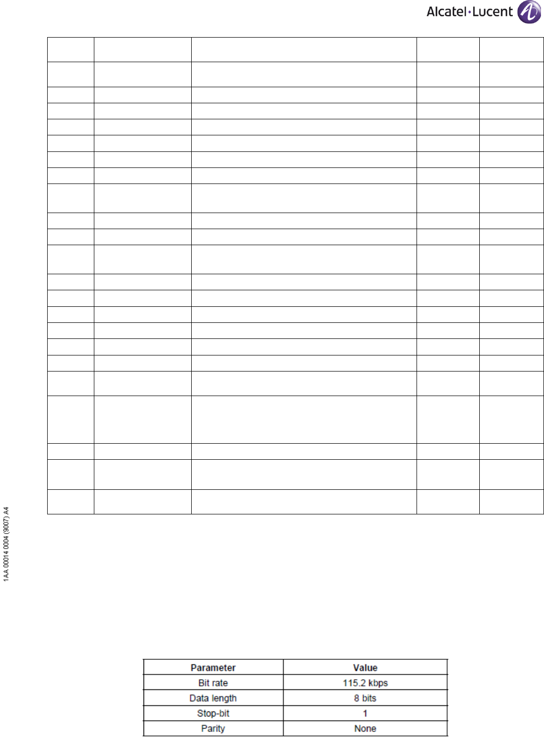
The UART has by default the following characteristics (can be reprogrammed to up to 4Mbps)
All rights reserved. Passing on and copying of this document,
use and communication of its contents not permitted
without written authorization from Alcatel.
Check the CC2564 datasheet for more information.
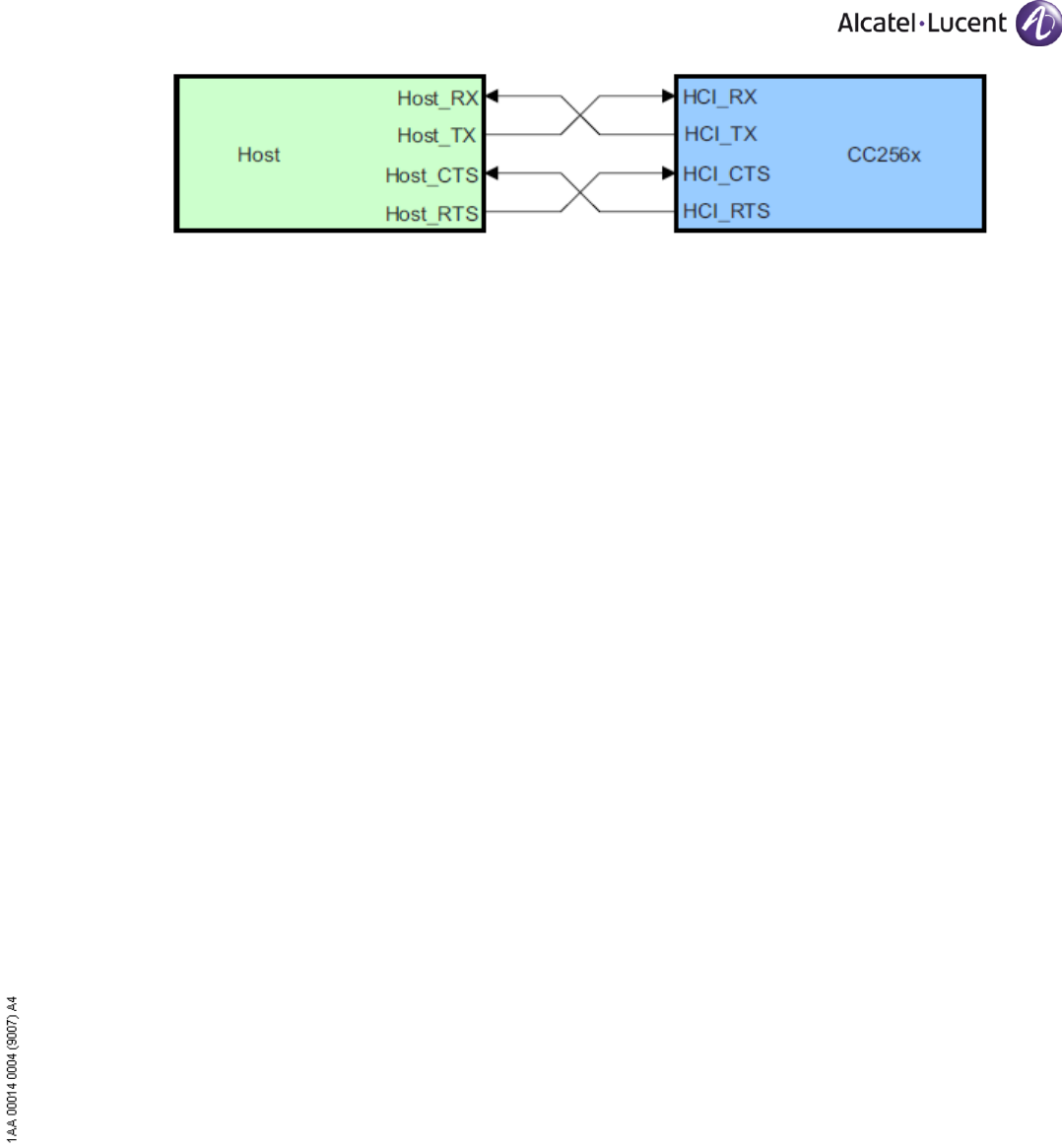
This cabling supposes that the Host is in DTE mode. In case of DCE host, RTS and CTS are
straight, and not crossed.
1.4 Terminology / Abbreviations
BTDB: BlueTooth Daughter Board
BT: BlueTooth
All rights reserved. Passing on and copying of this document,
use and communication of its contents not permitted
without written authorization from Alcatel.
2. General Description
2.1 BT function global logical bloc diagram
2.2 BT daughter board bloc diagram
Crystal
26MHz
Bandpass
filter
2.4GHz Antenna
VDD Vdd I/O LDO_out
UART
PCM/I2S
SlowClock
Enable TI CC2564B
32.768KHz
1.8V
< 20ppm
2.2V-4.8V
DC/DC
1.8V
UART
PCM
GPIO
Daughter Board PCB
All rights reserved. Passing on and copying of this document,
use and communication of its contents not permitted
without written authorization from Alcatel.
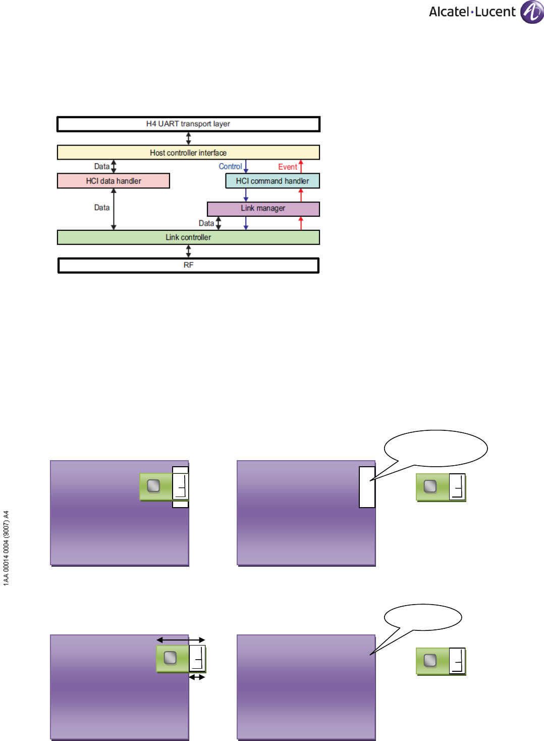
The CC2564 communicates with a standard HCI through the UART interface.
Here is a representation of the lower part of the stack, which is inside the CC2564:
This means that the upper part of the stack must be hosted in the mother board cpu.
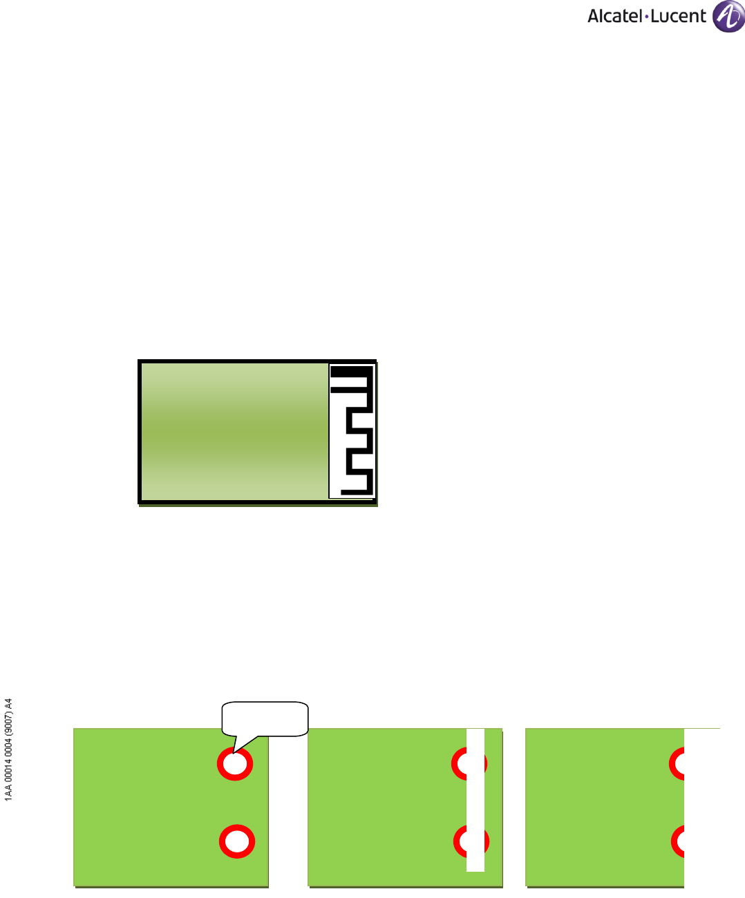
2.3 Mechanical aspects and integration
This board will be mounted on a IP Phone CPU board or BT handset CPU board.
For radiofrequency propagation reasons, the antenna area must not cover any copper plane.
For industrial reasons, the board must lay on the CPU board on at least 2/3 of it’s surface.
Examples of implementation follow:
= +
= +
Another alternative, best is:
= +
CPU PCB
CPU PCB
CPU PCB
Copper OK
CPU PCB
No copper under
antenna
L
L/3
max
All rights reserved. Passing on and copying of this document,
use and communication of its contents not permitted
without written authorization from Alcatel.
2.4 Specification
Parameter
Value
Standard support
Bluetooth 2.1 + EDR
Host interface
HCI UART
VBAT Min, Max
2.2 Volts, 4.8 Volts
VDD_IO Min, Max
1.62 Volts, 1.92 Volts
Temperature range (board)
-5 to +45°C
Frequency range
2402 MHz to 2480 MHz
Transmit power GFSK
+10 dBm min, +12 dBm typ
Transmit power EDR
+6dBm min, +8 dBm typ
RX Sensitivity BR
-91.5 dBm, GFSK at 0.1%
BER
Max
RX Sensitivity EDR
-81 dBm, 8DPSK at 0.01%
BER
Max
Full throughput current
42 mA, GFSK or EDR
Max
SCO link HV3
15 mA
Max
Idle current BR and EDR
5 mA
Max
Shutdown current
10 uA
Max
3. Industrial Considerations
3.1 Manufacturing
Trimming
The radio has an auto-calibration feature. This means that once the radio parameters have been
defined by engineering, and stored in the chip, there is no need of trimming in manufacturing.
During engineering, care must be taken to define the right RF level output taking into account the
losses in the bandpass filter and potential impedance adaptation cells.
All rights reserved. Passing on and copying of this document,
use and communication of its contents not permitted
without written authorization from Alcatel.
3.2 Requirements
The module is considered as a component for the manufacturing, and must be stores in a reel, in
vacuum packing until is mounted on the mother board.
3.3 Mechanical assembly / Industrial feasibility
3.3.1 Board outline
The board must be as small as possible.
Nevertheless, this depends on the antenna type implemented, and to routing optimizations that
could be done. This size may be changed if smaller.
Provision is also made for a soldered shield, in case of high interferers.
See chapter 3.3.3 for size of the module.
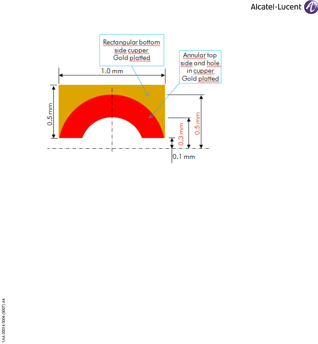
3.3.2 Connections
To reduce cost, we want to avoid a board to board connector.
The daughter board will use the technique of the cut metal holes on the board edge (top view):
Before milling During milling Resulting connections
The connections number is 27, spread over three sides of the board as following:
PCB
Metal holes
Gold plating
All rights reserved. Passing on and copying of this document,
use and communication of its contents not permitted
without written authorization from Alcatel.
3.3.3 Mounting on the main board
The daughter board is mounted flat directly on the CPU board.
This means that:
There is no component on the bottom side of the BTDB
o Also signal vias shall be prohibited to avoid risks of short-circuit with main board
GND.
There is no component on top of the CPU
Care must be taken in order to equilibrate the layout, to avoid that the PCB becomes curved during
soldering process (due to differential thermal expansion of the copper layers).
The cut-hole size must be defined big enough in order to get a solid solder area, and to avoid that
the copper of the hole is snatched during milling process.
The solder is
put here
CPU
Daughter board
All rights reserved. Passing on and copying of this document,
use and communication of its contents not permitted
without written authorization from Alcatel.
All rights reserved. Passing on and copying of this document,
use and communication of its contents not permitted
without written authorization from Alcatel.
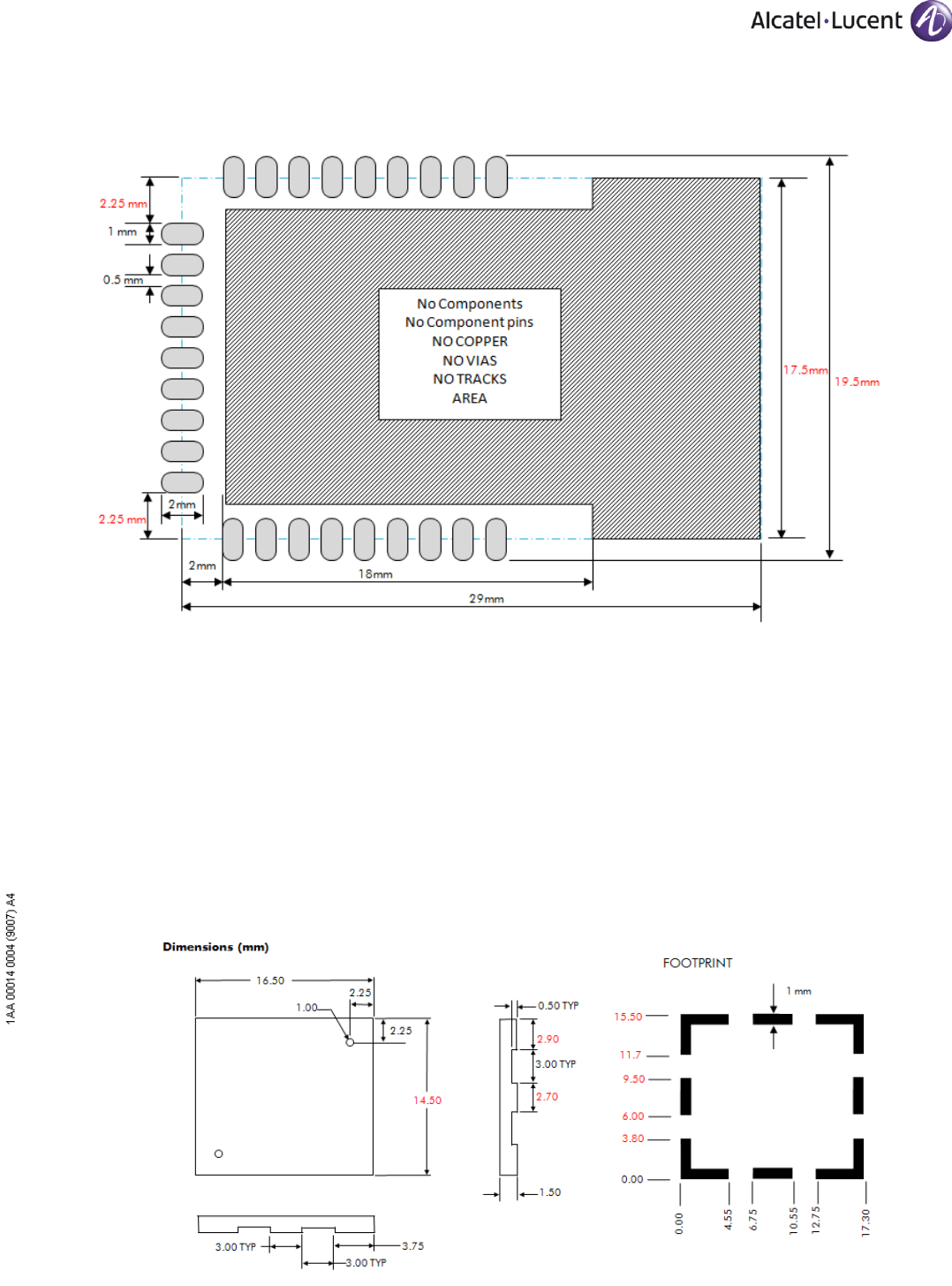
On Main board, the recommended footprint is as follows:
The GND pins must be connected to the GND plane as short as possible, with enough vias. Dotted line is the board
outline.
3.3.4 Shielding Mounting
The target is to deliver a BTDB without shielding. All modules on the market have a shielding. It is required when
the chip and sensitive RF parts are exposed to strong perturbations (WIFI, Cellular,..). It is not yet clear if our
products using the BTHS will be exposed to such conditions. Also for full Bluetooth and RF certification of this
board, the shield may be required.
Therefore we have foreseen provision to equip a one-piece surface mount shield. It is preferred to a two pieces
part for manufacturing reasons. The following reference shall be used:

All rights reserved. Passing on and copying of this document,
use and communication of its contents not permitted
without written authorization from Alcatel.
4. Regulatory Compliance
4.1 FCC statement:
This module has been tested and found to comply with the FCC Part15.
These limits are designed to provide reasonable protection against harmful interference in approved installations.
This equipment generates, uses, and can radiate radio frequency energy and, if not installed and used in
accordance the instructions, may cause harmful interference to radio communications.
However, there is no guarantee that interference will not occur in a particular installation.
This device complies with part 15 of the FCC Rules. Operation is subject to the following two conditions: (1) This
device may not cause harmful interference, and (2) this device must accept any interference received, including
interference that may cause undesired operation.
Modifications or changes to this equipment not expressly approved by Alcatel-Lucent Enterprise may void the
user’s authority to operate this equipment.
The modular transmitter must be equipped with either a permanently affixed label or must be capable of
electronically displaying its FCC identification number
(A) If using a permanently affixed label, the modular transmitter must be labeled with its own FCC identification
number, and, if the FCC identification number is not visible when the module is installed inside another device,
then the outside of the device into which the module is installed must also display a label referring to the enclosed
module. This exterior label can use wording such as the following: “Contains Transmitter Module FCC ID:
OL3BTMOD01” or “Contains FCC ID: OL3BTMOD01.”
(B) If the modular transmitter uses an electronic display of the FCC identification number, the information must be
readily accessible and visible on the modular transmitter or on the device in which it is installed. If the module is
installed inside another device, then the outside of the device into which the module is installed must display a
label referring to the enclosed module. This exterior label can use wording such as the following: “Contains FCC
certified transmitter module(s).”
4.2 IC statement:
The final end product must be labeled in a visible area with the following "Contains transmitter module IC: 1737D-
BTMOD01"
This Class B digital apparatus complies with Canadian ICES-003.
Cetappareilnumérique de la classe B estconforme à la norme NMB-003 du Canada.
This device complies with RSS-210 of the Industry Canada Rules. Operation is subject to the following two
conditions: (1) This device may not cause harmful interference, and (2) this device must accept any interference
received, including interference that may cause undesired operation.
Ce dispositif est conforme à la norme CNR-210 d'Industrie Canada applicable aux appareils radio exempts de
licence. Son fonctionnement est sujet aux deux conditions suivantes: (1) le dispositif ne doit pas produire de
brouillage préjudiciable, et (2) ce dispositif doit accepter tout brouillage reçu, y compris un brouillage susceptible
de provoquer un fonctionnement indésirable.
END OF DOCUMENT