AMPAK Technology AP6234A Wifi Dual Band + BT combo module User Manual
AMPAK Technology Inc. Wifi Dual Band + BT combo module Users Manual
Contents
- 1. User manual
- 2. User Manual.pdf
- 3. User Manual
- 4. Users Manual
Users Manual

Ampak
AP6234AL
Evaluation Kits
User manual
Version 1.2
Revision History
Date
Revision Content
Revised By
Version
2012/12/26
Initial released
Dora
1.0
2013/03/07
Modify figure1
Dora
1.1
2013/06/06
Modify figure1
Dora
1.2
AMPAK Technology Inc. www.ampak.com.tw
Proprietary & Confidential Information
i
Doc. NO:
2006/8/16
v1.0
Federal Communication Commission Interference Statement
This equipment has been tested and found to comply with the limits for a Class B
digital device, pursuant to Part 15 of the FCC Rules. These limits are designed to
provide reasonable protection against harmful interference in a residential installation.
This equipment generates, uses and can radiate radio frequency energy and, if not
installed and used in accordance with the instructions, may cause harmful
interference to radio communications. However, there is no guarantee that
interference will not occur in a particular installation. If this equipment does cause
harmful interference to radio or television reception, which can be determined by
turning the equipment off and on, the user is encouraged to try to correct the
interference by one of the following measures:
- Reorient or relocate the receiving antenna.
- Increase the separation between the equipment and receiver.
- Connect the equipment into an outlet on a circuit different from that
to which the receiver is connected.
- Consult the dealer or an experienced radio/TV technician for help.
FCC Caution: Any changes or modifications not expressly approved by the party
responsible for compliance could void the user's authority to operate this equipment.
This device complies with Part 15 of the FCC Rules. Operation is subject to the
following two conditions: (1) This device may not cause harmful interference, and (2)
this device must accept any interference received, including interference that may
cause undesired operation.
IMPORTANT NOTE:
FCC Radiation Exposure Statement:
This EUT is compliance with SAR for general population/uncontrolled exposure
limits in ANSI/IEEE C95.1-1999 and had been tested in accordance with the
measurement methods and procedures specified in OET Bulletin 65 Supplement C.
Operations in the 5.15-5.25GHz band are restricted to indoor usage only.

2006/8/16
v1.0
This device is intended only for OEM integrators under the following
conditions:
1) The transmitter module may not be co-located with any other transmitter or
antenna,
2) For all products market in US, OEM has to limit the operation channels in CH1
to CH11 for 2.4G band by supplied firmware programming tool. OEM shall not
supply any tool or info to the end-user regarding to Regulatory Domain change.
As long as 2 conditions above are met, further transmitter test will not be required.
However, the OEM integrator is still responsible for testing their end-product for any
additional compliance requirements required with this module installed
IMPORTANT NOTE: In the event that these conditions can not be met (for example
certain laptop configurations or co-location with another transmitter), then the FCC
authorization is no longer considered valid and the FCC ID can not be used on the
final product. In these circumstances, the OEM integrator will be responsible for
re-evaluating the end product (including the transmitter) and obtaining a separate
FCC authorization.
End Product Labeling
The final end product must be labeled in a visible area with the following: “Contains
FCC ID: ZQ6-AP6234A”.
Manual Information To the End User
The OEM integrator has to be aware not to provide information to the end user
regarding how to install or remove this RF module in the user’s manual of the end
product which integrates this module.
The end user manual shall include all required regulatory information/warning as show
in this manual.
2006/8/16
v1.0
Industry Canada statement:
This device complies with Industry Canada licence-exempt RSS standard(s). Operation is
subject to the following two conditions:
(1) this device may not cause interference, and
(2) this device must accept any interference, including interference that may cause
undesired operation of the device.
Le présent appareil est conforme aux CNR d'Industrie Canada applicables aux appareils
radio exempts de licence. L'exploitation est autorisée aux deux conditions suivantes :
(1) l'appareil ne doit pas produire de brouillage, et
(2) l'utilisateur de l'appareil doit accepter tout brouillage radioélectrique subi, même si le
brouillage est susceptible d'en compromettre le fonctionnement.
(i) the device for operation in the band 5150-5250 MHz is only for indoor use to reduce
the potential for harmful interference to co-channel mobile satellite systems;
(ii) the maximum antenna gain permitted for devices in the bands 5250-5350 MHz and
5470-5725 MHz shall comply with the e.i.r.p. limit; and
(iii) the maximum antenna gain permitted for devices in the band 5725-5825 MHz shall
comply with the e.i.r.p. limits specified for point-to-point and non point-to-point operation
as appropriate.
(iv) Users should also be advised that high-power radars are allocated as primary users
(i.e. priority users) of the bands 5250-5350 MHz and 5650-5850 MHz and that these
radars could cause interference and/or damage to LE-LAN devices.
Avertissement:
(i) les dispositifs fonctionnant dans la bande 5150-5250 MHz sont réservés uniquement pour une
utilisation à l’intérieur afin de réduire les risques de brouillage préjudiciable aux systèmes de
satellites mobiles utilisant les mêmes canaux;
(ii) le gain maximal d’antenne permis pour les dispositifs utilisant les bandes 5 250-5 350 MHz et 5
470-5 725 MHz doit se conformer à la limite de p.i.r.e.;
(iii) le gain maximal d’antenne permis (pour les dispositifs utilisant la bande 5 725-5 825 MHz) doit se
conformer à la limite de p.i.r.e. spécifiée pour l’exploitation point à point et non point à point, selon le
cas.
(iv) De plus, les utilisateurs devraient aussi être avisés que les utilisateurs de radars de haute
puissance sont désignés utilisateurs principaux (c.-à-d., qu’ils ont la priorité) pour les bandes 5 250-5
350 MHz et 5 650-5 850 MHz et que ces radars pourraient causer du brouillage et/ou des dommages
aux dispositifs LAN-EL.
2006/8/16
v1.0
Radiation Exposure Statement:
The product comply with the Canada portable RF exposure limit set forth for an uncontrolled
environment and are safe for intended operation as described in this manual. The further RF
exposure reduction can be achieved if the product can be kept as far as possible from the user body
or set the device to lower output power if such function is available.
Déclaration d'exposition aux radiations:
Le produit est conforme aux limites d'exposition pour les appareils portables RF pour les Etats-Unis
et le Canada établies pour un environnement non contrôlé. Le produit est sûr pour un fonctionnement
tel que décrit dans ce manuel. La réduction aux expositions RF peut être augmentée si l'appareil
peut être conservé aussi loin que possible du corps de l'utilisateur ou que le dispositif est réglé sur la
puissance de sortie la plus faible si une telle fonction est disponible.
This device is intended only for OEM integrators under the following conditions:
1) The transmitter module may not be co-located with any other transmitter or antenna.
As long as 1 condition above are met, further transmitter test will not be required. However, the OEM
integrator is still responsible for testing their end-product for any additional compliance requirements
required with this module installed.
Cet appareil est conçu uniquement pour les intégrateurs OEM dans les conditions suivantes:
1) Le module émetteur peut ne pas être coïmplanté avec un autre émetteur ou antenne.
Tant que les 1 condition ci-dessus sont remplies, des essais supplémentaires sur l'émetteur ne
seront pas nécessaires. Toutefois, l'intégrateur OEM est toujours responsable des essais sur son
produit final pour toutes exigences de conformité supplémentaires requis pour ce module installé.
IMPORTANT NOTE:
In the event that these conditions can not be met (for example certain laptop configurations or co-
location with another transmitter), then the Canada authorization is no longer considered valid and
the IC ID can not be used on the final product. In these circumstances, the OEM integrator will be
responsible for re-evaluating the end product (including the transmitter) and obtaining a separate
Canada authorization.
NOTE IMPORTANTE:
Dans le cas où ces conditions ne peuvent être satisfaites (par exemple pour certaines configurations
d'ordinateur portable ou de certaines co-localisation avec un autre émetteur), l'autorisation du
Canada n'est plus considéré comme valide et l'ID IC ne peut pas être utilisé sur le produit final. Dans
ces circonstances, l'intégrateur OEM sera chargé de réévaluer le produit final (y compris l'émetteur)
et l'obtention d'une autorisation distincte au Canada.
End Product Labeling
The final end product must be labeled in a visible area with the following: “Contains IC:11956A-
AP6234A”.

2006/8/16
v1.0
Plaque signalétique du produit final
Le produit final doit être étiqueté dans un endroit visible avec l'inscription suivante: "Contient des IC:
11956A-AP6234A".
Manual Information To the End User
The OEM integrator has to be aware not to provide information to the end user regarding how to
install or remove this RF module in the user’s manual of the end product which integrates this module.
The end user manual shall include all required regulatory information/warning as show in this manual.
Manuel d'information à l'utilisateur final
L'intégrateur OEM doit être conscient de ne pas fournir des informations à l'utilisateur final quant à la
façon d'installer ou de supprimer ce module RF dans le manuel de l'utilisateur du produit final qui
intègre ce module.
Le manuel de l'utilisateur final doit inclure toutes les informations réglementaires requises et
avertissements comme indiqué dans ce manuel.
This radio transmitter (IC: 11956A-AP6234A) has been approved by Industry Canada to
operate with the antenna types listed below with the maximum permissible gain and
required antenna impedance for each antenna type indicated. Antenna types not included
in this list, having a gain greater than the maximum gain indicated for that type, are strictly
prohibited for use with this device.
Le présent émetteur radio (IC: 11956A-AP6234A) a été approuvé par Industrie Canada
pour fonctionner avec les types d'antenne énumérés ci-dessous et ayant un gain
admissible maximal et l'impédance requise pour chaque type d'antenne. Les types
d'antenne non inclus dans cette liste, ou dont le gain est supérieur au gain maximal
indiqué, sont strictement interdits pour l'exploitation de l'émetteur.
Ant. No.
Type
Operating Frequency (MHz) / Gain (dBi)
Connector
2400~2483.5
5150~5250
5250~5350
5470~5725
5725~5850
1
Dipole(Original)
2
3
3
3
3
UFL
2
PIFA(New)
3.53
5.30
4.93
5.31
5.55
UFL
2006/8/16
v1.0
KCC
해당 무선설비는 전파혼신 가능성이 있으므로 인명안전과 관련된 서비스는 할 수 없음
해당 무선 설비는 5150-5250MHz 대역에서 실내 에서안 사용만 수 있웅.
(Translation: the service related to human safety is not allowed because this device
may have the possibility of the radio interference.)
For RF device using 5150-5250MHz, this device shall be used for indoor only.

802.11b/802.11g/BT 警語
第十二條→經型式認證合格之低率射頻電機,非經許,公司,商或使用者均不得擅自變更頻率大率或
變更
原設計之特性及能
第十四條→低率射頻電機之使用不得影響飛航安及擾合法通信經發現有擾現象時,應
立即停用,並改善
至無擾時方得繼續使用
前項合法通信,指依電信法規定作業之無線電通信 低率射頻電機須忍合法通信或工業科學及醫療用電波輻
射性電機設備之擾
802.11a 警語
無線傳輸設備
(UNII)
在
5.25-5.35
秭赫頻帶操作之無線資訊傳輸設備,限於室使用
(4.7.5)
無線資訊傳輸設備忍合法通信之擾且
不得擾合法通信如造成擾,應立即停用,俟無擾之,始得繼續
使用
(4.7.6)
無線資訊傳設備的製造廠商應確
保頻率穩定性,如依製造廠商使用手冊上所述正常操作,發射的信應維持於操作
頻帶中
(4.7.7)
模組請註
1. 本模組於得認證後將依規定於模組本體標示審驗合格標籤
2. 系統廠商應於上標示本產品含射頻模組: CCAFXXLPXXXXTX)字樣
AMPAK Technology Inc.
Doc. NO:
www.ampak.com.tw
Proprietary & Confidential Information
1
1.
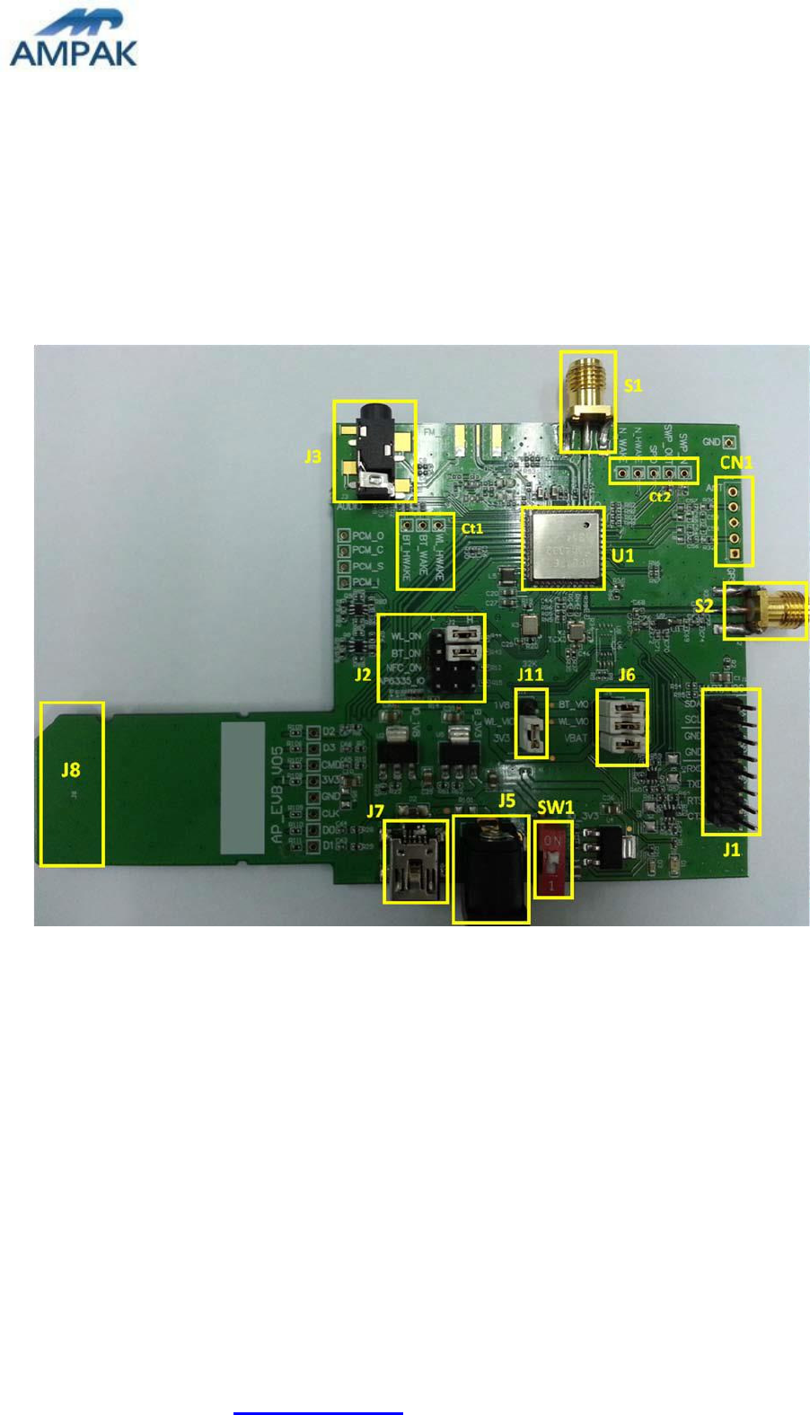
AP6XXX Evaluation Board Introduction
AP6XXX Evaluation board (EVB) likes as figure1. That is designed for IEEE802.11
a/b/g/n/ac WLAN with integrated Bluetooth, FM, NFC and GPS application. It is subject
to provide a convenient environment for customer’s verification on WiFi or Bluetooth
function. There are many controller pins and reserved GPIO on Evaluation board which
describes as below.
Figure1. Top view of AP6XXX EVB
Interface highlights:
1. U1: AP6XXX SIP module.
2. J1: UART interface connects with UART transport board for BT and GPS
measuring, it also provides I2C (SDA/SCL) for NFC measuring.
3. J2: Enable(H) or disable(L) Bluetooth, WiFi, NFC function and AP6335_SDIO I/O
voltage selection.(H for SDIO 3.3V, L for SDIO 1.8V)
4. J3: FM audio out interface.
5. J5: 5V DC adaptor input connector.
6. J6: VBAT / WL_VIO / BT_VIO for main system I/O power path.
7. J7: 5V DC mini USB input connector.
8. J8: Standard SDIO interfaces for Wi-Fi performance measured.
AMPAK Technology Inc.
Doc. NO:
www.ampak.com.tw
Proprietary & Confidential Information
2
9. J11: WL_VIO power path for 1V8 or 3V3 selection.
10. SW1: Power on/off switch.
11. CN1: NFC interface connects with NFC antenna.
12. S1: SMA connector let RF signal in/out path, you could connect with RF cable or
Dipole antenna.
13. S2: SMA connector let GPS RF signal input, you could connect with GPS
antenna.
14. Ct1: WLAN and BT control pins, strongly recommended WL_HWAKE(IRQ)
connected to MCU.
15. Ct2: NFC control pins, strongly recommended N_WAKE and N_H_WAKE
connected to MCU.
2.
WiFi function verification step
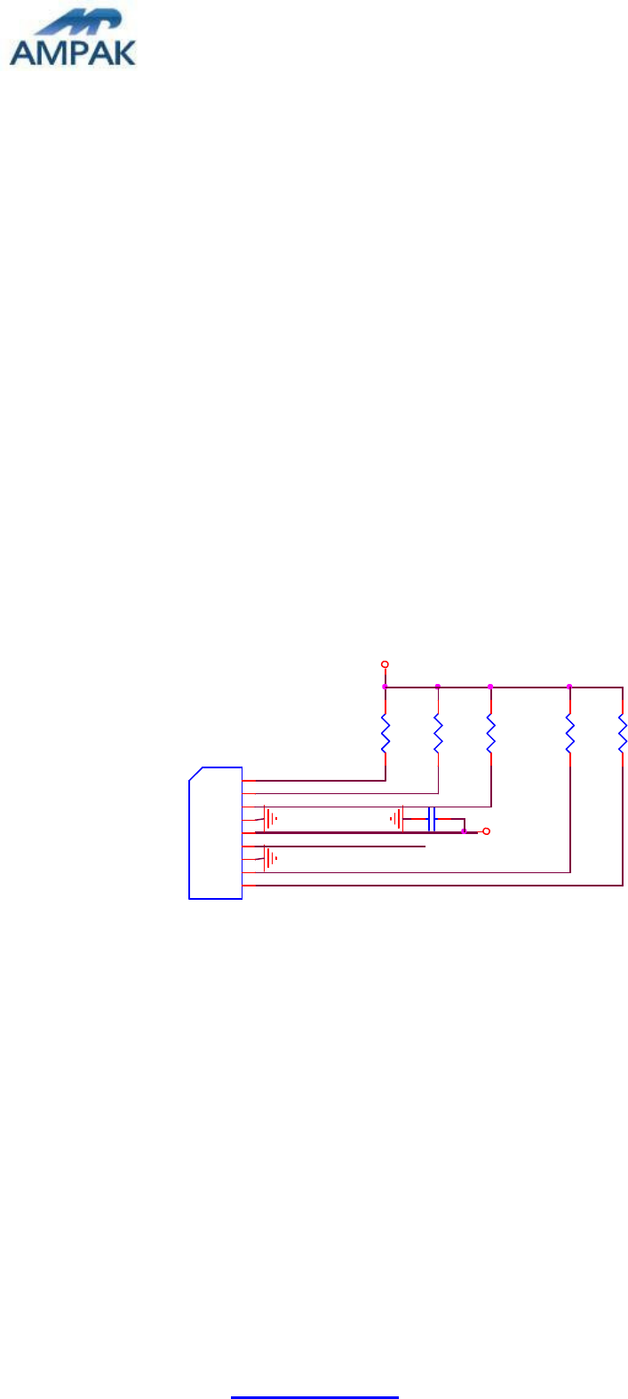
WIFI SDIO: Using external pull up resistors depends on the SDIO supply voltage. For
1.8V, the resistance range is 30KΩ~82KΩ. For 3.3V, its range from 21
KΩ~41 KΩ on the four data lines and the CMD line as the following circuitry.
VIO_3V3
R6 R7 R10
R28 R29
J8 9
SD2 1
SD3 2
SDIO_D2
SDIO_D3
SDIO_CMD
SDCMD 3
GND 4
3.3V 5
SDCLK 6
GND 7
SD0 8
SD1
SDIO_CLK
SDIO_D0
SDIO_D1
1 2
C10
10uF
SDIO_3V3
Golden Finger_9
Figure2. WiFi verification connection interface to Host SDIO
Hardware Setup:
Refer to Figure2 SDIO pin definition connects the J8 interface of AP6XXX
evaluation board to Host SDIO control interface.
Using pull high resistors (R6, R7, R10, R28, R29) that resistance is 30Kohm for
1.8V or 3.3V VDDIO pull up voltage. (Pull high resistors are un-necessary if at
verification phase.)
Connects an external antenna at SMA connector on the evaluation board.
Note to the VDDIO voltage level should be the same with GPIO voltage level of
Host CPU. (VDDIO 3.3V or 1.8V selection by jump J11)
WiFi software setup:
Please follow up software guideline of Ampak official released.
AMPAK Technology Inc.
Doc. NO:
www.ampak.com.tw
Proprietary & Confidential Information
3
3.
Bluetooth function verification step
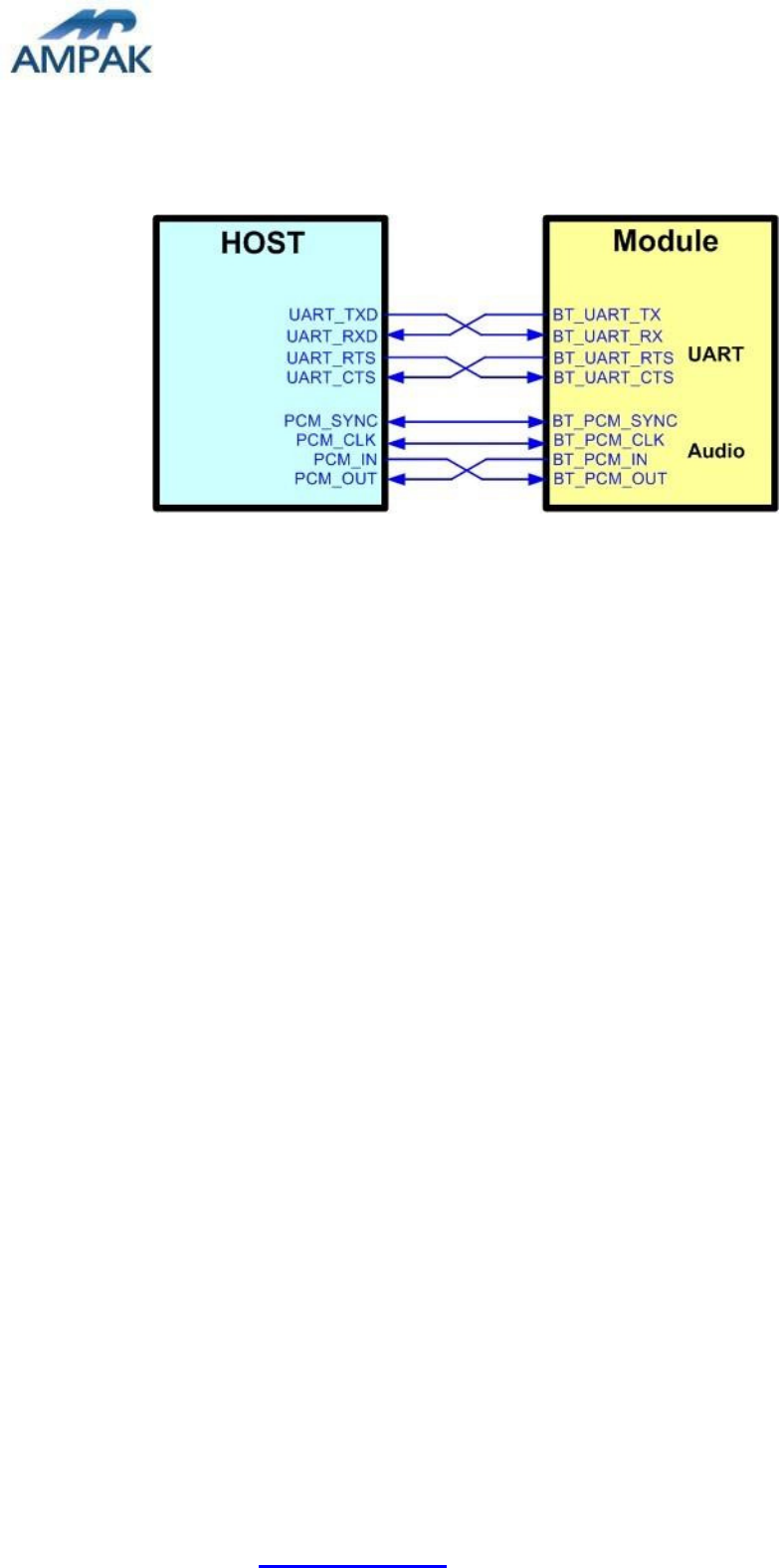
Figure3. Bluetooth verification connection interface to Host UART
Hardware Setup:
Refer to Figure3 UART pin definition connects the J1 interface of AP6XXX
evaluation board to Host UART control interface.
Connects an external antenna at SMA connector on the evaluation board.
Note to the VDDIO voltage level should be the same as GPIO voltage level of
Host CPU.
WiFi and Bluetooth software setup:
Please follow up software guideline of Ampak official released.
AP6234ALNS(HF) Datasheet
AMPAK Technology Inc.
Doc. NO:
www.ampak.com.tw
Proprietary & Confidential Information
4
2.
Features
IEEE 802.11x Key Features
•
Dual-band 2.4GHz/5GHz 802.11a/b/g/n.
•
Single-stream IEEE 802.11n support for 20MHz and 40MHz channels
provides PHY layer rates up to 150Mbps.
•
WLAN host interface options: SDIO v2.0 — up to 50 MHz clock rate
•
Support a single antenna shared between WLAN and Bluetooth.
•
Security: WEP, WPS, WPA, WPA2, WMM, WAPI, AES,…
Bluetooth Features
•
Bluetooth V4.0(BLE) Low Energy with provisions for supporting future
specifications.
•
Bluetooth Class1 or Class2 transmitter operation.
•
BT host digital interface UART(up to 4 Mbps) with support all Bluetooth4.0
package types
•
Multipoint operation with up to seven active ACL links, three active SCO and
eSCO connections.
•
Full support for power savings modes (standard sniff, deep sleep modes)
•
ECI - enhanced coexistence support, ability to coordinate BT SCO
transmissions around WLAN receives
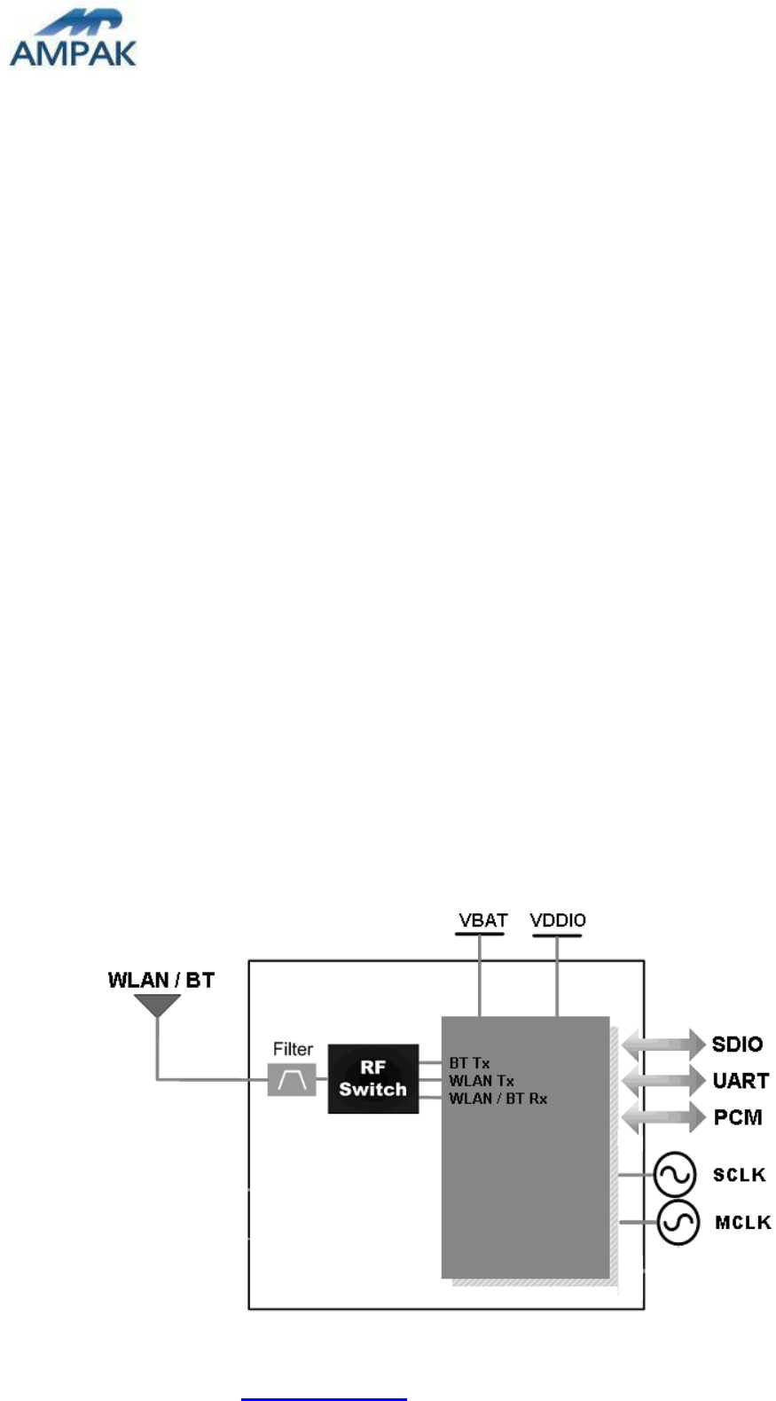
A simplified block diagram of the module is depicted in the figure below.

AP6234ALNS(HF) Datasheet
AMPAK Technology Inc.
Doc. NO:
www.ampak.com.tw
Proprietary & Confidential Information
5
3.
Deliverables
3.1 Deliverables
The following products and software will be part of the product.
Module with packaging
Evaluation Kits
Software utility for integration, performance test.
Product Datasheet.
Agency certified pre-tested report with the adapter board.
3.2 Regulatory certifications
The product delivery is a pre-tested module, without the module level certification. For
module approval, the platform’s antennas are required for the certification.
AP6234ALNS(HF) Datasheet
AMPAK Technology Inc.
Doc. NO:
www.ampak.com.tw
Proprietary & Confidential Information
6
4.
General Specification
4.1 General Specification
Model Name
AP6234
Product Description
Supports Wi-Fi dual mode /Bluetooth functionalities
Dimension
L x W x H: 13.0 x15.0 x 1.3 (typical) mm
WiFi Interface
SDIOV2.0
BT Interface
UART/ PCM
Operating temperature
-30°C to 85°C
Storage temperature
-40°C to 85°C
Humidity
Operating Humidity 10% to 95% Non-Condensing
4.2 Voltages
4.2.1
Absolute Maximum Ratings
Symbol
Description
Min.
Max.
Unit
VBAT
Input supply Voltage
-0.5
5
V
VDDIO
Digital/Bluetooth/SDIO/ I/O Voltage
-0.5
3.6
V
4.2.2
Recommended Operating Rating
The module requires two power supplies: VBAT and VDDIO.
Min.
Typ.
Max.
Unit
Operating Temperature
-30
25
85
deg.C
VBAT
3.0
3.6
4.8
V
VDDIO
1.6
3.3
3.4
V
AP6234ALNS(HF) Datasheet
AMPAK Technology Inc.
Doc. NO:
www.ampak.com.tw
Proprietary & Confidential Information
7
5.
WiFi RF Specification
5.1 2.4GHz & 5GHz RF Specification
Conditions : VBAT=3.6V ; VDDIO=3.3V ; Temp:25°C
Feature
Description
WLAN Standard
IEEE 802.11a/b/g/n, WiFi compliant
Frequency Range
2.400 GHz ~ 2.497 GHz (2.4 GHz ISM Band)
4.900 GHz ~ 5.845 GHz (5.0 GHz ISM Band)
Number of Channels
2.4GHz:Ch1 ~ Ch14
5.0GHz:Please see the table1
Modulation
802.11a : OFDM /64-QAM,16-QAM, QPSK, BPSK
802.11b : DQPSK, DBPSK, CCK
802.11 g/n : OFDM /64-QAM,16-QAM, QPSK, BPSK
Output Power
802.11a /54Mbps : 13 dBm ± 1.5 dB @ EVM -25dB
802.11b /11Mbps : 16 dBm ± 1.5 dB @ EVM -9dB
802.11g /54Mbps : 15 dBm ± 1.5 dB @ EVM -25dB
802.11n /MCS7 : 14 dBm ± 1.5 dB @ EVM -28dB
Receive Sensitivity
(11n,20MHz)
@10% PER
- MCS=0
PER @ -88 dBm, typical
- MCS=1
PER @ -84 dBm, typical
- MCS=2
PER @ -82 dBm, typical
- MCS=3
PER @ -80 dBm, typical
- MCS=4
PER @ -77 dBm, typical
- MCS=5
PER @ -74dBm, typical
- MCS=6
PER @ -72 dBm, typical
- MCS=7
PER @ -70 dBm, typical
Receive Sensitivity
(11n,40MHz)
@10% PER
- MCS=0
PER @ -87 dBm, typical
- MCS=1
PER @ -83 dBm, typical
- MCS=2
PER @ -81 dBm, typical
- MCS=3
PER @ -79 dBm, typical
- MCS=4
PER @ -77 dBm, typical
- MCS=5
PER @ -76 dBm, typical
- MCS=6
PER @ -71 dBm, typical
- MCS=7
PER @ -70 dBm, typical
Receive Sensitivity (11g)
@10% PER
- 6Mbps
PER @ -89 dBm, typical
- 9Mbps
PER @ -88 dBm, typical
- 12Mbps
PER @ -86 dBm, typical
AP6234ALNS(HF) Datasheet
AMPAK Technology Inc.
Doc. NO:
www.ampak.com.tw
Proprietary & Confidential Information
8
- 18Mbps
PER @ -84 dBm, typical
- 24Mbps
PER @ -82 dBm, typical
- 36Mbps
PER @ -78 dBm, typical
- 48Mbps
PER @ -75 dBm, typical
- 54Mbps
PER @ -73 dBm, typical
Receive Sensitivity (11b)
@8% PER
- 1Mbps
PER @ -95 dBm, typical
- 2Mbps
PER @ -94 dBm, typical
- 5.5Mbps
PER @ -90 dBm, typical
- 11Mbps
PER @ -87 dBm, typical
Receive Sensitivity (11a)
@10% PER
- 6Mbps
PER @ -88 dBm, typical
- 9Mbps
PER @ -86 dBm, typical
- 12Mbps
PER @ -84 dBm, typical
- 18Mbps
PER @ -82 dBm, typical
- 24Mbps
PER @ -80 dBm, typical
- 36Mbps
PER @ -78 dBm, typical
- 48Mbps
PER @ -75 dBm, typical
- 54Mbps
PER @ -73 dBm, typical
Maximum Input Level
802.11b : -10 dBm
802.11a/g/n : -20 dBm
Data Rate
802.11a : 6, 9, 12, 18, 24, 36, 48, 54Mbps
802.11b : 1, 2, 5.5, 11Mbps
802.11g : 6, 9, 12, 18, 24, 36, 48, 54Mbps
802.11n: MCS0, MCS1, MCS2, MCS3,
MCS6, MCS7
MCS4,
MCS5,
Antenna Reference
Small antennas with 0~2 dBi peak gain
15GHz Channel table
Band (GHz)
Operating Channel
Numbers
Channel center
frequencies(MHz)
5.15GHz~5.25GHz
36
5180
40
5200
44
5220
48
5240
5.25GHz~5.35GHz
52
5260
56
5280
60
5300
64
5320
5.5GHz~5.7GHz
100
5500
104
5520
108
5540
112
5560
116
5580
120
5600
124
5620
AP6234ALNS(HF) Datasheet
AMPAK Technology Inc.
Doc. NO:
www.ampak.com.tw
Proprietary & Confidential Information
9
128
5640
132
5660
136
5680
140
5700
5.725GHz~5.825GHz
149
5745
153
5765
157
5785
161
5805
6.
Bluetooth Specification
6.1 Bluetooth Specification
Conditions : VBAT=3.6V ; VDDIO=3.3V ; Temp:25°C
Feature
Description
General Specification
Bluetooth Standard
Bluetooth V4.0 of 1, 2 and 3 Mbps.
Host Interface
UART
Antenna Reference
Small antennas with 0~2 dBi peak gain
Frequency Band
2.400 GHz ~ 2483.5 GHz
Number of Channels
79 channels
Modulation
FHSS, GFSK, DPSK, DQPSK
RF Specification
Min.
Typical.
Max.
Output Power (Class 1.5)
10 dBm
Output Power (Class 2)
2 dBm
Sensitivity @ BER=0.1%
for GFSK (1Mbps)
-86 dBm
Sensitivity @ BER=0.01%
for π/4-DQPSK (2Mbps)
-86 dBm
Sensitivity @ BER=0.01%
for 8DPSK (3Mbps)
-80 dBm
Maximum Input Level
GFSK (1Mbps):-20dBm
π/4-DQPSK (2Mbps) :-20dBm
8DPSK (3Mbps) :-20dBm
AP6234ALNS(HF) Datasheet
AMPAK Technology Inc.
Doc. NO:
www.ampak.com.tw
Proprietary & Confidential Information
10
7.
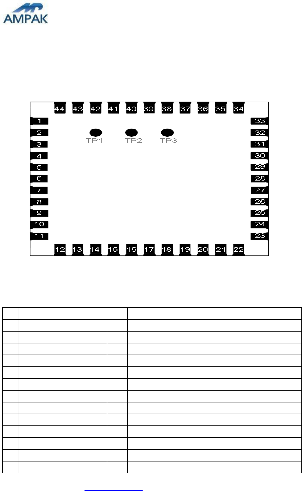
Pin Assignments
7.1 Pin Outline
< TOP VIEW >
7.2 Pin Definition
NO
Name
Type
Description
1
GND
-
Ground connections
2
WL_BT_ANT
I/O
RF I/O port
3
GND
-
Ground connections
4
NC
-
Floating (Don’t connected to ground)
5
NC
-
Floating (Don’t connected to ground)
6
BT_WAKE
I
HOST wake-up Bluetooth device
7
BT_HOST_WAKE
O
Bluetooth device to wake-up HOST
8
NC
-
Floating (Don’t connected to ground)
9
VBAT
P
Main power voltage source input
10
XTAL_IN
I
Floating (Don’t connected to ground)
11
XTAL_OUT
O
Floating (Don’t connected to ground)
12
WL_REG_ON
I
Internal regulators power enable/disable
13
WL_HOST_WAKE
O
WLAN to wake-up HOST
AP6234ALNS(HF) Datasheet
AMPAK Technology Inc.
Doc. NO:
www.ampak.com.tw
Proprietary & Confidential Information
11
14
SDIO_DATA_2
I/O
SDIO data line 2
15
SDIO_DATA_3
I/O
SDIO data line 3
16
SDIO_DATA_CMD
I/O
SDIO command line
17
SDIO_DATA_CLK
I/O
SDIO clock line
18
SDIO_DATA_0
I/O
SDIO data line 0
19
SDIO_DATA_1
I/O
SDIO data line 1
20
GND
-
Ground connections
21
VIN_LDO_OUT
P
Internal Buck voltage generation pin
22
VDDIO
P
I/O Voltage supply input
23
VIN_LDO
P
Internal Buck voltage generation pin
24
LPO
I
Low power oscillator clock input (32.768KHz)
25
PCM_OUT
O
PCM Data output
26
PCM_CLK
I/O
PCM clock
27
PCM_IN
I
PCM data input
28
PCM_SYNC
I/O
PCM sync signal
29
NC
-
Floating (Don’t connected to ground)
30
NC
-
Floating (Don’t connected to ground)
31
GND
-
Ground connections
32
NC
-
Floating (Don’t connected to ground)
33
GND
-
Ground connections
34
BT_RST_N
I
Low asserting reset for Bluetooth core
35
NC
-
Floating (Don’t connected to ground)
36
GND
-
Ground connections
37
NC
-
Floating (Don’t connected to ground)
38
NC
-
Floating (Don’t connected to ground)
39
NC
-
Floating (Don’t connected to ground)
40
NC
-
Floating (Don’t connected to ground)
41
UART_RTS_N
O
Bluetooth UART interface
42
UART_TXD
O
Bluetooth UART interface
43
UART_RXD
I
Bluetooth UART interface
44
UART_CTS_N
I
Bluetooth UART interface
45
TP1
-
Floating (Don’t connected to ground)
46
TP2
-
Floating (Don’t connected to ground)
47
TP3
-
Floating (Don’t connected to ground)