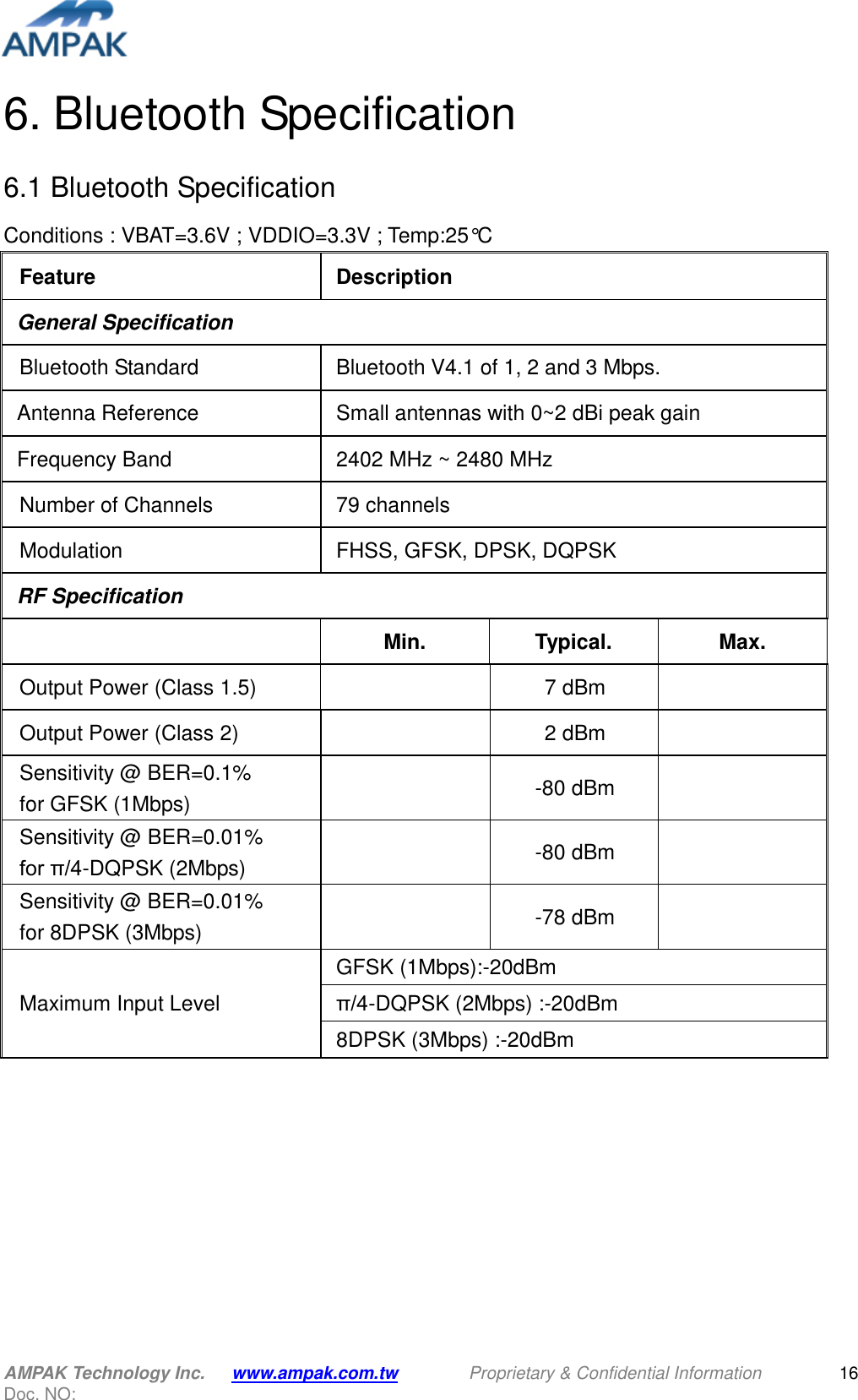
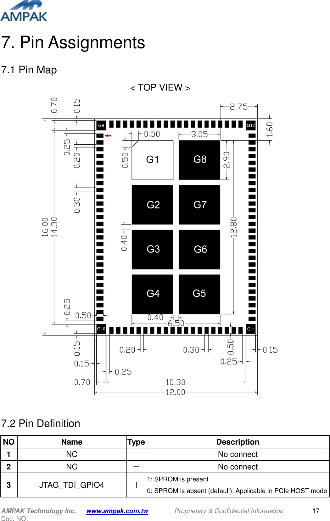
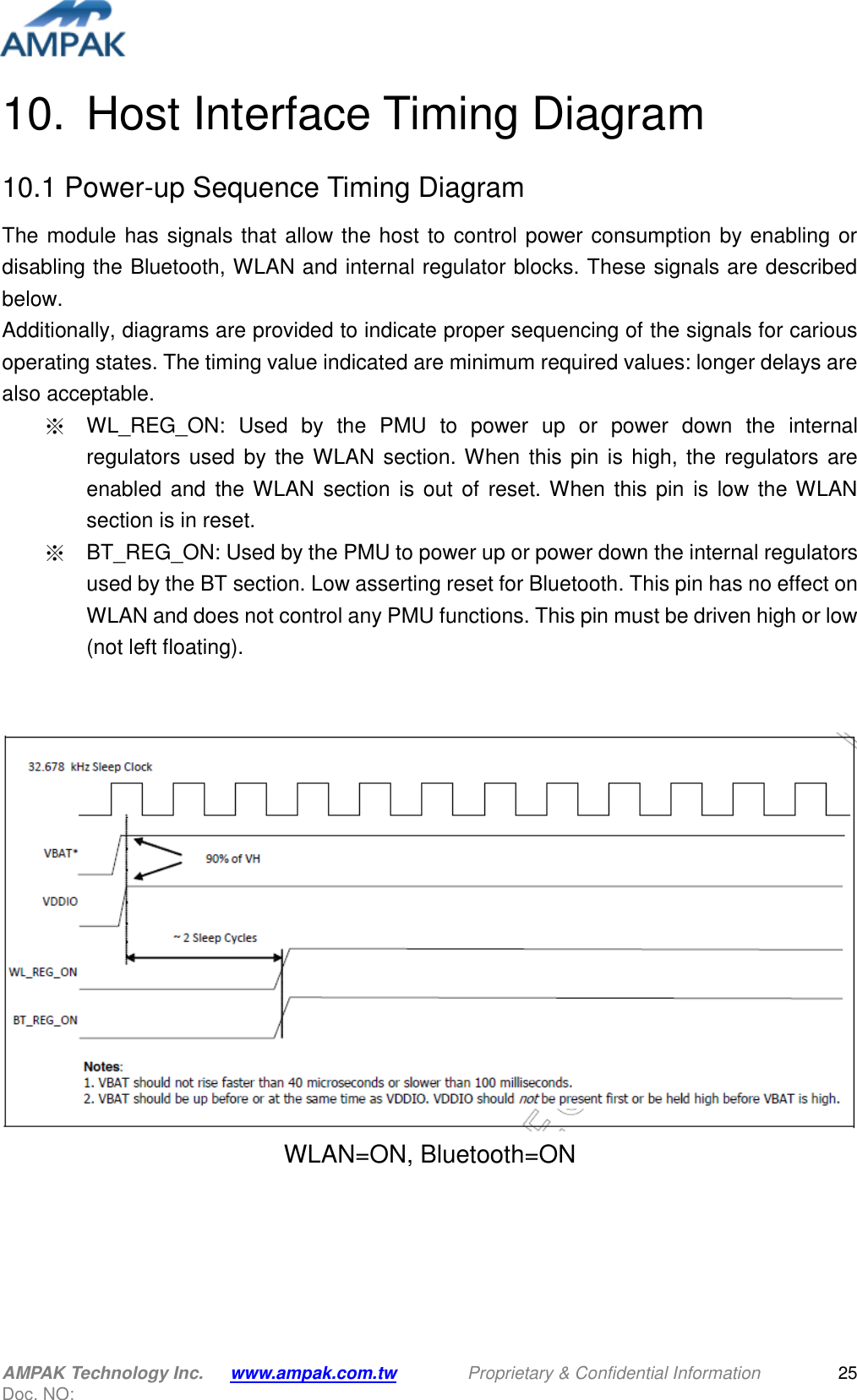
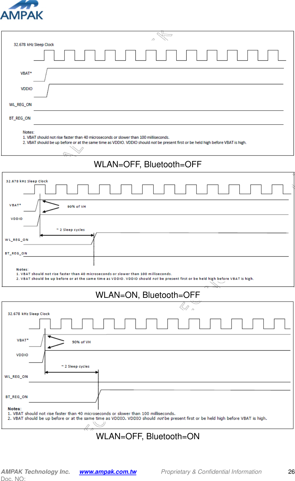
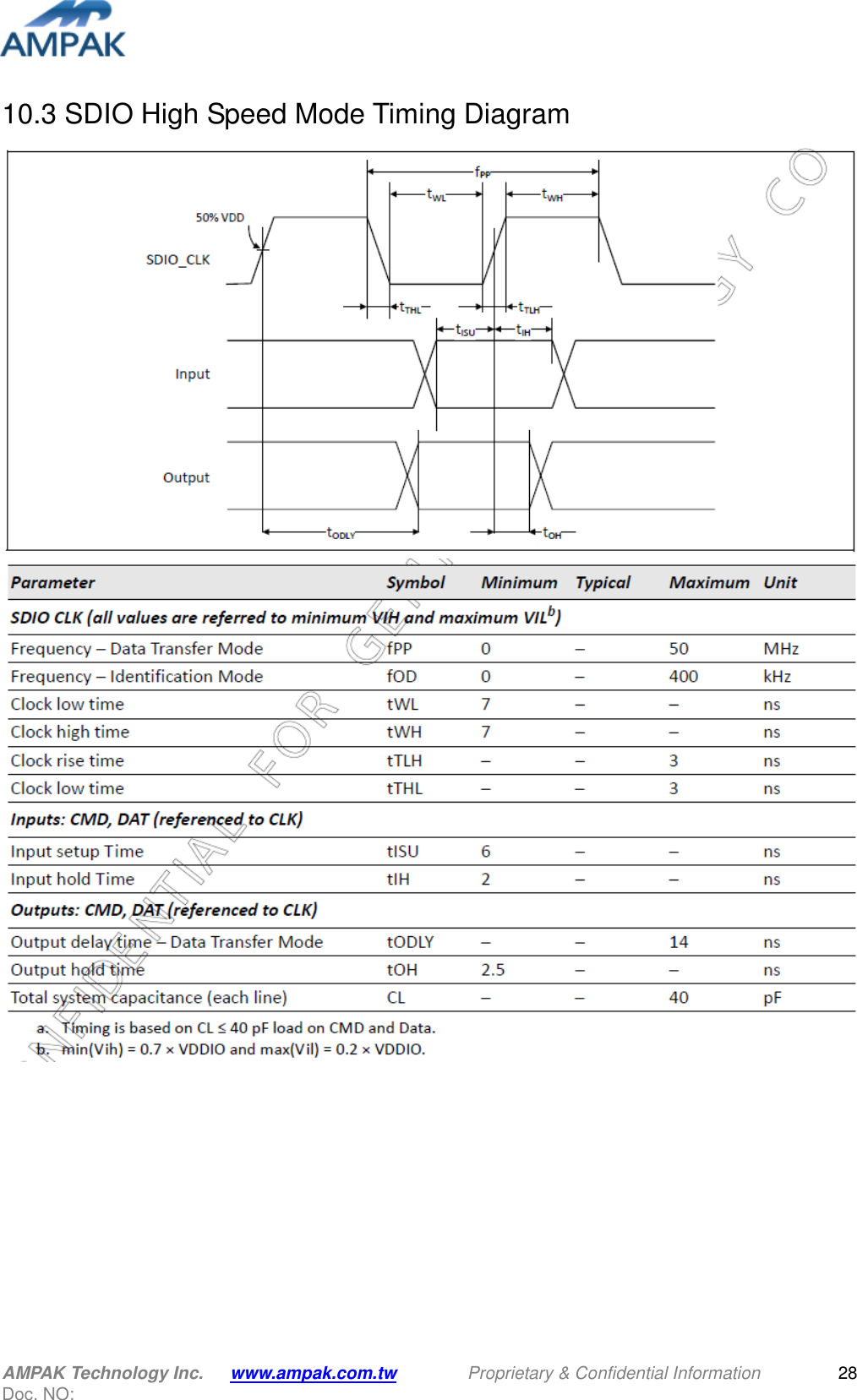
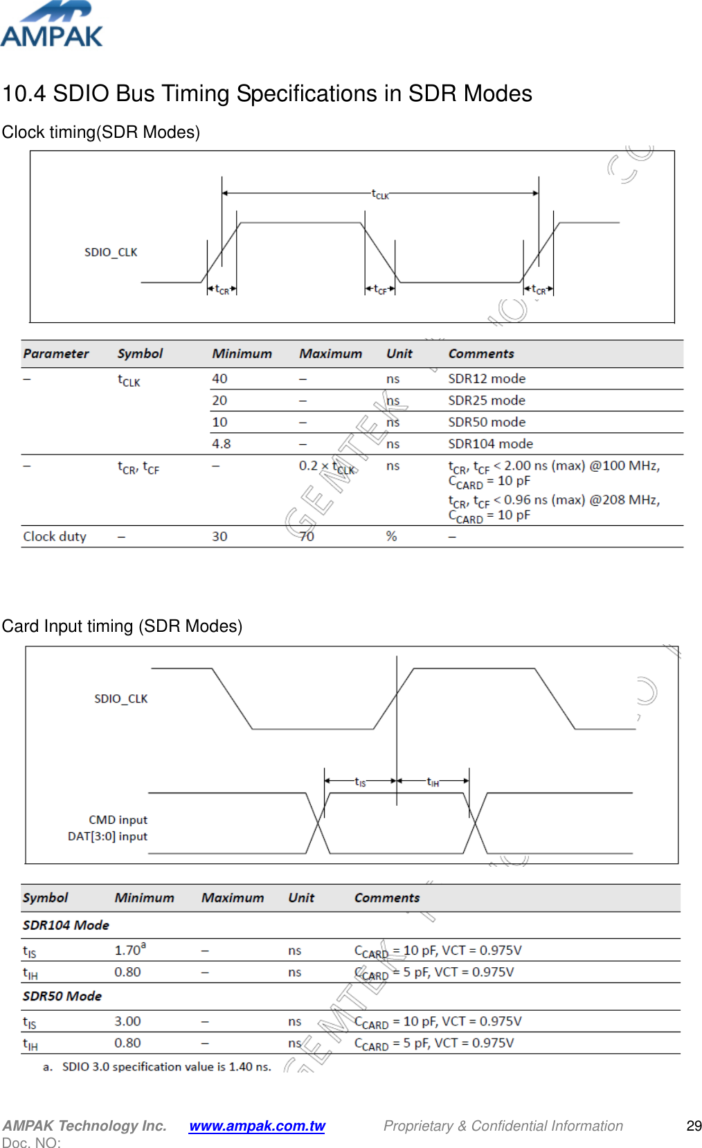
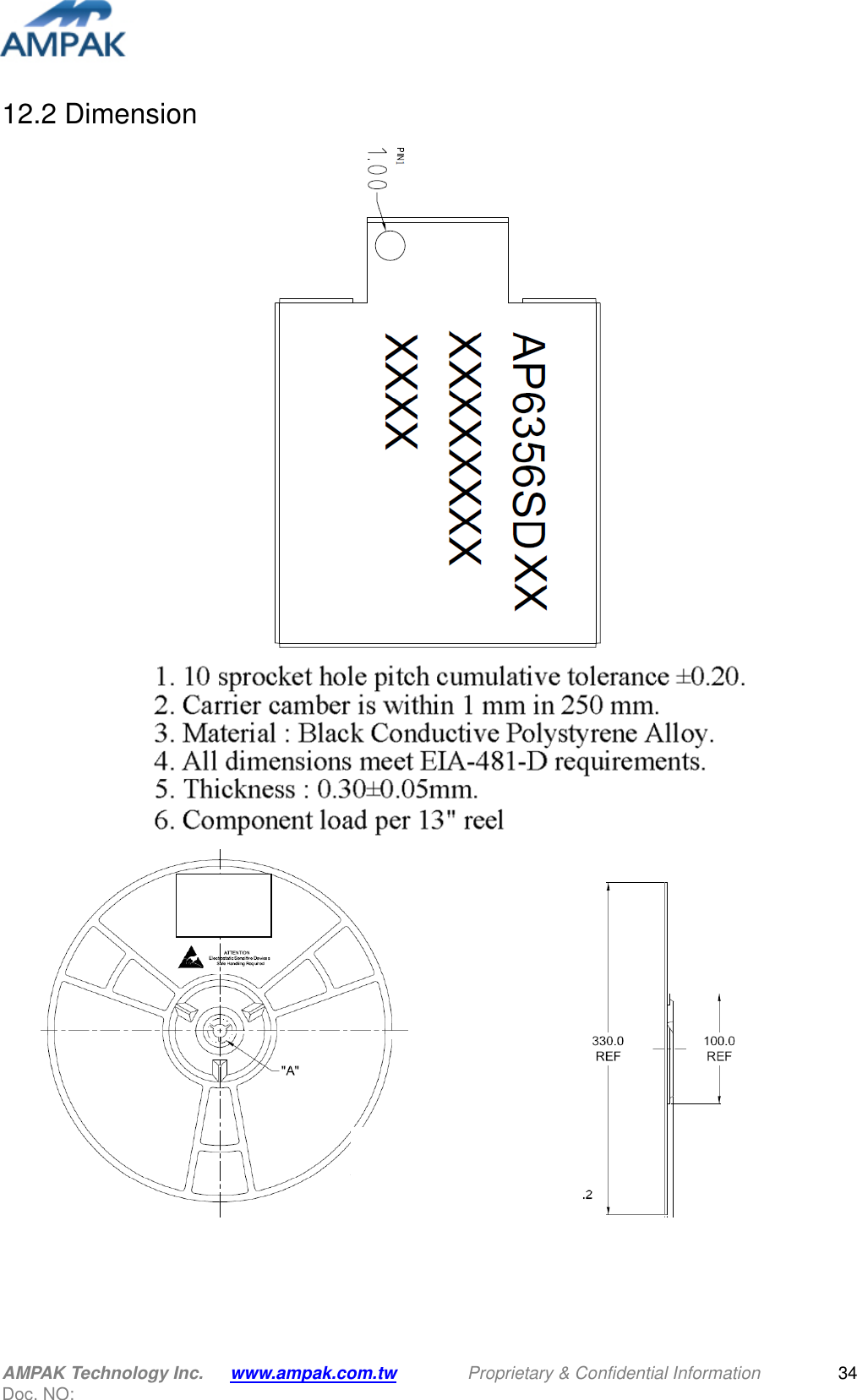
AMPAK Technology AP6356SDXX WLAN module for 802.11abgn(2x2) + 11ac+BT4.1 User Manual User Manuel
AMPAK Technology Inc. WLAN module for 802.11abgn(2x2) + 11ac+BT4.1 User Manuel
UserManual.wiki
>
AMPAK Technology
>
AP6356SDXX User Manual
>
User Manuel
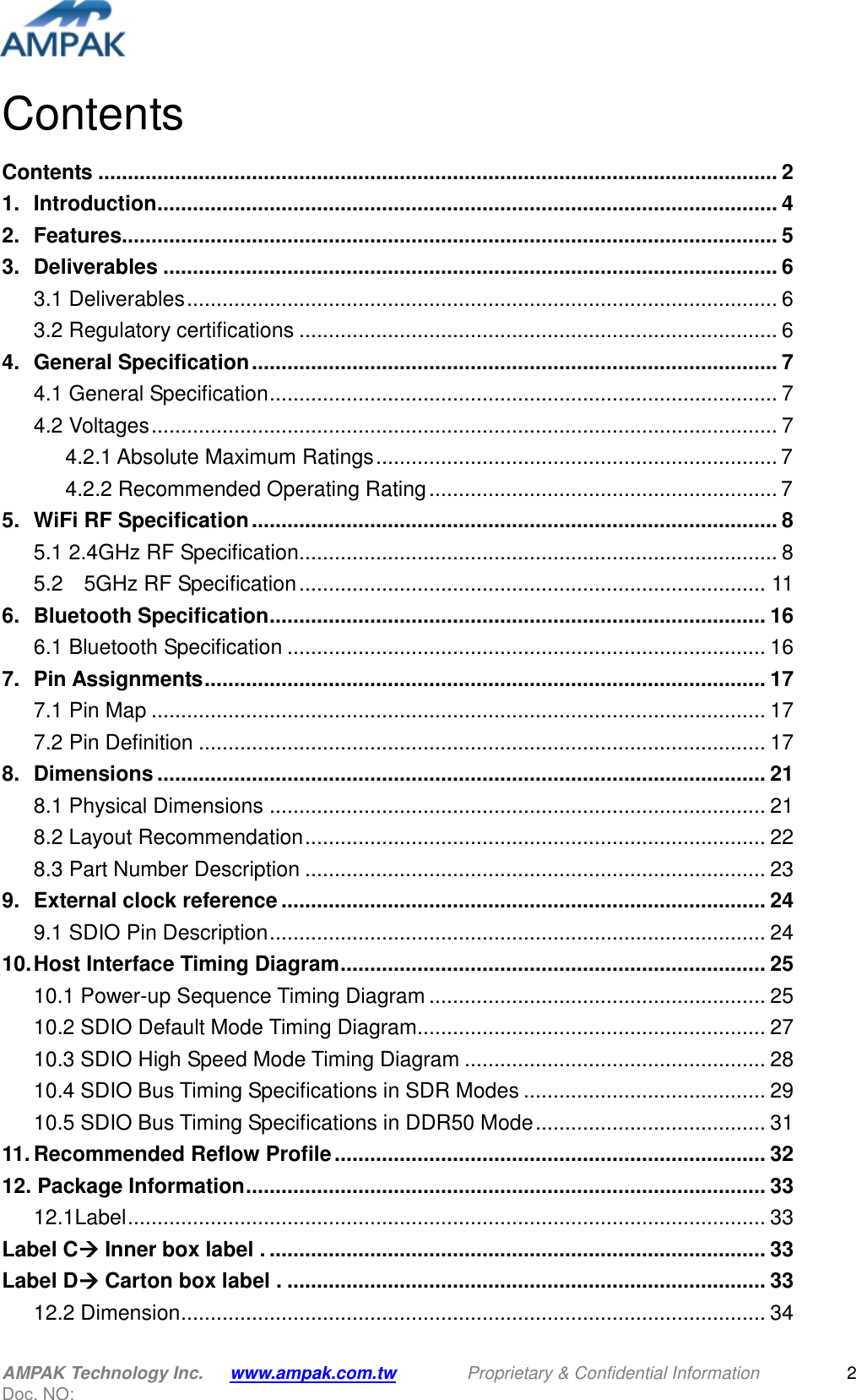
Contents
1.
User Manual
2.
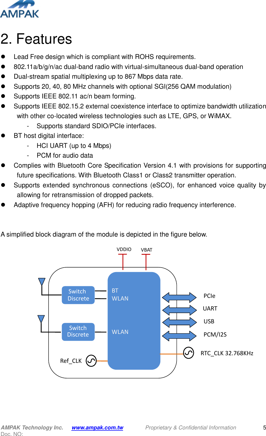
User Manuel
User Manuel
Navigation menu
Upload a User Manual
Namespaces
Wiki Guide
HTML
PDF
Info
Views
User Manual
Discussion / Help
Navigation