AMPAK Technology AP6356SDXX WLAN module for 802.11abgn(2x2) + 11ac+BT4.1 User Manual User Manuel
AMPAK Technology Inc. WLAN module for 802.11abgn(2x2) + 11ac+BT4.1 User Manuel
Contents
- 1. User Manual
- 2. User Manuel
User Manuel

AMPAK Technology Inc. www.ampak.com.tw Proprietary & Confidential Information i
Doc. NO:
AMPAK
AP6356SDXX
Evaluation Kits
User manual
Version 1.0
Revision History
Date
Revision Content
Revised By
Version
2015/12/28
Initial released
Aron
1.0
Federal Communication Commission Interference Statement
This device complies with Part 15 of the FCC Rules. Operation is subject to
the following two conditions: (1) This device may not cause harmful
interference, and (2) this device must accept any interference received,
including interference that may cause undesired operation.
This equipment has been tested and found to comply with the limits for a
Class B digital device, pursuant to Part 15 of the FCC Rules. These limits
are designed to provide reasonable protection against harmful interference in a
residential installation. This equipment generates, uses and can radiate radio
frequency energy and, if not installed and used in accordance with the
instructions, may cause harmful interference to radio communications.
However, there is no guarantee that interference will not occur in a particular
installation. If this equipment does cause harmful interference to radio or
television reception, which can be determined by turning the equipment off
and on, the user is encouraged to try to correct the interference by one of the
following measures:
- Reorient or relocate the receiving antenna.
- Increase the separation between the equipment and receiver.
- Connect the equipment into an outlet on a circuit different from that
to which the receiver is connected.
- Consult the dealer or an experienced radio/TV technician for help.
FCC Caution: Any changes or modifications not expressly approved by the
party responsible for compliance could void the user's authority to operate this
equipment.
This transmitter must not be co-located or operating in conjunction with any
other antenna or transmitter.

Radiation Exposure Statement:
The product comply with the FCC portable RF exposure limit set forth for an
uncontrolled environment and are safe for intended operation as described in
this manual. The further RF exposure reduction can be achieved if the product
can be kept as far as possible from the user body or set the device to lower
output power if such function is available.
This device is intended only for OEM integrators under the following conditions:
1) The transmitter module may not be co-located with any other transmitter
or antenna.
As long as 2 conditions above are met, further transmitter test will not be
required. However, the OEM integrator is still responsible for testing their
end-product for any additional compliance requirements required with this
module installed
IMPORTANT NOTE: In the event that these conditions can not be met (for
example certain laptop configurations or co-location with another transmitter),
then the FCC authorization is no longer considered valid and the FCC ID can
not be used on the final product. In these circumstances, the OEM integrator
will be responsible for re-evaluating the end product (including the transmitter)
and obtaining a separate FCC authorization.
End Product Labeling
The product can be kept as far as possible from the user body or set the device
to lower output power if such function is available. The final end product must
be labeled in a visible area with the following: “Contains FCC
ID:ZQ6-AP6356SDXX”. The grantee's FCC ID can be used only when all
FCC compliance requirements are met.
Manual Information To the End User
The OEM integrator has to be aware not to provide information to the end user
regarding how to install or remove this RF module in the user’s manual of the
end product which integrates this module.
The end user manual shall include all required regulatory information/warning
as show in this manual.

Industry Canada statement:
This device complies with ISED’s licence-exempt RSSs. Operation is subject to the
following two conditions: (1) This device may not cause harmful interference, and (2)
this device must accept any interference received, including interference that may
cause undesired operation.
Le présent appareil est conforme aux CNR d’ ISED applicables aux appareils radio
exempts de licence. L’exploitation est autorisée aux deux conditions suivantes : (1) le
dispositif ne doit pas produire de brouillage préjudiciable, et (2) ce dispositif doit
accepter tout brouillage reçu, y compris un brouillage susceptible de provoquer un
fonctionnement indésirable.
Radiation Exposure Statement:
The product comply with the Canada portable RF exposure limit set forth for an
uncontrolled environment and are safe for intended operation as described in this
manual. The further RF exposure reduction can be achieved if the product can be kept
as far as possible from the user body or set the device to lower output power if such
function is available.
Déclaration d'exposition aux radiations:
Le produit est conforme aux limites d'exposition pour les appareils portables RF pour
les Etats-Unis et le Canada établies pour un environnement non contrôlé.
Le produit est sûr pour un fonctionnement tel que décrit dans ce manuel. La réduction
aux expositions RF peut être augmentée si l'appareil peut être conservé aussi loin que
possible du corps de l'utilisateur ou que le dispositif est réglé sur la puissance de sortie
la plus faible si une telle fonction est disponible.
This device is intended only for OEM integrators under the following conditions: (For
module device use)
1) The transmitter module may not be co-located with any other transmitter or
antenna.
As long as 2 conditions above are met, further transmitter test will not be required.
However, the OEM integrator is still responsible for testing their end-product for any
additional compliance requirements required with this module installed.
Cet appareil est conçu uniquement pour les intégrateurs OEM dans les conditions
suivantes: (Pour utilisation de dispositif module)

1) Le module émetteur peut ne pas être coïmplanté avec un autre émetteur ou antenne.
Tant que les 2 conditions ci-dessus sont remplies, des essais supplémentaires sur
l'émetteur ne seront pas nécessaires. Toutefois, l'intégrateur OEM est toujours
responsable des essais sur son produit final pour toutes exigences de conformité
supplémentaires requis pour ce module installé.
IMPORTANT NOTE:
In the event that these conditions can not be met (for example certain laptop
configurations or co-location with another transmitter), then the Canada authorization
is no longer considered valid and the IC ID can not be used on the final product. In
these circumstances, the OEM integrator will be responsible for re-evaluating the end
product (including the transmitter) and obtaining a separate Canada authorization.
NOTE IMPORTANTE:
Dans le cas où ces conditions ne peuvent être satisfaites (par exemple pour certaines
configurations d'ordinateur portable ou de certaines co-localisation avec un autre
émetteur), l'autorisation du Canada n'est plus considéré comme valide et l'ID IC ne
peut pas être utilisé sur le produit final. Dans ces circonstances, l'intégrateur OEM
sera chargé de réévaluer le produit final (y compris l'émetteur) et l'obtention d'une
autorisation distincte au Canada.
End Product Labeling
The product can be kept as far as possible from the user body or set the device to
lower output power if such function is available. The final end product must be
labeled in a visible area with the following: “Contains IC: ”.
Plaque signalétique du produit final
L'appareil peut être conservé aussi loin que possible du corps de l'utilisateur ou que le
dispositif est réglé sur la puissance de sortie la plus faible si une telle fonction est
disponible. Le produit final doit être étiqueté dans un endroit visible avec l'inscription
suivante: "Contient des IC: ".
Manual Information To the End User
The OEM integrator has to be aware not to provide information to the end user
regarding how to install or remove this RF module in the user’s manual of the end
product which integrates this module.

The end user manual shall include all required regulatory information/warning as
show in this manual.
Manuel d'information à l'utilisateur final
L'intégrateur OEM doit être conscient de ne pas fournir des informations à l'utilisateur
final quant à la façon d'installer ou de supprimer ce module RF dans le manuel de
l'utilisateur du produit final qui intègre ce module.
Le manuel de l'utilisateur final doit inclure toutes les informations réglementaires
requises et avertissements comme indiqué dans ce manuel.
Caution :
(i) the device for operation in the band 5150-5250 MHz is only for indoor use to
reduce the potential for harmful interference to co-channel mobile satellite systems;
(ii) the maximum antenna gain permitted for devices in the bands 5250-5350 MHz
and 5470-5725 MHz shall be such that the equipment still complies with the e.i.r.p.
limit;
(iii) the maximum antenna gain permitted for devices in the band 5725-5850 MHz
shall be such that the equipment still complies with the e.i.r.p. limits specified for
point-to-point and non-point-to-point operation as appropriate; and
(iv) the worst-case tilt angle(s) necessary to remain compliant with the e.i.r.p. elevation
mask requirement set forth in Section 6.2.2(3) shall be clearly indicated.
(v) Users should also be advised that high-power radars are allocated as primary users
(i.e. priority users) of the bands 5250-5350 MHz and 5650-5850 MHz and that these
radars could cause interference and/or damage to LE-LAN devices.
Avertissement:
Le guide d’utilisation des dispositifs pour réseaux locaux doit inclure des instructions
précises sur les restrictions susmentionnées, notamment :
(i) les dispositifs fonctionnant dans la bande 5150-5250 MHz sont réservés
uniquement pour une utilisation à l’intérieur afin de réduire les risques de brouillage
préjudiciable aux systèmes de satellites mobiles utilisant les mêmes canaux;
(ii) le gain maximal d'antenne permis pour les dispositifs utilisant les bandes de 5250 à 5

350 MHz et de 5470 à 5725 MHz doit être conforme à la limite de la p.i.r.e;
(iii) le gain maximal d'antenne permis (pour les dispositifs utilisant la bande de 5 725 à 5
850 MHz) doit être conforme à la limite de la p.i.r.e. spécifiée pour l'exploitation point à
point et l’exploitation non point à point, selon le cas;
(iv) les pires angles d’inclinaison nécessaires pour rester conforme à l’exigence de la
p.i.r.e. applicable au masque d’élévation, et énoncée à la section 6.2.2 3), doivent être
clairement indiqués.
(v) De plus, les utilisateurs devraient aussi être avisés que les utilisateurs de radars de
haute puissance sont désignés utilisateurs principaux (c.-à-d., qu’ils ont la priorité)
pour les bandes 5250-5350 MHz et 5650-5850 MHz et que ces radars pourraient
causer du brouillage et/ou des dommages aux dispositifs LAN-EL.

第十二條 經型式認證合格之低功率射頻電機,非經許可,公司、商號或使用者均
不得擅自變更頻率、加大功率或變更原設計之特性及功能。
第十四條 低功率射頻電機之使用不得影響飛航安全及干擾合法通信;經發現有干
擾現象時,應立即停用,並改善至無干擾時方得繼續使用。
前項合法通信,指依電信法規定作業之無線電通信。
低功率射頻電機須忍受合法通信或工業、科學及醫療用電波輻射性電機設
備之干擾。
1. 本模組於取得認證後將依規定於模組本體標示審驗合格標籤。
2. 系統廠商應於平台上標示「本產品內含射頻模組:XXXyyyLPDzzzz-x」字 樣 。
AMPAK Technology Inc. www.ampak.com.tw Proprietary & Confidential Information
Doc. NO:
3
1. AP6356SDXX Evaluation Board Introduction
AP6356SDXX Evaluation board (EVB) likes as figure1. That is designed for IEEE802.11
a/b/g/n/ac 2x2 WLAN with integrated Bluetooth. It is subject to provide a convenient
environment for customer’s verification on WiFi or Bluetooth function. There are many
controller pins and reserved GPIO on Evaluation board which describes as below.
Figure1. Top view of AP6356SDXX EVB
Interface highlights:
1. U1: AP6356SDXX SIP module.
2. J1: UART interface connects with UART transport board for BT.
3. J80: PCIE interface connects with PCIE transport board for WIFI.
4. J3: Enable(H) or disable(L) Bluetooth and WiFi function.
5. J4: PCIE interface strapping option
6. J5: 5V DC adaptor input connector.
7. J6: 3V3 RF/ VBAT / WL_VIO / BT_VIO for main system I/O power path.
8. J7/J9: 5V DC mini USB input connector.
9. J10: GPIO_2 (input/output) and GPIO_3 (input/output)
10. J11: WL_VIO power path for 1V8 or 3V3 selection.
11. A1: I-PEX connector let RF signal in/out path, you could connect with RF cable or
J10
J4
J3
J1
A2
U1
A1
J80
ct2
ct3
ct4
J7
J5
J9
J11
J6
ct1
AMPAK Technology Inc. www.ampak.com.tw Proprietary & Confidential Information
Doc. NO:
4
Dipole antenna.
12. A2: I-PEX connector let RF signal in/out path, you could connect with RF cable or
Dipole antenna.
13. Ct1-Ct4: WLAN and BT control pins, strongly recommended WL_H_WAKE(IRQ)
connected to MCU.
2. WiFi function verification step
WIFI PCIe: PCIe interface definition as below J80 dip connector and this should be used
3.3V for PCIe voltage.
Figure3. WiFi verification connection interface to Host PCIE
Hardware Setup:
Refer to Figure3 PCIE pin definition connects the J80 interface of
AP6356SDXX evaluation board to Host PCIE control interface.
Connects an external antenna at I-PEX connector on the evaluation board.
Note to the VDDIO voltage level should be the same with GPIO voltage level of
Host CPU. (VDDIO 3.3V or 1.8V selection by jump J11)
Pull High J4 are necessary .
WiFi software setup:
Please follow up software guideline of Ampak official released.
AMPAK Technology Inc. www.ampak.com.tw Proprietary & Confidential Information
Doc. NO:
5
3. Bluetooth function verification step
UART:
Figure4. Bluetooth verification connection interface to Host UART
Hardware Setup:
Refer to Figure4 UART pin definition connects the J1 interface of AP6356SDXX
evaluation board to Host UART control interface.
Connects an external antenna at I-PEX connector on the evaluation board.
Note to the VDDIO voltage level should be the same as GPIO voltage level of
Host CPU.
USB:
Figure5. Bluetooth verification connection interface to Host USB

AMPAK Technology Inc. www.ampak.com.tw Proprietary & Confidential Information
Doc. NO:
6
Hardware Setup:
Refer to Figure5 USB pin definition connects the J9 interface of AP6356SDXX
evaluation board to Host USB control interface.
Connects an external antenna at I-PEX connector on the evaluation board.
WiFi and Bluetooth software setup:
Please follow up software guideline of Ampak official released.
AMPAK Technology Inc. www.ampak.com.tw Proprietary & Confidential Information
Doc. NO:
正基科技股份有限公司
SPECIFICATION
SPEC. NO.: REV: 1.6
DATE: 09. 07.2015
PRODUCT NAME: AP6356SDXX
Customer APPROVED
Company
Representative
Signature
PREPARED
REVIEW
APPROVED
DCC ISSUE
PM
QA

AMPAK Technology Inc. www.ampak.com.tw Proprietary & Confidential Information
Doc. NO:
AMPAK
AP6356SDXX
2x2 WiFi + Bluetooth4.1
Module Spec Sheet

AMPAK Technology Inc. www.ampak.com.tw Proprietary & Confidential Information
Doc. NO:
1
Revision History
Date
Revision Content
Revised By
Version
2014/09/25
-Preliminary
Brian
1.0
2014/10/26
-Pin definition modified
Brian
1.1
2014/12/11
-Pin definition modified
Brian
1.2
2015/03/18
-Layout and Bluetooth Spec modified
- Pin map and physical dimension modified
Dora
1.3
2015/05/12
-Add Part Number Description
Dora
1.4
2015/06/29
-Add Packet type and total pins
Dora
1.5
2015/09/07
-Modify label quantity and MSL
Dora
1.6

AMPAK Technology Inc. www.ampak.com.tw Proprietary & Confidential Information
Doc. NO:
2
Contents
Contents ................................................................................................................... 2
1. Introduction ......................................................................................................... 4
2. Features............................................................................................................... 5
3. Deliverables ........................................................................................................ 6
3.1 Deliverables .................................................................................................... 6
3.2 Regulatory certifications ................................................................................. 6
4. General Specification ......................................................................................... 7
4.1 General Specification ...................................................................................... 7
4.2 Voltages .......................................................................................................... 7
4.2.1 Absolute Maximum Ratings .................................................................... 7
4.2.2 Recommended Operating Rating ........................................................... 7
5. WiFi RF Specification ......................................................................................... 8
5.1 2.4GHz RF Specification................................................................................. 8
5.2 5GHz RF Specification ............................................................................... 11
6. Bluetooth Specification .................................................................................... 16
6.1 Bluetooth Specification ................................................................................. 16
7. Pin Assignments ............................................................................................... 17
7.1 Pin Map ........................................................................................................ 17
7.2 Pin Definition ................................................................................................ 17
8. Dimensions ....................................................................................................... 21
8.1 Physical Dimensions .................................................................................... 21
8.2 Layout Recommendation .............................................................................. 22
8.3 Part Number Description .............................................................................. 23
9. External clock reference .................................................................................. 24
9.1 SDIO Pin Description .................................................................................... 24
10. Host Interface Timing Diagram ........................................................................ 25
10.1 Power-up Sequence Timing Diagram ......................................................... 25
10.2 SDIO Default Mode Timing Diagram........................................................... 27
10.3 SDIO High Speed Mode Timing Diagram ................................................... 28
10.4 SDIO Bus Timing Specifications in SDR Modes ......................................... 29
10.5 SDIO Bus Timing Specifications in DDR50 Mode ....................................... 31
11. Recommended Reflow Profile ......................................................................... 32
12. Package Information ........................................................................................ 33
12.1Label ............................................................................................................ 33
Label C Inner box label . .................................................................................... 33
Label D Carton box label . ................................................................................. 33
12.2 Dimension ................................................................................................... 34


AMPAK Technology Inc. www.ampak.com.tw Proprietary & Confidential Information
Doc. NO:
4
1. Introduction
AMPAK Technology would like to announce a low-cost and low-power consumption module
which has all of the WiFi and Bluetooth functionalities. The highly integrated module makes
the possibilities of web browsing, VoIP, Bluetooth headsets applications. With seamless
roaming capabilities and advanced security, also could interact with different vendors’
802.11a/b/g/n/ac 2x2 Access Points in the wireless LAN.
The wireless module complies with IEEE 802.11 a/b/g/n/ac 2x2 MIMO standard and it can
achieve up to a speed of 867Mbps with dual stream in 802.11n to connect the wireless LAN.
The integrated module provides SDIO/PCIe interface for WiFi, UART / USB/ PCM interface
for Bluetooth.
This compact module is a total solution for a combination of WiFi + BT technologies. The
module is specifically developed for Smart phones and Portable devices.
AMPAK Technology Inc. www.ampak.com.tw Proprietary & Confidential Information
Doc. NO:
5
2. Features
Lead Free design which is compliant with ROHS requirements.
802.11a/b/g/n/ac dual-band radio with virtual-simultaneous dual-band operation
Dual-stream spatial multiplexing up to 867 Mbps data rate.
Supports 20, 40, 80 MHz channels with optional SGI(256 QAM modulation)
Supports IEEE 802.11 ac/n beam forming.
Supports IEEE 802.15.2 external coexistence interface to optimize bandwidth utilization
with other co-located wireless technologies such as LTE, GPS, or WiMAX.
- Supports standard SDIO/PCIe interfaces.
BT host digital interface:
- HCI UART (up to 4 Mbps)
- PCM for audio data
Complies with Bluetooth Core Specification Version 4.1 with provisions for supporting
future specifications. With Bluetooth Class1 or Class2 transmitter operation.
Supports extended synchronous connections (eSCO), for enhanced voice quality by
allowing for retransmission of dropped packets.
Adaptive frequency hopping (AFH) for reducing radio frequency interference.
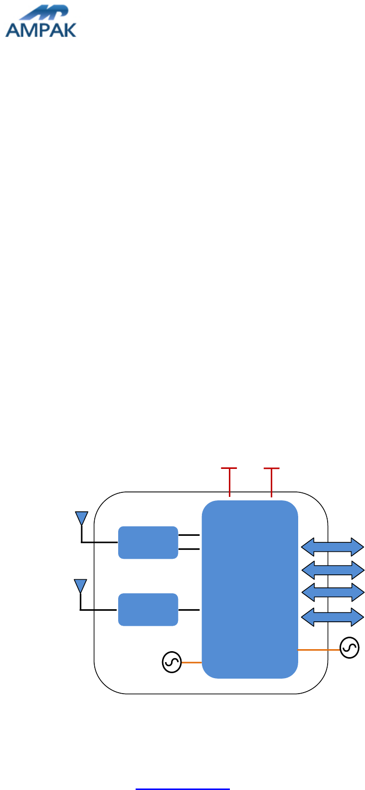
A simplified block diagram of the module is depicted in the figure below.
Switch
UART
PCM/I2S
RTC_CLK 32.768KHz
Ref_CLK
Discrete
BT
WLAN
WLAN
Switch
Discrete
VBAT
VDDIO
USB
PCIe

AMPAK Technology Inc. www.ampak.com.tw Proprietary & Confidential Information
Doc. NO:
6
3. Deliverables
3.1 Deliverables
The following products and software will be part of the product.
Module with packaging
Evaluation Kits
Software utility for integration, performance test.
Product Datasheet.
Agency certified pre-tested report with the adapter board.
3.2 Regulatory certifications
The product delivery is a pre-tested module, without the module level certification. For
module approval, the platform’s antennas are required for the certification.
AMPAK Technology Inc. www.ampak.com.tw Proprietary & Confidential Information
Doc. NO:
7
4. General Specification
4.1 General Specification
4.2 Voltages
4.2.1 Absolute Maximum Ratings
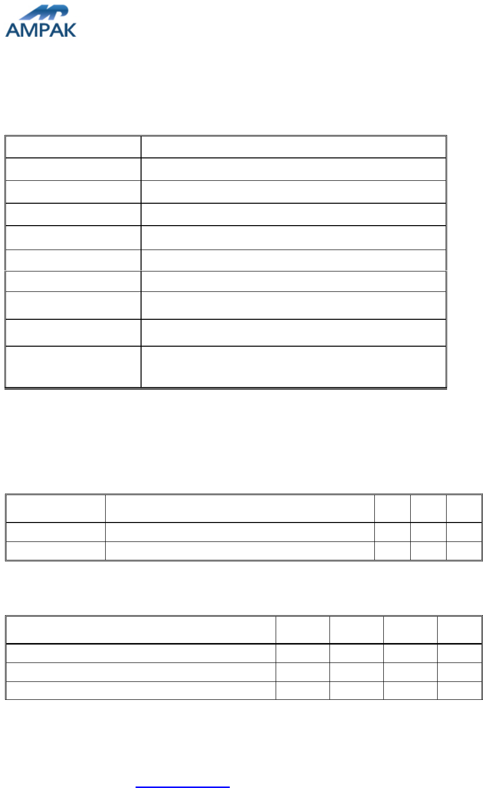
Symbol
Description
Min.
Max.
Unit
VBAT
Input supply Voltage
-0.5
5.5
V
VDDIO
Digital/Bluetooth/SDIO/ I/O Voltage
-0.5
3.8
V
4.2.2 Recommended Operating Rating
The module requires two power supplies: VBAT and VDDIO.
Min.
Typ.
Max.
Unit
Operating Temperature
-10
25
65
deg.C
VBAT
3.0
3.6
4.8
V
VDDIO
1.7
-
3.6
V
Model Name
AP6356SDXX
Product Description
Support WiFi/Bluetooth functionalities
Dimension
L x W x H: 16 x 12 x 1.6 (typical) mm
WiFi Interface
Support PCIe
BT Interface
UART / USB / PCM
Package
M.2 1216 Solder down
Total Pin
108 Pins
Operating temperature
-10°C to 65°C
Storage temperature
-40°C to 85°C
Humidity
Operating Humidity 10% to 95% Non-Condensing
Storage Humidity 5% to 95% Non-Condensing
AMPAK Technology Inc. www.ampak.com.tw Proprietary & Confidential Information
Doc. NO:
8
5. WiFi RF Specification
5.1 2.4GHz RF Specification
Conditions : VBAT=3.6V ; VDDIO=3.3V ; Temp:25°C
Feature
Description
WLAN Standard
IEEE 802.11a/b/g/n/ac WiFi compliant
Frequency Range
2.400 GHz ~ 2.497 GHz (2.4 GHz ISM Band)
Number of Channels
2.4GHz:Ch1 ~ Ch14
Modulation
802.11b : DQPSK, DBPSK, CCK
802.11 g/n : OFDM /64-QAM,16-QAM, QPSK, BPSK
Output Power
802.11b /11Mbps : 16 dBm ± 1.5 dB @ EVM -9dB
802.11g /54Mbps : 15 dBm ± 1.5 dB @ EVM -25dB
802.11n /MCS7 : 14 dBm ± 1.5 dB @ EVM -28dB
SISO Receive
Sensitivity (11b,20MHz)
@8% PER
- 1Mbps PER @ -93 dBm, typical
- 2Mbps PER @ -91 dBm, typical
- 5.5Mbps PER @ -88 dBm, typical
- 11Mbps PER @ -86 dBm, typical
SISO Receive
Sensitivity (11g,20MHz)
@10% PER
- 6Mbps PER @ -90 dBm, typical
- 9Mbps PER @ -89 dBm, typical
- 12Mbps PER @ -88 dBm, typical
- 18Mbps PER @ -85 dBm, typical
- 24Mbps PER @ -82 dBm, typical
- 36Mbps PER @ -79 dBm, typical
- 48Mbps PER @ -74 dBm, typical
- 54Mbps PER @ -72 dBm, typical
MIMO Receive
Sensitivity (11g,20MHz)
@10% PER
- 6Mbps PER @ -91 dBm, typical
- 9Mbps PER @ -91 dBm, typical
- 12Mbps PER @ -90 dBm, typical
- 18Mbps PER @ -88 dBm, typical
- 24Mbps PER @ -85 dBm, typical
- 36Mbps PER @ -82 dBm, typical
- 48Mbps PER @ -77 dBm, typical
- 54Mbps PER @ -75 dBm, typical
SISO Receive
Sensitivity (11n,20MHz)
@10% PER
- MCS=0 PER @ -90 dBm, typical
- MCS=1 PER @ -87 dBm, typical
- MCS=2 PER @ -85 dBm, typical
AMPAK Technology Inc. www.ampak.com.tw Proprietary & Confidential Information
Doc. NO:
9
- MCS=3 PER @ -81 dBm, typical
- MCS=4 PER @ -78 dBm, typical
- MCS=5 PER @ -73 dBm, typical
- MCS=6 PER @ -72 dBm, typical
- MCS=7 PER @ -70 dBm, typical
MIMO Receive
Sensitivity (11n,20MHz)
@10% PER
- MCS=0 PER @ -91 dBm, typical
- MCS=1 PER @ -90 dBm, typical
- MCS=2 PER @ -88 dBm, typical
- MCS=3 PER @ -85 dBm, typical
- MCS=4 PER @ -81 dBm, typical
- MCS=5 PER @ -76 dBm, typical
- MCS=6 PER @ -74 dBm, typical
- MCS=7 PER @ -71 dBm, typical
- MCS=8 PER @ -88 dBm, typical
- MCS=15 PER @ -69 dBm, typical
SISO Receive
Sensitivity (11n,40MHz)
@10% PER
- MCS=0 PER @ -87 dBm, typical
- MCS=1 PER @ -83 dBm, typical
- MCS=2 PER @ -82 dBm, typical
- MCS=3 PER @ -79 dBm, typical
- MCS=4 PER @ -75 dBm, typical
- MCS=5 PER @ -71 dBm, typical
- MCS=6 PER @ -69 dBm, typical
- MCS=7 PER @ -68 dBm, typical
MIMO Receive
Sensitivity (11n,40MHz)
@10% PER
- MCS=0 PER @ -89 dBm, typical
- MCS=1 PER @ -87 dBm, typical
- MCS=2 PER @ -85 dBm, typical
- MCS=3 PER @ -82 dBm, typical
- MCS=4 PER @ -78 dBm, typical
- MCS=5 PER @ -74 dBm, typical
- MCS=6 PER @ -72 dBm, typical
- MCS=7 PER @ -71 dBm, typical
- MCS=8 PER @ -87 dBm, typical
- MCS=15 PER @ -68 dBm, typical
SISO Receive
Sensitivity
(11ac,20MHz) @10%
PER
- MCS=0, NSS1 PER @ -89 dBm, typical
- MCS=1, NSS1 PER @ -86 dBm, typical
- MCS=2, NSS1 PER @ -85 dBm, typical
- MCS=3, NSS1 PER @ -81 dBm, typical
AMPAK Technology Inc. www.ampak.com.tw Proprietary & Confidential Information
Doc. NO:
10
- MCS=4, NSS1 PER @ -78 dBm, typical
- MCS=5, NSS1 PER @ -73 dBm, typical
- MCS=6, NSS1 PER @ -71 dBm, typical
- MCS=7, NSS1 PER @ -70 dBm, typical
- MCS=8, NSS1 PER @ -67 dBm, typical
MIMO Receive
Sensitivity
(11ac,20MHz) @10%
PER
- MCS=0, NSS1 PER @ -89 dBm, typical
- MCS=1, NSS1 PER @ -88 dBm, typical
- MCS=2, NSS1 PER @ -87 dBm, typical
- MCS=3, NSS1 PER @ -84 dBm, typical
- MCS=4, NSS1 PER @ -81 dBm, typical
- MCS=5, NSS1 PER @ -76 dBm, typical
- MCS=6, NSS1 PER @ -75 dBm, typical
- MCS=7, NSS1 PER @ -73 dBm, typical
- MCS=8, NSS1 PER @ -69 dBm, typical
- MCS=0, NSS2 PER @ -89 dBm, typical
- MCS=8, NSS2 PER @ -65 dBm, typical
SISO Receive
Sensitivity
(11ac,40MHz) @10%
PER
- MCS=0, NSS1 PER @ -86 dBm, typical
- MCS=1, NSS1 PER @ -84 dBm, typical
- MCS=2, NSS1 PER @ -82 dBm, typical
- MCS=3, NSS1 PER @ -79 dBm, typical
- MCS=4, NSS1 PER @ -75 dBm, typical
- MCS=5, NSS1 PER @ -71 dBm, typical
- MCS=6, NSS1 PER @ -69 dBm, typical
- MCS=7, NSS1 PER @ -68 dBm, typical
- MCS=8, NSS1 PER @ -63 dBm, typical
- MCS=9, NSS1 PER @ -62 dBm, typical
MIMO Receive
Sensitivity
(11ac,40MHz) @10%
PER
- MCS=0, NSS1 PER @ -88 dBm, typical
- MCS=1, NSS1 PER @ -87 dBm, typical
- MCS=2, NSS1 PER @ -85 dBm, typical
- MCS=3, NSS1 PER @ -82 dBm, typical
- MCS=4, NSS1 PER @ -77 dBm, typical
- MCS=5, NSS1 PER @ -74 dBm, typical
- MCS=6, NSS1 PER @ -72 dBm, typical
- MCS=7, NSS1 PER @ -71 dBm, typical
- MCS=8, NSS1 PER @ -67 dBm, typical
- MCS=9, NSS1 PER @ -65 dBm, typical
- MCS=0, NSS2 PER @ -86 dBm, typical
AMPAK Technology Inc. www.ampak.com.tw Proprietary & Confidential Information
Doc. NO:
11
- MCS=9, NSS2 PER @ -61 dBm, typical
Maximum Input Level
802.11b : -10 dBm
802.11g/n : -20 dBm
Antenna Reference
Small antennas with 0~2 dBi peak gain
5.2 5GHz RF Specification
Conditions : VBAT=3.6V ; VDDIO=3.3V ; Temp:25°C
Feature
Description
WLAN Standard
IEEE 802.11a/n 2x2, WiFi compliant
Frequency Range
4.900 GHz ~ 5.845 GHz (5.0 GHz ISM Band)
Number of Channels
5.0GHz:Please see the table1
Modulation
802.11a : OFDM /64-QAM,16-QAM, QPSK, BPSK
802.11n : OFDM /64-QAM,16-QAM, QPSK, BPSK
802.11ac : OFDM /256-QAM
Output Power
802.11a /54Mbps : 13 dBm ± 1.5 dB @ EVM -25dB
802.11n /MCS7 : 12 dBm ± 1.5 dB @ EVM -28dB
802.11ac /MCS9 : 10 dBm ± 1.5 dB @ EVM -32dB
SISO Receive Sensitivity
(11a,20MHz) @10% PER
- 6Mbps PER @ -90 dBm, typical
- 9Mbps PER @ -88 dBm, typical
- 12Mbps PER @ -87 dBm, typical
- 18Mbps PER @ -84 dBm, typical
- 24Mbps PER @ -81 dBm, typical
- 36Mbps PER @ -78 dBm, typical
- 48Mbps PER @ -73 dBm, typical
- 54Mbps PER @ -71 dBm, typical
MIMO Receive Sensitivity
(11a,20MHz) @10% PER
- 6Mbps PER @ -90 dBm, typical
- 9Mbps PER @ -90 dBm, typical
- 12Mbps PER @ -89 dBm, typical
- 18Mbps PER @ -87 dBm, typical
- 24Mbps PER @ -84 dBm, typical
- 36Mbps PER @ -81 dBm, typical
- 48Mbps PER @ -76 dBm, typical
- 54Mbps PER @ -72 dBm, typical
SISO Receive Sensitivity
(11n,20MHz) @10% PER
- MCS=0 PER @ -89 dBm, typical
- MCS=1 PER @ -86 dBm, typical
AMPAK Technology Inc. www.ampak.com.tw Proprietary & Confidential Information
Doc. NO:
12
- MCS=2 PER @ -84 dBm, typical
- MCS=3 PER @ -81 dBm, typical
- MCS=4 PER @ -77 dBm, typical
- MCS=5 PER @ -72 dBm, typical
- MCS=6 PER @ -71 dBm, typical
- MCS=7 PER @ -69 dBm, typical
MIMO Receive Sensitivity
(11n,20MHz) @10% PER
- MCS=0 PER @ -90 dBm, typical
- MCS=1 PER @ -89 dBm, typical
- MCS=2 PER @ -87 dBm, typical
- MCS=3 PER @ -84 dBm, typical
- MCS=4 PER @ -80 dBm, typical
- MCS=5 PER @ -75 dBm, typical
- MCS=6 PER @ -74 dBm, typical
- MCS=7 PER @ -72 dBm, typical
- MCS=8 PER @ -89 dBm, typical
- MCS=15 PER @ -69 dBm, typical
SISO Receive Sensitivity
(11n,40MHz) @10% PER
- MCS=0 PER @ -86 dBm, typical
- MCS=1 PER @ -83 dBm, typical
- MCS=2 PER @ -81 dBm, typical
- MCS=3 PER @ -78 dBm, typical
- MCS=4 PER @ -74 dBm, typical
- MCS=5 PER @ -70 dBm, typical
- MCS=6 PER @ -68 dBm, typical
- MCS=7 PER @ -67 dBm, typical
MIMO Receive Sensitivity
(11n,40MHz) @10% PER
- MCS=0 PER @ -88 dBm, typical
- MCS=1 PER @ -86 dBm, typical
- MCS=2 PER @ -84 dBm, typical
- MCS=3 PER @ -81 dBm, typical
- MCS=4 PER @ -77 dBm, typical
- MCS=5 PER @ -73 dBm, typical
- MCS=6 PER @ -71 dBm, typical
- MCS=7 PER @ -70 dBm, typical
- MCS=8 PER @ -86 dBm, typical
- MCS=15 PER @ -67 dBm, typical
SISO Receive Sensitivity
(11ac,20MHz) @10% PER
- MCS=0, NSS1 PER @ -87 dBm, typical
- MCS=1, NSS1 PER @ -85 dBm, typical
- MCS=2, NSS1 PER @ -83 dBm, typical
AMPAK Technology Inc. www.ampak.com.tw Proprietary & Confidential Information
Doc. NO:
13
- MCS=3, NSS1 PER @ -80 dBm, typical
- MCS=4, NSS1 PER @ -76 dBm, typical
- MCS=5, NSS1 PER @ -71 dBm, typical
- MCS=6, NSS1 PER @ -70 dBm, typical
- MCS=7, NSS1 PER @ -69 dBm, typical
- MCS=8, NSS1 PER @ -65 dBm, typical
MIMO Receive Sensitivity
(11ac,20MHz) @10% PER
- MCS=0, NSS1 PER @ -89 dBm, typical
- MCS=1, NSS1 PER @ -88 dBm, typical
- MCS=2, NSS1 PER @ -86 dBm, typical
- MCS=3, NSS1 PER @ -83 dBm, typical
- MCS=4, NSS1 PER @ -79 dBm, typical
- MCS=5, NSS1 PER @ -74 dBm, typical
- MCS=6, NSS1 PER @ -73 dBm, typical
- MCS=7, NSS1 PER @ -72 dBm, typical
- MCS=8, NSS1 PER @ -68 dBm, typical
- MCS=0, NSS2 PER @ -88 dBm, typical
- MCS=8, NSS2 PER @ -64 dBm, typical
SISO Receive Sensitivity
(11ac,40MHz) @10% PER
- MCS=0, NSS1 PER @ -85 dBm, typical
- MCS=1, NSS1 PER @ -82 dBm, typical
- MCS=2, NSS1 PER @ -80 dBm, typical
- MCS=3, NSS1 PER @ -77 dBm, typical
- MCS=4, NSS1 PER @ -74 dBm, typical
- MCS=5, NSS1 PER @ -69 dBm, typical
- MCS=6, NSS1 PER @ -68 dBm, typical
- MCS=7, NSS1 PER @ -67 dBm, typical
- MCS=8, NSS1 PER @ -62 dBm, typical
- MCS=9, NSS1 PER @ -61 dBm, typical
MIMO Receive Sensitivity
(11ac,40MHz) @10% PER
- MCS=0, NSS1 PER @ -87 dBm, typical
- MCS=1, NSS1 PER @ -85 dBm, typical
- MCS=2, NSS1 PER @ -83 dBm, typical
- MCS=3, NSS1 PER @ -80 dBm, typical
- MCS=4, NSS1 PER @ -77 dBm, typical
- MCS=5, NSS1 PER @ -72 dBm, typical
- MCS=6, NSS1 PER @ -71 dBm, typical
- MCS=7, NSS1 PER @ -70 dBm, typical
- MCS=8, NSS1 PER @ -65 dBm, typical
- MCS=9, NSS1 PER @ -64 dBm, typical
AMPAK Technology Inc. www.ampak.com.tw Proprietary & Confidential Information
Doc. NO:
14
- MCS=0, NSS2 PER @ -85 dBm, typical
- MCS=9, NSS2 PER @ -60 dBm, typical
SISO Receive Sensitivity
(11ac,80MHz) @10% PER
- MCS=0, NSS1 PER @ -82 dBm, typical
- MCS=1, NSS1 PER @ -79 dBm, typical
- MCS=2, NSS1 PER @ -77 dBm, typical
- MCS=3, NSS1 PER @ -73 dBm, typical
- MCS=4, NSS1 PER @ -70 dBm, typical
- MCS=5, NSS1 PER @ -67 dBm, typical
- MCS=6, NSS1 PER @ -65 dBm, typical
- MCS=7, NSS1 PER @ -63 dBm, typical
- MCS=9, NSS1 PER @ -59 dBm, typical
- MCS=9, NSS1 PER @ -57 dBm, typical
MIMO Receive Sensitivity
(11ac,80MHz) @10% PER
- MCS=0, NSS1 PER @ -83 dBm, typical
- MCS=1, NSS1 PER @ -82 dBm, typical
- MCS=2, NSS1 PER @ -80 dBm, typical
- MCS=3, NSS1 PER @ -76 dBm, typical
- MCS=4, NSS1 PER @ -73 dBm, typical
- MCS=5, NSS1 PER @ -70 dBm, typical
- MCS=6, NSS1 PER @ -68 dBm, typical
- MCS=7, NSS1 PER @ -66 dBm, typical
- MCS=8, NSS1 PER @ -62 dBm, typical
- MCS=9, NSS1 PER @ -60 dBm, typical
- MCS=0, NSS2 PER @ -81 dBm, typical
- MCS=9, NSS2 PER @ -56 dBm, typical
Maximum Input Level
802.11a/n : -30 dBm
Antenna Reference
Small antennas with 0~2 dBi peak gain
AMPAK Technology Inc. www.ampak.com.tw Proprietary & Confidential Information
Doc. NO:
15
5GHz(20MHz) Channel table
Band (GHz)
Operating Channel
Numbers
Channel center
frequencies(MHz)
5.15GHz~5.25GHz
36
5180
40
5200
44
5220
48
5240
5.25GHz~5.35GHz
52
5260
56
5280
60
5300
64
5320
5.5GHz~5.7GHz
100
5500
104
5520
108
5540
112
5560
116
5580
120
5600
124
5620
128
5640
132
5660
136
5680
140
5700
5.725GHz~5.825GHz
149
5745
153
5765
157
5785
161
5805
AMPAK Technology Inc. www.ampak.com.tw Proprietary & Confidential Information
Doc. NO:
16
6. Bluetooth Specification
6.1 Bluetooth Specification
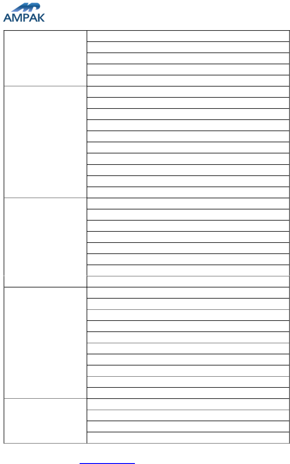
Conditions : VBAT=3.6V ; VDDIO=3.3V ; Temp:25°C
Feature
Description
General Specification
Bluetooth Standard
Bluetooth V4.1 of 1, 2 and 3 Mbps.
Antenna Reference
Small antennas with 0~2 dBi peak gain
Frequency Band
2402 MHz ~ 2480 MHz
Number of Channels
79 channels
Modulation
FHSS, GFSK, DPSK, DQPSK
RF Specification
Min.
Typical.
Max.
Output Power (Class 1.5)
7 dBm
Output Power (Class 2)
2 dBm
Sensitivity @ BER=0.1%
for GFSK (1Mbps)
-80 dBm
Sensitivity @ BER=0.01%
for π/4-DQPSK (2Mbps)
-80 dBm
Sensitivity @ BER=0.01%
for 8DPSK (3Mbps)
-78 dBm
Maximum Input Level
GFSK (1Mbps):-20dBm
π/4-DQPSK (2Mbps) :-20dBm
8DPSK (3Mbps) :-20dBm
AMPAK Technology Inc. www.ampak.com.tw Proprietary & Confidential Information
Doc. NO:
17
7. Pin Assignments
7.1 Pin Map
< TOP VIEW >
7.2 Pin Definition
NO
Name
Type
Description
1
NC
-
No connect
2
NC
-
No connect
3
JTAG_TDI_GPIO4
I
1: SPROM is present
0: SPROM is absent (default). Applicable in PCIe HOST mode

AMPAK Technology Inc. www.ampak.com.tw Proprietary & Confidential Information
Doc. NO:
18
4
NC
-
No connect
5
3V3_VBAT
I
VBAT system power supply input
6
GND
-
Ground connections
7
JTAG_TDO_GPIO_5
I/O
GPIO_5
8
GPIO_8
I/O
SDIO and PCIe interface strapping option
9
GPIO_9
I/O
SDIO and PCIe interface strapping option
10
NC
-
No connect
11
JTAG_TRST_N_COEX0_
GPIO_6
I/O
GPIO_6
12
JTAG_TCK_COEX1_
GPIO_2
I/O
GPIO_2
13
JTAG_TMS_COEX2_
GPIO_3
I/O
GPIO_3
14
NC
-
No connect
15
NC
-
No connect
16
NC
-
No connect
17
GND
-
Ground connections
18
NC
-
No connect
19
NC
-
No connect
20
GND
-
Ground connections
21
NC
-
No connect
22
NC
-
No connect
23
GND
-
Ground connections
24
BT_DEV_WAKE
I/O
Bluetooth DEV_WAKE
25
NC
-
No connect
26
GND
-
Ground connections
27
SLP_CLK
I
External sleep clock input (32.768KHz)
28
WL_RFDISABLE_L_GPIO1
I/O
WL_DEV_WAKE
29
PCIE_WAKEn
O
PCIe wake signal
30
PCIE_CLKREQn
I/O
PCIe clock request
31
PCIE_PERSTn
I
PCIe host indication to reset the device
32
GND
-
Ground connections
33
PCIE_RCLK_N
I
PCI Express differential clock input-Negative
34
PCIE_RCLK_P
I
PCI Express differential clock input-Positive
35
GND
-
Ground connections
36
PCIE_TX_N
O
PCI Express transmit data-Negative
37
PCIE_TX_P
O
PCI Express transmit data-Positive

AMPAK Technology Inc. www.ampak.com.tw Proprietary & Confidential Information
Doc. NO:
19
38
GND
-
Ground connections
39
PCIE_RX_N
I
PCI Express receive data-Negative
40
PCIE_RX_P
I
PCI Express receive data-Positive
41
GND
-
Ground connections
42
NC
-
No connect
43
BT_I2S_WS
I/O
I2S data command line
44
VIO_SD
I
Digital I/O SDIO power supply
45
SDIO_RESET_L_
WL_REG_ON
I
Used by PMU to power up or power down the internal
module regulators used by the WLAN section.
46
SDIO_WAKE_L_GPIO_0
I
WL_HOST_WAKE
47
SDIO_DATA3
I/O
SDIO data line bit3
48
SDIO_DATA2
I/O
SDIO data line bit2
49
SDIO_DATA1
I/O
SDIO data line bit1
50
SDIO_DATA0
I/O
SDIO data line bit0
51
SDIO_CMD
I/O
SDIO command/response
52
SDIO_CLK
I
SDIO clock input
53
BT_HOST_WAKE
O
Bluetooth HOST_WAKE
54
UART_CTS
I
UART_CTS
55
UART_SOUT
O
UART_SOUT
56
UART_SIN
I
UART_SIN
57
UART_RTS
O
UART_RTS
58
PCM_SYNC
I/O
PCM sync
59
PCM_IN
I
PCM data in
60
PCM_OUT
O
PCM data out
61
PCM_CLK
I/O
PCM bus clock
62
GND
-
Ground connections
63
BT_ENABLE
I
Used by PMU to power up or power down the internal
module regulators used by the Bluetooth section.
64
BT_I2S_DO_
BT_LED
O
I2S data line output
It can be used as BT_LED
65
WL_LED_GPIO_7
O
It can be used as WL_LED
66
BT_I2S_DI
I
I2S data line input
67
BT_I2S_CLK
I/O
I2S data line clock
68
GND
-
Ground connections
69
USB_DM
I/O
USB serial differential data Negative
70
USB_DP
I/O
USB serial differential dataPositive
71
GND
-
Ground connections

AMPAK Technology Inc. www.ampak.com.tw Proprietary & Confidential Information
Doc. NO:
20
72
3V3_USB
I
3.3V power supply
73
VIO
I
Digital I/O power supply
74
GND
-
Ground connections
75
GND
-
Ground connections
76
GND
-
Ground connections
77
GND
-
Ground connections
78
GND
-
Ground connections
79
GND
-
Ground connections
80
GND
-
Ground connections
81
GND
-
Ground connections
82
GND
-
Ground connections
83
GND
-
Ground connections
84
GND
-
Ground connections
85
GND
-
Ground connections
86
GND
-
Ground connections
87
GND
-
Ground connections
88
GND
-
Ground connections
89
GND
-
Ground connections
90
GND
-
Ground connections
91
GND
-
Ground connections
92
GND
-
Ground connections
93
GND
-
Ground connections
94
GND
-
Ground connections
95
GND
-
Ground connections
96
GND
-
Ground connections
G1
GND
-
Ground connections
G2
GND
-
Ground connections
G3
GND
-
Ground connections
G4
GND
-
Ground connections
G5
GND
-
Ground connections
G6
GND
-
Ground connections
G7
GND
-
Ground connections
G8
GND
-
Ground connections
G9
GND
-
Ground connections
G10
GND
-
Ground connections
G11
GND
-
Ground connections
G12
GND
-
Ground connections
AMPAK Technology Inc. www.ampak.com.tw Proprietary & Confidential Information
Doc. NO:
21
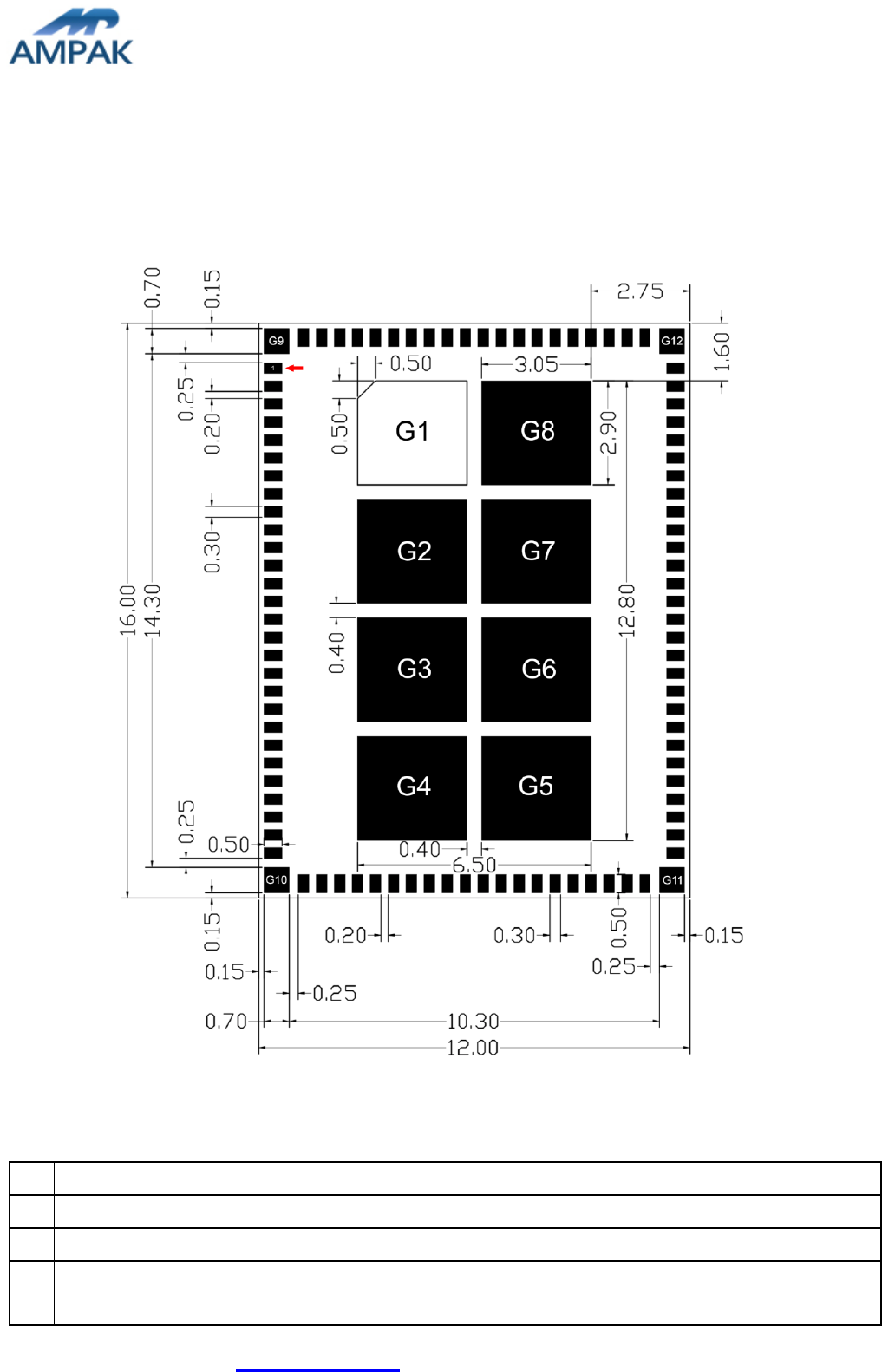
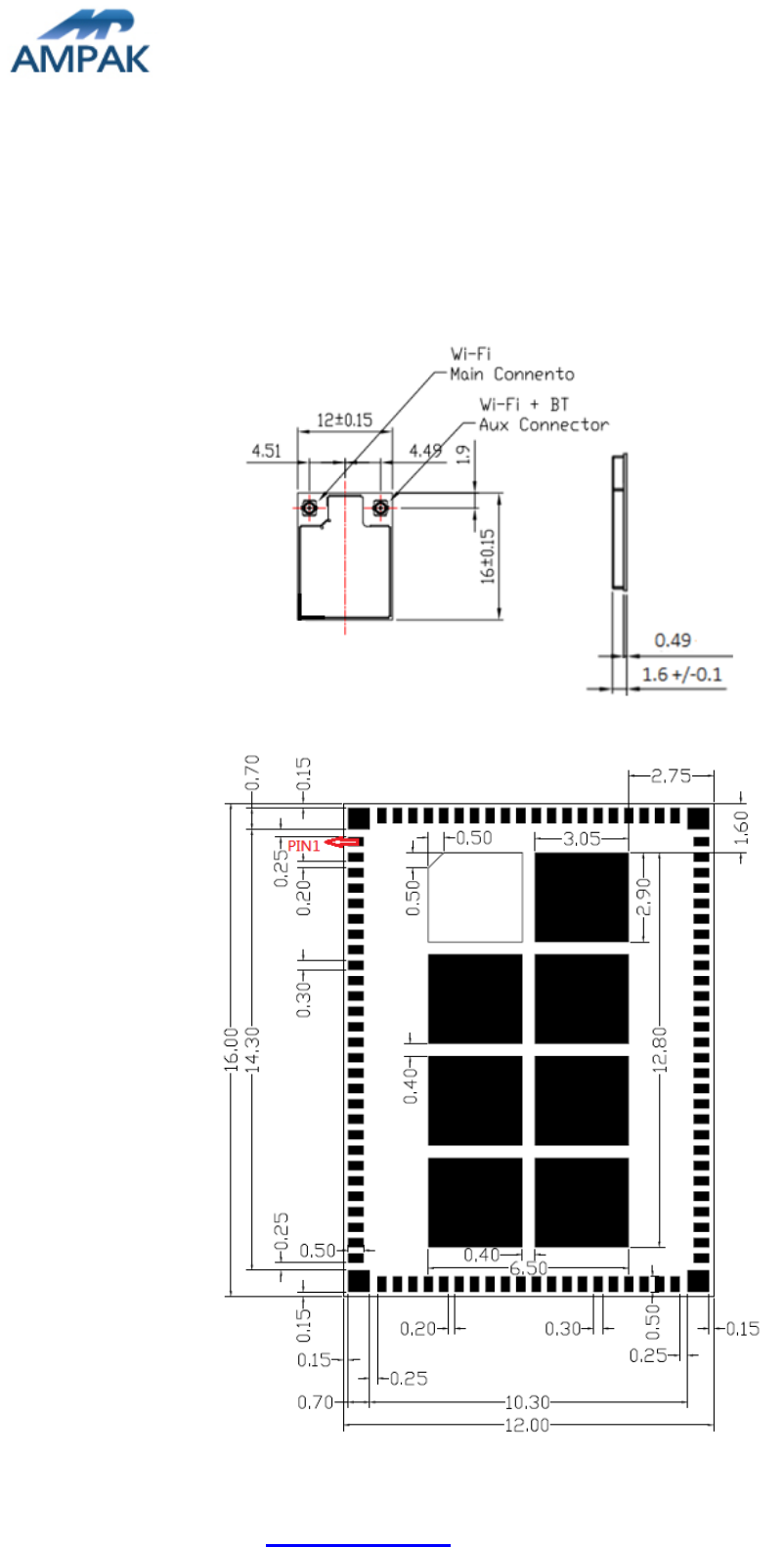
8. Dimensions
8.1 Physical Dimensions
(Unit: mm)
< TOP VIEW >
TOP VIEW >
AMPAK Technology Inc. www.ampak.com.tw Proprietary & Confidential Information
Doc. NO:
22
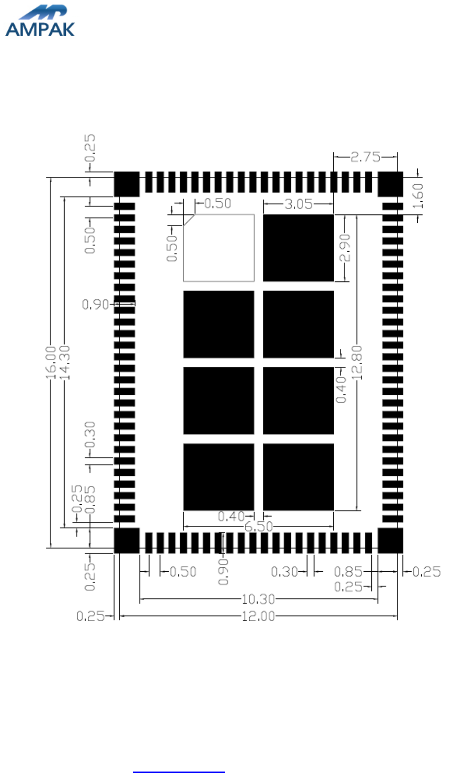
8.2 Layout Recommendation
(Unit: mm)
< TOP VIEW >
AMPAK Technology Inc. www.ampak.com.tw Proprietary & Confidential Information
Doc. NO:
24
9. External clock reference
External LPO signal characteristics
Parameter
Specification
Units
Nominal input frequency
32.768
kHz
Frequency accuracy
30
ppm
Duty cycle
30 - 70
%
Input signal amplitude
1600 to 3300
mV, p-p
Signal type
Square-wave or sine-wave
-
Input impedance
>100k
<5
pF
Clock jitter (integrated over 300Hz – 15KHz)
<1
Hz
Output high voltage
0.7Vio - Vio
V
9.1 SDIO Pin Description
The module supports SDIO version 3.0 for all 1.8V 4-bit UHSI speeds: SDR50(100
Mbps),SDR104(208MHz) and DDR50(50MHz, dual rates) in addition to the 3.3V default
speed(25MHz) and high speed (50 MHz). It has the ability to stop the SDIO clock and map
the interrupt signal into a GPIO pin. This ‘out-of-band’ interrupt signal notifies the host when
the WLAN device wants to turn on the SDIO interface. The ability to force the control of the
gated clocks from within the WLAN chip is also provided.
Function 0 Standard SDIO function (Max BlockSize / ByteCount = 32B)
Function 1 Backplane Function to access the internal System On Chip (SOC)
address space (Max BlockSize / ByteCount = 64B)
Function 2 WLAN Function for efficient WLAN packet transfer through DMA (Max
BlockSize/ByteCount=512B)
SDIO Pin Description
SD 4-Bit Mode
DATA0
Data Line 0
DATA1
Data Line 1 or Interrupt
DATA2
Data Line 2 or Read Wait
DATA3
Data Line 3
CLK
Clock
CMD
Command Line
AMPAK Technology Inc. www.ampak.com.tw Proprietary & Confidential Information
Doc. NO:
25
10. Host Interface Timing Diagram
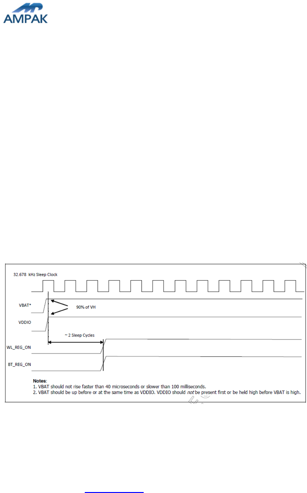
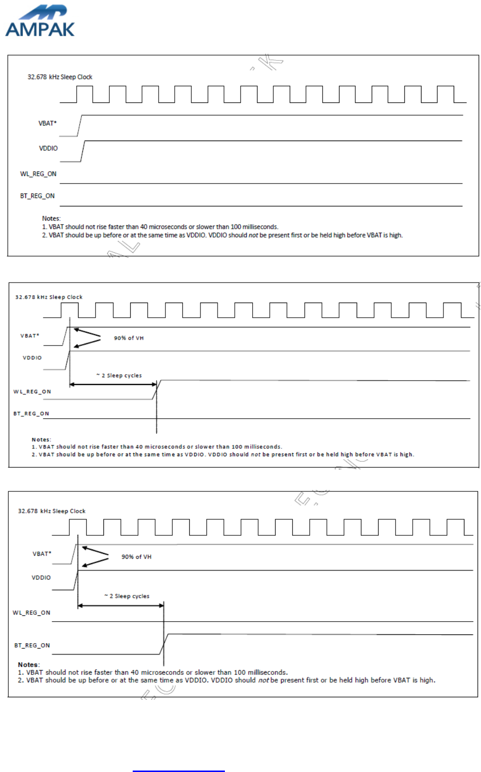
10.1 Power-up Sequence Timing Diagram
The module has signals that allow the host to control power consumption by enabling or
disabling the Bluetooth, WLAN and internal regulator blocks. These signals are described
below.
Additionally, diagrams are provided to indicate proper sequencing of the signals for carious
operating states. The timing value indicated are minimum required values: longer delays are
also acceptable.
※ WL_REG_ON: Used by the PMU to power up or power down the internal
regulators used by the WLAN section. When this pin is high, the regulators are
enabled and the WLAN section is out of reset. When this pin is low the WLAN
section is in reset.
※ BT_REG_ON: Used by the PMU to power up or power down the internal regulators
used by the BT section. Low asserting reset for Bluetooth. This pin has no effect on
WLAN and does not control any PMU functions. This pin must be driven high or low
(not left floating).
WLAN=ON, Bluetooth=ON
AMPAK Technology Inc. www.ampak.com.tw Proprietary & Confidential Information
Doc. NO:
26
WLAN=OFF, Bluetooth=OFF
WLAN=ON, Bluetooth=OFF
WLAN=OFF, Bluetooth=ON
AMPAK Technology Inc. www.ampak.com.tw Proprietary & Confidential Information
Doc. NO:
27
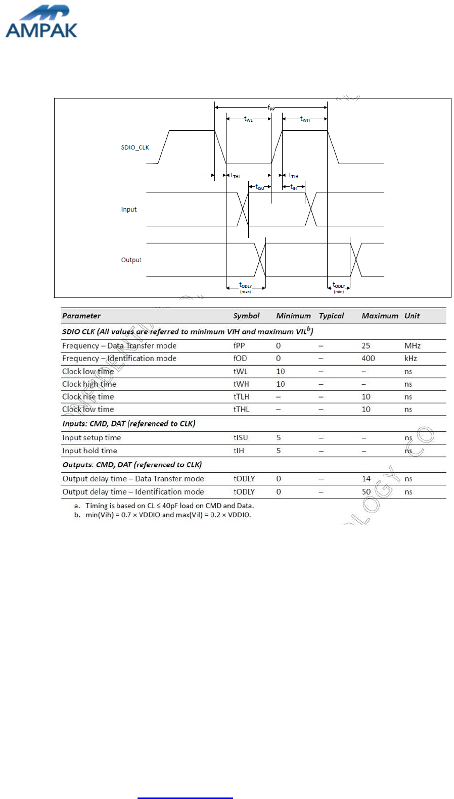
10.2 SDIO Default Mode Timing Diagram
AMPAK Technology Inc. www.ampak.com.tw Proprietary & Confidential Information
Doc. NO:
28
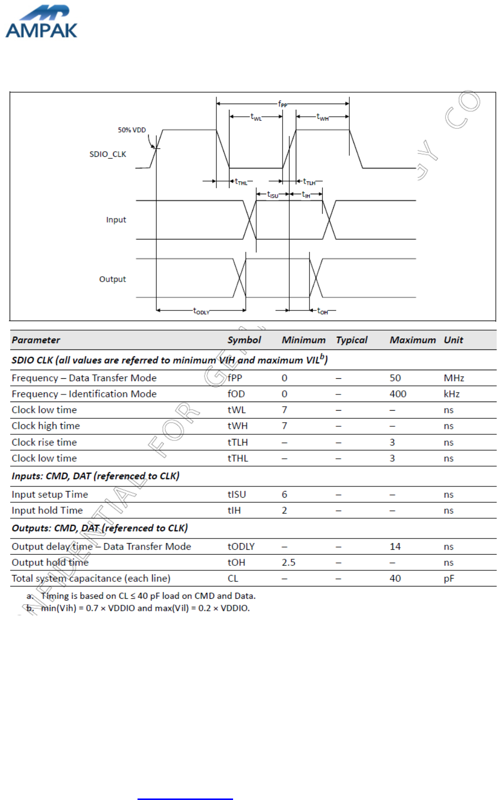
10.3 SDIO High Speed Mode Timing Diagram
AMPAK Technology Inc. www.ampak.com.tw Proprietary & Confidential Information
Doc. NO:
29
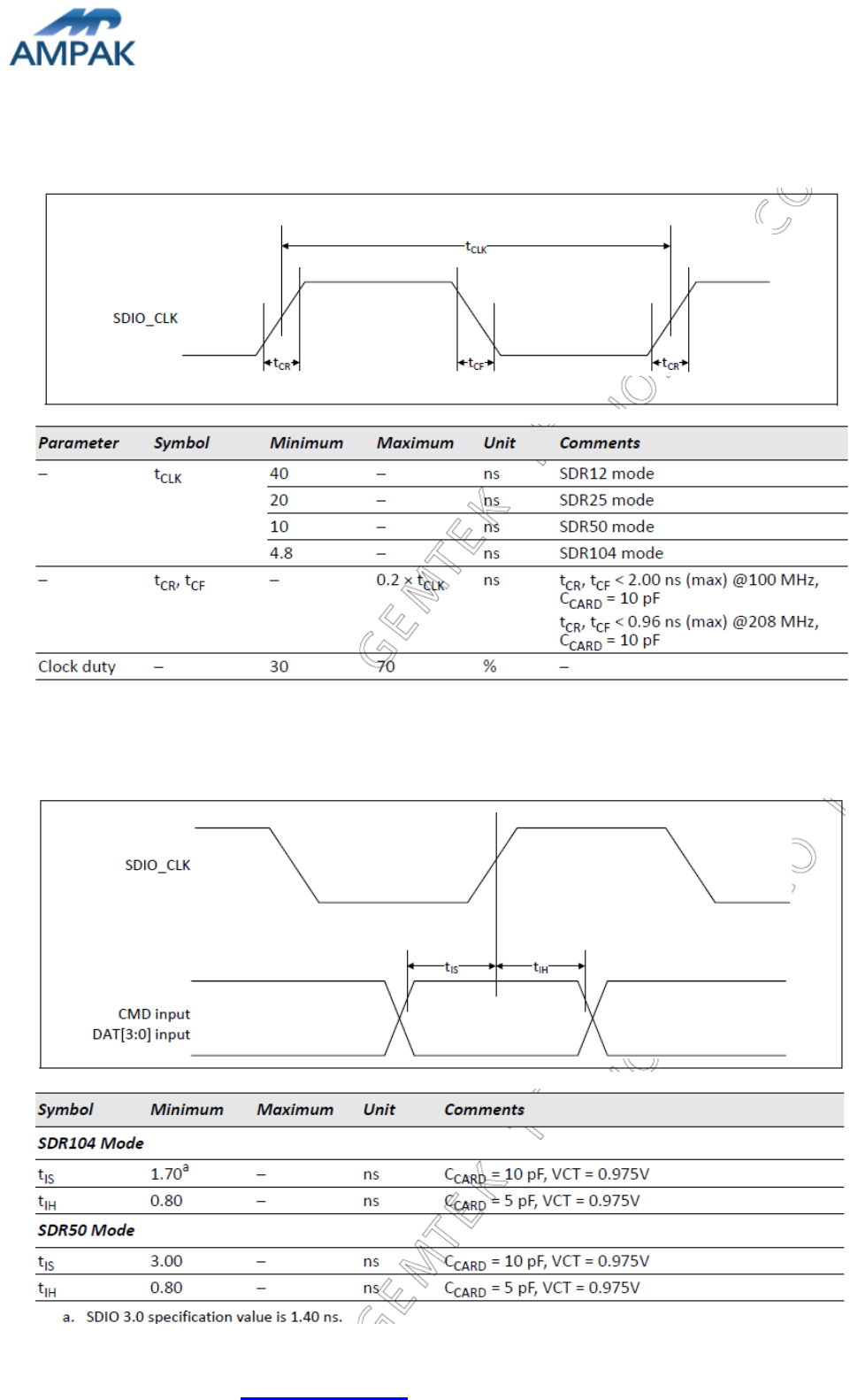
10.4 SDIO Bus Timing Specifications in SDR Modes
Clock timing(SDR Modes)
Card Input timing (SDR Modes)
AMPAK Technology Inc. www.ampak.com.tw Proprietary & Confidential Information
Doc. NO:
30
Card output timing (SDR Modes up to 100MHz)
Card output timing (SDR Modes 100MHz to 208MHz)
AMPAK Technology Inc. www.ampak.com.tw Proprietary & Confidential Information
Doc. NO:
31
10.5 SDIO Bus Timing Specifications in DDR50 Mode
Data Timing
AMPAK Technology Inc. www.ampak.com.tw Proprietary & Confidential Information
Doc. NO:
32
11. Recommended Reflow Profile
Referred to IPC/JEDEC standard.
Peak Temperature : <250°C
Number of Times : 2 times
2.5℃/sec
2.5°C/sec
40~70 sec
250℃
AMPAK Technology Inc. www.ampak.com.tw Proprietary & Confidential Information
Doc. NO:
33
12. Package Information
12.1Label
Label A Anti-static and humidity notice
Label B MSL caution / Storage Condition
Label C Inner box label .
Label D Carton box label .
AMPAK Technology Inc. www.ampak.com.tw Proprietary & Confidential Information
Doc. NO:
34
12.2 Dimension
AMPAK Technology Inc. www.ampak.com.tw Proprietary & Confidential Information
Doc. NO:
35
A
B
C
Humidity indicator
Desiccant
C
D
AMPAK Technology Inc. www.ampak.com.tw Proprietary & Confidential Information
Doc. NO:
36
12.3 MSL Level / Storage Condition
※NOTE : Accumulated baking time should not exceed 96hrs