Acer orporated T77H389 Dual band WiFi LGA Module User Manual
Acer Incorporated Dual band WiFi LGA Module
Contents
- 1. user manual
- 2. User Manual
- 3. Users Manual Regulatory Info
user manual

COMPANY CONFIDENTIAL
BCM4330 WLAN+BT Combo Module
(Foxconn T77H389.00)
Product Specification
Rev 3.0
Prepared by
Reviewed by
Approved by
Sarah Liu
Ai-Ning Song
Chang-Fu Lin
Index

COMPANY CONFIDENTIAL
1. REVISION HISTORY ................................................................................................................................................... 3
2. INTRODUCTION .......................................................................................................................................................... 4
2.1 SCOPE ...................................................................................................................................................................... 4
2.2 FUNCTION ................................................................................................................................................................. 4
3. PRODUCT SPECIFICATION ..................................................................................................................................... 5
3.1 HARDWARE CHARACTERISTIC ................................................................................................................................. 5
3.2 HARDWARE ARCHITECTURE .................................................................................................................................... 5
3.3 ELECTRICAL SPECIFICATION .................................................................................................................................... 5
3.4 WLAN RF CHARACTERISTICS ................................................................................................................................. 6
3.4.1 IEEE802.11b .................................................................................................................................................. 6
3.4.2 IEEE802.11g .................................................................................................................................................. 7
3.4.3 IEEE802.11n HT20(2.4GHz) ....................................................................................................................... 8
3.4.5 IEEE802.11a .................................................................................................................................................. 9
3.4.6 IEEE802.11n HT20 (5GHz) ....................................................................................................................... 10
3.5 BLUETOOTH STANDARD SPECIFICATIONS ............................................................................................................. 11
3.6 LGA PIN DEFINITION .............................................................................................................................................. 11
4. SOFTWARE REQUIREMENT.................................................................................................................................. 13
5. REGULATORY ........................................................................................................................................................... 13
6. ENVIRONMENTAL REQUIREMENTS AND SPECIFICATIONS ....................................................................... 13
6.1 TEMPERATURE ....................................................................................................................................................... 13
6.2 PCB BENDING ........................................................................................................................................................ 13
6.3 HANDLING ENVIRONMENT ....................................................................................................................................... 14
6.4 STORAGE CONDITION ............................................................................................................................................. 14
6.5 BAKING CONDITION ................................................................................................................................................ 14
6.6 SOLDERING AND REFLOW CONDITION .................................................................................................................... 14

COMPANY CONFIDENTIAL
1. Revision History
Date
Change Note
REV Note
2011-12-26
Initial release
1.0
2012-04-16
1. Update block diagram in 3.2.
2. Update Electrical Specification in 3.3.
3. Update WLAN RF Characteristics in 3.4.
4. Update Bluetooth Standard Specifications in 3.5.
5. Change LGA G6 pin definition in 3.6.
6. Update mechanical drawing.
5. Update schematic drawing.
6. update PCB layout.
2.0
2012-06-18
1. Update WLAN RF characteristics in 3.4.
2. Update Bluetooth standard specifications in 3.5.
3. Update schematic.
3.0

COMPANY CONFIDENTIAL
2. Introduction
Project Name: 802.11abgn (1X1) + BT4.0 combo module
This documentation describes the product specification of the WLAN+BT combo Module. WLAN is Compliant
with IEEE Std. 802.11b-1999, IEEE Std. 802.11g-2003 and IEEE Std. 802.11n-2009, Bluetooth is compliant
with Bluetooth 4.0+HS. It is a confidential document of Foxconn.
* For b/g/n and a/b/g/n module, Foxconn HW/FW are the same, platform use different firmware and
driver to enable or disable 5GHz
2.1 Scope
This combo Module combines WLAN, Bluetooth in one module, the WLAN is available in the 2.4GHz
and 5GHz band, it is compatible with the IEEE 802.11 a/b/g standard and the 802.11n standard. It allow
user to switch to different vendors’ Access Points through the wireless networks and to prevent from
eavesdropping. The 802.11 a/g data rate provides for 54, 48, 36, 24, 18, 12, 9, 6Mbps, 802.11b data
rate provides for 11, 5.5, 2, 1 Mbps, it can also support 11n high data rate up to MCS7(HT20) with PHY
data rate to 72Mbps. Bluetooth is compliant to Core Specification version 4.0.
2.2 Function
Single stream 802.11n support for 20MHz channels provide PHY layer rates up to 72Mbps.
Bluetooth supports Class 1 and Class 2 output power.
Provides a small form factor solution and ultra low power consumption to support low cost requirement.
Host interface supports:
WLAN: SDIO;
BT data: UART
BT digital audio: PCM

COMPANY CONFIDENTIAL
3. Product Specification
3.1 Hardware Characteristic
Form factor 14.5mmx14.5mm LGA
Host Interface WLAN: SDIO
BT: UART for data, PCM for Audio
PCB 6-layer HDI design
RF connector Two MHF RF connector on module
3.2 Hardware Architecture
The WLAN+BT combo module is designed base on BROADCOM BCM4330 chip, the Broadcom
BCM4330 is a highly integrated single chip solution for single stream dual-band WLAN and BT4.0, use
two RF connector with one for antenna diversity, a 26MHz crystal is used for reference clock
generation, see the block diagram as below:
3.3 Electrical Specification
Absolute Maximum Ratings
These specification indicate levels where permanent damage to the device can occur. Functional
operation is not guaranteed under these conditions. Operation at absolute maximum conditions for extended
can adversely affect long-term reliability of the device.
Recommended Operating Condition
Element
Symbol
Value
Unit
Minimum
Typical
Maximum
DC supply voltage for the device
VBAT_3.3V
3.0
3.3
3.6
V
VDDIO for WL_VDDIO and BT_VDDIO
VIO_1.8V
1.2
1.8
2.9
V
Function operation is not guaranteed outside this limit, and operation outside this limit for extended
periods can adversely affect long-term reliability of the device.
Remark:
VBAT_3.3V range is restricted by FEM SE5007BT.
Rating
Symbol
Value
Unit
DC supply voltage for the device
VBAT_3.3V
-0.3 to 3.6
V
VDDIO
VIO
-0.5 to 2.98
V
COMPANY CONFIDENTIAL
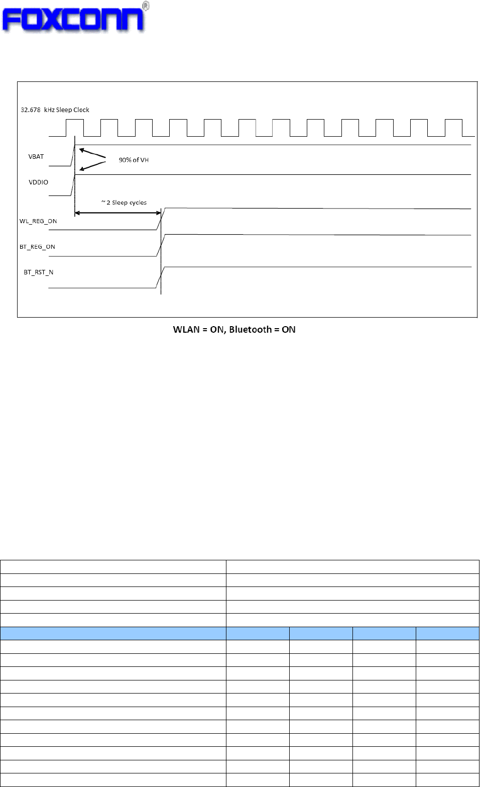
Power-Up Sequence Timing
Current Consumption
TBD
* Will be updated after EDVT testing.
Product ID Definition
Vendor ID: 0x14e4
Device ID: 0x4360
3.4 WLAN RF Characteristics
3.4.1 IEEE802.11b
Items
Contents
Specification
IEEE802.11b
Mode
DSSS / CCK
Channel
CH1 to CH13,CH14
Data rate
1, 2, 5.5, 11Mbps
-TX Characteristics-
Min.
Typ.
Max.
Unit
1. Power Levels
1) Target Power@1Mbps
13
15
17
dBm
2) Target Power@2Mbps
13
15
17
dBm
3) Target Power@5.5Mbps
13
15
17
dBm
4) Target Power@11Mbps
13
15
17
dBm
2. Spectrum Mask @18dBm
1) fc-33MHz < f < fc-22MHz
-
-
-50
dBr
2) fc-22MHz < f < fc-11MHz
-
-
-30
dBr
3) fc+11MHz < f < fc+22MHz
-
-
-30
dBr
4) fc+22MHz < f < fc+33MHz
-
-
-50
dBr
3. Frequency Error
-15
-
+15
ppm
COMPANY CONFIDENTIAL
4.Modulation Accuracy(EVM)@18dBm
1) 1Mbps
-
-
-9.1
dB
2) 2Mbps
-
-
-9.1
dB
3) 5.5Mbps
-
-
-9.1
dB
4) 11Mbps
-
-
-9.1
dB
-RX Characteristics-
Min.
Typ.
Max.
Unit
5. Minimum Input Level Sensitivity
1) 1Mbps (FER≦8%)
-
-91
-
dBm
2) 2Mbps (FER≦8%)
-
-90
-
dBm
3) 5.5Mbps (FER≦8%)
-
-87
-
dBm
4) 11Mbps (FER≦8%)
-
-85
-
dBm
6. Maximum Input Level
-10
-7
-
dBm
-Spurious Emission-
Min.
Typ.
Max.
Unit
FCC(30MHz- 1GHz)
-
-
-41.3
dBm
FCC Average(1GHz – 12.75GHz)
-
-
-41.3
dBm
3.4.2 IEEE802.11g
Items
Contents
Specification
IEEE802.11g
Mode
OFDM
Channel
CH1 to CH13
Data rate
6, 9, 12, 18, 24, 36, 48, 54Mbps
- TX Characteristics -
Min.
Typ.
Max.
Unit
1. Power Levels
1) Target Power@6Mbps
11
13
15
dBm
2) Target Power@9Mbps
11
13
15
dBm
3) Target Power@12Mbps
11
13
15
dBm
4) Target Power@18Mbps
11
13
15
dBm
5) Target Power@24Mbps
11
13
15
dBm
6) Target Power@36Mbps
11
13
15
dBm
7) Target Power@48Mbps
11
13
15
dBm
8) Target Power@54Mbps
11
13
15
dBm
2. Spectrum Mask @16dBm
1) at fc +/- 11MHz
-
-
-20
dBr
2) at fc +/- 20MHz
-
-
-28
dBr
3) at fc > +/-30MHz
-
-
-40
dBr
3. Frequency Error
-15
-
+15
ppm
4. Constellation Error(EVM)@16dBm
1) 6Mbps
-
-
-5
dB
2) 9Mbps
-
-
-8
dB
3) 12Mbps
-
-
-10
dB
4) 18Mbps
-
-
-13
dB
5) 24Mbps
-
-
-16
dB
6) 36Mbps
-
-
-19
dB
7) 48Mbps
-
-
-22
dB
8) 54Mbps
-
-
-25
dB
- RX Characteristics -
Min.
Typ.
Max.
Unit
5. Minimum Input Level Sensitivity
1) 6Mbps (PER < 10%)
-
-88
-
dBm
2) 9Mbps (PER < 10%)
-
-86
-
dBm
3) 12Mbps (PER < 10%)
-
-85
-
dBm
4) 18Mbps (PER < 10%)
-
-84
-
dBm
5) 24Mbps (PER < 10%)
-
-82
-
dBm
6) 36Mbps (PER < 10%)
-
-78
-
dBm
7) 48Mbps (PER < 10%)
-
-74
-
dBm
8) 54Mbps (PER < 10%)
-
-72
-
dBm
COMPANY CONFIDENTIAL
6. Maximum Input Level (PER < 10%)
-20
-7
-
dBm
-Spurious Emission-
Min.
Typ.
Max.
Unit
FCC(30MHz- 1GHz)
-
-
-41.3
dBm
FCC Average(1GHz – 12.75GHz)
-
-
-41.3
dBm
3.4.3 IEEE802.11n HT20(2.4GHz)
Items
Contents
Specification
IEEE802.11n HT20
Mode
OFDM
Channel
CH1 to CH13
Data rate (MCS index)
MCS0~MCS7
- TX Characteristics -
Min.
Typ.
Max.
Unit
1. PowerLevels
1) Target Power@MCS0
10
12
14
dBm
2) Target Power@ MCS1
10
12
14
dBm
3) Target Power@ MCS2
10
12
14
dBm
4) Target Power@ MCS3
10
12
14
dBm
5) Target Power@ MCS4
10
12
14
dBm
6) Target Power@ MCS5
10
12
14
dBm
7) Target Power@ MCS6
10
12
14
dBm
8) Target Power@ MCS7
10
12
14
dBm
2. Spectrum Mask @15dBm
1) at fc +/- 11MHz
-
-
-20
dBr
2) at fc +/- 20MHz
-
-
-28
dBr
3) at fc > +/-30MHz
-
-
-45
dBr
3. Frequency Error
-15
-
+15
ppm
4. Constellation Error(EVM)@15dBm
1) MCS0
-
-
-5
dB
2) MCS1
-
-
-10
dB
3) MCS2
-
-
-13
dB
4) MCS3
-
-
-16
dB
5) MCS4
-
-
-19
dB
6) MCS5
-
-
-22
dB
7) MCS6
-
-
-25
dB
8) MCS7
-
-
-28
dB
- RX Characteristics -
Min.
Typ.
Max.
Unit
5. Minimum Input Level Sensitivity
1) MCS0 (PER < 10%)
-
-85
-
dBm
2) MCS1 (PER < 10%)
-
-84
-
dBm
3) MCS2 (PER < 10%)
-
-82
-
dBm
4) MCS3 (PER < 10%)
-
-80
-
dBm
5) MCS4 (PER < 10%)
-
-77
-
dBm
6) MCS5 (PER < 10%)
-
-73
-
dBm
7) MCS6 (PER < 10%)
-
-71
-
dBm
8) MCS7 (PER < 10%)
-
-69
-
dBm
6. Maximum Input Level (PER < 10%)
-20
-7
-
dBm
-Spurious Emission-
Min.
Typ.
Max.
Unit
FCC(30MHz- 1GHz)
-
-
-41.3
dBm
FCC Average(1GHz – 12.75GHz)
-
-
-41.3
dBm
COMPANY CONFIDENTIAL
3.4.5 IEEE802.11a
Items
Contents
Specification
IEEE802.11a
Mode
OFDM
Channel
lower band:5.15GHz~5.25GHz
middle band:5.25GHz~5.35GHz
upper band:5.745GHz~5.805GHz
Data rate
6, 9, 12, 18, 24, 36, 48, 54Mbps
- TX Characteristics -
Min.
Typ.
Max.
Unit
1. Power Levels
Low Band
12.5
14
15.5
dBm
Middle Band
12.5
14
15.5
dBm
Upper Band
12.5
14
15.5
dBm
2. Spectrum Mask @ Type power
1) at fc +/- 11MHz
-
-
-20
dBr
2) at fc +/- 20MHz
-
-
-28
dBr
3) at fc > +/-30MHz
-
-
-40
dBr
3. Frequency Error
-15
-
+15
ppm
4. Constellation Error(EVM)@ Type power
1) 6Mbps
-
-
-5
dB
2) 9Mbps
-
-
-8
dB
3) 12Mbps
-
-
-10
dB
4) 18Mbps
-
-
-13
dB
5) 24Mbps
-
-
-16
dB
6) 36Mbps
-
-
-19
dB
7) 48Mbps
-
-
-22
dB
8) 54Mbps
-
-
-25
dB
- RX Characteristics -
Min.
Typ.
Max.
Unit
5. Minimum Input Level Sensitivity
1) 6Mbps (PER < 10%)
-
-90
-
dBm
2) 9Mbps (PER < 10%)
-
-89
-
dBm
3) 12Mbps (PER < 10%)
-
-88
-
dBm
4) 18Mbps (PER < 10%)
-
-86
-
dBm
5) 24Mbps (PER < 10%)
-
-84
-
dBm
6) 36Mbps (PER < 10%)
-
-81
-
dBm
7) 48Mbps (PER < 10%)
-
-77
-
dBm
8) 54Mbps (PER < 10%)
-
-75
-
dBm
6. Maximum Input Level (PER < 10%)
-30
-24
-
dBm
-Spurious Emission-
Min.
Typ.
Max.
Unit
FCC(30MHz- 1GHz)
-
-
-41.3
dBm
FCC Average(1GHz – 12.75GHz)
-
-
-41.3
dBm

COMPANY CONFIDENTIAL
3.4.6 IEEE802.11n HT20 (5GHz)
* The performance will be updated after EDVT testing.
Items
Contents
Specification
IEEE802.11n HT20
Mode
OFDM
Channel
low band:5.15GHz~5.25GHz
middle band:5.25GHz~5.35GHz
upper band:5.5GHz~5.825GHz
Data rate (MCS index)
MCS0~MCS7
- TX Characteristics -
Min.
Typ.
Max.
Unit
1. Power Levels
Low Band
11.5
13
14.5
dBm
Middle Band
11.5
13
14.5
dBm
Upper Band
11.5
13
14.5
dBm
2. Spectrum Mask @Type power
1) at fc +/- 11MHz
-
-
-20
dBr
2) at fc +/- 20MHz
-
-
-28
dBr
3) at fc > +/-30MHz
-
-
-45
dBr
3. Frequency Error
-15
-
+15
ppm
4. Constellation Error(EVM)@Type power
1) MCS0
-
-
-5
dB
2) MCS1
-
-
-10
dB
3) MCS2
-
-
-13
dB
4) MCS3
-
-
-16
dB
5) MCS4
-
-
-19
dB
6) MCS5
-
-
-22
dB
7) MCS6
-
-
-25
dB
8) MCS7
-
-
-28
dB
- RX Characteristics -
Min.
Typ.
Max.
Unit
5. Minimum Input Level Sensitivity
1) MCS0 (PER < 10%)
-
-89
-
dBm
2) MCS1 (PER < 10%)
-
-87
-
dBm
3) MCS2 (PER < 10%)
-
-85
-
dBm
4) MCS3 (PER < 10%)
-
-83
-
dBm
5) MCS4 (PER < 10%)
-
-79
-
dBm
6) MCS5 (PER < 10%)
-
-75
-
dBm
7) MCS6 (PER < 10%)
-
-73
-
dBm
8) MCS7 (PER < 10%)
-
-72
-
dBm
6. Maximum Input Level (PER < 10%)
-30
-
-
dBm
- RX Characteristics -
Min.
Typ.
Max.
Unit
FCC(30MHz- 1GHz)
-
-
-41.3
dBm
FCC Average(1GHz – 12.75GHz)
-
-
-41.3
dBm
COMPANY CONFIDENTIAL
3.5 Bluetooth Standard Specifications
Bluetooth Core Specification version 4.0:
Host interface: UART, baud rates up to 4Mbps
Support all Bluetooth 4.0+HS packet types.
Operating frequency range: 2400MHz ~2483.5MHz
Modulation type:
Basic rate 1Mbps: GFSK,
Enhanced data rate 2Mbps: DQPSK
Enhanced data rate 3Mbps: 8DPSK
Remark: BT power level can be changed according to customer’s request by modifying hcd file.
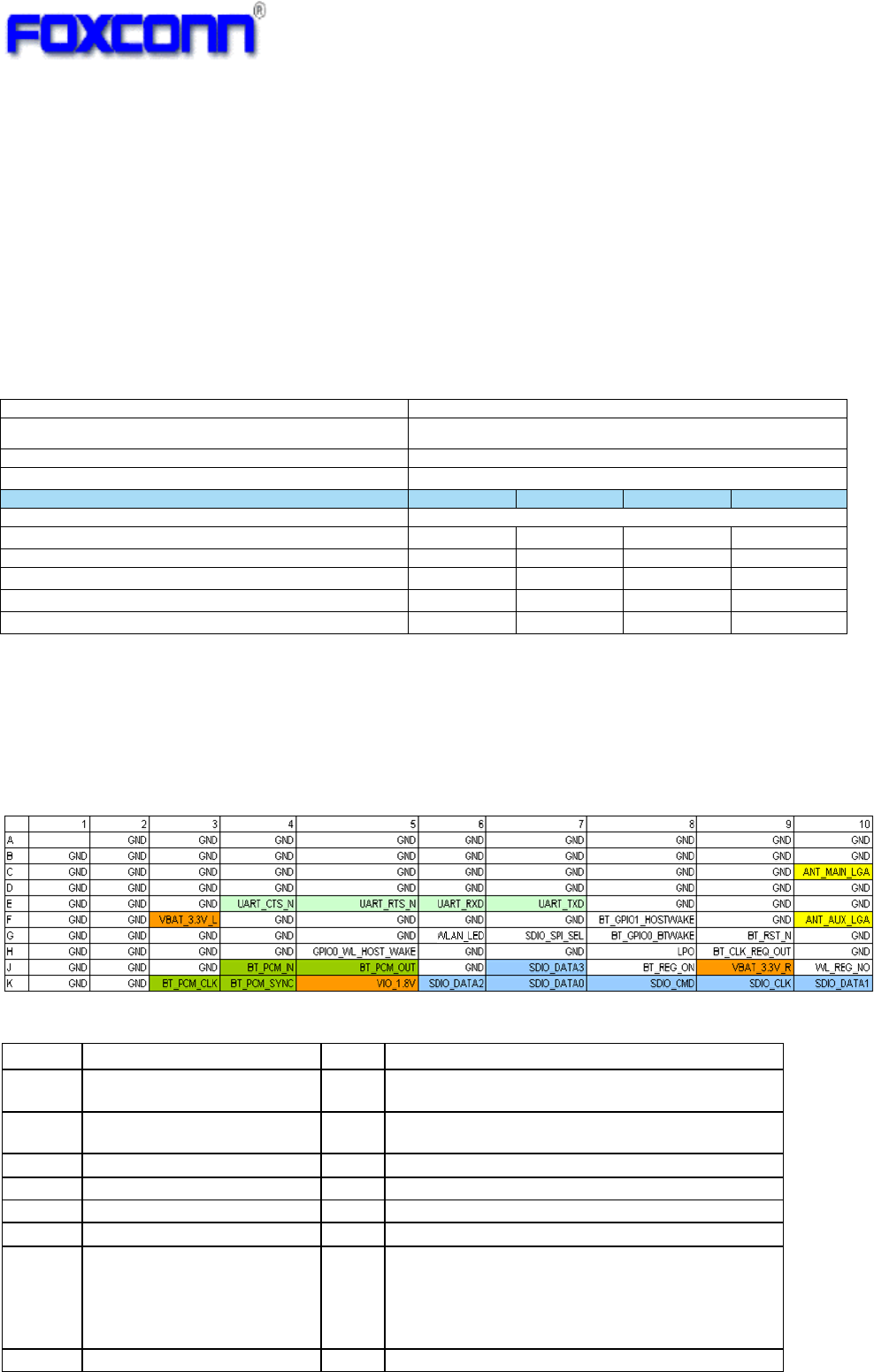
3.6 LGA Pin Definition
Bottom View
Pin No.
Pin Name
Type
Description
C10
ANT_MAIN_LGA
I/O
Reserved LGA pin for connecting main antenna on
mother board
F10
ANT_AUX_LGA
I/O
Reserved LGA pin for connecting aux antenna on
mother board
E4
UART_CTS_N
I
UART clear to Send, active low (for BT data)
E5
UART_RTS_N
O
UART request to Send, active low (for BT data)
E6
UART_RXD
I
UART signal input
E7
UART_TXD
O
UART signal output
F3
VBAT_3.3V_L
I
Main power supply for the module, (3.3V+/-10%,
together with pin J9 to
supply the module ), reserve 500mA current
consumption for this pin,
need external 10uF decoupling cap
F8
BT_GPIO1_HOSTWAKE
O
Signal from module to host to require Host wake up
Items
Contents
Specification
BT4.0+EDR
Frequency range
2.4G~2.4835G
Data rate
1Mbps, 2Mbps, 3Mbps
- TX Characteristics -
Min.
Typ.
Max.
Unit
1. Power Levels
BT Output Power
0
2
4
dBm
2. Minimum Input Level Sensitivity
GFSK (1Mbps)
-
-88
-
dBm
DQPSK (2Mbps)
-
-91
-
dBm
8DPSK (3Mbps)
-
-85
-
dBm

COMPANY CONFIDENTIAL
G9
BT_RST_N
I
External reset for BT, active low, please pull-up on host
side
(not left floating)
G7
SDIO_SPI_SEL
I
Host interface mode selection, internal pull down, work
with
SDIO_DATA_1 and SDIO_DATA_2 together to set
SDIO interface, if use SDIO, then simply pull this pin
low via a 10Kohm.
G6
WLAN LED
O
Reserve for wireless status indicator connect to
WL_GPIO_1 of
BCM4330
G8
BT_GPIO0_BTWAKE
I
BT wake up, signal from the host to module to require
BT device wake-up or remain awake
H9
BT_CLK_REQ_OUT
O
BT/WLAN reference clock request out, active high,
need an external 100kohm pull-down resistor to ensure
the signal is deasserted when BCM43330 powers up
H5
GPIO0_WL_HOST_WAKE
O
Signal from WLAN device to awake the host.
H8
LPO
I
32.768kHz LPO clock, need for device auto frequency
detection
J4
BT_PCM_IN
I
PCM data input
J5
BT_PCM_OUT
O
PCM data output
J7
SDIO_DATA3
I/O
SDIO data line 3
J8
BT_REG_ON
I
Power up or power down BCM4330 internal regulators
used for BT,
Logic high level: 1.08V~3.6V
Need pull-up via a 10Kohm resistor or less (inertnal
200K pull-down)
J9
VBAT_3.3V_R
I
Main power supply for the module, (3.3V+/-10%,
together with pin F3 to supply the module ), please
consider reserve for 500mA current consumption,
external 10uF decoupling cap.
J10
WL_REG_ON
I
Power up or power down BCm4330 internal regulators
used for WLAN,
this pin is also a low active reset for WLAN only (not
for BT)
Logic high level: 1.08V~3.6V
Need pull-up via a 10Kohm resistor or less (inertnal
200K pull-down)
K3
BT_PCM_CLK
I
PCM Clock
K4
BT_PCM_SYNC
I/O
PCM sync signal
K5
VIO_1.8V
I
VDDIO for BCM4330 I/O supply, range from
1.2V~2.9V, select 1.8V here, please consider reserve
for 200mA current consumption
K6
SDIO_DATA2
I/O
SDIO data line 2
K7
SDIO_DATA0
I/O
SDIO data line 0
K8
SDIO_CMD
I/O
SDIO command
K9
SDIO_CLK
I
SDIO clock

COMPANY CONFIDENTIAL
K10
SDIO_DATA1
I/O
SDIO data line 1
A2,A3,A4,
A5,A6,A7,
A8,A9,A1
0,B1,B2,B
3,B4,B5,B
6,B7,B8,B
9,B10,C1,
C2,C3,C4,
C5,C6,C7,
C8,C9,D1,
D2,D3,D4,
D5,D6,D7,
D8,D9,D1
0,E1,E2,E
3,E8,E9,E
10,F1,F2,F
4,F5,F6,F7
,F9,G1,G2
,G3,G4,G5
,G10,H1,H
2,H3,H4,H
6,H7,H10,
J1,J2,J3,J6
,K1,K2,
GND
Ground
4. Software Requirement
Nvram file for RF parameters configuration.
If use dual-band WLAN, platform need to load dual-band firmware and install dual-band driver.
If use single-band WLAN, platform need to load single-band firmware and install single-band driver.
5. Regulatory
TBD
6. Environmental Requirements and Specifications
6.1 Temperature
9.1.1 Operating Temperature Conditions
The product shall be capable of continuous reliable operation when operating in ambient temperature of
0 °C to +70°C.
9.1.2 Non-Operating Temperature Conditions
Neither subassemblies shall be damaged nor shall the operational performance be degraded when
restored to the operating temperature when exposed to storage temperature in the range of -10°C to +85°C.
6.2 PCB bending
The PCB bending spec shall be keep planeness under 0.1mm for both Foxconn and end assembly
customer.

COMPANY CONFIDENTIAL
6.3 Handling environment
6.3.1. ESD
The product ESD immunity is HBM>= +/- 450 (V), MM >= +/- 100 (V). Please handle it under ESD protection
environment.
Note: HBM: Human Body Model/MM: Mechanical Model
6.3.2. Terminals
The product is mounted with motherboard through Land Grid Array. In order to prevent poor soldering,
please do not touch LGA portion by hand.
6.3.3. Falling
It will cause damage on the mounted components when the product is falling or receiving drop shock. It may
cause the product mal-function.
6.4 Storage Condition
6.4.1 Moisture barrier bag before opened
Moisture barrier bag must be stored under 30 degree C, humidity under 85% RH. The calculated shelf life for
the dry packed product shall be a 12 months from the bag seal date.
6.4.2. Moisture barrier bag open
Humidity indicator cards must be blue, <30%.
6.5 Baking Condition
Products require baking before mounting if
a) humidity indicator cards reads >30%
b) temp <30 degree C, humidity < 70% RH, over 96 hours
Baking condition: 90 degree C, 12-22 hours
Baking times: 1 time
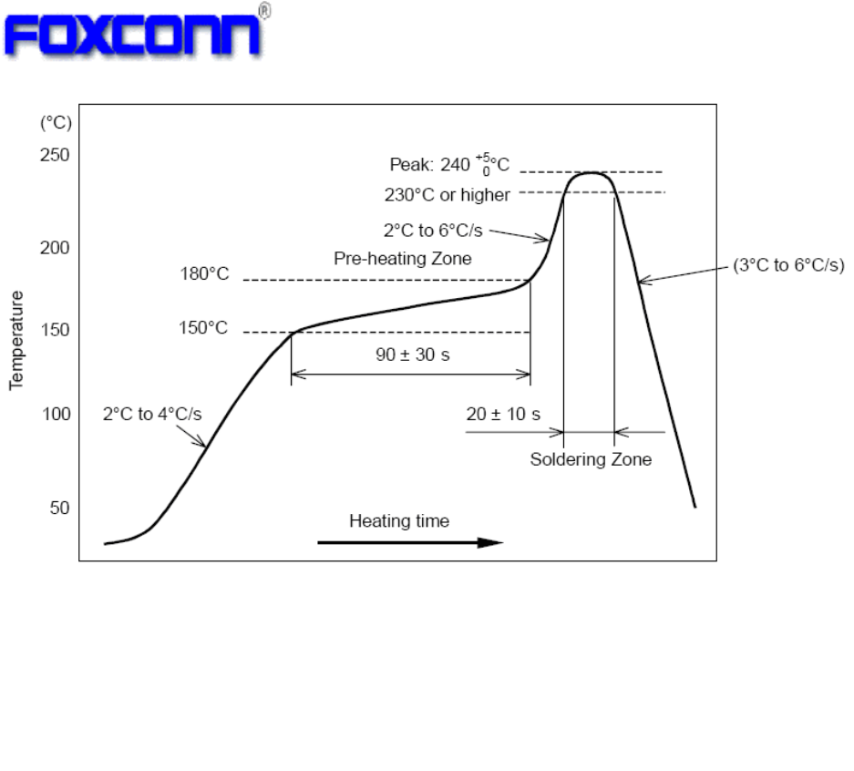
6.6 Soldering and reflow condition
1) Heating method
Conventional Convection or IR/convection
2) Temperature measurement
Thermocouple d=0.1mm ~ 0.2mm CA (K) or CC (T) at soldering portion or equivalent method.
3) Solder paste composition
Sn/3.0Ag/0.5Cu
4) Allowable reflow soldering times: 2 times based on the below reflow soldering profile
5) Temperature profile
Reflow soldering shall be done according to the below temperature profile.
6) Peak temp: 245 degree C
COMPANY CONFIDENTIAL
Temperature profile for evaluation of solder heat resistance of a
component (at solder joint)

COMPANY CONFIDENTIAL
FCC Regulations:
This device complies with part 15 of the FCC Rules. Operation is subject to the following two conditions: (1)
This device may not cause harmful interference, and (2) this device must accept any interference received,
including interference that may cause undesired operation.
This device has been tested and found to comply with the limits for a Class B digital device, pursuant to
Part 15 of the FCC Rules. These limits are designed to provide reasonable protection against harmful
interference in a residential installation. This equipment generates, uses and can radiated radio frequency
energy and, if not installed and used in accordance with the instructions, may cause harmful interference to
radio communications. However, there is no guarantee that interference will not occur in a particular
installation If this equipment does cause harmful interference to radio or television reception, which can be
determined by turning the equipment off and on, the user is encouraged to try to correct the interference by
one or more of the following measures:
-Reorient or relocate the receiving antenna.
-Increase the separation between the equipment and receiver.
-Connect the equipment into an outlet on a circuit different from that to which the receiver is connected.
-Consult the dealer or an experienced radio/TV technician for help.
Changes or modifications not expressly approved by the party responsible for compliance could void the
user‘s authority to operate the equipment.
Operation on the 5.15-5.25GHz frequency band is restricted to indoor use only.
The device marketed to the US/Canada is firmware limited to operate only on channel 1~11.
RF Exposure Information
This Modular Approval is limited to OEM installation for mobile and fixed applications only. The antenna
installation and operating configurations of this transmitter, including any applicable source-based
time-averaging duty factor, antenna gain and cable loss must satisfy MPE categorical Exclusion
Requirements of §2.1091.
The antenna(s) used for this transmitter must be installed to provide a separation distance of at least 20 cm
from all persons, must not be collocated or operating in conjunction with any other antenna or transmitter,
except in accordance with FCC multi-transmitter product procedures.
The end user has no manual instructions to remove or install the device and a separate approval is required
for all other operating configurations, including portable configurations with respect to 2.1093 and different
antenna configurations.
Maximum antenna gain allowed for use with this device is 2.5 dBi for 2.4GHz, 2.48dBi for 5GHz.
When the module is installed in the host device, the FCC ID label must be visible through a window on the
final device or it must be visible when an access panel, door or cover is easily re-moved. If not, a second
label must be placed on the outside of the final device that contains the following text: “Contains FCC ID:
HLZ-T77H389”.

COMPANY CONFIDENTIAL
IC Regulations:
This device complies with Industry Canada license-exempt RSS standard(s). Operation is subject to the
following two conditions:
(1) this device may not cause interference, and
(2) this device must accept any interference, including interference that may cause undesired operation of
the device.
Le présent appareil est conforme aux CNR d'Industrie Canada applicables aux appareils radio exempts de
licence. L'exploitation est autorisée aux deux conditions suivantes:
(1) l'appareil ne doit pas produire de brouillage, et
(2) l'utilisateur de l'appareil doit accepter tout brouillage radioélectrique subi, même si le brouillage est
susceptible d'en compromettre le fonctionnement."
This Class B digital apparatus complies with Canadian ICES-003.
Cet appareil numérique de la classe B est conforme à la norme NMB-003 du Canada.
To reduce potential radio interference to other users, the antenna type and its gain should be so chosen that
the equivalent isotropically radiated power (EIRP) is not more than that required for successful
communication. This device has been designed to operate with an antenna having a maximum gain of 2.5
dBi for 2.4GHz, 2.48dBi for 5GHz.. When the module is installed in the host device, the IC label must be
visible through a window on the final device or it must be visible when an access panel, door or cover is
easily re-moved. If not, a second label must be placed on the outside of the final device that contains the
following text: “Contains IC: 1754F-T77H389”.
Antenna having a higher gain is strictly prohibited per regulations of Industry Canada. The required antenna
impedance is 50 ohms.
To reduce potential radio interference to other users, the antenna type and its gain should be so chosen that
the equivalent isotropically radiated power (e.i.r.p.) is not more than that permitted for successful
communication.
This device and its antenna(s) must not be co-located or operating in conjunction with any other antenna or
transmitter.
The County Code Selection feature is disabled for products marketed in the US/Canada
The device for the band 5150-5250 MHz is only for indoor usage to reduce potential for harmful interference
to co-channel mobile satellite systems; the maximum antenna gain permitted (for devices in the bands
5250-5350 MHz and 5470-5725 MHz) to comply with the e.i.r.p. limit; and The maximum antenna gain
permitted (for devices in the band 5725-5850 MHz) to comply with the e.i.r.p. limits specified for point-to-point
and non point-to-point operation as appropriate, as stated in section A9.2(3). In addition, High-power radars
are allocated as primary users (meaning they have priority) of the band 5250-5350 MHz and this radar could
cause interference and/or damage to LE-LAN devices.
IMPORTANT NOTE:
IC Radiation Exposure Statement:
This equipment complies with IC RSS-102 radiation exposure limits set forth for an uncontrolled environment.
This equipment should be installed and operated with minimum distance 20cm between the radiator & your
body.

COMPANY CONFIDENTIAL
R&TTE Regulation:
In all cases assessment of the final product must be mass against the Essential requirements of the
R&TTE Directive Articles 3.1(a) and (b), safety and EMC respectively, as well as any relevant
Article 3.3 requirements.
The maximum antenna gain is 2.5 dBi for 2.4GHz, 2.48dBi for 5GHz. and the antenna separation
distance is 20cm.
The maximum ambient temperature for operating will not be higher than 70 ˚C.
This equipment may be operated in:
AT
BE
BG
CH
CY
CZ
DE
DK
EE
ES
FI
FR
GB
GR
HU
IE
IT
IS
LI
LT
LU
LV
MT
NL
NO
PL
PT
RO
SE
SI
SK
TR