Actiontec Electronics RGM840 RGMII 802.11ac WLAN module User Manual UserMan
Actiontec Electronics Inc RGMII 802.11ac WLAN module UserMan
Contents
- 1. UserMan (statement)
- 2. UserMan
UserMan
Actiontec 11ac RGMII Module User’s Guide
Part Number: RGM840
Revision 1.3
Date: 10/21/2013
Subject to change
1. Introduction
This document provides the hardware specification for RGM840 module. This module supports
802.11ac standard with 5GHz 4x4 MIMO, 4 spatial streams, transmit beamforming and etc. This
11ac RGMII module uses local memory and flash to fully offload the host processor on the main
board so only minimal software is required on the host for management purpose.
2. Block diagram
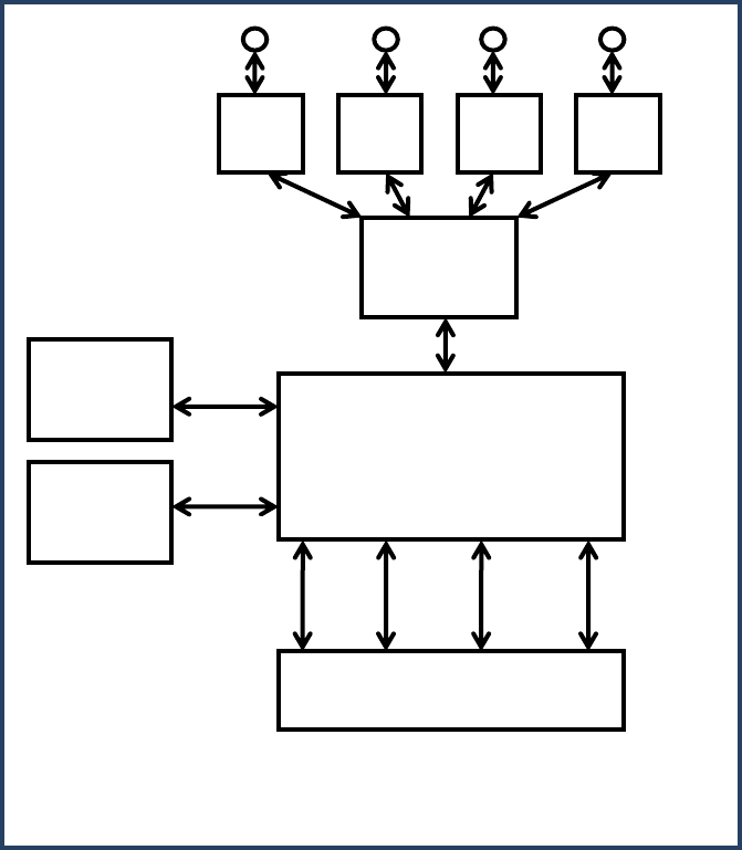
The block diagram of the module is shown in figure 1. As indicated in the diagram, this module
uses a proprietary RGMII over mPCIe interface and provides 4 U.FL antenna connectors for
cable antenna.
Figure 1. Block Diagram of the RGM840 module
RGMII over mPCIe
RGMII over mPCIe
I/F
DDR3
WPS
Input
WPS
Input
RGMI
I
RGMI
I
UART
UART
LEDs/
GPIOs/
HRST
LEDs/
GPIOs/
HRST
QT3840BC
QT2518B
FEM
FFE
M
FEM
FFE
M
FEM
FFE
M
FEM
FFE
M
U.FL
U.FL
64KB
Flash
SPI0

3. General feature list
Feature list
Descriptions
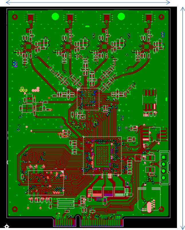
Target dimensions [mm]
80mm(L) x 60mm(W)
Signaling connection
RGMII connection over mPCIe connector
Antenna connection
4 antenna connections via U.FL connectors .
PCB
6 Layers
Chipset
QV840 (QT3840BC and QT2518B)
RF FEM
Microsemi LX5586H or Triquint TQP8080 (subject to change)
Band support
5GHz
Freq support
5180-5825MHz
BW
20MHz/40MHz/80MHz Mixed mode
Spatial Streams
Up to 4SS
Configuration and System
management
In-band or Web GUI
WPS
WPS input pin
Wi-Fi LED
Wi-Fi LED signal pin
WPS LED
WPS LED signal pin
Radio ON/OFF Control
Radio enable/disable pin
Factory reset
Factory reset to default input via mPCIe connector
Hard reset
Hardware reset input via mPCIe connector
UART
via mPCIe connector
DDR3 Memory
16bit – 128MB, 400MHz
SPI flash
64KB ( firmware downloaded via RGMII interface ) or 16MB
Calibration data storage
SPI flash
Power Source
via mPCIe connector, 3.3V-2.5A and optional 5V for FEM
Interoperability
Operates with 802.11a/n/ac clients/STA and AP
MIMO features
MU-MIMO, Tx Beamforming and LDPC
Security
WPA,WPA2
4. RF Specification
Items
Target Specification
Total max conductive output
power
24dBm with 3.3V
TX EVM at antenna port (Subject
to change for manufacturing)
+17dBm @3% EVM, HT40, MCS7
+15dBm @1.8% EVM , MCS9 (subject to change)
RX min. sensitivity (Subject to
change for manufacturing)
20MHz MCS0 -93dBm
20MHz MCS7 -75dBm
40MHz MCS0 -90dBm
40MHz MSC7 -72dBm

80MHz MCS0 -87dBm
80MHz MCS7 -66dBm
80MHz MCS9 -60dBm
Output power accuracy
+/- 1.5 dB max
5. Pin assignment
Pins
Definitions
Pin Type
Pins
Definitions
Pin Type
1
5V
5V DC Input
2
5V
5V DC Input
3
5V
5V DC Input
4
5V
5V DC Input
5
GND
Ground
6
GND
Ground
7
EXTRST
Reset Output
8
AGPIO_B_10
Bidirectional
9
GND
Ground
10
AGPIO_B_11
Bidirectional
11
GMDIO_B
Bidirectional
12
GMDC_O
Output
13
GRXD_I_3
Input
14
WLAN_DISABLE
(AGPIO_B_12)
Input (0 : Disable)
15
GRXD_I_1
Input
16
GRXD_I_2
Input
17
GRXCLK_I
Input
18
GRXD_I_0
Input
19
GND
Ground
20
RXDV_I
Input
21
GTXCLK_O
Output
22
GND
Ground
23
GND
Ground
24
GTXCLK_I
Input
25
GTXEN_O
Output
26
GND
Ground
27
GTXD_O_3
Output
28
GTXD_O_1
Output
29
GTXD_O_2
Output
30
GTXD_O_0
Output
31
GND
Ground
32
RTD (Reset to
Default)
(AGPIO_B_5)
Input
33
25M_GPHY
Output
34
AGPIO_B_16
Bidirectional, PWM
35
GND
Ground
36
AGPIO_B_6
Output
37
1_AGPIO_B_8
Output (UART TX)
38
WPS_LED2
(AGPIO_B_13)
Output, PWM
39
WLAN_LED
(AGPIO_B_1)
Output, 3.3V,
PWM
40
1_AGPIO_B_0
Input (UART RX)
41
WPS
(AGPIO_B_4)
Input (0: Active)
42
GND
Ground
43
WPS_LED1
(AGPIO_B_3)
Output, 3.3V,
PWM
44
HRST
Input (0 : Active)
45
GND
Ground
46
GND
Ground
47
3.3V
3.3V DC Input
48
3.3V
3.3V DC Input
49
3.3V
3.3V DC Input
50
3.3V
3.3V DC Input
51
3.3V
3.3V DC Input
52
3.3V
3.3V DC Input

6. Module power requirement
Power supply: 3.3V DC input
Max output power per chain = 18dBm (LX5586H or TQP8080)
Voltage rails
RMS Current rating (Max)
3.3V only
2.5A
7. Hardware reset (HRST) requirement
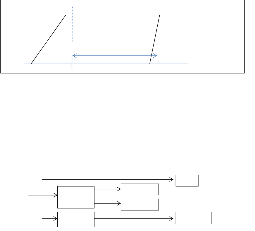
Since the HRST signal is connected to the hard reset of QT3840BC and is also used to start the linux boot
via RGMII interface, therefore it should be connected to the GPIO pin of the network processor so that it
can be controlled by software. Once the HRST signal is deasserted, the module will start to request tftp
server running on the host processor to fetch the bootloader and firmware image. The HRST should be
keep low for no less than 30ms after the 3.3V supply reaches the nominal voltage.
8. Power Management Unit (PMU)
The power management unit is a new feature integrated into the QT3840 chip and it consists of 3
switching regulators and 3 LDOs. The 3 buck converters are designed specifically to generate 1.1V for
QT3840 core voltage, 1.2V for QT2518B, 1.5V for DDR3. The LDOs provide clean output voltages for
oscillator, RF synthesizer and AFE block. In the latest revision of QTM840 RGMII module design, 1.1V for
QT3840 core voltage is fed by external DC-DC switching regulator instead of PMU in the purpose of
reducing the heat dissipation inside the QT3840 package.
3.3V
HRST
3.3V IN
30ms
QT3840BC
PMU
FEM
3.3V IN
DC-DC SW
1.1V Core
1.2V RFIC4
1.5V DDR3
9. Mechanical drawing
10. Compliance Certifications
1. FCC EMI Certification – pending
2. FCC DFS Certification – pending
3. WiFi Certification - pending
60mm
80mm

11. RGMII interface connection example
RGMII signals from the host processor
RGMII signals from RGMII module pin assignments
Signals
Pin descriptions
Pin Type
Pin
Signals
Pin Type
GTXD3
RGMII Transmit data bit 3
Output
13
GRXD_I_3
Input
GTXD2
RGMII Transmit data bit 2
Output
16
GRXD_I_2
Input
GTXD1
RGMII Transmit data bit 1
Output
15
GRXD_I_1
Input
GTXD0
RGMII Transmit data bit 0
Output
18
GRXD_I_0
Input
GTXEN
RGMII Transmit enable
Output
20
RXDV_I
Input
GTXCLK
RGMII 125MHz TXCLK
Output
17
GRXCLK_I
Input
GRXCLK
RGMII receive clock
Input
21
GTXCLK_O
Output
1K Pull down resistor
24
GTXCLK_I
Input
GRXDV
RGMII receive data valid
Input
25
GTXEN_O
Output
GRXD3
RGMII Receive data bit 3
Output
27
GTXD_O_3
Output
GRXD2
RGMII Receive data bit 2
Output
29
GTXD_O_2
Output
GRXD1
RGMII Receive data bit 1
Output
28
GTXD_O_1
Output
GRXD0
RGMII Recevie data bit 0
Output
30
GTXD_O_0
Output
1k Pull down resistor
33
25M_GPHY
Output
12. MDIO/MDC
QT3840BC has a MDIO master controller so it can be used to manage any MDIO slave device on the host
board. The two signals are provided on pin 11 and pin 12 of the mPCIe connector. If there is no need for
QT3840BC to be the MDIO master, then pull down both MDC and MDIO signal to ground with 1K ohm
resistor.
13. 25M_GPHY
25M_GPHY is a free running 25MHz clock generated by QT3840BC.
14. Booting from 64KB SPI flash
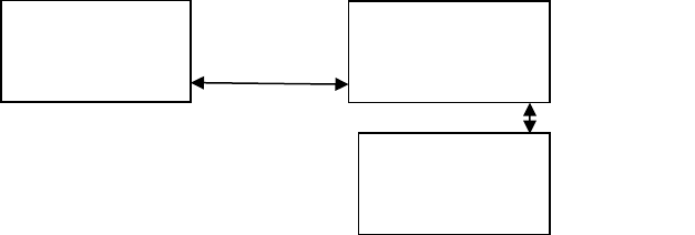
The 64K Byte SPI flash is a cost reduction version of booting from flash mode. The small size of
SPI flash is required to store only the mini-uboot with tftp client feature, calibration data and a
small file system. The external host processor will be required to use its flash memory to store
the uboot and linux image for this module. Besides, it will be allowed to control the boot up
sequence of the target by controlling the hardware reset to the module via pin 44 ~HRST. When
the hardware reset is released, the mini uboot will decompress itself into the internal SRAM of
QT3840BC and then start the tftp client to download the full uboot code and linux image from
external processor via xMII bus to the DDR3 memory of the target. Both target and external
host will need IP addresses for the tftp procotol to work. After the linux kernel is boot up, the
system looks the same as booting from the big flash mode.
Note: The RF calibration of the QTM840 chipset is required for on each target board and it is
executed internally but requires the external calibration software to control DUT and the
Litepoint equipment via telnet session. For any system with external host processor, ethernet
bridge between external ethernet port to wifi ethernet port is needed to bridge the RF
calibration control packets to the QT3840BC.
PC: 1.1.1.1
Ethernet
Host:1.1.1.0
QT3840BC:
1.1.1.2
RGMII
15. WPS description
The WPS pairing input pin is assigned to pin 41 on the connector and it is active low input. The WPS
input pin can be connected to on board push button or host processor. The current timing requirement
to trigger WPS function is in low state for no less than 6s but the timing can be adjusted.
16. LED description
There are 3 LEDs provided by the modules and it is active high output signal with pulse width
modulation feature.
1. WLAN_LED (AGPIO_B_1) – Wifi 5GHz LED
Turn on when wifi connection is available
Turn off when wifi connection is not available
Blinking when negotiation or traffic is on line
2. WPS_LED1(AGPIO_B_3) and WPS_LED2 (Red – AGPIO_B_13)
Green on when WPS pairing is active
Blinking 2Hz Green when WPS negotiation is in progress
Solid Red when WPS registration failed
Both off when WPS functionality is disabled
17. Spare GPIO description
There are 3 spare GPIO reserved for future use. They are AGPIO_B_10, AGPIO_B_11, and
AGPIO_B_16. Those spare GPIOs can be connected to host processor for general use. The
default state of all GPIOs is in input state.
AGPIO_B_10 and AGPIO_B_11 are pulled up on the module.
AGPIO_B_16 are floating on the module and please pulled down if not needed on the main
board.
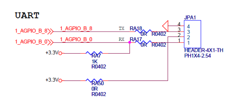
18. Console port (UART)
The console port of the module is provided on the module and also through pin 37 (1_AGPIO_B_8) and
pin 40 (1_AGPIO_B_0) of the mPCIe interface. Host processor can communicate to the module through
the console port.
1_AGPIO_B_8 – UART TX signal
1_AGPIO_B_0 – UART RX signal (1K pull up resistor is required at pin 40 of mPCIe connector on the host
processor board)
19. EMI and Antenna isolation requirement
This module is a 5GHz only radio and requires 25dB isolation from 2.4GHz antenna when dual band dual
concurrent mode is supported in the final product. Otherwise, the throughput performance will be
degraded due to harmonics of 2.4GHz leaking into the 5GHz radio band.
The SoC motherboard typically consists of many subsystems such as DDR2, DDR3, A/VDSL, VOIP, USB
and other high speed interfaces. Each subsystem will operate on different clock frequencies and its
harmonics could fall into the 5GHz band. Please make sure the EMI radiated from different clocks on the
board can be contained or mitigated by either HW or SW solution.