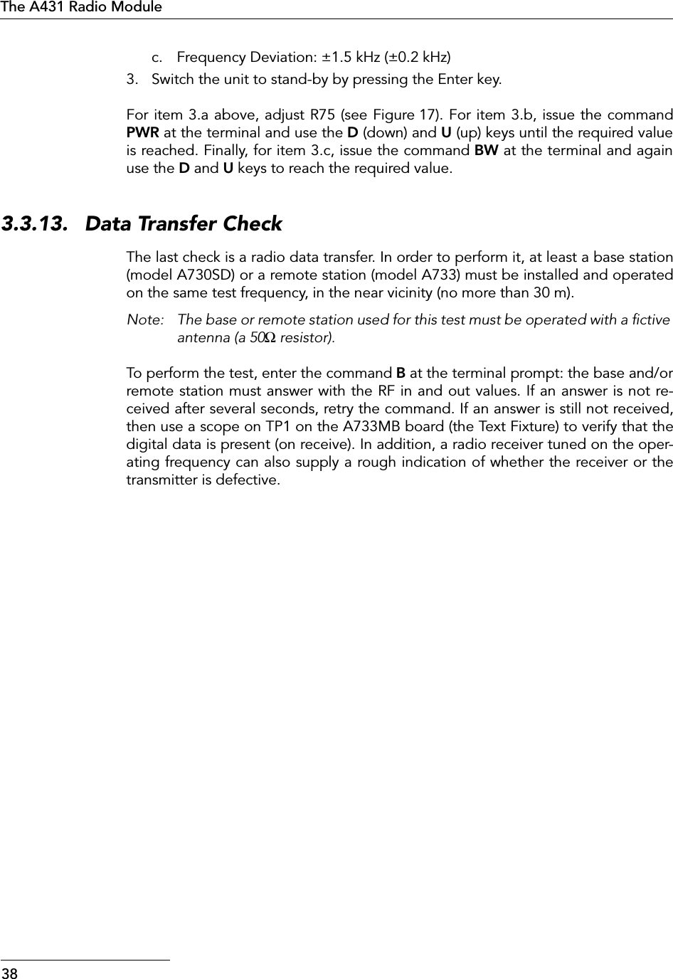
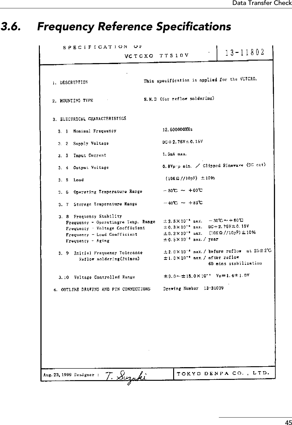
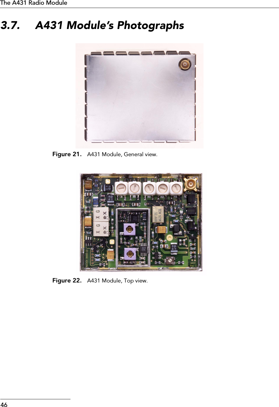
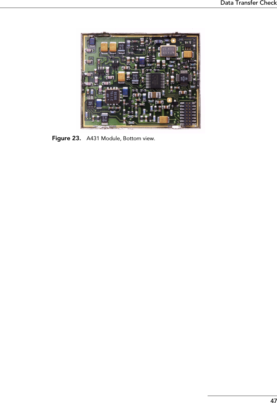
Adcon Telemetry A440 Wireless Telemetry Modem User Manual A440 Technical Reference

Adcon Telemetry Inc Wireless Telemetry Modem A440 Technical Reference

users manual revised

 ADCONTELEMETRY SMART WIRELESS SOLUTIONS A440 Wireless Modem Technical Reference Manual
  ADCONTELEMETRYADCON TELEMETRY AGINKUSTRASSE 24A-3400 KLOSTERNEUBURGAUSTRIATEL:  +43 (2243) 38 280-0FAX: +43 (2243) 38 280-6http://www.adcon.atADCON TELEMETRY INC1001 YAMATO ROAD SUITE #305, BOCA RATONFL 33431 USATEL: +1 (561) 989-5309FAX: +1 (561) 989-5310http://www.adcon.comADCON TELEMETRY SRLBD. ION IONESCU DELABRAD 8R-71592 BUCHARESTROMANIATEL: +40 (1) 490-6083FAX: +40 (1) 490-6086http://www.adcon.ro Proprietary Notice: The Adcon logo, the A730 series, A720 series and addIT™, A440 and add-WAVE, addVANTAGE® and AgroExpert™ are trademarks or registered trade-marks of Adcon Telemetry AG. All other registered names used throughoutthis publication are trademarks of their respective owners.This publication contains confidential information, property of Adcon Teleme-try AG. Disclosure to third parties of the information contained herein is pro-hibited. Neither the whole nor any part of the information contained in thispublication may be reproduced in any material form except with the prior writ-ten permission of Adcon Telemetry AG.Release 1.0, February, 2001Copyright © 2001 by Adcon Telemetry AG.All rights reserved.
 3 Table of Contents Introduction ____________________________________________________7 About the A440 ______________________________________________________________ 7 Hardware _______________________________________________________9 Overview_____________________________________________________________________ 9 The Modem Interfaces ________________________________________________________________ 10The Microcontroller and the Power Conditioning Sections _________________________________ 10The Power Supply and Serial Interface___________________________________________________ 13External Power Supply_________________________________________________________________ 13 Specifications________________________________________________________________13PCB Parts Placement (A440) __________________________________________________15Bills of Materials _____________________________________________________________15 A440MB _____________________________________________________________________________ 16 A440 Device’s Photographs___________________________________________________21 The A431 Radio Module  _______________________________________ 27 About the A431 Radio Module________________________________________________27Functional description________________________________________________________27 Receiver Section ______________________________________________________________________ 27Transmitter Section____________________________________________________________________ 28 Manufacturing Issues _________________________________________________________30 Marking and labeling issues ____________________________________________________________ 30
 4 Alignment Range and Switching Range __________________________________________________ 30Tuning Procedure _____________________________________________________________________ 31Setting Up the Default Parameters ______________________________________________________ 31Commands valid for all bands ____________________________________________________ 32Commands required for band 1  __________________________________________________ 32Commands required for band 2  __________________________________________________ 32Commands required for band 3  __________________________________________________ 32Commands required for band 4  __________________________________________________ 32Definitions ___________________________________________________________________________ 33Test Equipment Settings _______________________________________________________________ 34Network Analyzer (HP 8712 or equivalent)_____________________________________________ 34Service Monitor (Rohde & Schwarz CMS50 or equivalent) _______________________________ 34Trimming Elements ____________________________________________________________________ 35Adjusting the Receiver Front End _______________________________________________________ 35Adjusting the VCOs ___________________________________________________________________ 36Adjusting the Crystal Reference _________________________________________________________ 37Checking the Receiver Parameters ______________________________________________________ 37Checking the Transmitter Parameters ____________________________________________________ 37Data Transfer Check ___________________________________________________________________ 38 PCB Parts Placement_________________________________________________________ 39Bill of Materials (A431) _______________________________________________________ 41Frequency Reference Specifications ___________________________________________ 45A431 Module’s Photographs _________________________________________________ 46 Software ______________________________________________________49 Short Description____________________________________________________________ 49Tasks _______________________________________________________________________ 49Controlling the Unit__________________________________________________________ 50 Serial Communication Protocol _________________________________________________________ 50General Format of a Command _________________________________________________________ 50General Format of an Answer___________________________________________________________ 51Commands___________________________________________________________________________ 51 CMDS _____________________________________________________ 51TIME _____________________________________________________ 51 SR ____________________________________________________________________________ 52BL ____________________________________________________________________________ 52FREQ _________________________________________________________________________ 53DATA _________________________________________________________________________ 53INFO _________________________________________________________________________ 54RX ____________________________________________________________________________ 55
 5 TX ___________________________________________________________________________ 55B ____________________________________________________________________________ 56Returned errors list____________________________________________________________________ 56Command line interpreter _______________________________________________________ 56Device descriptors and storage handler ___________________________________________ 57Real time clock  ________________________________________________________________ 57Radio interface  ________________________________________________________________ 57Notifications __________________________________________________________________ 57 Adcon Packet Radio Protocol _________________________________________________57 Digital Squelch _______________________________________________________________________ 58Modulation Technique Used (low speed modem) _________________________________________ 59Generic Format of a Radio Frame _______________________________________________________ 59Data Frames _________________________________________________________________________ 61
 6
 7 1. Introduction 1.1. About the A440 The A440 Wireless Modem is a portable low-power, medium-range serial interfacetelemetry modem. The unit is based on a powerful 8-bit Flash RISC microcontroller,which can also be programmed in the field (for software upgrades).The units incorporates an A431 radio module operating in the 430 to 470 MHzrange, making it adaptable to most radio communication regulations in the world.The output power is 0.5 W, while the modulation is narrow band FM (12.5, 20 or 25kHz channel spacing).Due to its construction, as well as to the software controlling it, the power consump-tion is extremely low (average 1 mA). The unit operates from an extrenal 5.6 to 10volt power supply. The power is fed via the common data/power connector/cable.The A440 is a ruggedized unit, complying with the IP65 environmental protectionclass (NEMA 4). It can be easily installed and is compatible with both the standardAdcon low speed protocol and the upcoming high speed protocol.This manual describes the technical details of the A440, both hardware and soft-ware. It is organized in several parts, as follows:• Hardware: includes the schematics as well as a description of the main boardof the A440 (the processor, modems and interfaces)• The A431 radio module: includes the schematics and description of the radiomodule• Software: a short description of the software with the most important com-mands that can be used to control the unit over the serial interface
 8Introduction This manual is intended for the radio approval authorities and laboratories.
 9 2. Hardware 2.1. Overview Most of the electronics (including the A431 radio module) are situated on the mainboard (for the A431 description, see “The A431 Radio Module” on page 27). Themain board (Figure 1) contains the radio unit, a low-speed and a high speed modeminterface, a microcontroller, RS-485 and RS-232 interfaces and a power conditioningsubsystem. The power and the serial lines are provided over a corresponding con-nector (4-pin Binder for RS-485 or D-sub 9 pin for RS-232), while the antenna is fedthrough a 50  Ω  TNC connector. Figure 1. A440 Block Diagram.A431 RadioAntennaµControllerModemInterface PowerConditioningSystem SupplyPower ModuleLow SpeedModemInterfaceHigh SpeedLevelShifterRS485/RS232InterfacesSerial
 10Hardware For further details, consult the schematic diagram in Figure 2. 2.1.1. The Modem Interfaces The low speed modem operates with two tones: 1 kHz (representing the “1” bits)and 2 kHz (representing the “0” bits). A bit cell is represented by a complete timeperiod ( 1/f ), thus the raw throughput varies between 1 and 2 kbps (average 1.5kbps). The modem functions are essentially implemented in software by a separatemicroprocessor. However, a signal pre-conditioning is performed on both receiveand transmit paths by means of two low-pass filters (U6 on receive and U19 on trans-mit).On receive, the buffered analog data signal from the radio unit is applied to a 3 kHzlow pass filter (U6). The filter output is further fed to the A/D input of a slave micro-controller U5) performing the decoding operation for the low speed modulation(see also “Modulation Technique Used (low speed modem)” on page 59). The slavemicrocontroller (U5) communicates with the main microcontroller (U9) via a 4-wire in-terface. In addition, the audio output from the radio unit is also applied to the GMSKmodem (U7) for decoding high speed data.On transmit, the low speed data is generated again by the slave microcontroller (U5)added by the R/2R network implementing a D/A converter. The slave microcontrol-ler generates in effect the sinus waveforms required to encode the binary data. Theoutput signal is applied to the audio mixer U11, which adds the signal generated bythe high speed modem (U7). Obviously, only one modem will be activated at a timeby the master microcontroller (U9). The output signal of the mixer is applied to thevariable gain amplifier (U15) and then to the final low pass-filter (U19) that has a cut-off frequency of around 7 kHz.The high speed modem (U7) has two clocking options: either it can be clocked fromthe main microcontroller’s clock via a buffer (U20), or it can be driven by its ownquartz crystal (X3). The low speed modem (U5) is always driven by the main micro-controller’s clock. 2.1.2. The Microcontroller and the Power Conditioning Sections The operation of the whole unit is under the control of U9, an Atmel ATMega 103microcontroller. It is a powerful chip exhibiting a very low power consumption. Itsmain functions are:• Controls the radio unit• Control the modems functionality• Assembles the radio frames and waits for requests from a remote• Implements Adcon radio and RS-485 protocol stack• Manages the real-time clock
 11The Microcontroller and the Power Conditioning Sections • Implements a serial Command Line Interface (CLI)The chip operates at its maximum speed, in this case 4 MHz (the “L” version), anduses a crystal (X2) for the on-board clock generator. The real time clock is imple-mented by means of a 32.768 kHz crystal (X1) connected on the internal Timer/Counter0.The radio unit is controlled via the SPI bus (to set the PLL chip parameters) and viaseveral ports of the microcontroller for such operations as transmit and receive. Inaddition, the high current 5 volt LDO voltage source (U4) is switched on before theradio module’s PA is activated. The power output is adjusted by means of an elec-tronic potentiometer (U2).The A/D subsystem is used to sample the RSSI and Pout inputs. A stable 2.5 Voltreference supplied by U3 is applied to the A ref  pin. The reference is powered by themicrocontroller only when sampling the A/D input.The serial interface is implemented by means of the built-in UART. Both the RS-232and RS-485 interfaces are implemented using Maxim chips (U12 and U17 respective-ly). The serial interface mode is selected by means of a pair of jumpers (J1).An additional amount of 32Kbytes RAM is provided to the main microcontroller; theRAM chip (U8) is attached to the multiplexed bus of the microcontroller with the aidof a latch (U10). A brown-out supervisor chip (U14) is used to assure a smooth start-up of the micro-controller and avoid possible erratic behavior when the supply level descends belowthe minimum operating value (2.7 volts).A LDO voltage regulator (U16) is used to provide 3.3 Volt power to the main com-ponents on the board.
 13The Power Supply and Serial Interface 2.1.3. The Power Supply and Serial Interface The interface connector allows for:• External supply (any DC source from 5.6 to 10volts)• Communication over serial lines, at 19200 baud(RS-485).For testing purposes, Adcon supplies a 220VAC poweradapter that provides also an RS-485 to RS-232 conversion. Thus, the unit can beconnected to a serial port of a PC and can be switched in various operating modes.A list of commands is given in the sub chapter “Controlling the Unit” on page 50. 2.1.4. External Power Supply In order to test the unit over the specified supply range, a special power cable is sup-plied by Adcon Telemetry. This cable must be connected to the interface connectorof the unit  before  the serial cable (see Figure 3). The two wires with banana plugsmay then be connected to an external variable power supply: the red plug to plusand the black plug to minus.  WARNING!  Do not apply more than 10 Volts to the unit: permanent damage of thedevice may result. Figure 3. Connection of an external power supply. 2.2. Specifications The A440 fulfills the specifications of the EN 300 220-1, Class 12, and ETS 300 113,as well as the FCC Part 90.214 (Subpart J) of the CFR 47.1234V+BAGndINTERF+-BlackRed5.6 to 10 VoltANT To Interface UnitA440
 14Hardware Note: The parameters below were measured with the A440 + A431 combination. Parameter Min. Typ. Max. Unit CommonSupply 5.6 6.2 10.0 VOperating Temperature -30 +70 °CRelative Humidity 99 %Class Protection IP65RF Data Rate (Using the low-speed Modem) 1000 1500 a a. Data rate is content dependent. 2000 bpsRF Data Rate (Using the high-speed Modem) 8000 bpsOperating Frequency (-44 version) b b. This parameter represents the alignment range; the switching range canbe limited in software to a narrower space (even to the extent of a singlechannel). 430 450 MHzOperating Frequency (-46 version) b 450 470 MHzFrequency Stability (-20 to +50°C) ±1.5 kHzFrequency Stability (-30 to +60°C) ±2.5 kHzReceive modeSensitivity (12 db S/S+N) -118 dBmImage Frequency Attenuation (1st IF = 45 MHz) -70 dBLocal Oscillator Leakage 2 nWAdjacent Channel Attenuation (12.5 kHz mode) -57 dBRSSI dynamic 90 dBOperating Current (incl. On-board Microcontroller) 32 mATransmit mode (all measurements made on a 50  Ω  resistive load)Output Power 27 dBmSpurious Radiation 200 nWAdjacent Channel Power (12.5 kHz mode) -34 dBmOccupied Bandwidth (12.5 kHz mode) 7.0 kHzOperating Current (incl. On-board Microcontroller) 600 mA
 21A440MB 2.5. A440 Device’s Photographs Figure 6. A440, Front view. 55 1 XTAL-MC306 32.76KHzMC-306 X1 Seiko Epson56 SMD Header 1 SLY8/SMD/055/4 S 2mm J1 Fischer Elektronik57 Jumper 1 CAB10 2mm to J1 Fischer Elektronik Pos Description Count Component Name Value Pattern Ref Des Manufacturer
 22Hardware Figure 7. A440, Back view.
 23A440MB Figure 8. A440, Top view. Figure 9. A440, Bottom view.
 24Hardware Figure 10. A440, Left and Right views.
 25A440MB Figure 11. A440, Case opened. Figure 12. A440 Motherboard, top view.
 26Hardware Figure 13. A440 Motherboard, bottom view.
 27 3. The A431 Radio Module 3.1. About the A431 Radio Module The A431 was specially designed for narrow-band FM data communication. It exhib-its a relatively flat response in the audio band from 10 Hz to 2.5 kHz, both on sendas well as on receive paths. Additionally, the receiver’s group delay is very low.The module operates in the 430 to 470 MHz range, making it compatible with mostradio communication regulations in the world. The output power is 0.5 W, while themodulation is narrow-band FM (12.5, 20 or 25 kHz channel spacing). The power con-sumption in receive mode is remarkably low (under 32 mA), in spite of the good IP3characteristics and high sensitivity. The switching from receive to transmit is fast, un-der 20 mS. 3.2. Functional description The following functional description refers to the schematic diagram in Figure 14. 3.2.1. Receiver Section The antenna signal is fed through the common low-pass filter for both receive andtransmit and applied to the U3 antenna switch. From the J3 port of the switch, it isthen fed to the FL1 helical filter and amplified by the LNA built with Q2 that assuresa high amplification factor (over 20 dB). Another helical filter follows (FL2), giving atotal of more than 70 dB attenuation of the first image frequency.
 28The A431 Radio Module The incoming signal is then applied to the first mixer, U7, through an LC impedancematching network (L12/C48). The local oscillator signal is obtained by means of theVCO built around U10 and applied to the mixer (the LO has a lower frequency thanthe incoming signal). The VCO is locked to the OSC1 reference by means of the U9dual-PLL chip.The mixer’s output on 45 MHz is filtered by means of XF1, which is needed to ensurea sufficient attenuation (over 70dB) of the second image frequency (at 44.090 MHz).The second local oscillator is built around the IF chip, but it is locked by means ofthe second PLL of U9. In this way, all signals are generated from a common referenceoscillator (OSC1, see also “Frequency Reference Specifications” on page 45).The IF chain chip amplifies the signal to a proper level for FM detection. A particu-larity of this chip is that the FM detector is PLL-based, thus no coils or ceramic dis-criminators are needed. Two ceramic filters, CF1 and CF2, ensure the requiredadjacent channel separation. The audio output is delivered on pin 17 and is slightlyamplified through U11 in order to bring it to 1Vpp, and centered on half the supplyvoltage (which is 3.3 volt approximately). The audio signal is fed out of the moduleon the pin  RXDO  of the interface connector. In addition, an RSSI level signal is ob-tained on pin 18 of U8 and is fed to switch U6. As long as the module is in receivemode, the RSSI signal will be present on the  RSSI/PO  pin of the interface connector. 3.2.2. Transmitter Section The carrier is generated directly on the operating frequency by means of the VCObuilt around U2. The signal is locked on the reference OSC1 with the aid of the dualPLL chip based on U9. The chip, a National Semiconductor LMX2332L, was chosenfor its fast locking scheme, low power consumption, and good RF characteristics.The modulation is applied on both the VCO and the reference, in order to attain aflat characteristic in the whole band (10 Hz to 2.5 kHz). Due to the phase differencesbetween the two modulation points, the signal applied on the reference is invertedby means of U4. Meanwhile, U4 is used to center the reference on the channel (usingthe trimpot R75). The PLL low-pass filter (third-order) composed of C66/C67/R69/R59/C64 is calculated around 400 Hz. R64 is used for the FastLock® mechanism.(For further details on the FastLock mechanism, please consult the National Semi-conductor documentation.)The signal is pre-amplified to approximately 0 dBm by Q1 and then it is applied tothe PA built with U1. The output signal is pre-filtered and impedance-matched bymeans of theC21/L10/C22 low-pass filter and then fed to the antenna switch. Beforereaching the antenna output, a three-cell, low-pass filter (used also on the receivepath) is used to attenuate the unwanted harmonics and keep them below the re-quired limits.
 30The A431 Radio Module An Automatic Level Control (ALC) system is responsible for keeping the output pow-er constant, regardless of the external influences (temperature, VCO excitation and/or supply). A small part of the RF energy is rectified by D2 and applied to the U5:Aamplifier. By means of U5:B, the power is controlled according to the pre-set powerlevel (ALC input). U5:A is basically an analog comparator between the actual and theprogrammed power output. Depending on the error signal obtained, a variable volt-age is applied on the PD input of the PA chip, thus effectively controlling its outputpower. In addition, the actual power output level is fed to the U6 analog switch andpresented to the RSSI/PO output while the unit is switched in transmit mode.The modulation is applied on two-points: the VCO and the reference oscillator—thisis needed to obtain a flat response in the audio range from 10Hz to 2.5 kHz and com-pensate for the counter-effect opposed by the synthesizer loop. The input signal(must be 1 Vpp) is fed through a resistive divider (R14/R13) to the “cold” end of thevaractor diode controlling the VCO (D1). At the same time, the same modulationsignal is applied to the inverting op-amp U4 and then to the OSC1 reference oscil-lator (a VCTCXO). The modulation signal is inverted in order to bring it in phase withthe VCO modulation point. 3.3. Manufacturing Issues 3.3.1. Marking and labeling issues The A431 Module is manufactured in two versions:• Low band—able to operate between 430 and 450 MHz• High band—able to operate between 450 and 470 MHzFrom a manufacturing perspective, the difference between the high and low bandare the two helical filters FL1 and FL2 used on the receiving chain. The low band ver-sion is marked as A440-44 while the high band is marked as A440-46 (when themodules are included into the A440 Wireless Modem). 3.3.2. Alignment Range and Switching Range The A431 radio module’s alignment range is 20 MHz, while the switching range is10 MHz. According to the definitions formulated in the ETS 300220 and ETS 300013specifications, the A431 radio module (combined with the A440 Wireless Modem)belongs to the AR1 category. Therefore, for the European testing, two units shouldbe presented for test purposes, as follows:• One A440 unit containing an A431-44 radio module, alignment range 430-450 MHz, switching range 433-443 MHz• One A440 unit containing an A431-46 radio module, alignment range 450-470 MHz, switching range 455-465 MHz.
 31Tuning Procedure Consequently, two test reports will be provided to Adcon Telemetry AG.For North America (FCC), only the portion 460 to 470 MHz will be used; therefore,a single device model A440-46 having the switching range between 460 and 470MHz will be submitted for testing.3.3.3. Tuning ProcedureThe A431 modules are to be tuned by mounting them on a test fixture consisting ofa specially modified A733 motherboard (the A733 is an universal low cost RemoteTelemetry Unit manufactured by Adcon). The modification refers to certain mechan-ical aspects, in order to provide an easy plug in and out of the control connector (P2)as well as to the TP1 and TP2 test points.The alignment operation must differentiate between following classes of units:• Band 1: from 430 to 440 MHz• Band 2: from 440 to 450 MHz• Band 3: from 450 to 460 MHz• Band 4: from 460 to 470 MHzNote: The boards differ only through the FL1 and FL2, in that Band 1 and 2 use models TOKO 493S-1071A and 492S-1056A while Band 3 and 4 use models TOKO 493S-1075A and 492S-1060A, respectively. In addition, the tuning pro-cedure and some software parameters differ. The differences are clearly stat-ed in the following paragraphs, where applicable.Note: Special versions could also be delivered having switching ranges in-between those defined above; however, it may never exceed 10 MHz.3.3.4. Setting Up the Default ParametersThe tuning procedure is not possible without first configuring some default param-eters for the A733 motherboard used in the testing fixture. This is done via the serialinterface of the motherboard by using a communication terminal program (e.g. Hy-perterminal, in Microsoft® Windows™ 95). The terminal program must be config-ured as follows:• 19200 Baud• 1 Stop bit• No parity• No protocol (neither hardware, nor software)To check if the communication is operational, press theENTER key. Annnnn 0 RxDTxDGroundBatteryExt Power12345
32The A431 Radio Module# prompt should appear on the terminal screen (nnnn is the actual ID of the unit thatis printed on its label). The following default parameters must be pre-loaded (formore information about the meaning of the commands, consult the section “Com-mands” on page 51):Commands valid for all bandsID 1PMP 65 72SLOT 900 15RSSI 58Commands required for band 1SR 430000000 440000000BL 430000000 440000000FREQ 435000000 12500Commands required for band 2SR 440000000 450000000BL 440000000 450000000FREQ 445000000 12500Commands required for band 3SR 450000000 460000000BL 450000000 460000000FREQ 455000000 12500Commands required for band 4SR 460000000 470000000BL 460000000 470000000FREQ 465000000 12500Note: The SR command sets the switching range limits, the BL command sets the band limits, and the FREQ command sets the actual operating frequency; before shipping and depending on the target country, these parameters may be changed. The SL command must be always issued before the BL com-mand and the BL command must always be issued before the FREQ com-mand.
33Definitions3.3.5. DefinitionsThe diagram of the setup environment is depicted in Figure 15.Figure 15. Trimming Setup.The testing fixture is used to fasten the A431 Module under test both mechanicallyand electrically in such a way as to allow its rapid and comfortable alignment. It con-sists of a mechanical board with two screws that are used to fasten the board; twoelastic pins are used to transport the relevant signals from the module to their cor-responding test cables. The directional coupler connects the antenna input/outputof the device under test to both the network analyzer and the service monitor. Theschematic diagram of the testing fixture is depicted in Figure 16.Figure 16. Schematic Diagram of the Testing Fixture.0.765 VOutScope Ant I/O OutVoltmeter OutNetworkAnalyzerTestingFixtureRS232 To/From PC+–6.5 VA733MBConnectorOptionalScope Service Monitor Network Analyzer VoltmeterDirectional CouplerScopeOut NetworkAnalyzerAntGndTP1A733MBTP2TP2 Voltmeter470KΩAntennaA431Module
34The A431 Radio Module3.3.6. Test Equipment SettingsBefore proceeding, certain controls on the test equipment must be set; some of thesettings depend of the operating band (high or low) of the device under test (DUT).In addition, it is highly recommended that the ambient temperature during align-ment is kept to 22° C (±1°C).3.3.6.1. Network Analyzer (HP 8712 or equivalent)The settings for the Network Analyzer are as follows:• Center frequency: 450 MHz• Span: 100 MHz• Display: 10.0 dB/div• Power: -20 dBm• Markers: — band 1: Mkr1 – 435 MHz, Mkr2 – 430 MHz, Mkr3 – 440 MHz— band 2: Mkr1 – 445 MHz, Mkr2 – 440 MHz, Mkr3 – 450 MHz— band 3: Mkr1 – 455 MHz, Mkr2 – 450 MHz, Mkr3 – 460 MHz— band 4: Mkr1 – 465 MHz, Mkr2 – 460 MHz, Mkr3 – 470 MHzNote: It is a good idea to store the instrument state for the four settings for a rapid recall when needed.3.3.6.2. Service Monitor (Rohde & Schwarz CMS50 or equivalent)The setting for the receiver section check are as follows (RX-TEST):• SET RF: 435000000 Hz (Band 1) / 445000000 Hz (Band 2) / 455000000 Hz(Band 3) / 465000000 Hz (Band 4)• RF LEV: -118dBm• SINAD• AF1: 1kHz• MOD1: 2.5 kHz• SCOPE MODE• BEST RANGEThe settings for the transmitter section check (TX-TEST):• COUNT: (should show the transmitter carrier frequency)• POWER: (should show the transmitter carrier power)
35Trimming Elements3.3.7. Trimming ElementsThe location of the trimming elements on the A431 Module is shown in Figure 17.Figure 17. Location of the trimming elements.3.3.8. Adjusting the Receiver Front End1. Mount the DUT (Device Under Test) on the testing fixture and connect it to the host via the serial cable.2. Select the appropriate instrument profile depending on the device’s band.3. Turn the DUT in permanent receive mode by entering the RX command at the terminal.4. Adjust the FL1 and FL2 filters (see Figure 17) until you obtain a curve similar to the one shown in Figure 18 (depending on the band, the markers may be different); this is done by successively adjusting the five trimming screws located on the filters.R75 (Crystal Reference)FL1FL2L15 (RX VCO)L7 (TX VCO)
36The A431 Radio ModuleIf the adjustments do not achieve the appropriate curve, check the power supply,the cable connections to/from the test equipment, etc. Verify also that all the pins ofthe FL1 and FL2 filters are properly soldered.Figure 18. Helical Filter + LNA’s selectivity diagram.3.3.9. Adjusting the VCOs1. Verify that the DUT is in receive mode (enter the RX command at the terminal program).2. Adjust the coil L15 (see Figure 17) until the voltage shown on the digital voltmeter is 1400 mV, ±50 mV (see also the note below).3. Switch the unit to transmit mode by entering TX at the terminal.4. Adjust the coil L7 (see Figure 17) until the voltage shown on the voltmeter is again 1400 mV, ±50 mV.5. Press the enter key at the terminal to switch the unit off.Note: A one-time calibration of the Testing Fixture may be needed due to the in-ternal resistance of the voltmeter and the serial resistor mounted on the Test-ing Fixture. The calibration is performed by measuring the VCO voltage directly on the TP2 and by comparing the value with that measured through the Testing Fixture. The values given above are the real ones, measured di-rectly.If the above limits cannot be obtained, or the readout is unstable, verify the follow-ing:• The programmed operating frequencies are indeed 435 (Band 1), 445(Band 2), 455 (Band 3) and 465 MHz (Band 4). To check this, type the com-mand FREQ at the terminal prompt; the device will answer by returning thecurrent frequency.• The respective commands (RX and TX) were issued.
37Adjusting the Crystal Reference• No parts are missing, or have the incorrect value, or are badly soldered (checkthe parts around U2 and U10).3.3.10. Adjusting the Crystal Reference1. Switch the unit to transmit mode by entering TX at the terminal.2. Observe the indication shown by the Service Monitor: adjust R75 (see Figure 17) until the carrier frequency indicates 435000000 (Band 1), 445000000 (Band 2), 455000000 (Band 3), or 465000000 MHz (Band 4) ± 200 Hz, respectively.3.3.11. Checking the Receiver Parameters1. Switch the DUT to receive mode by entering RX at the terminal.2. Switch the Service Monitor to RX TEST mode, on the appropriate frequency (435 / 445 / 455 or 465 MHz respectively); the level should be -118dBm (see also “Test Equipment Settings” on page 34).3. Verify that the S/N ratio is at least 12 dB; in addition, if a scope is also connected, a clear 1 kHz sine wave should be visible, with a relatively low amount of noise superimposed.4. Switch the DUT to pulsed mode by pressing the Enter key. After several seconds, you will see the image on the scope pulsing at about one-second intervals.5. Switch the RF generator output off.6. Verify that the RSSI threshold is correct by typing the command RSSI; the actual value must be lower than the threshold set. If this is not the case, repeat the RSSI command several times—perhaps the frequency is in use (a radio receiver set on the operating frequency would help detect foreign transmissions). If the threshold difference is marginal, it must be increased by using the RSSI <value> command (it must be 20 to 30% higher than the actual value).If any of the above targets are not reachable, visually verify first that the U8 chip iscorrectly soldered and that there are no shorts between its pins (most problems usu-ally appear around this chip).3.3.12. Checking the Transmitter Parameters1. Switch the DUT to transmit mode by typing the command TX 0 at the terminal.2. Switch the Service Monitor to TX TEST mode, on the appropriate frequency (435 / 445 / 455 or 465 MHz respectively). You should see the following parameters on the Service Monitor readout:a. Carrier: 435000000 ± 200 Hz (or 445000000 / 455000000 / 465000000 respectively)b. Output Power: 26.5 dBm (+ 0.5 dBm / - 1 dBm)
38The A431 Radio Modulec. Frequency Deviation: ±1.5 kHz (±0.2 kHz)3. Switch the unit to stand-by by pressing the Enter key.For item 3.a above, adjust R75 (see Figure 17). For item 3.b, issue the commandPWR at the terminal and use the D (down) and U (up) keys until the required valueis reached. Finally, for item 3.c, issue the command BW at the terminal and againuse the D and U keys to reach the required value.3.3.13. Data Transfer CheckThe last check is a radio data transfer. In order to perform it, at least a base station(model A730SD) or a remote station (model A733) must be installed and operatedon the same test frequency, in the near vicinity (no more than 30 m).Note: The base or remote station used for this test must be operated with a fictive antenna (a 50Ω resistor).To perform the test, enter the command B at the terminal prompt: the base and/orremote station must answer with the RF in and out values. If an answer is not re-ceived after several seconds, retry the command. If an answer is still not received,then use a scope on TP1 on the A733MB board (the Text Fixture) to verify that thedigital data is present (on receive). In addition, a radio receiver tuned on the oper-ating frequency can also supply a rough indication of whether the receiver or thetransmitter is defective.
45Data Transfer Check3.6. Frequency Reference Specifications
46The A431 Radio Module3.7. A431 Module’s PhotographsFigure 21. A431 Module, General view.Figure 22. A431 Module, Top view.
47Data Transfer CheckFigure 23. A431 Module, Bottom view.
48The A431 Radio Module
494. Software4.1. Short DescriptionThe software is written entirely in C. It consists of a collection of standard C libraryfunctions, a preemptive multitasking operating system (CMX) offering basic config-uration and administration functions (including a command line terminal on a serialport), and the application software itself, which assures the desired functionality ofthe device.4.2. TasksFollowing tasks are currently implemented:• Command Line Interpreter Task• Radio Task• Real Time Clock (RTC) TaskThe system usually remains in sleep mode. Each 0.5 seconds, an interrupt is gener-ated by the local 32.76 Khz crystal oscillator. This wakes up the processor and acti-vates the CMX RTOS, which allows all active tasks to perform their functions. Afterall the tasks have finished their jobs, CMX brings the system back to sleep. The 0.5seconds interrupt routine is also used as time reference for the RTC task.One of the main concerns of the software design is the power consumption of thedevice. The software must ensure that all the peripherals are left in the correct statein order to reduce their consumption to a minimum; all operations are executed inthe shortest possible time.
50Software4.3. Controlling the UnitThe unit under test can be controlled by means of the special adapter box A720PSthat supplies the unit on one hand, and performs the RS-485 to RS-232 signal con-version on another hand. The serial output of the box can be connected to a PC (e.g.a laptop) by means of a null modem cable. In order to switch the unit to variousmodes of operations, a simple communications terminal program will suffice (e.g.Terminal or Hyperterminal in Windows, or tip/cu under Unix). The terminal programmust be configured as follows:• 19200 Baud• 8 Data Bits• No Parity• 1 Stop Bit• Force LF after CR4.3.1. Serial Communication ProtocolThis protocol is based on a master sending commands and a node answering; thewhole communication is conducted in plain ASCII, as strings. When exchangingnumbers, they are represented in decimal format. All commands are terminated witha CR/LF combination. All responses (answers) are terminated with the # character.4.3.2. General Format of a CommandThe commands have the following format:ID Command Param1 Param2 ... ParamN•ID is the destination device. If you include an ID as part of a command, thenode checks whether ID=ownID. If it does, the node executes the commandon itself. If the ID is not the node’s ID, the node executes the command on aremote device, if such an ID exists. If the ID is missing, this implies that thecommand is addressed locally.Note: Not all the commands can be relayed remotely.•Command is the command proper, which can be composed of a variable stringof characters (for example, SLOT). Each node can implement a set of com-mands depending on the functionality of the node itself. However, as a mini-mum requirement, a node recognizes the CMDS command, which returns a listwith the commands recognized by the node.•Param1 Param2 ... ParamN represent the parameters, which are com-mand dependent. If you type no parameters when you issue a command, it isthe equivalent of querying for information (the GET version of a command). Ifyou type parameters, you are issuing the SET version of a command and aresetting the command to the parameters you typed.
51General Format of an Answer4.3.3. General Format of an AnswerThe answers have the following format:ID Command Result1 Result2 ... ResultN ErrResult #•ID is the answering device. If a command was further routed, it is the ID ofthe end device. The answer must always contain the ID on return.•Command is the string representing the original command. It is supplied sothat a master can distinguish between the answers it is waiting for, and out-of-band notifications (which may come, for example, over the radio port of anode). As with the ID, the command name must be always supplied.•Result1 Result2 ... ResultN are the result values returned by the re-mote node. If the ErrResult is not zero, all other possible characters and/or strings until the end of the line may be ignored.•ErrResult shows whether the command was successfully executed. If thisvalue is 0, the command was successfully executed. If this value is other than0, the command failed. The number may further indicate the error type. (Seealso “Returned errors list” on page 56.)The answer string may contain any number of spaces or CR/LF characters betweenits components; however, after the terminator (#) no other characters are allowed.4.3.4. CommandsBoth uppercase and lowercase characters can be typed because the commands arenot case sensitive. The commands list is not exhaustive, only those commandsdeemed necessary for type approval testing were included.CMDSDESCRIPTION Returns a list of supported commands.PARAMETERS None.REMARKS GET only.RETURNS A list of strings separated by spaces.REMOTE No.EXAMPLECMDS193 CMDS CMDS ID PMP RSSI TIME FREQ DEV DEL REPL SLOT DATA INFO RX TX ERA 0#TIMEDESCRIPTION Sets/returns the real time clock.
52SoftwarePARAMETERS The actual time, or none in the GET version.RETURNS The actual time as dd/mm/yyyy hh:mm:ss.REMARKS GET/SET.REMOTE No.EXAMPLESTIME 12/12/1999 22:10:10193 TIME 0#TIME193 TIME 12/12/1998 22:10:10 0#SRDESCRIPTION Sets/returns the band switching limits.PARAMETERS The switching band limits (Hz), or none in the GET version.RETURNS The actual frequency band limits, in Hz.REMARKS GET/SET. This is a hidden command (i.e. not available for the normal user in theCMDS list).REMOTE No.EXAMPLESR 432000000 450000000193 SR 0#BL193 SR 432000000 450000000 0#BLDESCRIPTION Sets/returns the band limits.PARAMETERS The frequency band limits (Hz), or none in the GET version.RETURNS The actual frequency band limits, in Hz.REMARKS GET/SET. This is a hidden command (i.e. not available for the normal user in theCMDS list).REMOTE No.EXAMPLEBL 432000000 450000000193 BL 0#BL193 BL 432000000 450000000 0#
53CommandsFREQDESCRIPTION Sets/returns the operating frequency.PARAMETERS The operating frequency and step (Hz), or none in the GET version.RETURNS The actual frequency and step, in Hz.REMARKS GET/SET.REMOTE Yes, SET only.EXAMPLEFREQ 433925000 25000193 FREQ 0#FREQ193 FREQ 433925000 25000 0#DATADESCRIPTION Returns data stored for a certain device.PARAMETER The ID of the device for which the data is requested and the date/time (in the stan-dard format) the data was stored. If missing, it refers to the data of the local device.RETURNS A data block.REMARKS GET only. If the date/time parameter is not included, the latest data is returned. Ifthe date/time parameter is included, the date and time closest to, but later than, thegiven date/time is returned.REMOTE Yes, for a GET, but only one frame at a time. The A440 implements only the remoteversion.EXAMPLEDATA 193 12/12/1998 12:12:12193 DATA b1 b2 b3 ... bn 0#The data block returned will typically contain a number of data frames (telegrams).The structure of a block is as follows:dd mm yyyy hh mm ss si ft d1 d2 ... dn dd mm yyyy ... dn cswhere:•dd mm yyyy is the date•hh mm ss is the time•si is the size of the frame•ft is the frame type•d1 d2 ... dn are the data values (the frame content)
54Software•cs is a 16-bit checksum obtained by summing the bytes and discarding thecarries over 0xFFFFThe remote version is limited to a single frame. An example of such a command isgiven below:9999 DATA 9999 30/9/1999 14:50:009999 DATA30 9 1999 14 54 55 21 37 255 255 77 0 0 0 0 89 156 126 20 0 0 0 0 0 0 0 0 0 3197 0#Notice that if you need to get data that is not the last (newest) slot remotely from adevice, the ID must be supplied twice. If you need to get the last slot stored, youcan ignore the ID and the date/time parameters:9999 DATA9999 DATA13 9 1999 19 26 36 21 37 255 255 79 0 0 0 0 87 148 149 15 0 0 0 0 0 0 0 0 0 3148 0#INFODESCRIPTION Returns various status information.PARAMETERS None.RETURNS A list of a device’s internal variables:ID INFO rf_in rf_out date time ver clk stack cop batt temp days_uptimehr:min_uptime rssi pmp_low pmp_high type slot samples err_level#The formats for the above parameters are as follows:•rf_in and rf_out as a decimal (unsigned char)•date as dd/mm/yyyy•time as hh:mm:ss•ver as x.x•clk, stack, and cop as decimal (unsigned char); they represent internalhousekeeping parameters: the A440 uses cop to number watchdog occur-rences, but clk and stack are currently undefined•batt as battery level using the standard voltage conversion equation (0 is 0volts, 255 is 20 volts)•temp as internal temperature in the housing, which is device dependent. Theprecision of the sensing element is usually low (±2°C to ±4ºC, depending ondevice), but it is sufficient for battery power management (charge/discharge).To compute the actual value (in °C), the particular conversion equation foreach device must be used (check the respective device’s manual). The A440does return always 0 (no temperature measurement)
55Commands•days_uptime in days; together with hr:min_uptime, it represents theamount of time the device is up without a reset or watchdog•hr:min_uptime in hours:minutes format•rssi as decimal (unsigned chars); it is the programmed value with the RSSIcommand•pmp_low and pmp_high are the programmed values with the PMP com-mand•type is used to represent the device type; following types are assigned cur-rently:— 0 for A730MD— 1 for A720— 2 for A730SD— 3 for A720B— 4 for A733— 5 for A723— 6 for A440•slot and samples are the actual values programmed by means of the SLOTcommand•err_level is the error value; 0 means no errorREMARKS GET only. REMOTE Yes, GET only. The A440 can issue the command both remotely and locally.EXAMPLEINFO193 INFO 255 0 18/4/1999 21:5:11 1.3 0 0 0 91 72 40 1:46 58 65 72 3 900 15 0#RXDESCRIPTION Switches the unit to permanent receive mode (for tuning purposes).PARAMETERS None.RETURNS Nothing.REMARKS The system stops, and exits the command only when a key is pressed. This com-mand returns no message.REMOTE No.EXAMPLERX193 RX 0#TXDESCRIPTION Switches the unit to transmit mode (for tuning purposes).
56SoftwarePARAMETERS None (sends an unmodulated carrier), 1 (sends a 1 kHz modulated carrier), 0 (sendsa 2 kHz modulated carrier) or 5 (sends a mixed 1 + 2 kHz modulated carrier).RETURNS Nothing.REMARKS The system stops, and exits the command only when a key is pressed. This com-mand returns no message.REMOTE No.EXAMPLETX193 TX 0#TX 1193 TX 0#TX 5193 TX 0#BDESCRIPTION Sends a broadcast frame.PARAMETERS None.RETURNS A data block.REMARKS After the device sends the broadcast frame, it will listen for answers. All valid an-swers will be listed with their IDs.REMOTE No.EXAMPLEB193 B 0#234 BA 0#7851 BA 04.3.5. Returned errors listFollowing are error messages you might get.Command line interpreter• 1 — nonexistent command• 2 — command line buffer overflow (input line too long)• 3 — internal error• 4 — reserved• 5 — missing or false parameters in command
57Returned errors list• 6 — operation not implementedDevice descriptors and storage handler• 10 — device not found (attempt to perform a command on a nonexistent de-vice)• 11 — device already exists• 12 — reserved• 13 — no more space for descriptors (too many devices)• 14 — no more records for the specified device• 15 — temporary communication break, no more data (the last request was notsuccessful)• 16 — time-out (the handler blocked or is busy)• 17 — internal error• 18 — attempt to insert a reserved device ID number (0 or 65535)Real time clock• 20 — incorrect time supplied (no conversion to time_t was possible)Radio interface• 30 — error at receive (CRC, etc.)• 31 — unexpected frame received• 32 — wrong length• 33 — reserved• 34 — reserved• 35 — time-out (remote device not responding)• 36 — receiver busy (for example, just making the request round)Notifications• 40 — request to read a notification when no notification is pending4.4. Adcon Packet Radio ProtocolThe A440 is basically intended as an end device in a radio network. Most frames de-fined by the Adcon Packet Radio Protocol are recognized and answered by an
58SoftwareAA440. In addition, full source routing of frames for other destinations is implement-ed.Figure 24. State Transition Diagram of the radio communication task.4.4.1. Digital SquelchIn order to reduce the power consumption during receive mode, the unit uses a pro-tocol originally developed by Adcon Telemetry for the A730 family, but with someadditional refinements to further reduce the power consumption. The receiver ispulsed at a 0.5 seconds interval. At wake-up, the receiver samples first the RF chan-nel for a carrier, by measuring the RSSI. The RSSI output is extremely stable due tothe wide dynamic range that the IF chip exhibits (over 100 dB, temperature compen-sated). If the sampled RSSI is under a preset threshold, the unit will immediately goback to sleep. This procedure takes under 20 mS, typically (from wake-up to result).If, however, an RF level superior to the preset threshold is detected, the micropro-cessor will try to detect a valid header, which is composed of a 2 kHz tone of at least0.5 seconds long. The tone detection is performed by the microcontroller in soft-ware, and takes at most 6 additional milliseconds. If no valid tone is detected, theunit goes back to sleep, otherwise it tries to decode the frame.Based on the destination ID, the frame will be identified. If it is not for that particularunit (own ID), then the microcontroller will cease decoding it and will go immediatelyIdleMeasure RFCheckDestinationNo Signal0.5 secInterruptHeader DetectedNot for usGet FrameWe are calledNew Frame PossibleWaitNhops + 1 sandHunt SyncsTimeout ExpiredAnswerAppropriatelyAckResendFrame withLong HeaderFrame Sent TwiceNo AckPayload is for usMust routeUpdateHeaderand SendAckNo Ack
59Modulation Technique Used (low speed modem)to sleep. The destination ID is positioned very early in the frame header (see also“Generic Format of a Radio Frame” on page 59).From the above it becomes clear that in order to initiate a communication, a re-quester must send first a header which is at least 0.5 seconds long: these are calledlong header frames. Of course, after the communication is established the headersare short, of only 16 bytes (i.e. 8 msec. – called short header frames). If a timeoutoccurs, the system will restart by sending long header frames.4.4.2. Modulation Technique Used (low speed modem)The communication via radio is made by using a special MSK (Minimum Shift Keying)scheme; both the encoding and the decoding of the MSK frames is made in soft-ware—there is virtually no hardware modem. A zero bit is transmitted as a sequenceof 250 µs one level followed by a 250 µs zero level, while a one bit is transmitted asa 500 µs one level followed by a 500 µs zero level. A complete sequence of one andzero level forms a bit cell.This modulation scheme is self-clocked. The transmission speed is content-depen-dent, varying from 1 kbps (when sending only ones) to 2 kbps (when sending onlyzeros). On the average, an 1500 bps transmission speed is reached.The data interchange between stations is made by means of frames. The frameshave a header, a 16 bit-sync character, a data block, and a 16-bit CRC number. Thebytes forming the frame are send synchronously, with no start and/or stop bits. Thedata block is assembled after the sync character was detected. The LSB of a byte issent first and the MSB is sent last.4.4.3. Generic Format of a Radio FrameThe standard frame format used by the A730 family is as follows:• The frame starts with a header of zeros and there are two header types: longand short. The long headers are used to wake up a remote station and mustbe 140 bytes long, while the short headers are only 16 bytes long.00 011100 00 ....... 00 0xAA DST-H DST-L SRC-H SRC-L DLEN .......DATA1 DATA2 DATAn CRC-H CRC-LData Frame
60Software• After the header, a synchronization character is used; this is a hex 0xAA byte.The implementation must ensure that a 16-bit sync character is checked, i.e.0x00AA, and not only an 8-bit 0xAA character.• Following the synchronization pattern, the bytes are assembled by shiftingthe bits one by one: each 8 contiguous bits will be “cut” into a byte. First in-formation assembled is the destination (DST) address: this is in order for allthe receiving stations to know if they must assemble the whole frame, or theycan go back to sleep. Only the addressed station will remain active after thisinformation was decoded.Note: The byte ordering convention used on the network is “big endian,” i.e. the MSB is sent first and the LSB last.• Next are the source (SRC) address and the length of the data field. The datafield follows, and the frame is ended by a 16-bit CRC field. The CRC is com-puted starting with the first byte after the SYNC character until (but not in-cluding) the CRC bytes.The data field can transport various type of data frames. After being successfully de-coded and checked, these data frames are passed to the upper layer of the soft-ware. The data frames recognized by the A440 and their answers are detailed in“Data Frames” on page 61.A device will answer to the requesting device with the answer frame. The answeringdevice will poll the radio channel for an acknowledge; the acknowledge may be ei-ther the same frame send further up the network (if the communication has hops, i.e.routing stations in between the master and remote device), or an acknowledge sendby the master – the master sends only a short radio frame containing the SRC andDST, both being its own ID. If the answering device does not receive the acknowl-edge, it will repeat the frame after a one second delay (only once).Another notable feature of the system is the way it handles the long and short head-er frames. When a frame is sent by the master for the first time, it will be one with along header; all the stations on the path of the frame participating in a certain trans-action will relay the frame with a long header. After relaying the frame, the stationswill remain active for a time calculated as (in seconds):The above scheme assures that as long as another frame will follow during this timeinterval (addressed to a station that is known to be also active), the header sent tothat station will be a short one.Delay Hops 1+=
61Data Frames4.4.4. Data FramesThe data frames (payload) are the blocks of data extracted from the radio frames,after the CRC and other information (source address) was checked. The data frameand its length are passed to the upper layers of the software.Figure 25. Generic Data Frame structure.A data frame is composed of two main parts: a header, containing the frame type aswell as the routing information, and a data block. The length of the data block canbe easily computed by subtracting the header length (HLEN + 1 byte for the TYPE)from the original data frame length received from the lower layer of the software (theradio frame length). Additional explanations on the notation used in the diagram:•TYPE is the type of frame.•HLEN is the header length: it represents the number of bytes used to de-scribe the route the frame will go (or went). The maximum number of hops is8, that is, 8 intermediate stations plus source and destination. Each station isdescribed by its unique 16-bit address.•SRC, HOP and DEST, are the source, the hops and the destination addresses.While the hops may be missing (no routing stations between source and des-tination), the source and destination are mandatory.•DATA is the data proper field. It is limited in length, its maximum size beingdependent also on the particular route: if the route is longer (8 hops) then thedata block is limited to 48 bytes. Depending on the frame type, the data blockmay be nonexistent (zero length).TYPE HLEN SRC-H SRC-L .......HOP1-H HOP1-L HOPn-H HOPn-L DEST-LDEST-H DATA1 DATA2 DATAn.......Header (Frame Type + Routing Information) Data

Navigation menu