Adcon Telemetry A440 Wireless Telemetry Modem User Manual A440 Technical Reference
Adcon Telemetry Inc Wireless Telemetry Modem A440 Technical Reference
users manual revised

ADCON
TELEMETRY
SMART WIRELESS SOLUTIONS
A440 Wireless Modem
Technical Reference Manual

ADCON
TELEMETRY
ADCON TELEMETRY AG
INKUSTRASSE 24
A-3400 KLOSTERNEUBURG
AUSTRIA
TEL: +43 (2243) 38 280-0
FAX: +43 (2243) 38 280-6
http://www.adcon.at
ADCON TELEMETRY INC
1001 YAMATO ROAD
SUITE #305, BOCA RATON
FL 33431 USA
TEL: +1 (561) 989-5309
FAX: +1 (561) 989-5310
http://www.adcon.com
ADCON TELEMETRY SRL
BD. ION IONESCU DELABRAD 8
R-71592 BUCHAREST
ROMANIA
TEL: +40 (1) 490-6083
FAX: +40 (1) 490-6086
http://www.adcon.ro
Proprietary Notice:
The Adcon logo, the A730 series, A720 series and addIT™, A440 and add-
WAVE, addVANTAGE® and AgroExpert™ are trademarks or registered trade-
marks of Adcon Telemetry AG. All other registered names used throughout
this publication are trademarks of their respective owners.
This publication contains confidential information, property of Adcon Teleme-
try AG. Disclosure to third parties of the information contained herein is pro-
hibited. Neither the whole nor any part of the information contained in this
publication may be reproduced in any material form except with the prior writ-
ten permission of Adcon Telemetry AG.
Release 1.0, February, 2001
Copyright © 2001 by Adcon Telemetry AG.
All rights reserved.

3
Table of Contents
Introduction ____________________________________________________7
About the A440 ______________________________________________________________ 7
Hardware _______________________________________________________9
Overview_____________________________________________________________________ 9
The Modem Interfaces ________________________________________________________________ 10
The Microcontroller and the Power Conditioning Sections _________________________________ 10
The Power Supply and Serial Interface___________________________________________________ 13
External Power Supply_________________________________________________________________ 13
Specifications________________________________________________________________13
PCB Parts Placement (A440) __________________________________________________15
Bills of Materials _____________________________________________________________15
A440MB _____________________________________________________________________________ 16
A440 Device’s Photographs___________________________________________________21
The A431 Radio Module _______________________________________ 27
About the A431 Radio Module________________________________________________27
Functional description________________________________________________________27
Receiver Section ______________________________________________________________________ 27
Transmitter Section____________________________________________________________________ 28
Manufacturing Issues _________________________________________________________30
Marking and labeling issues ____________________________________________________________ 30

4
Alignment Range and Switching Range __________________________________________________ 30
Tuning Procedure _____________________________________________________________________ 31
Setting Up the Default Parameters ______________________________________________________ 31
Commands valid for all bands ____________________________________________________ 32
Commands required for band 1 __________________________________________________ 32
Commands required for band 2 __________________________________________________ 32
Commands required for band 3 __________________________________________________ 32
Commands required for band 4 __________________________________________________ 32
Definitions ___________________________________________________________________________ 33
Test Equipment Settings _______________________________________________________________ 34
Network Analyzer (HP 8712 or equivalent)_____________________________________________ 34
Service Monitor (Rohde & Schwarz CMS50 or equivalent) _______________________________ 34
Trimming Elements ____________________________________________________________________ 35
Adjusting the Receiver Front End _______________________________________________________ 35
Adjusting the VCOs ___________________________________________________________________ 36
Adjusting the Crystal Reference _________________________________________________________ 37
Checking the Receiver Parameters ______________________________________________________ 37
Checking the Transmitter Parameters ____________________________________________________ 37
Data Transfer Check ___________________________________________________________________ 38
PCB Parts Placement_________________________________________________________ 39
Bill of Materials (A431) _______________________________________________________ 41
Frequency Reference Specifications ___________________________________________ 45
A431 Module’s Photographs _________________________________________________ 46
Software ______________________________________________________49
Short Description____________________________________________________________ 49
Tasks _______________________________________________________________________ 49
Controlling the Unit__________________________________________________________ 50
Serial Communication Protocol _________________________________________________________ 50
General Format of a Command _________________________________________________________ 50
General Format of an Answer___________________________________________________________ 51
Commands___________________________________________________________________________ 51
CMDS _____________________________________________________ 51
TIME _____________________________________________________ 51
SR ____________________________________________________________________________ 52
BL ____________________________________________________________________________ 52
FREQ _________________________________________________________________________ 53
DATA _________________________________________________________________________ 53
INFO _________________________________________________________________________ 54
RX ____________________________________________________________________________ 55

5
TX ___________________________________________________________________________ 55
B ____________________________________________________________________________ 56
Returned errors list____________________________________________________________________ 56
Command line interpreter _______________________________________________________ 56
Device descriptors and storage handler ___________________________________________ 57
Real time clock ________________________________________________________________ 57
Radio interface ________________________________________________________________ 57
Notifications __________________________________________________________________ 57
Adcon Packet Radio Protocol _________________________________________________57
Digital Squelch _______________________________________________________________________ 58
Modulation Technique Used (low speed modem) _________________________________________ 59
Generic Format of a Radio Frame _______________________________________________________ 59
Data Frames _________________________________________________________________________ 61

6

7
1. Introduction
1.1. About the A440
The A440 Wireless Modem is a portable low-power, medium-range serial interface
telemetry modem. The unit is based on a powerful 8-bit Flash RISC microcontroller,
which can also be programmed in the field (for software upgrades).
The units incorporates an A431 radio module operating in the 430 to 470 MHz
range, making it adaptable to most radio communication regulations in the world.
The output power is 0.5 W, while the modulation is narrow band FM (12.5, 20 or 25
kHz channel spacing).
Due to its construction, as well as to the software controlling it, the power consump-
tion is extremely low (average 1 mA). The unit operates from an extrenal 5.6 to 10
volt power supply. The power is fed via the common data/power connector/cable.
The A440 is a ruggedized unit, complying with the IP65 environmental protection
class (NEMA 4). It can be easily installed and is compatible with both the standard
Adcon low speed protocol and the upcoming high speed protocol.
This manual describes the technical details of the A440, both hardware and soft-
ware. It is organized in several parts, as follows:
• Hardware: includes the schematics as well as a description of the main board
of the A440 (the processor, modems and interfaces)
• The A431 radio module: includes the schematics and description of the radio
module
• Software: a short description of the software with the most important com-
mands that can be used to control the unit over the serial interface

8
Introduction
This manual is intended for the radio approval authorities and laboratories.
9
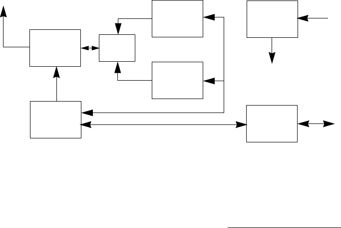
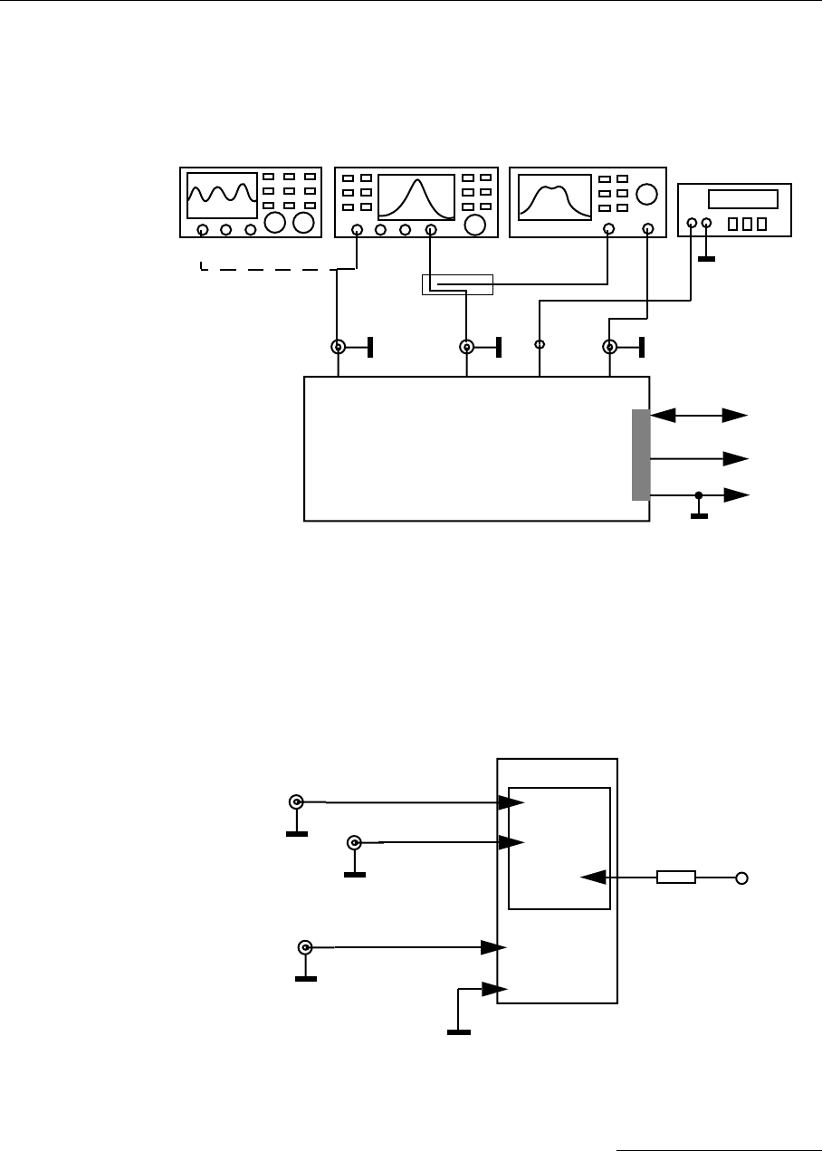
2. Hardware
2.1. Overview
Most of the electronics (including the A431 radio module) are situated on the main
board (for the A431 description, see “The A431 Radio Module” on page 27). The
main board (Figure 1) contains the radio unit, a low-speed and a high speed modem
interface, a microcontroller, RS-485 and RS-232 interfaces and a power conditioning
subsystem. The power and the serial lines are provided over a corresponding con-
nector (4-pin Binder for RS-485 or D-sub 9 pin for RS-232), while the antenna is fed
through a 50
Ω
TNC connector.
Figure 1.
A440 Block Diagram.
A431 Radio
Antenna
µController
Modem
Interface Power
Conditioning
System Supply
Power
Module
Low Speed
Modem
Interface
High Speed
Level
Shifter
RS485/
RS232
Interfaces
Serial

10
Hardware
For further details, consult the schematic diagram in Figure 2.
2.1.1. The Modem Interfaces
The low speed modem operates with two tones: 1 kHz (representing the “1” bits)
and 2 kHz (representing the “0” bits). A bit cell is represented by a complete time
period (
1/f
), thus the raw throughput varies between 1 and 2 kbps (average 1.5
kbps). The modem functions are essentially implemented in software by a separate
microprocessor. However, a signal pre-conditioning is performed on both receive
and transmit paths by means of two low-pass filters (U6 on receive and U19 on trans-
mit).
On receive, the buffered analog data signal from the radio unit is applied to a 3 kHz
low pass filter (U6). The filter output is further fed to the A/D input of a slave micro-
controller U5) performing the decoding operation for the low speed modulation
(see also “Modulation Technique Used (low speed modem)” on page 59). The slave
microcontroller (U5) communicates with the main microcontroller (U9) via a 4-wire in-
terface. In addition, the audio output from the radio unit is also applied to the GMSK
modem (U7) for decoding high speed data.
On transmit, the low speed data is generated again by the slave microcontroller (U5)
added by the R/2R network implementing a D/A converter. The slave microcontrol-
ler generates in effect the sinus waveforms required to encode the binary data. The
output signal is applied to the audio mixer U11, which adds the signal generated by
the high speed modem (U7). Obviously, only one modem will be activated at a time
by the master microcontroller (U9). The output signal of the mixer is applied to the
variable gain amplifier (U15) and then to the final low pass-filter (U19) that has a cut-
off frequency of around 7 kHz.
The high speed modem (U7) has two clocking options: either it can be clocked from
the main microcontroller’s clock via a buffer (U20), or it can be driven by its own
quartz crystal (X3). The low speed modem (U5) is always driven by the main micro-
controller’s clock.
2.1.2. The Microcontroller and the Power Conditioning Sections
The operation of the whole unit is under the control of U9, an Atmel ATMega 103
microcontroller. It is a powerful chip exhibiting a very low power consumption. Its
main functions are:
• Controls the radio unit
• Control the modems functionality
• Assembles the radio frames and waits for requests from a remote
• Implements Adcon radio and RS-485 protocol stack
• Manages the real-time clock

11
The Microcontroller and the Power Conditioning Sections
• Implements a serial Command Line Interface (CLI)
The chip operates at its maximum speed, in this case 4 MHz (the “L” version), and
uses a crystal (X2) for the on-board clock generator. The real time clock is imple-
mented by means of a 32.768 kHz crystal (X1) connected on the internal Timer/
Counter0.
The radio unit is controlled via the SPI bus (to set the PLL chip parameters) and via
several ports of the microcontroller for such operations as transmit and receive. In
addition, the high current 5 volt LDO voltage source (U4) is switched on before the
radio module’s PA is activated. The power output is adjusted by means of an elec-
tronic potentiometer (U2).
The A/D subsystem is used to sample the RSSI and Pout inputs. A stable 2.5 Volt
reference supplied by U3 is applied to the A
ref
pin. The reference is powered by the
microcontroller only when sampling the A/D input.
The serial interface is implemented by means of the built-in UART. Both the RS-232
and RS-485 interfaces are implemented using Maxim chips (U12 and U17 respective-
ly). The serial interface mode is selected by means of a pair of jumpers (J1).
An additional amount of 32Kbytes RAM is provided to the main microcontroller; the
RAM chip (U8) is attached to the multiplexed bus of the microcontroller with the aid
of a latch (U10).
A brown-out supervisor chip (U14) is used to assure a smooth start-up of the micro-
controller and avoid possible erratic behavior when the supply level descends below
the minimum operating value (2.7 volts).
A LDO voltage regulator (U16) is used to provide 3.3 Volt power to the main com-
ponents on the board.
13
The Power Supply and Serial Interface
2.1.3. The Power Supply and Serial Interface
The interface connector allows for:
• External supply (any DC source from 5.6 to 10
volts)
• Communication over serial lines, at 19200 baud
(RS-485).
For testing purposes, Adcon supplies a 220VAC power
adapter that provides also an RS-485 to RS-232 conversion. Thus, the unit can be
connected to a serial port of a PC and can be switched in various operating modes.
A list of commands is given in the sub chapter “Controlling the Unit” on page 50.
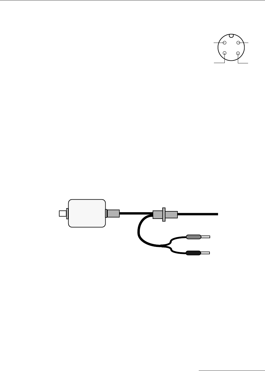
2.1.4. External Power Supply
In order to test the unit over the specified supply range, a special power cable is sup-
plied by Adcon Telemetry. This cable must be connected to the interface connector
of the unit
before
the serial cable (see Figure 3). The two wires with banana plugs
may then be connected to an external variable power supply: the red plug to plus
and the black plug to minus.
WARNING!
Do not apply more than 10 Volts to the unit: permanent damage of the
device may result.
Figure 3.
Connection of an external power supply.
2.2. Specifications
The A440 fulfills the specifications of the EN 300 220-1, Class 12, and ETS 300 113,
as well as the FCC Part 90.214 (Subpart J) of the CFR 47.
1
2
34V+
BA
Gnd
INTERF
+
-
Black
Red
5.6 to 10 Volt
ANT To Interface Unit
A440

14
Hardware
Note: The parameters below were measured with the A440 + A431 combination.
Parameter Min. Typ. Max. Unit
Common
Supply 5.6 6.2 10.0 V
Operating Temperature -30 +70 °C
Relative Humidity 99 %
Class Protection IP65
RF Data Rate (Using the low-speed Modem) 1000 1500
a
a. Data rate is content dependent.
2000 bps
RF Data Rate (Using the high-speed Modem) 8000 bps
Operating Frequency (-44 version)
b
b. This parameter represents the alignment range; the switching range can
be limited in software to a narrower space (even to the extent of a single
channel).
430 450 MHz
Operating Frequency (-46 version)
b
450 470 MHz
Frequency Stability (-20 to +50°C) ±1.5 kHz
Frequency Stability (-30 to +60°C) ±2.5 kHz
Receive mode
Sensitivity (12 db S/S+N) -118 dBm
Image Frequency Attenuation (1st IF = 45 MHz) -70 dB
Local Oscillator Leakage 2 nW
Adjacent Channel Attenuation (12.5 kHz mode) -57 dB
RSSI dynamic 90 dB
Operating Current (incl. On-board Microcontroller) 32 mA
Transmit mode (all measurements made on a 50
Ω
resistive load)
Output Power 27 dBm
Spurious Radiation 200 nW
Adjacent Channel Power (12.5 kHz mode) -34 dBm
Occupied Bandwidth (12.5 kHz mode) 7.0 kHz
Operating Current (incl. On-board Microcontroller) 600 mA
21
A440MB
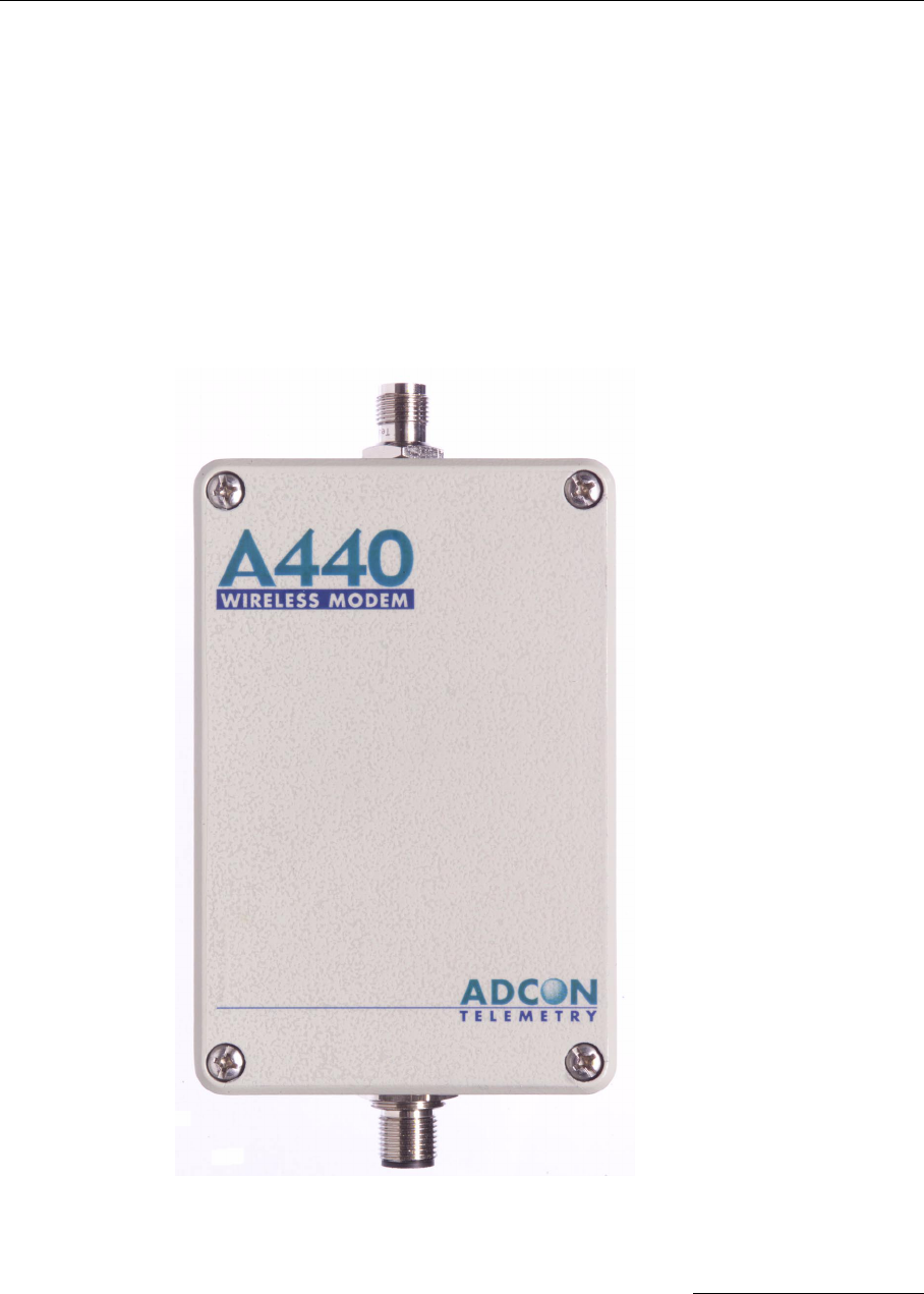
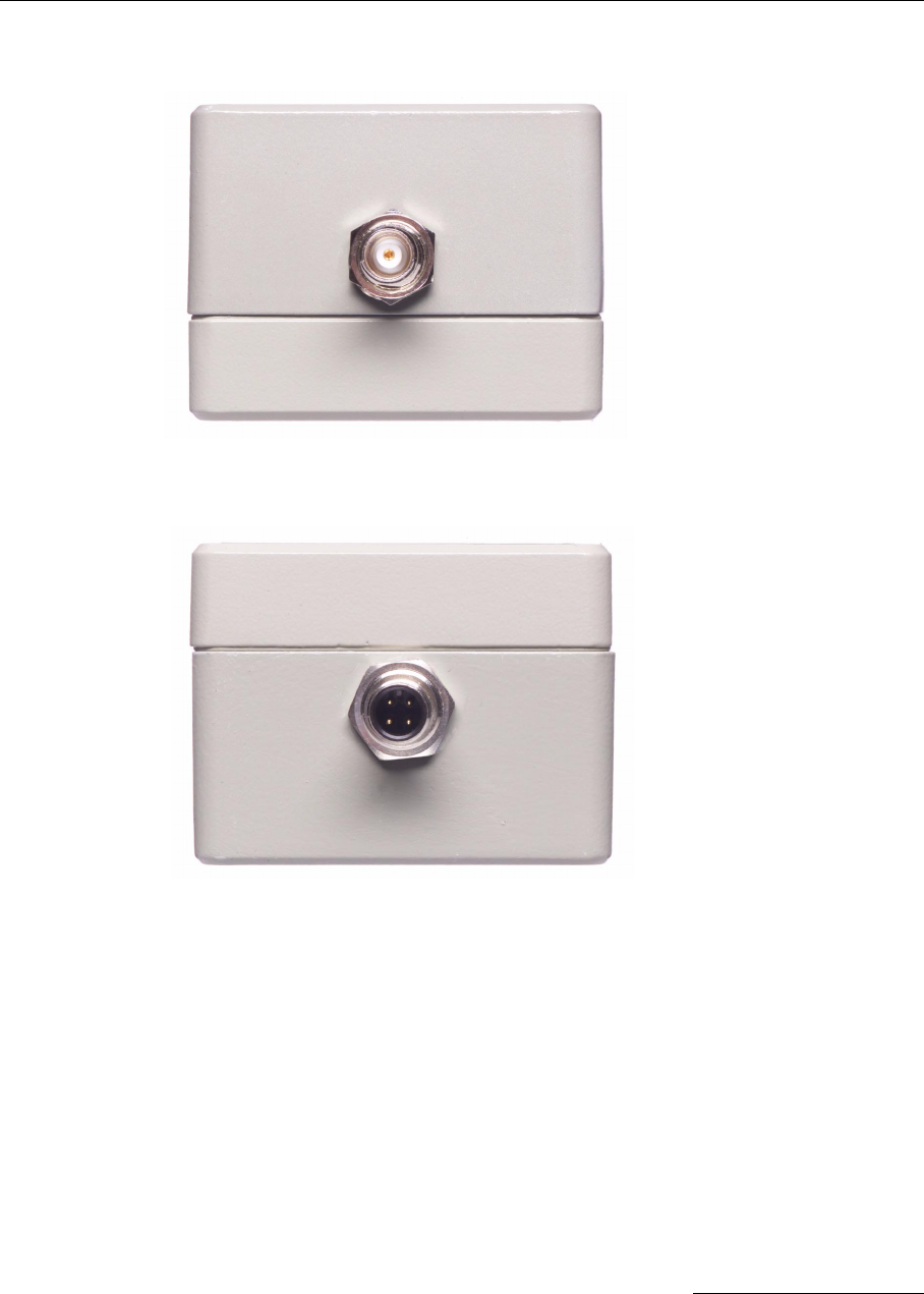
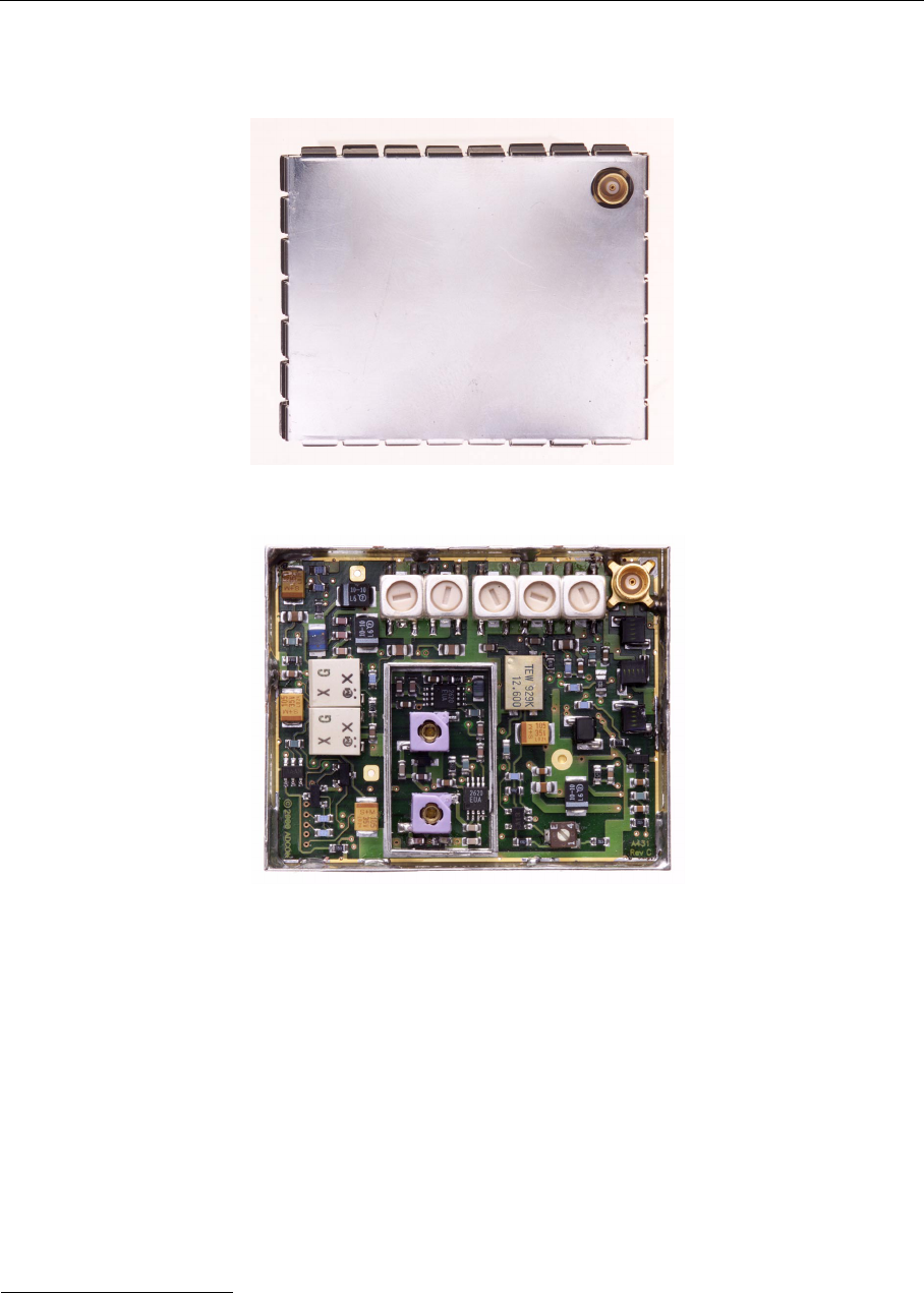
2.5. A440 Device’s Photographs
Figure 6.
A440, Front view.
55 1 XTAL-MC306 32.76KH
zMC-306 X1 Seiko Epson
56 SMD Header 1 SLY8/SMD/055/4 S 2mm J1 Fischer Elektronik
57 Jumper 1 CAB10 2mm to J1 Fischer Elektronik
Pos Description Count Component Name Value Pattern Ref Des Manufacturer
22
Hardware
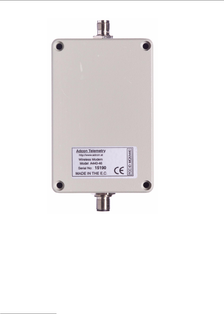
Figure 7.
A440, Back view.
23
A440MB
Figure 8.
A440, Top view.
Figure 9.
A440, Bottom view.
24
Hardware
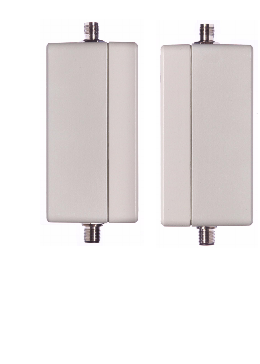
Figure 10.
A440, Left and Right views.
25
A440MB
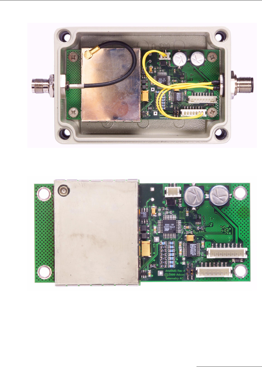
Figure 11.
A440, Case opened.
Figure 12.
A440 Motherboard, top view.
26
Hardware
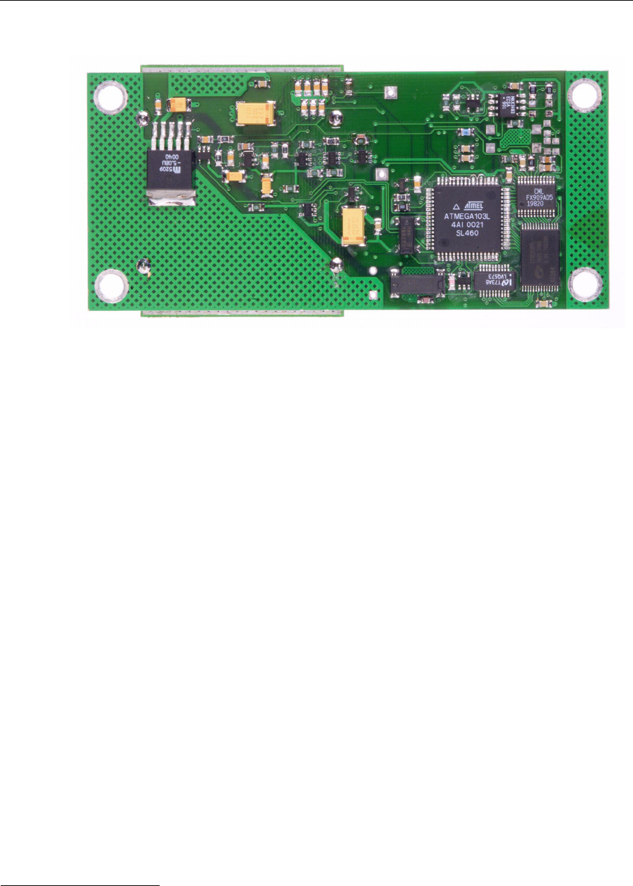
Figure 13.
A440 Motherboard, bottom view.

27
3. The A431 Radio Module
3.1. About the A431 Radio Module
The A431 was specially designed for narrow-band FM data communication. It exhib-
its a relatively flat response in the audio band from 10 Hz to 2.5 kHz, both on send
as well as on receive paths. Additionally, the receiver’s group delay is very low.
The module operates in the 430 to 470 MHz range, making it compatible with most
radio communication regulations in the world. The output power is 0.5 W, while the
modulation is narrow-band FM (12.5, 20 or 25 kHz channel spacing). The power con-
sumption in receive mode is remarkably low (under 32 mA), in spite of the good IP3
characteristics and high sensitivity. The switching from receive to transmit is fast, un-
der 20 mS.
3.2. Functional description
The following functional description refers to the schematic diagram in Figure 14.
3.2.1. Receiver Section
The antenna signal is fed through the common low-pass filter for both receive and
transmit and applied to the U3 antenna switch. From the J3 port of the switch, it is
then fed to the FL1 helical filter and amplified by the LNA built with Q2 that assures
a high amplification factor (over 20 dB). Another helical filter follows (FL2), giving a
total of more than 70 dB attenuation of the first image frequency.

28
The A431 Radio Module
The incoming signal is then applied to the first mixer, U7, through an LC impedance
matching network (L12/C48). The local oscillator signal is obtained by means of the
VCO built around U10 and applied to the mixer (the LO has a lower frequency than
the incoming signal). The VCO is locked to the OSC1 reference by means of the U9
dual-PLL chip.
The mixer’s output on 45 MHz is filtered by means of XF1, which is needed to ensure
a sufficient attenuation (over 70dB) of the second image frequency (at 44.090 MHz).
The second local oscillator is built around the IF chip, but it is locked by means of
the second PLL of U9. In this way, all signals are generated from a common reference
oscillator (OSC1, see also “Frequency Reference Specifications” on page 45).
The IF chain chip amplifies the signal to a proper level for FM detection. A particu-
larity of this chip is that the FM detector is PLL-based, thus no coils or ceramic dis-
criminators are needed. Two ceramic filters, CF1 and CF2, ensure the required
adjacent channel separation. The audio output is delivered on pin 17 and is slightly
amplified through U11 in order to bring it to 1Vpp, and centered on half the supply
voltage (which is 3.3 volt approximately). The audio signal is fed out of the module
on the pin
RXDO
of the interface connector. In addition, an RSSI level signal is ob-
tained on pin 18 of U8 and is fed to switch U6. As long as the module is in receive
mode, the RSSI signal will be present on the
RSSI/PO
pin of the interface connector.
3.2.2. Transmitter Section
The carrier is generated directly on the operating frequency by means of the VCO
built around U2. The signal is locked on the reference OSC1 with the aid of the dual
PLL chip based on U9. The chip, a National Semiconductor LMX2332L, was chosen
for its fast locking scheme, low power consumption, and good RF characteristics.
The modulation is applied on both the VCO and the reference, in order to attain a
flat characteristic in the whole band (10 Hz to 2.5 kHz). Due to the phase differences
between the two modulation points, the signal applied on the reference is inverted
by means of U4. Meanwhile, U4 is used to center the reference on the channel (using
the trimpot R75). The PLL low-pass filter (third-order) composed of C66/C67/R69/
R59/C64 is calculated around 400 Hz. R64 is used for the FastLock® mechanism.
(For further details on the FastLock mechanism, please consult the National Semi-
conductor documentation.)
The signal is pre-amplified to approximately 0 dBm by Q1 and then it is applied to
the PA built with U1. The output signal is pre-filtered and impedance-matched by
means of theC21/L10/C22 low-pass filter and then fed to the antenna switch. Before
reaching the antenna output, a three-cell, low-pass filter (used also on the receive
path) is used to attenuate the unwanted harmonics and keep them below the re-
quired limits.

30
The A431 Radio Module
An Automatic Level Control (ALC) system is responsible for keeping the output pow-
er constant, regardless of the external influences (temperature, VCO excitation and/
or supply). A small part of the RF energy is rectified by D2 and applied to the U5:A
amplifier. By means of U5:B, the power is controlled according to the pre-set power
level (ALC input). U5:A is basically an analog comparator between the actual and the
programmed power output. Depending on the error signal obtained, a variable volt-
age is applied on the PD input of the PA chip, thus effectively controlling its output
power. In addition, the actual power output level is fed to the U6 analog switch and
presented to the RSSI/PO output while the unit is switched in transmit mode.
The modulation is applied on two-points: the VCO and the reference oscillator—this
is needed to obtain a flat response in the audio range from 10Hz to 2.5 kHz and com-
pensate for the counter-effect opposed by the synthesizer loop. The input signal
(must be 1 Vpp) is fed through a resistive divider (R14/R13) to the “cold” end of the
varactor diode controlling the VCO (D1). At the same time, the same modulation
signal is applied to the inverting op-amp U4 and then to the OSC1 reference oscil-
lator (a VCTCXO). The modulation signal is inverted in order to bring it in phase with
the VCO modulation point.
3.3. Manufacturing Issues
3.3.1. Marking and labeling issues
The A431 Module is manufactured in two versions:
• Low band—able to operate between 430 and 450 MHz
• High band—able to operate between 450 and 470 MHz
From a manufacturing perspective, the difference between the high and low band
are the two helical filters FL1 and FL2 used on the receiving chain. The low band ver-
sion is marked as A440-44 while the high band is marked as A440-46 (when the
modules are included into the A440 Wireless Modem).
3.3.2. Alignment Range and Switching Range
The A431 radio module’s alignment range is 20 MHz, while the switching range is
10 MHz. According to the definitions formulated in the ETS 300220 and ETS 300013
specifications, the A431 radio module (combined with the A440 Wireless Modem)
belongs to the AR1 category. Therefore, for the European testing, two units should
be presented for test purposes, as follows:
• One A440 unit containing an A431-44 radio module, alignment range 430-
450 MHz, switching range 433-443 MHz
• One A440 unit containing an A431-46 radio module, alignment range 450-
470 MHz, switching range 455-465 MHz.

31
Tuning Procedure
Consequently, two test reports will be provided to Adcon Telemetry AG.
For North America (FCC), only the portion 460 to 470 MHz will be used; therefore,
a single device model A440-46 having the switching range between 460 and 470
MHz will be submitted for testing.
3.3.3. Tuning Procedure
The A431 modules are to be tuned by mounting them on a test fixture consisting of
a specially modified A733 motherboard (the A733 is an universal low cost Remote
Telemetry Unit manufactured by Adcon). The modification refers to certain mechan-
ical aspects, in order to provide an easy plug in and out of the control connector (P2)
as well as to the TP1 and TP2 test points.
The alignment operation must differentiate between following classes of units:
• Band 1: from 430 to 440 MHz
• Band 2: from 440 to 450 MHz
• Band 3: from 450 to 460 MHz
• Band 4: from 460 to 470 MHz
Note: The boards differ only through the FL1 and FL2, in that Band 1 and 2 use
models TOKO 493S-1071A and 492S-1056A while Band 3 and 4 use models
TOKO 493S-1075A and 492S-1060A, respectively. In addition, the tuning pro-
cedure and some software parameters differ. The differences are clearly stat-
ed in the following paragraphs, where applicable.
Note: Special versions could also be delivered having switching ranges in-between
those defined above; however, it may never exceed 10 MHz.
3.3.4. Setting Up the Default Parameters
The tuning procedure is not possible without first configuring some default param-
eters for the A733 motherboard used in the testing fixture. This is done via the serial
interface of the motherboard by using a communication terminal program (e.g. Hy-
perterminal, in Microsoft® Windows™ 95). The terminal program must be config-
ured as follows:
• 19200 Baud
• 1 Stop bit
• No parity
• No protocol (neither hardware, nor software)
To check if the communication is operational, press the
ENTER key. An
nnnn 0
RxD
TxD
Ground
Battery
Ext Power
1
2
3
4
5

32
The A431 Radio Module
#
prompt should appear on the terminal screen (nnnn is the actual ID of the unit that
is printed on its label). The following default parameters must be pre-loaded (for
more information about the meaning of the commands, consult the section “Com-
mands” on page 51):
Commands valid for all bands
ID 1
PMP 65 72
SLOT 900 15
RSSI 58
Commands required for band 1
SR 430000000 440000000
BL 430000000 440000000
FREQ 435000000 12500
Commands required for band 2
SR 440000000 450000000
BL 440000000 450000000
FREQ 445000000 12500
Commands required for band 3
SR 450000000 460000000
BL 450000000 460000000
FREQ 455000000 12500
Commands required for band 4
SR 460000000 470000000
BL 460000000 470000000
FREQ 465000000 12500
Note: The SR command sets the switching range limits, the BL command sets the
band limits, and the FREQ command sets the actual operating frequency;
before shipping and depending on the target country, these parameters may
be changed. The SL command must be always issued before the BL com-
mand and the BL command must always be issued before the FREQ com-
mand.
33
Definitions
3.3.5. Definitions
The diagram of the setup environment is depicted in Figure 15.
Figure 15. Trimming Setup.
The testing fixture is used to fasten the A431 Module under test both mechanically
and electrically in such a way as to allow its rapid and comfortable alignment. It con-
sists of a mechanical board with two screws that are used to fasten the board; two
elastic pins are used to transport the relevant signals from the module to their cor-
responding test cables. The directional coupler connects the antenna input/output
of the device under test to both the network analyzer and the service monitor. The
schematic diagram of the testing fixture is depicted in Figure 16.
Figure 16. Schematic Diagram of the Testing Fixture.
0.765 V
Out
Scope Ant I/O Out
Voltmeter Out
Network
Analyzer
Testing
Fixture
RS232 To/From PC
+
–
6.5 V
A733MB
Connector
Optional
Scope Service Monitor Network Analyzer Voltmeter
Directional Coupler
Scope
Out Network
Analyzer
Ant
Gnd
TP1
A733MB
TP2
TP2 Voltmeter
470KΩ
Antenna
A431
Module

34
The A431 Radio Module
3.3.6. Test Equipment Settings
Before proceeding, certain controls on the test equipment must be set; some of the
settings depend of the operating band (high or low) of the device under test (DUT).
In addition, it is highly recommended that the ambient temperature during align-
ment is kept to 22° C (±1°C).
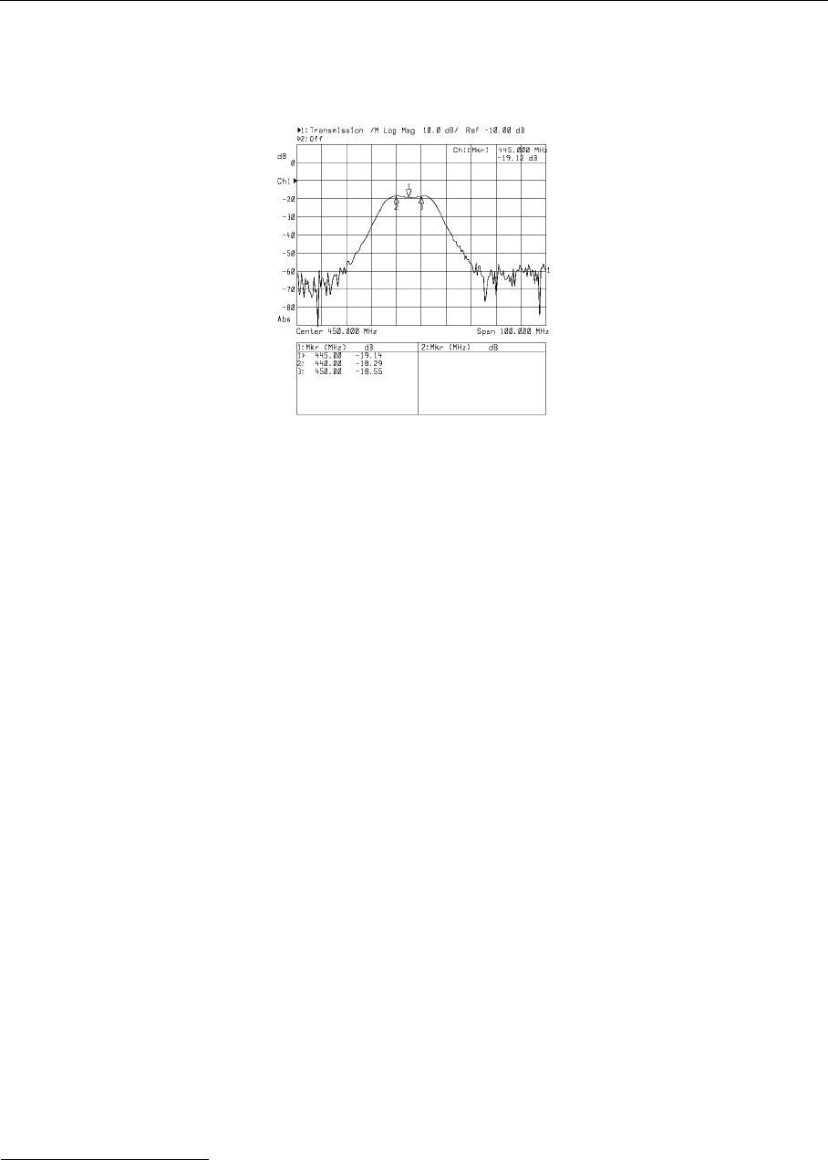
3.3.6.1. Network Analyzer (HP 8712 or equivalent)
The settings for the Network Analyzer are as follows:
• Center frequency: 450 MHz
• Span: 100 MHz
• Display: 10.0 dB/div
• Power: -20 dBm
• Markers:
— band 1: Mkr1 – 435 MHz, Mkr2 – 430 MHz, Mkr3 – 440 MHz
— band 2: Mkr1 – 445 MHz, Mkr2 – 440 MHz, Mkr3 – 450 MHz
— band 3: Mkr1 – 455 MHz, Mkr2 – 450 MHz, Mkr3 – 460 MHz
— band 4: Mkr1 – 465 MHz, Mkr2 – 460 MHz, Mkr3 – 470 MHz
Note: It is a good idea to store the instrument state for the four settings for a rapid
recall when needed.
3.3.6.2. Service Monitor (Rohde & Schwarz CMS50 or equivalent)
The setting for the receiver section check are as follows (RX-TEST):
• SET RF: 435000000 Hz (Band 1) / 445000000 Hz (Band 2) / 455000000 Hz
(Band 3) / 465000000 Hz (Band 4)
• RF LEV: -118dBm
• SINAD
• AF1: 1kHz
• MOD1: 2.5 kHz
• SCOPE MODE
• BEST RANGE
The settings for the transmitter section check (TX-TEST):
• COUNT: (should show the transmitter carrier frequency)
• POWER: (should show the transmitter carrier power)
35
Trimming Elements
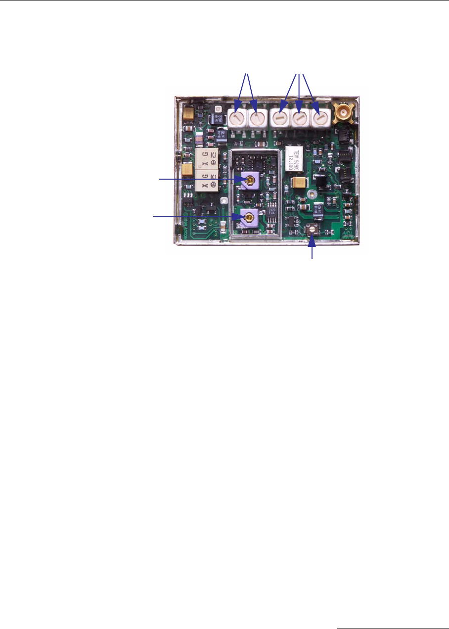
3.3.7. Trimming Elements
The location of the trimming elements on the A431 Module is shown in Figure 17.
Figure 17. Location of the trimming elements.
3.3.8. Adjusting the Receiver Front End
1. Mount the DUT (Device Under Test) on the testing fixture and connect it to the
host via the serial cable.
2. Select the appropriate instrument profile depending on the device’s band.
3. Turn the DUT in permanent receive mode by entering the RX command at the
terminal.
4. Adjust the FL1 and FL2 filters (see Figure 17) until you obtain a curve similar to
the one shown in Figure 18 (depending on the band, the markers may be
different); this is done by successively adjusting the five trimming screws
located on the filters.
R75 (Crystal Reference)
FL1FL2
L15 (RX VCO)
L7 (TX VCO)
36
The A431 Radio Module
If the adjustments do not achieve the appropriate curve, check the power supply,
the cable connections to/from the test equipment, etc. Verify also that all the pins of
the FL1 and FL2 filters are properly soldered.
Figure 18. Helical Filter + LNA’s selectivity diagram.
3.3.9. Adjusting the VCOs
1. Verify that the DUT is in receive mode (enter the RX command at the terminal
program).
2. Adjust the coil L15 (see Figure 17) until the voltage shown on the digital
voltmeter is 1400 mV, ±50 mV (see also the note below).
3. Switch the unit to transmit mode by entering TX at the terminal.
4. Adjust the coil L7 (see Figure 17) until the voltage shown on the voltmeter is
again 1400 mV, ±50 mV.
5. Press the enter key at the terminal to switch the unit off.
Note: A one-time calibration of the Testing Fixture may be needed due to the in-
ternal resistance of the voltmeter and the serial resistor mounted on the Test-
ing Fixture. The calibration is performed by measuring the VCO voltage
directly on the TP2 and by comparing the value with that measured through
the Testing Fixture. The values given above are the real ones, measured di-
rectly.
If the above limits cannot be obtained, or the readout is unstable, verify the follow-
ing:
• The programmed operating frequencies are indeed 435 (Band 1), 445
(Band 2), 455 (Band 3) and 465 MHz (Band 4). To check this, type the com-
mand FREQ at the terminal prompt; the device will answer by returning the
current frequency.
• The respective commands (RX and TX) were issued.

37
Adjusting the Crystal Reference
• No parts are missing, or have the incorrect value, or are badly soldered (check
the parts around U2 and U10).
3.3.10. Adjusting the Crystal Reference
1. Switch the unit to transmit mode by entering TX at the terminal.
2. Observe the indication shown by the Service Monitor: adjust R75 (see
Figure 17) until the carrier frequency indicates 435000000 (Band 1), 445000000
(Band 2), 455000000 (Band 3), or 465000000 MHz (Band 4) ± 200 Hz,
respectively.
3.3.11. Checking the Receiver Parameters
1. Switch the DUT to receive mode by entering RX at the terminal.
2. Switch the Service Monitor to RX TEST mode, on the appropriate frequency
(435 / 445 / 455 or 465 MHz respectively); the level should be -118dBm (see
also “Test Equipment Settings” on page 34).
3. Verify that the S/N ratio is at least 12 dB; in addition, if a scope is also
connected, a clear 1 kHz sine wave should be visible, with a relatively low
amount of noise superimposed.
4. Switch the DUT to pulsed mode by pressing the Enter key. After several
seconds, you will see the image on the scope pulsing at about one-second
intervals.
5. Switch the RF generator output off.
6. Verify that the RSSI threshold is correct by typing the command RSSI; the actual
value must be lower than the threshold set. If this is not the case, repeat the
RSSI command several times—perhaps the frequency is in use (a radio receiver
set on the operating frequency would help detect foreign transmissions). If the
threshold difference is marginal, it must be increased by using the RSSI
<value> command (it must be 20 to 30% higher than the actual value).
If any of the above targets are not reachable, visually verify first that the U8 chip is
correctly soldered and that there are no shorts between its pins (most problems usu-
ally appear around this chip).
3.3.12. Checking the Transmitter Parameters
1. Switch the DUT to transmit mode by typing the command TX 0 at the terminal.
2. Switch the Service Monitor to TX TEST mode, on the appropriate frequency
(435 / 445 / 455 or 465 MHz respectively). You should see the following
parameters on the Service Monitor readout:
a. Carrier: 435000000 ± 200 Hz (or 445000000 / 455000000 / 465000000
respectively)
b. Output Power: 26.5 dBm (+ 0.5 dBm / - 1 dBm)

38
The A431 Radio Module
c. Frequency Deviation: ±1.5 kHz (±0.2 kHz)
3. Switch the unit to stand-by by pressing the Enter key.
For item 3.a above, adjust R75 (see Figure 17). For item 3.b, issue the command
PWR at the terminal and use the D (down) and U (up) keys until the required value
is reached. Finally, for item 3.c, issue the command BW at the terminal and again
use the D and U keys to reach the required value.
3.3.13. Data Transfer Check
The last check is a radio data transfer. In order to perform it, at least a base station
(model A730SD) or a remote station (model A733) must be installed and operated
on the same test frequency, in the near vicinity (no more than 30 m).
Note: The base or remote station used for this test must be operated with a fictive
antenna (a 50Ω resistor).
To perform the test, enter the command B at the terminal prompt: the base and/or
remote station must answer with the RF in and out values. If an answer is not re-
ceived after several seconds, retry the command. If an answer is still not received,
then use a scope on TP1 on the A733MB board (the Text Fixture) to verify that the
digital data is present (on receive). In addition, a radio receiver tuned on the oper-
ating frequency can also supply a rough indication of whether the receiver or the
transmitter is defective.
45
Data Transfer Check
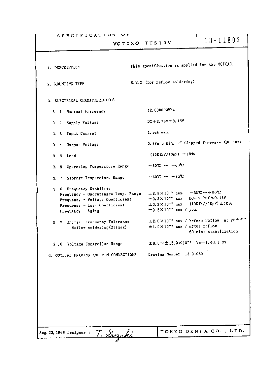
3.6. Frequency Reference Specifications
46
The A431 Radio Module
3.7. A431 Module’s Photographs
Figure 21. A431 Module, General view.
Figure 22. A431 Module, Top view.
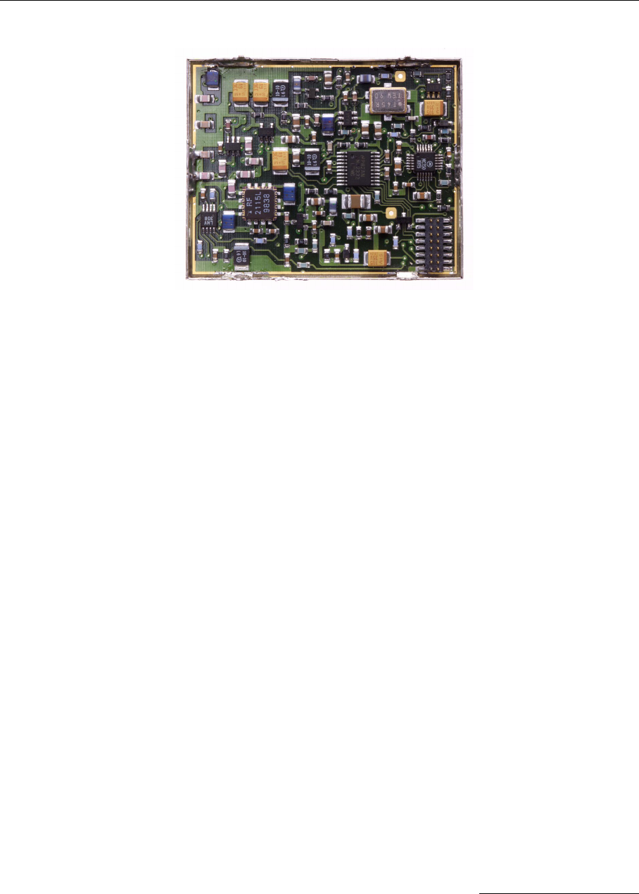
47
Data Transfer Check
Figure 23. A431 Module, Bottom view.

48
The A431 Radio Module

49
4. Software
4.1. Short Description
The software is written entirely in C. It consists of a collection of standard C library
functions, a preemptive multitasking operating system (CMX) offering basic config-
uration and administration functions (including a command line terminal on a serial
port), and the application software itself, which assures the desired functionality of
the device.
4.2. Tasks
Following tasks are currently implemented:
• Command Line Interpreter Task
• Radio Task
• Real Time Clock (RTC) Task
The system usually remains in sleep mode. Each 0.5 seconds, an interrupt is gener-
ated by the local 32.76 Khz crystal oscillator. This wakes up the processor and acti-
vates the CMX RTOS, which allows all active tasks to perform their functions. After
all the tasks have finished their jobs, CMX brings the system back to sleep. The 0.5
seconds interrupt routine is also used as time reference for the RTC task.
One of the main concerns of the software design is the power consumption of the
device. The software must ensure that all the peripherals are left in the correct state
in order to reduce their consumption to a minimum; all operations are executed in
the shortest possible time.

50
Software
4.3. Controlling the Unit
The unit under test can be controlled by means of the special adapter box A720PS
that supplies the unit on one hand, and performs the RS-485 to RS-232 signal con-
version on another hand. The serial output of the box can be connected to a PC (e.g.
a laptop) by means of a null modem cable. In order to switch the unit to various
modes of operations, a simple communications terminal program will suffice (e.g.
Terminal or Hyperterminal in Windows, or tip/cu under Unix). The terminal program
must be configured as follows:
• 19200 Baud
• 8 Data Bits
• No Parity
• 1 Stop Bit
• Force LF after CR
4.3.1. Serial Communication Protocol
This protocol is based on a master sending commands and a node answering; the
whole communication is conducted in plain ASCII, as strings. When exchanging
numbers, they are represented in decimal format. All commands are terminated with
a CR/LF combination. All responses (answers) are terminated with the # character.
4.3.2. General Format of a Command
The commands have the following format:
ID Command Param1 Param2 ... ParamN
•ID is the destination device. If you include an ID as part of a command, the
node checks whether ID=ownID. If it does, the node executes the command
on itself. If the ID is not the node’s ID, the node executes the command on a
remote device, if such an ID exists. If the ID is missing, this implies that the
command is addressed locally.
Note: Not all the commands can be relayed remotely.
•Command is the command proper, which can be composed of a variable string
of characters (for example, SLOT). Each node can implement a set of com-
mands depending on the functionality of the node itself. However, as a mini-
mum requirement, a node recognizes the CMDS command, which returns a list
with the commands recognized by the node.
•Param1 Param2 ... ParamN represent the parameters, which are com-
mand dependent. If you type no parameters when you issue a command, it is
the equivalent of querying for information (the GET version of a command). If
you type parameters, you are issuing the SET version of a command and are
setting the command to the parameters you typed.

51
General Format of an Answer
4.3.3. General Format of an Answer
The answers have the following format:
ID Command Result1 Result2 ... ResultN ErrResult #
•ID is the answering device. If a command was further routed, it is the ID of
the end device. The answer must always contain the ID on return.
•Command is the string representing the original command. It is supplied so
that a master can distinguish between the answers it is waiting for, and out-
of-band notifications (which may come, for example, over the radio port of a
node). As with the ID, the command name must be always supplied.
•Result1 Result2 ... ResultN are the result values returned by the re-
mote node. If the ErrResult is not zero, all other possible characters and/
or strings until the end of the line may be ignored.
•ErrResult shows whether the command was successfully executed. If this
value is 0, the command was successfully executed. If this value is other than
0, the command failed. The number may further indicate the error type. (See
also “Returned errors list” on page 56.)
The answer string may contain any number of spaces or CR/LF characters between
its components; however, after the terminator (#) no other characters are allowed.
4.3.4. Commands
Both uppercase and lowercase characters can be typed because the commands are
not case sensitive. The commands list is not exhaustive, only those commands
deemed necessary for type approval testing were included.
CMDS
DESCRIPTION Returns a list of supported commands.
PARAMETERS None.
REMARKS GET only.
RETURNS A list of strings separated by spaces.
REMOTE No.
EXAMPLE
CMDS
193 CMDS CMDS ID PMP RSSI TIME FREQ DEV DEL REPL SLOT DATA INFO RX TX ERA 0
#
TIME
DESCRIPTION Sets/returns the real time clock.

52
Software
PARAMETERS The actual time, or none in the GET version.
RETURNS The actual time as dd/mm/yyyy hh:mm:ss.
REMARKS GET/SET.
REMOTE No.
EXAMPLES
TIME 12/12/1999 22:10:10
193 TIME 0
#
TIME
193 TIME 12/12/1998 22:10:10 0
#
SR
DESCRIPTION Sets/returns the band switching limits.
PARAMETERS The switching band limits (Hz), or none in the GET version.
RETURNS The actual frequency band limits, in Hz.
REMARKS GET/SET. This is a hidden command (i.e. not available for the normal user in the
CMDS list).
REMOTE No.
EXAMPLE
SR 432000000 450000000
193 SR 0
#
BL
193 SR 432000000 450000000 0
#
BL
DESCRIPTION Sets/returns the band limits.
PARAMETERS The frequency band limits (Hz), or none in the GET version.
RETURNS The actual frequency band limits, in Hz.
REMARKS GET/SET. This is a hidden command (i.e. not available for the normal user in the
CMDS list).
REMOTE No.
EXAMPLE
BL 432000000 450000000
193 BL 0
#
BL
193 BL 432000000 450000000 0
#

53
Commands
FREQ
DESCRIPTION Sets/returns the operating frequency.
PARAMETERS The operating frequency and step (Hz), or none in the GET version.
RETURNS The actual frequency and step, in Hz.
REMARKS GET/SET.
REMOTE Yes, SET only.
EXAMPLE
FREQ 433925000 25000
193 FREQ 0
#
FREQ
193 FREQ 433925000 25000 0
#
DATA
DESCRIPTION Returns data stored for a certain device.
PARAMETER The ID of the device for which the data is requested and the date/time (in the stan-
dard format) the data was stored. If missing, it refers to the data of the local device.
RETURNS A data block.
REMARKS GET only. If the date/time parameter is not included, the latest data is returned. If
the date/time parameter is included, the date and time closest to, but later than, the
given date/time is returned.
REMOTE Yes, for a GET, but only one frame at a time. The A440 implements only the remote
version.
EXAMPLE
DATA 193 12/12/1998 12:12:12
193 DATA b1 b2 b3 ... bn 0
#
The data block returned will typically contain a number of data frames (telegrams).
The structure of a block is as follows:
dd mm yyyy hh mm ss si ft d1 d2 ... dn dd mm yyyy ... dn cs
where:
•dd mm yyyy is the date
•hh mm ss is the time
•si is the size of the frame
•ft is the frame type
•d1 d2 ... dn are the data values (the frame content)

54
Software
•cs is a 16-bit checksum obtained by summing the bytes and discarding the
carries over 0xFFFF
The remote version is limited to a single frame. An example of such a command is
given below:
9999 DATA 9999 30/9/1999 14:50:00
9999 DATA
30 9 1999 14 54 55 21 37 255 255 77 0 0 0 0 89 156 126 20 0 0 0 0 0 0 0 0 0 3197 0
#
Notice that if you need to get data that is not the last (newest) slot remotely from a
device, the ID must be supplied twice. If you need to get the last slot stored, you
can ignore the ID and the date/time parameters:
9999 DATA
9999 DATA
13 9 1999 19 26 36 21 37 255 255 79 0 0 0 0 87 148 149 15 0 0 0 0 0 0 0 0 0 3148 0
#
INFO
DESCRIPTION Returns various status information.
PARAMETERS None.
RETURNS A list of a device’s internal variables:
ID INFO rf_in rf_out date time ver clk stack cop batt temp days_uptime
hr:min_uptime rssi pmp_low pmp_high type slot samples err_level
#
The formats for the above parameters are as follows:
•rf_in and rf_out as a decimal (unsigned char)
•date as dd/mm/yyyy
•time as hh:mm:ss
•ver as x.x
•clk, stack, and cop as decimal (unsigned char); they represent internal
housekeeping parameters: the A440 uses cop to number watchdog occur-
rences, but clk and stack are currently undefined
•batt as battery level using the standard voltage conversion equation (0 is 0
volts, 255 is 20 volts)
•temp as internal temperature in the housing, which is device dependent. The
precision of the sensing element is usually low (±2°C to ±4ºC, depending on
device), but it is sufficient for battery power management (charge/discharge).
To compute the actual value (in °C), the particular conversion equation for
each device must be used (check the respective device’s manual). The A440
does return always 0 (no temperature measurement)

55
Commands
•days_uptime in days; together with hr:min_uptime, it represents the
amount of time the device is up without a reset or watchdog
•hr:min_uptime in hours:minutes format
•rssi as decimal (unsigned chars); it is the programmed value with the RSSI
command
•pmp_low and pmp_high are the programmed values with the PMP com-
mand
•type is used to represent the device type; following types are assigned cur-
rently:
— 0 for A730MD
— 1 for A720
— 2 for A730SD
— 3 for A720B
— 4 for A733
— 5 for A723
— 6 for A440
•slot and samples are the actual values programmed by means of the SLOT
command
•err_level is the error value; 0 means no error
REMARKS GET only.
REMOTE Yes, GET only. The A440 can issue the command both remotely and locally.
EXAMPLE
INFO
193 INFO 255 0 18/4/1999 21:5:11 1.3 0 0 0 91 72 40 1:46 58 65 72 3 900 15 0
#
RX
DESCRIPTION Switches the unit to permanent receive mode (for tuning purposes).
PARAMETERS None.
RETURNS Nothing.
REMARKS The system stops, and exits the command only when a key is pressed. This com-
mand returns no message.
REMOTE No.
EXAMPLE
RX
193 RX 0
#
TX
DESCRIPTION Switches the unit to transmit mode (for tuning purposes).

56
Software
PARAMETERS None (sends an unmodulated carrier), 1 (sends a 1 kHz modulated carrier), 0 (sends
a 2 kHz modulated carrier) or 5 (sends a mixed 1 + 2 kHz modulated carrier).
RETURNS Nothing.
REMARKS The system stops, and exits the command only when a key is pressed. This com-
mand returns no message.
REMOTE No.
EXAMPLE
TX
193 TX 0
#
TX 1
193 TX 0
#
TX 5
193 TX 0
#
B
DESCRIPTION Sends a broadcast frame.
PARAMETERS None.
RETURNS A data block.
REMARKS After the device sends the broadcast frame, it will listen for answers. All valid an-
swers will be listed with their IDs.
REMOTE No.
EXAMPLE
B
193 B 0
#234 BA 0
#7851 BA 0
4.3.5. Returned errors list
Following are error messages you might get.
Command line interpreter
• 1 — nonexistent command
• 2 — command line buffer overflow (input line too long)
• 3 — internal error
• 4 — reserved
• 5 — missing or false parameters in command

57
Returned errors list
• 6 — operation not implemented
Device descriptors and storage handler
• 10 — device not found (attempt to perform a command on a nonexistent de-
vice)
• 11 — device already exists
• 12 — reserved
• 13 — no more space for descriptors (too many devices)
• 14 — no more records for the specified device
• 15 — temporary communication break, no more data (the last request was not
successful)
• 16 — time-out (the handler blocked or is busy)
• 17 — internal error
• 18 — attempt to insert a reserved device ID number (0 or 65535)
Real time clock
• 20 — incorrect time supplied (no conversion to time_t was possible)
Radio interface
• 30 — error at receive (CRC, etc.)
• 31 — unexpected frame received
• 32 — wrong length
• 33 — reserved
• 34 — reserved
• 35 — time-out (remote device not responding)
• 36 — receiver busy (for example, just making the request round)
Notifications
• 40 — request to read a notification when no notification is pending
4.4. Adcon Packet Radio Protocol
The A440 is basically intended as an end device in a radio network. Most frames de-
fined by the Adcon Packet Radio Protocol are recognized and answered by an
58
Software
AA440. In addition, full source routing of frames for other destinations is implement-
ed.
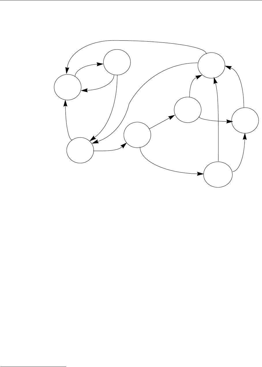
Figure 24. State Transition Diagram of the radio communication task.
4.4.1. Digital Squelch
In order to reduce the power consumption during receive mode, the unit uses a pro-
tocol originally developed by Adcon Telemetry for the A730 family, but with some
additional refinements to further reduce the power consumption. The receiver is
pulsed at a 0.5 seconds interval. At wake-up, the receiver samples first the RF chan-
nel for a carrier, by measuring the RSSI. The RSSI output is extremely stable due to
the wide dynamic range that the IF chip exhibits (over 100 dB, temperature compen-
sated). If the sampled RSSI is under a preset threshold, the unit will immediately go
back to sleep. This procedure takes under 20 mS, typically (from wake-up to result).
If, however, an RF level superior to the preset threshold is detected, the micropro-
cessor will try to detect a valid header, which is composed of a 2 kHz tone of at least
0.5 seconds long. The tone detection is performed by the microcontroller in soft-
ware, and takes at most 6 additional milliseconds. If no valid tone is detected, the
unit goes back to sleep, otherwise it tries to decode the frame.
Based on the destination ID, the frame will be identified. If it is not for that particular
unit (own ID), then the microcontroller will cease decoding it and will go immediately
Idle
Measure RF
Check
Destination
No Signal
0.5 sec
Interrupt
Header Detected
Not for us
Get Frame
We are called
New Frame Possible
Wait
Nhops + 1 s
and
Hunt Syncs
Timeout Expired
Answer
Appropriately
Ack
Resend
Frame with
Long
Header
Frame Sent Twice
No Ack
Payload is for us
Must route
Update
Header
and Send
Ack
No Ack
59
Modulation Technique Used (low speed modem)
to sleep. The destination ID is positioned very early in the frame header (see also
“Generic Format of a Radio Frame” on page 59).
From the above it becomes clear that in order to initiate a communication, a re-
quester must send first a header which is at least 0.5 seconds long: these are called
long header frames. Of course, after the communication is established the headers
are short, of only 16 bytes (i.e. 8 msec. – called short header frames). If a timeout
occurs, the system will restart by sending long header frames.
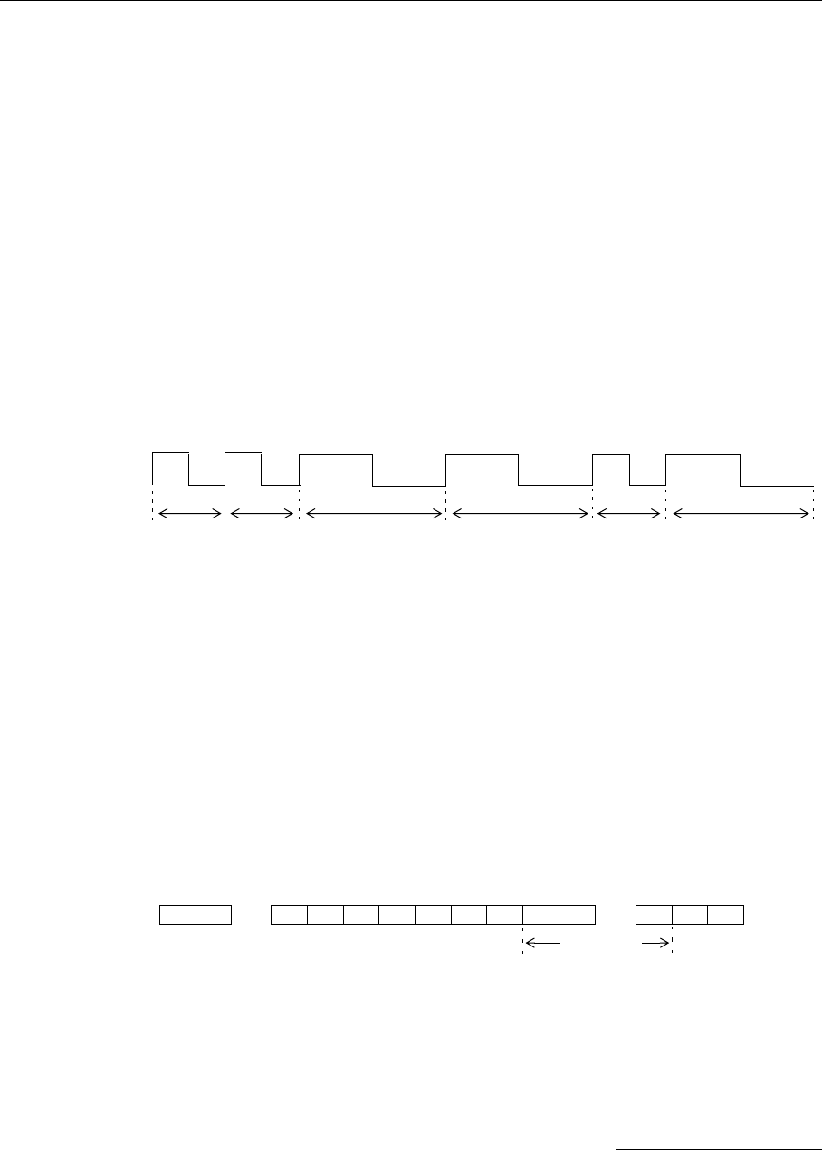
4.4.2. Modulation Technique Used (low speed modem)
The communication via radio is made by using a special MSK (Minimum Shift Keying)
scheme; both the encoding and the decoding of the MSK frames is made in soft-
ware—there is virtually no hardware modem. A zero bit is transmitted as a sequence
of 250 µs one level followed by a 250 µs zero level, while a one bit is transmitted as
a 500 µs one level followed by a 500 µs zero level. A complete sequence of one and
zero level forms a bit cell.
This modulation scheme is self-clocked. The transmission speed is content-depen-
dent, varying from 1 kbps (when sending only ones) to 2 kbps (when sending only
zeros). On the average, an 1500 bps transmission speed is reached.
The data interchange between stations is made by means of frames. The frames
have a header, a 16 bit-sync character, a data block, and a 16-bit CRC number. The
bytes forming the frame are send synchronously, with no start and/or stop bits. The
data block is assembled after the sync character was detected. The LSB of a byte is
sent first and the MSB is sent last.
4.4.3. Generic Format of a Radio Frame
The standard frame format used by the A730 family is as follows:
• The frame starts with a header of zeros and there are two header types: long
and short. The long headers are used to wake up a remote station and must
be 140 bytes long, while the short headers are only 16 bytes long.
00 0
111
00 00 ....... 00 0xAA DST-H DST-L SRC-H SRC-L DLEN .......
DATA1 DATA2 DATAn CRC-H CRC-L
Data Frame

60
Software
• After the header, a synchronization character is used; this is a hex 0xAA byte.
The implementation must ensure that a 16-bit sync character is checked, i.e.
0x00AA, and not only an 8-bit 0xAA character.
• Following the synchronization pattern, the bytes are assembled by shifting
the bits one by one: each 8 contiguous bits will be “cut” into a byte. First in-
formation assembled is the destination (DST) address: this is in order for all
the receiving stations to know if they must assemble the whole frame, or they
can go back to sleep. Only the addressed station will remain active after this
information was decoded.
Note: The byte ordering convention used on the network is “big endian,” i.e. the
MSB is sent first and the LSB last.
• Next are the source (SRC) address and the length of the data field. The data
field follows, and the frame is ended by a 16-bit CRC field. The CRC is com-
puted starting with the first byte after the SYNC character until (but not in-
cluding) the CRC bytes.
The data field can transport various type of data frames. After being successfully de-
coded and checked, these data frames are passed to the upper layer of the soft-
ware. The data frames recognized by the A440 and their answers are detailed in
“Data Frames” on page 61.
A device will answer to the requesting device with the answer frame. The answering
device will poll the radio channel for an acknowledge; the acknowledge may be ei-
ther the same frame send further up the network (if the communication has hops, i.e.
routing stations in between the master and remote device), or an acknowledge send
by the master – the master sends only a short radio frame containing the SRC and
DST, both being its own ID. If the answering device does not receive the acknowl-
edge, it will repeat the frame after a one second delay (only once).
Another notable feature of the system is the way it handles the long and short head-
er frames. When a frame is sent by the master for the first time, it will be one with a
long header; all the stations on the path of the frame participating in a certain trans-
action will relay the frame with a long header. After relaying the frame, the stations
will remain active for a time calculated as (in seconds):
The above scheme assures that as long as another frame will follow during this time
interval (addressed to a station that is known to be also active), the header sent to
that station will be a short one.
Delay Hops 1+=

61
Data Frames
4.4.4. Data Frames
The data frames (payload) are the blocks of data extracted from the radio frames,
after the CRC and other information (source address) was checked. The data frame
and its length are passed to the upper layers of the software.
Figure 25. Generic Data Frame structure.
A data frame is composed of two main parts: a header, containing the frame type as
well as the routing information, and a data block. The length of the data block can
be easily computed by subtracting the header length (HLEN + 1 byte for the TYPE)
from the original data frame length received from the lower layer of the software (the
radio frame length). Additional explanations on the notation used in the diagram:
•TYPE is the type of frame.
•HLEN is the header length: it represents the number of bytes used to de-
scribe the route the frame will go (or went). The maximum number of hops is
8, that is, 8 intermediate stations plus source and destination. Each station is
described by its unique 16-bit address.
•SRC, HOP and DEST, are the source, the hops and the destination addresses.
While the hops may be missing (no routing stations between source and des-
tination), the source and destination are mandatory.
•DATA is the data proper field. It is limited in length, its maximum size being
dependent also on the particular route: if the route is longer (8 hops) then the
data block is limited to 48 bytes. Depending on the frame type, the data block
may be nonexistent (zero length).
TYPE HLEN SRC-H SRC-L .......
HOP1-H HOP1-L HOPn-H HOPn-L DEST-LDEST-H DATA1 DATA2 DATAn
.......
Header (Frame Type + Routing Information) Data