Adcon Telemetry A720 Licensed Non Broadcast Station Transmitter User Manual A720Specs
Adcon Telemetry Inc Licensed Non Broadcast Station Transmitter A720Specs
Contents
- 1. Revised Technical Manual with schematics and parts lists removed
- 2. Revised technical manual with schematics and parts lists removed
Revised technical manual with schematics and parts lists removed

A720 – addIT™
Technical Documentation
Adcon Telemetry GmbH
Inkustr. 24, A-3400 Klosterneuburg
Austria
Tel: +43-2243-38280
Fax: +43-2243-38280-6
http://www.adcon.at
Adcon Telemetry, Inc.
1001 Yamato Road, Suite #305, Boca Raton, FL 33431
USA
Tel: +1-561-989-5309
Fax: +1-561-989-5310
http://www.adcon.com
Adcon Telemetry srl.
Bd. Ana Ipãtescu nr. 27 ap. 11 R-71111 Bucharest
Romania
Tel: +40-1-312-6886
Fax: +40-1-312-6668
http://www.adcon.ro
Proprietary Notice:
The Adcon logo, the A730 series, addIT™, addVANTAGE and
AgroExpert™ are trademarks or registered trademarks of Adcon Telemetry
GmbH. All other registered names used throughout this publication are
trademarks of their respective owners.
This publication contains confidential information property of Adcon
Telemetry GmbH. Disclosure to third parties of the information contained
herein is prohibited. Neither the whole nor any part of the information
contained in this publication may be reproduced in any material form
except with the prior written permission of Adcon Telemetry GmbH.
Release 1.0, October 1998
Copyright ©1998 by Adcon Telemetry GmbH.
All rights reserved.

3
Table of Contents
1. About the A720 5
2. Hardware 6
2.1. The Radio Unit 6
2.1.1. Receiver Section 6
2.1.2. Synthesizer Section 8
2.1.3. Transmitter Section 9
2.2. The Modem Interface 9
2.3. The Microcontroller and the Power Management Sections 10
2.4. The Interface Board 11
3. Tuning Procedure 12
3.1. Programming the Boards 13
3.2. Setting-up the Default Parameters 13
3.3. Tuning 13
3.3.1. Definitions 14
3.3.2. Test Equipment Settings 15
3.3.2.1. Network Analyzer (HP 8711) 15
3.3.2.2. Service Monitor (Rohde & Schwarz CMS50) 15
3.3.3. Adjusting the Receiver Front End 16
3.3.4. Adjusting the VCOs 17
3.3.5. Checking the Receiver Parameters 17
3.3.6. Checking the Transmitter Parameters 18
3.3.7. Data Transfer Check 18
3.4. Additional Issues Related to Type Approval Testing 19

4
3.4.1. Controlling the Unit 19
3.4.2. External Power Supply 19
3.4.3. Specifications 20
3.4.4. Bill of Materials 24
3.4.5. Device Photographs 29
4. Software 34
4.1. AMOS 34
4.1.1. Initialization 35
4.1.2. 1/2 Second Interrupt 36
4.1.3. Pulse Counters Interrupt 36
4.2. Mode Check 36
4.3. A/D Task 38
4.4. The Terminal Task 39
4.4.1. Supported Commands 39
4.4.1.1. The SET Series of Commands 39
4.4.1.2. Querying the Actual Configuration Parameters 41
4.5. The Radio Interface Task 41
4.5.1. Digital Squelch 42
4.5.2. Modulation Technique Used 43
4.5.3. Generic Format of a Radio Frame 44
4.5.4. Data Frames 45
4.5.5. Frame Types 45
4.5.5.1. Request 45
4.5.5.2. Broadcast Answer 46
4.5.5.3. Set I/O Request 46
4.5.5.4. Read I/O Answer 47
4.5.5.5. Broadcast Request 47
4.5.5.6. Ping 47
4.5.5.7. Pong 47
4.5.5.8. Memory Dump Request 48
4.5.5.9. Memory Dump Answer 49
4.5.5.10. Data 49
4.5.5.11. Set ID 50
4.5.5.12. Set Slot Time and Sample Rate 50
4.5.5.13. Set Frequency 50
4.5.5.14. Set Battery Charge Levels 51
4.5.5.15. Set Pulse Counters Parameters 51
4.5.5.16. General Acknowledge 51

5
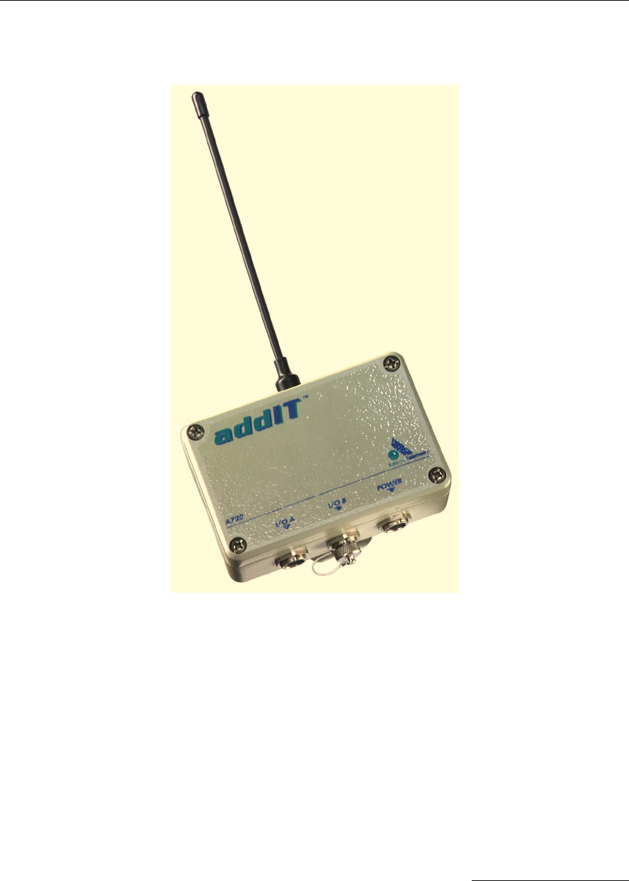
Wireless Sensor Interface A720 (addIT™)
1. About the A720
The A720 Wireless Sensor Interface (also known as
addIT™
) is a low power, short
range telemetry device, capable of sampling up to 6 analog sensors and 4 digital in-
puts (of which 2 counter types); in addition, it can control two relays.
The frequency of operation is in the 432 to 470 MHz range, making it adaptable to
most radio communication regulations in the world. The output power is under 10
mW, while the modulation is narrow band FM (12.5 or 25 kHz channel spacing).
Due to its construction, as well as to the software controlling it, the power consump-
tion is extremely low (average 6 mW). The unit operates from a built in NiCd 6.2 Volt
rechargeable battery, which is charged either using an 600mW solar panel or an ex-
ternal power supply adapter. A special configuration may be implemented where no
internal battery is used, rather the power is obtained exclusively over an external
connector.
The A720 is a ruggedized unit, complying with the IP65 environmental protection
class (NEMA 4). It can be easily installed and it integrates perfectly in an Adcon A730
system. Depending on the terrain, it assures a reliable wireless connection to an
A730MD or A730SD device to distances up to 800 meters, under favorable conditions
even more.
6
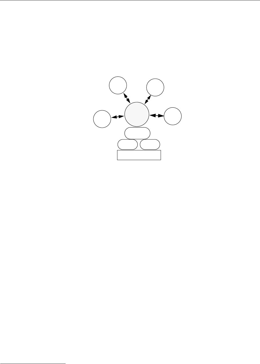
Wireless Sensor Interface A720 (addIT™)
2. Hardware
Most of the electronics are situated on the main board, while an interface board is
used to connect the unit to the outside world. The main board contains a radio unit,
a low speed modem interface, a microcontroller and a power management sub-
system.
For further details you may want to consult the schematic diagram located on page 7.
2.1. The Radio Unit
It consists of a RF transceiver, that conforms or surpasses the ETSI 300 220 specifica-
tions. The receiver is a double superheterodyne type, first oscillator being synthe-
sized. The transmitter is also synthesized, only the PLL chip and the frequency
reference being common (there are two separate VCOs, one for the receiver’s local
oscillator and another for the transmitter).
2.1.1. Receiver Section
The antenna signal is fed through a low pass filter and the antenna switch (D1/D2)
to a helical band-pass filter (it has a 20 MHz passband at 3dB), which attenuates the
first image and the oscillator fed-through signal. A cascode chip (U3) is used for RF
signal preamplification and first mixer, the LO being fed via the second emitter of the
cascode. The resulting IF on 45 MHz is filtered through XF1 which in this case pro-
vides the image attenuation for the second mixer.
After a pre-amplification by means of the transistor Q11, the 45 MHz IF signal is ap-
plied to U10, which provides the second frequency change to 455 kHz, pre-amplifi-
cation, limiting and FM demodulation. The second oscillator is also built into this
Radio Unit
Antenna
µController
Modem
Interface
Power
Management
System Supply
Battery
External Power
ADC
6
4
Analog Inputs
Digital I/O

8
Wireless Sensor Interface A720 (addIT™)
chip, a third-overtone quartz oscillator oscillating on 44.545 MHz. The 12.5/25 kHz
selectivity is obtained through the use of the two ceramic filters CF1 and CF2 (ver-
sion GX for 12.5 kHz or EX for 25 kHz channel spacing), exhibiting a low group delay
time. An interesting feature of U10 is its coilless demodulator, which is PLL based.
By adjusting R67 and R60 one can change the bandwidth and the central frequency
of the IF demodulator.
The data signal is obtained on pin 17 of U10 and is buffered by means of U8:D. In
addition to the data signal, an RSSI signal is obtained on the pin 18 of the same U10.
The signal is multiplexed with other DC signals (battery level and on-board temper-
ature) by means of U6 and U7 and then is presented to one of the A/D inputs of the
microcontroller.
The entire receiver section is enabled by the microcontroller through Q8.
2.1.2. Synthesizer Section
The synthesizer is based on a very low power PLL chip, U2. An important feature of
the chip is its FastLock™ mechanism, which improves the locking speed of the loop
without compromising on the VCO noise. The operation of the PLL chip is directed
by the microcontroller (operating frequency and channel step) and are therefore fully
under software control. The frequency reference is obtained from the highly stable
temperature compensated crystal oscillator OSC1.
There are two separated VCOs: one for the receiver section and a second for the
transmitter section. The receiver oscillator is 45 MHz higher than the transmitter os-
cillator, the latter being on the programmed operating frequency. This solution opti-
mizes the operating range of the individual VCOs, and keeps the noise level down.
The receiver VCO is realized with Q6 as oscillator and Q4 as buffer/amplifier, while
the transmitter VCO with the pair Q2/Q1. The configuration of the two VCOs is very
similar: in order to minimize the power consumption, the transistors are connected
in series from a DC perspective, the buffer being the load of the oscillator.
A small amount of RF from each VCO is fed to the PLL chip input (to the internal
prescaler) by means of the group C47/R27, and C16/R7 respectively. The output of
the PLL from the phase comparator/charge pump is filtered by means of the low
pass filter formed by C35/R29/C36/R22/C55 and applied to the two varicap diodes
D4 and D3. In addition, the FastLock mechanism occasionally activates R21 to in-
crease the current of the charge pump (you may want to consult National Semicon-
ductor’s Application Note AN-1000 “A Fast Locking Scheme for PLL Frequency
Synthesizers”, by D. Byrd, C. Davis, W.O. Keese, July 1995 for additional details on
the FastLock mechanism).

9
The Modem Interface
2.1.3. Transmitter Section
The transmitter section uses the VCO composed by Q2/Q1. This VCO is modulated
on the anode of its varicap diode (D3) by means of a small amount of the data signal.
Before modulation, the data signal is filtered by a four-pole low-pass filter built
around U1. The filter effectively removes the harmonics on the data signal in order
to keep the adjacent channel power under the required level.
The output of the VCO/buffer amplifier is applied to the power amplifier, operating
in class A thus minimizing the harmonics (Q3). The output of the amplifier is direct-
ed to the antenna through the antenna switch and the low pas filter. The antenna is
switched on transmit mode when a positive current is applied on the anode of D1 via
R12. The DC component is obtained from the collector of the power amplifier (Q3).
C11 is used to pass along the RF component.
The transmitter is activated by the microcontroller in two steps:
• The PLL is switched on (by means of Q5);
• After a delay of about 5 mS when the PLL has settled, the power amplifier is
switched on (by means of Q7).
The above mechanism assures a clean transmission start, avoiding that the transmit-
ter “spills-out” its carrier on several channels before stabilizing. The switch off fol-
lows the same principles, but in a reverse order.
2.2. The Modem Interface
The modem operates with two tones: 1 kHz (representing the 1 bits) and 2 kHz (rep-
resenting the 0 bits). A bit cell is represented by a complete time period (
1/f
), thus the
raw throughput varies between 1 and 2 kbps (average 1.5 kbps). The modem func-
tionality is essentially implemented in software. However, a signal conditioning is
performed on both receive and transmit paths.
On receive, the buffered analog data signal from U8:D is applied to a 3 kHz low pass
filter (U8:A). The filter output is further fed both to a Schmidt trigger (U8:C) and a 50
Hz low pass filter (U8:B), the output of the latter being used as a reference for the slic-
er (the Schmidt trigger). The TTL data,
RXDO
, is obtained at the output of the slicer
(i.e. on TP2). The microcontroller overtakes the decoding operation (see also “Mod-
ulation Technique Used” on page 43).
On transmit, only the low pass filter built around U1 is used: its role is to “smooth”
the square signal
TXDI
generated by the microcontroller.

10
Wireless Sensor Interface A720 (addIT™)
2.3. The Microcontroller and the Power Management Sections
The operation of the whole unit is under the control of U9, a PIC16C77L microcon-
troller. It is a powerful chip exhibiting an extreme low power consumption. Its main
jobs are:
• Controls the radio unit;
• Implements the modem functionality;
• Assembles the radio frames and waits for requests from a remote;
• Performs the sampling of the sensor inputs and the A/D conversion;
• Stores the values in a local FIFO; manages the FIFO;
• Implements the pulse counter function;
• Increments the Real-time clock;
• Assures the power management;
• Implements a serial Command Line Interface (CLI).
Note: For more details on some of these functions, see also the chapter “Software” on page 34.
The chip operates at its maximum speed, in this case 4 MHz (the “L” version) and
uses a crystal (X1). The real time clock is implemented by means of a 32.768 kHz crys-
tal (X3) connected on the internal TIMER1.
The radio unit is controlled via the SPI bus on one hand (to set the PLL chip param-
eters) and via the switches Q8 (for receive) and Q5/Q7 (transmit). As already men-
tioned, the modem is implemented in software: the output signal is available on RB1
(
TXDI
), while the receiver output is fed on the RB0/INT pin (
RXDO
).
The A/D subsystem is used to sample the inputs (AN0 to AN5); the 7th analog input
is used for on-board measurements (local battery, internal temperature and RSSI sig-
nal, switched by means of the analog switches U6 and U7); a stable 2.5 Volt reference
supplied by U4 is applied to the RA3/AN3/Vref pin. The reference is powered by
the microcontroller only when sampling the A/D inputs. The external sensors are
powered through U13.
The sampled input values are stored in a FIFO built with a serial EEPROM chip, U5.
These values may be retrieved when a pertinent request is received over radio, or
over the serial line. Additional configuration parameters are stored in the EEPROM,
e.g. the serial number of the device, the operating frequency, etc.
The pulse counter functionality is implemented by means of the two inputs RB6 and
RB7, based on the
interrupt on change
feature implemented in the PIC16C7x series of
microcontrollers.
The power management controls the charge/discharge of the battery (via Q9 and
U11), senses the misery levels and switches off the unit in order to protect the battery
(again U11). In addition, the software senses a storage condition, where no activities

11
The Interface Board
must be performed thus driving the unit in the hibernation mode. If the unit was
completely switched off due to an extremely low battery level, Q10 would start it up
again only if external power is applied to the power connector (e.g. from a solar pan-
el).
The terminal mode is implemented by means of the built-in UART. No on-board lev-
el drivers are present in order to minimize power consumption; a special adapter ca-
ble that performs the TTL to RS232 level shift and vice-versa is available. By means
of this cable and using the implemented commands, various parameters can be
changed/configured (see also the chapter “Software” on page 34).
2.4. The Interface Board
The interface board assures the connection between the main board described above
and the outside world. It contains the three connectors (
I/O A
,
I/O B
and
POWER
) and
some passive components protecting the pulse inputs. Each of the
I/O
connectors can
accept:
• Three analog inputs;
• One digital Input or Output (its functionality can be switched remotely);
• One pulse counter input.
The
POWER
connectors allows for:
• External supply (battery or any DC source from 5 to 10 volts);
• External charge supply (either a solar panel or an AC adaptor) if an internal
rechargeable battery is used;
• Communication over serial lines, at 19200 baud.
Note: The serial line is TTL compatible, a special adaptor cable must be used to reach the RS-232
levels. If an external battery is used, then the internal battery must be disconnected.

13
Programming the Boards
3.1. Programming the Boards
This section will be completed later.
3.2. Setting-up the Default Parameters
The tuning procedure is not possible without first configuring some default param-
eters on each unit. This is done using a special serial cable connected between the
A720MB with an A720CA interface to a PC; in addition, a communication terminal
program (e.g. Hyperterminal, in Microsoft® Windows™ 95) is needed to send the
commands. The terminal program must be configured as follows:
• 19200 Baud
• 1 Stop bit
• No parity
• No protocol (neither hardware, nor software)
To check that the communication is operational, press the
ENTER
key: an
OK
should
appear on the terminal screen. Using the
SET
command, following default parame-
ters must be pre-loaded (for more details on the meaning of the commands, consult
the section “The Terminal Task” on page 39):
SET OWNID 1
SET PMP 65 72
SET SLOT 900 3
SET RSSI 58
SET BL 432000000 450000000
SET FREQ 432000000 25000
The last two
SET
commands are valid for the units that will be trimmed for the low
band; for the high band, they must be replaced by:
SET BL 450000000 470000000
SET FREQ 450000000 25000
Note: The SET BL command sets the band limits, while SET FREQ sets the operating frequency;
before shipping and depending on the target country these two parameters may be changed.
The SET BL command must be issued always before the SET FREQ command.
3.3. Tuning
The tuning can be performed only after the units are programmed and the default
parameters are set, as described previously.
RxD
TxD
Ground
Battery
Ext Power
1
2
3
4
5
14
Wireless Sensor Interface A720 (addIT™)
3.3.1. Definitions
The diagram of the setup environment is depicted in
Figure 3.
Figure 2.
Trimming Setup.
The testing fixture is used to fasten the PCB under test both mechanically and elec-
trically in such a way to allow its rapid and comfortable trimming. It consists of a me-
chanical breadboard with two screws that are used to fasten the board; 5 elastic pins
are used to transport the relevant signals from the PCB to their corresponding appa-
ratus test cables. In addition, a switch (
Power/Sens. <–> Wobble
) allows switching of
the antenna input/output to the network analyzer or to the service monitor. The
schematic diagram of the testing fixture is depicted in
Figure 3.
Figure 3.
Schematic Diagram of the Testing Fixture.
0.765 V
Power/
Sens Wobble
Out
Scope
In/Out
Service
Monitor
In
Network
Analyzer
Out
Voltmeter
Out
Network
Analyzer
Testing
Fixture
RS232 To/From PC
+
–
6.5 V
A720MB
Connector
Optional
Scope Service Monitor Network Analyzer
Voltmeter
Scope
Service
Monitor
In Network
Analyzer
Out Network
Analyzer
Wobble
Power/Sens.
Ant
Gnd
TP4
A720MB
TP2
TP1 Voltmeter
680 W
12 KW
1 MW

15
Tuning
There are only three tuning elements to be acted upon: FL3, L6 and L10. Their loca-
tion on the PCB (all upper side) is depicted in the schematic below:
3.3.2. Test Equipment Settings
Before proceeding, certain controls on the test equipment must be set; some of the
settings depend of the operating band (high or low) of the device under test (DUT).
In addition, it is highly recommended that the ambient temperature during trim-
ming is 24° C (±2°C).
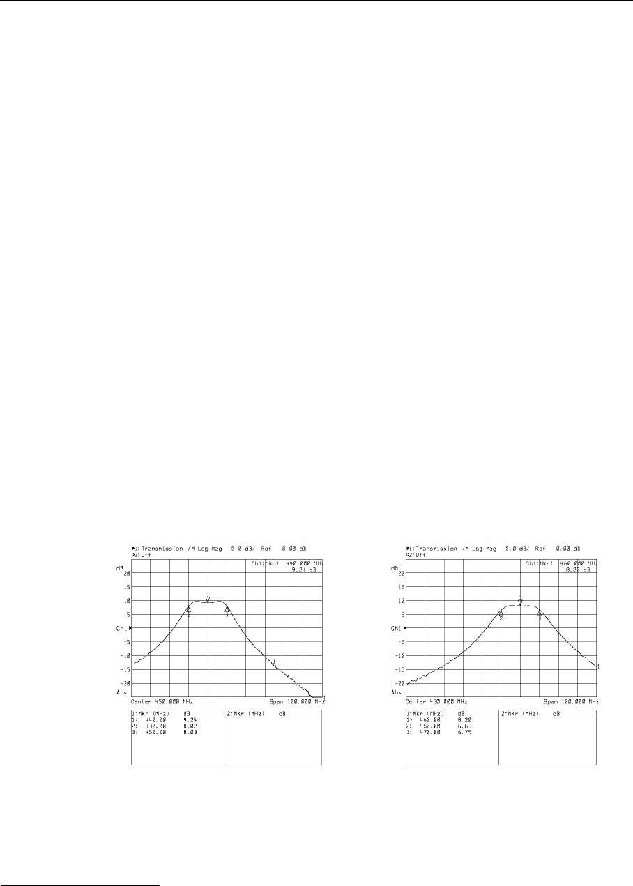
3.3.2.1. Network Analyzer (HP 8711)
The settings for the Network Analyzer are as follows:
• Center frequency: 450 MHz
• Span: 100 MHz
• Display: 5.0 dB/div
• Power: -20 dBm
• Markers:
— low band Mkr1 – 440 MHz, Mkr2 – 430 MHz, Mkr3 – 450 MHz;
— high band Mkr1 – 460 MHz, Mkr2 – 450 MHz, Mkr3 – 470 MHz.
Note: A good idea is to store the instrument state for the two settings, low band and high band.
3.3.2.2. Service Monitor (Rohde & Schwarz CMS50)
The setting for the receiver section check are as follows (RX-TEST):
• SET RF: 432000000 Hz (Low band) / 450000000 Hz (High Band);
• RF LEV: 5 µV (see also note below);
• SINAD;
• AF1: 2kHz;
• MOD1: 3.5 kHz;
• SCOPE MODE;
• BEST RANGE.
FL3
L10
L6
16
Wireless Sensor Interface A720 (addIT™)
The settings for the transmitter section check (TX-TEST):
• COUNT: (should show the transmitter carrier frequency);
• POWER: (should show the transmitter carrier power).
Note: If using the Testing Fixture, a calibration should be performed to check the losses in the an-
tenna switch, cables, etc. Depending on these losses (which at 450 MHz can amount up to 6
dB), it may be needed to adjust the RF LEV value accordingly (up to 10 µV). Similarly, the
measured output power must be correspondingly downgraded (see also “Checking the Trans-
mitter Parameters” on page 18).
3.3.3. Adjusting the Receiver Front End
• Mount the DUT on the testing fixture and connect it to the PC via the serial
cable;
• Select the appropriate instrument profile depending on the device’s band
(High or Low);
• Turn on the receive subsystem of the DUT by entering the
RX
command at the
terminal;
• Check that the switch on the Testing Fixture is in the
Wobble
position;
• Adjust the filter FL3 until you obtain a curve similar with one of those shown
in
Figure 4.
(depending on the band); this is done by successively adjusting the
two trimming screws located on the filter.
If this is not possible, check the power supply, the cable connections to/from the test
equipment, etc. In addition, verify if you have approx. 1.1 volts on the test point TP4.
Finally, check if all 8 pins of the filter FL3 are properly soldered.
Figure 4.
Helical filter’s diagrams for Low Band and High Band devices.
Low Band High Band

17
Tuning
3.3.4. Adjusting the VCOs
• Flip the switch on the Testing Fixture to the
Power/Sens.
position;
• Be sure that the DUT is in receive mode (enter the
RX
command at the terminal
program);
• Adjust the coil L10 until the voltage shown on the digital voltmeter is 700 mV,
±50 mV (see also the note below);
• Switch the unit in transmit mode, by entering
XMIT
at the terminal;
• Adjust now the coil L6 until the voltage shown on the voltmeter is again
700 mV, ±50 mV;
• Press the enter key at the terminal to switch the unit off.
Note: If using the Testing Fixture, a calibration may be needed, due to internal resistance of the
Voltmeter and the serial resistor mounted on the Testing Fixture. The calibration is performed
by measuring the VCO voltage directly on the TP1 and by comparing the value with that
measured through the Testing Fixture. The values given above are the real ones, measured di-
rectly.
If the above limits cannot be attained, or the readout is very unstable, check the fol-
lowing:
• If the programmed operating frequency is 432 (Low Band) and 450 MHz
(High band) respectively. To check this, type at the terminal prompt the com-
mand
FREQ
, the device will answer returning this parameter;
• If the respective commands (
RX
and
XMIT
) were issued;
• If some parts are not missing, have the incorrect value, or badly soldered
(check the parts around Q2 and Q6).
3.3.5. Checking the Receiver Parameters
• Check that the switch on the Testing Fixture is flipped to the
Power/Sens.
po-
sition;
• Switch the DUT to receive mode by typing at the terminal the command
RX
;
• Switch the Service Monitor to RX TEST mode, on the appropriate frequency
(432 MHz for low band and 450 MHz for high band); the level should be 5 µV
(see also “Test Equipment Settings” on page 15);
• The S/N ratio should be at least 10 dB; in addition, if a ‘scope is also connected
a clear 2 kHz sine wave should be visible, with a relatively low amount of
noise superimposed;
• Switch the DUT in pulsed mode (press the enter key);
• After several seconds, you will see the image on the ‘scope pulsing at about
one second intervals;
• Switch the RF generator output off;

18
Wireless Sensor Interface A720 (addIT™)
• Check if the RSSI threshold is correct: type the command
RSSI
– the actual val-
ue must be lower than the threshold set. If this is not the case, repeat several
time the
RSSI
command, maybe a transmission just happens (a radio scanner
set on the operating frequency would help detect foreign transmissions). If the
threshold difference is marginal, then you must increase it by using the
SET
RSSI
command (it must be 20 to 30% higher than the actual value).
If the any of the above targets is not reachable, check first visually if the chip U10 is
correctly soldered and that no shorts exist between its pins (most problems usually
appear around this chip). If the S/N ratio test is positive but the last check is not, then
check U8 and the components around it.
3.3.6. Checking the Transmitter Parameters
• Check that the switch on the Testing Fixture is flipped to the
Power/Sens.
po-
sition;
• Switch the DUT to transmit mode by typing at the terminal the command
XMIT 0
;
• Switch the Service Monitor to TX TEST mode, on the appropriate frequency
(432 MHz for low band and 450 MHz for high band);
• You should see the following parameters on the Service Monitor readout:
1. Carrier: 432000000, respectively 450000000 Hz (± 500 Hz);
2. Output Power: 9 dBm (+1dBm, -2dBm);
3. Frequency Deviation: ±2.3 kHz (±0.2 kHz) for 12.5 kHz units and ±4.0 kHz
(±0.5 kHz) for 25 kHz units;
• Switch the unit in stand-by (press the enter key).
If item 1 above cannot be achieved, replace R36 with a 12 K
W
resistor to shift the fre-
quency up, or R35 with a 10 k
W
resistor to shift the frequency down. If item 2 cannot
be achieved, check the solder and components around Q1 and Q3; in addition, check
if D1 and D2 are the right components (sometimes they are replaced by other visu-
ally similar parts). Finally, if item 3 cannot be achieved, replace R17 with a lower re-
sistor to reduce the deviation, or a higher one to increase it. Note that depending on
the device type, R17 can be either 470
W
(12.5 kHz) or 1 k
W
(25 kHz). If no modulation
is present at all, then check U1 and the parts around it.
3.3.7. Data Transfer Check
The last check is a radio data transfer. In order to perform it, at least a base station
(model A730SD) or a normal remote station (model A730MD) should be installed
and operated on the same test frequency (either 432 or 450 MHz), in the near vicinity
(no more than 30 m).
Note: The base or remote station used for this test must be operated with a fictive antenna (a 50
W
resistor).

19
Additional Issues Related to Type Approval Testing
The test is performed by entering at the terminal prompt the command
B
: the base
and/or remote station must answer with the RF in and out values. If no answer is
received after several seconds, then retry the command. If still no answer is received,
then check with a scope on TP2 if the digital data is present (on receive); if not avail-
able, check U8:C and the parts around it. In addition, a radio receiver tuned on the
operating frequency can also supply a rough indication whether the receiver or the
transmitter are defective.
3.4. Additional Issues Related to Type Approval Testing
This chapter is intended for the bodies (laboratories) performing the tests required
to obtain a Test Report.
3.4.1. Controlling the Unit
The unit under test can be controlled by means of the special serial cable supplied by
Adcon Telemetry connected to a PC (e.g. a laptop) on one side and the
POWER
con-
nector of the unit on the other side. In order to switch the unit in various modes of
operations, a simple communications terminal program will suffice (e.g. Terminal or
Hyperterminal in Windows, or Kermit under other platforms). The most important
commands used are
XMIT
,
RX
and
SET FREQ
. For a list of all supported commands and
the parameters they expect, see also “Supported Commands” on page 39. For addi-
tional details on how to configure your terminal program, see “Setting-up the De-
fault Parameters” on page 13.
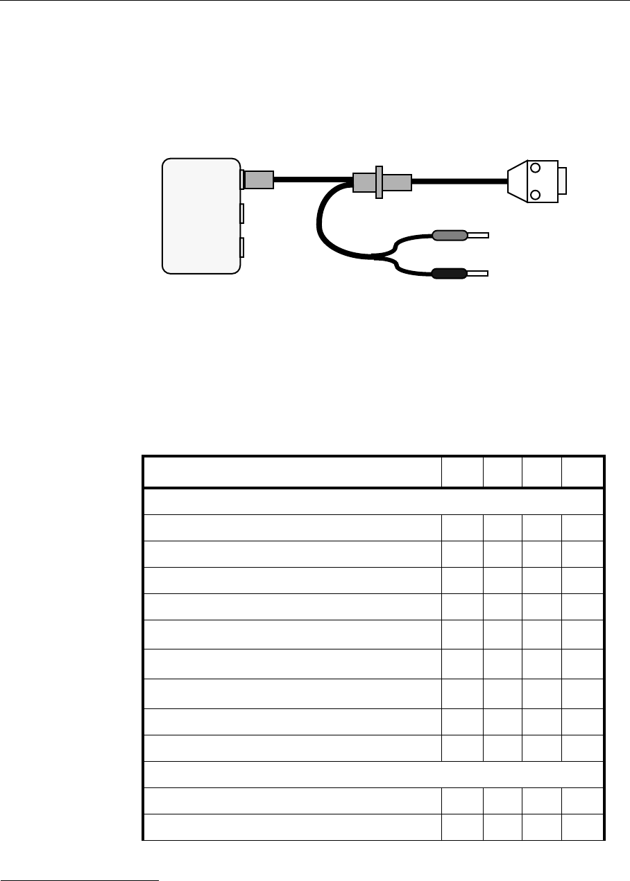
3.4.2. External Power Supply
In order to test the unit over the specified supply range, a special power cable is sup-
plied by Adcon Telemetry. This cable must be connected to the
POWER connector of
the unit before the serial cable. The two wires with banana plugs can then be connect-
ed to an external variable power supply: the red plug to plus and the black one to
minus. However, before doing this, the internal battery must be disconnected. Here
is how:
• Open the lid by unscrewing the four screws in the corners of the addIT box;
• Gently remove the lid (the battery is fixed on the lid and is connected to the
electronics board by means of two wires);
• Remove the battery’s plug from the PCB connector;
• Mount the lid back, taking care that the rubber gasket sealing the box is not
out of its place;
• Screw the four screws back, applying a moderate force.
Note: If the rubber gasket is not properly mounted, the unit loses its IP65 environmental protection.
In addition, certain radiated limits cannot be guaranteed.
20
Wireless Sensor Interface A720 (addIT™)
WARNING! Do not apply more than 10 Volts to the unit: permanent damage of the de-
vice may result. Note also, that the internal microcontroller will switch off the unit
when the battery voltage drops below 5.5 Volts, and under 5.9 Volts the RF opera-
tions may be stopped.
Figure 5. Connection of an external power supply.
3.4.3. Specifications
The A720 was intended to fulfill the specification of the ETSI 300 220, Class I, Sub-
classes a and b, but other national norms are similar to this (e.g. the CFR 47, Part 90,
Subpart J). Following are the main operational parameters of the A720:
Parameter Min Typ Max Unit
Common
Supply 5.0 6.2 10.0 V
Operating Temperature -30 +70 °C
Relative Humidity 10 99 %
Class Protection IP65
Data Rate (Using the On-board Software Modem) 1000 150a2000 bps
Operating Frequency (Low Band version)b432 450 MHz
Operating Frequency (High Band version)b450 470 MHz
Frequency Stability (-20 to + 60 °C) ±1.5 kHz
Frequency Stability (-30 to + 70 °C) ±2.5 kHz
Receiver
Sensitivity (10 db S/N) -93 dBm
Image Frequency Attenuation (1st IF = 45 MHz) 70 dB
POWER
I/O A
I/O B
+
-
Black
Red
5 to 10 Volt
RS232
+
+
Power Cable Serial Adapter Cable

21
Additional Issues Related to Type Approval Testing
Local Oscillator Leakage 2 nW
Adjacent Channel Attenuation (both versions) 70 dB
RSSI dynamic 90 dB
Operating Current (incl. On-board Microcontroller) 15 mA
Transmitter (all measurements made on a 50 W resistive load)
Output Power 7 9 10 dBm
Spurious Radiation (0 to 862 MHz) 2 nW
Spurious Radiation (862 MHz to 3.5 GHz) 200 nW
Adjacent Channel Power (12.5 kHz version) -32 dBm
Adjacent Channel Power (25 kHz version) -44 dBm
Occupied Bandwidth (12.5 kHz version) 8.5 kHz
Occupied Bandwidth (25 kHz version) 15 kHz
Operating Current (incl. On-board Microcontroller) 50 mA
a. Data rate is content dependent.
b. This parameter represents the tunning range; the switching range can be
software limited to a narrower space (even to the extent of a single channel).
Parameter Min Typ Max Unit
22
Wireless Sensor Interface A720 (addIT™)
Several graphs obtained by means of a Rohde & Schwarz Spectrum Analyzer (model
FSEA) are attached, reflecting some of the measured parameters.
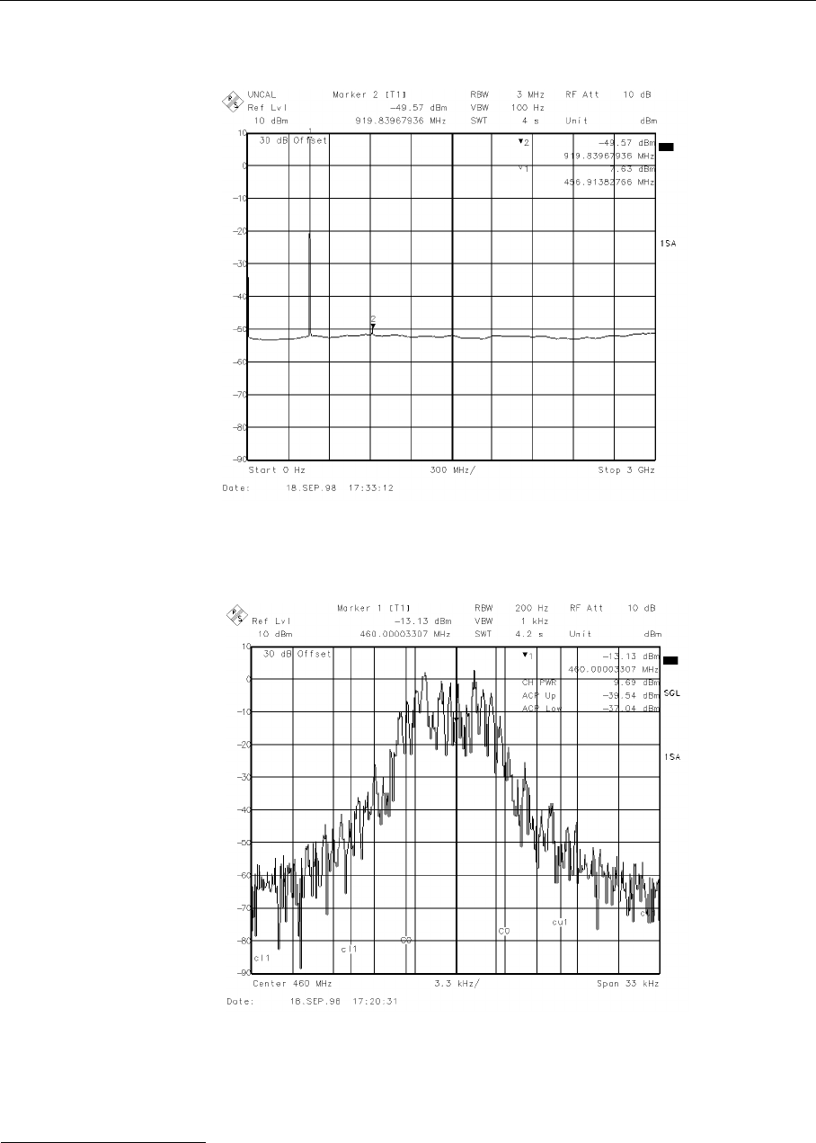
Figure 6. Spurious radiations (Marker 2); except the second harmonic, no other overtones
are visible.
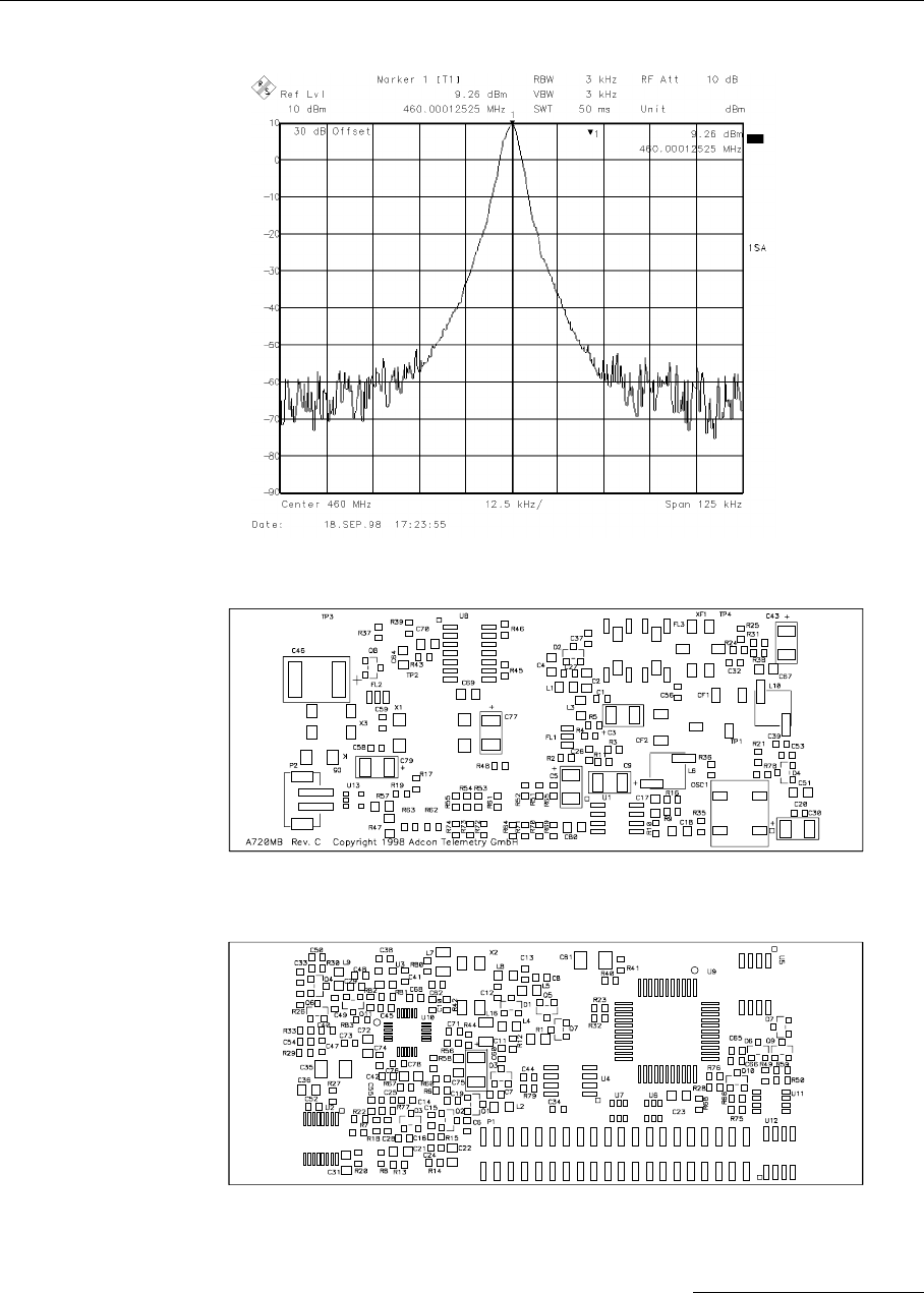
Figure 7. Adjacent Channel Power, 460 MHz, 12.5 kHz version, modulated with a 0x55
tone (1500 bps).
23
Additional Issues Related to Type Approval Testing
Figure 8. Spectral purity: an unmodulated carrier at 460 MHz is shown.
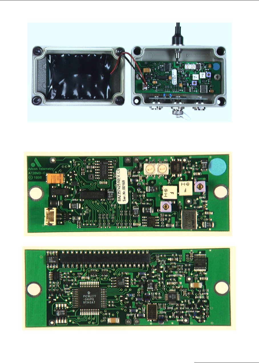
Figure 9. The TOP side of the printed circuit board.
Figure 10. The BOTTOM side of the printed circuit board.
28
Wireless Sensor Interface A720 (addIT™)
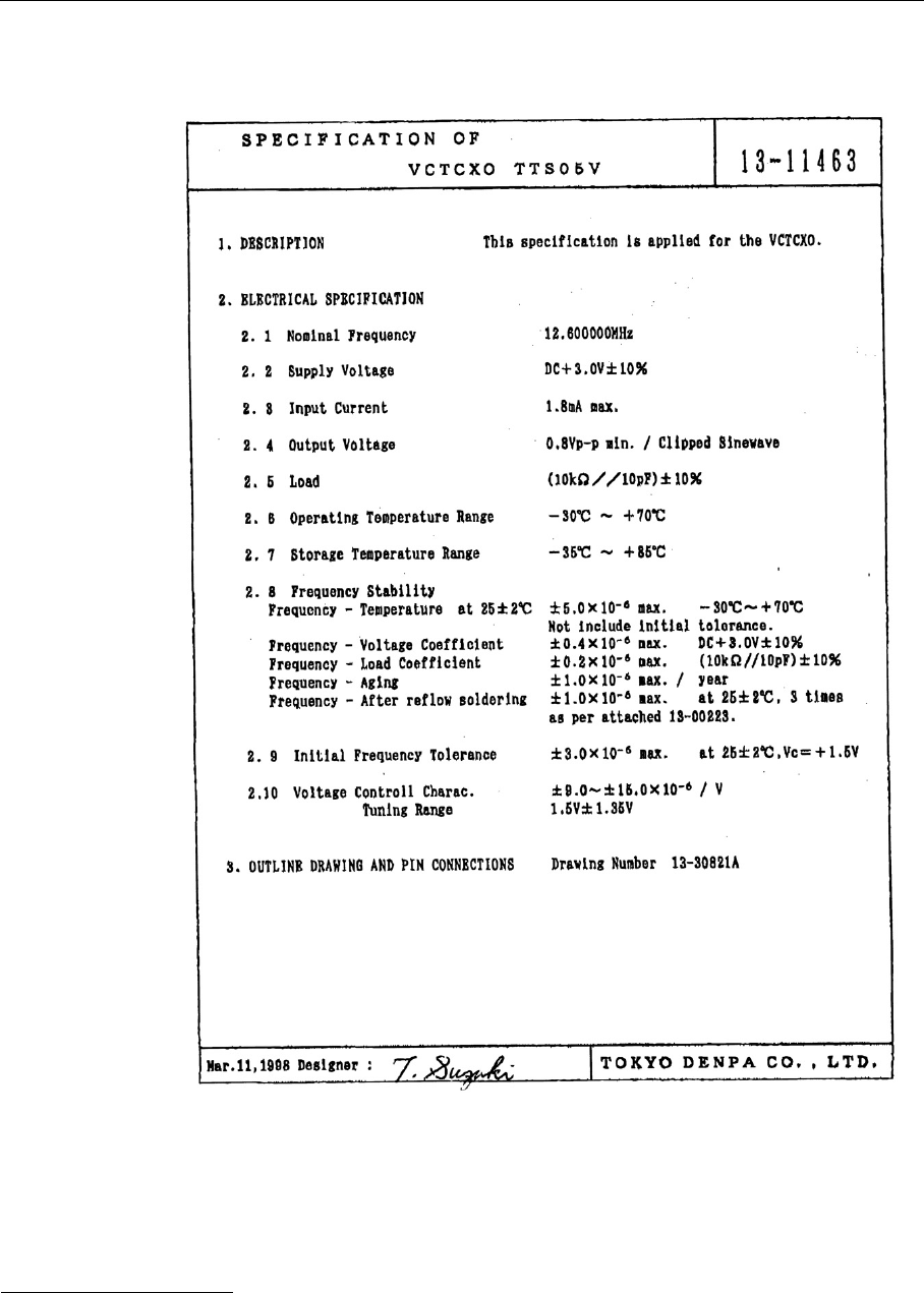
Figure 11. The VCTCXO Specification. This part is used as frequency reference for the PLL
synthesizer.
29
Additional Issues Related to Type Approval Testing
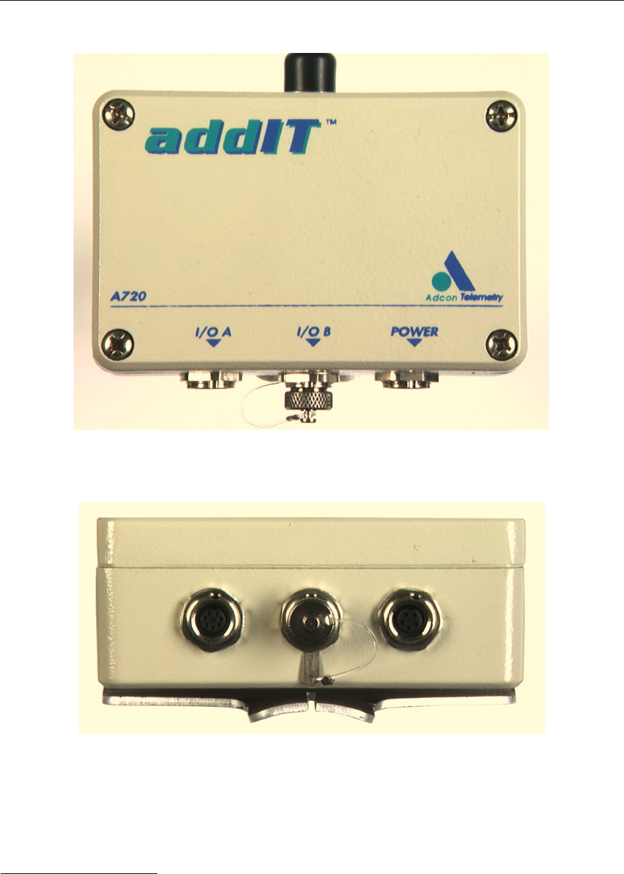
3.4.5. Device Photographs
Figure 12. General view.
30
Wireless Sensor Interface A720 (addIT™)
Figure 13. Front view.
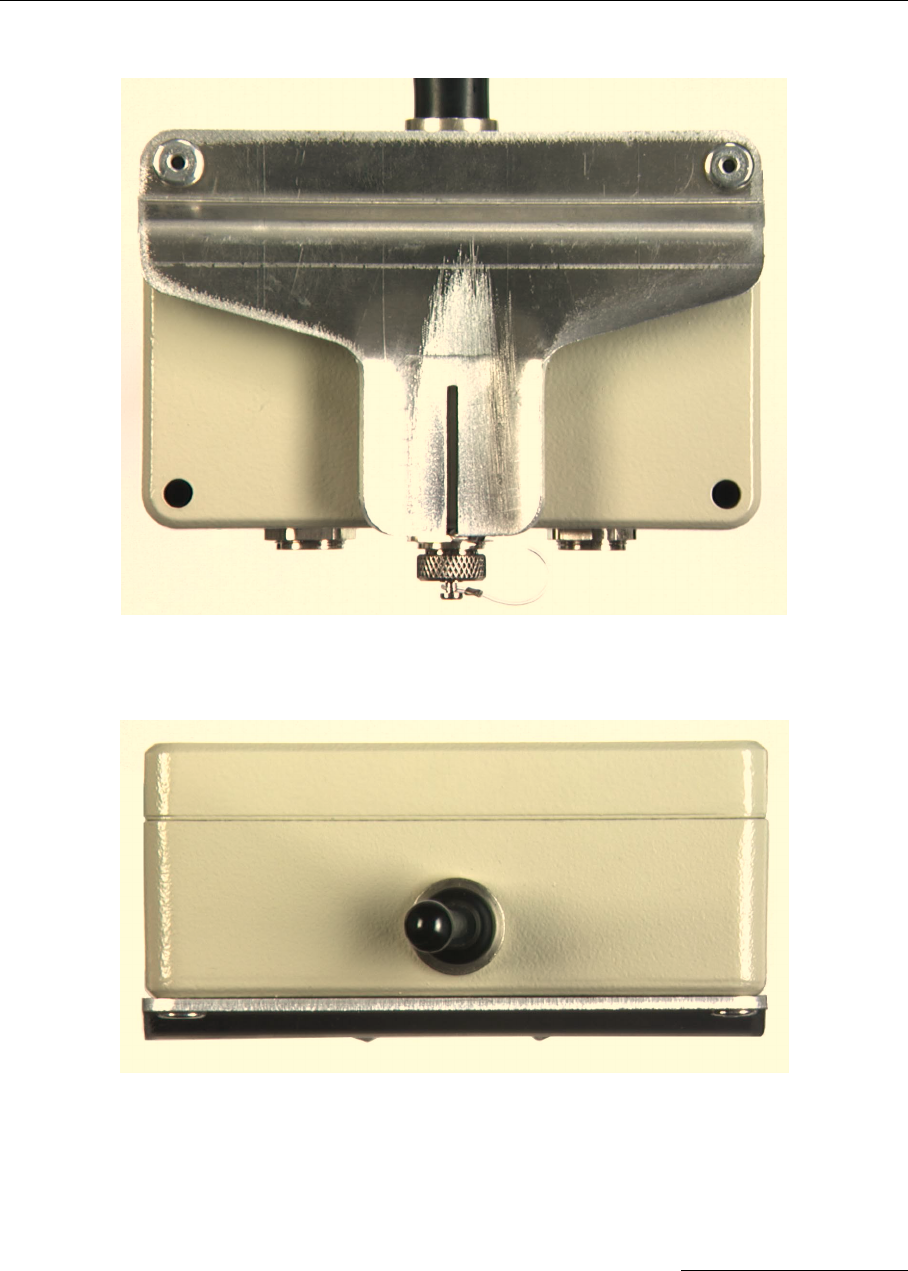
Figure 14. Bottom view.
31
Additional Issues Related to Type Approval Testing
Figure 15. Back view.
Figure 16. Top view.
32
Wireless Sensor Interface A720 (addIT™)
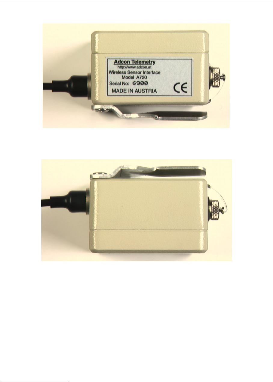
Figure 17. Left view.
Figure 18. Right view.
33
Additional Issues Related to Type Approval Testing
Figure 19. The A720 Opened.
Figure 20. The PCB.
TOP
BOTTOM
34
Wireless Sensor Interface A720 (addIT™)
4. Software
The software is written entirely in C. It consists of a collection of standard C library
functions, a minimalistic operating system (AMOS – Adcon Minimal Operating Sys-
tem) offering basic configuration and administration functions (including a com-
mand line terminal on a serial port), and the application software itself which assures
the desired functionality of the device.
Figure 21. General structure of the A720 software.
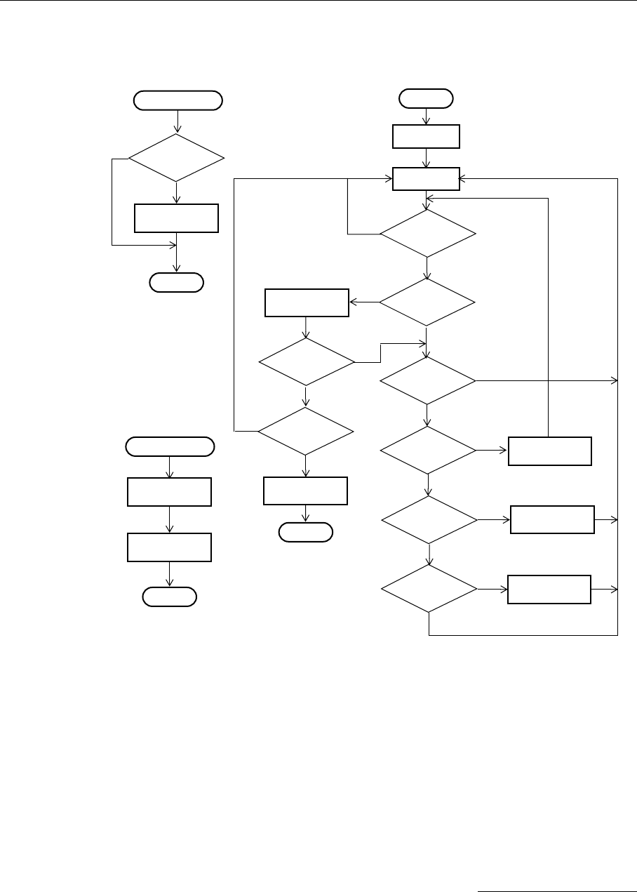
4.1. AMOS
Most of its time, the system is in sleep mode. Each 0.5 seconds, an interrupt is gener-
ated by the local 32.76 Khz crystal based real time clock (RTC). AMOS will check
what tasks need attention (i.e. must be executed) and pass them the control accord-
ingly. After all the tasks have finished their jobs, AMOS brings the system back to
sleep. The 0.5 seconds interrupt routine is used to increment the RTC.
In parallel to the normal, regular operation of the AMOS, the system responds to the
pulse counter interrupts (they are generated by two inputs on the microcontroller
and are used for event counting, e.g. rain gauges). These interrupts are handled by a
separate routine.
One of the main concerns of the software design is the power consumption of the de-
vice. The software must assure that all the peripherals are left in the correct state in
AMOS
Hardware
Device
Drivers
Device
Drivers
Standard
C Library
Task 1
Task 2 Task 3
Task 4
35
AMOS
order to reduce their consumption to a minimum; all operations are executed in the
shortest possible time.
Figure 22. General flow chart of the AMOS.
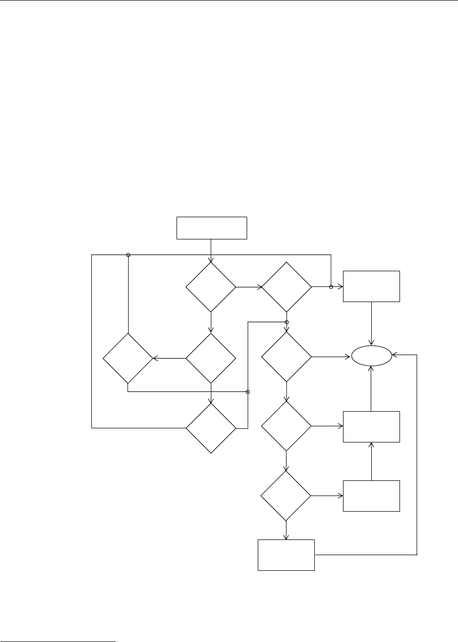
4.1.1. Initialization
This section initializes the peripherals needing an one time configuration, like:
• Microcontroller option registers;
• The RTC timer (Timer 1), in order to generate the 0.5 sec RTC interrupts;
• Various peripherals (SCI, Timers, A/D Converter, parallel ports).
Reset
Initialization
Sleep
0.5 sec
interrupt?
No
Yes
Connectivity
Check?
Do Connectivity
Check
Yes
Terminal
Mode?
No
Enable Terminal
Mode
Yes
No
RF Channel
Activity?
Handle Incoming
Message
Yes
No
Time to A/D
Sample?
A/D Sample
and Process
Yes
Switch off
Everything
Battery
Low? Storage
Mode?
Yes
No
No
No
Stop
Battery
Distress?
Yes
Yes
No
0.5 sec Interrupt
Advance the
RTC one second
Return
Increment
the RTC?
Yes
No
Counter Interrupt
Debounce input
Return
Increment
affected Counter
36
Wireless Sensor Interface A720 (addIT™)
4.1.2. 1/2 Second Interrupt
The interrupt handler will only increment the RTC, when needed (every other inter-
rupt); no other tasks are performed on this interrupt level. The interrupt is generated
by TIMER1 of the microcontroller.
4.1.3. Pulse Counters Interrupt
Interrupts are generated by two pins on the PORTB, having the Interrupt on Change
feature. The interrupt handler must store the previous state of the port, to act only on
a certain level (user programmable, by default is zero). Additionally, a debouncing
mechanism is implemented, allowing for different types of pulses to be counted. By
default, the filter is set at 1 ms (user configurable).
Figure 23. Flow chart of the Pulse Counters Interrupt handlers.
Note: The commands to configure the level and filter values must be documented; they are not yet
implemented in the current version.
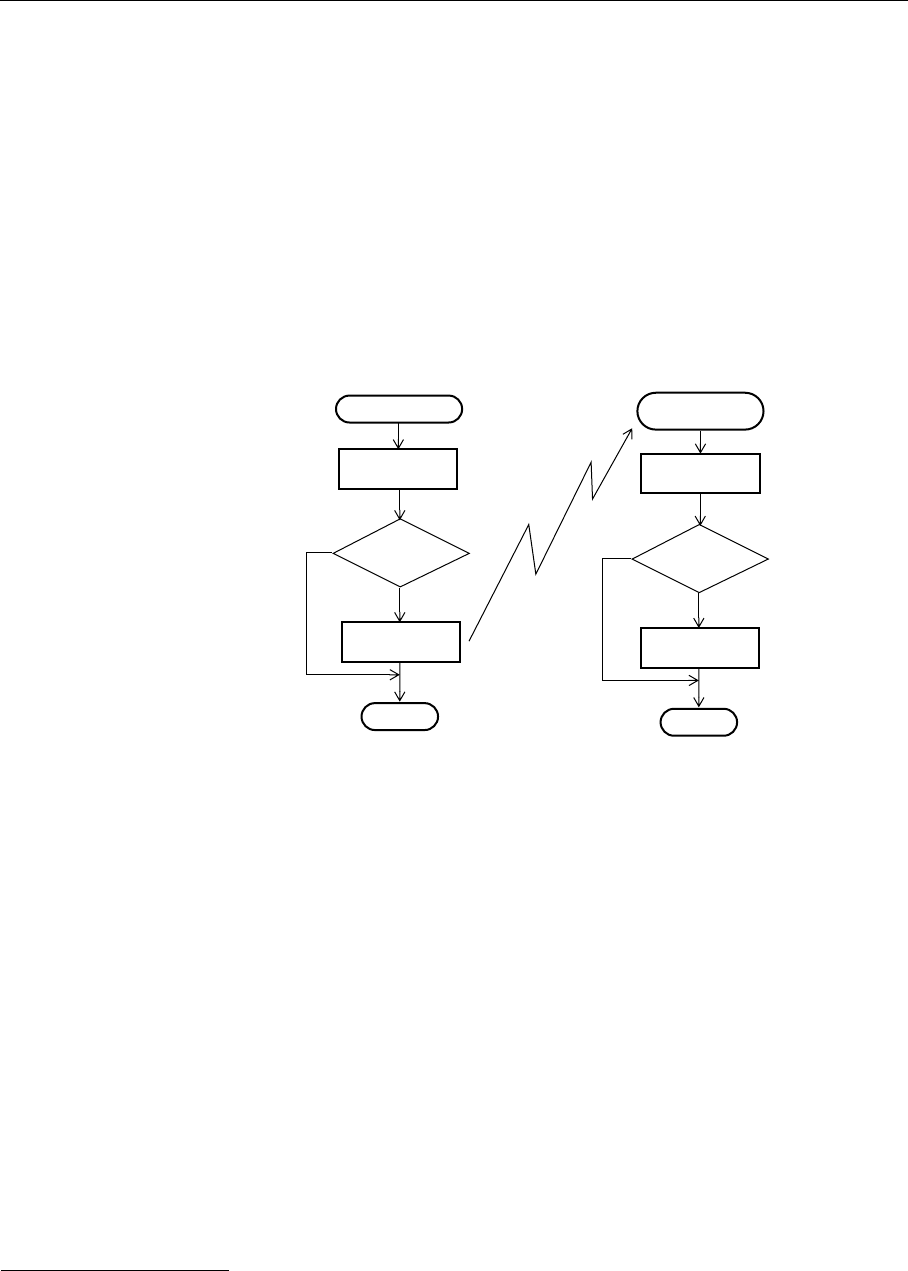
4.2. Mode Check
The system has the ability to check two input ports to switch itself in one of four op-
erating modes:
•Storage mode: in this mode, the unit is in a stand-by state, possibly stored in a
warehouse. The power supply is reduced to a minimum, by switching off al-
most all the functions of the device: the radio interface, the A/D sampling and
storage (only the battery will be monitored), and the pulse counter interrupts
will be disabled. To further reduce the power consumption, the 0.5 second in-
terrupt is switched to 2 second. However, the software accounts for this
change and the internal RTC will be correctly maintained.
Counter Interrupt
Return
Read
Port Input
Right
Level?
Yes
Arm
Debounce Timer
No
Debounce Timer
Interrupt
Read
Port Input
Return
Right
Level?
Yes
Increment
Counter
No
37
Mode Check
•Terminal mode: the device notices that a serial cable is connected to its POWER
connector, and is ready to accept commands. In this mode, all the subsystems
are enabled (A/D, pulse counters, radio interface, etc.), and the complete
functionality of the device is available.
•Connectivity check mode: in this mode, a special tool is plugged in the POWER
connector, in order for a user to check if the device is able to contact other de-
vices (normally an A730MD or an A730SD). The tool has a LED that will be
pulsed in several modes, depending on the results of the connectivity check
operation. After the operation is finished, the device will enter automatically
the normal operating mode (see next paragraph).
•Normal operating mode: this is the mode where the device polls every 0.5 sec-
onds the RF channel and waits for requests from a master (an A730MD or an
A730SD). In addition, it samples the analog and digital inputs every 5 minutes
and stores the averaged values in the EEPROM FIFO every 15 minutes. The
pulse counters are operated normally.
Figure 24. Flow chart of the Mode Check procedure.
0.5 Sec Interrupt
Return
Terminal mode
SCI
mode?
Yes
No
Yes
PD7 = 1?
PD6 = Out; PD6 = 1
PD7 = In
Enable SCI
No Storage mode;
Return
PD6 = 0
Yes
PD7 = 1?
Framing error?
No
Yes
Disable SCI
Set STORAGE
STORAGE Set?
No
Return
Normal mode
No
Yes Do connectivity test;
Reset STORAGE
Return
38
Wireless Sensor Interface A720 (addIT™)
More details on the functionality of each mode will be described when dealing with
the individual tasks.
4.3. A/D Task
This task is responsible for the actual sampling of the A/D inputs (where the sensors
are connected). In addition, the task is responsible for the power management of the
system: it checks the battery level and performs the following actions:
• Switches on and off the solar panel (that charges the battery), depending on
the battery state and internal temperature of the device;
• Brings the system in a low consumption mode if the battery is low;
• Switches the system off if the battery is in a misery state, in order to protect it.
Figure 25. Power Management flow chart.
Measure Battery
and Temperature
Temp
> 20°C?
Yes Batt
> 7.0 V? Switch Off
Yes
No No
Temp
< -10°C?
No
No
Yes
Yes
Batt
> 7.6 V?
No
Batt
> 7.3 V?
Batt
< 6.5 V?
Yes
Batt
< 5.5 V?
Yes
Exit
No
Switch On
No
Enter
Misery Mode
Batt
< 5.0 V?
No
Yes
Yes
Switch
Device Off
Note: The thresholds shown are
for reference only; actually
they are computed based
on the SET PMP command.

39
The Terminal Task
The A/D task is not executed at each 0.5 seconds interval, but rather every 5 minutes
(default). This parameter can be user configured (it is stored in the EEPROM section).
After the sensors inputs are sampled their values are averaged and stored as a slot in
the EEPROM FIFO buffer, time stamped. The number of samples is by default 3, but
is user configurable (this parameter is stored in the EEPROM section). These param-
eters are defined and can be changed by the SET SLOT command (see also “Supported
Commands” on page 39).
A special method of averaging is used in order to deal with various sorts of sampled
values (e.g. wind direction). In addition, the pulse counters are stored in the EE-
PROM with the slot and cleared afterwards.
4.4. The Terminal Task
The terminal offers a minimum of commands needed to configure and administer
the device, like setting and reading parameters (time, frequency, sampling rate, etc.),
checking the radio subsystem (switch it in various modes – receive, transmit, etc.).
The device enters in terminal mode whenever the mode checking routine senses that
a serial cable is inserted in the POWER connector. Periodically, it checks for that con-
dition, in order to automatically exit this mode (see also “Mode Check” on page 36).
In the inset are depicted the connection pins on the POWER connector, where the se-
rial cable is plugged.
Note: The interface is TTL, not RS-232! An adapter cable provided by Adcon must be used.
4.4.1. Supported Commands
Following is a list of available commands and an explanation of their use (the com-
mands are listed in upper case, but you can use lower case too, the device is not case
sensitive).
4.4.1.1. The SET Series of Commands
•SET OWNID nnnn – where nnnn is the Id number of the unit. The Id number
must be identical to the one written on the unit’s label.
•SET PMP bl bh – set the power management parameters. bl is the lower battery
level (the threshold where the charging of the battery will be switched on) and
bh is the higher battery level (the charging will be switched off). Both bl and bh
are expressed in volts x 10 (e.g. 72 means actually 7.2 V). Default values (fac-
tory programmed) are 65 and 72, meaning 6.5 and 7.2 volts respectively. Ex-
ample:
— if you want to change the switch on threshold to 6.3 and the switch off
threshold to 7.0 volts, issue the command SET PMP 63 70.
•SET SLOT storage samples – configures the input sampling and storing inter-
vals: storage represents the time (in seconds) elapsed between two slots stored
in the internal memory, while samples represents the numbers of samples used

40
Wireless Sensor Interface A720 (addIT™)
to build the average that will be stored. The default storage is 900 (15 minutes)
and samples is 3 (3 samples per quarter of an hour). Example:
— if you want to sample the inputs (sensors) every minute and build an hour-
ly average, issue the command SET SLOT 3600 60.
— if you want to sample the inputs once per hour and store the values as they
are, then the command SET SLOT 3600 1 will do the job.
In order to better understand the importance the samples parameter has, a table is
provided showing addIT’s expected operation time on a fully charged battery and a
50 mA total consumption for the sensors:
Note: Radio activity refers to the fact that one base station and between one and three A730MD sta-
tions/addITs are active on the same operating frequency as the addIT under test.
•SET BL ll ul – sets band limits; ll is the minimum allowable frequency, while ul
is the maximum allowable frequency. This command effectively limits the us-
er’s possibility to change the device’s operating frequency and it can be used
to fulfill specific requirements existing in certain countries. Example:
— if the law in a country limits the operation of the device between 433.150
and 434.750 MHz, then the command is SET BL 433150000 434750000.
— if the users are not allowed to change the frequency at all, then use the same
frequency for both ll and ul: SET BL 433925000 433925000.
Note: The SET BL command is not documented in the user manual.
•SET FREQ freq step – sets the unit’s operating frequency; freq is the frequency
and step is the channel spacing (both expressed in Herz). Example:
— suppose you want to change the frequency of an addIT to 467.1125 MHz
with a channel spacing of 12.5 kHz. After converting all the values to Hz, the
command to be used is SET FREQ 467112500 12500.
Note: The SET FREQ command may return an error if trying to program a frequency outside the
band limits; see SET BL command.
•SET RSSI value – set the Relative Signal Strength Indicator threshold. The facto-
ry default is set to 58 units. The RSSI threshold is used to detect if there is any
radio activity on the channel. The value set must be approximately 30% higher
than the actual measured value when no signal is present on the channel. To
measure the actual value use the command RSSI (explained later in this chap-
ter). Example:
— to set the RSSI threshold to 55, use the command SET RSSI 55.
Radio activity Sensor sampling
(samples/15 min) Average
consumption (µA) Estimated
operation (days)
No No sensors 450 92
Yes No sensors 540 77
Yes 1 750 55
Yes 3 (default) 1080 38
Yes 5 1450 28
Yes 15 3100 13

41
The Radio Interface Task
Note: The values of RSSI have no units, they are arbitrary; however, a value of 85 corresponds more
or less to the maximum value in addVANTAGE, i.e. 8 µV.
4.4.1.2. Querying the Actual Configuration Parameters
You can query an addIT to find out its actual configuration parameters. Typing OWN-
ID, for instance will return the actual ID an addIT answers to (it should be the same
as the one on its label). In addition to OWNID, PMP, SLOT, BL, FREQ and RSSI, the com-
mand VER will return the current software version of the device.
The RSSI commands returns two values: the actual measured value of the RSSI and
the value set as threshold. As noted elsewhere, the threshold must be approximately
30% higher than the actual measured value. The actual RSSI is unstable due to the
channel’s random noise, receiver’s internal noise, and/or to transmissions just tak-
ing place. If the actual RSSI value is consistently higher than the programmed value,
something must be wrong, or the channel is very noisy (however, before re-adjusting
the RSSI threshold, check this with a handheld radio receiver or a scanner).
Other commands available in terminal mode are:
•DUMP addr – displays 256 bytes of the internal EEPROM memory, starting
with the address addr (specified as hex values). Valid addresses for the model
A720 are B600 to B9FF. The last 16 slots of data (for 15 minutes slots, that
makes 4 hours of data) are stored at B900 to B9FF. The remainder are used for
internal configuration parameters or reserved for future use.
•RX – switches the device to receive mode until a key is pressed. This command
is used for trimming or checking purposes.
•XMIT param – switches the device to transmit mode until a key is pressed;
param may be 0 – a 2 kHz tone will be modulated on the transmitted carrier, 1
– a 1 kHz tone will be modulated on the transmitted carrier, T – a mixture of
1 and 2 kHz test tones, or missing – an unmodulated carrier will be transmit-
ted. This command is used for trimming or checking purposes.
•B – sends a broadcast frame and displays all the answers, with the RF levels
recorded for each received station.
4.5. The Radio Interface Task
The A720 is intended only as an end device in a radio network. Following frames are
recognized and serviced by an A720:
•PING – used to check if a device is alive; returns a PONG frame;
•REQUEST – returns a reduced data frame (DATA);
•RSETIO – switches the digital outputs and returns the digital inputs value;
•RDUMP – returns a dump of a block of memory;

42
Wireless Sensor Interface A720 (addIT™)
•RSET – sets remotely certain parameters (id, frequency, slot, power manage-
ment parameters).
Note: RSETIO frame is provided only for backwards compatibility with the A730MD. Better ways
to control the ports will be implemented at a later date.
The device will not recognize a broadcast frame and will not answer to such frames.
It will however send a broadcast and wait for answers in the Connectivity Check Mode,
or if a Broadcast command is issued at the terminal. Even if the device is not intended
to be used as a router, the current software version implements routing; due to power
consumption reasons, this mode of operation is not recommended.
Figure 26. State Transition Diagram of the radio communication task.
4.5.1. Digital Squelch
In order to reduce the power consumption during receive mode, the unit uses a pro-
tocol developed by Adcon Telemetry for the A730 family, but with some additional
refinements to further reduce the power consumption. The receiver is pulsed at a 0.5
seconds interval. At wake-up, the receiver samples first the RF channel for a carrier,
by measuring the RSSI. The RSSI output is extremely stable due to the wide dynamic
range that the IF chip exhibits (over 100 dB, temperature compensated). If the sam-
Idle
Measure RF
Check
Destination
No Signal
0.5 sec
Interrupt
Header Detected
Not for us
Get Frame
We are called
New Frame Possible
Wait
Nhops + 1 s
and
Measure RF
Timeout Expired
Etc.
Answer
Appropriately
Send
Pong
Ping
Request
Send
Answer
and Wait
for Ack
Ack
Ack
Ack
Resend
Frame with
Long
Header
Frame Sent Twice
No Ack
No Ack
No Ack
43
The Radio Interface Task
pled RSSI is under a preset threshold, the unit will immediately go back to sleep. This
procedure needs under 20 mS, typically (from wake-up to the result).
If however, a RF level superior to the preset threshold is detected, the microprocessor
will try to detect a valid header, which is composed of a 2 kHz tone of at least 0.5 sec-
onds long. The tone detection is performed by the microcontroller in software, and
takes at most 6 additional milliseconds. If no valid tone is detected, the unit goes
back to sleep, otherwise it tries to decode the frame.
Based on the destination ID, the frame will be identified. If it is not for that particular
unit (OWN ID), then the microcontroller will cease decoding it and will go immedi-
ately to sleep. The destination ID is situated very early in the frame header (see also
“Generic Format of a Radio Frame” on page 44).
From the above it becomes clear that in order to initiate a communication, a requester
must send first a header which is at least 0.5 seconds long: these are called long header
frames. Of course, after the communication is established the headers are short, of
only 16 bytes (i.e. 8 msec. – called short header frames). If a timeout occurs, the system
will restart by sending long header frames.
4.5.2. Modulation Technique Used
The communication via radio is made by using a special MSK (Minimum Shift Key-
ing) scheme; both the encoding and the decoding of the MSK frames is made in soft-
ware – there is virtually no hardware modem. A zero byte is transmitted as a
sequence of 250 µS one level followed by a 250 µs zero level, while a one byte is trans-
mitted as a 500 µS one level followed by a 500 µS zero level. A complete sequence of
one and zero level forms a bit cell.
The modulation scheme is self-clocked. The transmission speed is content-depen-
dent, varying from 1 kbps (when sending only ones) to 2 kbps (when sending only
zeroes). On the average, an 1500 bps transmission speed is reached.
The data interchange between stations is made by means of frames. The frames have
a header, a 16 bit-sync character a data block and a 16-bit CRC number. The bytes
forming the frame are send synchronously, with no start and/or stop bits. The data
block is assembled after the sync character was detected.
00 0
111

44
Wireless Sensor Interface A720 (addIT™)
4.5.3. Generic Format of a Radio Frame
The standard frame format used by the A730 family (and therefore by the A720) is as
follows:
• The frame starts with a header of zeroes; there are two header types: long and
short. The long headers are used to wake-up a remote station and must be 140
bytes long, while the short headers are only 16 bytes long.
• After the header, a synchronization character is used; this is a hex 0xAA byte.
The implementation must assure that a 16-bit sync character is checked, i.e.
0x00AA, and not only an 8-bit 0xAA character.
• Following the synchronization pattern, the bytes are assembled by shifting the
bits one by one: each 8 contiguous bits will be “cut” into a byte. First informa-
tion assembled is the destination (DST) address: this is in order for all the re-
ceiving stations to know if they must assemble the whole frame, or they can
go back to sleep. Only the addressed station will remain active after this infor-
mation was decoded.
Note: The byte ordering convention used on the network is “big endian”, i.e. the MSB is sent first
and the LSB last.
• Next are the source (SRC) address and the length of the data field. The data
field follows, and the frame is ended by a 16-bit CRC field. The CRC is com-
puted starting with the first byte after the SYNC character until (but not includ-
ing) the CRC bytes.
The data field can transport various type of data frames. After being successfully de-
coded and checked, these data frames are passed to the upper layer of the software.
The data frames recognized by the A720 and their answers are detailed in the next
chapter.
A device will answer to the requesting device with the answer frame. The answering
device will poll the radio channel for an acknowledge; the acknowledge may be ei-
ther the same frame send further up the network (if the communication has hops, i.e.
routing stations in between the master and remote device), or an acknowledge send
by the master – the master sends only a short radio frame containing the SRC and DST,
both being its own Id. If the answering device does not receive the acknowledge, it
will repeat the frame after a one second delay (only once).
Another notable feature of the system is the way it handles the long and short header
frames. When a frame is send by the master for the first time, it will be a long header
one; all the stations on the path of the frame, participating in a certain transaction,
will relay the frame with a long header. After relaying the frame, the stations will re-
main active for a time calculated as (in seconds):
00 00 ....... 00 0xAA DST-H DST-L SRC-H SRC-L DLEN .......
DATA1 DATA2 DATAn CRC-H CRC-L
Data Frame
Delay Hops 1+=

45
The Radio Interface Task
As long as another frame will follow in this time interval addressed to a station that
is known to be also active, the header sent to that station will be a short one.
4.5.4. Data Frames
The data frames are the blocks of data extracted from the radio frames, after the CRC
and other information (source address) was checked. The data frame as well as its
length are passed to the upper layers of the software.
Figure 27. Generic Data Frame structure.
A data frame is composed of two main parts: a header, containing the frame type as
well as the routing information, and a data block. The length of the data block can be
easily computed by subtracting the header length (HLEN + 1 for the TYPE) from the
original data frame length received from the lower layer of software (the radio frame
length). Additional explanations on the notation used in the diagram:
•TYPE is the type of frame; the types recognized and/or used by the A720 will
be detailed individually later in this chapter.
•HLEN is the header length: it represents the number of bytes used to describe
the route the frame will go (or went). The maximum number of hops is 8, that
is, 8 intermediate stations plus source and destination. Each station is de-
scribed by its unique 16-bit address.
•SRC, HOP and DEST, are the source, the hops and the destination addresses.
While the hops may be missing (no routing stations between source and des-
tination), the source and destination are mandatory.
•DATA is the data proper field. It is limited in length, its maximum size being
dependent also on the particular route: if the route is longer (8 hops) then the
data block is limited to 48 bytes. Depending on the frame type, the data block
may be inexistent (zero length).
4.5.5. Frame Types
Although the original Adcon Radio Protocol contains many frame types, only those
relevant (recognized and /or used) to the A720 will be presented here.
4.5.5.1. Request
ID 1
FORMAT struct {
time_t init_time;
time_t req_time;
TYPE HLEN SRC-H
SRC-L
.......
HOP1-H HOP1-L HOPn-H HOPn-L DEST-LDEST-H DATA1 DATA2 DATAn
.......
Header (Frame Type + Routing Information) Data

46
Wireless Sensor Interface A720 (addIT™)
} request;
DESCRIPTION The Request frame is used by a master to request data frames from a remote station.
A remote will answer with a data frame (there are currently two types of data frames:
normal and reduced – the A720 answers with the reduced type – see also “Data” on
page 49).
•init_time represents the actual type to be used by the remote to re-initialize
its local RTC; if its value is time_t NULL (default), then no re-initalization will
be performed;
•req_time is the time for requested data. A remote will search its internal data
buffer for data which has a time stamp that is strictly newer than req_time.
Therefore, if a master will request data with exactly the time stamp previously
supplied by the remote, the later must deliver a newer data slot. If the request-
ed data is too old, the remote will send its oldest data, while if the requested
data is too new, the remote will answer with the newest data it has.
4.5.5.2. Broadcast Answer
ID 2
FORMAT struct {
unsigned char RF_levelOut;
} broadcast_answer;
DESCRIPTION This is the answer to a broadcast request frame; the RF_levelOut is the level recorded
by the device when receiving the broadcast request frame. An A720 will never send
such frames, but will receive and interpret them depending on the mode it was when
it issued the broadcast request frame (see also “Broadcast Request” on page 47). In
terminal mode, all the broadcast answers will be displayed with their RF levels,
while in connectivity check mode, the LED tool will be activated. This frame is not
routable.
4.5.5.3. Set I/O Request
ID 3
FORMAT struct {
unsigned char DDR;
unsigned char PORT;
} setio_request;
DESCRIPTION This frame is issued by a master and instructs a remote device to switch its ports to
a certain state, as follows:
•DDR specifies if a port will be set as input or as output; if the corresponding bit
is a one, that port will be set as output;
•PORT is evaluated only for the bits set as outputs; it will set or reset the respec-
tive port according to its value in PORT.
The device will answer with the Read I/O frame.

47
The Radio Interface Task
4.5.5.4. Read I/O Answer
ID 4
FORMAT struct {
unsigned char RF_levelIn;
unsigned char RF_levelOut;
unsigned char DDR;
unsigned char PORT;
} readio_answer;
DESCRIPTION This is the answer to a Set I/O request frame. It returns the actual state of the port
and its data direction register.
4.5.5.5. Broadcast Request
ID 6
FORMAT The data frame body is empty.
DESCRIPTION This frame is send by the device when the LED tool is inserted in the POWER connec-
tor, or if the command “B” is issued in terminal mode. This frame is special in that
the destination address (DST) in the header is 0. In addition, this type of frame is not
routable. All the devices having received this frame must reply in a random fashion
with a Broadcast answer frame.
4.5.5.6. Ping
ID 9
FORMAT The data frame body is empty.
DESCRIPTION This frame is used to request an answer from a device; it is used to check if the device
is available. The addressed device must answer with a Pong frame. The A720 does
not send such frames, but must answer to them.
4.5.5.7. Pong
ID 10
FORMAT struct {
unsigned char RF_levelIn;
unsigned char RF_levelOut;
time_t RTC;
unsigned char version;
unsigned char clkfail;
unsigned char stackfail;
unsigned char WDT;
unsigned char batt;
unsigned char internalTemp;
time_t uptime;
unsigned char reserved[4];
} pong;

48
Wireless Sensor Interface A720 (addIT™)
DESCRIPTION The Pong frame is an answer to the Ping frame. In addition to inform a caller that a
remote is active, it carries some useful information about the device’s status:
•RF_levelIn is the left zero (it is a placeholder and will be filled by the first de-
vice receiving the frame);
•RF_levelOut is the RF level measured by the device when receiving the Ping
frame;
•RTC is the actual value of the remote’s Real Time Clock;
•version is the software/hardware version of the device;
•clkfail and stackfail are meaningless for an A720 – they are kept due to his-
torical reasons;
•WDT is a counter incremented each time the device was reset due to a Watchdog
timeout;
•batt is the battery voltage (this value will be also found in the Data frame);
•internalTemp is the temperature in the A720 housing; the precision of the
sensing element is very low (±4C°), but it is sufficient for battery power man-
agement (charge/discharge). To compute the actual value (in C°), the follow-
ing equation must be used:
•uptime is the time elapsed since the last reset (including a Watchdog reset);
•reserved – these bytes are reserved for future use.
Note: Some of the values send in the Pong frame are specific to the A720 only.
4.5.5.8. Memory Dump Request
ID 20
FORMAT struct {
unsigned int startAddress;
unsigned char length;
} memoryDump_request;
DESCRIPTION This frame requests a remote to return a number of length bytes, starting from its in-
ternal address startAddress. In general, the useful addresses are located at address
0xB600. An A720 will not issue such frames, but answers to them using the Memory
dump answer frame. The length parameter is limited to the amount of memory
available, therefore if more bytes are requested than a device can cope with, the max-
imum possible will be sent (depending on the memory availability). However, an
A720 will send always a fixed amount of bytes, that is 32.
Temp internalTemp 1087
255
------------
·275–=

49
The Radio Interface Task
4.5.5.9. Memory Dump Answer
ID 21
FORMAT struct {
unsigned int startAddress;
unsigned char 32;
unsigned char data[32];
} memoryDump_answer;
DESCRIPTION This is the answer to a Memory dump request frame; although the frame has a flex-
ible format, an A720 will always return 32 bytes of data.
4.5.5.10. Data
ID 38
FORMAT struct {
unsigned char RF_levelIn;
unsigned char RF_levelOut;
time_t slot_timeStamp;
unsigned char digibyte;
unsigned char counter1; /* Pulse Counter I/O B input */
unsigned char counter2; /* Pulse Counter I/O A input */
unsigned char battery;
unsigned char analog0; /* I/O B input, pin x */
unsigned char analog1; /* I/O B input, pin x */
unsigned char analog2; /* I/O B input, pin x */
unsigned char analog4; /* I/O A input, pin x */
unsigned char analog5; /* I/O A input, pin x */
unsigned char analog6; /* I/O A input, pin x */
unsigned char internalTemp; /* Internal Temperature */
} data_frame;
DESCRIPTION This frame will be sent back by the device as an answer to the Request frame.
•RF_levelIn is the left zero (it is a placeholder and will be filled by the first de-
vice receiving the frame);
•RF_levelOut is the RF level measured by the device on the Request frame;
•slot_timeStamp is the actual time stamp on the data sent;
•digibyte represents the result of OR-ing the following bits:
— RD7 represents the battery charge switch’ status;
— u means undefined;
— RD2, RD1 and RD0 are the DIG2, DIG1 and DIG0 pins respectively.
Note: For additional info on the bits in the digibyte, check also the hardware section of this manual.
•counter1 and counter2 are the values of the pulse counters;
RD7 RB7 u u RB6 RD2 RD1 RD0
b0
b7

50
Wireless Sensor Interface A720 (addIT™)
•analog0 to analog2 and analog4 to analog6 are the values returned by the in-
ternal A/D converter from the respective connectors (see the hardware sec-
tion for more details).
•internalTemp is the temperature in the A720 housing (it’s the same value
transmitted with a Pong frame – see “Pong” on page 47 for more details).
4.5.5.11. Set ID
ID 40
FORMAT struct {
unsigned int ID;
} setId;
DESCRIPTION This frame requests a remote to change its own Id number. The remote will answer
with a General acknowledge frame before changing its Id. An A720 will never issue
this frame type, but it will answer to it.
4.5.5.12. Set Slot Time and Sample Rate
ID 41
FORMAT struct {
unsigned int slot;
unsigned char rate;
} setSlot;
DESCRIPTION This frame requests a remote to change the size of its slot (default 900 seconds, i.e. 15
minutes) and the sampling rate (default 3).
•slot is the number of seconds a new slot of sampled and averaged data will
be stored in the internal memory FIFO of the device;
•rate is the number of samples per slot taken; these samples will be averaged
before being stored.
The remote will answer with a General acknowledge frame. An A720 will never issue
this frame type, but it will answer to it.
4.5.5.13. Set Frequency
ID 42
FORMAT struct {
unsigned long frequency;
unsigned int step;
} setFreq;
DESCRIPTION This frame requests a remote to change its frequency. The remote will answer with a
General acknowledge frame before changing its operating frequency. To further se-
cure the transaction, the frequency change will be performed only after the remote
receives the acknowledge frame from its next neighbor (for more details, see also

51
The Radio Interface Task
“Generic Format of a Radio Frame” on page 44). An A720 will never issue this frame
type, but it will answer to it.
4.5.5.14. Set Battery Charge Levels
ID 43
FORMAT struct {
unsigned char chargeStart;
unsigned char chargeStop;
} setBattCharge;
DESCRIPTION This frame requests a remote to change the battery charge management parameters.
The device will answer with a General acknowledge frame. An A720 will not issue
such a frame, but it will answer to it.
•chargeStart is the value where the external power (normally a solar panel)
will be enabled to charge the battery;
•chargeStop is the value where the external power will be switched off.
From the above two values, the system will compute all other limits (e.g. misery, bat-
tery low, etc.).
4.5.5.15. Set Pulse Counters Parameters
ID 44
FORMAT
DESCRIPTION This frame will set the trigger level and the delay of the pulse counters of a remote.
The device will answer with a General acknowledge frame. An A720 will not issue
such a frame, but will answer to it.
Note: The format and description of this frame must be detailed later; it is not yet implemented.
4.5.5.16. General Acknowledge
ID 127
FORMAT struct {
int result;
} generalAck;
DESCRIPTION This frame is sent as an acknowledge to various Set type of frames. The result field
is NULL if the request was successfully performed; in case of failure, this field may
contain information on the cause of the failure. Its value will depend from the type
of request requested.