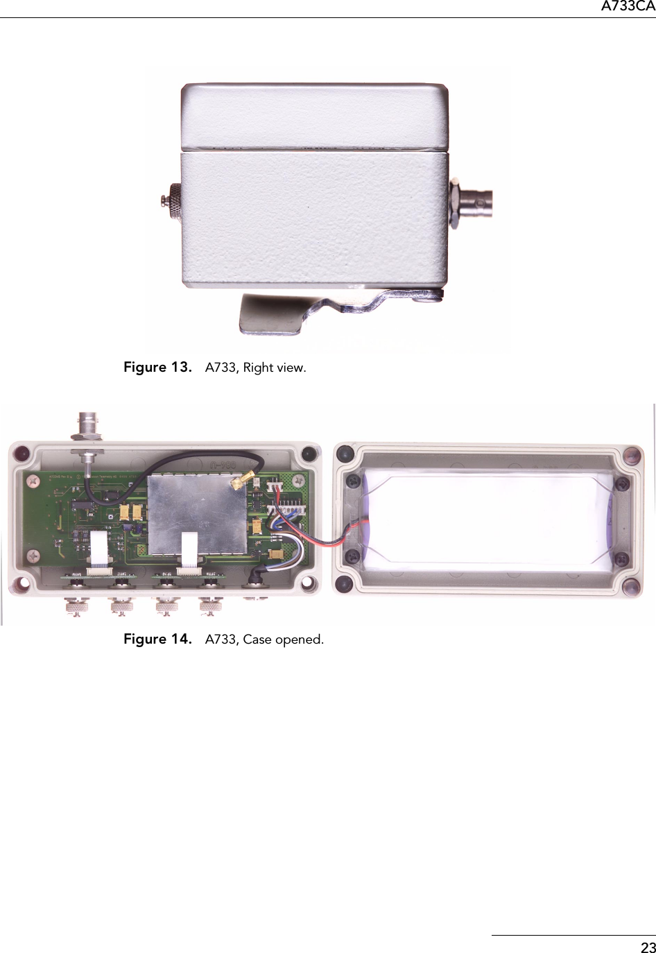
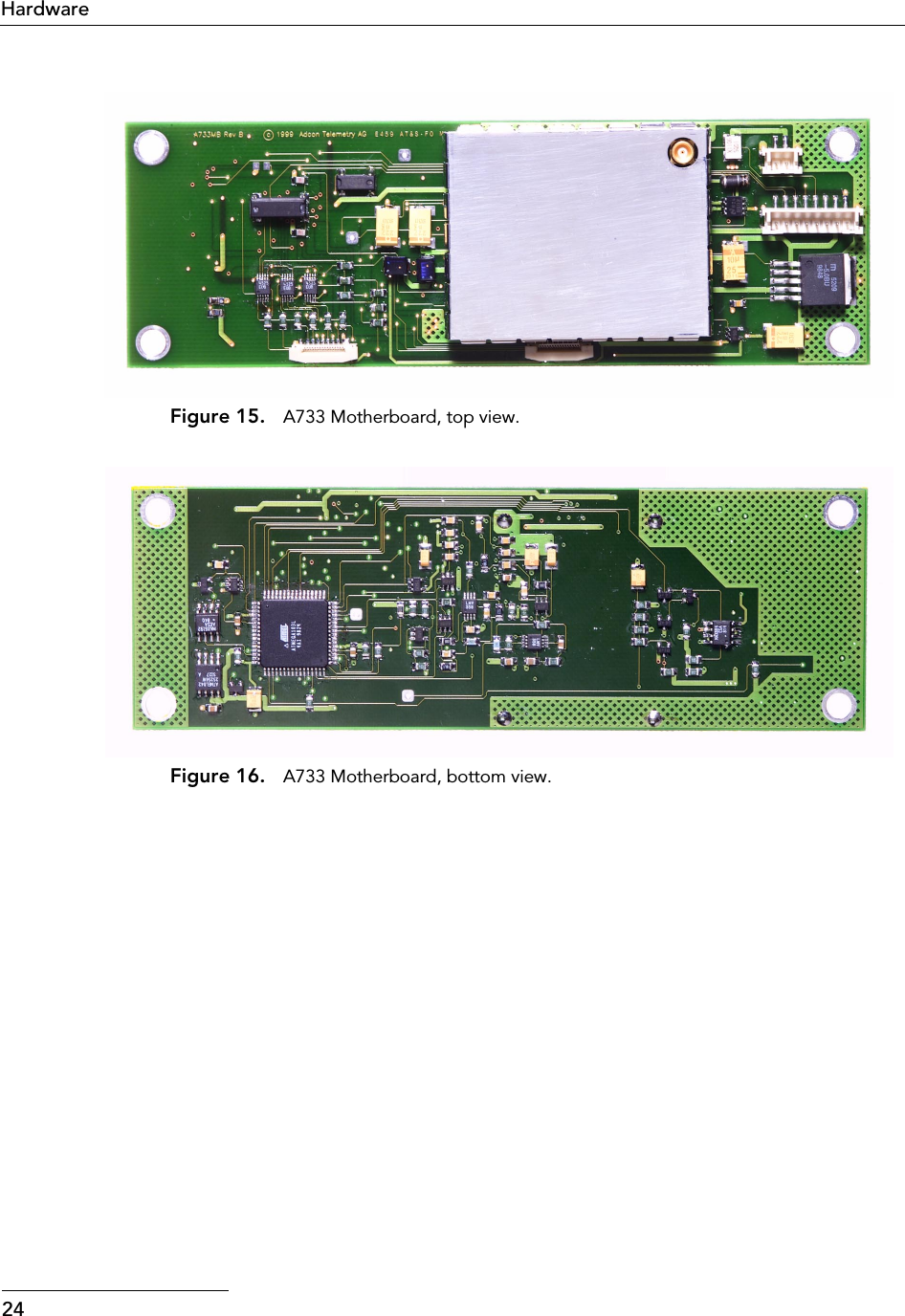
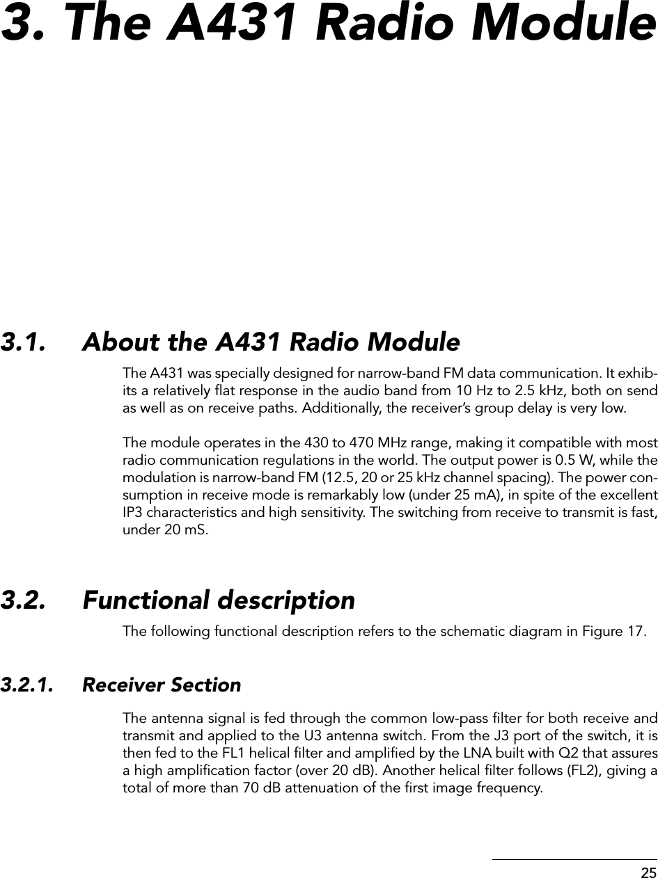
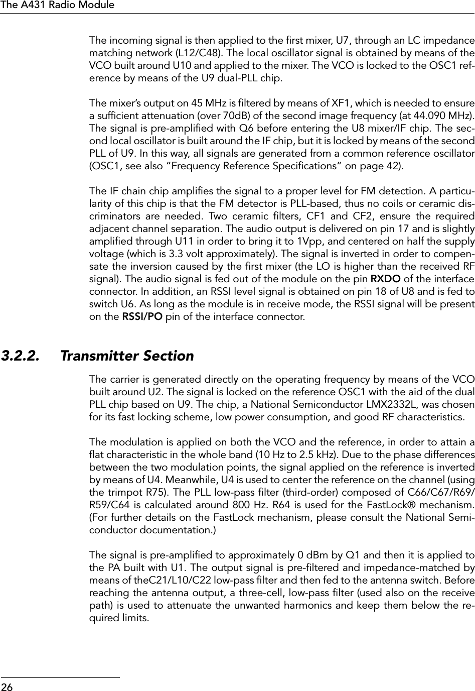
Adcon Telemetry A733 Remote Telemetry Unit User Manual A733SpecsTUV
Adcon Telemetry Inc Remote Telemetry Unit A733SpecsTUV
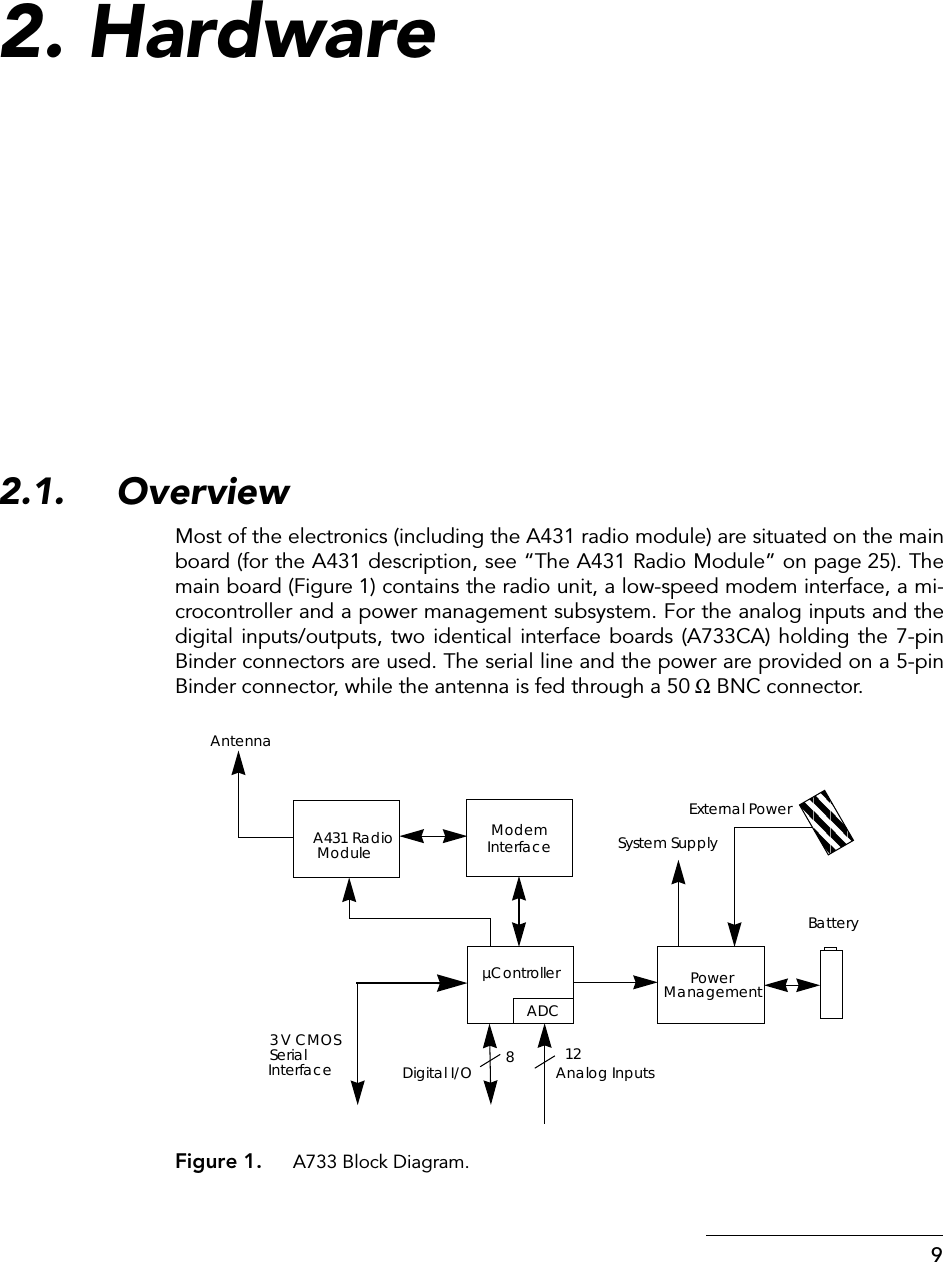
UserManual.wiki
>
Adcon Telemetry
>
A733 User Manual
Revised technical manual and photos with schematics and bill of materials removed
Navigation menu
Upload a User Manual
Namespaces
Wiki Guide
HTML
PDF
Info
Views
User Manual
Discussion / Help
Navigation


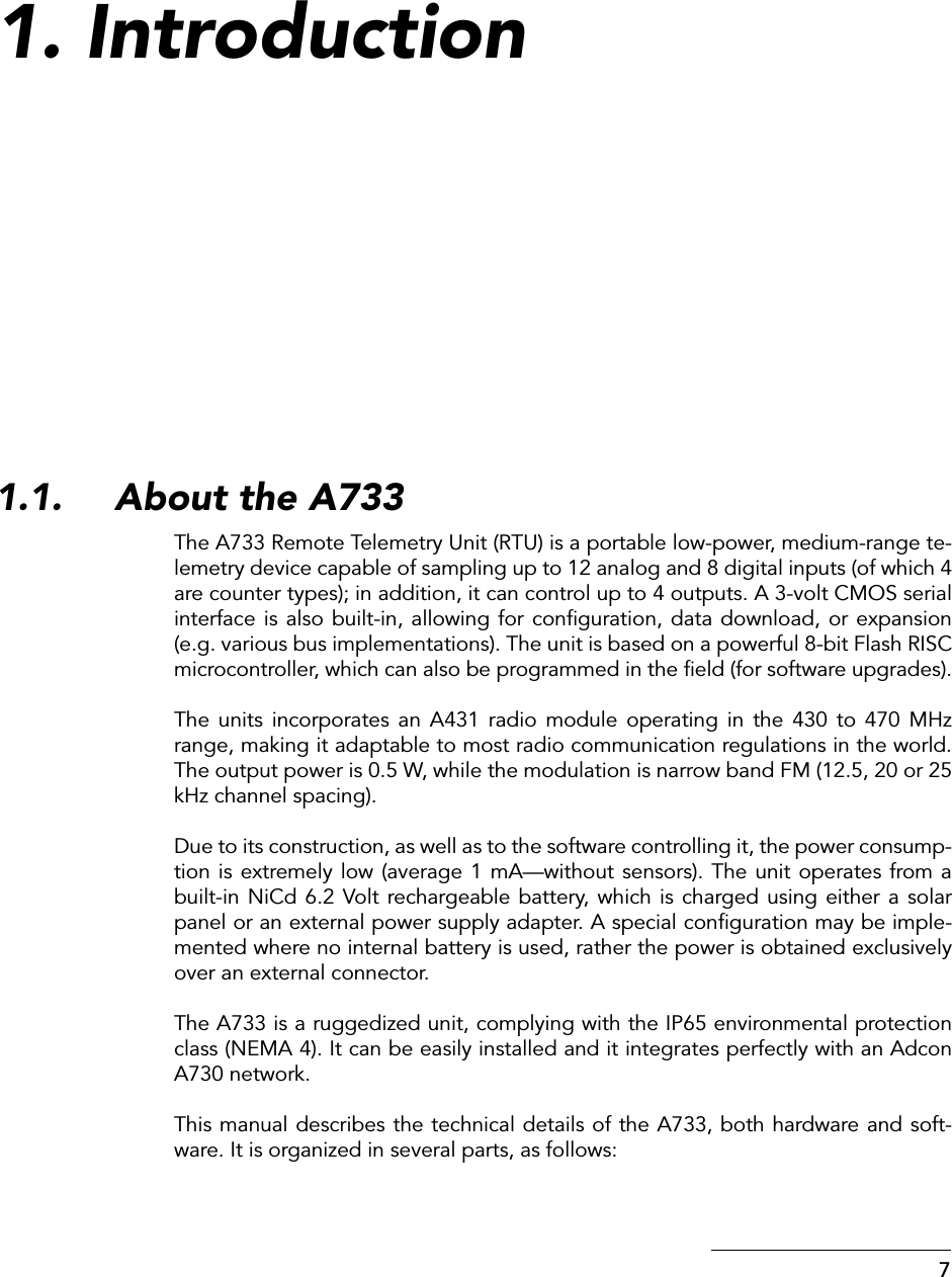
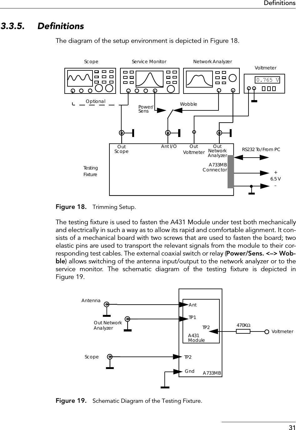
![53Commandsbattery power management (charge/discharge). To compute the actual value(in °C), the following equation must be used:•days_uptime in days; together with hr:min_uptime, it represents theamount of time the device is up without a reset or watchdog•hr:min_uptime in hours:minutes format•rssi as decimal (unsigned chars); it is the programmed value with the RSSIcommand•pmp_low and pmp_high are the programmed values with the PMP com-mand•type is used to represent the device type; following types are assigned cur-rently:— 0 for A730MD— 1 for A720— 2 for A730SD— 3 for A720B— 4 for A733•slot and samples are the actual values programmed by means of the SLOTcommand•err_level is the error value; 0 means no errorREMARKS GET only. REMOTE Yes, GET only. The A733 can issue the command both remotely and locally.EXAMPLE INFO193 INFO 255 0 18/4/1999 21:5:11 1.3 0 0 0 91 72 40 1:46 58 65 72 3 900 15 0#RXDESCRIPTION Switches the unit to permanent receive mode (for tuning purposes).PARAMETERS None.RETURNS Nothing.REMARKS The system stops, and exits the command only when a key is pressed. This com-mand returns no message.REMOTE No.EXAMPLE RX193 RX 0#Temp °C[] internalTemp 400⋅255------------------------------------------------- 6 8–=](https://usermanual.wiki/Adcon-Telemetry/A733/User-Guide-105206-Page-42.png)
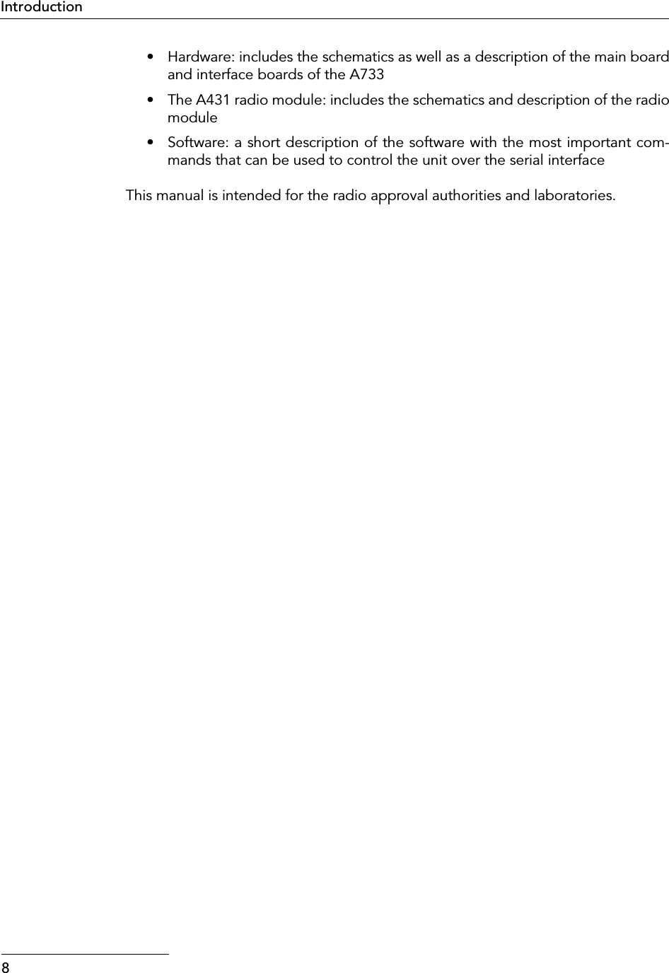
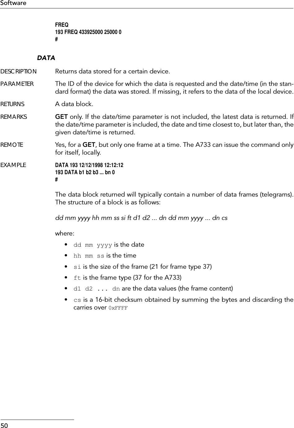
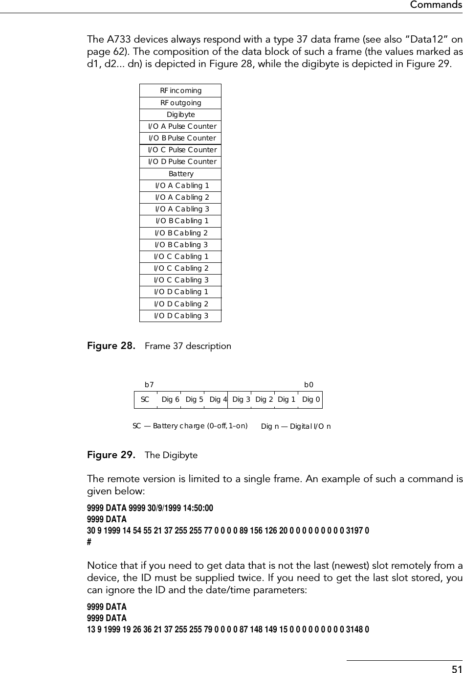
![62Software•version is the software/hardware version of the device.•clkfail and stackfail are meaningless for an A733; they are kept for histor-ical reasons.•WDT is a counter incremented each time the device was reset due to a Watch-dog timeout; its value is cleared at power-on reset.•batt is the battery voltage (this value will be also found in the Data frame).•internalTemp is the temperature in the A733 housing; the precision of thesensing element is vry low (±2C°), but it is sufficient for battery power man-agement (charge/discharge). To compute the actual value (in C°), the follow-ing equation must be used:•uptime is the time elapsed since the last reset (including a Watchdog reset).•rssi is the programmed RSSI threshold value.•pmp_low and pmp_high are the programmed power management parameters.•type is the type of the device (will return always 4 – for A733).Note: Some of the values described above are specific to the A733. The implemen-tation of the Pong frame, as well as its length (number of bytes), may vary from one device type to another.SEE ALSO Ping frame.FdevID 32FORMAT The data frame body is empty.DESCRIPTION This frame requests that a remote clear its data memory (format). The remote willanswer with a General acknowledge frame. An A733 will never issue this frame type,but it will execute and answer it.SEE ALSO General Acknowledge frame.Data12ID 37FORMAT struct {unsigned char RF_levelIn;unsigned char RF_levelOut;time_t slot_timeStamp;unsigned char digibyte;unsigned int counter0; /* Pulse Counter I/O A input */unsigned int counter1; /* Pulse Counter I/O B input */unsigned int counter2; /* Pulse Counter I/O C input */Temp °C[] internalTemp 400⋅255------------------------------------------------- 6 8–=](https://usermanual.wiki/Adcon-Telemetry/A733/User-Guide-105206-Page-51.png)
![63Frame Typesunsigned int counter3; /* Pulse Counter I/O D input */unsigned char battery;unsigned int analog_data[9];} data_frame;DESCRIPTION This frame will be sent back by the device as an answer to the Request frame.•RF_levelIn is the left zero (it is a placeholder and will be filled by the first de-vice receiving the frame).•RF_levelOut is the RF level measured by the device on the Request frame.•slot_timeStamp is the actual time stamp on the data sent.•digibyte represents the result of OR-ing the following bits:— SC represents the battery charge switch’ status.— DIG0 to DIG7 are the I/O pins on the I/O connectors. Note that only thefirst 4 DIGs are usable (there are only four I/O connectors on the A733).Note: For additional info on the bits in the digibyte, check the hardware section of this manual.•counter0 to counter3 are the values of the pulse counters.•battery is the value of the main power supply; its actual value can be com-puted using the equation:•analog_data[9] is an array of 8 unisgned integers that represents the result ofpacking the 12 12-bit values. These are the values returned by the internal A/D converter from the respective I/O connectors (see the hardware sectionfor more details). The packing mechanism is depicted below:SEE ALSO Request frame.Set IDID 40SC Dig6 Dig5 Dig4 Dig3 Dig2 Dig1 Dig0b0b7Batt V[] battery 20×255-------------------------------=16 bit values8 bit packed valuesInteger 0 Integer 1 Integer 2 Integer 312 bits 12 bits 12 bits 12 bitsByte 0 Byte 1 Byte 2 Byte 3 Byte 6Byte 5Byte 4 Byte 16 Byte 17](https://usermanual.wiki/Adcon-Telemetry/A733/User-Guide-105206-Page-52.png)