Adcon Telemetry A733 Remote Telemetry Unit User Manual A733SpecsTUV
Adcon Telemetry Inc Remote Telemetry Unit A733SpecsTUV
Revised technical manual and photos with schematics and bill of materials removed

ADCON
TELEMETRY
SMART WIRELESS SOLUTIONS
A733 RTU
Technical Reference (Type Approval)

ADCON
TELEMETRY
ADCON TELEMETRY AG
INKUSTRASSE 24
A-3400 KLOSTERNEUBURG
AUSTRIA
TEL: +43 (2243) 38 280-0
FAX: +43 (2243) 38 280-6
http://www.adcon.at
ADCON TELEMETRY INC
1001 YAMATO ROAD
SUITE #305, BOCA RATON
FL 33431 USA
TEL: +1 (561) 989-5309
FAX: +1 (561) 989-5310
http://www.adcon.com
ADCON TELEMETRY SRL
BD. ION IONESCU DELABRAD 8
R-71592 BUCHAREST
ROMANIA
TEL: +40 (1) 490-6083
FAX: +40 (1) 490-6086
http://www.adcon.ro
Proprietary Notice:
The Adcon logo, the A730 series, A720 series and addIT™, A733 series and
addWAVE, addVANTAGE and AgroExpert™ are trademarks or registered
trademarks of Adcon Telemetry AG. All other registered names used through-
out this publication are trademarks of their respective owners.
This publication contains confidential information, property of Adcon Teleme-
try AG. Disclosure to third parties of the information contained herein is pro-
hibited. Neither the whole nor any part of the information contained in this
publication may be reproduced in any material form except with the prior writ-
ten permission of Adcon Telemetry AG.
Release 1.0, December 14, 1999
Copyright ©1999 by Adcon Telemetry AG.
All rights reserved.

3
Table of Contents
Introduction ____________________________________________________7
About the A733 ______________________________________________________________ 7
Hardware _______________________________________________________9
Overview_____________________________________________________________________ 9
The Modem Interface _________________________________________________________________ 10
The Microcontroller and the Power Management Sections _________________________________ 10
The Analog + Digital I/O Interface Board ________________________________________________ 13
The Power Supply and the Serial Interface _______________________________________________ 13
External Power Supply_________________________________________________________________ 14
Specifications________________________________________________________________15
PCB Parts Placement (A733) __________________________________________________16
Bills of Materials _____________________________________________________________17
A733MB _____________________________________________________________________________ 17
A733CA _____________________________________________________________________________ 19
A733 Device’s Photographs___________________________________________________20
The A431 Radio Module _______________________________________ 25
About the A431 Radio Module________________________________________________25
Functional description________________________________________________________25
Receiver Section ______________________________________________________________________ 25
Transmitter Section____________________________________________________________________ 26

4
Manufacturing Issues ________________________________________________________ 28
Marking and labeling issues ____________________________________________________________ 28
Alignment Range and Switching Range __________________________________________________ 28
Tuning Procedure _____________________________________________________________________ 29
Setting Up the Default Parameters ______________________________________________________ 29
Commands valid for all bands ____________________________________________________ 30
Commands required for band 1 __________________________________________________ 30
Commands required for band 2 __________________________________________________ 30
Commands required for band 3 __________________________________________________ 30
Commands required for band 4 __________________________________________________ 30
Definitions ___________________________________________________________________________ 31
Test Equipment Settings _______________________________________________________________ 32
Network Analyzer (HP 8712 or equivalent)_____________________________________________ 32
Service Monitor (Rohde & Schwarz CMS50 or equivalent) _______________________________ 32
Trimming Elements____________________________________________________________________ 33
Adjusting the Receiver Front End _______________________________________________________ 33
Adjusting the VCOs ___________________________________________________________________ 34
Adjusting the Crystal Reference _________________________________________________________ 35
Checking the Receiver Parameters ______________________________________________________ 35
Checking the Transmitter Parameters ____________________________________________________ 35
Data Transfer Check ___________________________________________________________________ 36
PCB Parts Placement_________________________________________________________ 37
Bill of Materials (A431) _______________________________________________________ 38
Frequency Reference Specifications ___________________________________________ 42
A431 Module’s Photographs _________________________________________________ 43
Software ______________________________________________________45
Short Description____________________________________________________________ 45
Tasks _______________________________________________________________________ 45
Controlling the Unit__________________________________________________________ 47
Serial Communication Protocol _________________________________________________________ 47
General Format of a Command _________________________________________________________ 47
General Format of an Answer___________________________________________________________ 48
Commands___________________________________________________________________________ 48
CMDS _____________________________________________________ 48
TIME _____________________________________________________ 49
BL ____________________________________________________________________________ 49
FREQ _________________________________________________________________________ 49
DATA _________________________________________________________________________ 50
IMME _________________________________________________________________________ 52

5
INFO _________________________________________________________________________ 52
RX ___________________________________________________________________________ 53
TX ___________________________________________________________________________ 54
B ____________________________________________________________________________ 54
Returned errors list____________________________________________________________________ 54
Command line interpreter _______________________________________________________ 54
Device descriptors and storage handler ___________________________________________ 55
Real time clock ________________________________________________________________ 55
Radio interface ________________________________________________________________ 55
Notifications __________________________________________________________________ 55
Adcon Packet Radio Protocol _________________________________________________56
Digital Squelch _______________________________________________________________________ 56
Modulation Technique Used____________________________________________________________ 57
Generic Format of a Radio Frame _______________________________________________________ 57
Data Frames _________________________________________________________________________ 59
Frame Types _________________________________________________________________________ 59
Request ______________________________________________________________________ 59
Broadcast Answer ______________________________________________________________ 60
Broadcast Request _____________________________________________________________ 60
Ping __________________________________________________________________________ 61
Pong _________________________________________________________________________ 61
Fdev _________________________________________________________________________ 62
Data12 _______________________________________________________________________ 62
Set ID ________________________________________________________________________ 63
Set Slot Time and Sample Rate __________________________________________________ 64
Set Frequency _________________________________________________________________ 64
Set Battery Charge Levels _______________________________________________________ 65
General Acknowledge __________________________________________________________ 65

6

7
1. Introduction
1.1. About the A733
The A733 Remote Telemetry Unit (RTU) is a portable low-power, medium-range te-
lemetry device capable of sampling up to 12 analog and 8 digital inputs (of which 4
are counter types); in addition, it can control up to 4 outputs. A 3-volt CMOS serial
interface is also built-in, allowing for configuration, data download, or expansion
(e.g. various bus implementations). The unit is based on a powerful 8-bit Flash RISC
microcontroller, which can also be programmed in the field (for software upgrades).
The units incorporates an A431 radio module operating in the 430 to 470 MHz
range, making it adaptable to most radio communication regulations in the world.
The output power is 0.5 W, while the modulation is narrow band FM (12.5, 20 or 25
kHz channel spacing).
Due to its construction, as well as to the software controlling it, the power consump-
tion is extremely low (average 1 mA—without sensors). The unit operates from a
built-in NiCd 6.2 Volt rechargeable battery, which is charged using either a solar
panel or an external power supply adapter. A special configuration may be imple-
mented where no internal battery is used, rather the power is obtained exclusively
over an external connector.
The A733 is a ruggedized unit, complying with the IP65 environmental protection
class (NEMA 4). It can be easily installed and it integrates perfectly with an Adcon
A730 network.
This manual describes the technical details of the A733, both hardware and soft-
ware. It is organized in several parts, as follows:

8
Introduction
• Hardware: includes the schematics as well as a description of the main board
and interface boards of the A733
• The A431 radio module: includes the schematics and description of the radio
module
• Software: a short description of the software with the most important com-
mands that can be used to control the unit over the serial interface
This manual is intended for the radio approval authorities and laboratories.
9
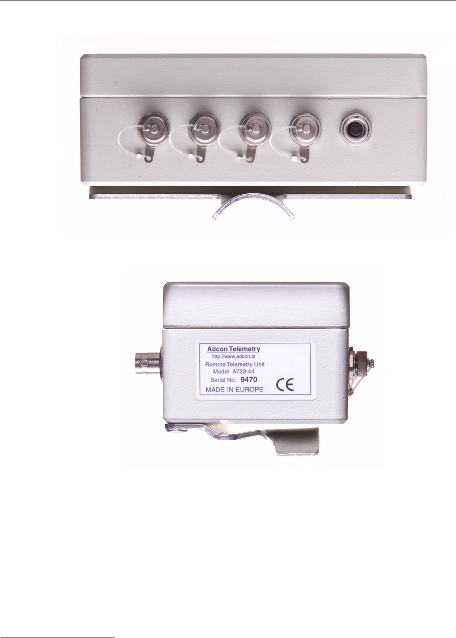
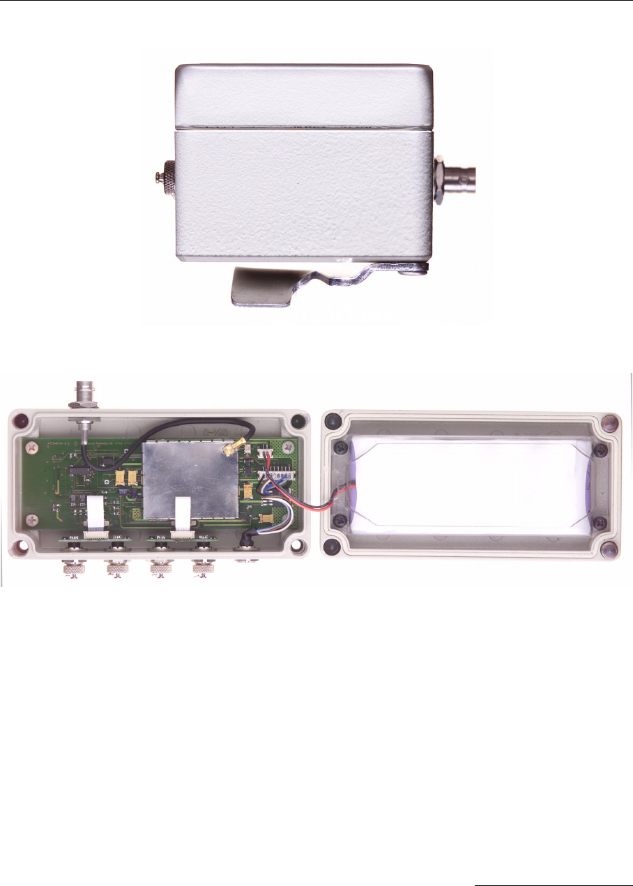
2. Hardware
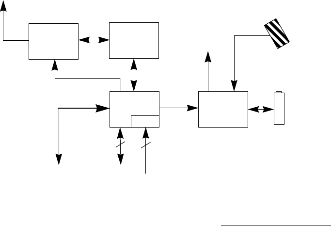
2.1. Overview
Most of the electronics (including the A431 radio module) are situated on the main
board (for the A431 description, see “The A431 Radio Module” on page 25). The
main board (Figure 1) contains the radio unit, a low-speed modem interface, a mi-
crocontroller and a power management subsystem. For the analog inputs and the
digital inputs/outputs, two identical interface boards (A733CA) holding the 7-pin
Binder connectors are used. The serial line and the power are provided on a 5-pin
Binder connector, while the antenna is fed through a 50
Ω
BNC connector.
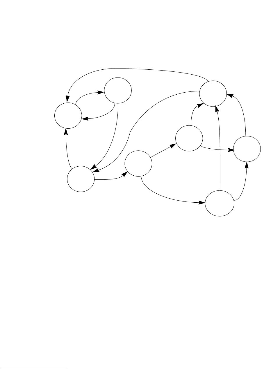
Figure 1.
A733 Block Diagram.
A431 Radio
Antenna
µController
Modem
Interface
Power
Management
System Supply
Battery
External Power
ADC
12
8Analog Inputs
Digital I/O
3 V CMOS
Interface
Module
Serial

10
Hardware
For further details, consult the schematic diagram in Figure 2.
2.1.1. The Modem Interface
The modem operates with two tones: 1 kHz (representing the “1” bits) and 2 kHz
(representing the “0” bits). A bit cell is represented by a complete time period (
1/f
),
thus the raw throughput varies between 1 and 2 kbps (average 1.5 kbps). The mo-
dem functions are essentially implemented in software. However, a signal condition-
ing is performed on both receive and transmit paths.
On receive, the buffered analog data signal from the radio unit is applied to a 3 kHz
low pass filter (U6). The filter output is further fed both to a Schmidt trigger (U5:A)
and a 100 Hz low-pass filter (U5:B), the output of the latter being used as a reference
for the slicer (the Schmidt trigger). The TTL data,
RXDO
, is obtained at the output
of the slicer (i.e. on TP1). The microcontroller overtakes the decoding operation (see
also “Modulation Technique Used” on page 57).
On transmit, a two-poles low-pass filter (U11) is used: its role is to “smooth” the
square signal
TXDI
generated by the microcontroller. Before entering the filter, a
microprocessor-controlled, variable-gain amplifier built with U12/U13 is used to set
the modulation level for different bandwidths (12.5, 20 or 25 kHz). The selected val-
ue is stored in the microcontroller’s EEPROM during the aligning procedure.
2.1.2. The Microcontroller and the Power Management Sections
The operation of the whole unit is under the control of U9, an Atmel ATMega 103
microcontroller. It is a powerful chip exhibiting a very low power consumption. Its
main functions are:
• Controls the radio unit
• Implements the modem functionality
• Assembles the radio frames and waits for requests from a remote
• Performs the sampling of the sensor inputs and the A/D conversion
• Stores the values in a local FIFO; manages the FIFO
• Implements the pulse counter function
• Manages the real-time clock
• Assures the power management
• Implements a serial Command Line Interface (CLI)
The chip operates at its maximum speed, in this case 4 MHz (the “L” version), and
uses a crystal (X2) for the on-board clock generator. The real time clock is imple-
mented by means of a 32.768 kHz crystal (X1) connected on the internal Timer/
Counter0.

11
The Microcontroller and the Power Management Sections
The radio unit is controlled via the SPI bus (to set the PLL chip parameters) and via
several ports of the microcontroller for such operations as transmit and receive. In
addition, the high current 5 volt LDO voltage source (U4) is switched on before the
radio module’s PA must be activated.The modem’s output (implemented in soft-
ware) is available on PB5 (
TXDI
), while the receiver output is fed to PD4 (
RXDO
).
The A/D subsystem is used to sample the inputs (ADC0 to ADC5); the 6th and 7th
analog input are used for on-board measurements as local battery, internal temper-
ature and
RSSI/PO
signal; the battery and temperature voltages are switched by
means of the analog switch U19. A stable 2.5 Volt reference supplied by U8 is ap-
plied to the A
ref
pin. The reference is powered by the microcontroller only when
sampling the A/D inputs. The external sensors are powered through U17. In order
to enlarge the maximum number of sensors sampled, several analog multiplexers
are used (U3/U7/U10). After sampling the A/D once, the software switches the mul-
tiplexers (using the signal
MUX
, pin PD2) and samples the inputs once again, thus
doubling to 12 the maximum number of analog inputs.
The sampled input values are stored in a FIFO memory based on a serial EEPROM
chip, U18. These values may be retrieved when a request is received over radio, or
over the serial line. The configuration parameters (e.g. the serial number of the de-
vice, the operating frequency, etc.) are stored in the microcontroller’s on-chip EE-
PROM.
The pulse counter functionality is implemented by means of the four interrupt inputs
INT4 to INT7 of the ATMega 103 microcontroller.
The power management supervises the charge/discharge of the battery (via Q1 and
half of U15), senses when it reaches the “misery” state and switches off the unit in
order to protect the battery (second half of U15). In addition, the software senses the
unit’s idle state (e.g. the unit is in a warehouse in storage condition), where no activ-
ities must be performed thus driving the unit into hibernation. If the unit is switched
off due to an extremely low battery level, Q2 would start it up again only if external
power is applied to the power connector (e.g. from a solar panel).
The terminal mode is implemented by means of the built-in UART. No on-board lev-
el drivers are present in order to minimize power consumption; a special adapter ca-
ble that performs the CMOS to RS232 level shift is available. By means of this cable
and using the implemented commands, various parameters can be changed/config-
ured.
A brown-out supervisor chip (U14) is used to assure a smooth start-up of the micro-
controller and avoid possible erratic behavior when the battery level descends be-
low the minimum operating value (2.7 volts). The same chip activates the write-
protect signal of the serial EEPROM during reset, in order to protect the data in the
EEPROM.

13
The Analog + Digital I/O Interface Board
2.1.3. The Analog + Digital I/O Interface Board
The two identical interface boards ensure the connection between the main board
and the outside world (see Figure 3). The interface boards contain two connectors
each (
I/O A
and
I/O B
or
I/O C
and
I/O D
respectively) and some active/passive
components protecting the inputs. Each of the
I/O
connectors can accept:
• Three analog inputs
• One digital Input or Output (its function can be switched under program con-
trol, also remotely)
• One pulse counter input
Depending on the way R3 and R4 are populated, the power supply to the I/O de-
vices can be either switched or permanent. This option is factory programmable
only. If R3 is populated, the power will be permanently applied to the sensors while
if R4 is populated, the power will be applied for a defined time (typically 2 seconds)
only shortly before the microcontroller samples the inputs.
2.1.4. The Power Supply and the Serial Interface
The
POWER
connector allows for:
• External supply (battery or any DC source from
5.6 to 10 volts)
• External charge supply (either a solar panel or
an AC adapter) if an internal rechargeable bat-
tery is used
• Communication over serial lines, at 19200 baud
Note: The serial line is 3 volt CMOS compatible, therefore a special adapter cable
must be used to reach the RS-232 levels. Also, if an external battery is used,
the internal battery must be disconnected.
RxD
TxD
Ground
Battery
Ext Power
1
2
3
45
15
External Power Supply
when the battery voltage drops below 5.6 Volts, and under 5.9 Volts the RF opera-
tion may stop.
Figure 4.
Connection of an external power supply.
2.2. Specifications
The A733 fulfills the specifications of the EN 300 220-1, Class 12, ETS 300 086 and
ETS 300 113, as well as the FCC Part 90.214 (Subpart J) of the CFR 47.
Note: The parameters below were measured with the A733 + A431 combination.
Parameter Min Typ Max Unit
Common
Supply 5.6 6.2 10.0 V
Operating Temperature -30 +70 °C
Relative Humidity 99 %
Class Protection IP65
Data Rate (Using the On-board Software Modem) 1000 1500
a
2000 bps
Operating Frequency (-44 version)
b
430 450 MHz
Operating Frequency (-46 version)
b
450 470 MHz
Frequency Stability (-20 to +50°C) ±1.5 kHz
Frequency Stability (-30 to +60°C) ±2.5 kHz
Receiver
Sensitivity (12 db S/S+N) -118 dBm
Image Frequency Attenuation (1st IF = 45 MHz) -70 dB
POWER
I/O C
I/O D
+
-
Black
Red
5 to 10 Volt
RS232
+
+
Power Cable Serial Adapter Cable
I/O A
I/O B
ANT
16
Hardware
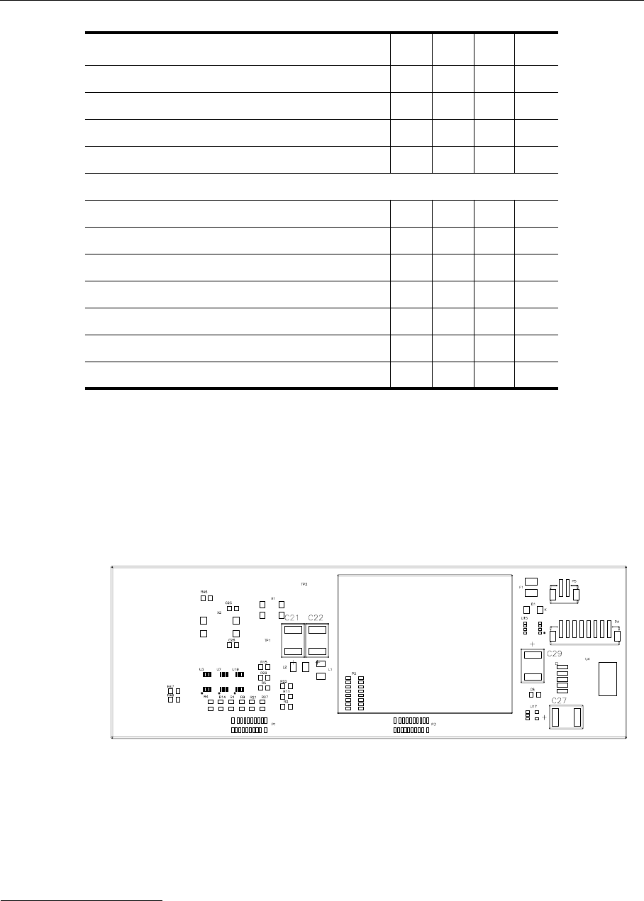
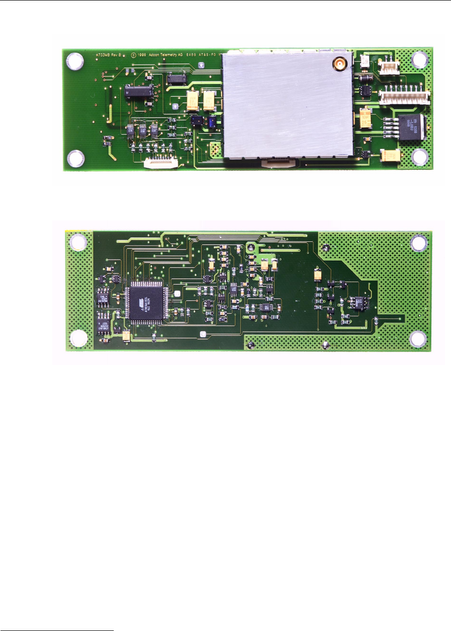
2.3. PCB Parts Placement (A733)
Figure 5.
A733MB Parts placement (top).
Local Oscillator Leakage 2 nW
Adjacent Channel Attenuation -70 dB
RSSI dynamic 90 dB
Operating Current (incl. On-board Microcontroller) 25 mA
Transmitter (all measurements made on a 50
Ω
resistive load)
Output Power 27 dBm
Spurious Radiation 200 nW
Adjacent Channel Power (12.5 kHz version) -34 dBm
Adjacent Channel Power (25 kHz version) -44 dBm
Occupied Bandwidth (12.5 kHz version) 7.0 kHz
Occupied Bandwidth (25 kHz version) 12 kHz
Operating Current (incl. On-board Microcontroller) 600 mA
a. Data rate is content dependent.
b. This parameter represents the alignment range; the switching range can
be limited in the software to a narrower space (even to the extent of a
single channel).
Parameter Min Typ Max Unit
21
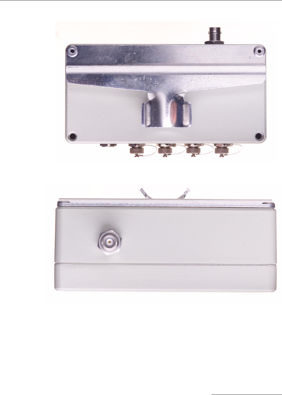
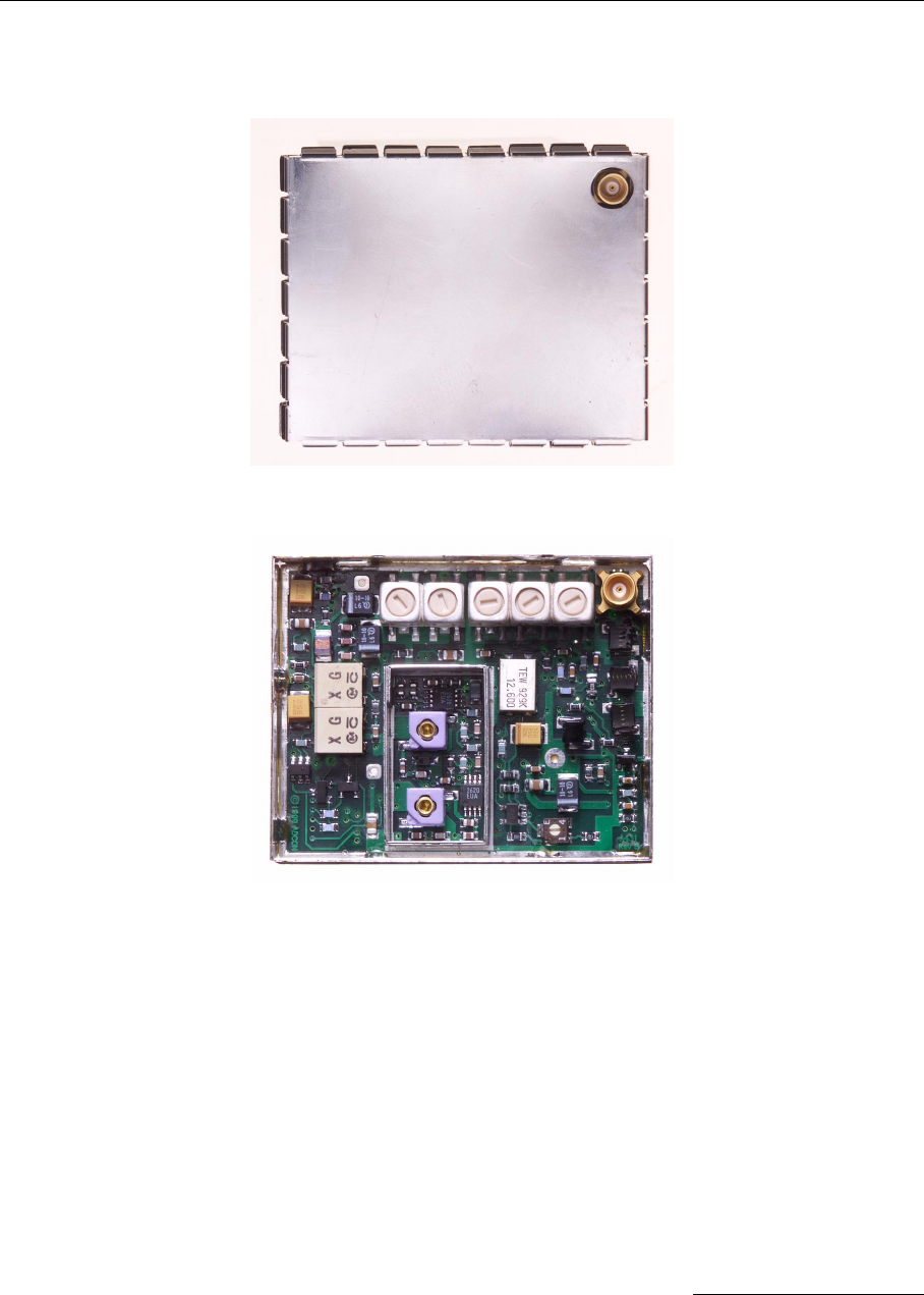
A733CA
Figure 9.
A733, Back view.
Figure 10.
A733, Top view.
22
Hardware
Figure 11.
A733, Bottom view.
Figure 12.
A733, Left view.
23
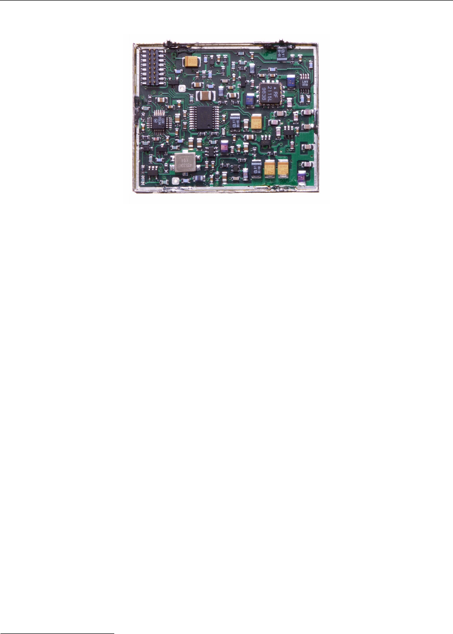
A733CA
Figure 13.
A733, Right view.
Figure 14.
A733, Case opened.
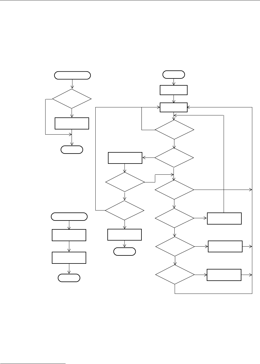
24
Hardware
Figure 15.
A733 Motherboard, top view.
Figure 16.
A733 Motherboard, bottom view.

25
3. The A431 Radio Module
3.1. About the A431 Radio Module
The A431 was specially designed for narrow-band FM data communication. It exhib-
its a relatively flat response in the audio band from 10 Hz to 2.5 kHz, both on send
as well as on receive paths. Additionally, the receiver’s group delay is very low.
The module operates in the 430 to 470 MHz range, making it compatible with most
radio communication regulations in the world. The output power is 0.5 W, while the
modulation is narrow-band FM (12.5, 20 or 25 kHz channel spacing). The power con-
sumption in receive mode is remarkably low (under 25 mA), in spite of the excellent
IP3 characteristics and high sensitivity. The switching from receive to transmit is fast,
under 20 mS.
3.2. Functional description
The following functional description refers to the schematic diagram in Figure 17.
3.2.1. Receiver Section
The antenna signal is fed through the common low-pass filter for both receive and
transmit and applied to the U3 antenna switch. From the J3 port of the switch, it is
then fed to the FL1 helical filter and amplified by the LNA built with Q2 that assures
a high amplification factor (over 20 dB). Another helical filter follows (FL2), giving a
total of more than 70 dB attenuation of the first image frequency.

26
The A431 Radio Module
The incoming signal is then applied to the first mixer, U7, through an LC impedance
matching network (L12/C48). The local oscillator signal is obtained by means of the
VCO built around U10 and applied to the mixer. The VCO is locked to the OSC1 ref-
erence by means of the U9 dual-PLL chip.
The mixer’s output on 45 MHz is filtered by means of XF1, which is needed to ensure
a sufficient attenuation (over 70dB) of the second image frequency (at 44.090 MHz).
The signal is pre-amplified with Q6 before entering the U8 mixer/IF chip. The sec-
ond local oscillator is built around the IF chip, but it is locked by means of the second
PLL of U9. In this way, all signals are generated from a common reference oscillator
(OSC1, see also “Frequency Reference Specifications” on page 42).
The IF chain chip amplifies the signal to a proper level for FM detection. A particu-
larity of this chip is that the FM detector is PLL-based, thus no coils or ceramic dis-
criminators are needed. Two ceramic filters, CF1 and CF2, ensure the required
adjacent channel separation. The audio output is delivered on pin 17 and is slightly
amplified through U11 in order to bring it to 1Vpp, and centered on half the supply
voltage (which is 3.3 volt approximately). The signal is inverted in order to compen-
sate the inversion caused by the first mixer (the LO is higher than the received RF
signal). The audio signal is fed out of the module on the pin RXDO of the interface
connector. In addition, an RSSI level signal is obtained on pin 18 of U8 and is fed to
switch U6. As long as the module is in receive mode, the RSSI signal will be present
on the RSSI/PO pin of the interface connector.
3.2.2. Transmitter Section
The carrier is generated directly on the operating frequency by means of the VCO
built around U2. The signal is locked on the reference OSC1 with the aid of the dual
PLL chip based on U9. The chip, a National Semiconductor LMX2332L, was chosen
for its fast locking scheme, low power consumption, and good RF characteristics.
The modulation is applied on both the VCO and the reference, in order to attain a
flat characteristic in the whole band (10 Hz to 2.5 kHz). Due to the phase differences
between the two modulation points, the signal applied on the reference is inverted
by means of U4. Meanwhile, U4 is used to center the reference on the channel (using
the trimpot R75). The PLL low-pass filter (third-order) composed of C66/C67/R69/
R59/C64 is calculated around 800 Hz. R64 is used for the FastLock® mechanism.
(For further details on the FastLock mechanism, please consult the National Semi-
conductor documentation.)
The signal is pre-amplified to approximately 0 dBm by Q1 and then it is applied to
the PA built with U1. The output signal is pre-filtered and impedance-matched by
means of theC21/L10/C22 low-pass filter and then fed to the antenna switch. Before
reaching the antenna output, a three-cell, low-pass filter (used also on the receive
path) is used to attenuate the unwanted harmonics and keep them below the re-
quired limits.

28
The A431 Radio Module
An Automatic Level Control (ALC) system is responsible for keeping the output pow-
er constant, regardless of the external influences (temperature, VCO excitation and/
or supply). A small part of the RF energy is rectified by D2 and applied to the U5:A
amplifier. By means of U5:B, the power is controlled according to the pre-set power
level (ALC input). U5:A is basically an analog comparator between the actual and the
programmed power output. Depending on the error signal obtained, a variable volt-
age is applied on the PD input of the PA chip, thus effectively controlling its output
power. In addition, the actual power output level is fed to the U6 analog switch and
presented to the RSSI/PO output while the unit is switched in transmit mode.
The modulation is applied on two-points: the VCO and the reference oscillator—this
is needed to obtain a flat response in the audio range from 10Hz to 2.5 kHz and com-
pensate for the counter-effect opposed by the synthesizer loop. The input signal
(must be 1 Vpp) is fed through a resistive divider (R14/R13) to the “cold” end of the
varactor diode controlling the VCO (D1). At the same time, the same modulation
signal is applied to the inverting op-amp U4 and then to the OSC1 reference oscil-
lator (a VCTCXO). The modulation signal is inverted in order to bring it in phase with
the VCO modulation point.
3.3. Manufacturing Issues
3.3.1. Marking and labeling issues
The A431 Module is manufactured in two versions:
• Low band—able to operate between 430 and 450 MHz
• High band—able to operate between 450 and 470 MHz
From a manufacturing perspective, the difference between the high and low band
are the two helical filters FL1 and FL2 used on the receiving chain. The low band ver-
sion is marked as A733-44 while the high band is marked as A733-46.
3.3.2. Alignment Range and Switching Range
The A431 radio module’s alignment range is 20 MHz, while the switching range is
10 MHz. According to the definitions formulated in the ETS 300086 and ETS 300013
specifications, the A431 radio module belongs to the AR1 category. Therefore, for
the European testing, two units should be presented for test purposes, as follows:
• One A733 unit containing an A431-44 radio module, alignment range 430-
450 MHz, switching range 435-455 MHz
• One A733 unit containing an A431-46 radio module, alignment range 450-
470 MHz, switching range 455-465 MHz.
Consequently, two test reports will be provided to Adcon Telemetry AG.

29
Tuning Procedure
For North America (FCC), only the portion 460 to 470 MHz will be used; therefore,
a single device model A733-46 having the switching range between 460 and 470
MHz will be submitted for testing.
3.3.3. Tuning Procedure
The A431 modules are to be tuned by mounting them on a test fixture consisting of
a specially modified A733 motherboard. The modification refers to certain mechan-
ical aspects, in order to provide an easy plug in and out of the control connector (P2)
as well as to the TP1 and TP2 test points.
The alignment operation must differentiate between following classes of units:
• Band 1: from 430 to 440 MHz
• Band 2: from 440 to 450 MHz
• Band 3: from 450 to 460 MHz
• Band 4: from 460 to 470 MHz
Note: The boards differ only through the FL1 and FL2, in that Band 1 and 2 use
models TOKO 493S-1071A and 492S-1056A while Band 3 and 4 use models
TOKO 493S-1075A and 492S-1060A, respectively. In addition, the tuning pro-
cedure and some software parameters differ. The differences are clearly stat-
ed in the following paragraphs, where applicable.
3.3.4. Setting Up the Default Parameters
The tuning procedure is not possible without first configuring some default param-
eters for the A733 motherboard used in the testing fixture. This is done via the serial
interface of the motherboard by using a communication terminal program (e.g. Hy-
perterminal, in Microsoft® Windows™ 95). The terminal program must be config-
ured as follows:
• 19200 Baud
• 1 Stop bit
• No parity
• No protocol (neither hardware, nor software)
To check if the communication is operational, press the
ENTER key. An
nnnn 0
#
prompt should appear on the terminal screen (
nnnn
is the actual ID of the unit that
is printed on its label). The following default parameters must be pre-loaded (for
more information about the meaning of the commands, consult the section “Com-
mands” on page 48):
RxD
TxD
Ground
Battery
Ext Power
1
2
3
45

30
The A431 Radio Module
Commands valid for all bands
ID 1
PMP 65 72
SLOT 900 15
RSSI 58
Commands required for band 1
TF 430000000
BL 430000000 440000000
FREQ 430000000 12500
Commands required for band 2
TF 440000000
BL 440000000 450000000
FREQ 440000000 12500
Commands required for band 3
TF 450000000
BL 450000000 460000000
FREQ 450000000 12500
Commands required for band 4
TF 460000000
BL 460000000 470000000
FREQ 460000000 12500
Note: The TF command sets the start tuning frequency, the BL command sets the
band limits, and the FREQ command sets the actual operating frequency;
before shipping and depending on the target country, the last two parame-
ters may be changed. The BL command must always be issued before the
FREQ command.
31
Definitions
3.3.5. Definitions
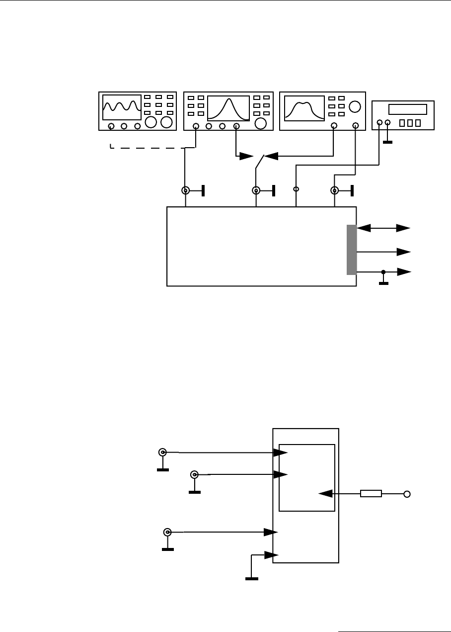
The diagram of the setup environment is depicted in Figure 18.
Figure 18. Trimming Setup.
The testing fixture is used to fasten the A431 Module under test both mechanically
and electrically in such a way as to allow its rapid and comfortable alignment. It con-
sists of a mechanical board with two screws that are used to fasten the board; two
elastic pins are used to transport the relevant signals from the module to their cor-
responding test cables. The external coaxial switch or relay (Power/Sens. <–> Wob-
ble) allows switching of the antenna input/output to the network analyzer or to the
service monitor. The schematic diagram of the testing fixture is depicted in
Figure 19.
Figure 19. Schematic Diagram of the Testing Fixture.
0.765 V
Power/
Sens Wobble
Out
Scope Ant I/O Out
Voltmeter Out
Network
Analyzer
Testing
Fixture
RS232 To/From PC
+
–
6.5 V
A733MB
Connector
Optional
Scope Service Monitor Network Analyzer Voltmeter
Scope
Out Network
Analyzer
Ant
Gnd
TP1
A733MB
TP2
TP2 Voltmeter
470KΩ
Antenna
A431
Module

32
The A431 Radio Module
3.3.6. Test Equipment Settings
Before proceeding, certain controls on the test equipment must be set; some of the
settings depend of the operating band (high or low) of the device under test (DUT).
In addition, it is highly recommended that the ambient temperature during align-
ment is kept to 24° C (±2°C).
3.3.6.1. Network Analyzer (HP 8712 or equivalent)
The settings for the Network Analyzer are as follows:
• Center frequency: 450 MHz
• Span: 100 MHz
• Display: 10.0 dB/div
• Power: -20 dBm
• Markers:
— band 1: Mkr1 – 435 MHz, Mkr2 – 430 MHz, Mkr3 – 440 MHz
— band 2: Mkr1 – 445 MHz, Mkr2 – 440 MHz, Mkr3 – 450 MHz
— band 3: Mkr1 – 455 MHz, Mkr2 – 450 MHz, Mkr3 – 460 MHz
— band 4: Mkr1 – 465 MHz, Mkr2 – 460 MHz, Mkr3 – 470 MHz
Note: It is a good idea to store the instrument state for the four settings for a rapid
recall when needed.
3.3.6.2. Service Monitor (Rohde & Schwarz CMS50 or equivalent)
The setting for the receiver section check are as follows (RX-TEST):
• SET RF: 430000000 Hz (Band 1) / 440000000 Hz (Band 2) / 450000000 Hz
(Band 3) / 460000000 Hz (Band 4)
• RF LEV: 1 µV
• SINAD
• AF1: 1kHz
• MOD1: 2.5 kHz
• SCOPE MODE
• BEST RANGE
The settings for the transmitter section check (TX-TEST):
• COUNT: (should show the transmitter carrier frequency)
• POWER: (should show the transmitter carrier power)
33
Trimming Elements
3.3.7. Trimming Elements
The location of the trimming elements on the A431 Module is shown in Figure 20.
Figure 20. Location of the trimming elements.
3.3.8. Adjusting the Receiver Front End
1. Mount the DUT (Device Under Test) on the testing fixture and connect it to the
host via the serial cable.
2. Select the appropriate instrument profile depending on the device’s band.
3. Turn the DUT in permanent receive mode by entering the RX command at the
terminal.
4. Check that the switch on the Testing Fixture is in the Wobble position.
5. Adjust the FL1 and FL2 filters (see Figure 20) until you obtain a curve similar to
the one shown in Figure 21 (depending on the band, the markers may be
different); this is done by successively adjusting the five trimming screws
located on the filters.
R75 (Crystal Reference)
FL1FL2
L15 (RX VCO)
L7 (TX VCO)
34
The A431 Radio Module
If the adjustments do not achieve the appropriate curve, check the power supply,
the cable connections to/from the test equipment, etc. Verify also that all the pins of
the FL1 and FL2 filters are properly soldered.
Figure 21. Helical Filter + LNA’s selectivity diagram.
3.3.9. Adjusting the VCOs
1. Flip the switch on the Testing Fixture to the Power/Sens. position.
2. Verify that the DUT is in receive mode (enter the RX command at the terminal
program).
3. Adjust the L15 coil (see Figure 20) until the voltage shown on the digital
voltmeter is 900 mV, ±50 mV (see also the note below).
4. Switch the unit to transmit mode by entering TX at the terminal.
5. Adjust the L7 coil (see Figure 20) until the voltage shown on the voltmeter is
again 900 mV, ±50 mV.
6. Press the enter key at the terminal to switch the unit off.
Note: A calibration may be needed due to the internal resistance of the voltmeter
and the serial resistor mounted on the Testing Fixture. The calibration is per-
formed by measuring the VCO voltage directly on the TP2 and by comparing
the value with that measured through the Testing Fixture. The values given
above are the real ones, measured directly.
If the above limits cannot be obtained, or the readout is unstable, verify the follow-
ing:
• The programmed operating frequencies are indeed 430 (Band 1), 440
(Band 2), 450 (Band 3) and 460 MHz (Band 4). To check this, type the com-
mand FREQ at the terminal prompt; the device will answer by returning the
current frequency.
• The respective commands (RX and TX) were issued.

35
Adjusting the Crystal Reference
• No parts are missing, or have the incorrect value, or are badly soldered (check
the parts around U2 and U10).
3.3.10. Adjusting the Crystal Reference
1. Flip the switch on the Testing Fixture to the Power/Sens. position.
2. Switch the unit to transmit mode by entering TX at the terminal.
3. Observe the indication shown by the Service Monitor: adjust R75 (see
Figure 20) until the carrier frequency indicates 430000000 (Band 1), 440000000
(Band 2), 450000000 (Band 3), or 460000000 MHz (Band 4) ± 200 Hz,
respectively.
3.3.11. Checking the Receiver Parameters
1. Verify that the switch on the Testing Fixture is flipped to the Power/Sens.
position.
2. Switch the DUT to receive mode by entering RX at the terminal.
3. Switch the Service Monitor to RX TEST mode, on the appropriate frequency
(430 / 440 / 450 or 460 MHz respectively); the level should be 1 µV (see also
“Test Equipment Settings” on page 32).
4. Verify that the S/N ratio is at least 12 dB; in addition, if a scope is also
connected, a clear 1 kHz sine wave should be visible, with a relatively low
amount of noise superimposed.
5. Switch the DUT to pulsed mode by pressing the Enter key. After several
seconds, you will see the image on the scope pulsing at about one-second
intervals.
6. Switch the RF generator output off.
7. Verify that the RSSI threshold is correct by typing the command RSSI; the actual
value must be lower than the threshold set. If this is not the case, repeat the
RSSI command several times—perhaps the frequency is in use (a radio receiver
set on the operating frequency would help detect foreign transmissions). If the
threshold difference is marginal, it must be increased by using the RSSI
<value> command (it must be 20 to 30% higher than the actual value).
If any of the above targets are not reachable, visually verify first that the U8 chip is
correctly soldered and that there are no shorts between its pins (most problems usu-
ally appear around this chip).
3.3.12. Checking the Transmitter Parameters
1. Verify that the switch on the Testing Fixture is flipped to the Power/Sens.
position.
2. Switch the DUT to transmit mode by typing the command TX 0 at the terminal.

36
The A431 Radio Module
3. Switch the Service Monitor to TX TEST mode, on the appropriate frequency
(430 / 440 / 450 or 460 MHz respectively). You should see the following
parameters on the Service Monitor readout:
a. Carrier: 430000000 ± 200 Hz (or 440000000 / 450000000 / 460000000
respectively)
b. Output Power: 26.5 dBm (+ 0.5 dBm / - 1 dBm)
c. Frequency Deviation: ±2.0 kHz (±0.2 kHz)
4. Switch the unit to stand-by by pressing the Enter key.
For item 3.a above, adjust R75 (see Figure 20). For item 3.b, issue the command
PWR at the terminal and use the D (down) and U (up) keys until the required value
is reached. Finally, for item 3.c, issue the command BW at the terminal and again
use the D and U keys to reach the required value.
3.3.13. Data Transfer Check
The last check is a radio data transfer. In order to perform it, at least a base station
(model A730SD) or another remote station (model A733) must be installed and op-
erated on the same test frequency, in the near vicinity (no more than 30 m).
Note: The base or remote station used for this test must be operated with a fictive
antenna (a 50
Ω
resistor).
To perform the test, enter the command B at the terminal prompt: the base and/or
remote station must answer with the RF in and out values. If an answer is not re-
ceived after several seconds, retry the command. If an answer is still not received,
then use a scope on TP1 on the A733MB board (the Text Fixture) to verify that the
digital data is present (on receive). In addition, a radio receiver tuned on the oper-
ating frequency can also supply a rough indication of whether the receiver or the
transmitter is defective.
37
Data Transfer Check
3.4. PCB Parts Placement
Figure 22. A431 Parts placement (top).
42
The A431 Radio Module
3.6. Frequency Reference Specifications
43
Data Transfer Check
3.7. A431 Module’s Photographs
Figure 24. A431 Module, General view.
Figure 25. A431 Module, Top view.
44
The A431 Radio Module
Figure 26. A431 Module, Bottom view.

45
4. Software
4.1. Short Description
The software is written entirely in C. It consists of a collection of standard C library
functions, a pre-emptive multitasking operating system (CMX) offering basic config-
uration and administration functions (including a command line terminal on a serial
port), and the application software itself, which assures the desired functionality of
the device.
4.2. Tasks
Following tasks are currently implemented:
• Command Line Interpreter Task
• Radio Task
• Memory Management Task
• Real Time Clock (RTC) Task
The system usually remains in sleep mode. Each 0.5 seconds, an interrupt is gener-
ated by the local 32.76 Khz crystal oscillator. This wakes up the processor and acti-
vates the CMX RTOS, which allows all active tasks to perform their functions. After
all the tasks have finished their jobs, CMX brings the system back to sleep. The 0.5
seconds interrupt routine is also used as time reference for the RTC task.
In parallel to the normal, regular operation of the CMX, the system responds to the
pulse counter interrupts (they are generated by four inputs on the microcontroller
46
Software
and are used for event counting, e.g. rain gauges). These interrupts are handled by
a separate driver.
One of the main concerns of the software design is the power consumption of the
device. The software must ensure that all the peripherals are left in the correct state
in order to reduce their consumption to a minimum; all operations are executed in
the shortest possible time.
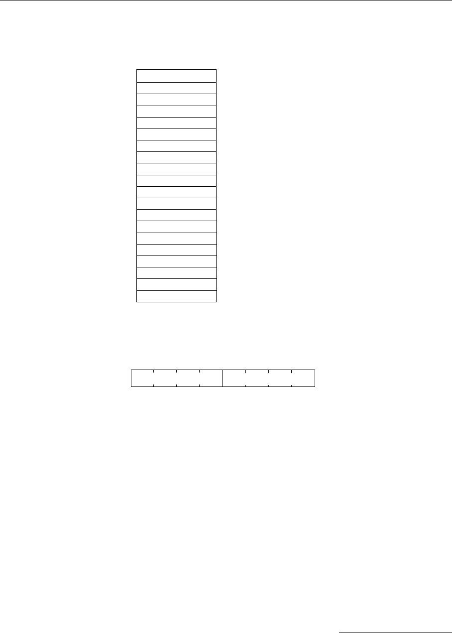
Figure 27. General flow chart of the A733 software.
Reset
Initialization
Sleep
0.5 sec
interrupt?
No
Yes
Connectivity
Check? Do Connectivity
Check
Yes
Terminal
Mode?
No
Enable Terminal
Mode
Yes
No
RF Channel
Activity? Handle Incoming
Message
Yes
No
Time to A/D
Sample?
A/D Sample
and Process Yes
Switch off
Everything
Battery
Low? Storage
Mode? Yes
No No
No
Stop
Battery
Distress?
Yes
Yes
No
0.5 sec Interrupt
Advance the
RTC one second
Return
Increment
the RTC?
Yes
No
Counter Interrupt
Debounce input
Return
Increment
affected Counter

47
Serial Communication Protocol
4.3. Controlling the Unit
The unit under test can be controlled by means of the special serial cable supplied
by Adcon Telemetry that is connected to a PC (e.g. a laptop) on one side and to the
POWER connector on the other side. In order to switch the unit to various modes of
operations, a simple communications terminal program will suffice (e.g. Terminal or
Hyperterminal in Windows, or Kermit under other platforms). The terminal program
must be configured as follows:
• 19200 Baud
• 8 Data Bits
• No Parity
• 1 Stop Bit
• Force LF after CR
Note: The interface is TTL, not RS-232. The adapter cable provided by Adcon must
be used.
4.3.1. Serial Communication Protocol
This protocol is based on a master sending commands and a node answering; the
whole communication is conducted in plain ASCII, as strings. When exchanging
numbers, they are represented in decimal format. All commands are terminated with
a CR/LF combination. All responses (answers) are terminated with the # character.
4.3.2. General Format of a Command
The commands have the following format:
ID Command Param1 Param2 ... ParamN
•ID is the destination device. If you include an ID as part of a command, the
node checks whether ID=ownID. If it does, the node executes the command
on itself. If the ID is not the node’s ID, the node executes the command on a
remote device, if such an ID exists. If the ID is missing, this implies that the
command is addressed locally.
Note: Not all the commands can be relayed remotely.
•Command is the command proper, which can be composed of a variable string
of characters (for example, SLOT). Each node can implement a set of com-
mands depending on the functionality of the node itself. However, as a mini-
mum requirement, a node recognizes the CMDS command, which returns a list
with the commands recognized by the node.
•Param1 Param2 ... ParamN
represent the parameters, which are com-
mand dependent. If you type no parameters when you issue a command, it is
the equivalent of querying for information (the GET version of a command). If

48
Software
you type parameters, you are issuing the SET version of a command and are
setting the command to the parameters you typed.
4.3.3. General Format of an Answer
The answers have the following format:
ID Command Result1 Result2 ... ResultN ErrResult
#
•ID is the answering device. If a command was further routed, it is the ID of
the end device. The answer must always contain the ID on return.
•Command is the string representing the original command. It is supplied so
that a master can distinguish between the answers it is waiting for, and out-
of-band notifications (which may come, for example, over the radio port of a
node). As with the ID, the command name must be always supplied.
•Result1 Result2 ... ResultN are the result values returned by the re-
mote node. If the ErrResult is not zero, all other possible characters and/
or strings until the end of the line may be ignored.
•ErrResult shows whether the command was successfully executed. If this
value is 0, the command was successfully executed. If this value is other than
0, the command failed. The number may further indicate the error type. (See
also “Returned errors list” on page 54.)
The answer string may contain any number of spaces or CR/LF characters between
its components; however, after the terminator (#) no other characters are allowed.
4.3.4. Commands
Both uppercase and lowercase characters can be typed because the commands are
not case sensitive. The commands list is not exhaustive, only those commands
deemed necessary for type approval testing were included.
CMDS
DESCRIPTION Returns a list of supported commands.
PARAMETERS None.
REMARKS GET only.
RETURNS A list of strings separated by spaces.
REMOTE No.
EXAMPLE CMDS
193 CMDS CMDS ID PMP RSSI TIME FREQ DEV DEL REPL SLOT DATA INFO RX TX ERA 0
#

49
Commands
TIME
DESCRIPTION Sets/returns the real time clock.
PARAMETERS The actual time, or none in the GET version.
RETURNS The actual time as dd/mm/yyyy hh:mm:ss.
REMARKS GET/SET.
REMOTE No.
EXAMPLES TIME 12/12/1999 22:10:10
193 TIME 0
#
TIME
193 TIME 12/12/1998 22:10:10 0
#
BL
DESCRIPTION Sets/returns the band limits.
PARAMETERS The frequency band limits (Hz), or none in the GET version.
RETURNS The actual frequency band limits, in Hz.
REMARKS GET/SET. This is a hidden command (i.e. not available for the normal user in the
CMDS list).
REMOTE No.
EXAMPLE BL 432000000 450000000
193 BL 0
#
BL
193 BL 432000000 450000000 0
#
FREQ
DESCRIPTION Sets/returns the operating frequency.
PARAMETERS The operating frequency and step (Hz), or none in the GET version.
RETURNS The actual frequency and step, in Hz.
REMARKS GET/SET.
REMOTE Yes, SET only.
EXAMPLE FREQ 433925000 25000
193 FREQ 0
#

50
Software
FREQ
193 FREQ 433925000 25000 0
#
DATA
DESCRIPTION Returns data stored for a certain device.
PARAMETER The ID of the device for which the data is requested and the date/time (in the stan-
dard format) the data was stored. If missing, it refers to the data of the local device.
RETURNS A data block.
REMARKS GET only. If the date/time parameter is not included, the latest data is returned. If
the date/time parameter is included, the date and time closest to, but later than, the
given date/time is returned.
REMOTE Yes, for a GET, but only one frame at a time. The A733 can issue the command only
for itself, locally.
EXAMPLE DATA 193 12/12/1998 12:12:12
193 DATA b1 b2 b3 ... bn 0
#
The data block returned will typically contain a number of data frames (telegrams).
The structure of a block is as follows:
dd mm yyyy hh mm ss si ft d1 d2 ... dn dd mm yyyy ... dn cs
where:
•dd mm yyyy is the date
•hh mm ss is the time
•si is the size of the frame (21 for frame type 37)
•ft is the frame type (37 for the A733)
•d1 d2 ... dn are the data values (the frame content)
•cs is a 16-bit checksum obtained by summing the bytes and discarding the
carries over 0xFFFF
51
Commands
The A733 devices always respond with a type 37 data frame (see also “Data12” on
page 62). The composition of the data block of such a frame (the values marked as
d1, d2... dn) is depicted in Figure 28, while the digibyte is depicted in Figure 29.
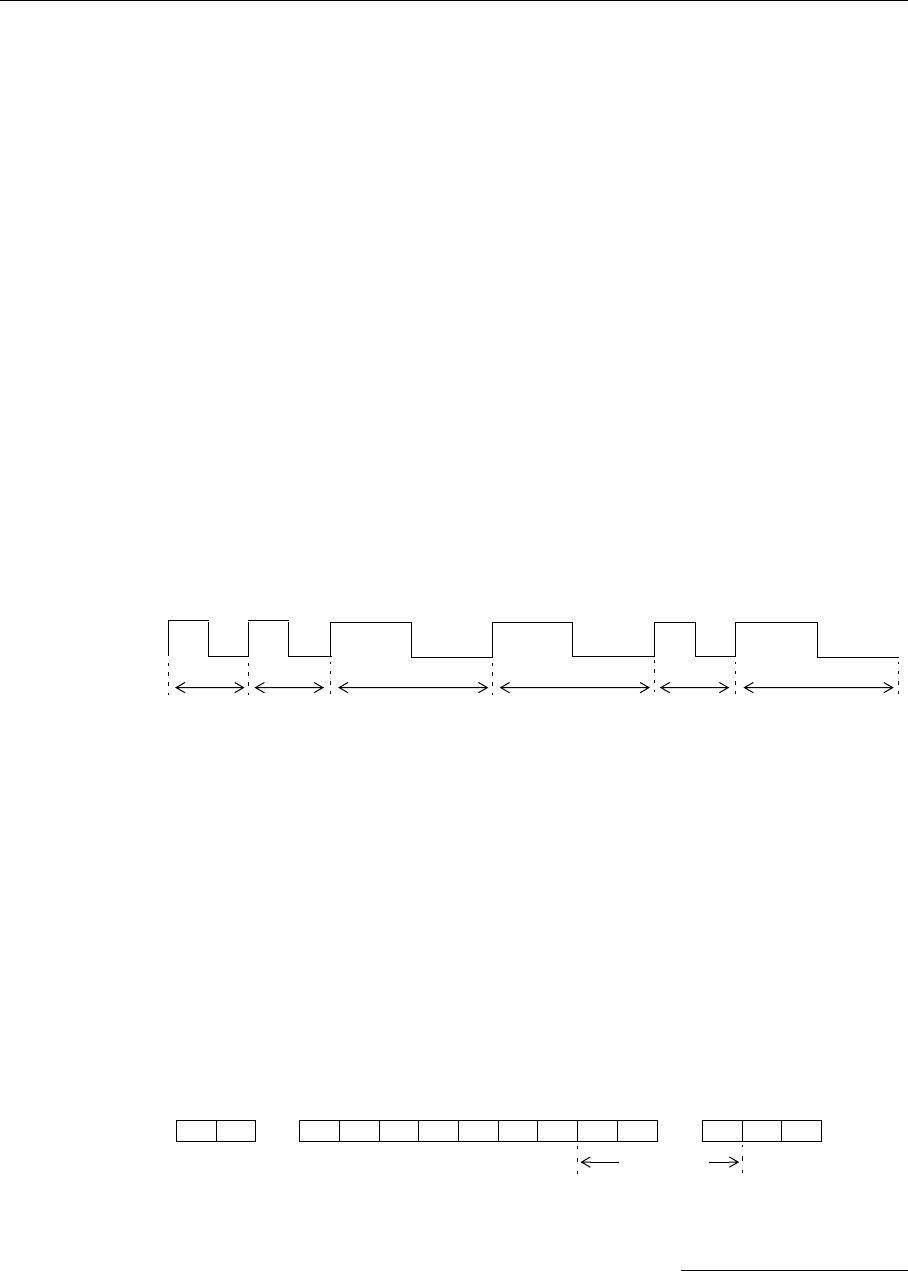
Figure 28. Frame 37 description
Figure 29. The Digibyte
The remote version is limited to a single frame. An example of such a command is
given below:
9999 DATA 9999 30/9/1999 14:50:00
9999 DATA
30 9 1999 14 54 55 21 37 255 255 77 0 0 0 0 89 156 126 20 0 0 0 0 0 0 0 0 0 3197 0
#
Notice that if you need to get data that is not the last (newest) slot remotely from a
device, the ID must be supplied twice. If you need to get the last slot stored, you
can ignore the ID and the date/time parameters:
9999 DATA
9999 DATA
13 9 1999 19 26 36 21 37 255 255 79 0 0 0 0 87 148 149 15 0 0 0 0 0 0 0 0 0 3148 0
RF incoming
RF outgoing
Digibyte
I/O A Pulse Counter
I/O B Pulse Counter
Battery
I/O A Cabling 1
I/O A Cabling 2
I/O A Cabling 3
I/O B Cabling 1
I/O B Cabling 2
I/O B Cabling 3
I/O C Pulse Counter
I/O D Pulse Counter
I/O C Cabling 1
I/O C Cabling 2
I/O C Cabling 3
I/O D Cabling 1
I/O D Cabling 2
I/O D Cabling 3
b7 b0
SC Dig 6 Dig 5 Dig 4 Dig 3 Dig 2 Dig 1 Dig 0
SC — Battery charge (0–off, 1–on) Dig n — Digital I/O n

52
Software
#
IMME
DESCRIPTION Samples all inputs and immediately returns the sampled data.
PARAMETER The ID of the requested subsystem, default is the standard A/D subsystem of the
A733 (ID=0).
Note: Currently only the default subsystem is implemented on the A733.
RETURNS A data block.
REMARKS GET only. The command needs a certain delay to execute, e.g. for the standard sub-
system this delay amounts to two seconds. The delay is necessary to allow for the
sensors to settle after applying power to them.
REMOTE No.
EXAMPLE IMME
9999 IMME
13 9 1999 19 26 36 21 37 255 255 79 0 0 0 0 87 148 149 15 0 0 0 0 0 0 0 0 0 3148 0
#
INFO
DESCRIPTION Returns various status information.
PARAMETERS None.
RETURNS A list of a device’s internal variables:
ID INFO rf_in rf_out date time ver clk stack cop batt temp days_uptime
hr:min_uptime rssi pmp_low pmp_high type slot samples err_level
#
The formats for the above parameters are as follows:
•rf_in and rf_out as a decimal (unsigned char)
•date as dd/mm/yyyy
•time as hh:mm:ss
•ver as x.x
•clk, stack, and cop as decimal (unsigned char); they represent internal
housekeeping parameters: the A733 uses cop to number watchdog occur-
rences, but clk and stack are currently undefined
•batt as battery level using the standard voltage conversion equation (0 is 0
volts, 255 is 20 volts)
•temp as internal temperature in the A733 housing, which is device depen-
dent. The precision of the sensing element is low (±2°C), but it is sufficient for

53
Commands
battery power management (charge/discharge). To compute the actual value
(in °C), the following equation must be used:
•days_uptime in days; together with hr:min_uptime, it represents the
amount of time the device is up without a reset or watchdog
•hr:min_uptime in hours:minutes format
•rssi as decimal (unsigned chars); it is the programmed value with the RSSI
command
•pmp_low and pmp_high are the programmed values with the PMP com-
mand
•type is used to represent the device type; following types are assigned cur-
rently:
— 0 for A730MD
— 1 for A720
— 2 for A730SD
— 3 for A720B
— 4 for A733
•slot and samples are the actual values programmed by means of the SLOT
command
•err_level is the error value; 0 means no error
REMARKS GET only.
REMOTE Yes, GET only. The A733 can issue the command both remotely and locally.
EXAMPLE INFO
193 INFO 255 0 18/4/1999 21:5:11 1.3 0 0 0 91 72 40 1:46 58 65 72 3 900 15 0
#
RX
DESCRIPTION Switches the unit to permanent receive mode (for tuning purposes).
PARAMETERS None.
RETURNS Nothing.
REMARKS The system stops, and exits the command only when a key is pressed. This com-
mand returns no message.
REMOTE No.
EXAMPLE RX
193 RX 0
#
Temp °C[] internalTemp 400⋅
255
------------------------------------------------- 6 8–=

54
Software
TX
DESCRIPTION Switches the unit to transmit mode (for tuning purposes).
PARAMETERS None (sends an unmodulated carrier), 1 (sends a 1 kHz modulated carrier), 0 (sends
a 2 kHz modulated carrier) or 5 (sends a mixed 1 + 2 kHz modulated carrier).
RETURNS Nothing.
REMARKS The system stops, and exits the command only when a key is pressed. This com-
mand returns no message.
REMOTE No.
EXAMPLE TX
193 TX 0
#
TX 1
193 TX 0
#
TX 5
193 TX 0
#
B
DESCRIPTION Sends a broadcast frame.
PARAMETERS None.
RETURNS A data block.
REMARKS After the device sends the broadcast frame, it will listen for answers. All valid an-
swers will be listed with their IDs.
REMOTE No.
EXAMPLE B
193 B 0
#234 BA 0
#7851 BA 0
4.3.5. Returned errors list
Following are error messages you might get.
Command line interpreter
• 1 — nonexistent command
• 2 — command line buffer overflow (input line too long)
• 3 — internal error

55
Returned errors list
• 4 — reserved
• 5 — missing or false parameters in command
• 6 — operation not implemented
Device descriptors and storage handler
• 10 — device not found (attempt to perform a command on a nonexistent de-
vice)
• 11 — device already exists
• 12 — reserved
• 13 — no more space for descriptors (too many devices)
• 14 — no more records for the specified device
• 15 — temporary communication break, no more data (the last request was not
successful)
• 16 — time-out (the handler blocked or is busy)
• 17 — internal error
• 18 — attempt to insert a reserved device ID number (0 or 65535)
Real time clock
• 20 — incorrect time supplied (no conversion to time_t was possible)
Radio interface
• 30 — error at receive (CRC, etc.)
• 31 — unexpected frame received
• 32 — wrong length
• 33 — reserved
• 34 — reserved
• 35 — time-out (remote device not responding)
• 36 — receiver busy (for example, just making the request round)
Notifications
• 40 — request to read a notification when no notification is pending
56
Software
4.4. Adcon Packet Radio Protocol
The A733 is basically intended as an end device in a radio network. Most frames de-
fined by the Adcon Packet Radio Protocol are recognized and answered by an A733;
a complete list is provided (see “Frame Types” on page 59). In addition, full source
routing of frames for other destinations is implemented.
Figure 30. State Transition Diagram of the radio communication task.
4.4.1. Digital Squelch
In order to reduce the power consumption during receive mode, the unit uses a pro-
tocol developed by Adcon Telemetry for the A730 family, but with some additional
refinements to further reduce the power consumption. The receiver is pulsed at a
0.5 seconds interval. At wake-up, the receiver samples first the RF channel for a car-
rier, by measuring the RSSI. The RSSI output is extremely stable due to the wide dy-
namic range that the IF chip exhibits (over 100 dB, temperature compensated). If the
sampled RSSI is under a preset threshold, the unit will immediately go back to sleep.
This procedure takes under 20 mS, typically (from wake-up to result).
If, however, an RF level superior to the preset threshold is detected, the micropro-
cessor will try to detect a valid header, which is composed of a 2 kHz tone of at least
0.5 seconds long. The tone detection is performed by the microcontroller in soft-
Idle
Measure RF
Check
Destination
No Signal
0.5 sec
Interrupt
Header Detected
Not for us
Get Frame
We are called
New Frame Possible
Wait
Nhops + 1 s
and
Hunt Syncs
Timeout Expired
Answer
Appropriately
Ack
Resend
Frame with
Long
Header
Frame Sent Twice
No Ack
Payload is for us
Must route
Update
Header
and Send
Ack
No Ack
57
Modulation Technique Used
ware, and takes at most 6 additional milliseconds. If no valid tone is detected, the
unit goes back to sleep, otherwise it tries to decode the frame.
Based on the destination ID, the frame will be identified. If it is not for that particular
unit (own ID), then the microcontroller will cease decoding it and will go immediately
to sleep. The destination ID is positioned very early in the frame header (see also
“Generic Format of a Radio Frame” on page 57).
From the above it becomes clear that in order to initiate a communication, a re-
quester must send first a header which is at least 0.5 seconds long: these are called
long header frames
. Of course, after the communication is established the headers
are short, of only 16 bytes (i.e. 8 msec. – called
short header frames
). If a timeout
occurs, the system will restart by sending long header frames.
4.4.2. Modulation Technique Used
The communication via radio is made by using a special MSK (Minimum Shift Keying)
scheme; both the encoding and the decoding of the MSK frames is made in soft-
ware—there is virtually no hardware modem. A
zero
bit is transmitted as a sequence
of 250 µs one level followed by a 250 µs zero level, while a
one
bit is transmitted as
a 500 µs one level followed by a 500 µs zero level. A complete sequence of one and
zero level forms a
bit cell
.
This modulation scheme is self-clocked. The transmission speed is content-depen-
dent, varying from 1 kbps (when sending only ones) to 2 kbps (when sending only
zeros). On the average, an 1500 bps transmission speed is reached.
The data interchange between stations is made by means of
frames
. The frames
have a header, a 16 bit-sync character, a data block, and a 16-bit CRC number. The
bytes forming the frame are send synchronously, with no start and/or stop bits. The
data block is assembled after the sync character was detected. The LSB of a byte is
sent first and the MSB is sent last.
4.4.3. Generic Format of a Radio Frame
The standard frame format used by the A730 family is as follows:
00 0
111
00 00 ....... 00 0xAA DST-H DST-L SRC-H SRC-L DLEN .......
DATA1 DATA2 DATAn CRC-H CRC-L
Data Frame

58
Software
• The frame starts with a header of zeros and there are two header types: long
and short. The long headers are used to wake up a remote station and must
be 140 bytes long, while the short headers are only 16 bytes long.
• After the header, a synchronization character is used; this is a hex 0xAA byte.
The implementation must ensure that a 16-bit sync character is checked, i.e.
0x00AA, and not only an 8-bit 0xAA character.
• Following the synchronization pattern, the bytes are assembled by shifting
the bits one by one: each 8 contiguous bits will be “cut” into a byte. First in-
formation assembled is the destination (DST) address: this is in order for all
the receiving stations to know if they must assemble the whole frame, or they
can go back to sleep. Only the addressed station will remain active after this
information was decoded.
Note: The byte ordering convention used on the network is “big endian,” i.e. the
MSB is sent first and the LSB last.
• Next are the source (SRC) address and the length of the data field. The data
field follows, and the frame is ended by a 16-bit CRC field. The CRC is com-
puted starting with the first byte after the SYNC character until (but not in-
cluding) the CRC bytes.
The data field can transport various type of data frames. After being successfully de-
coded and checked, these data frames are passed to the upper layer of the soft-
ware. The data frames recognized by the A733 and their answers are detailed in
“Data Frames” on page 59.
A device will answer to the requesting device with the answer frame. The answering
device will poll the radio channel for an acknowledge; the acknowledge may be ei-
ther the same frame send further up the network (if the communication has hops, i.e.
routing stations in between the master and remote device), or an acknowledge send
by the master – the master sends only a short radio frame containing the SRC and
DST, both being its own ID. If the answering device does not receive the acknowl-
edge, it will repeat the frame after a one second delay (only once).
Another notable feature of the system is the way it handles the long and short head-
er frames. When a frame is sent by the master for the first time, it will be one with a
long header; all the stations on the path of the frame participating in a certain trans-
action will relay the frame with a long header. After relaying the frame, the stations
will remain active for a time calculated as (in seconds):
The above scheme assures that as long as another frame will follow during this time
interval (addressed to a station that is known to be also active), the header sent to
that station will be a short one.
Delay Hops 1+=

59
Data Frames
4.4.4. Data Frames
The data frames (payload) are the blocks of data extracted from the radio frames,
after the CRC and other information (source address) was checked. The data frame
and its length are passed to the upper layers of the software.
Figure 31. Generic Data Frame structure.
A data frame is composed of two main parts: a header, containing the frame type as
well as the routing information, and a data block. The length of the data block can
be easily computed by subtracting the header length (HLEN + 1 byte for the TYPE)
from the original data frame length received from the lower layer of the software (the
radio frame length). Additional explanations on the notation used in the diagram:
•TYPE is the type of frame; the types recognized and/or used by the A733 will
be detailed individually later in this chapter (see “Frame Types.”)
•HLEN is the header length: it represents the number of bytes used to de-
scribe the route the frame will go (or went). The maximum number of hops is
8, that is, 8 intermediate stations plus source and destination. Each station is
described by its unique 16-bit address.
•SRC, HOP and DEST, are the source, the hops and the destination addresses.
While the hops may be missing (no routing stations between source and des-
tination), the source and destination are mandatory.
•DATA is the data proper field. It is limited in length, its maximum size being
dependent also on the particular route: if the route is longer (8 hops) then the
data block is limited to 48 bytes. Depending on the frame type, the data block
may be nonexistent (zero length).
4.4.5. Frame Types
Although the original Adcon Packet Radio Protocol contains many frame types, only
those relevant to the A733 are presented here.
Request
ID 1
FORMAT struct {
time_t init_time;
time_t req_time;
} request;
DESCRIPTION The Request frame is used by a master to request data frames from a remote station.
A remote will answer with a data frame. There are currently three types of data
TYPE HLEN SRC-H SRC-L .......
HOP1-H HOP1-L HOPn-H HOPn-L DEST-LDEST-H DATA1 DATA2 DATAn
.......
Header (Frame Type + Routing Information) Data

60
Software
frames: normal (type 8), extended (type 37), and reduced (type 38); the A733 an-
swers with the extended type (see also “Data12” on page 62).
•init_time represents the actual time to be used by the remote to re-initialize
its local RTC; if its value is time_t NULL (default), then no re-initialization will
be performed.
•req_time is the time for requested data. An A733 will search its internal data
buffer for data that has a time stamp that is strictly newer than req_time.
Therefore, if a master requests data with exactly the time stamp previously
supplied by the remote, the remote must deliver a newer data slot. If the re-
quested data is too old, the remote will send its oldest data, while if the re-
quested data is too new, the remote will answer with the newest data it has.
If the device is not yet initialized and has no data (i.e. its internal time is 1/1/
1970), then it will send a Data12 frame with no relevant data, but with the time
stamp of 1/1/1970. This mechanism will inform a master that the device needs
initialization.
On the A733 this command can be initiated by means of the DATA command (see
also “DATA” on page 50).
SEE ALSO Data12 frame.
Broadcast Answer
ID 2
FORMAT struct {
unsigned char RF_levelOut;
} broadcast_answer;
DESCRIPTION This is the answer to a broadcast request frame; the RF_levelOut is the level record-
ed by the device when receiving the broadcast request frame. The A733 will receive
and interpret such frames depending on the mode it was in when it issued the
broadcast request (see also “Broadcast Request” on page 60). In terminal mode, all
the broadcast answers will be displayed with their RF levels, while in connectivity
check mode, the LED tool will be activated. The device will pulse the LED tool for
the number of answers it identified.
If the A733 receives a Broadcast request, it must answer to it, but in a random man-
ner. An 8 seconds time interval starting with the end of the Broadcast request frame
is divided in 16 slots, each 0.5 seconds long. The A733 must select randomly one of
these 16 slots for sending its answer. This frame, as well as the Broadcast request
frame, is not routable.
SEE ALSO Broadcast Request frame.
Broadcast Request
ID 6
FORMAT The data frame body is empty.

61
Frame Types
DESCRIPTION This frame is sent by the device when the LED tool is inserted in the POWER con-
nector, or if the command B is issued in terminal mode. This frame is special in that
the destination address (DST) in the header is 0. This type of frame is not routable.
All devices having received this frame must reply in a random fashion with a Broad-
cast answer frame.
SEE ALSO Broadcast Answer frame.
Ping
ID 9
FORMAT The data frame body is empty.
DESCRIPTION This frame is used to request an answer from a device; it is used to check if the de-
vice is available and reports on various conditions of the remote. The addressed de-
vice must answer with a Pong frame. On an A733, this command can be initiated
from the terminal by means of the INFO command (see also “INFO” on page 52).
SEE ALSO Pong frame.
Pong
ID 10
FORMAT struct {
unsigned char RF_levelIn;
unsigned char RF_levelOut;
time_t RTC;
unsigned char version;
unsigned char clkfail;
unsigned char stackfail;
unsigned char WDT;
unsigned char batt;
unsigned char internalTemp;
time_t uptime;
unsigned char rssi;
unsigned char pmp_low;
unsigned char pmp_high;
unsigned char type;
unsigned int slot;
unsigned char samples;
} pong;
DESCRIPTION The Pong frame is an answer to the Ping frame. In addition to informing a caller that
a remote is active, it carries some useful information about the device’s status:
•RF_levelIn is the left zero (it is a placeholder and will be filled by the first de-
vice receiving the frame).
•RF_levelOut is the RF level measured by the device when receiving the Ping
frame.
•RTC is the actual value of the remote’s Real Time Clock.

62
Software
•version is the software/hardware version of the device.
•clkfail and stackfail are meaningless for an A733; they are kept for histor-
ical reasons.
•WDT is a counter incremented each time the device was reset due to a Watch-
dog timeout; its value is cleared at power-on reset.
•batt is the battery voltage (this value will be also found in the Data frame).
•internalTemp is the temperature in the A733 housing; the precision of the
sensing element is vry low (±2C°), but it is sufficient for battery power man-
agement (charge/discharge). To compute the actual value (in C°), the follow-
ing equation must be used:
•uptime is the time elapsed since the last reset (including a Watchdog reset).
•rssi is the programmed RSSI threshold value.
•pmp_low and pmp_high are the programmed power management parameters.
•
type
is the type of the device (will return always 4 – for A733).
Note: Some of the values described above are specific to the A733. The implemen-
tation of the Pong frame, as well as its length (number of bytes), may vary
from one device type to another.
SEE ALSO Ping frame.
Fdev
ID 32
FORMAT The data frame body is empty.
DESCRIPTION This frame requests that a remote clear its data memory (format). The remote will
answer with a General acknowledge frame. An A733 will never issue this frame type,
but it will execute and answer it.
SEE ALSO General Acknowledge frame.
Data12
ID 37
FORMAT struct {
unsigned char RF_levelIn;
unsigned char RF_levelOut;
time_t slot_timeStamp;
unsigned char digibyte;
unsigned int counter0; /* Pulse Counter I/O A input */
unsigned int counter1; /* Pulse Counter I/O B input */
unsigned int counter2; /* Pulse Counter I/O C input */
Temp °C[] internalTemp 400⋅
255
------------------------------------------------- 6 8–=
63
Frame Types
unsigned int counter3; /* Pulse Counter I/O D input */
unsigned char battery;
unsigned int analog_data[9];
} data_frame;
DESCRIPTION This frame will be sent back by the device as an answer to the Request frame.
•RF_levelIn is the left zero (it is a placeholder and will be filled by the first de-
vice receiving the frame).
•RF_levelOut is the RF level measured by the device on the Request frame.
•slot_timeStamp is the actual time stamp on the data sent.
•digibyte represents the result of OR-ing the following bits:
— SC represents the battery charge switch’ status.
— DIG0 to DIG7 are the I/O pins on the I/O connectors. Note that only the
first 4 DIGs are usable (there are only four I/O connectors on the A733).
Note: For additional info on the bits in the digibyte, check the hardware section of
this manual.
•counter0 to counter3 are the values of the pulse counters.
•battery is the value of the main power supply; its actual value can be com-
puted using the equation:
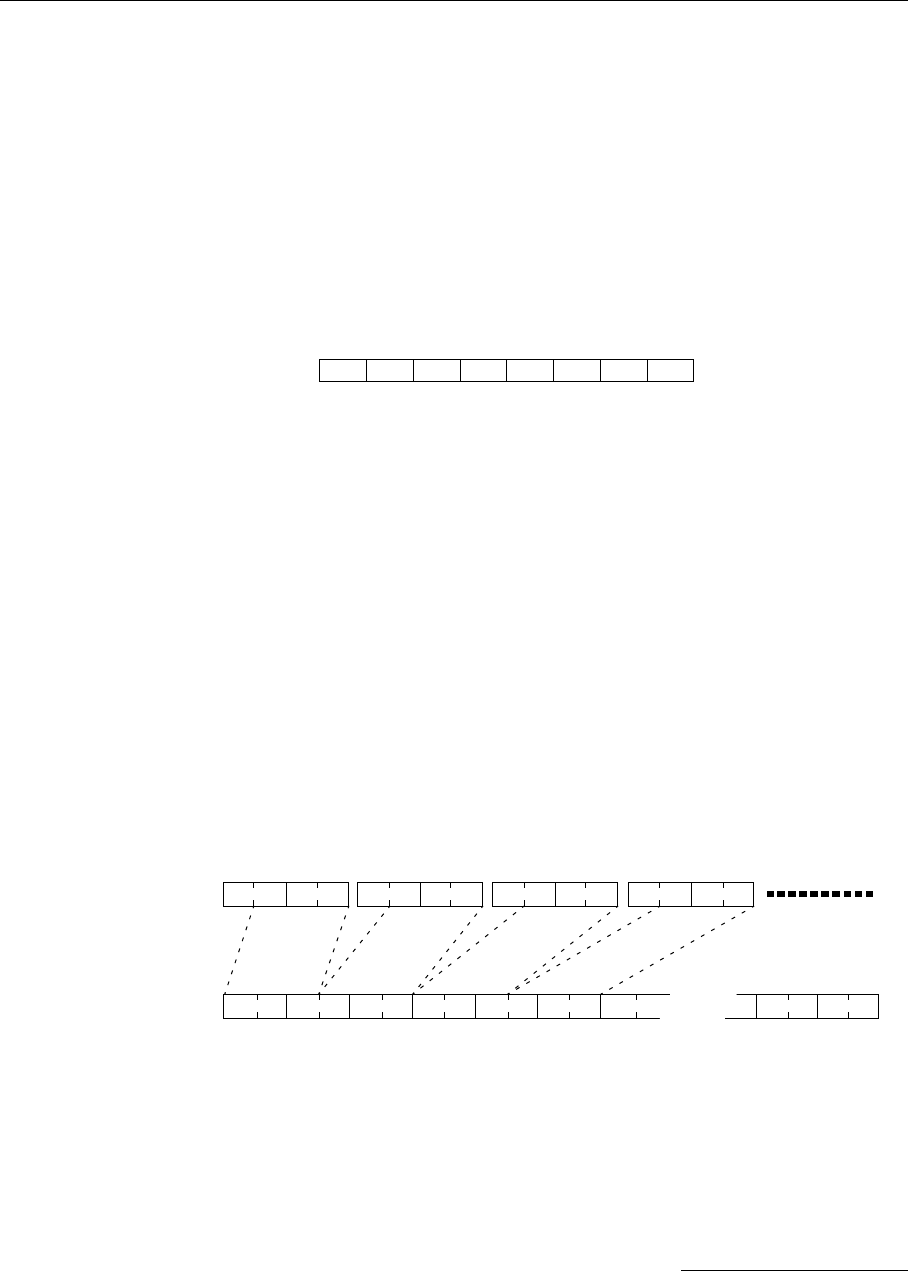
•analog_data[9] is an array of 8 unisgned integers that represents the result of
packing the 12 12-bit values. These are the values returned by the internal
A/D converter from the respective I/O connectors (see the hardware section
for more details). The packing mechanism is depicted below:
SEE ALSO Request frame.
Set ID
ID 40
SC Dig6 Dig5 Dig4 Dig3 Dig2 Dig1 Dig0
b0
b7
Batt V[] battery 20×
255
-------------------------------=
16 bit values
8 bit packed values
Integer 0 Integer 1 Integer 2 Integer 3
12 bits 12 bits 12 bits 12 bits
Byte 0 Byte 1 Byte 2 Byte 3 Byte 6Byte 5Byte 4 Byte 16 Byte 17

64
Software
FORMAT struct {
unsigned int ID;
} setId;
DESCRIPTION This frame requests a remote to change its own ID number. The remote will answer
with a General acknowledge frame
before
changing its ID. An A733 will never issue
this frame type, but it will answer to it.
SEE ALSO General Acknowledge frame.
Set Slot Time and Sample Rate
ID 41
FORMAT struct {
unsigned int slot;
unsigned char rate;
} setSlot;
DESCRIPTION This frame requests that a remote change the size of its slot (default 900 seconds,
i.e. 15 minutes) and the sampling rate (default 15).
•slot is the number of seconds a new slot of sampled and averaged data will
be stored in the internal FIFO memory of the device.
•rate is the number of samples per slot taken; these samples will be averaged
before being stored.
The remote will answer with a General acknowledge frame. An A733 will never issue
this frame type, but it will answer to it.
SEE ALSO General Acknowledge frame.
Set Frequency
ID 42
FORMAT struct {
unsigned long frequency;
unsigned int step;
} setFreq;
DESCRIPTION This frame requests that a remote change its frequency. The remote will answer with
a General acknowledge frame
before
changing its operating frequency. To further
secure the transaction, the frequency change will be performed only after the re-
mote receives the acknowledge frame from its next neighbor (for more details, see
also “Generic Format of a Radio Frame” on page 57). An A733 will never issue this
frame type, but it will answer to it.
SEE ALSO General Acknowledge frame.

65
Frame Types
Set Battery Charge Levels
ID 43
FORMAT struct {
unsigned char chargeStart;
unsigned char chargeStop;
} setBattCharge;
DESCRIPTION This frame requests that a remote change the battery charge management param-
eters. The device will answer with a General acknowledge frame. An A733 will never
issue this frame type, but it will answer to it.
•chargeStart is the value where the external power (normally a solar panel) will
be enabled to charge the battery.
•chargeStop is the value where the external power will be switched off.
From the above two values, the system will compute all other limits (e.g. misery, bat-
tery low, etc.).
SEE ALSO General Acknowledge frame.
General Acknowledge
ID 127
FORMAT struct {
int result;
} generalAck;
DESCRIPTION This frame is sent as an acknowledge to various
Set
type of frames. The result field
is NULL if the request was successfully performed; in case of failure, this field may
contain information about the cause of the failure. Its value will depend on the type
of the request.