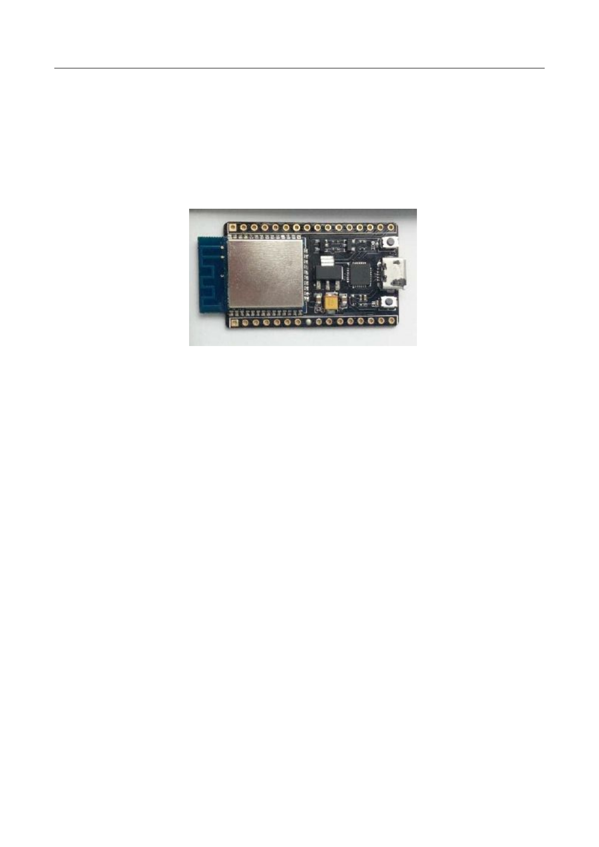
Ai Thinker Technology ESP32S Wi-Fi & Bluetooth Module User Manual ESP 32S
Shenzhen Ai-Thinker Technology co., LTD Wi-Fi & Bluetooth Module ESP 32S
Contents
- 1. Users Manual
- 2. User manual
Users Manual
ESP-32S User Manual
ESP-32S User Manual
REV 1.0
2017.3

ESP-32S User Manual
FCC STATEMENT
This device complies with Part 15 of the FCC Rules. Operation is subject to the following two conditions:
(1) This device may not cause harmful interference.
(2) This device must accept any interference received, including interference that may cause undesired
operation.
Any changes or modifications not expressly approved by the party responsible for compliance could void the
user’s authority to operate the equipment.
Please notice that if the FCC identification number is not visible when the module is installed inside another
device, then the outside of the device into which the module is installed must also display a label referring to
the enclosed module. This exterior label can use wording such as the following: “Contains FCC ID:
2AHMR-ESP32S” any similar wording that expresses the same meaning may be used.
This equipment complies with FCC radiation exposure limits set forth for an uncontrolled environment. This
equipment should be installed and operated with a minimum distance of 20cmbetween the radiator & your
body. This transmitter must not be co-located or operating in conjunction with any other antenna or
transmitter.
The module is limited to OEM installation ONLY.
The OEM integrator is responsible for ensuring that the end-user has no manual instruction to remove or
install module.
The module is limited to installation in mobile application;
A separate approval is required for all other operating configurations, including portable configurations with
respect to Part 2.1093 and difference antenna configurations.
There is requirement that the grantee provide guidance to the host manufacturer for compliance with Part
15B requirements.
Copyright © 2017 Ai-Thinker Technology Co., Ltd. All rights reserved.

ESP-32S User Manual
Contents
1.Preface................................................................................................................................................ 1
2. Pin Definitions....................................................................................................................................3
2.1 Pin Layout................................................................................................................................. 3
2.2 Pin Description......................................................................................................................... 4
2.3 Strapping Pins...........................................................................................................................5
3. Functional Description.......................................................................................................................7
3.1 CPU and Internal Memory........................................................................................................7
3.2 External Flash and SRAM..........................................................................................................7
3.3 Crystal Oscillators..................................................................................................................... 7
3.4 Power Consumption.................................................................................................................8
3.5 Peripherals and Sensors........................................................................................................... 9
3.5.1 Peripherals and Sensors Description.............................................................................9
3.5.2 Peripheral Schematics................................................................................................. 14
4. Electrical Characteristics..................................................................................................................15
4.1 Absolute Maximum Ratings................................................................................................... 15
4.2 Recommended Operating Conditions....................................................................................15
4.3 Digital Terminal Characteristics............................................................................................. 15
4.4 Wi-Fi Radio............................................................................................................................. 16
4.5 Bluetooth LE Radio................................................................................................................. 16
4.5.1 Receiver....................................................................................................................... 16
4.5.2 Transmit...................................................................................................................... 17
4.6 Reflow Profile......................................................................................................................... 17
5. Schematics....................................................................................................................................... 18

ESP-32S User Manual
Shenzhen Ai-Thinker Technology Co., Ltd http://www.ai-thinker.com
1.Preface
ESP-32S is a powerful, generic Wi-Fi +BT+BLE MCU module that targets a wide variety of applications,
ranging from low-power sensor networks to the most demanding tasks, such as voice encoding, music
streaming and MP3 decoding.
At the core of this module is the ESP32-D0WDQ6 chip*, which is designed to be scalable and adaptive. There
are two CPU cores that can be individually controlled or powered, and the clock frequency is adjustable from
80 MHz to 240 MHz . The user may also power off the CPU and make use of the low-power coprocessor to
constantly monitor the peripherals for changes or crossing of thresholds. ESP32 integrates a rich set of
peripherals, ranging from capacitive touch sensors, Hall sensors, low-noise sense amplifiers, SD card
interface, Ethernet, high speed SDIO/SPI, UART, I2S and I2C.
The integration of Bluetooth, Bluetooth LE and Wi-Fi ensures that a wide range of applications can be
targeted, and that the module is future proof: using Wi-Fi allows a large physical range and direct connection
to the internet through a Wi-Fi router, while using Bluetooth allows the user to conveniently connect to the
phone or broadcast low energy beacons for its detection. The sleep current of the ESP32 chip is less than 5
µA, making it suitable for battery powered and wearable electronics applications. ESP-32S supports data
rates of up to 150 Mbps, and 22 dBm output power at the PA to ensure the widest physical range. As such
the chip does offer industry-leading specifications and the best performance for electronic integration, range,
power consumption, and connectivity.
The operating system chosen for ESP32 is free RTOS with LWIP; TLS 1.2 with hardware acceleration is built in
as well. Secure (encrypted) over the air (OTA) upgrade is also supported, so that developers can continually
upgrade their products even after their release.
Table 1 provides the specifications of ESP-32S.
Table 1: ESP-32S Specifications
Categories
Items
Specifications
Wi-Fi
Standards
FCC/CE/IC/TELEC/KCC/SRRC/NCC
Protocols
802.11 b/g/n/d/e/i/k/r (802.11n up to 150 Mbps)
A-MPDU and A-MSDU aggregation and 0.4 µs guard
interval support
Frequency range
2.4 〜2.5 GHz
Bluetooth
Protocols
Bluetooth v4.2 BR/EDR and BLE specification
Radio
NZIF receiver with -98 dBm sensitivity
Class-1, class-2 and class-3 transmitter
AFH
Audio
CVSD and SBC

ESP-32S User Manual
Shenzhen Ai-Thinker Technology Co., Ltd http://www.ai-thinker.com
Categories
Items
Specifications
Hardware
Module interface
SD card, UART, SPI, SDIO, I2C, LED PWM, Motor PWM,
I2S, I2C, IR
GPIO, capacitive touch sensor, ADC, DAC, LNA pre-
amplier
On-chip sensor
Hall sensor, temperature sensor
On-board clock
40 MHz crystal
Operating voltage
2.2 〜3.6V
Operating current
Average: 80 mA
Operating temperature range
-40°C ~ 85°C *
Ambient temperature range
Normal temperature
Package size
18 mm x 25.5 mm x 2.8 mm
Software
Wi-Fi mode
Station/SoftAP/SoftAP+Station/P2P
Security
WPA/WPA2/WPA2-Enterprise/WPS
Encryption
AES/RSA/ECC/SHA
Firmware upgrade
UART Download / OTA (via network) / download and
write firmware via host
Software development
Supports Cloud Server Development / SDK for custom
firmware development
Network protocols
IPv4, IPv6, SSL, TCP/UDP/HTTP/FTP/MQTT
User configuration
AT instruction set, cloud server, Android/iOS app
ESP-32S User Manual
Shenzhen Ai-Thinker Technology Co., Ltd http://www.ai-thinker.com
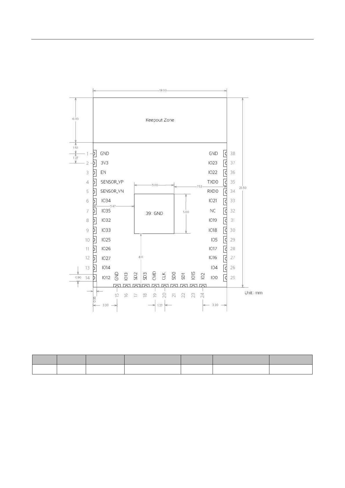
2. Pin Definitions
2.1 Pin Layout
Figure 1: Top and Side View of ESP-32S
Table 2: ESP-32S Dimensions
Length
Width
Height
PAD size (bottom)
Pin pitch
Shielding can height
PCBthickness
18 mm
25.5 mm
2.8± 0.1 mm
0.85 mm x 0.9 mm
1.27 mm
2 mm
±0.1mm

ESP-32S User Manual
Shenzhen Ai-Thinker Technology Co., Ltd http://www.ai-thinker.com
2.2 Pin Description
ESP -32S has 39 pins. See pin definitions in Table 3.
Table 3: ESP-32S Pin Definitions
Name
No.
Type
Function
GND
1
P
Ground
3V3
2
P
Power supply.
EN
3
I
Chip-enable signal. Active high.
SENSOR_VP
4
I
GPI036, SENS0R_VP, ADC_H, ADC1_CH0, RTC_GPI00
SENSOR_VN
5
I
GPI039, SENS0R_VN, ADC1_CH3, ADC_H, RTC_GPI03
IO34
6
I
GPI034, ADC1_CH6, RTC_GPI04
IO35
7
I
GPI035, ADC1_CH7, RTC_GPI05
IO32
8
I/O
GPI032, XTAL_32K_P (32.768 kHz crystal oscillator input), ADC1_CH4,
T0UCH9, RTC_GPI09
IO33
9
I/O
GPI033, XTAL_32K_N (32.768 kHz crystal oscillator output), ADC1_CH5,
T0UCH8, RTC_GPI08
IO25
10
I/O
GPI025, DAC_1, ADC2_CH8, RTC_GPI06, EMAC_RXD0
IO26
11
I/O
GPI026, DAC_2, ADC2_CH9, RTC_GPI07, EMAC_RXD1
IO27
12
I/O
GPI027, ADC2_CH7, T0UCH7, RTC_GPI017, EMAC_RX_DV
IO14
13
I/O
GPraM,ADC2_CH6, T0UCH6,MTMS, HSPHK,HS2_CLK, SD_CLK,
EMAC_TXD2
IO12
14
I/O
GPI012, ADC2_CH5, T0UCH5, RTC_GPI015, MTDL HSPIQ, HS2_DATA2,
SD_DATA2, EMAC_TXD3
GND
15
P
Ground
IO13
16
I/O
GPI013, ADC2_CH4, T0UCH4, RTC_GPI014, MTCK, HSPID, HS2_DATA3,
SD_DATA3, EMAC_RX_ER
SHD/SD2*
17
I/O
GPIO9, SD_DATA2, SPIHD, HS1_DATA2, U1RXD
SWP/SD3*
18
I/O
GPIO10, SD_DATA3, SPIWP, HS1_DATA3, U1TXD
SCS/CMD*
19
I/O
GPIO11, SD_CMD, SPICSO, HS1_CMD, U1RTS
SCK/CLK*
20
I/O
GPIO6, SD_CLK, SPICLK, HS1_CLK, U1CTS
SDO/SD0*
21
I/O
GPIO7, SD_DATA0, SPIQ, HS1_DATA0, U2RTS
SDI/SD1*
22
I/O
GPIO8, SD_DATA1, SPID, HS1_DATA1, U2CTS
IO 15
23
I/O
GPIO15, ADC2_CH3, T0UCH3, MTD0, HSPICSO, RTC_GPI013, HS2_CMD,
SD_CMD, EMAC_RXD3
IO 2
24
I/O
GPIO2, ADC2_CH2, T0UCH2,HSPIWP, HS2_DATA0, SD_DATA0
IO 0
25
I/O
GPIO0, ADC2_CH1, T0UCH1, CLK_0UT1, EMAC_TX_CLK
IO 4
26
I/O
GPIO4,ADC2_CH0,T0UCH0, RTC_GPI010, HSPIHD, HS2_DATA1,
SD_DATA1, EMAC_TX_ER
IO 16
27
I/O
GPIO16, HS1_DATA4, U2RXD, EMAC_CLK_0UT
IO 17
28
I/O
GPIO17, HS1_DATA5, U2TXD, EMAC_CLK_0UT_180
IO 5
29
I/O
GPIO5, VSPICSO, HS1_DATA6, EMAC_RX_CLK
IO18
30
I/O
GPIO18, VSPHK,HS1_DATA7
IO19
31
I/O
GPIO19, VSPIQ, UOCTS, EMAC—TXDO
ESP-32S User Manual
Shenzhen Ai-Thinker Technology Co., Ltd http://www.ai-thinker.com
Name
No.
Type
Function
NC
32
-
-
IO21
33
I/O
GPIO21, VSPIHD, EMAC_TX_EN
RXD0
34
I/O
GPIO3, U0RXD, CLK_OUT2
TXD0
35
I/O
GPIO1, U0TXD, CLK_OUT3, EMAC_RXD2
IO22
36
I/O
GPIO22, VSPIWP,U0RTS, EMAC_TXD1
IO23
37
I/O
GPIO23, VSPID, HS1_STROBE
GND
38
P
Ground
GND
39
P
Ground
2.3 Strapping Pins
ESP32-D0WDQ6 has five strapping pins. Software can read the value of these five bits from the register
”GPIO_STRAPPING”. During the chip power-on reset, the latches of the strapping pins sample the voltage
level as strapping bits of ”0” or ”1”,and hold these bits until the chip is powered down or shut down.
Each strapping pin is connected with its internal pull-up/pull-down during the chip reset. Consequently, if a
strap-ping pin is unconnected or the connected external circuit is high-impedance, the internal weak
pull-up/pull-down will determine the default input level of the strapping pins.
To change the strapping bit values, users can apply the external pull-down/pull-up resistances, or apply the
host MCU5s GPIOs to control the voltage level of these pins when powering ESP32 on.
After reset, the strapping pins work as the normal functions pins.
Refer to Table 4 for detailed boot modes of configuration by strapping pins.
Table 4: Strapping Pins
Voltage of Internal LDO (VDD_SDIO)
Pin
Default
3.3V
1.8V
MTDI
Pull-down
0
1
Booting Mode
Pin
Default
SPI Flash Boot
Download Boot
GPIO0
Pull-up
1
0
GPIO2
Pull-down
Don’t-care
0
Debugging Log on U0TXD During Booting
Pin
Default
U0TXD Toggling
U0TXD Silent
MTDO
Pull-up
1
0
Timing of SDIO Slave
Pin
Default
Falling-edge Input
Falling-edge Output
Falling-edge Input
Rising-edge Output
Rising-edge Input
Falling-edge Output
Rising-edge Input
Rising-edge Output
MTDO
Pull-up
0
0
1
1
GPIO5
Pull-up
0
1
0
1
Note:
* Pins SCK/CLK,SDO/SD0, SDI/SD1, SHD/SD2, SWP/SD3 and SCS/CMD, namely, GPIO6 to GPIO11 are
connected to the integrated SPI flash integrated on ESP-32S and are not recommended for other uses.

ESP-32S User Manual
Shenzhen Ai-Thinker Technology Co., Ltd http://www.ai-thinker.com
Note:
Firmware can configure register bits to change the settings of ”Voltage of Internal LDO(VDD_SDIO)”
and ”Timing of SDIO Slave” after booting.

ESP-32S User Manual
Shenzhen Ai-Thinker Technology Co., Ltd http://www.ai-thinker.com
3. Functional Description
This chapter describes the modules and functions integrated in ESP-32S.
3.1 CPU and Internal Memory
ESP32-DOWDQ6 contains two low-power Xtensa® 32-bit LX6 microprocessors. The internal memory
includes:
•448 KB of ROM for booting and core functions.
•520 KB of on-chip SRAM for data and instruction.
•8KB of SRAM in RTC, which is called RTC SLOW Memory and can be accessed by the co-processor during
the Deep-sleep mode.
•8 KB of SRAM in RTC, which is called RTC FAST Memory and can be used for data storage; it is accessed
by the main CPU during RTC Boot from the Deep-sleep mode.
•1 kbit of eFuse, of which 256 bits are used for the system (MAC address and chip configuration) and the
remaining 768 bits are reserved for customer applications, including Flash-Encryption and Chip-ID.
3.2 External Flash and SRAM
ESP32-DOWDQ6 supports up to four 16-MB external QSPI flash and SRAM with hardware encryption based
on AES to protect developer’s programs and data.
ESP32 can access the external QSPI flash and SRAM through high-speed caches.
•Up to 16 MB of external flash are memory-mapped onto the CPU code space, supporting 8, 16 and
32-bit access. Code execution is supported.
•Up to 8 MB of external flash/SRAM are memory-mapped onto the CPU data space, supporting 8, 16 and
32-bit access. Data-read is supported on the flash and SRAM. Data-write is supported on the SRAM.
ESP-32S integrates 4 MB of external SPI flash. The 4-MB SPI flash can be memory-mapped onto the CPU code
space, supporting 8, 16 and 32-bit access. Code execution is supported. The integrated SPI flash is connected
to GPIO6, GPIO7, GPIO8, GPIO9, GPIO10 and GPIO11. These six pins cannot be used as regular GPIO.
3.3 Crystal Oscillators
The frequencies of the main crystal oscillator supported include 40 MHz, 26 MHz and 24 MHz. The accuracy
of crystal oscillators applied should be ±10PPM,and the operating temperature ranges from-40°C to 85°C.
When using the downloading tools, remember to select the right crystal oscillator type. In circuit design,
capacitors C1 and C2 that connect to the earth are added to the input and output terminals of the crystal
oscillator, respectively. The values of the two capacitors can be flexible, ranging from 6 pF to 22 pF. However,
the specific capacitive values of C1 and C2 depend on further tests and adjustments of the overall
performance of the whole circuit. Normally, the capacitive values ofC1 and C2 are within 10 pF when the
crystal oscillator frequency is 26 MHz, or 10 pF<C1 and C2<22 pF when the crystal oscillator frequency is 40
MHz.
The frequency of the RTC crystal oscillator is typically 32 kHz or 32.768 kHz. The accuracy can be out of the
range of ±20 PPM, when the internal calibration is applied to correct the frequency offset. When the chip

ESP-32S User Manual
Shenzhen Ai-Thinker Technology Co., Ltd http://www.ai-thinker.com
operates in low-power modes, the application chooses the external low-speed (32 kHz) crystal clock, rather
than the internal RC oscillators, to achieve the accurate wakeup time.
3.4 Power Consumption
With the advanced power management technology, ESP32-D0WDQ6 can switch between different power
modes as follows:
•Power mode
- Active mode: chip radio is powered on. The chip can receive, transmit, or listen.
- Modem-sleep mode: the CPU is operational and the clock is configurable. Wi-Fi / Bluetooth
baseband and radio are disabled.
- Light-sleep mode: the CPU is paused. The RTC and ULP-coprocessor are running. Any wake-up
events (MAC, host, RTC timer, or external interrupts) will wake up the chip.
- Deep-sleep mode: Only RTC is powered on. Wi-Fi and Bluetooth connection data are stored in RTC
memory. The ULP-coprocessor can work.
- Hibernation mode: The internal 8MHz oscillator and ULP-coprocessor are disabled. The RTC
recovery memory is powered down. Only one RTC timer on the slow clock and some RTC GPIOs are
active. The RTC timer or the RTC GPIOs can wake up the chip from the Hibernation mode.
•Sleep Pattern
- Association sleep pattern: The power mode switches between the active mode and
Modem-sleep/Light- sleep mode during this sleep pattern. The CPU, Wi-Fi, Bluetooth, and radio
wake up at pre-determined intervals to keep Wi-Fi / BT connections on.
- ULP sensor-monitored pattern: The main CPU is in the Deep-sleep mode. The ULP co-processor does
sensor measurements and wakes up the main system, based on the measured data from sensors.
The power consumption varies with different power modes/sleep patterns, and work status, of functional
modules (see Table 5).
Table 5: Power Consumption by Power Modes
Power mode
Comment
Power consumption
Active mode (RF working)
Wi-Fi Tx packet 13 dBm ~ 21 dBm
160 〜260 mA
Wi-Fi / BT Tx packet 0 dBm
120mA
Wi-Fi / BT Rx and listening
80 〜90 mA
Association sleep pattern (by Light-
0.9 mA@DTIM3, 1.2 mA@DTIM1
Modem-sleep mode
The CPU is powered on.
Max speed: 20 mA
Normal: 5 〜10 mA
Slow speed: 3 mA
Light-sleep mode
-
0.8 mA
Deep-sleep mode
The ULP-coprocessor is powered on.
0.15 mA
ULP sensor-monitored pattern
25 µA@1% duty
RTC timer + RTC memories
20 µA
Hibernation mode
RTC timer only
5µA

ESP-32S User Manual
Shenzhen Ai-Thinker Technology Co., Ltd http://www.ai-thinker.com
3.5 Peripherals and Sensors
3.5.1 Peripherals and Sensors Description
Table 6: Peripherals and Sensors Description
Interface
Signal
Pin
Function
ADC1_CH0
SENSOR_VP
ADC1_CH3
SENSOR_VN
ADC1_CH4
IO32
ADC1_CH5
IO33
ADC1_CH6
IO34
ADC1_CH7
IO35
ADC2_CH0
IO4
ADC
ADC2_CH1
IO0
Two 12-bit SAR ADCs
ADC2_CH2
IO2
ADC2_CH3
IO15
ADC2_CH4
IO13
ADC2_CH5
IO12
ADC2_CH6
IO14
ADC2_CH7
IO27
ADC2_CH8
IO25
ADC2_CH9
IO26
Ultra Low Noise
SENSOR_VP
IO36
Provides about 60dB gain by using larger
Analog Pre-Amplifier
SENSOR_VN
IO39
capacitors on PCB
DAC
DAC_1
IO25
Two 8-bit DACs
DAC_2
IO26
TOUCH0
IO4
TOUCH1
IO0
TOUCH2
IO2
TOUCH3
IO15
Touch Sensor
TOUCH4
IO13
Capacitive touch sensors
TOUCH5
IO12
TOUCH6
IO14
TOUCH7
IO27
TOUCH8
IO33
TOUCH9
IO32

ESP-32S User Manual
Shenzhen Ai-Thinker Technology Co., Ltd http://www.ai-thinker.com
Interface
Signal
Pin
Function
SD/SDIO/MMC Host
HS2_CLK
MTMS
Supports SD memory card V3.01 standard
HS2_CMD
MTDO
HS2_DATA0
IO2
HS2_DATA1
IO4
HS2_DATA2
MTDI
HS2_DATA3
MTCK
Motor PWM
PWMO_OUTO~2
Any GPIOs*
Three channels of 16-bit timers generate
PWM1_OUT_INO~2
PWM0_FLT_IN0~2
PWM1_FLT_IN0~2
PWM0_CAP_IN0~2
PWM1_CAP_IN0~2
PWM0_SYNC」N0~2
PWM1_SYNC」N0~2
LED PWM
ledc_hs_sig_out0~7
Any GPIOs*
16 independent channels @80MHz
Iedc_Is_sig_out0~7
UART
U0RXD_in
Any GPIOs*
Two UART devices with hardware
U0CTS_in
U0DSR_in
U0TXD_out
U0RTS_out
U0DTR_out
U1RXD_in
U1CTS_in
U1TXD_out
U1RTS_out
U2RXD_in
U2CTS_in
U2TXD_out
U2RTS_out
I2C
I2CEXT0_SCL_in
Any GPIOs*
Two I2C devices in slave or master modes
I2CEXT0_SDA_in
I2CEXT1_SCL_in
I2CEXT1_SDA_in
I2CEXT0_SCL_out
I2CEXT0_SDA_out
I2CEXT1_SCL_out
I2CEXT1_SDA_out

ESP-32S User Manual
Shenzhen Ai-Thinker Technology Co., Ltd http://www.ai-thinker.com
Interface
Signal
Pin
Function
I2S
I2S0l_DATA_in0~15
I2SOO_BCK_in
I2S0O_WS_in
I2S0I_BCK_in
I2S0I_WS_in
I2S0I_H_SYNC
I2S0I_V_SYNC
I2S0I_H_ENABLE
I2S0O_BCK_out
I2S0O_WS_out
I2S0I_BCK_out
I2S0I_WS_out
I2S0O_DATA_out0~23
I2S1l_DATA_inO~15
I2S1O_BCK_in
I2S1O_WS_in
I2S1I_BCK_in
I2S1LWS_in
I2S1LH_SYNC
I2S1I_V_SYNC
I2S1I_H_ENABLE
I2S1O_BCK_out
I2S1O_WS_out
I2S1l_BCK_out
I2S1l_WS_out
I2S1O_DATA_outO~23
Any GPIOs*
Stereo input and output from/to the audio
codec, and parallel LCD data output
Remote Controller
RMT_SIG_IN0~7
RMT_SIG_OUTO~7
Any GPIOs*
Eight channels of IR transmitter and
receiver for various waveforms

ESP-32S User Manual
Shenzhen Ai-Thinker Technology Co., Ltd http://www.ai-thinker.com
Interface
Signal
Pin
Function
SPIHD
SHD/SD2
SPIWP
SWP/SD3
SPICS0
SCS/CMD
SPICLK
SCK/CLK
SPIQ
SDO/SD0
SPID
SDI/SD1
HSPICLK
IO14
HSPICS0
IO15
Supports Standard SPI, Dual SPI, and
Parallel QSPI
HSPIQ
IO12
Quad SPI that can be connected to the
HSPID
IO13
external flash and SRAM
HSPIHD
IO4
HSPIWP
IO2
VSPICLK
IO18
VSPICS0
IO5
VSPIQ
IO19
VSPID
IO23
VSPIHD
IO21
VSPIWP
IO22
HSPIQ_in/_out
Standard SPI consists of clock,
HSPID_in/_out
chip-select, MOSI and MISO. These SPIs
HSPICLK_in/_out
can be connected to LCD and other
HSPI_CS0_in/_out
external devices. They support the
HSPI_CS1_out
following features:
General Purpose
HSPI_CS2_out
Any GPIOs*
• both master and slave modes;
SPI
VSPIQ_in/_out
• 4 sub-modes of the SPI format
VSPID_in/_out
transfer that depend on the clock
VSPICLK_in/_out
phase (CPHA) and clock polarity
(CPOL) control;
• CLK frequencies by a divider;
• up to 64 bytes of FIFO and DMA.
VSPI_CS0_in/_out
VSPI_CS1_out
VSPI_CS2_out
MTDI
IO12
JTAG
MTCK
IO13
JTAG for software debugging
MTMS
IO14
MTDO
IO15

ESP-32S User Manual
Shenzhen Ai-Thinker Technology Co., Ltd http://www.ai-thinker.com
Interface
Signal
Pin
Function
SD_CLK
IO6
SDIO interface that conforms to the
industry standard SDIO 2.0 card
specification. On ESP -32S these pins are
connected to the integrated SPI flash.
SD_CMD
IO11
SDIO Slave
SD_DATA0
IO7
SD_DATA1
IO8
SD_DATA2
IO9
SD_DATA3
IO10
EMAC_TX_CLK
IO0
EMAC_RX_CLK
IO5
EMAC_TX_EN
IO21
EMAC—TXDO
IO19
EMAC—TXD1
IO22
EMAC—TXD2
IO14
EMAC—TXD3
IO12
EMAC_RX_ER
IO13
EMAC_RX_DV
IO27
EMAC
EMAC_RXD0
IO25
Ethernet MAC with MII/RMII interface
EMAC_RXD1
IO26
EMAC_RXD2
TXD
EMAC_RXD3
IO15
EMAC_CLK_OUT
IO16
EMAC_CLK_OUT_180
IO17
EMAC_TX_ER
IO4
EMAC_MDC_out
Any GPIOs*
EMAC_MDI_in
Any GPIOs*
EMAC_MDO_out
Any GPIOs*
EMAC_CRS_out
Any GPIOs*
EMAC_COL_out
Any GPIOs*
Note:
•Functions of Motor PWM,LEDPWM,UART,l2C,l2S,general purpose SPI and Remote Controller can be
configured to any GPIO except GPIO6,GPIO7,GPIO8,GPIO9,GPIO10 and GPIO11.
•In Table6, for the items marked with ”Any GPIOs*” in the ”Pin” column, users should note that
GPIO6, GPIO7, GPIO8, GPIO9, GPIO10 and GPIO11 are connected to the integrated SPI flash of
ESP-32S and are not recommended for other uses.
ESP-32S User Manual
Shenzhen Ai-Thinker Technology Co., Ltd http://www.ai-thinker.com
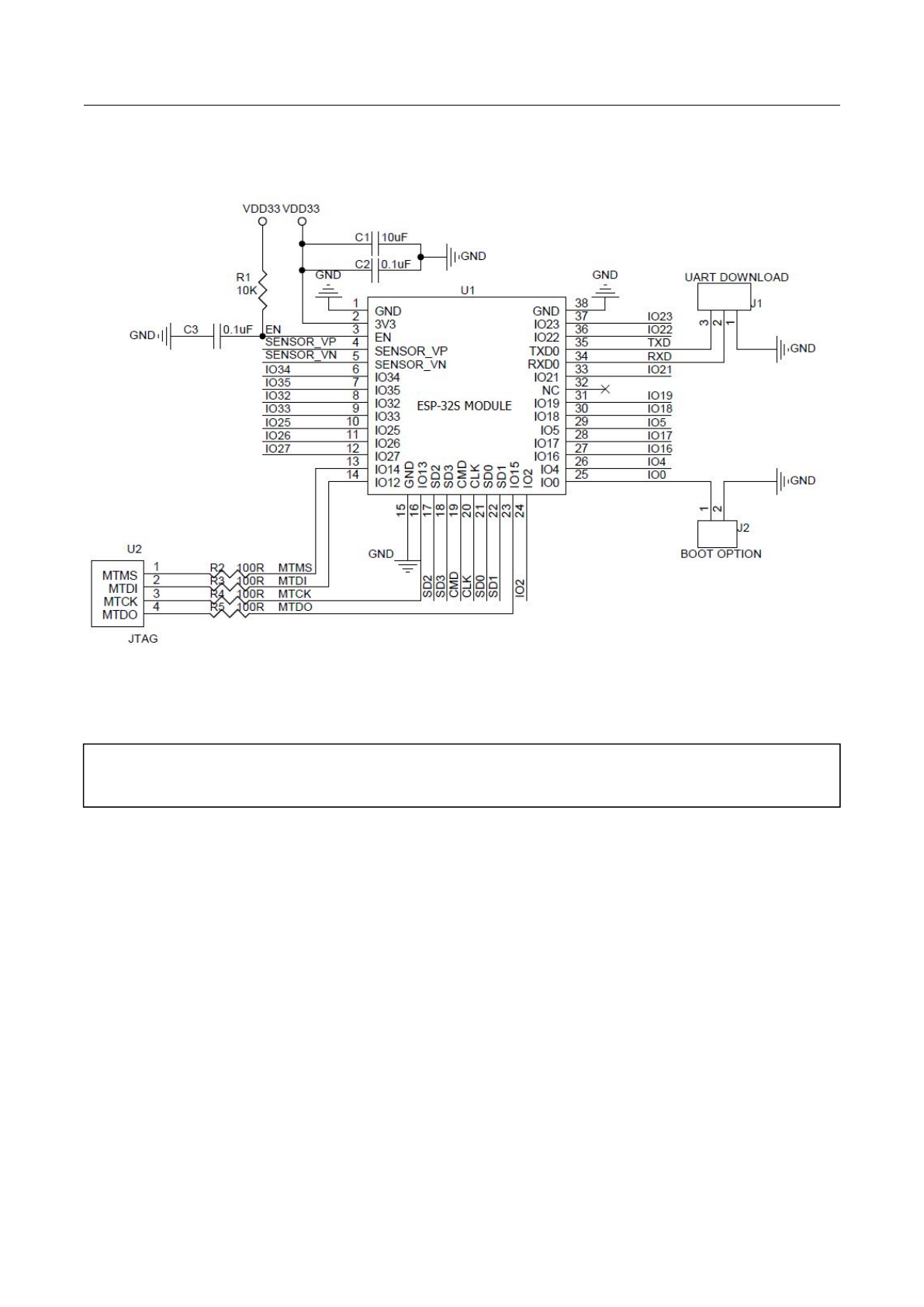
3.5.2 Peripheral Schematics
Figure 2: ESP-32S Peripheral Schematics
Note:
The MTDI should be kept at low electric level.

ESP-32S User Manual
Shenzhen Ai-Thinker Technology Co., Ltd http://www.ai-thinker.com
4. Electrical Characteristics
4.1 Absolute Maximum Ratings
Table 7: Absolute Maximum Ratings
Rating
Condition
Value
Unit
Storage temperature
-
-40 ~ 85
°C
Maximum soldering temperature
-
260
°C
Supply voltage
IPC/JEDEC J-STD-020
+2.2 〜+3.6
V
4.2 Recommended Operating Conditions
Table 8: Recommended Operating Conditions
Operating condition
Symbol
Min
Typ
Max
Unit
Operating temperature
-
-40
20
85
°C
Supply voltage
VDD
2.2
3.3
3.6
V
Operating current
IVDD
0.5
-
-
A
4.3 Digital Terminal Characteristics
Table 9: Digital Terminal Characteristics
Terminals
Symbol
Min
Typ
Max
Unit
Input logic level low
VIL
-0.3
-
0.25VDD
V
Input logic level high
VIH
0.75VDD
-
VDD+0.3
V
Output logic level low
VOL
N
-
0.1VDD
V
Output logic level high
VOH
0.8VDD
-
N
V
Note:
The specifications in this chapter have been tested under the following generalcondition: Vbat =3.3V’Ta
=27°C,unless otherwise specified.

ESP-32S User Manual
Shenzhen Ai-Thinker Technology Co., Ltd http://www.ai-thinker.com
4.4 Wi-Fi Radio
Table 10: Wi-Fi Radio Characteristics
Description
Min
Typ
Max
Unit
General Characteristics
Input frequency
2412
-
2484
MHz
Input impedance
-
50
-
Q
Input reflection
-
-
-10
dB
Output power of PA
15.5
19.5
21.5
dBm
Sensitivity
DSSS, 1 Mbps
-
-98
-
dBm
CCK, 11 Mbps
-
-90
-
dBm
OFDM, 6 Mbps
-
-93
-
dBm
OFDM, 54 Mbps
-
-75
-
dBm
HT20, MCS0
-
-93
-
dBm
HT20, MCS7
-
-73
-
dBm
HT40, MCS0
-
-90
-
dBm
HT40, MCS7
-
-70
-
dBm
MCS32
-
-91
-
dBm
Adjacent Channel Rejection
OFDM, 6 Mbps
-
37
-
dB
OFDM, 54 Mbps
-
21
-
dB
HT20, MCS0
-
37
-
dB
HT20, MCS7
-
20
-
dB
4.5 Bluetooth LE Radio
4.5.1 Receiver
Table 11: Receiver Characteristics - BLE
Parameter
Conditions
Min
Typ
Max
Unit
Sensitivity @0.1% BER
-
-
-98
-
dBm
Maximum received signal @0.1% BER
-
0
-
-
dBm
Co-channel C/I
-
-
+10
-
dB
F = F0+1 MHz
-
-5
-
dB
F = F0-1 MHz
-
-5
-
dB
Adjacent channel selectivity C/I
F = F0 + 2 MHz
-
-2 5
-
dB
F = F0-2 MHz
-
- 35
-
dB
F = F0 + 3 MHz
-
-25
-
dB
F = F0-3 MHz
-
-45
-
dB
30 MHz - 2000 MHz
-10
-
-
dBm
Out-of-band blocking performance
2000 MHz - 2400 MHz
-27
-
-
dBm
2500 MHz - 3000 MHz
-27
-
-
dBm
3000 MHz-12.5GHz
-10
-
-
dBm
Intermodulation
-
-36
-
-
dBm

ESP-32S User Manual
Shenzhen Ai-Thinker Technology Co., Ltd http://www.ai-thinker.com
4.5.2 Transmit
Table 12: Transmit Characteristics – BLE
Parameter
Conditions
Min
Typ
Max
Unit
RF transmit power
-
-
+7.5
+10
dBm
RF power control range
-
-
25
-
dB
Adjacent channel transmit power
F=F0+1 MHz
-
-14.6
-
dBm
F=F0-1 MHz
-
-12.7
-
dBm
F=F0 + 2 MHz
-
-44.3
-
dBm
F=F0-2 MHz
-
-38.7
-
dBm
F=F0 + 3 MHz
-
-49.2
-
dBm
F=F0-3 MHz
-
-44.7
-
dBm
F=F0+>3 MHz
-
-50
-
dBm
F=F0->3 MHz
-
-50
-
dBm
△f1avg
-
-
-
265
kHz
A f2
-
247
-
-
kHz
△f2avg/△f1avg
-
-
-0.92
-
-
ICFT
-
-
-10
-
kHz
Drift rate
-
-
0.7
-
kHz/50 µs
Drift
-
-
2
-
kHz
4.6 Reflow Profile
Table 13: Reflow Profile
Item
Value
Ts max to TL (Ramp-up Rate)
3°C/second max
Preheat
Temperature Min. (Ts Min.)
Temperature Typ. (Ts Typ.)
Temperature Min. (Ts Max.)
Time (Ts)
150°C
175°C
200°C
60 ~180 seconds
Ramp-up rate (TL to Tp)
3°C/second max
Time maintained above: -Temperature (TL)/Time (TL)
217°C/60 ~150 seconds
Peak temperature (Tp)
260°C max, for 10 seconds
Target peak temperature (Tp Target)
260°C +0/-5°C
Time within 5°C of actual peak (tp)
20~40 seconds
Ts max to TL(Ramp-down Rate)
6°C/second max
Tune25°C to Peak Temperature (t)
8 minutes max
ESP-32S User Manual
Shenzhen Ai-Thinker Technology Co., Ltd http://www.ai-thinker.com
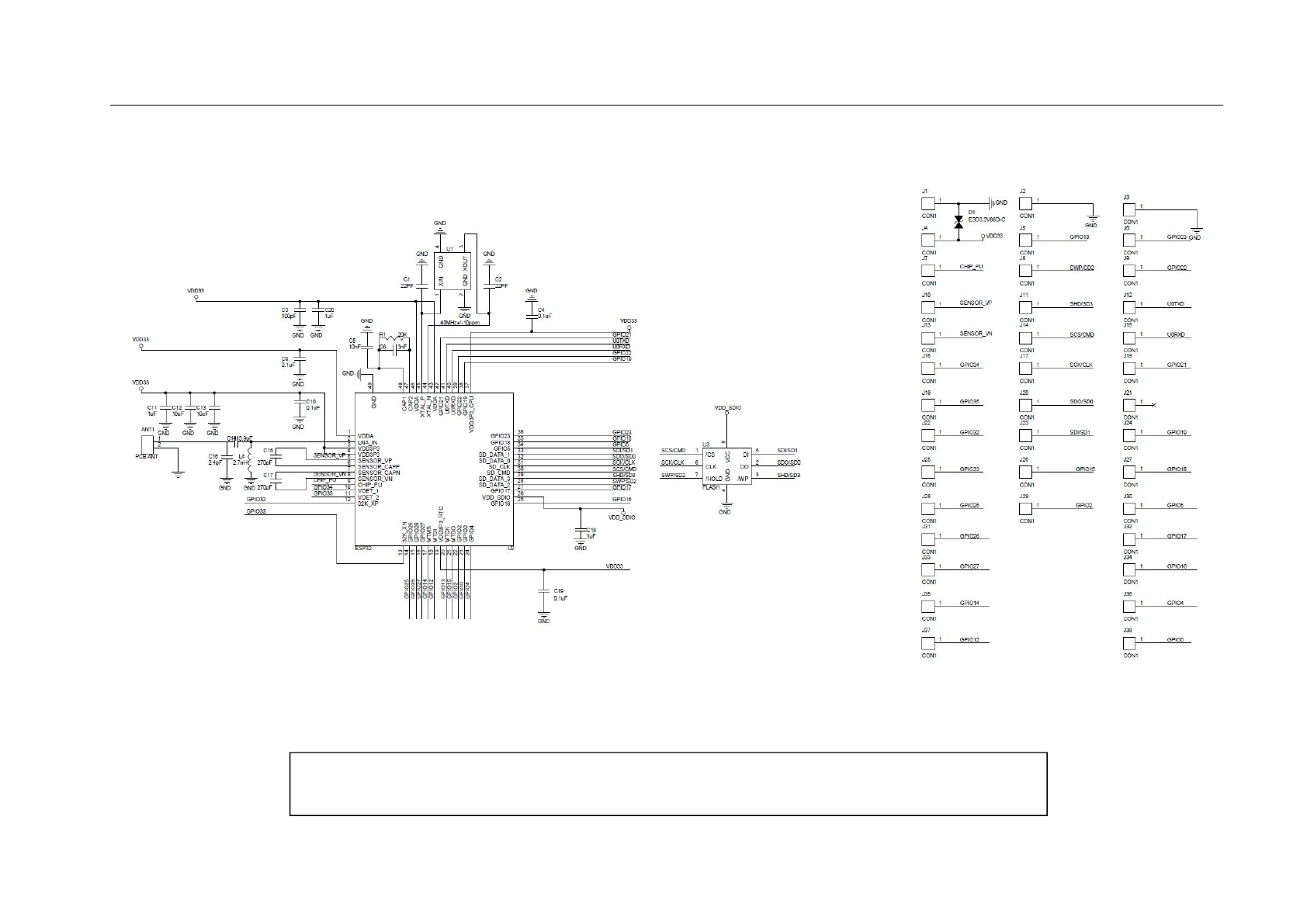
5. Schematics
Figure 3: ESP-32S Schematics
Note:
The capacitance of Gland C2 varies with the selection of the crystal.