Alereon AL5621 AL5621 PCB RADIO MODULE User Manual UG AL5621 EVB Rev2 0
Alereon, Inc AL5621 PCB RADIO MODULE UG AL5621 EVB Rev2 0
Alereon >
Users Guide
Rev. 2.0 – Mar 2008 Confidential Release Under Alereon NDA
USER GUIDE
INTRODUCTION
The AL5621 PCB Radio module is a complete compact device radio reference design that enables quick design of UWB enabled products.
The AL5621 combines the Alereon AL5000 chipset along with on board power supplies, an antenna output, and three different system
interfaces.
1.0 REFERENCE DESIGN FEATURES
QOptimized Performance with AL5100 (3.1GHz to 10.6GHz) All Worldwide Bands.
QComplete Baseband Processor (BBP) and Media Access Controller (MAC)
QHigh Precision Data Path and Data Converters allowing reliable link at extended ranges
QFully Integrated MAC Protocol Engine Supports All Industry Standards WiMedia Protocols
— Certified Wireless USB
— WiMedia Link Layer Protocol
— Bluetooth 3.0 (supported by future SW releases)
QIndustry Standard Interfaces
— ULPI 1.1 Interface: 8-Bit / 12 Pins for USB 2.0 PHYs
— CF+ 3.0 / Generic Parallel Interface: 8 & 16-Bits
— SDIO 1.1 Interface 1-Bit and 4-Bit Modes
— UART interface for Cable Associate function
QOperates from a single (+3.3 V, regulated) supply
QSmall Form Factor (38.46 x 27.18 mm) (1.5 x 1 in)
Q3 GPIO lines for LEDs or additional control signals
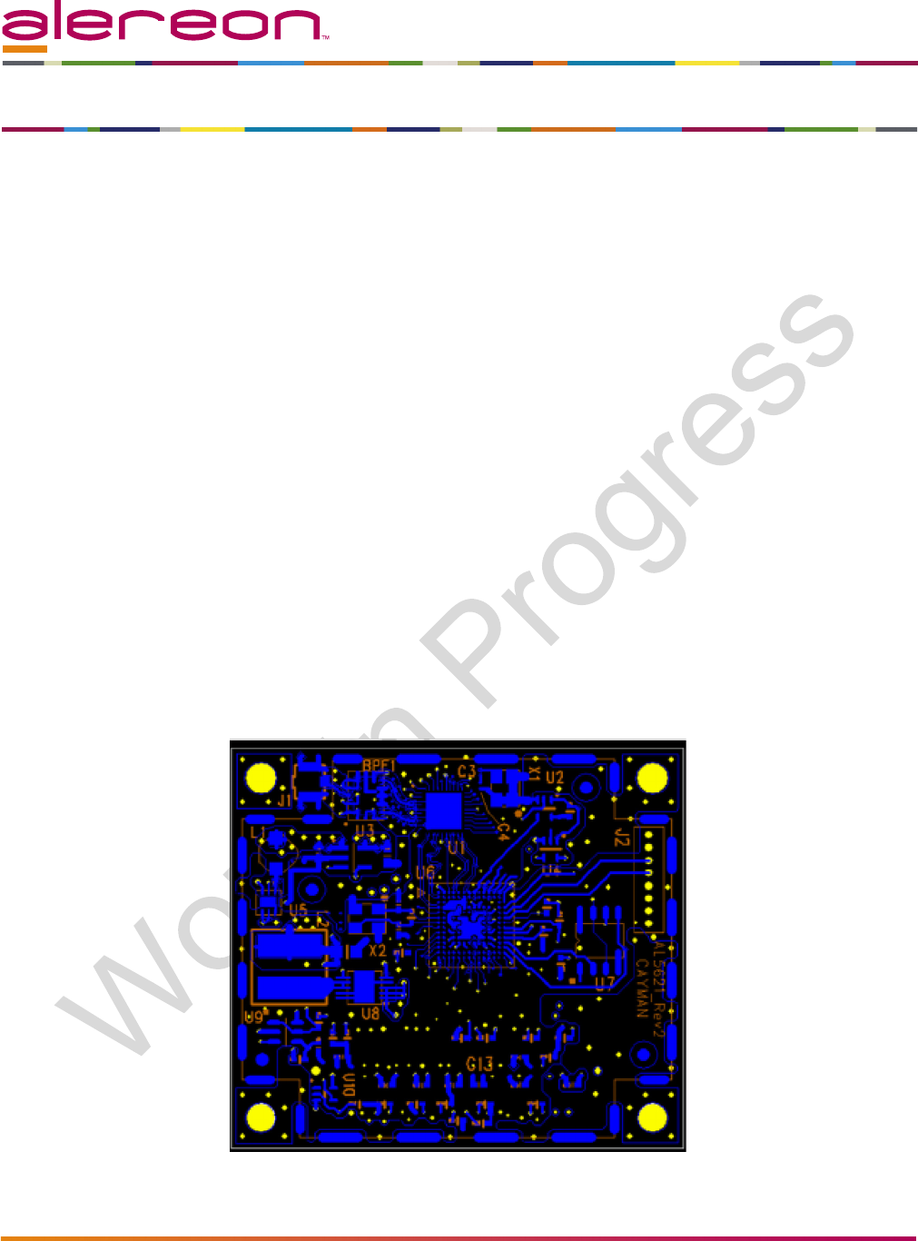
Figure 1. AL5621 Worldwide Radio Card
AL5621 Rev 2 Worldwide Wireless USB Device Radio Card Evaluation Board User Guide
AL5621 Rev 2 Worldwide Wireless USB Device Radio Card Evaluation Board User Guide User Guide
2Rev. 2.0
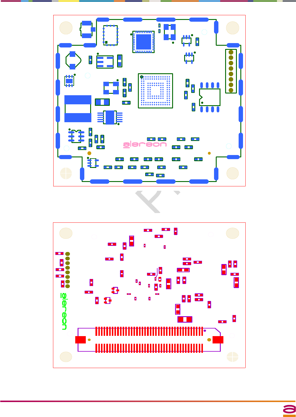
Figure 2. Design Overview - Top Side
Figure 3. Design Overview - Bottom Side
B
U4 J2
R6 R7
R16
C16
R24
R22
U6
R12
C14
C15
R23
C12
BPF1
U3
X2
R2
C7
C9
R11
R19R17
C11
J1
C1
R9
R1
U7
U2
R5 R4
R14
R15
X1
C3
C4
R13
C13
R3
R21
U1
R20
C2
U8
C6
R18
C10
R10
U10
C8
C5
L2
U9
R8
L1
U5
SHLD1
B
R29
R37
R28
C35 Q2
R25
C26
J3
R31
C20
R30
R40
C23
C36
R27
C21
R45
C41
R26
R32
C29
C30
C39
C42
R33
R47
R34
R48
R35
R36
R38
R39
Q1
C18
C17
C37
C19 C24
C25
C28
C27
C38
R42 L3
R41
C22
C31
C40
R43
R44
C43
R46
C32
C44
C33
R49
C34
User Guide AL5621 Rev 2 Worldwide Wireless USB Device Radio Card Evaluation Board User Guide
Rev. 2.0 3
2.0 BLOCK DIAGRAM
Figure 4. AL5621 Block Diagram
3.0 USER I/O INTERFACE HEADERS ULPI / SDIO / CF+ (BASE MOTHERBOARD CONNECTIONS)
AL5300
BBP/MAC
AL5100 RF
Transceiver
BDF
U.FL
Application
Interface
Host Interface
Connectors
(+3.3 V)
(Control)
(ULPI)
(SDIO)
(CF+)
(GPIO)
(Reset)
Control
Signals
Flash
Memory
+1.2 V
+3.3 V
+2.4 V
Power up
Reset
Reset
GPIO
20 MHz 44 MHz
AL5621 Rev 2 Worldwide Wireless USB Device Radio Card Evaluation Board User Guide User Guide
4Rev. 2.0
4.0 DESIGN CONSIDERATIONS
4.1 Power
One +3.3 V power supply at max data rate average current of 500 mA with peak at 750 mA.
4.2 Board Reset
During power up, an "on board" power monitor holds the board Reset for approximately 150 ms. The card can also be reset at any time by asserting the
"Card_Reset#" signal low.
It is also important to note that the Mode Pins HSTIF_SEL_0 & HSTIF_SEL_1 are sampled on the rising edge of Card_Reset#.
4.3 Mode Switching
During Power-Up, the HSTIF_SEL pins are sampled to configure the AL5300 HSTIF pins to one of three different host interface operating modes. The
HSTIF_SEL pins must remain static for the duration of the operation of the AL5300 BBP/MAC.
Table 1 shows the proper settings of the HSTIF_SEL pins.
4.4 Firmware Boot-Up
After completing the power-up cycle and after Card_Reset# is de-asserted, the AL5300 BBP/MAC automatically loads the Executable and Linking Format
(ELF) firmware image into the chip’s internal instruction memory. There are two boot modes, SPI and HOST. When utilizing SPI boot mode, the ELF image
is loaded from an external EEPROM, which is connected to the AL5300 BBP/MAC using an industry standard 4-wire SPI port. When utilizing HOST boot
mode, the ELF image is loaded directly over the HSTIF through either CF+, SDIO, or ULPI, and eliminates the need for an external EEPROM. Once the ELF
image has been loaded, the AL5300 BBP/MAC will provide a software handshake to the Alereon software drivers indicating that the AL5300 BBP/MAC is
ready for normal operation. The state of the HOST_BOOT pin determines which of two modes is used (refer to Table 2).
5.0 CF+ SIGNAL DEFINITIONS
The CF+/General Purpose Parallel interface can be configured as either a 8-bit or 16-bit parallel data port. The AL5300 BBP/MAC utilities a FIFO memory
buffer at the interface, allowing for simple and efficient high throughput data transfers without affecting the operation of the wireless link. The CF+/General
Purpose Parallel interface can be configured and used in accordance to the CF+ specification (CompactFlash, Revision 3.0). When used as a CF+ port, the
interface is compatible to both the I/O and Memory modes of operation.
The features of the AL5300 BBP/MAC CF+/General Purpose Parallel interface include:
• Interrupt-driven interface (the AL5300 BBP/MAC will interrupt the host system)
• 10 registers used to distinguish data and control spaces
• Payload data is ordered by a FIFO and is pushed or pulled through a single address
• Data and control registers can be accessed either as a 8-bit or 16-bit data word
Table 3 provides a listing of the CF+ interface pins and their functions.
Table 1. HSTIF_SEL Pin Settings
Host Interface Mode HSTIF_SEL[1:0]*
CF+/ Generic Parallel 00
SDIO 01
ULPI 10
Reserved 11
*Note: Please connect the HSTIF_SEL pins to GND for a “0” or do not connect
them for a “1”. Both HSTIF_SEL signals are pulled high on the daughter
board through a 10K resistor to VDD. 0 = GND; 1 = No-Connect.
Table 2. Boot Modes
Boot Mode HOST_BOOT*
SPI Boot Mode 0
Host Boot Mode 1
*Note: Please connect HOST_BOOT through a 330 Ω resistor to GND for “0” or No-
Connect for “1”. 0 = 330 Ω to GND; 1 = No-Connect.

User Guide AL5621 Rev 2 Worldwide Wireless USB Device Radio Card Evaluation Board User Guide
Rev. 2.0 5
Table 3. CF+/General Purpose Parallel Interface Pin Descriptions
AL5300 Pin Name Type Description
P8, P7, P6, P5, L5, P4,
N4, N3, P1, N1, L2 ADDR[10:0] Input
Memory Mode: These address lines along with the CF_REG# signal are used to select the following: The I/O port
address registers within the generic parallel interface/CF+ Card, the memory mapped port address registers within
the generic parallel interface/CF+ Card, a byte in the card's information structure and its configuration control and
status registers.
IO Mode: This signal is the same as the Memory Mode signal.
L10, N11, N12, N13, P14,
J1, J2, K1, P10, P11,
P12, P13, N14, J4, K2, L1
DATA[15:0]
Bi-
Direction
al
Memory Mode: These lines carry the Data, Commands and Status information between the host and the controller.
DATA0 is the Least Significant Bit (LSB) of the Even Byte of the Word. DATA8 is the LSB of the Odd Byte of the Word.
Note: When operating in 8 bit mode, DATA[15:8] are ignored.
IO Mode: This signal is the same as the Memory Mode signal.
P3 CF_RESET Input
Memory Mode*: The generic parallel interface/CF+ Card is Reset when the RESET pin is high with the following
important exception: The host may leave the RESET pin open or keep it continually high from the application of
power without causing a continuous Reset of the card. Under either of these conditions, the card shall emerge from
power-up having completed an initial Reset.
The generic parallel interface/CF+ Card is also Reset when the Soft Reset bit in the Card Configuration Option
Register is set.
IO Mode*: This signal is the same as the Memory Mode signal.
*Note: CF_RESET is used to reset the CF+/General Purpose Parallel ports controller independently of the
AL5300 BBP/MAC. Asserting CF_RESET will NOT reset the AL5300 BBP/MAC.
P9 CF_CE1# Input
Memory Mode: These input signals are used both to select the card and to indicate to the card whether a byte or a
word operation is being performed. CF_CE2# always accesses the odd byte of the word. CF_CE1# accesses the
even byte or the Odd byte of the word depending on ADDR0 and CF_CE2#.
IO Mode: This signal is the same as the Memory Mode signal.
N9 CF_CE2# Input
Memory Mode: These input signals are used both to select the card and to indicate to the card whether a byte or a
word operation is being performed. CF_CE2# always accesses the odd byte of the word. CF_CE1# accesses the
even byte or the Odd byte of the word depending on ADDR0 and CF_CE2#.
IO Mode: This signal is the same as the Memory Mode signal.
N8 CF_OE# Input
Memory Mode: This is an Output Enable strobe generated by the host interface. It is used to read data from the
generic parallel interface/CF+ Card in Memory Mode and to read the CIS and configuration registers.
IO Mode: In I/O Mode, this signal is used to read the CIS and configuration registers.
L6 CF_WE# Input
Memory Mode: This is a signal driven by the host and used for strobing memory write data to the registers of the
generic parallel interface/CF+ Card when the card is configured in the memory interface mode. It is also used for
writing the configuration registers.
IO Mode: In I/O Mode, this signal is used for writing the configuration registers.
N5 CF_IREQ# Output
Memory Mode: In Memory Mode, this signal is set high when the generic parallel interface/CF+ Card is ready to
accept a new data transfer operation and is held low when the card is busy. At power up and at Reset, the CF_IREQ#
signal is held low (busy) until the generic parallel interface/CF+ Card has completed its power up or reset function.
No access of any type should be made to the generic parallel interface/CF+ Card during this time.
Note, however, that when a card is powered up and used with CF_IREQ# continuously disconnected or asserted,
the Reset function of the CF_IREQ# pin is disabled. Consequently, the continuous assertion of CF_IREQ# from the
application of power shall not cause the READY signal to remain continuously in the busy state.
IO Mode: After the generic parallel interface/CF+ Card has been configured for I/O operation, this signal is used as
Interrupt Request#. This line is strobed low to generate a pulse mode interrupt or held low for a level mode interrupt.
L8 CF_IORD# Input
Memory Mode: This signal is not used in this mode.
IO Mode: This is an I/O Read strobe generated by the host. This signal gates I/O data onto the bus from the generic
parallel interface/CF+ Card when the card is configured to use the I/O interface.
N7 CF_IOWR# Input
Memory Mode: This signal is not used in this mode.
IO Mode: The I/O Write strobe pulse is used to clock I/O data on the bus into the generic parallel interface/CF+ Card
controller registers when thickeners parallel interface/CF+ Card is configured to use the I/O interface. The clocking
shall occur on the negative to positive edge of the signal (trailing edge).
K4 CF_STSCHG# Output
Memory Mode: This signal is asserted high, as BVD1 is not supported.
IO Mode: This signal is asserted low to alert the host to changes in the READY and Write Protect states, while the
I/O interface is configured. Its use is controlled by the Card Config and Status Register.
M1 CF_REG# Input
Memory Mode: This signal is used during Memory Cycles to distinguish between Common Memory and Register
(Attribute) Memory accesses. High for Common Memory, Low for Attribute Memory.
IO Mode: The signal shall also be active (low) during I/O Cycles when the I/O address is on the Bus.
N2 CF_INPACK# Output
Memory Mode: This signal is not used in this mode.
IO Mode: The Input Acknowledge signal is asserted by the generic parallel interface/CF+ Card when the card is
selected and responding to an I/O read cycle at the address that is on the address bus. This signal is used by the
host to control the enable of any input data buffers between the generic parallel interface/CF+ Card and the CPU.
H1 CF_IOIS16# Output
Memory Mode: The generic parallel interface/CF+ Card does not have a write protect switch. This signal is held low
after the completion of the reset initialization sequence.
IO Mode: When the generic parallel interface/CF+ Card is configured for I/O Operation, this pin is used for the
CF_IOIS16# function. A Low signal indicates that a 16-bit or odd byte only operation can be performed at the
addressed port.
P2 CF_WAIT# Output
Memory Mode: The CF_WAIT# signal is driven low by the generic parallel interface/CF+ Card to signal the host to
delay completion of a memory or I/O cycle that is in progress.
IO Mode: This signal is the same as Memory Mode signal.
AL5621 Rev 2 Worldwide Wireless USB Device Radio Card Evaluation Board User Guide User Guide
6Rev. 2.0
6.0 SDIO SIGNAL DEFINITIONS
The SDIO interface supports both 1-bit and 4-bit Modes of operation and is fully compliant with SDIO Card Specification, Version 1.1. The SDIO interface
can be double clocked, up to 50 MHz, providing twice the throughput of standard SDIO. Similar to the CF+/General Purpose Parallel interface, the SDIO
interface utilizes a FIFO memory buffer at the interface to buffer the transactions on the host interface from those on the wireless link. Tabl e 4 provides a
listing of the SDIO interface pins and their functions.
Note: The host must pull-up SDIO_D0, SDIO_D1, SDIO_D2, and SDIO_D3 even if the host uses SD Memory Card as 1 bit mode-only in SD mode.
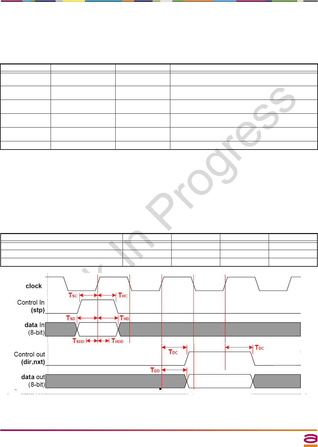
7.0 ULPI SIGNAL DEFINITIONS
The AL5300 BBP/MAC host interface complies with the ULPI Specification, Revision 1.1, which is compatible with USB 2.0. The ULPI specification provides
a low-pin, low-cost, small form-factor transceiver interface for any USB application. Control and data timing requirements are given in Table 5 and illustrated
in Figure 5. These timings apply to Synchronous Mode only. All timings are measured with respect to the clock as seen at the ULPI input clock pin
(ULPI_CLKI). Control signals and 8-bit data are always clocked on the rising edge of the clock, while the optional double-edge 4-bit data signals are clocked
on rising and falling edges. This interface runs at a clock speed of 60 MHz.
Figure 5. ULPI Timing Diagram
Table 4. SDIO Host Interface Pin Descriptions
Pin Name Type Description
L1 SDIO_DATA0 BiDirectional SD 4-bit mode: Data Line 0
SD1-bit mode: Data Line
K2 SDIO_D1 BiDirectional SD4 bit mode: Data Line 1 or Interrupt (optional)
SD1 bit mode: Interrupt
J4 SDIO_D2 BiDirectional SD4 bit mode: Data Line 2 or Read Wait (optional)
SD1 bit mode: Read Wait (optional)
N14 SDIO_D3 BiDirectional SD4 bit mode: Data Line 3
SD1 bit mode: Not Used
P13 SDIO_CMD BiDirectional SD4 bit mode: Command Line
SD1 bit mode: Command Line
N7 SDIO_CLK Input SD Clock
Table 5. ULPI Interface Timing
Parameter Symbol Min Max Units
Setup time (control in, 8-bit data in) TSC, TSD 6.0 ns
Hold time (control in, 8-bit data in) THC, THD 0.0 ns
Output delay (control out, 8-bit data out) TDC, TDD 9.0 ns
User Guide AL5621 Rev 2 Worldwide Wireless USB Device Radio Card Evaluation Board User Guide
Rev. 2.0 7
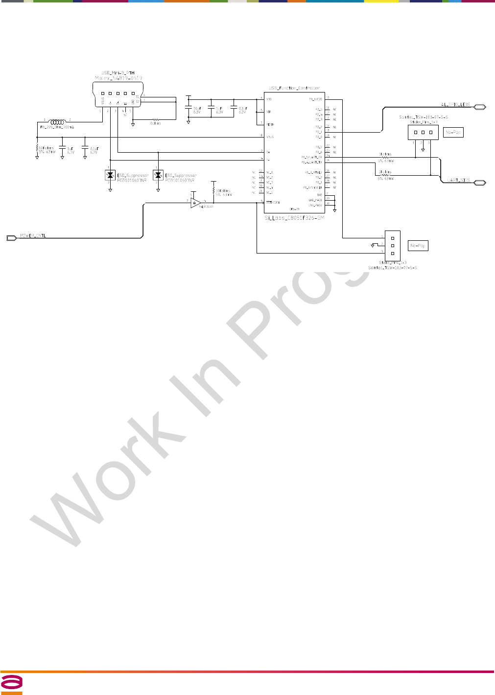
8.0 CABLE ASSOCIATION SUPPORT
If the end product requires Cable Association support per the Wireless USB security specification, the following circuit must be added to the base motherboard
design.
Figure 6. Cable Association Schematic Example
USB_FC_DU-
USB_FC_DU+
USB_UPCONN_SHLD
AL_GPIO_LEDS
POWER_CNTL
USB_FC_RST#/C2CK
USB_FC_RST#/C2CK
USB_FC_C2D
USB_FC_TX
USB_FC_RX
UART_SIGS
VBUS_UP_FLTR
VBUS_UP_CONN
D23 D22
R78
J13
AL_GPIO_2
PWR_ON_RESET#
C217
+3.3V
C70
J14
U17
+3.3V R80
+3.3V
J15
UART_RXD
UART_TXD
C71
R79
L10
R76
R77
C216
C69
U16
AL5621 Rev 2 Worldwide Wireless USB Device Radio Card Evaluation Board User Guide User Guide
8Rev. 2.0
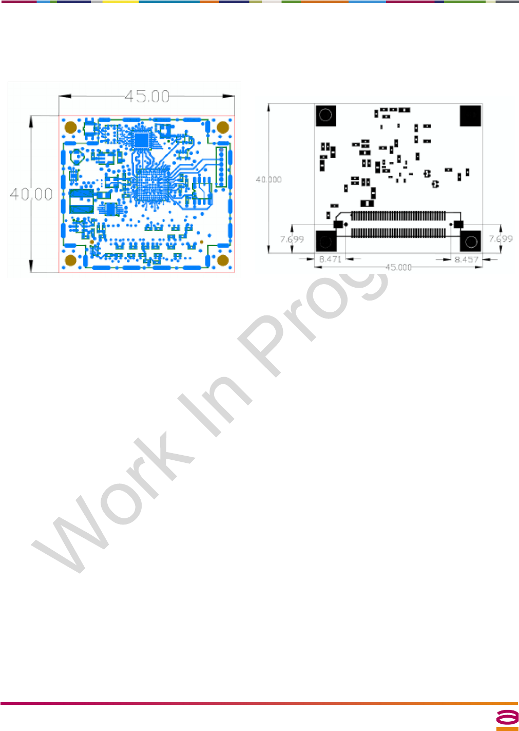
9.0 MECHANICAL MOTHERBOARD DESIGN CONSIDERATIONS
The AL5621 schematics and "AL5621 to Motherboard" connector data sheets can be found in the AL5621-RDK (Reference Design Kit). The following
drawing shows the mechanical requirements for the placement of the two AL5621 interface connectors that are required for Electro-Mechanical connection
between the product's base motherboard and the AL5621 Radio module.
Figure 7. AL5621 Module Mechanical Diagram
10.0 PRODUCT DESIGN UPDATES
Design enhancements for all Alereon design are continually made. Please visit the Alereon NDA web site periodically to ensure you stay up to date with the
lasted design changes, as well as schematic and Reference Design Kit revisions.

User Guide AL5621 Rev 2 Worldwide Wireless USB Device Radio Card Evaluation Board User Guide
Rev. 2.0 9
REVISION HISTORY
Date Version Description
01/03/2008 1.0 Initial Release Version
03/03/2008 2.0 Document updated to reflect Rev 2 board revision.

Alereon, Inc.
7600 North Capital of Texas Highway
Building C, Suite 200
Austin, TX 78731
Telephone: (512) 345-4200
Fax: (512) 345-4201
info@alereon.com
The contents of this document are provided in connection with Alereon, Inc. products. Alereon makes no representations or warranties with respect to the accuracy or completeness of the contents of
this publication and reserves the right to make changes to specifications and product descriptions at any time without notice. No license, whether express, implied, arising by estoppel or otherwise, to
any intellectual property rights is granted by this publication. Except as set forth in Alereon's Standard Terms and Conditions of Sale, Alereon assumes no liability whatsoever, and disclaims any express
or implied warranty, relating to its products including, but not limited to, the implied warranty of merchantability, fitness for a particular purpose, or infringement of any intellectual property right.
Alereon's products are not designed, intended, authorized or warranted for use as components in systems intended for surgical implant into the body, or in other applications intended to support or sustain
life, or in any other application in which the failure of Alereon's product could create a situation where personal injury, death, or severe property or environmental damage may occur. Alereon reserves
the right to discontinue or make changes to its products at any time without notice.
© 2008 Alereon, Inc.
All rights reserved.
Trademarks
Alereon, the Alereon logo and combinations thereof are trademarks of Alereon, Inc.
Other product names used in this publication are for identification purposes only and may be trademarks of their respective companies.