Amazon com Services 2105 Data Module User Manual Installation Manual
Folksy LLC Data Module Installation Manual
UserManual.wiki
>
Amazon com Services
>
2105 User Manual
Installation Manual
Navigation menu
Upload a User Manual
Namespaces
Wiki Guide
HTML
PDF
Info
Views
User Manual
Discussion / Help
Navigation
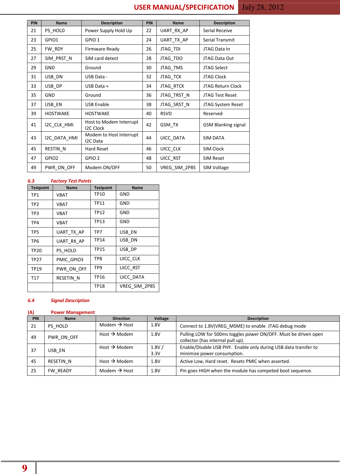
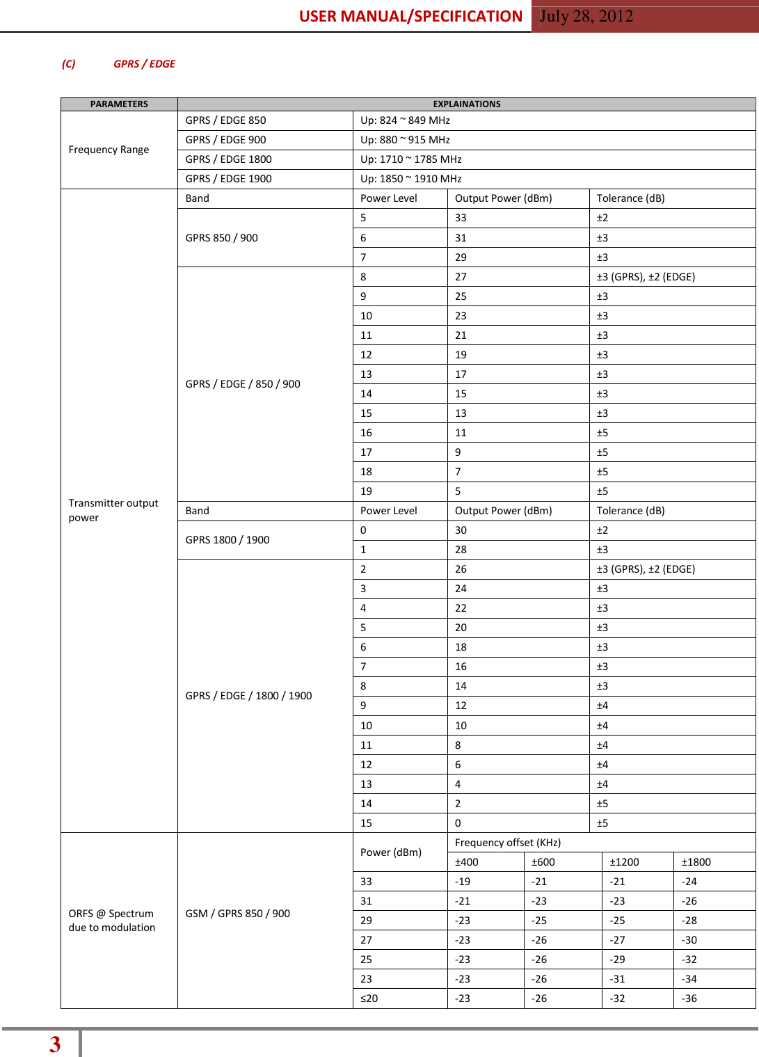
![USER MANUAL/SPECIFICATION July 28, 2012 1 REVISION HISTORY REV ECO CHANGE DESCRIPTION APPROVED BY DATE 1.0 Initial release 07/28/12 1. GENERAL SPECIFICATIONS OF MODULE. PARAMETERS EXPLAINATIONS Air Interfaces WCDMA Band I, II, V, VIII GPRS / EDGE 850, 900, 1800, 1900 LTE Band IV, XVII Protocols LTE: Rel 8, Cat 3 WCDMA / HSDPA / HSUPA: Rel 7 GSM / GPRS / EDGE : Rel 6 Max Data Rate LTE 100 Mbps Down (64QAM) / 50 Mbps Up (16QAM) HSDPA Cat 14 21.1 Mbps Down HSUPA Cat 6 5.76 Mbps Up WCDMA 384 Kbps Down / Up GPRS Multi slot class 10, CS-4 80 Kbps Down / 20 Kbps Up EDGE MCS-9, 236.8 Kbps Down / 59.2 Kbps Up RX / TX Frequency Interval LTE Band IV 400 MHz LTE Band XVII 30 MHz WCDMA / HSPA 850 45 MHz WCDMA / HSPA 1900 80 MHz WCDMA / HSPA 2100 190 MHz WCDMA / HSPA 900 45 MHz GPRS / EDGE 850 45 MHz GPRS / EDGE 900 45 MHz GPRS / EDGE 1800 95 MHz GPRS / EDGE 1900 80 MHz Max Output Power (single slot) LTE Band IV 24 dBm (Power class 3) LTE Band XVII 23 dBm (Power class 3) WCDMA / HSPA 23 dBm (Power class: 3) GPRS 850 / 900 32 dBm (Power class: 4) GPRS 1800 / 1900 29.5 dBm (Power class: 1) EDGE 850 / 900 26.5 dBm (Power class: E2) EDGE 1800 / 1900 25.5 dBm (Power class: E2) Operating Voltage VBATT 3.4V ~ 4.2V Sleep / Off Current Off Leakage 5uA Rock Bottom [Sleep] 2mA Standby Current (single cell, no neighbors) LTE standby 128 Frames 5.15mA WCDMA standby 64 Frames 128 Frames 256 Frames 512 Frames 5.51mA 4.15mA 3.05mA 2.90mA GPRS standby MFRMS = 2 5.8mA Peak Current 2.0A max, 600µs, 12.5 % Duty Cycle Operating Temperature Range -10°C ~ +55°C Storage Temperature Range -30°C ~ +80°C](https://usermanual.wiki/Amazon-com-Services/2105/User-Guide-1784812-Page-2.png)
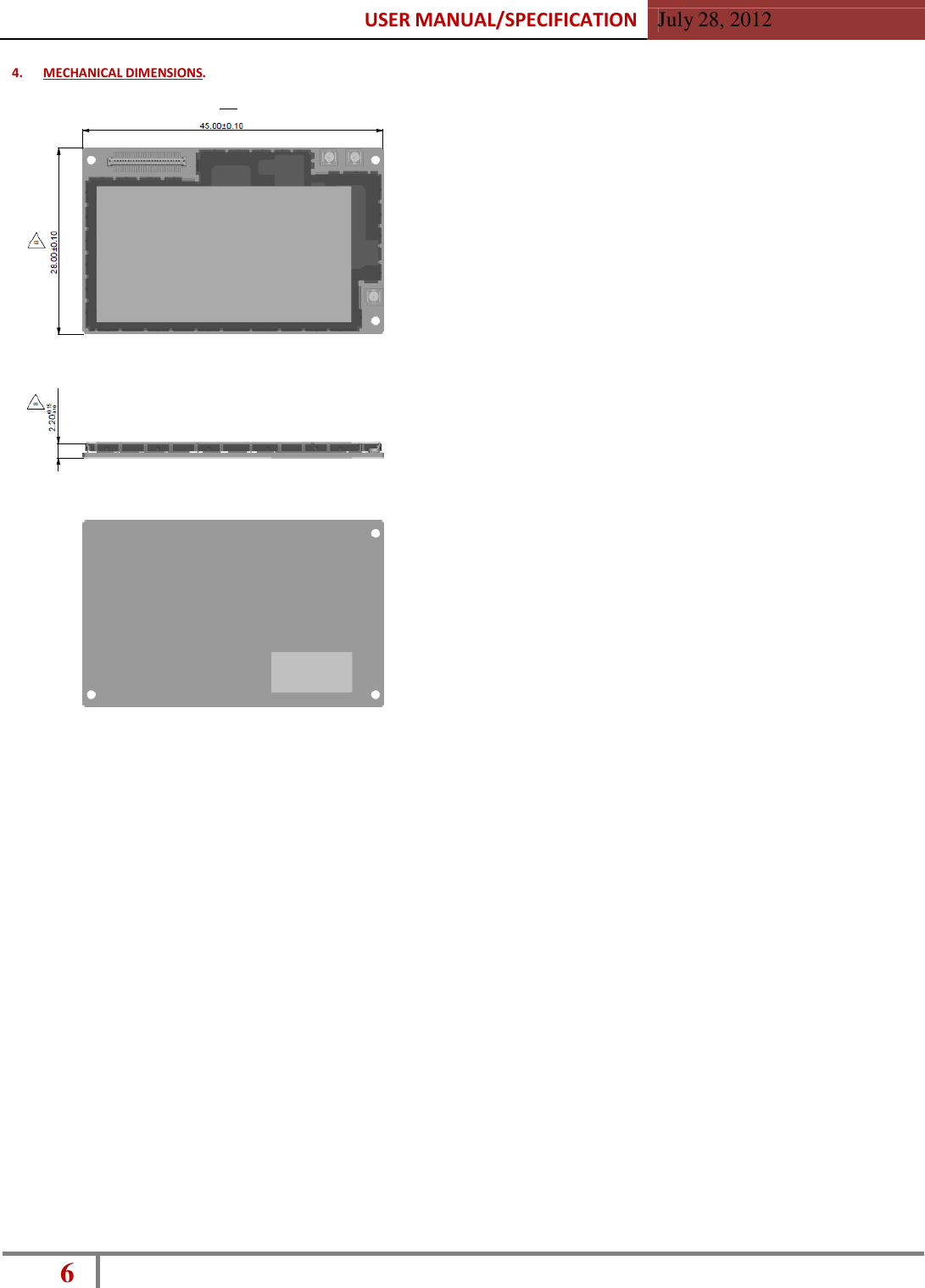
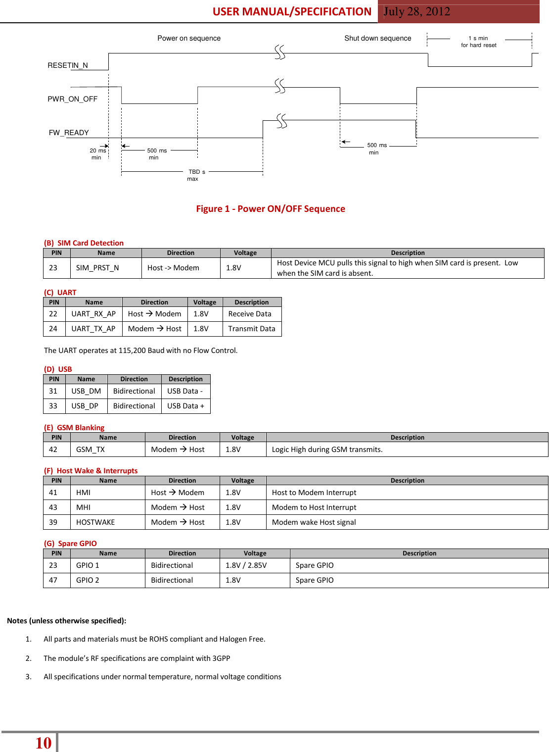
![USER MANUAL/SPECIFICATION July 28, 2012 2 PARAMETERS EXPLAINATIONS Frequency Stability WCDMA / HSDPA 800 ±0.1ppm WCDMA / HSDPA 900 ±0.1ppm WCDMA / HSDPA 1800 ±0.1ppm WCDMA / HSDPA 1900 ±0.1ppm WCDMA / HSDPA 2100 ±0.1ppm LTE Band IV ±0.1ppm LTE Band XVII ±0.1ppm GSM / GPRS ±0.1ppm Physical Dimensions 1 48.00 x 28.00 x 2.1 mm Weight 6.9g 2. TRANSMIT SPECIFICATIONS. (A) LTE PARAMETERS EXPLAINATIONS Frequency Range Band IV [AWS] Up: 1710 ~ 1755 MHz Band XVII [700] Up: 704 ~ 716 MHz Max Output Power 23dBm ±2 dBm Min Output Power Below -40dBm Error Vector Magnitude 17.5% QPSK or BPSK 12.5% 16QAM ACLR1 30dB 1.4, 3, 5, 10, 15, 20 MHz bandwidth ACLR2 33dB 1.4, 3, 5, 10, 15, 20 MHz bandwidth (B) WCDMA/HSDPA PARAMETERS EXPLAINATIONS Frequency Range 2100 (Band I) Up: 1920 ~ 1980 MHz 1900 (Band II) Up: 1850 ~ 1910 MHz 850 (Band V) Up: 824 ~ 849 MHz 900 (Band VIII) Up: 880 ~ 915 MHz Max Output Power 24dBm +1/-3 dBm Min Output Power Below -50dBm Spectrum Emission Mask Below -35 dBc 2.5 – 3.5 MHz Offset 30KHz Below -35 dBc 3.5 – 7.5 MHz Offset 1MHz Below -39 dBc 7.5 – 8.5 MHz Offset 1MHz Below -49 dBc 8.5 – 12.5 MHz Offset 1MHz Occupied Bandwidth Below 5MHz ACLR ±5MHz 33dB, ±10MHz 43dB](https://usermanual.wiki/Amazon-com-Services/2105/User-Guide-1784812-Page-3.png)
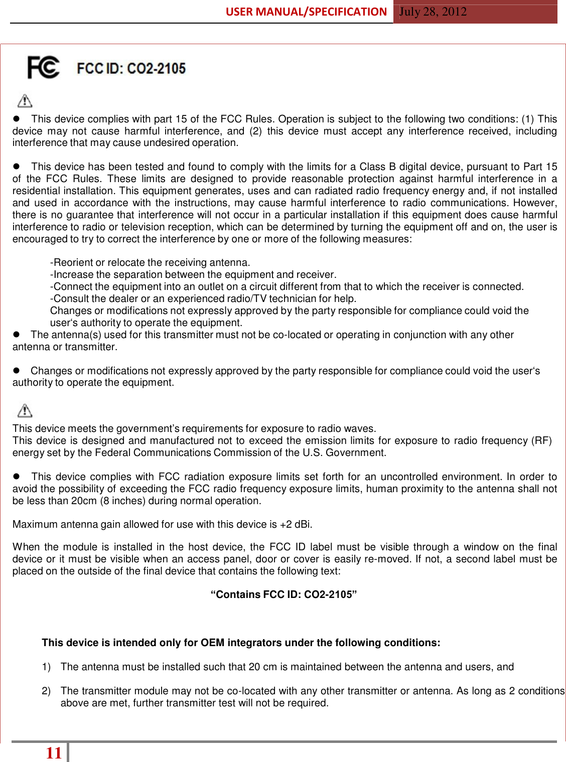
![USER MANUAL/SPECIFICATION July 28, 2012 4 PARAMETERS EXPLAINATIONS ORFS @ Spectrum due to switching transient GSM / GPRS 1800 / 1900 Power (dBm) Frequency offset (KHz) ±400 ±600 ±1200 ±1800 30 -22 -24 -24 -27 28 -23 -25 -26 -29 26 -23 -26 -28 -31 24 -23 -26 -30 -33 22 -23 -26 -31 -35 ≤20 -23 -26 -32 -36 3. RECEIVE SPECIFICATIONS. (A) LTE PARAMETERS EXPLAINATIONS Frequency Range Band IV [AWS] Down: 2110 ~ 2155 MHz Band XVII [700] Down: 734 ~ 746 MHz Reference Sensitivity Level Band IV BW (MHz) Reference Sensitivity (dBm) Modulation 5 -100 QPSK 10 -97 QPSK Band XVII BW (MHz) Reference Level (dBm) Modulation 5 -97 QPSK 10 -94 QPSK Adjacent Channel Selectivity BW (MHz) Adjacent Channel Selectivity (dB) 5 33 dB 10 33 dB (B) WCDMA/HSDPA PARAMETERS EXPLAINATIONS Frequency Range Band I [2100] Down: 2110 ~ 2170 MHz Band II [1900] Down: 1930 ~ 1990 MHz Band V [850] Down: 869 ~ 894 MHz Band VIII [900] Down: 925 ~ 960 MHz Reference Sensitivity Level WCDMA Band I -106.7 dBm WCDMA Band II -104.7 dBm WCDMA Band V -104.7 dBm WCDMA Band VIII -103.7 dBm Adjacent Channel Selectivity Band I -92.7 dBm -52dBm @ ±5MHz Band II -90.7 dBm Band V -90.7 dBm Band VIII -89.7 dBm Intermodulation Band I -103.7 dBm -46dBm ±10MHz, ±20MHz Band II -101.7 dBm Band V -101.7 dBm Band VIII -100.7 dBm Spurious Response Band I -103.7 dBm -44 dBm Band II -101.7 dBm Band V -101.7 dBm Band VIII -100.7 dBm In-Band Blocking Band I -103.7 dBm -56 dBm @ ±10MHz, -44 dBm @ ±15MHz Band II -101.7 dBm](https://usermanual.wiki/Amazon-com-Services/2105/User-Guide-1784812-Page-5.png)