Amimon AMN11100R44 AMN11100 Transmitter - WHDI Wireless Modules User Manual AMN11100 WHDI Transmitter Module Datasheet
Amimon Ltd. AMN11100 Transmitter - WHDI Wireless Modules AMN11100 WHDI Transmitter Module Datasheet
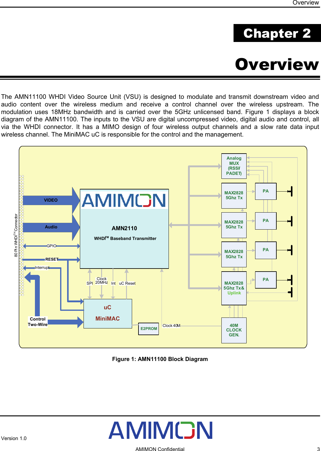
Amimon >
User Manual
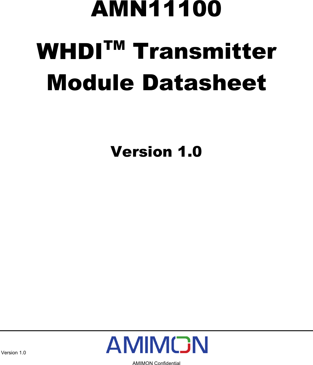

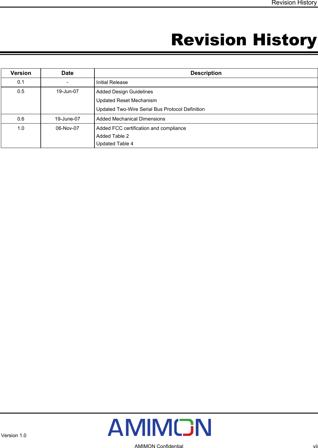
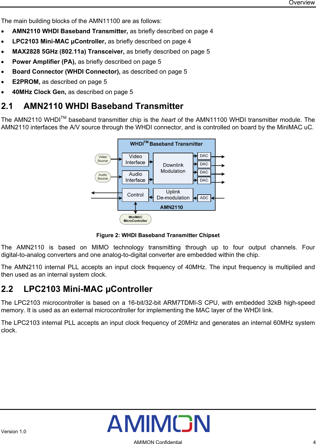
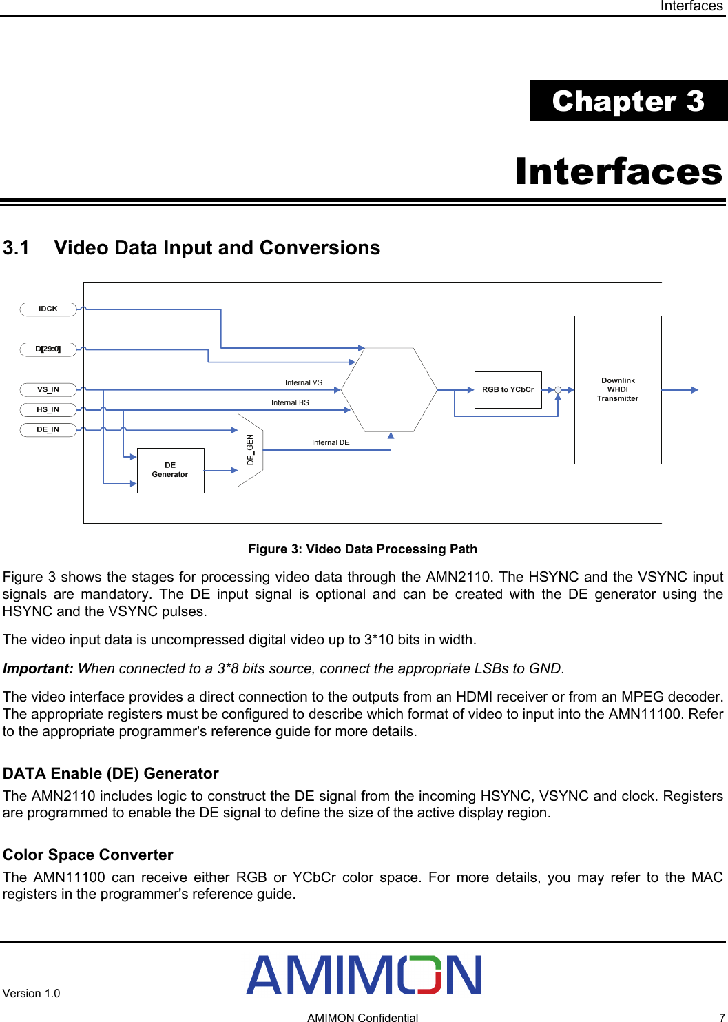
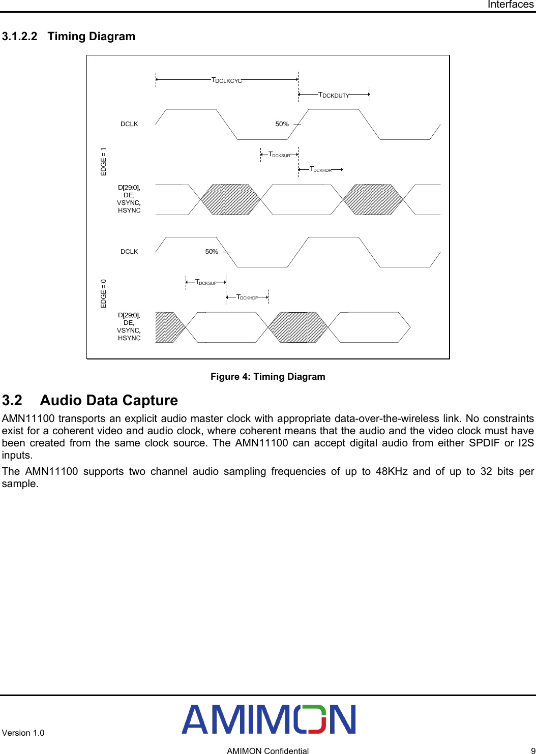
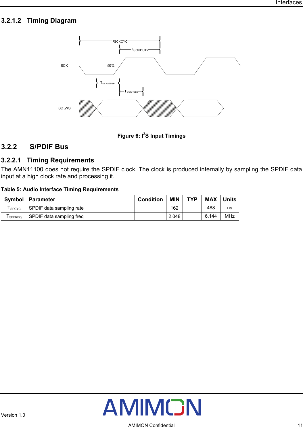
![Interfaces Common Video Input Format Table 1 describes the common supported video input resolutions. Table 1: Common Supported Video Input Resolutions Input Pixel Clock (MHz) Color Space Video Format Bus Width 480i 480p XGA 720p 1080i RGB/YCbCr 4:4:4 24 27 27 65 74.25 74.25 3.1.1 Video Channel Mapping The 30 bit video input signals are mapped to the RGB and YCbCr color space according to the options described in the following table: Table 2: Video Channel Mapping Option D[29:20] D[19:10] D[9:0] #1 RED (Cr) GREEN (Y) BLUE (Cb) #2 RED (Cr) BLUE (Cb) GREEN (Y) #3 GREEN (Y) RED (Cr) BLUE (Cb) #4 GREEN (Y) BLUE (Cb) RED (Cr) #5 BLUE (Cb) RED (Cr) GREEN (Y) #6 BLUE (Cb) GREEN (Y) RED (Cr) The AMN11100 allows any of the input video channels options. The first option is the default from power-up. In order to change the video channel mapping, please refer to the appropriate programmer's reference guide. 3.1.2 Video Interface Input Timing Diagram 3.1.2.1 Timing Requirements Important: The following parameters relate to the AMN2110 baseband chipset and not to the entire AMN11100 board. Table 3: : Video Interface Symbol Parameter MIN TYP MAX Units TDCKCYC DCLK period 12.8 40 ns TDCKFREQ DCLK frequency 25 78.125 MHz TDCKDUTY DCLK duty cycle 40% 60% ns TDCKSUR Setup time to DCLK rising edge 0.7 ns TDCKHDR Hold time to DCLK rising edge 1.1 ns TDCKSUF Setup time to DCLK falling edge 1.5 ns TDCKHDF Hold time to DCLK falling edge 0.5 ns Version 1.0 AMIMON Confidential 8](https://usermanual.wiki/Amimon/AMN11100R44/User-Guide-874468-Page-16.png)
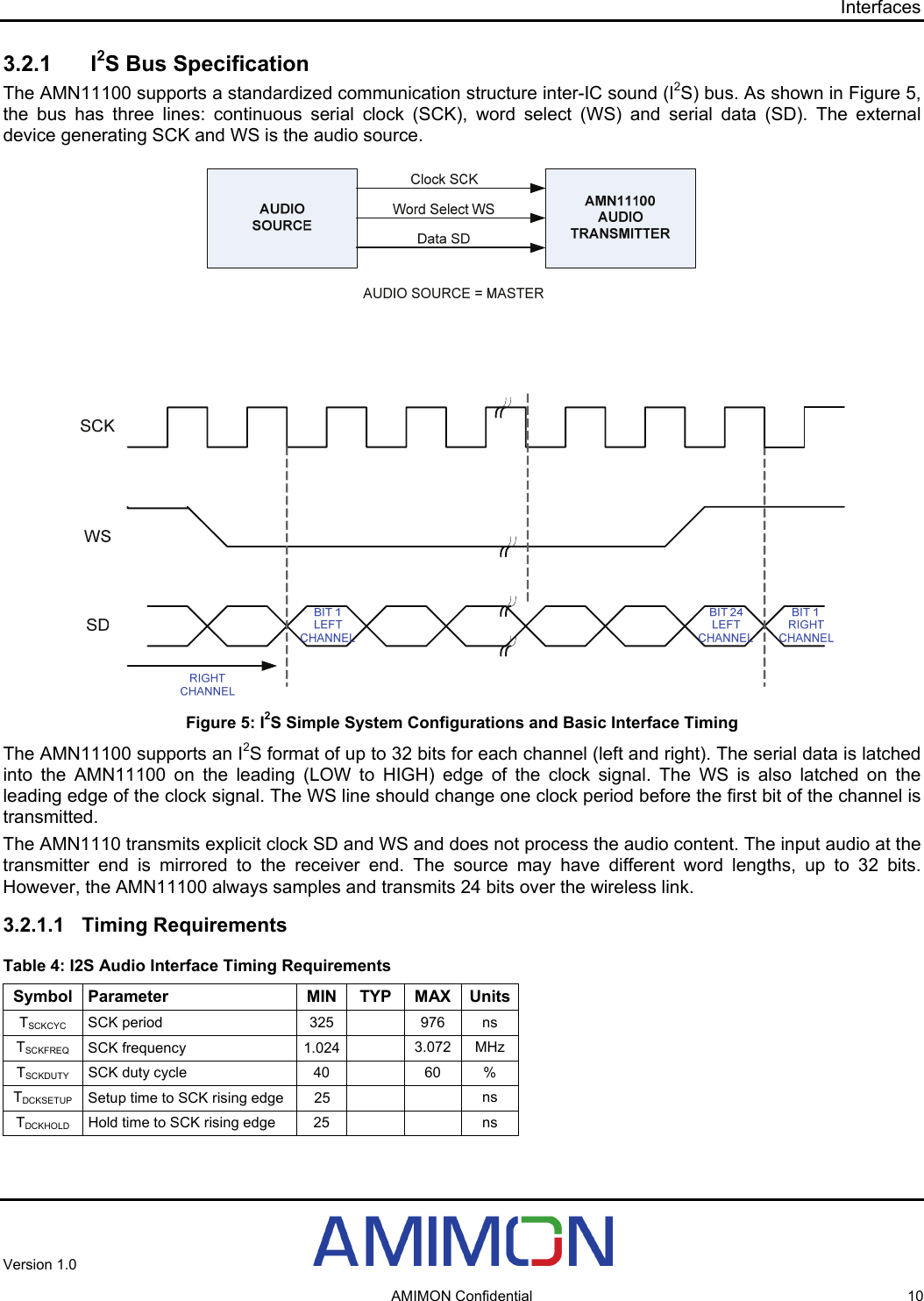
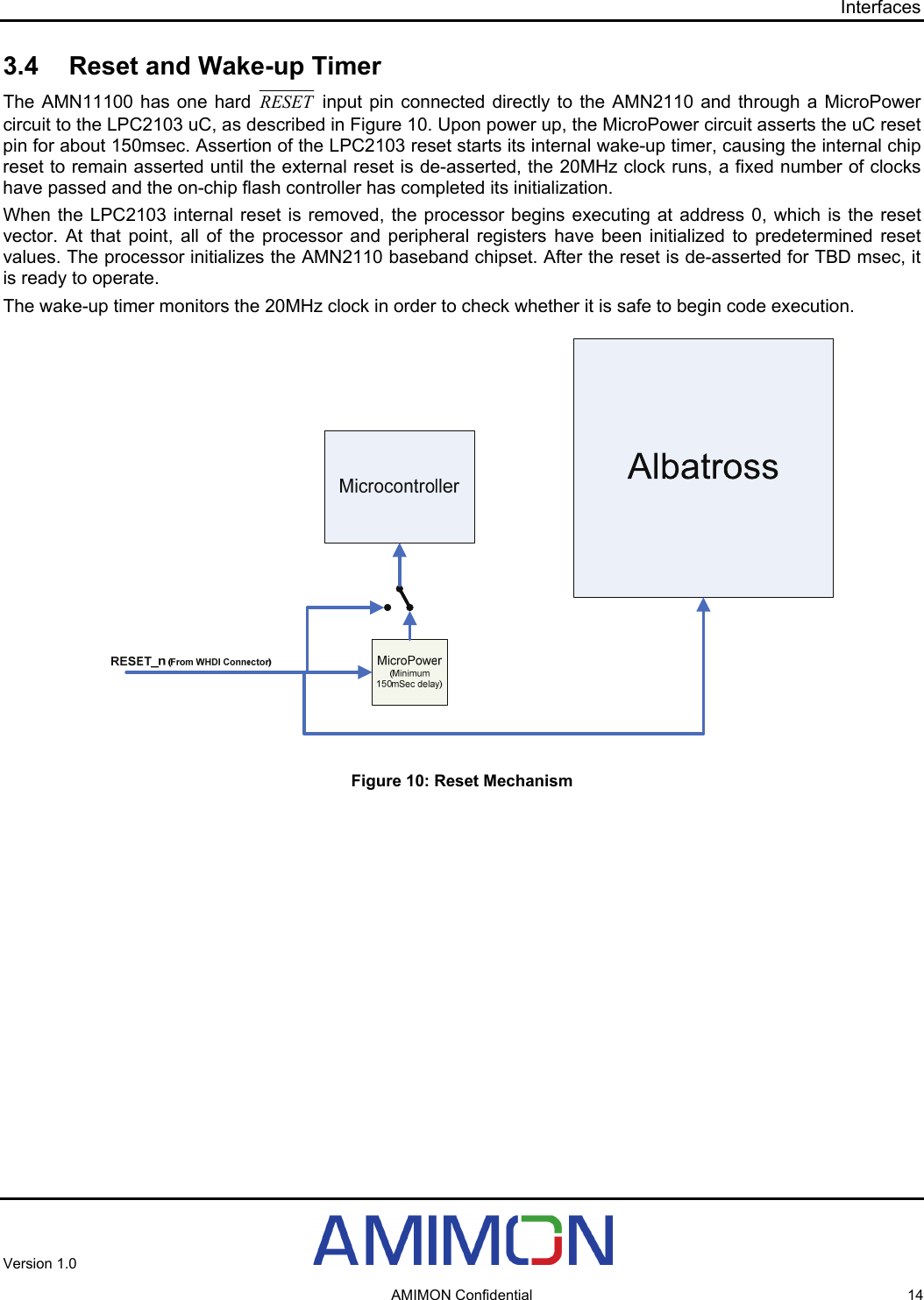
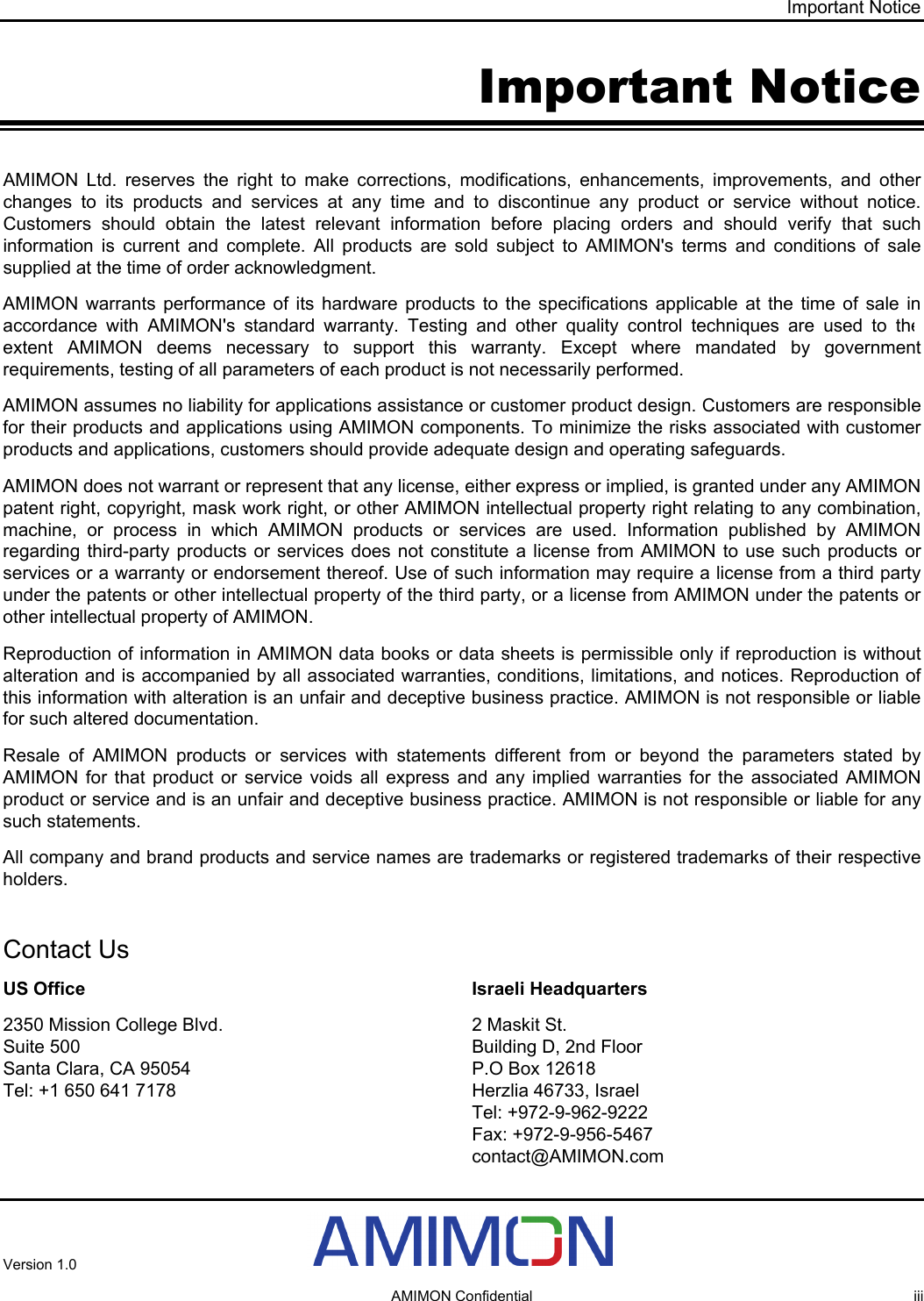
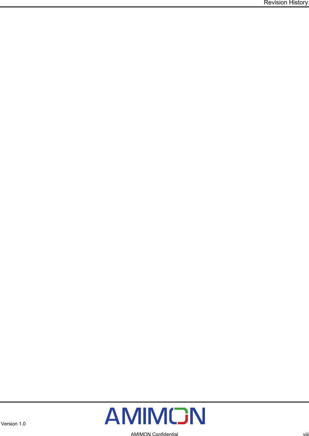
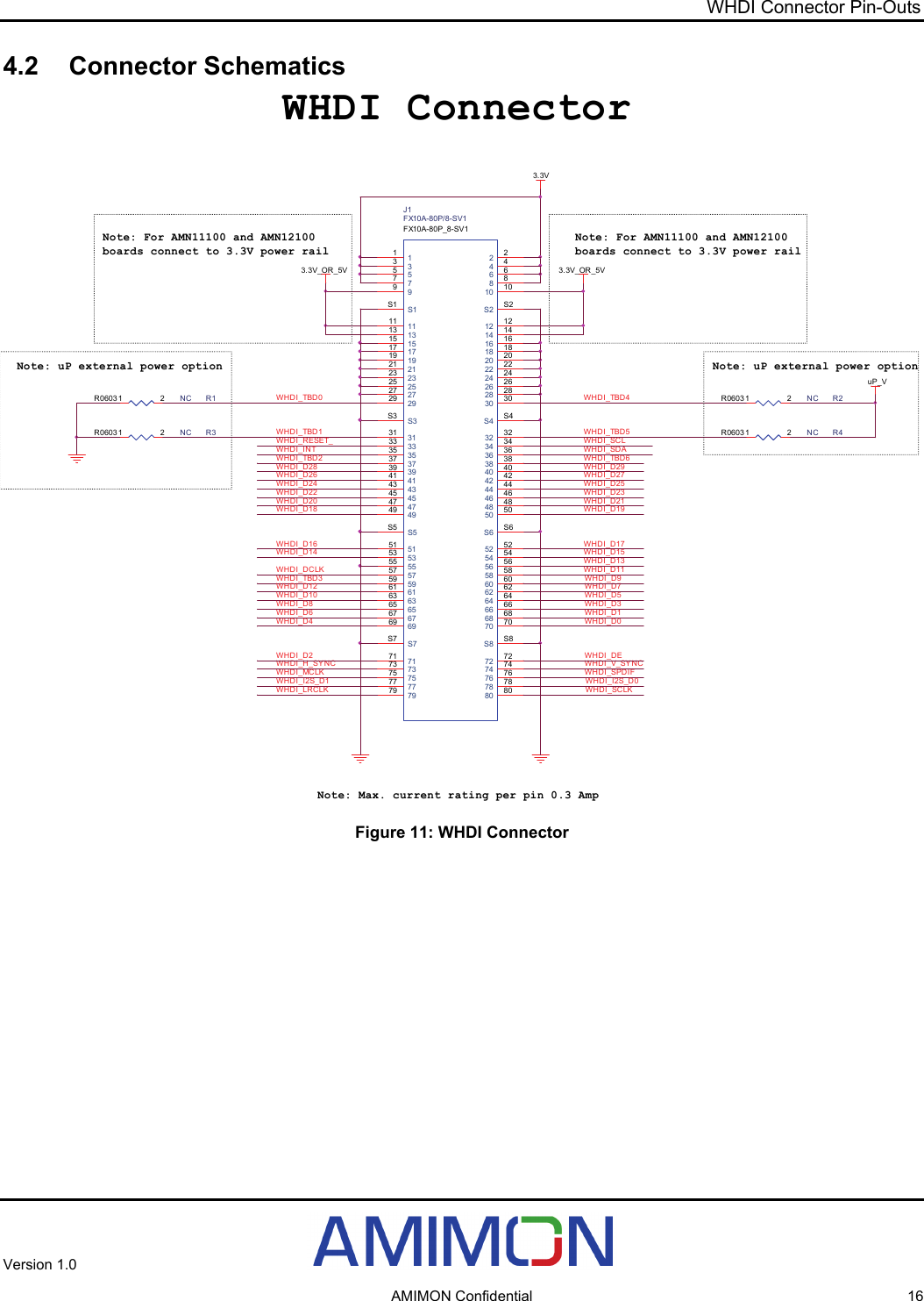
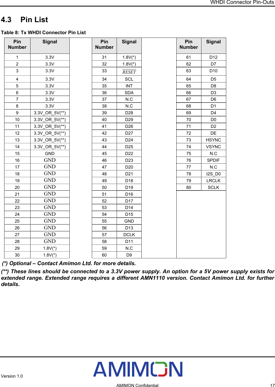
![WHDI Connector Pin-Outs Chapter 4 WHDI Connector Pin-Outs 4.1 Signals Table 7: WHDI Connector Signals Direction AMIMON Confidential 15 Remarks # of Pins Pin Name Description / Functionality Group Tx 30 D[29:0] 30-bit RGB (10:10:10) or YCrCb (10:10:10) Video In 1 DCLK Video data clock Video In Up to 78.125 MHz 1 DE Data enable Video In 1 H_SYNC Horizontal sync Video In 1 V_SYNC Vertical sync Video In 1 SPDIF SPDIF audio interface Audio In 1 SD I2S audio interface Serial Data signals Audio In 1 SCLK I2S continuous serial clock Audio In Up to 3.072Mbps 1 WS(LRCLK) I2S Word Select (Left/right clock) which defines also the sampling rate Audio In 1 MCLK I2S master clock coherent to WS according to specified ratio Audio NA Rate is adjustable on RX side 1 SDA Two-wire Serial Bus Data (Slave Mode) Control I/O Control I/F for WHDI 1 SCL Two-wire Serial Bus Clock (Slave Mode) Control In Control I/F for WHDI 1 INT Interrupt from WHDI module Control Out 1 RESET Reset / Power-down line Control In 1 TBD6 TBD6 NA NA 6 TBD[5:0] TBD0, TBD1, TBD4, TBD5 are reserved in AMN11100, AMN12100 as an option for external power rail to the on board uC TBD TBD 8 3.3V VCC Power Power 300 mA maximum rating per pin 6 3.3V_OR_5V High Power rail pins, In AMN11100, AMN12100 connect these power rail pins to the 3.3V power rail Power Power For board designed as "High-Power" PA connect this rail to 5V, For Rx (AMN12100) connect to 3.3V 15 GND Ground Power Power †Data in this table is preliminary. Version 1.0](https://usermanual.wiki/Amimon/AMN11100R44/User-Guide-874468-Page-23.png)
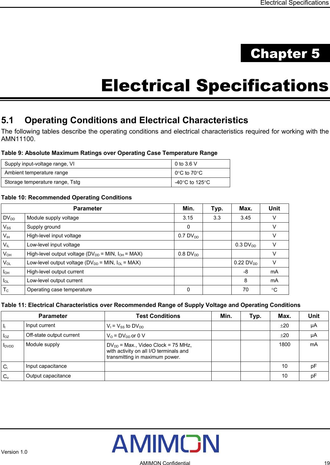
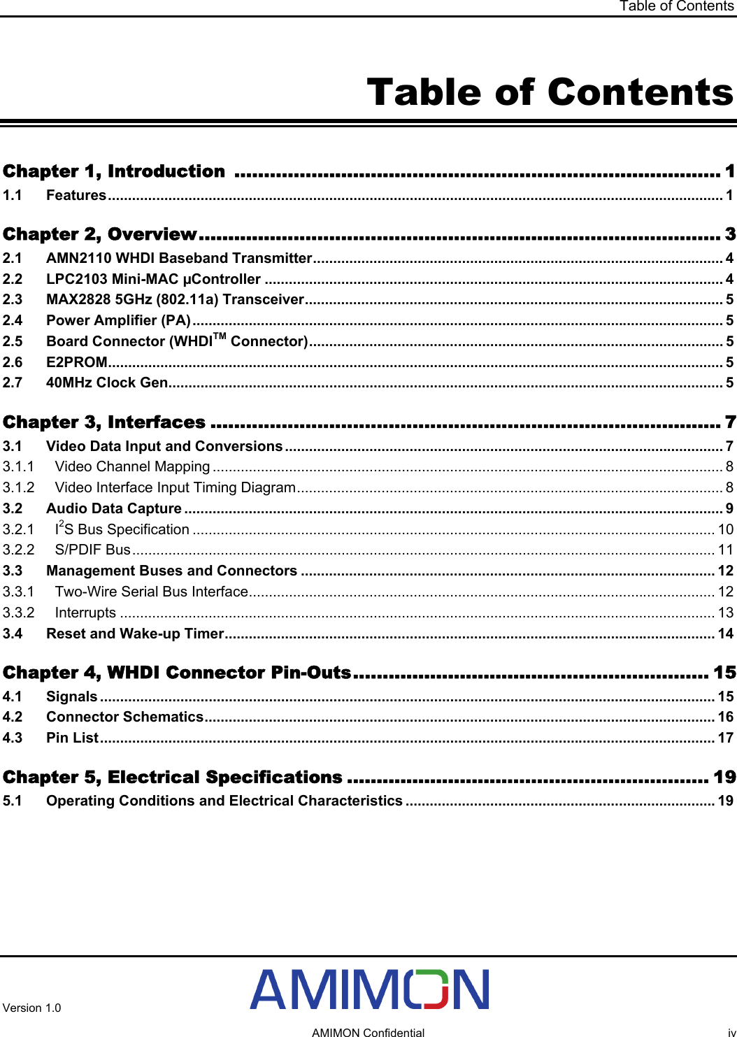
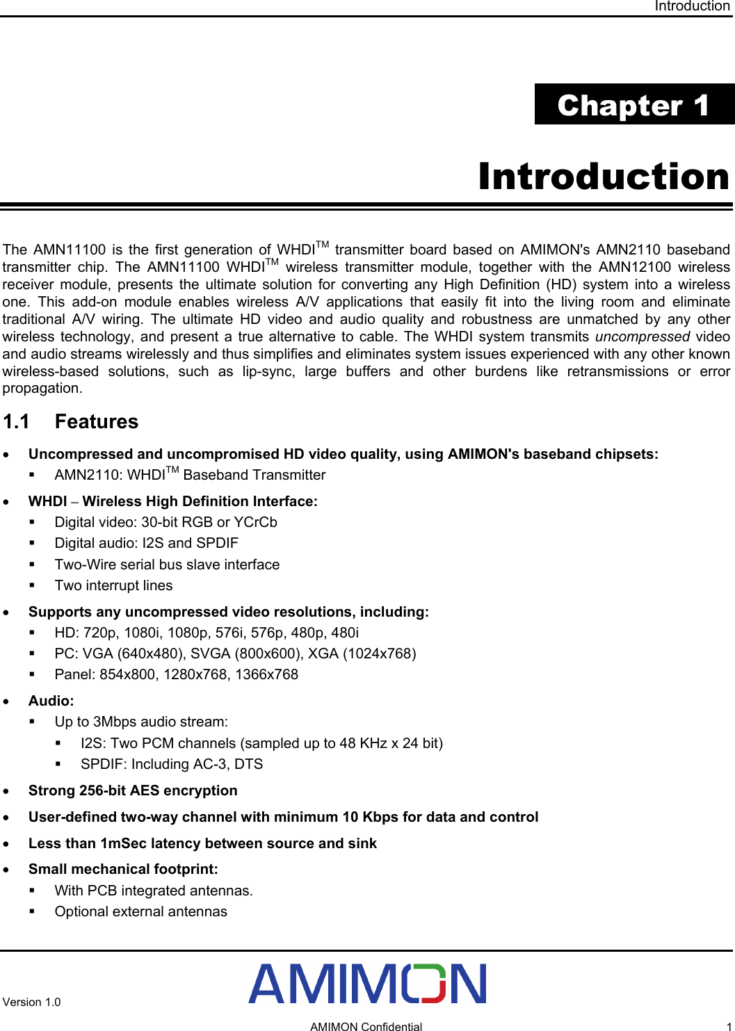
![Design Guidelines Chapter 6 Design Guidelines 6.1 Digital Layout Recommendation To better understand the layout guidelines, please refer to the AMN11100 schematics which are part of the HDK package. 6.1.1 Stuck up Recommended stuck up for 10 layers design: • Total thickness 1.6mm • Tolerance: 10% Table 12: Digital Layout Recommendation Conductor Width [mil] Control Impedance [ohm] StuckUp Before Stripline Differential thickness Scale Required Design Before Before Layer Title Des. Oz/mil Layer line space line space Required Design Required Design Type No Cu 0.5 Oz CS 5 0 5.25 5.25 0 0 100 100 SIG L1 Space 7 mil 15 30 14 31 0 0 50 48 Cu 0.5 Oz L2 11 0 12 0 50 50 0 0 GND L2 Space 4 mil 0 0 0 0 0 0 0 0 Cu 0.5 Oz L3 5 6 4.25 6.75 0 0 100 100 SIG L3 Space 7 mil 6 0 5 0 50 50 0 0 Cu 0.5 Oz L4 0 0 0 0 0 0 0 0 GND L4 Space 4 mil 0 0 0 0 0 0 0 0 Cu 0.5 Oz L5 0 0 0 0 0 0 0 0 VCC L5 Space 9 mil 0 0 0 0 0 0 0 0 Cu 0.5 Oz L6 5 6 4.5 6.5 0 0 100 100 SIG L6 Space 4 mil 6 0 5.5 0 50 50 0 0 Cu 0.5 Oz L7 0 0 0 0 0 0 0 0 GND L7 Space 7 mil 0 0 0 0 0 0 0 0 Cu 0.5 Oz L8 5 6 4.25 6.75 0 0 100 100 SIG L8 Space 4 mil 6 0 5 0 50 50 0 0 Cu 0.5 Oz L9 11 0 12 0 50 50 0 0 GND L9 Space 7 mil 15 30 14 31 0 0 50 48 Cu 0.5 Oz PS 5 0 5.25 5.25 0 0 100 100 SIG L10 Version 1.0 AMIMON Confidential 21](https://usermanual.wiki/Amimon/AMN11100R44/User-Guide-874468-Page-29.png)