Anaren A10040601 902-928 MHZ TRANSCEIVER User Manual 20170227 v1 11 11524600 A1101R09x Users Manual 2
Anaren, Inc. 902-928 MHZ TRANSCEIVER 20170227 v1 11 11524600 A1101R09x Users Manual 2
Anaren >
Contents
- 1. Users Manual
- 2. User Manual_20170227_v1 - 11_11524600 A1101R09x_Users_Manual_2
User Manual_20170227_v1 - 11_11524600 A1101R09x_Users_Manual_2


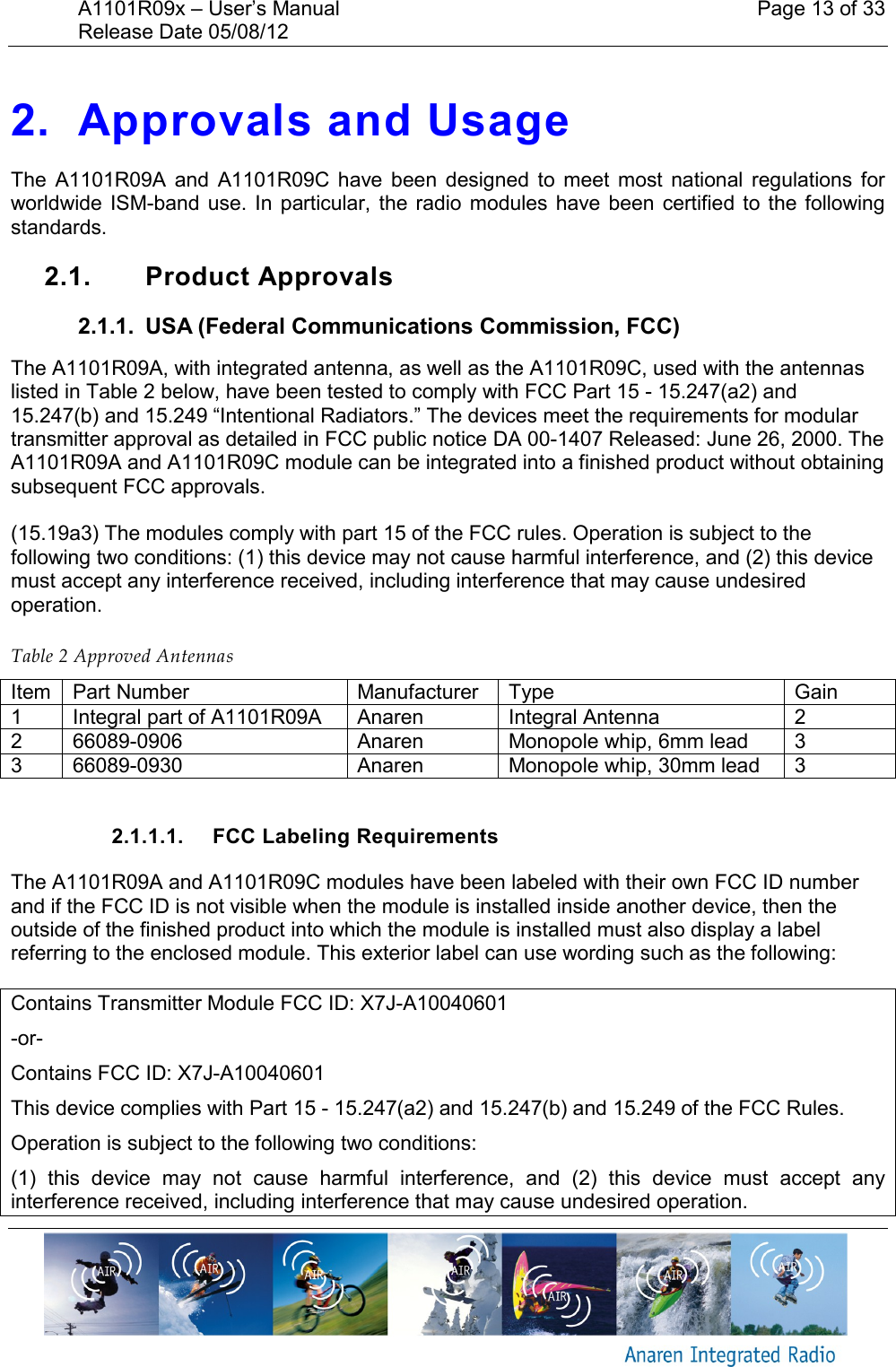
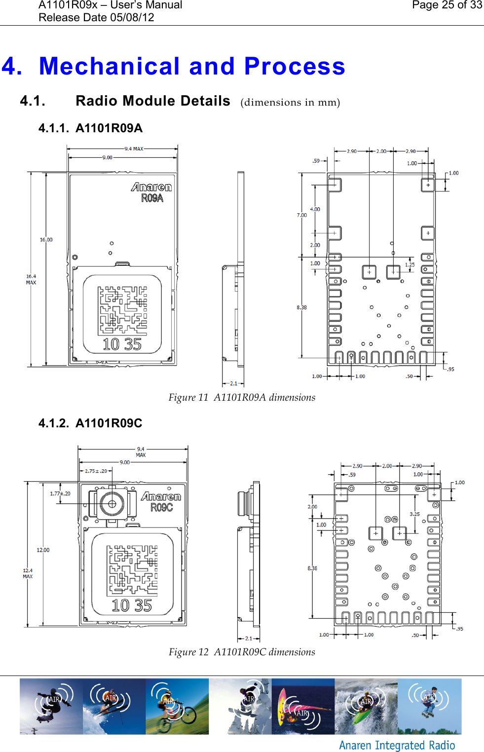
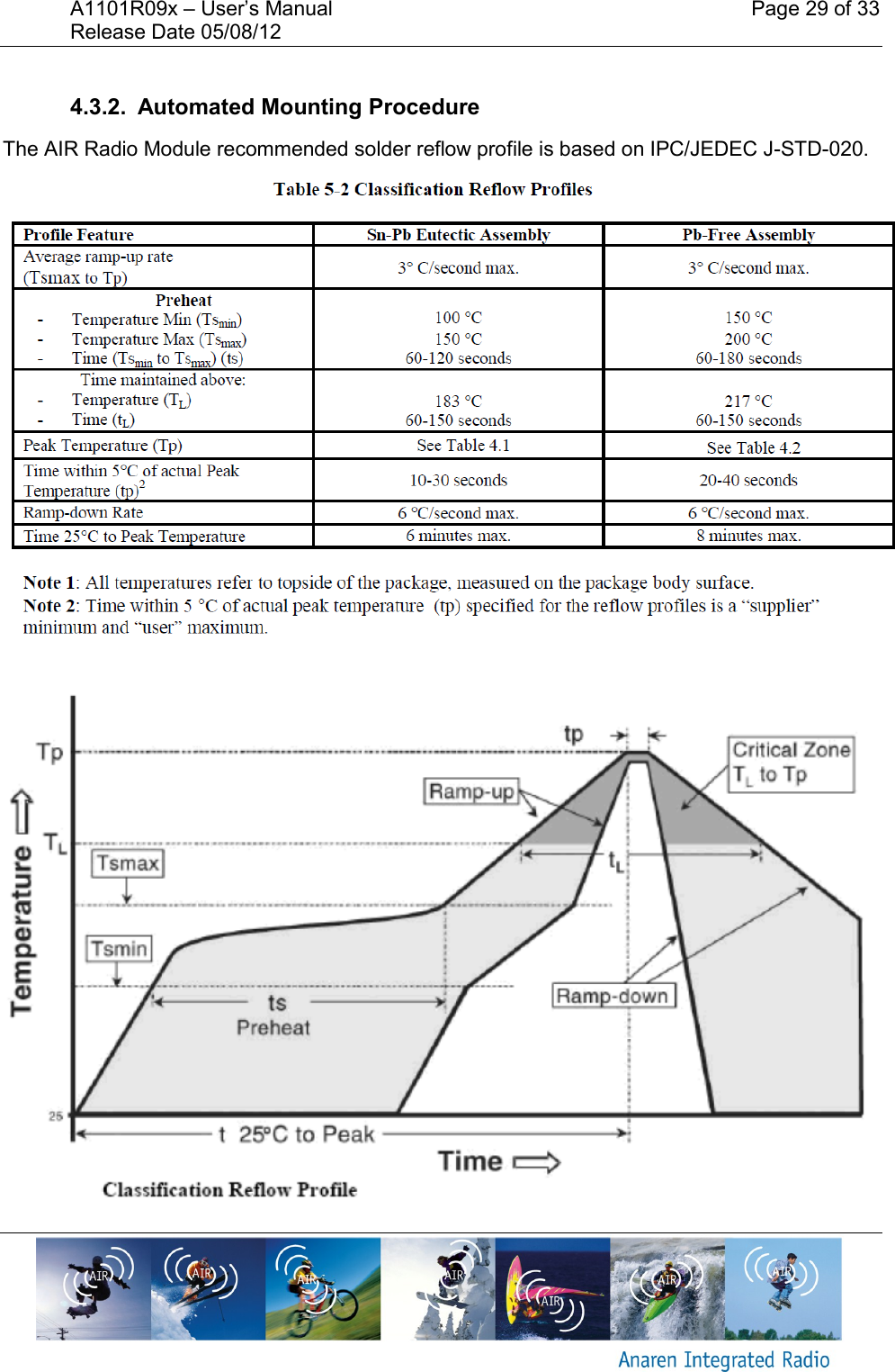
![Page 12 of 33 A1101R09x – User’s Manual Release Date 05/08/12 Table 1 Configuration Parameters Register NameRegister Address (Hex)Retained during sleep7 6 5 4 3 2 1 0IOCFG2 00 1 0 GDO2_INVIOCFG1 01 1 GDO_DS GDO1_INVIOCFG0 02 1GDO0_TEMP_SENSOR_ENABLE GDO0_INVFIFOTHR 03 1 Reserved ADC_RETENTIONSYNC1 04 1SYNC0 05 1PKTLEN 06 1PKTCTRL1 07 1 0 CRC_AUTOFLUSH APPEND_STATUSPKTCTRL0 08 1 0 WHITE_DATA 0 CRC_ENADDR 09 1CHANNR 0A 1FSCTRL1 0B 1 0FSCTRL0 0C 1FREQ2 0D 1FREQ1 0E 1FREQ0 0F 1MDMCFG4 10 1MDMCFG3 11 1MDMCFG2 12 1DEM_DCFILT_OFF MANCHESTER_ENMDMCFG1 13 1 FEC_ENMDMCFG0 14 1DEVIATN 15 1 0 0MCSM2 16 1 RX_TIME_RSSI RX_TIME_QUALMCSM1 17 1MCSM0 18 1 PIN_CTRL_EN XOSC_FORCE_ONFOCCFG 19 1FOC_BS_CS_GATE FOC_POST_KBSCFG 1A 1 BS_POST_K BS_POST_KPAGCCTRL2 1B 1AGCCTRL1 1C 1 0 AGC_LNA_PRIORITYAGCCTRL0 1D 1WOREVT1 1E 1WOREVT0 1F 1WORCTRL 20 1 RC_PD RC_CAL 0FREND1 21 1FREND0 22 1 0FSCAL3 23 1FSCAL2 24 1VCO_CORE_H_ENFSCAL1 25 1FSCAL0 26 1 0RCCTRL1 27 1 0RCCTRL0 28 1 0FSTEST 29 0PTEST 2A 0AGCTEST 2B 0TEST2 2C 0TEST1 2D 0TEST0 2E 0VCO_SEL_CAL_EN TEST0[0]2FPARTNUM 30 1VERSION 31 1FREQOFF_EST 32 0LQI 33 0CRC_OKRSSI 34 0MARC_STATE 35 0WORTIME1 36 0WORTIME0 37 0PKTSTATUS 38 0CRC_OK CS PQT_REACHED CCA SFD GDO2 GDO0VCO_VC_DAC 39 0TXBYTES 3A 0TXFIFO_UNDERFLOWRXBYTES 3B 0RXFI FO_OVERFLOWRCCTRL1_STATUS 3C 0RCCTRL0_STATUS 3D 0PATABLE 3E 1FIFO 3F 0Bit Fields Within RegisterSYNC_LSBPACKET_LENGTHPQTADR_CHKPKT_FORMATLENGTH_CONFIGGDO2_CFGGDO1_CFGGDO0_CFGCLOSE_IN_RXFIFO_THRSYNC_MSBFREQ[15:8]FREQ[7:0]CHANBW_ECHANBW_MDRATE_EDRATE_MDEVICE_ADDRCHAN0FREQ_IFFREQOFFFREQ[23:22]=0FREQ[21:16]DEVIATION_EDEVIATION_M0RX_TIME0CCA_MODERXOFF_MODETXOFF_MODEMOD_FORMATSYNC_MODENUM_PREAMBLE0CHANSPC_ECHANSPC_MBS_PRE_KBS_PRE_KPBS_LIMITMAX_DVGA_GAINMAX_LNA_GAINMAGN_TARGET0FS_AUTOCALPO_TIMEOUT0FOC_PRE_KFOC_LIMITEVENT0[15:8]EVENT0[7:0]EVENT1WOR_RESLNA_CURRENTLNA2MIX_CURRENTLODIV_BUF_CURRENTMIX_CURRENTCARRIER_SENSE_REL_THRCARRIER_SENSE_ABS_THRHYST_LEVELWAIT_TIMEAGC_FREEZEFILTER_LENGTH0FSCAL20FSCAL1FSCAL0RCCTRL10LODIV_BUF_CURRENT_TXPA_POWERFSCAL3[7:6]CHP_CURR_CAL_ENFSCAL3[3:0]TEST0[7:2]PARTNUMVERSIONFREQOFF_ESTLQI_ESTRSSIRCCTRL0FSTESTPTESTAGCTESTTEST2TEST1NUM_RXBYTESRCCTRL1_STATUSRCCTRL0_STATUSPATABLETXFIFO/RXFIFOMARC_STATETIME[15:8]TIME[7:0]VCO_VC_DACNUM_TXBYTES](https://usermanual.wiki/Anaren/A10040601.User-Manual-20170227-v1-11-11524600-A1101R09x-Users-Manual-2/User-Guide-3355953-Page-12.png)