Anaren A10051702 2400 - 2483.5 MHz Transceiver User Manual
Anaren, Inc. 2400 - 2483.5 MHz Transceiver
UserManual.wiki
>
Anaren
>
A10051702 User Manual
>
User Manual
Contents
1.
User Manual
2.
Manual
User Manual
Navigation menu
Upload a User Manual
Namespaces
Wiki Guide
HTML
PDF
Info
Views
User Manual
Discussion / Help
Navigation

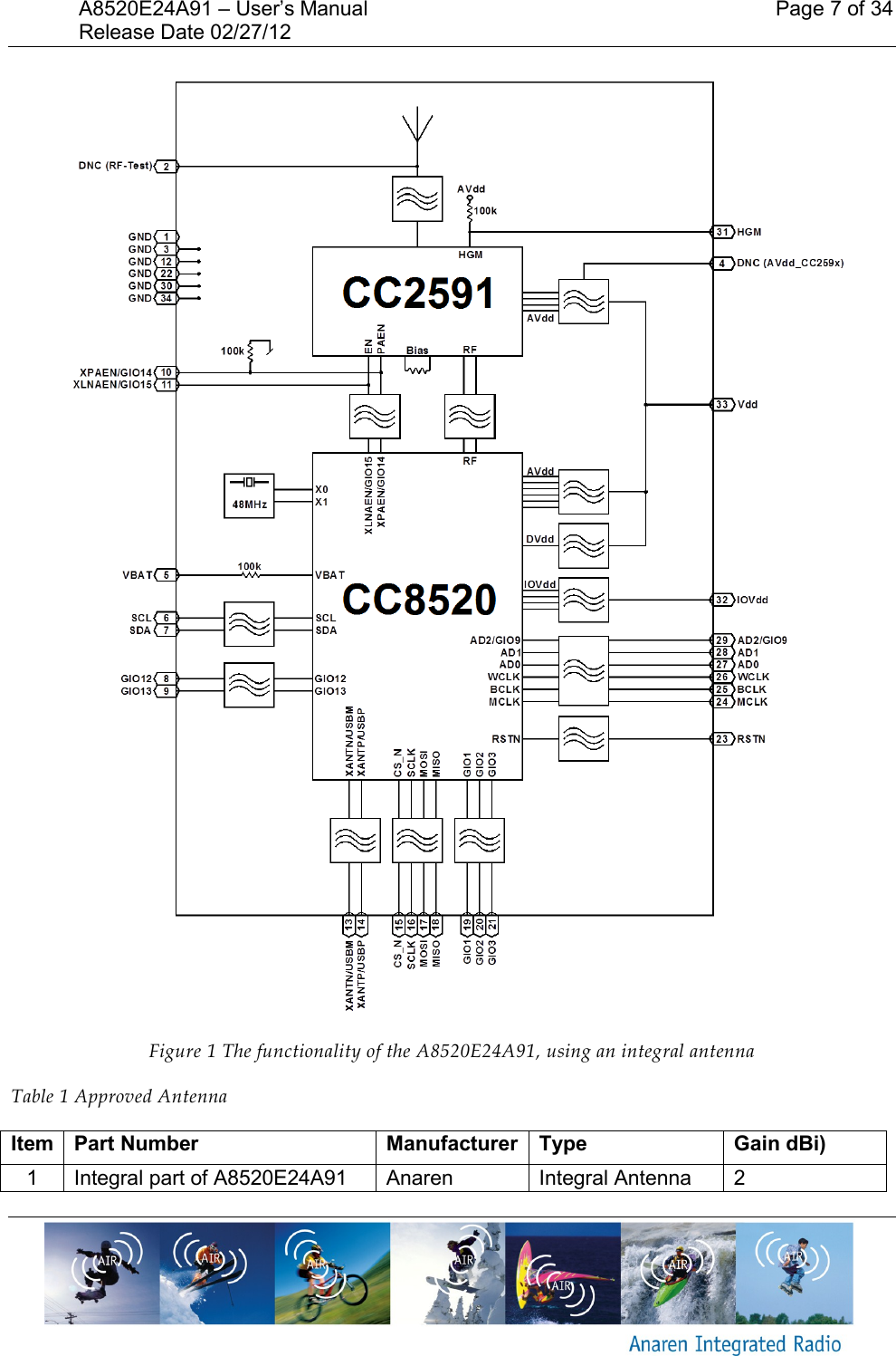
![Page 10 of 34 A8520E24A91 – User’s Manual Release Date 02/27/12 Figure 3 Example of AFH hop sequence (active set in color, trial set in black/gray) The channels correspond to center frequencies as given in Table 2. Table 2 Channel to center frequency Channel Center Frequency [MHz] Channel Center Frequency [MHz] 1 2406 10 2442 2 2410 11 2446 3 2414 12 2450 4 2418 13 2454 5 2422 14 2458 6 2426 15 2462 7 2430 16 2466 8 2434 17 2470 9 2438 18 2474 1.3. Applications Wireless headphones Wireless headsets Wireless speakers Wireless studio equipment Wireless microphones](https://usermanual.wiki/Anaren/A10051702.User-Manual/User-Guide-1650044-Page-10.png)


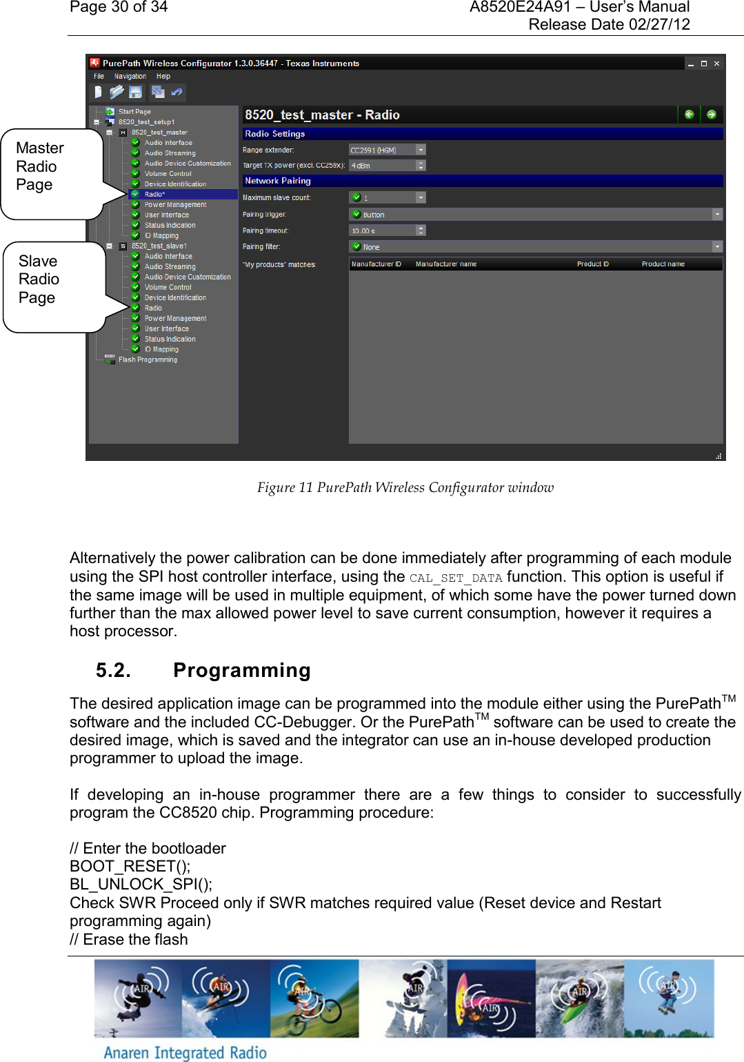
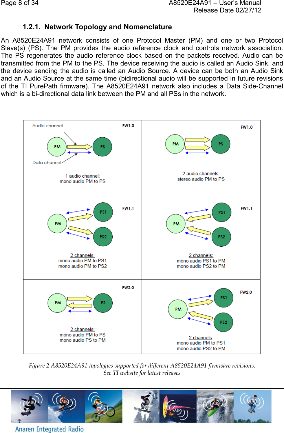
![A8520E24A91 – User’s Manual Page 29 of 34 Release Date 02/27/12 5. Configuration and Programming The integrator of this module into an application must program the module to match both the Codec chip used and the human interface methods employed. To do this the integrator must use the PurePath™ software from TI to configure the module 5.1. Calibrating Transmit Power This power calibration number is an approximate power output value in dBm for the CC85xx chip – however the module CC2591 adds additional 16dB amplification. It can be useful to set a lower power for systems that do not require the full range and thus save on power consumption. The typical power consumption at 3.3v supply for a A8520E24A91 module is shown below depending on the output power setting. Table 6 Transmit power settings PurePath Power Setting Module Output Power (Approximate) Peak Current Consumption Average Current Consumption [mA] @ 3.3V AVdd,IOVdd, Ambient* [dBm] [dBm] [dBm] Master Slave 4 20 184 78 36 3 19 174 72 35 2 17 147 64 34 1 15 143 63 34 0 13 118 55 32 -1 13 118 54 32 -2 12 113 52 32 -3 11 106 50 32 -4 11 106 50 32 -5 10 99 48 31 -6 10 97 47 31 -7 10 97 47 31 -8 8 94 46 31 -9 7 92 46 31 -10 6 91 46 31 * PurePath application state set to “stereo audio” In the PurePathTM configurator when creating the application image, in the “Radio” page for both master and slave the target Tx power must be set to the max allowed power level, or lower, (note that the max allowed power setting for US and Canada is 4. However for Europe, only the power settings up to -3 are allowed due to power spectral density limits). Figure 11 indicates the location for setting the module output power. PurePath Wireless Configurator 1.3.0.36447 has been used for the current measurements.](https://usermanual.wiki/Anaren/A10051702.User-Manual/User-Guide-1650044-Page-29.png)