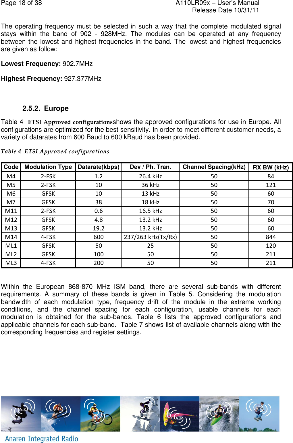
Anaren A11072401 902-928 MHZ TRANSCEIVER User Manual
Anaren, Inc. 902-928 MHZ TRANSCEIVER Users Manual
UserManual.wiki
>
Anaren
>
A11072401 User Manual
>
Users_Manual
Contents
1.
Users_Manual
2.
User Manual
Users_Manual
Navigation menu
Upload a User Manual
Namespaces
Wiki Guide
HTML
PDF
Info
Views
User Manual
Discussion / Help
Navigation


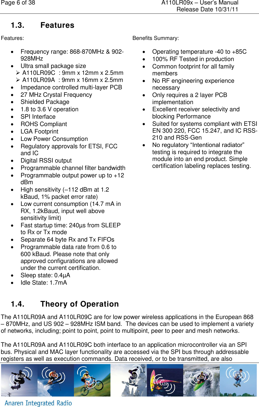
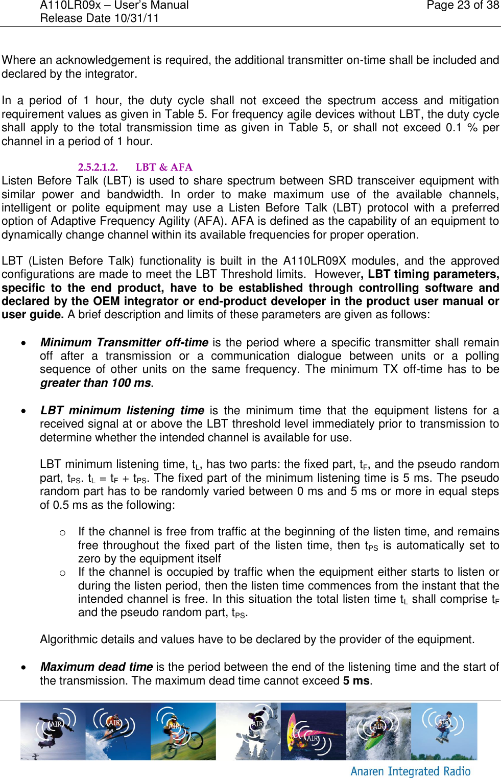
![A110LR09x – User’s Manual Page 17 of 38 Release Date 10/31/11 2.5.1. US & Canada Within the US and Canada, the modules have been approved for use as digitally modulated transmitters. In the US, the occupied bandwidth (6dB BW) should be greater than 500 kHz, whereas in Canada, the max BW (99% BW) should be 0.5% of the center frequency. Table 2 shows the configurations that have been approved for use both in the US and Canada. Table 2 FCC/IC Approved Configurations Code Modulation Type Datarate(kbps) Deviation (kHz) Max Output Power(dBm[Hex])ML4 2-FSK 1.2 237 7 [0xCD]ML5 2-FSK 38.4 237 8 [0xCA]ML6 2-FSK 100 237 10 [0xC4]ML7 2-FSK 250 237 12 [0xC0] Due to FCC power spectral density requirements, the output power must be limited by the given value for each modulation types. The given hex value in Table 2 represents the PA Table setting for the module to ensure the correct maximum output power. Table 3 gives a list of available output powers that the module has along with the corresponding PA Table register values. Table 3 Output Power vs. PA Table Value Power (dBm) PA_Table(Hex) Power (dBm) PA_Table(Hex) 12 0xC0 4.2 0x84 11 0xC1 4 0x85 10.5 0xC2 3.6 0x86 10.3 0xC3 3.4 0xCF 10 0xC4 3 0x88 9.6 0xC5 2.5 0x8A 9.2 0xC6 2 0x8B 9 0xC7 1 0x8D 8.6 0xC8 0 0x8E 8.2 0xC9 -0.5 0x70 8 0xCA -1 0x60 7.6 0xCB -2 0x40 7.2 0xCC -2.2 0x62 7 0xCD -5 0x67 6.2 0xCE -10 0x6D 5 0x80 -15 0x24 4.8 0x81 -20 0x22 4.6 0x82 -25 0x14 4.4 0x83 -30 0x03](https://usermanual.wiki/Anaren/A11072401.Users-Manual/User-Guide-1573975-Page-17.png)
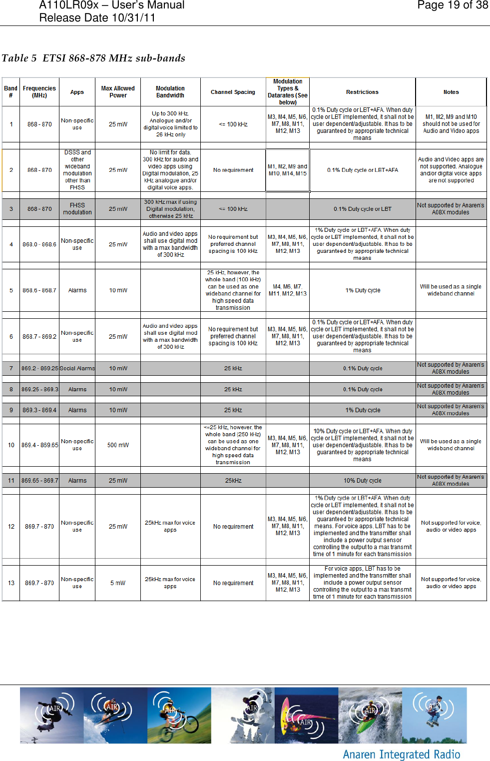
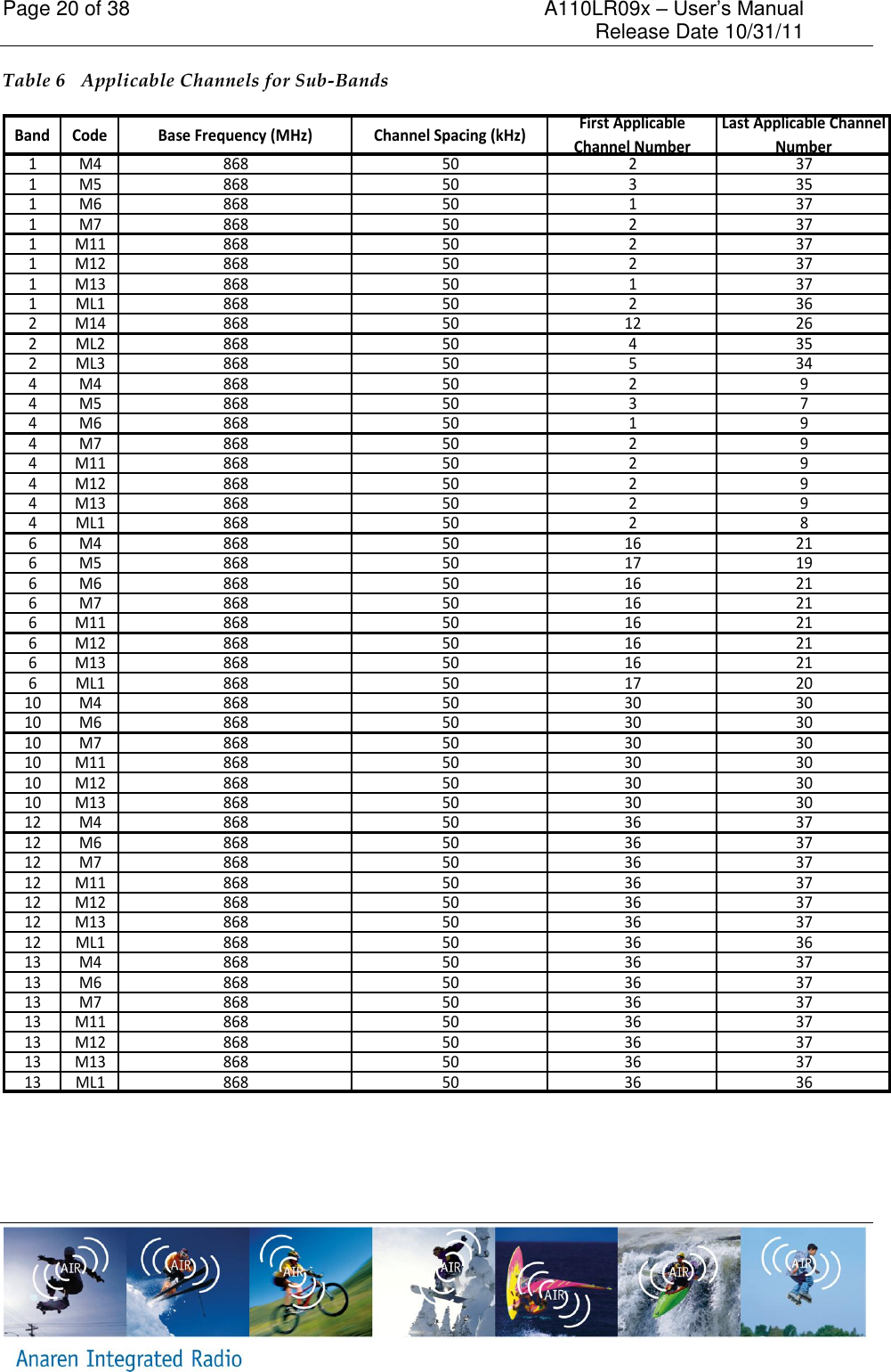
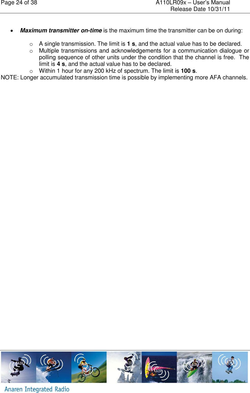
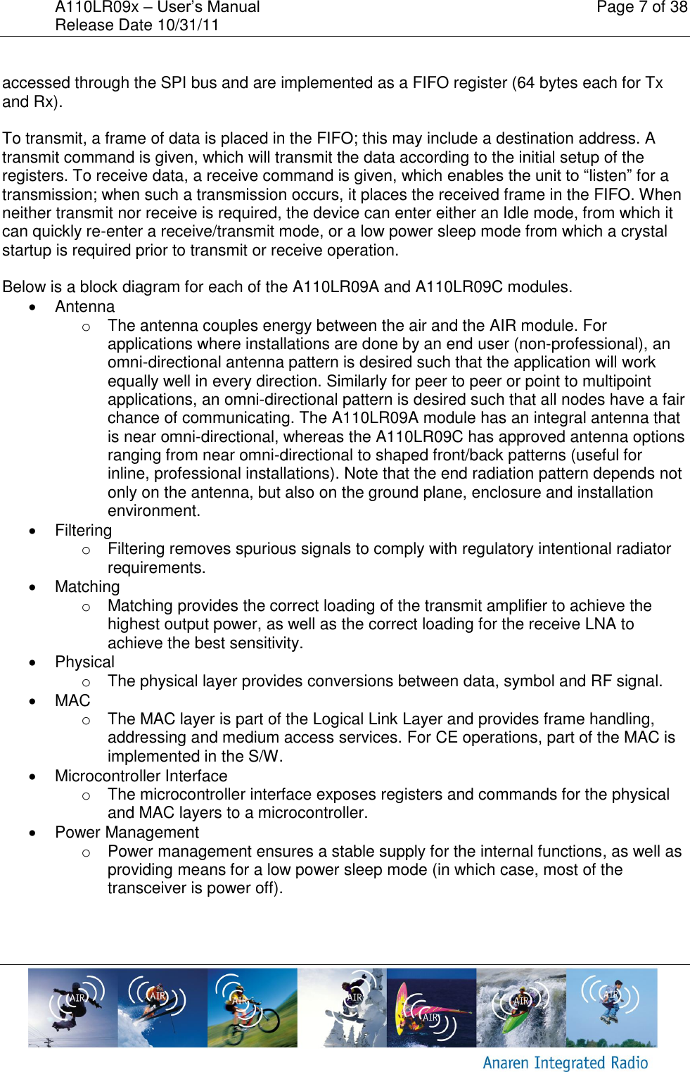
![Page 22 of 38 A110LR09x – User’s Manual Release Date 10/31/11 In order to comply with the output power limitations in Europe, the maximum values given in Table 8 below must be observed. Modulations M14, ML2 and ML3 are considered to be wideband modulations and therefore subject to the power spectral density requirements. Lower power levels for these configurations ensure compliance to the specifications. The limits are given based on the maximum allowed power level in a specific band and temperature conditions. Table 8 CW Output Powers Low Temp Power (dBm[Hex]) Normal Temp Power (dBm[Hex]) High Temp Power (dBm[Hex])14 dBm Limit 12 (C0) 12 (C0) 12 (C0)10 dBm Limit 8.6 (C8) 9.6 (C5) 10 (C4)7 dBm Limit 4.6 (82) 6.2 (CE) 7 (CD)M14 4.4 (83) 6.2 (CE) 7 (CD)ML2 -2 (40) 0 (8E) 1 (8D)ML3 -2 (40) -1 (60) 0 (8E) 2.5.2.1. Spectrum Access and Mitigation Requirements As part of the requirements for compliance, the applications must observe the restrictions that are listed in Table 5. Specifically, the spectrum access and mitigation requirements (e.g. Duty Cycle or LBT+AFA) have to be met. Some sub-bands (see Table 5) allow limited Duty cycling while some others let the user choose between limited Duty cycling and LBT+AFA implementation. In case of LBT+AFA, AFA (Adaptive Frequency Agility) has to be implemented in the customer’s SW stack since there is no specific hardware support for this functionality. 2.5.2.1.1. Duty Cycling Table 5 lists all sub-bands together with the usage requirements. In this table, Duty Cycling requirements are listed under “Restrictions” column. It applies to all transmitters excluding those with a LBT facility with AFA (explained in the next sub-section). The Duty Cycle is defined as the ratio, expressed as a percentage, of the maximum transmitter “ON” time monitored over one hour, relative to a one hour period. The device may be triggered either automatically or manually. And, depending on how the device is triggered, the duty cycle is either fixed or random. For automatic operated devices, either software controlled or pre-programmed devices, the OEM integrator or end product developer shall declare the duty cycle class or classes in the end-product user manual or user guide. For manual operated or event-dependent devices, with or without software controlled functions, the integrator shall declare whether the device once triggered, follows a pre-programmed cycle, or whether the transmitter remains on until the trigger is released or the device is manually reset. The integrator shall also give a description of the application for the device and include a typical usage pattern. The typical usage pattern as declared by the integrator shall be used to determine the duty cycle and hence the duty class.](https://usermanual.wiki/Anaren/A11072401.Users-Manual/User-Guide-1573975-Page-22.png)