AnyDATA DT2000DUAL CDMA Wireless Data Modem, EMIII-Dual User Manual EMIII Dual service manual
AnyDATA Corporation CDMA Wireless Data Modem, EMIII-Dual EMIII Dual service manual
AnyDATA >
Contents
- 1. Users Manual
- 2. Service Manual
Service Manual
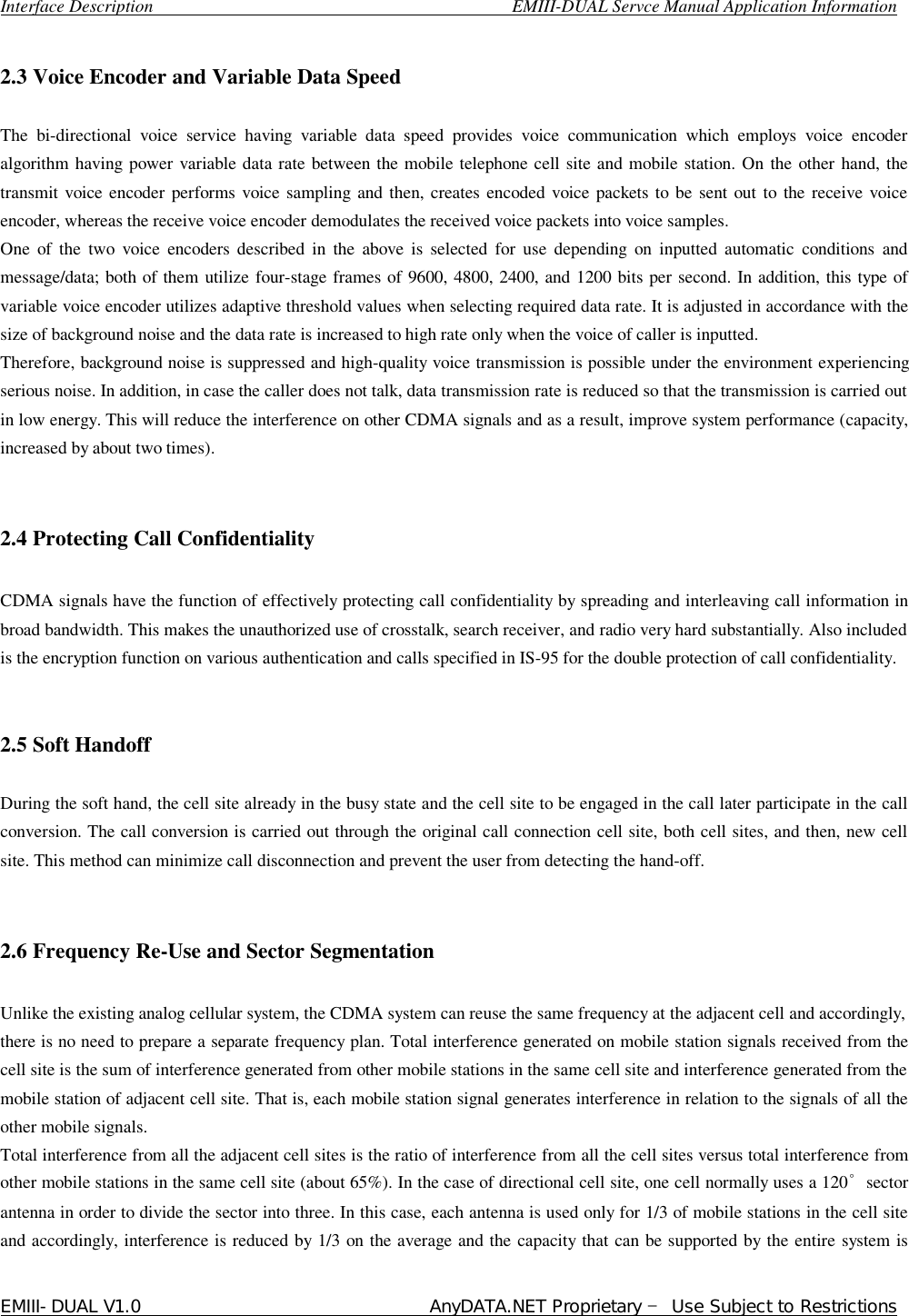
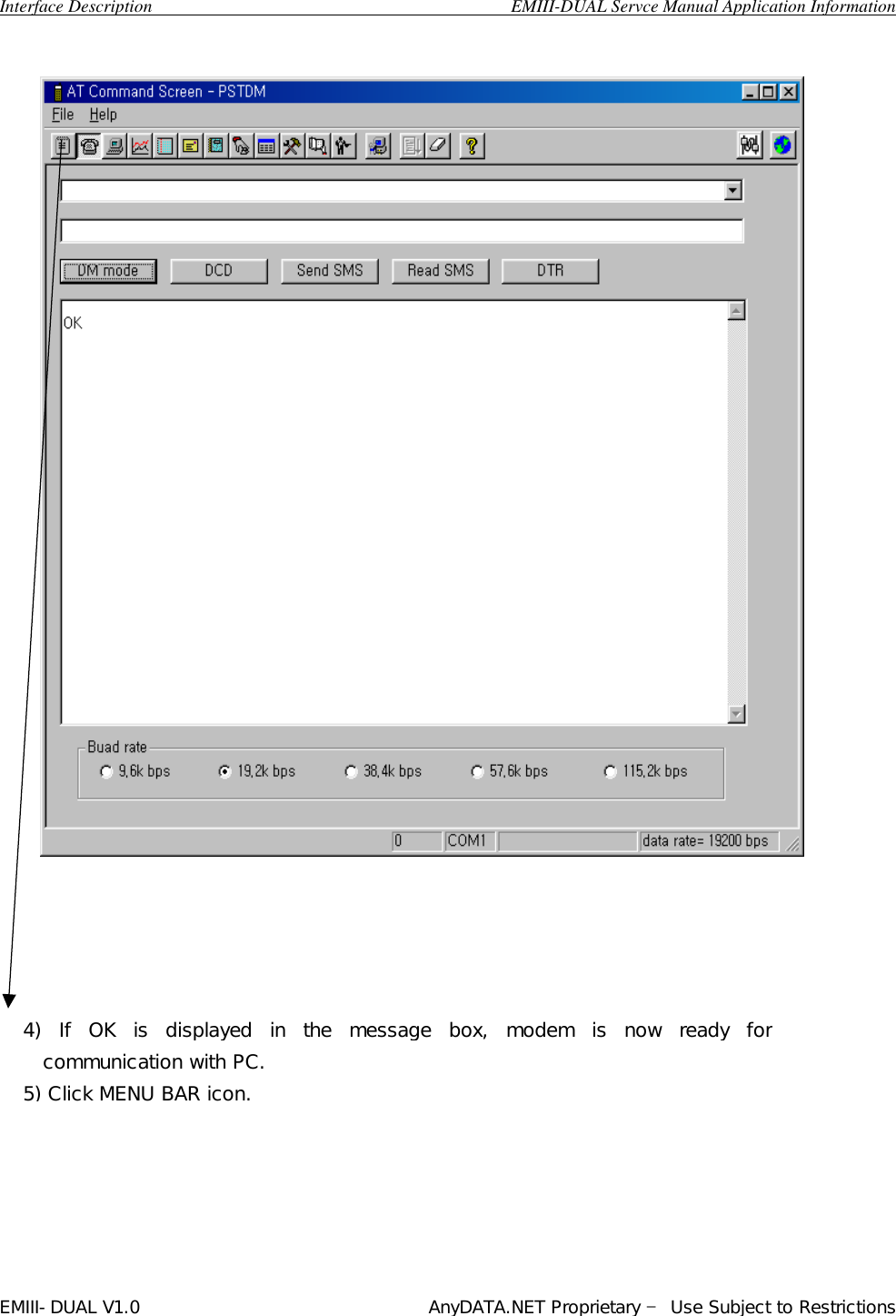
![Interface Description EMIII-DUAL Servce Manual Application Information EMIII-DUAL V1.0 AnyDATA.NET Proprietary – Use Subject to Restrictions 2. OPERATION METHOD 2) Set Buad rate to the modem’s. 3) Click [DM mode] 1) Run PSTDM program at Windows95 or Windows98](https://usermanual.wiki/AnyDATA/DT2000DUAL.Service-Manual/User-Guide-242042-Page-16.png)
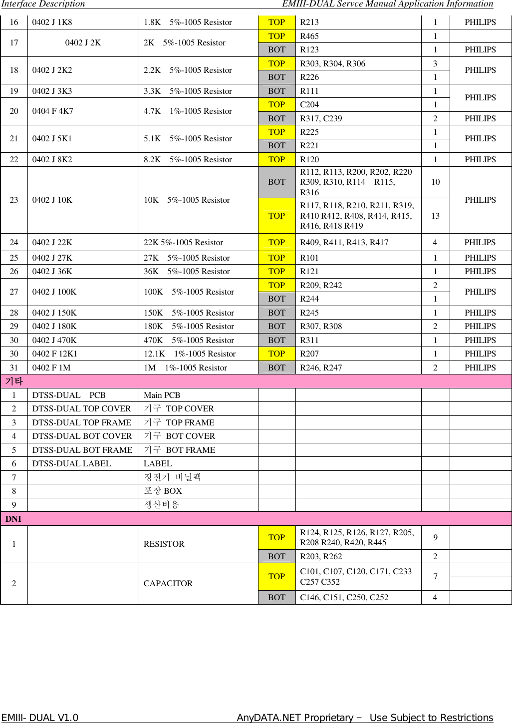
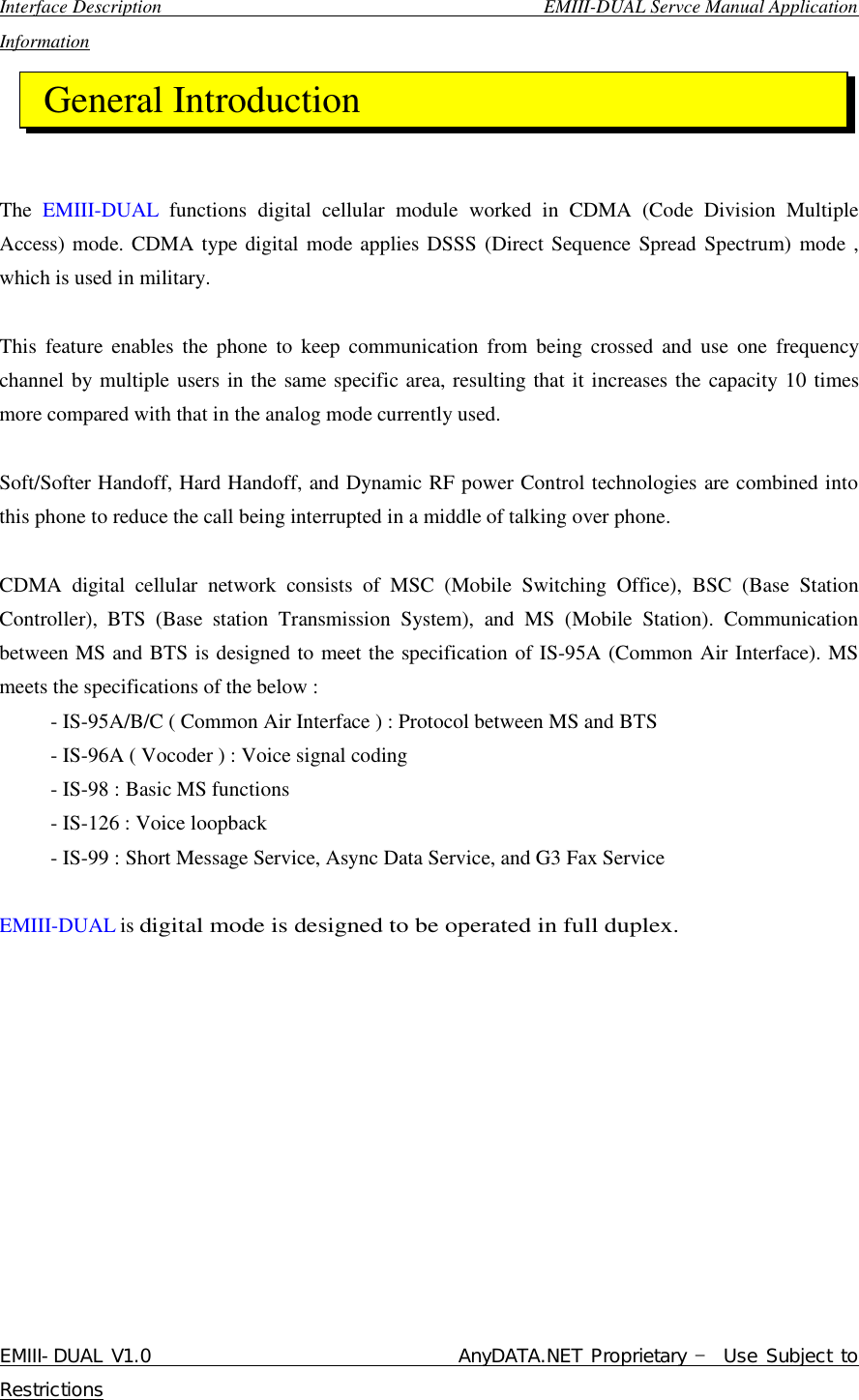
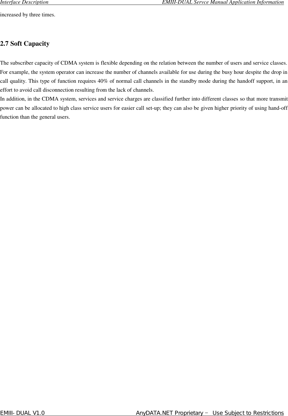
![Interface Description EMIII-DUAL Servce Manual Application Information EMIII-DUAL V1.0 AnyDATA.NET Proprietary – Use Subject to Restrictions 6) As shown in the picture above, service file input plane will be displayed (See if clock is running. If it isn’t, communication with PC is not activated. Repeat step 1 through 5, or reset the power of modem and repeat step 1 through 5) 7) Type NAM Programming script like the example shown below, <NAM Programming script example> Mode offline-d [ENTER] nv_write name_nam {0," AnyDATA telecom "} [ENTER] nv_write name_nam {1," AnyDATA telecom "} [ENTER] Mode reset [ENTER] SCRIPTINPUT WINDOW](https://usermanual.wiki/AnyDATA/DT2000DUAL.Service-Manual/User-Guide-242042-Page-18.png)
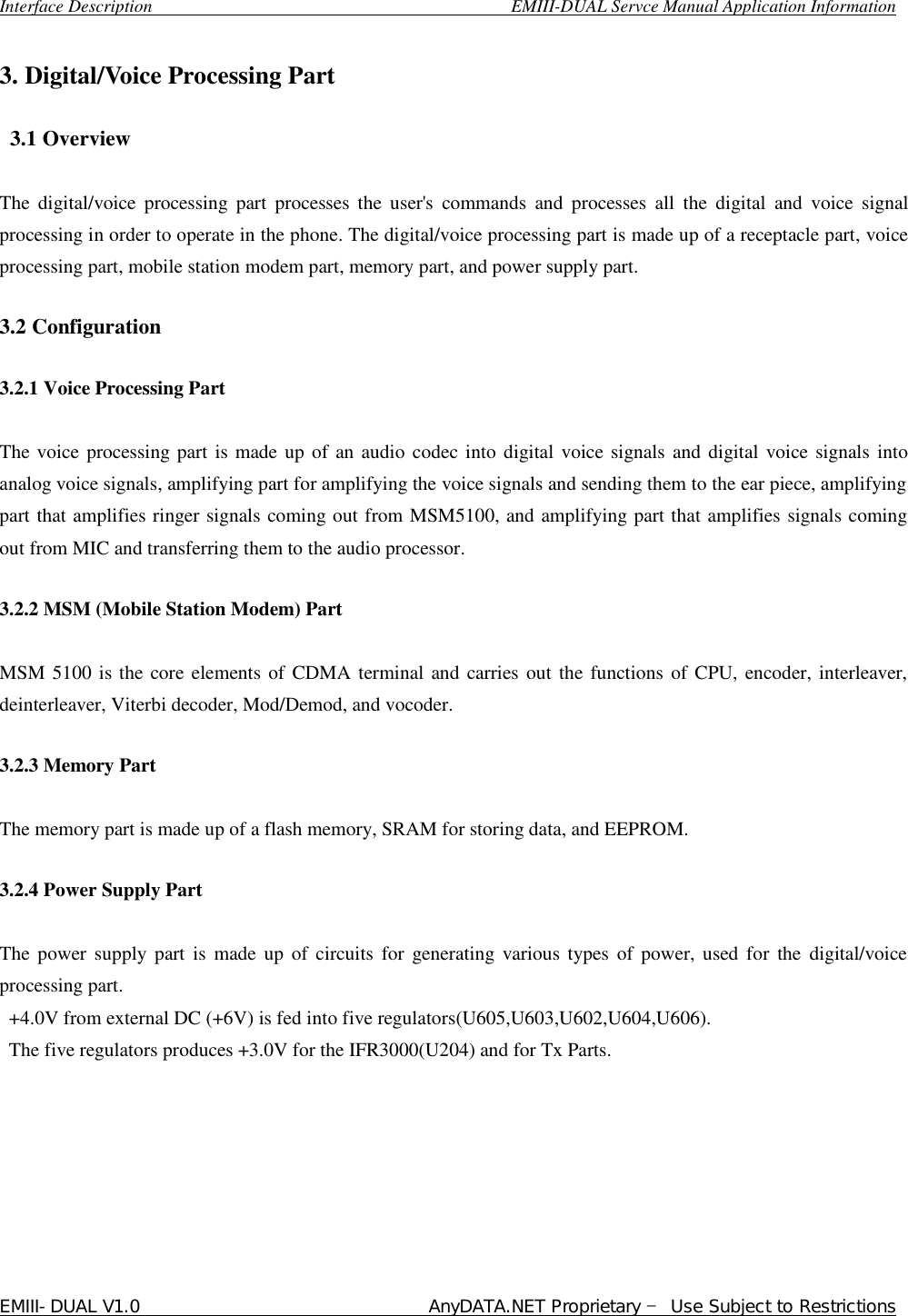
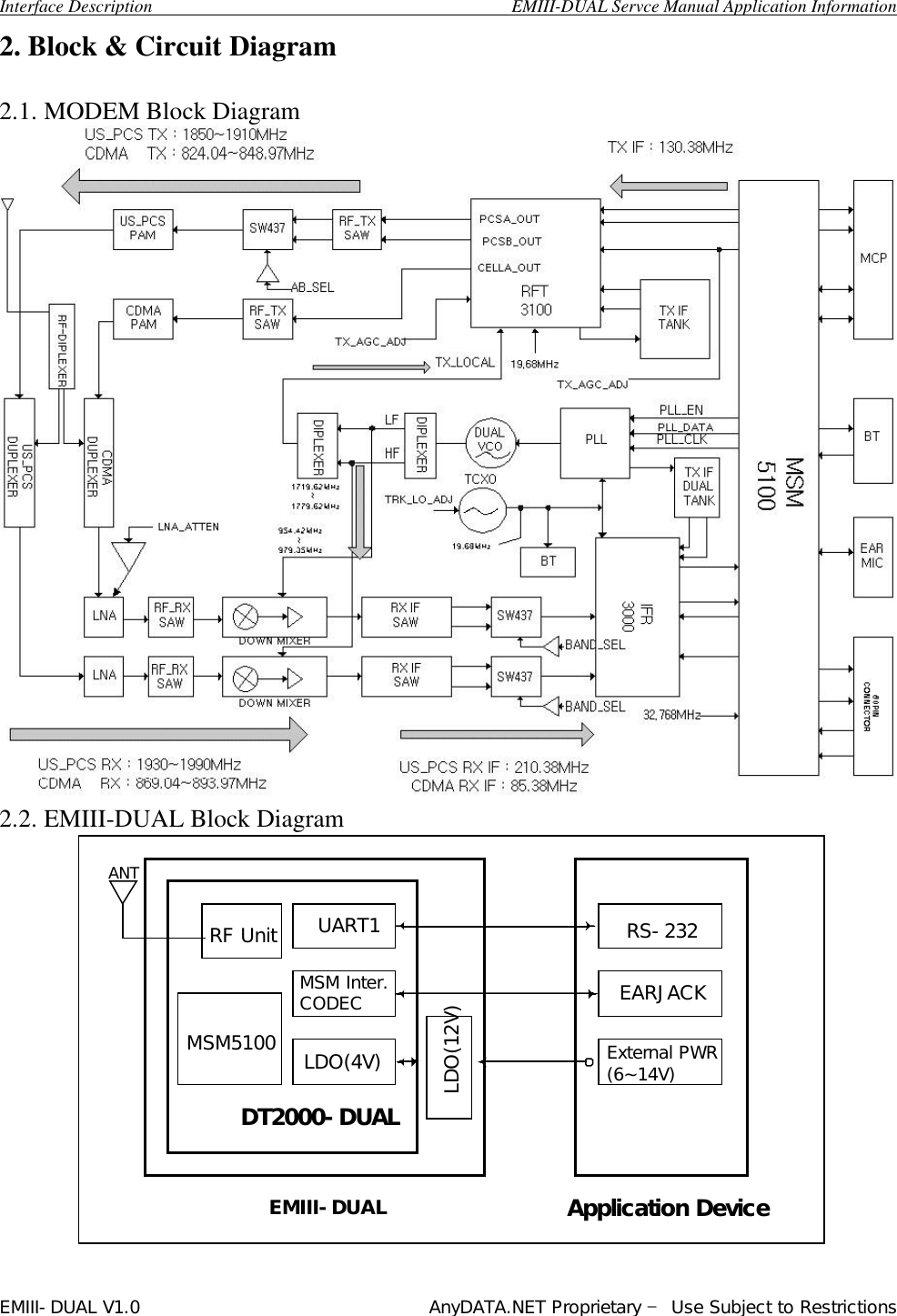
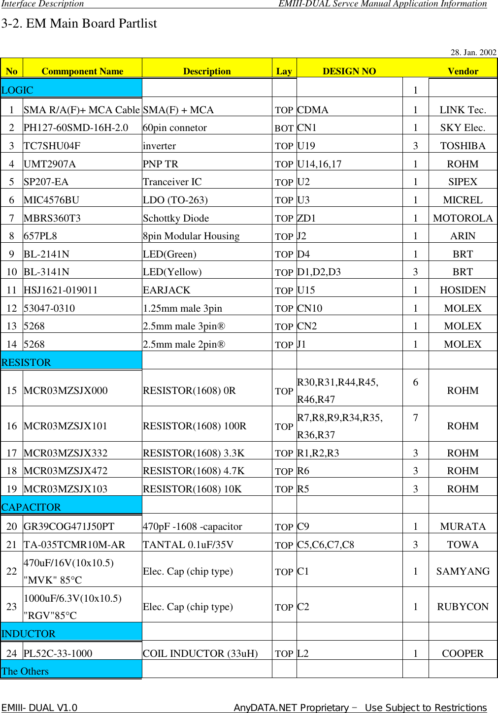
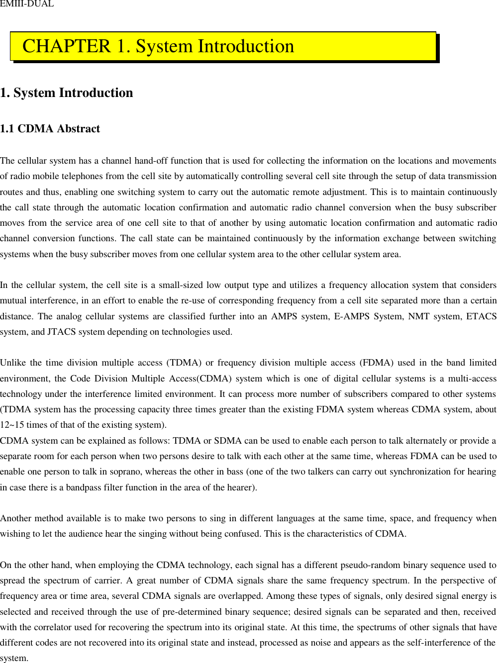
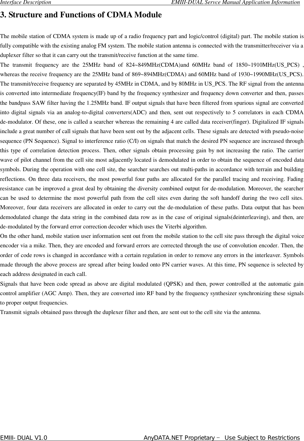
![Interface Description EMIII-DUAL Servce Manual Application Information EMIII-DUAL V1.0 AnyDATA.NET Proprietary – Use Subject to Restrictions 3.3 Circuit Description Ringer MCP (16M+4M) Receptacle Power Supply AUDIO Processor Earpiece Mic MSM5100 [Figure 3-1] Block Diagram of Digital/Voice Processing Part 3.3.1 MSM Part MSM5100, which is U401, is the core element of CDMA system terminal that includes ARM7TDMI microprocessor core. It is made up of a CPU, encoder, interleaver, deinterleaver, Viterbi decoder, MOD/DEM, and vocoder. MSM5100, when operated in the CDMA mode, utilizes CHIPX8 (9.8304MHz) as the reference clock that is received from IFR3000, and uses TCXO (19.68MHz) that is received from TCX201. CPU controls the terminal operation. Digital voice data that have been inputted are voice-encoded and variable-rated. Then, they are convolutionally encoded so that error detection and correction are possible. Coded symbols are interleaved in order to cope with multi-path fading. Each data channel is scrambled by the long code PN sequence of the user in order to ensure the confidentiality of calls. Moreover, binary quadrature codes are used based on Walsh functions in order to discern each channel. Data created thus are 4-phase modulated by one pair of Pilot PN code and they are used to create I and Q data. When received, I and Q data are demodulated into symbols by the demodulator and then, de-interleaved in reverse to the case of transmission. Then, the errors of data received from Viterbi decoder are detected and corrected. They are voice decoded at the vocoder in order to output digital voice data.](https://usermanual.wiki/AnyDATA/DT2000DUAL.Service-Manual/User-Guide-242042-Page-23.png)
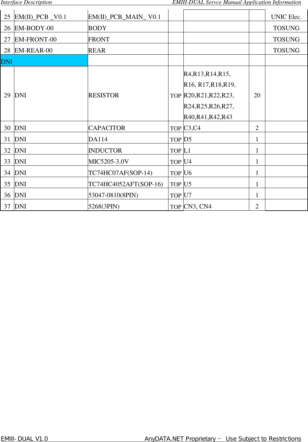
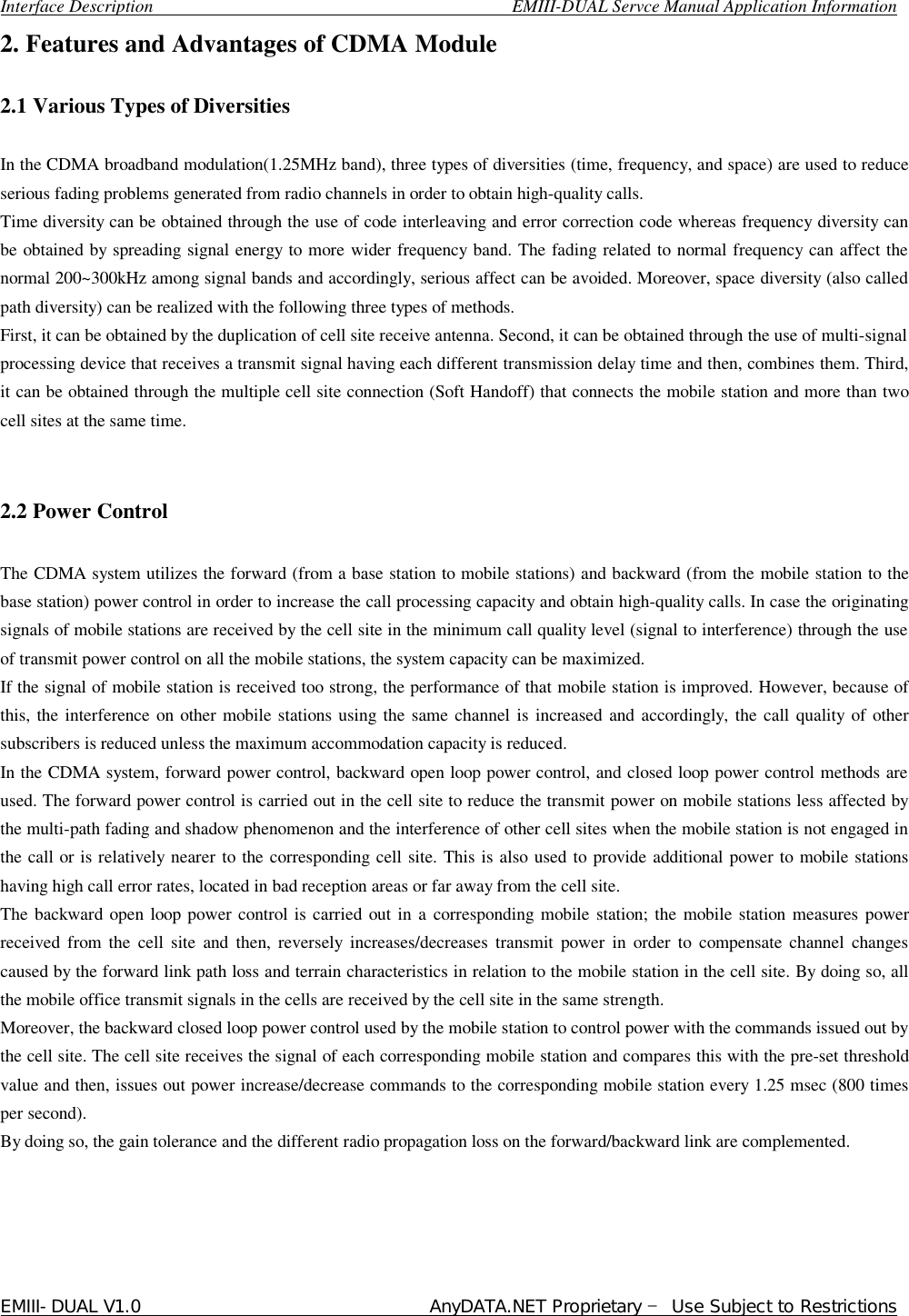
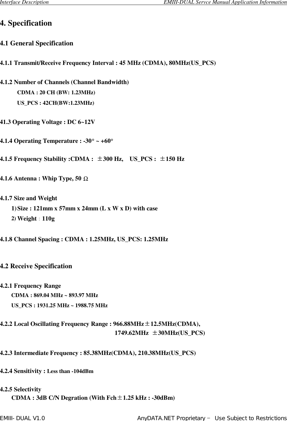
![Interface Description EMIII-DUAL Servce Manual Application Information EMIII-DUAL V1.0 AnyDATA.NET Proprietary – Use Subject to Restrictions 4. Level Translator Part 4.1 EMIII-DUAL supply power to Modem(4.0V). [Fig 4-1] The Block Diagram of Source (in brief) 4.2 UART Interface The Universal Asynchronous Receiver Transmitter (UART) communicates with serial data that conforms the RS-232 Interface protocol. The modem provides 3.0V CMOS level outputs and 3.0V CMOS switching input level. And all inputs have 5.0V tolerance but 3.0V or 3.3V CMOS logic compatible signals are highly recommended. All the control signals of the RS-232 signals are active low, but data signals of RXD, and TXD are active high. The UART has a 64byte transmit (TX) FIFO and a 64byte receive (RX) FIFO. The UART Features hardware handshaking, programmable data sizes, programmable stop bits, and odd, even, no parity. The UART operates at a 115.2kbps maximum bit rate. 4.2.1 UART Inter Pinouts NAME DESCRIPTION CHARACTERISTIC DP_DCD/ Data Carrier Detect Network connected from the modem DP_RI/ Ring Indicator Output to host indicating coming call DP_RTS/ Request to Send Ready for receive from host DP_TXD Transmit Data Output data from the modem DP_DTR/ Data Terminal Ready Host ready signal DP_RXD Receive Data Input data to the modem DP_CTS/ Clear to Send Modem output signal](https://usermanual.wiki/AnyDATA/DT2000DUAL.Service-Manual/User-Guide-242042-Page-25.png)
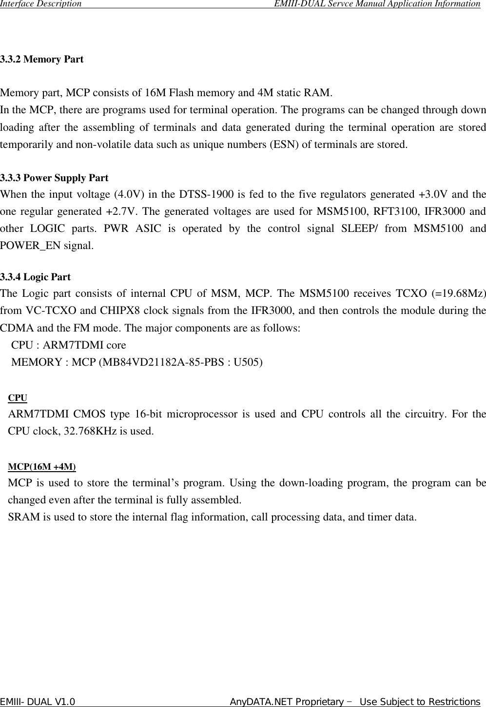
![Interface Description EMIII-DUAL Servce Manual Application Information EMIII-DUAL V1.0 AnyDATA.NET Proprietary – Use Subject to Restrictions NAME DESCRIPTION CHARACTERISTIC GND Signal Ground Signal ground 4.2.2 Signal level of RXD/TXD PC RS232 TX RX 01 03 DT2000 -DUAL Vout= 2.8V +3V +3V MSM_input MSM_output SIPEX207 +4VV EMIII-DUAL02 04 RS232 PHONE TX01 RX02 TX04 RX03 VMAX = 7.68V VMIN = -7.68V VMAX = 6.50V VMIN = -6.64V VMAX = 3.00V VMIN = 0V VMAX = 3.9V VMIN = 0V [Figure 4-2] Signal Level of RXD, TXD 4.3 The function of Real Audio Test( including Voice Test) NAME TYPE DESCRIPSION MIC+ I Microphone audio input MIC- IS Ear/microphone set detect EAR O Ear audio output GND_A Audio ground](https://usermanual.wiki/AnyDATA/DT2000DUAL.Service-Manual/User-Guide-242042-Page-26.png)