Arcadyan Technology WN7911A 2.4GHZ SDIO Sip Module User Manual WN7911A LF manual BVADT
Arcadyan Technology Corporation 2.4GHZ SDIO Sip Module WN7911A LF manual BVADT
User Manual.pdf

USER MANUAL
WN7911A-LF 1
USER MANUAL
WN7911A-LF
MPN F0ILF7911000J
(Hirose 1.5 mm Connector)
1x1 Single Band
802.11 b/g/n WiFi Module
V 1.2
.

USER MANUAL
WN7911A-LF 2
Introduction
1.1 Introduction
WN7911A-LF is a 1x1 single-band 2.4GHz IEEE 802.11 b/g/n WiFi module with
on-board PCB printed antenna. WN7911A-LF attains the data transmission speed up to
150 Mbps and provide SDIO physical interface to the board for WiFi. This WiFi
module is the low power consumption, high performance and the best WiFi solution
for consumer devices which need the compact size embedded WiFi module for
wireless connectivity like smart mobile phone, e-book, printer, tablet PC and so on.
1.2 Product Features
Small form factor: 25mm x 18mm x 2.4mm
High speed for wireless LAN connection, up to 150 Mbps for uplink and 150 Mbps for
downlink
Backward compatible to the existing IEEE 802.11b/g WLAN infrastructure
Low power consumption and excellent power management
Security features
WPA
TM
and WPA2
TM
(personal) support for powerful encryption and
authentication
AES and TKIP acceleration hardware for fast data encryption and 802.11i
compatibility
Cisco Compatible Extension (CCX, CCX 2.0, CCX 3.0, CCX 4.0) certified
SecureEasySetup
TM
for simple WiFi setup and configuration
Support WPS
QOS features
802.11e
802.11h
802.11i
802.11j
USER MANUAL
WN7911A-LF 3
2 Bill of Material
Item
QTY
Reference Part Description Vendor P/N Manufacturer
1
10
C3,C5,C7,C11,C13,
C16,C17,C19,C23,C25
0.1uF
C SMD CER 0.1uF 10% 16V X7R 0402 T0.5 HF MURATA
2
3
C4,C6,C8 10uF C SMD CER 10uF 20% 6.3V X5R 0603 T0.8mm HF CC0603MRX5R5BB106 YAGEO
3
7
C9,R19,R20,R21,R22,
R23,R26
DNI
4
8
C10,C12,C14,C18,C20,
C22,C24,C26
2.2uF
C SMD CER 2.2uF 10% 6.3V X5R 0603 T0.8mm LT/LF 0603X225K6R3CT WALSIN
5
1
R17 0 OHM RES SMD 0ohm 1/16W 0402 T0.35 HF WALSIN
6
1
C46 1.8pF C SMD HIGH-Q CER 1.8pF 0.25pF 50V NPO 0402 T0.5 HF WALSIN
7
1
C48 0.5pF C SMD HIGH-Q CER 0.5pF +-0.25
pF 50V NPO 0402 T0.5 HF
MURATA
8
1
C51 3.3nH IND SMD 3.3nH +-0.1nH 190 mA 0402 LT/LF MURATA
9
1
L1 600 OHM BEAD 100MHz 25% 1Kohm 100mA 0402 HF TAI-TECH
10
1
L2 INDUCTOR ?!IND SMD 3.3uH 20% 1200mA 2.5x2.0 HF MURATA
11
1
R1 10K RES SMD 10Kohm 5% 1/10W 0603 T0.45 HF WR06X103JTL WALSIN
12
1
J1 Connector
0.5 mm Pitch 1.5 mm Mating Height 14 Pin Plug
Board-to-Board Connector.
DF23C-14DP-0.5V HIROSE
13
1
U1 WS5700B-ZZ 802.11b/g/n 2.4GHz SDIO SiP Module Arcadyan
14
1
WN7911A-LF PCB footprint R0A3 PCB WN7911A-LF Carrier Board PCB ANT (4L) Arcadyan
USER MANUAL
WN7911A-LF 4
3 Pin Definition
Pin # Type
Description
1 P Ground
2 I/O SDIO Data Line 2
3 I/O SDIO Clock
4 P Ground
5 P Ground
6 I System Reset
7 I/O SDIO Data Line 0
8 I/O SDIO Command
9 P Ground
10 P Ground
11 I/O SDIO Data Line 1
12 I/O SDIO Data Line 3
13 P SDIO_VCC 3.3V
14 P SDIO_VCC 3.3V
USER MANUAL
WN7911A-LF 5
4 SiP Module
4.1 General Overview
Item Description
SiP Module Dimension 10mm x 10mm x 1.2mm
Chipset Broadcom BCM4319 1x1 Single Band (2.4GHz)
802.11n MAC/BB/RF on single chip with integrated
CMOS PA.
Module Interface SDIO (4-bit)
Module Pin Connection 48-pin LGA
4.2 SiP Module Architecture
4.2.1 WS5700B
USER MANUAL
WN7911A-LF 6
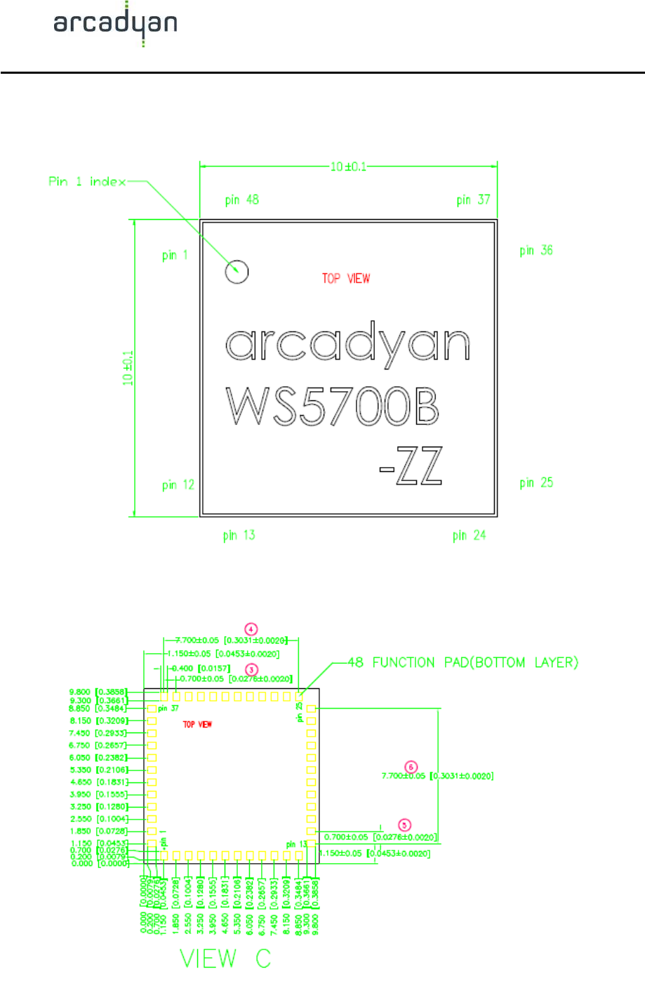
4.3 Outline Drawing
4.3.1 Top Side View
4.3.2 Bottom Side View
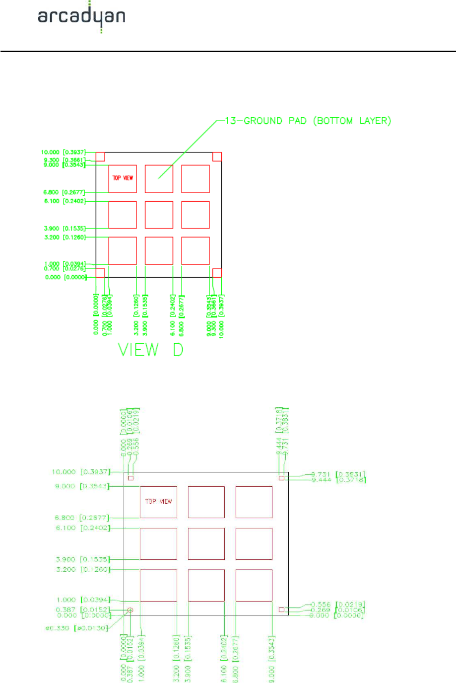
4.4 Dimension, Marking and Pin Layout
4.4.1 Side View
USER MANUAL
WN7911A-LF 7
4.4.2 Top Side View
4.4.3 Bottom Side Function Pad (Top View)
USER MANUAL
WN7911A-LF 8
4.4.4 Bottom Side Ground Pad (Top View)
4.4.5 Suggested Ground Pad Foot Print (Top View)

USER MANUAL
WN7911A-LF 9
4.5 Pin Description
Pin
# Terminal Name Pin
Type
I/O
Type
Description
1 BTCX_RF_ACTIVE Signal
I Indicates that the coexistent BT is active:
internal pull-down.
2 BTCX_STATUS Signal
I Indicates the coexistent BT priority status and
RX/TX direction.
3 USB_AVDD12 Power
I USB Phy core 1.2V supply
4 USB_AVDD25 Power
I USB Phy analog 2.5V supply
5 USB_AVDD33 Power
I USB Phy analog 3.3V supply
6 VDD_AFE Power
I 1.2V filtered supply for ADC; 1.2V filtered
supply for AFE AUX
7 GND Power
I Ground
8 USB20_DEV_DPLS Signal
I/O USB port data plus
9 USB20_DEV_DMNS
Signal
I/O USB port data minus
10 GND Power
I Ground
11 BTCX_FREQ Signal
I
Indicates that the coexistent BT is about to
transmit on a restricted channel: internal
pull-down.
12 GPIO_8 Signal
I/O General-purpose interface pins.
13 BTCX_TXCONF Signal
O Output permission for the coexistent BT to
transmit.
14 UART_TX Signal
O Serial Input for UART
15 UART_RX Signal
I Serial Output for UART
16 GND Power
I Ground
17 VIN_LDO Power
I Input supply pin for CLDO and LNLDO1
18 VDD_CORE_1.2V Power
O 1.2V output for core LDO, 200mA
19 VDD_RADIO_PLL_O
Power
O 1.2V output for low noise LNLDO1, 150mA

USER MANUAL
WN7911A-LF 10
20 VDD_3.3V Power
O Internal PALDO output or feedback of output
from external PNP
21 GPIO_0 Signal
I/O General-purpose interface pins.
22 VDD_2.5V Power
O 2.5V LDO2p5 output
23 GND Power
I Ground
24 VLX Power
O Core buck regulator: Output to inductor
25 VIN_3V_5V Power
I Battery supply input for PALDO;
Core buck regulator: Battery voltage input
26 GPIO_2 Signal
I/O General-purpose interface pins.
27 GND Power
I Ground
28 SDIO_CLK Signal
I/O SDIO clock
29 GPIO_3 Signal
I/O General-purpose interface pins.
30 SDIO_DATA_0 Signal
I/O SDIO data line 0
31 GPIO_1 Signal
I/O General-purpose interface pins.
32 SDIO_DATA_1 Signal
I/O SDIO data line 1
33 SDIO_DATA_2 Signal
I/O SDIO data line 2
34 GPIO_9 Signal
I/O General-purpose interface pins.
35 RESETn Signal
I
Low asserting global chip reset: digital input
pin.
Used by PMU to enable/disable power the
internal regulators.
36 SDIO_CMD Signal
I/O SDIO command line
37 SDIO_DATA_3 Signal
I/O SDIO data line 3
38 VDDIO Power
I
Digital I/O supply (1.8V to 3.3V)
VDDIO should be supplied externally;
SDIO I/O supply (1.8V to 3.3V)
39 GND Power
I Ground

USER MANUAL
WN7911A-LF 11
40 VDD_PLL Power
I 1.2V supply for PLL;
1.2V crystal oscillator filtered power supply
41 GND Power
I Ground
42 VDD_RADIO_PLL_I Power
I 1.2V supply for radio transmit and receive
sections
43 GND Power
I Ground
44 GND Power
I Ground
45 GND Power
I Ground
46 ANT Signal
I/O Antenna port
47 GND Power
I Ground
48 VDD_3.3V Power
I
RF I/O supply (2.6V to 3.3V);
3.3V OTP power supply (no lower than 3.0V);
3.3V for the internal power amplifiers
G1 GND Power
I Ground pad
G2 GND Power
I Ground pad
G3 GND Power
I Ground pad
G4 GND Power
I Ground pad
G5 GND Power
I Ground pad
G6 GND Power
I Ground pad
G7 GND Power
I Ground pad
G8 GND Power
I Ground pad
G9 GND Power
I Ground pad
G10
GND Power
I Ground pad
G11
GND Power
I Ground pad
G12
GND Power
I Ground pad
G13
GND Power
I Ground pad
USER MANUAL
WN7911A-LF 12
4.6 Bill of Materials
5 Software
5.1 Driver Support
Android v2.2 – v4.0
Linux v2.6.29 – v2.6.39
Windows CE (check for availability)

USER MANUAL
WN7911A-LF 13
6 Specifications
6.1 Frequency Band:
802.11n Radio: 2.4 GHz
802.11b/g Radio: 2.4 GHz
6.2 Transmit Power and Sensitivity:
TX Output Power:
11b 16 +/- 1 dBm
11g 14 +/- 1 dBm
11n 13 +/- 1 dBm
RX Sensitivity:
-86 dBm @ 11 Mbps
-72 dBm @ 54 Mbps
-68 dBm @ 64-QAM, 20 MHz channel spacing
6.3 Modulation
DBPSK @1 Mbps
DQPSK @2 Mbps
CCK @5.5/11 Mbps
BPSK @6/9 Mbps
QPSK @12/18 Mbps
16-QAM @24 Mbps
64-QAM @48/54 Mbps and above, up to 300 Mbps
6.4 Operation Voltage & Current Consumptions:
SDIO_VCC: 2.7V – 5.5V
VDD_IO: 1.8V or 3.3V (Operational: 1.62V – 3.63V)
TX: 263mA x 3.3V Max
RX: 81.58mA x 3.3V Max
Power Saving Mode: 1.25mA x 3.3V
Deep Sleep Mode: 130uA

USER MANUAL
WN7911A-LF 14
6.5 Module Dimension & Tolerance
18 +/- 0.1mm (W) X 25 +/- 0.1mm (L) X 2.4 +/- 0.1mm (H)
6.6 Temperature and Humidity
Operating Temperature: 0 ~ 40
o
C
Storage Temperature: -10 ~ 70
o
C
Humidity: 5 ~ 90% and must be non-condensing
6.7 Regulatory and Certification Compliance
FCC & CE Compliance
The drawings, specifications and the data contain herein are the exclusive property of Arcadyan
Technology Corp. issued in strict confidence and shall not, without the prior written permission of
Arcadyan Technology Corp., be reproduced, copied or used, in parts or as a whole, for any purpose
whatsoever, except the manufacture of articles for Arcadyan Technology Corp.
Arcadyan makes no warranties with respect to the correctness, accuracy or wholeness of this
specification. The information in this document is subject to change without notice. Arcadyan
reserves the right to make revisions to this document and the product described herein without
obligation to notify any person or entity of any such changes.

USER MANUAL
WN7911A-LF 15
Federal Communication Commission Interference Statement
This device complies with Part 15 of the FCC Rules. Operation is subject to the
following two conditions: (1) This device may not cause harmful interference, and (2)
this device must accept any interference received, including interference that may
cause undesired operation.
This equipment has been tested and found to comply with the limits for a Class B
digital device, pursuant to Part 15 of the FCC Rules. These limits are designed to
provide reasonable protection against harmful interference in a residential installation.
This equipment generates, uses and can radiate radio frequency energy and, if not
installed and used in accordance with the instructions, may cause harmful interference
to radio communications. However, there is no guarantee that interference will not
occur in a particular installation. If this equipment does cause harmful interference
to radio or television reception, which can be determined by turning the equipment off
and on, the user is encouraged to try to correct the interference by one of the following
measures:
- Reorient or relocate the receiving antenna.
- Increase the separation between the equipment and receiver.
- Connect the equipment into an outlet on a circuit different from that
to which the receiver is connected.
- Consult the dealer or an experienced radio/TV technician for help.
FCC Caution: Any changes or modifications not expressly approved by the party
responsible for compliance could void the user's authority to operate this equipment.
This transmitter must not be co-located or operating in conjunction with any other
antenna or transmitter.
Radiation Exposure Statement:
This equipment complies with FCC radiation exposure limits set forth for an
uncontrolled environment. This equipment should be installed and operated with
minimum distance 20cm between the radiator & your body.

USER MANUAL
WN7911A-LF 16
This device is intended only for OEM integrators under the following conditions:
1) The antenna must be installed such that 20 cm is maintained between the antenna
and users, and
2) The transmitter module may not be co-located with any other transmitter or antenna.
As long as 2 conditions above are met, further transmitter test will not be required.
However, the OEM integrator is still responsible for testing their end-product for any
additional compliance requirements required with this module installed
IMPORTANT NOTE: In the event that these conditions can not be met (for example
certain laptop configurations or co-location with another transmitter), then the FCC
authorization is no longer considered valid and the FCC ID can not be used on the final
product. In these circumstances, the OEM integrator will be responsible for
re-evaluating the end product (including the transmitter) and obtaining a separate FCC
authorization.
End Product Labeling
This transmitter module is authorized only for use in device where the antenna may be
installed such that 20 cm may be maintained between the antenna and users. The final
end product must be labeled in a visible area with the following: “Contains FCC ID:
RAXWN7911A”. The grantee's FCC ID can be used only when all FCC compliance
requirements are met.
Manual Information To the End User
The OEM integrator has to be aware not to provide information to the end user regarding
how to install or remove this RF module in the user’s manual of the end product which
integrates this module.
The end user manual shall include all required regulatory information/warning as show
in this manual.