Asus H61M Cs Users Manual ManualsLib Makes It Easy To Find Manuals Online!
2014-12-12
: Asus Asus-H61M-Cs-Users-Manual-118936 asus-h61m-cs-users-manual-118936 asus pdf
Open the PDF directly: View PDF ![]() .
.
Page Count: 242 [warning: Documents this large are best viewed by clicking the View PDF Link!]

Intel® 820 Chipset
Design Guide
July 2000
Order Number: 290631-004

Intel® 820 Chipset Design Guide
Information in this document is provided in connection with Intel products. No license, express or implied, by estoppel or otherwise, to any intellectual
property rights is granted by this document. Except as provided in Intel's Terms and Conditions of Sale for such products, Intel assumes no liability
whatsoever, and Intel disclaims any express or implied warranty, relating to sale and/or use of Intel products including liability or warranties relating to
fitness for a particular purpose, merchantability, or infringement of any patent, copyright or other intellectual property right. Intel products are not
intended for use in medical, life saving, or life sustaining applications.
Intel may make changes to specifications and product descriptions at any time, without notice.
Contact your local Intel sales office or your distributor to obtain the latest specifications and before placing your product order.
The Intel® 820 chipset may contain design defects or errors known as errata which may cause the product to deviate from published specifications.
Current characterized errata are available on request.
I2C is a two-wire communications bus/protocol developed by Philips. SMBus is a subset of the I2C bus/protocol and was developed by Intel.
Implementations of the I2C bus/protocol or the SMBus bus/protocol may require licenses from various entities, including Philips Electronics N.V. and
North American Philips Corporation.
Alert on LAN and Wake on LAN are results of the IBM/Intel Advanced Manageability Alliance and are trademarks of IBM Corporation.
Copies of documents which have an ordering number and are referenced in this document, or other Intel literature may be obtained by:
calling 1-800-548-4725 or
by visiting Intel's website at http://www.intel.com.
Copyright © Intel Corporation, 2000
*Third-party brands and names are the property of their respective owners.

Intel® 820 Chipset Design Guide iii
Contents
1 Introduction ................................................................................................................1-1
1.1 About This Design Guide..............................................................................1-1
1.2 References....................................................................................................1-2
1.3 System Overview..........................................................................................1-2
1.3.1 Chipset Components .......................................................................1-3
1.3.2 Bandwidth Summary........................................................................1-4
1.3.3 System Configuration.......................................................................1-5
1.4 Platform Initiatives.........................................................................................1-8
1.4.1 Direct Rambus*................................................................................1-8
1.4.2 Streaming SIMD Extensions ............................................................1-8
1.4.3 AGP 2.0 ...........................................................................................1-8
1.4.4 Hub Interface ...................................................................................1-8
1.4.5 Manageability...................................................................................1-9
1.4.6 AC’97 .............................................................................................1-10
1.4.7 Low Pin Count (LPC) Interface ......................................................1-11
2 Layout/Routing Guidelines.........................................................................................2-1
2.1 General Recommendations ..........................................................................2-1
2.2 Component Quadrant Layout........................................................................2-1
2.3 Intel® 820 Chipset Component Placement ...................................................2-3
2.4 Core Chipset Routing Recommendations.....................................................2-4
2.5 Source Synchronous Strobing ......................................................................2-5
2.6 Direct Rambus* Interface..............................................................................2-7
2.6.1 Stackup............................................................................................2-8
2.6.2 Direct Rambus* Layout Guidelines..................................................2-8
2.6.3 Direct Rambus* Reference Voltage...............................................2-25
2.6.4 High-speed CMOS Routing ...........................................................2-25
2.6.5 Direct Rambus* Clock Routing ......................................................2-28
2.6.6 Direct Rambus* Design Checklist ..................................................2-28
2.7 AGP 2.0 ......................................................................................................2-31
2.7.1 AGP Interface Signal Groups.........................................................2-32
2.7.2 1X Timing Domain Routing Guidelines..........................................2-33
2.7.3 2X/4X Timing Domain Routing Guidelines.....................................2-33
2.7.4 AGP 2.0 Routing Summary............................................................2-35
2.7.5 AGP Clock Routing ........................................................................2-36
2.7.6 General AGP Routing Guidelines ..................................................2-36
2.7.7 VDDQ Generation and TYPEDET# ...............................................2-37
2.7.8 VREF Generation for AGP 2.0 (2X and 4X) ....................................2-39
2.7.9 Compensation................................................................................2-41
2.7.10 AGP Pull-ups .................................................................................2-41
2.7.11 Motherboard / Add-in Card Interoperability....................................2-42
2.8 Hub Interface ..............................................................................................2-43
2.8.1 Data Signals...................................................................................2-44
2.8.2 Strobe Signals................................................................................2-44
2.8.3 HREF Generation/Distribution .......................................................2-44
2.8.4 Compensation................................................................................2-45

iv Intel® 820 Chipset Design Guide
2.9 System Bus Design ....................................................................................2-46
2.9.1 100/133 MHz System Bus .............................................................2-46
2.9.2 System Bus Ground Plane Reference...........................................2-47
2.10 S.E.C.C. 2 Grounding Retention Mechanism (GRM) .................................2-47
2.11 Processor CMOS Pullup Values.................................................................2-49
2.12 Additional Host Bus Guidelines ..................................................................2-52
2.13 Ultra ATA/66 ...............................................................................................2-56
2.13.1 Ultra ATA/66 Detection..................................................................2-56
2.13.2 Ultra ATA/66 Cable Detection........................................................2-57
2.13.3 Ultra ATA/66 Pullup/Pulldown Requirements ................................2-60
2.14 AC’97..........................................................................................................2-61
2.14.1 AC’97 Signal Quality Requirements...............................................2-63
2.14.2 AC’97 Motherboard Implementation..............................................2-63
2.15 USB ............................................................................................................2-65
2.16 ISA (82380AB)............................................................................................2-66
2.16.1 ICH GPIO connected to 82380AB .................................................2-66
2.16.2 Sub Class Code.............................................................................2-66
2.17 IOAPIC Design Recommendation ..............................................................2-66
2.18 SMBus/Alert Bus.........................................................................................2-67
2.19 PCI..............................................................................................................2-67
2.20 RTC ............................................................................................................2-67
2.20.1 RTC Crystal ...................................................................................2-68
2.20.2 External Capacitors .......................................................................2-68
2.20.3 RTC Layout Considerations...........................................................2-69
2.20.4 RTC External Battery Connection..................................................2-69
2.20.5 RTC External RTCRST Circuit.......................................................2-70
2.20.6 RTC Routing Guidelines ................................................................2-70
2.20.7 VBIAS DC Voltage and Noise Measurements...............................2-71
3 Advanced System Bus Design ..................................................................................3-1
3.1 Terminology and Definitions .........................................................................3-1
3.2 AGTL+ Design Guidelines ............................................................................3-4
3.2.1 Initial Timing Analysis ......................................................................3-5
3.2.2 Determine General Topology, Layout, and Routing Desired ...........3-8
3.2.3 Pre-Layout Simulation .....................................................................3-8
3.2.4 Place and Route Board..................................................................3-10
3.2.5 Post-Layout Simulation..................................................................3-13
3.2.6 Validation .......................................................................................3-14
3.3 Theory.........................................................................................................3-15
3.3.1 AGTL+ ...........................................................................................3-15
3.3.2 Timing Requirements.....................................................................3-16
3.3.3 Cross-talk Theory ..........................................................................3-16
3.4 More Details and Insight .............................................................................3-19
3.4.1 Textbook Timing Equations ...........................................................3-19
3.4.2 Effective Impedance and Tolerance/Variation ...............................3-20
3.4.3 Power/Reference Planes, PCB Stackup, and High
Frequency Decoupling...................................................................3-20
3.4.4 Clock Routing ................................................................................3-23

Intel® 820 Chipset Design Guide v
3.5 Definitions of Flight Time Measurements/Corrections and Signal Quality ..3-24
3.5.1 VREF Guardband............................................................................3-24
3.5.2 Ringback Levels.............................................................................3-24
3.5.3 Overdrive Region...........................................................................3-24
3.5.4 Flight Time Definition and Measurement .......................................3-25
3.6 Conclusion ..................................................................................................3-26
4 Clocking .....................................................................................................................4-1
4.1 Clock Generation ..........................................................................................4-1
4.2 Component Placement and Interconnection Layout Requirements..............4-6
4.2.1 14.318 MHz Crystal to CK133 .........................................................4-6
4.2.2 CK133 to DRCG ..............................................................................4-6
4.2.3 MCH to DRCG .................................................................................4-7
4.2.4 DRCG to RDRAM Channel..............................................................4-8
4.2.5 Trace Length....................................................................................4-8
4.3 DRCG Impedance Matching Circuit............................................................4-10
4.3.1 DRCG Layout Example..................................................................4-11
4.4 AGP Clock Routing Guidelines...................................................................4-11
4.5 Series Termination Resistors for CK133 Clock Outputs.............................4-11
4.6 Unused Outputs..........................................................................................4-12
4.7 Decoupling Recommendation for CK133 and DRCG .................................4-12
4.8 DRCG Frequency Selection and the DRCG+.............................................4-12
4.8.1 DRCG Frequency Selection Table and Jitter Specification ...........4-12
4.8.2 DRCG+ Frequency Selection Schematic.......................................4-13
5 System Manufacturing ...............................................................................................5-1
5.1 In Circuit LPC Flash BIOS Programming......................................................5-1
5.2 LPC Flash BIOS Vpp Design Guidelines......................................................5-1
5.3 Stackup Requirement ...................................................................................5-1
5.3.1 Overview ..........................................................................................5-1
5.3.2 PCB Materials..................................................................................5-2
5.3.3 Design Process................................................................................5-2
5.3.4 Test Coupon Design Guidelines ......................................................5-3
5.3.5 Recommended Stackup...................................................................5-3
5.3.6 Inner Layer Routing .........................................................................5-3
5.3.7 Impedance Calculation Tools...........................................................5-4
5.3.8 Testing Board Impedance................................................................5-4
5.3.9 Board Impedance/Stackup Summary ..............................................5-5
6 System Design Considerations..................................................................................6-1
6.1 Power Delivery..............................................................................................6-1
6.1.1 Terminology and Definitions ............................................................6-1
6.1.2 Intel® 820 Chipset Customer Reference Board Power Delivery......6-2
6.1.3 64/72Mbit RDRAM Excessive Power Consumption ........................6-5
6.2 Power Plane Splits........................................................................................6-7
6.3 Thermal Design Power .................................................................................6-7
6.4 Glue Chip 3 (Intel® 820 Chipset Glue Chip) .................................................6-8
A Reference Design Schematics: Uni-Processor......................................................... A-1
A.1 Reference Design Feature Set .................................................................... A-1
B Reference Design Schematics: Dual-Processor....................................................... B-1
B.1 Reference Design Feature Set .................................................................... B-1

vi Intel® 820 Chipset Design Guide
Figures
1-1 Intel® 820 Chipset Platform Performance Desktop Block Diagram ..............1-5
1-2 Intel® 820 Chipset Platform Performance Desktop Block Diagram
(with ISA Bridge)...........................................................................................1-6
1-3 Intel® 820 Chipset Platform Dual-Processor Performance Desktop
Block Diagram ..............................................................................................1-7
1-4 AC’97 Connections .....................................................................................1-11
2-1 MCH 324-uBGA Quadrant Layout (Top View)..............................................2-2
2-2 ICH 241-uBGA Quadrant Layout (Top View)................................................2-2
2-3 Sample ATX MCH/ICH Component Placement............................................2-3
2-4 Primary Side MCH Core Routing Example (ATX) ........................................2-4
2-5 Secondary Side MCH Core Routing Example (ATX)....................................2-5
2-6 Data Strobing Example.................................................................................2-6
2-7 Effect of Crosstalk on Strobe Signal .............................................................2-6
2-8 RIMM Diagram..............................................................................................2-7
2-9 RSL Routing Dimensions..............................................................................2-9
2-10 RSL Routing Diagram...................................................................................2-9
2-11 Primary Side RSL Breakout Example.........................................................2-10
2-12 Secondary Side RSL Breakout Example....................................................2-11
2-13 Direct RDRAM Termination ........................................................................2-11
2-14 Direct Rambus* Termination Example........................................................2-12
2-15 Incorrect Direct Rambus* Ground Plane Referencing................................2-13
2-16 Direct Rambus Ground Plane Reference ...................................................2-13
2-17 Connector Compensation Example............................................................2-16
2-18 Section A1, Top Layer.................................................................................2-17
2-19 Section A1, Bottom Layer ...........................................................................2-18
2-20 Section B1, Top Layer.................................................................................2-19
2-21 Section B1, Bottom Layer ...........................................................................2-20
2-22 RSL Signal Layer Alternation .....................................................................2-21
2-23 RDRAM Trace Length Matching Example..................................................2-22
2-24 "Dummy" Via vs. Real "Via"........................................................................2-23
2-25 RAMRef Generation Example Circuit ........................................................2-25
2-26 High-Speed CMOS Termination .................................................................2-26
2-27 SIO Routing Example .................................................................................2-26
2-28 RDRAM CMOS Shunt Transistor ..............................................................2-27
2-29 AGP 2X/4X Routing Example for Interfaces < 6”........................................2-34
2-30 Top Signal Layer.........................................................................................2-37
2-31 AGP VDDQ Generation Example Circuit....................................................2-39
2-32 AGP 2.0 VREF Generation & Distribution ..................................................2-40
2-33 Hub Interface Signal Routing Example.......................................................2-43
2-34 Single Hub Interface Reference Divider Circuit ..........................................2-44
2-35 Locally generated Hub Interface Reference Dividers .................................2-45
2-36 Intel® Pentium® III Processor Dual Processor Configuration .....................2-46
2-37 Intel® Pentium® III Processor Uni-Processor Configuration .......................2-46
2-38 Ground Plane Reference (Four Layer Motherboard)..................................2-47
2-39 Hole Locations and Keepout Zones For Support Components ..................2-48
2-40 Grounding Pad Dimensions for the SECC2 GRM ......................................2-48
2-41 TCK/TMS Implementation Example for DP Designs ..................................2-52
2-42 Single Processor BREQ Strapping Requirements......................................2-52
2-43 Dual-Processor BREQ Strapping Requirements ........................................2-53

Intel® 820 Chipset Design Guide vii
2-44 BREQ0# Circuitry for DP Systems..............................................................2-53
2-45 HA7# Strapping Option Example Circuit (For Debug Purposes Only)........2-54
2-46 Host-Side IDE Cable Detection...................................................................2-57
2-47 Drive-Side IDE Cable Detection..................................................................2-58
2-48 Layout for Host- or Drive-Side IDE Cable Detection...................................2-59
2-49 Ultra ATA/66 Cable.....................................................................................2-59
2-50 Resistor Requirements for Primary IDE Connector ....................................2-60
2-51 Resistor Requirements for Secondary IDE Connector ...............................2-61
2-52 Tee Topology AC'97 Trace Length Requirements......................................2-62
2-53 Daisy-Chain Topology AC'97 Trace Length Requirements ........................2-62
2-54 USB Data Signals .......................................................................................2-65
2-55 PCI Bus Layout Example............................................................................2-67
2-56 External Circuitry for the ICH RTC..............................................................2-68
2-57 Diode Circuit Connecting RTC External Battery .........................................2-69
2-58 RTCRST External Circuit for the ICH RTC .................................................2-70
3-1 PICD[1,0] Uni-Processor Topology.............................................................3-12
3-2 PICD[1,0] Dual-Processor Topology...........................................................3-12
3-3 Test Load vs. Actual System Load .............................................................3-14
3-4 Aggressor and Victim Networks..................................................................3-17
3-5 Transmission Line Geometry: (A) Microstrip (B) Stripline...........................3-17
3-6 One Signal Layer and One Reference Plane..............................................3-21
3-7 Layer Switch with One Reference Plane ....................................................3-21
3-8 Layer Switch with Multiple Reference Planes (same type).........................3-21
3-9 Layer Switch with Multiple Reference Planes .............................................3-22
3-10 One Layer with Multiple Reference Planes.................................................3-22
3-11 Overdrive Region and VREF Guardband.....................................................3-25
3-12 Rising Edge Flight Time Measurement.......................................................3-25
4-1 Intel® 820 Chipset Platform Clock Distribution .............................................4-2
4-2 Intel® 820 Chipset Clock Routing Guidelines ...............................................4-4
4-3 CK133 to DRCG Routing Diagram ...............................................................4-6
4-4 MCH to DRCG Routing Diagram ..................................................................4-7
4-5 Direct Rambus* Clock Routing Dimensions..................................................4-7
4-6 Differential Clock Routing Diagram (Section ‘A’, ‘C’, & ‘D’)...........................4-9
4-7 Non-Differential Clock Routing Diagram (Section ‘B’)...................................4-9
4-8 Termination for Direct Rambus* Clocking Signals CFM/CFM# ....................4-9
4-9 DRCG Impedance Matching Network.........................................................4-10
4-10 DRCG Layout Example...............................................................................4-11
4-11 DRCG+ Frequency Selection .....................................................................4-13
5-1 28Ω Trace Geometry ....................................................................................5-2
5-2 Microstrip and Stripline Cross-section for 28 Ω Trace ..................................5-4
5-3 7 mil Stackup (Not Routable)........................................................................5-5
5-4 4.5 mil Stackup .............................................................................................5-5
6-1 Intel® 820 Chipset Power Delivery Example.................................................6-2
6-2 1.8V and 2.5V Power Sequencing (Schottky Diode) ....................................6-4
6-3 Use a GPO to Reduce DRCG Frequency.....................................................6-6
6-4 Power Plane Split Example...........................................................................6-7

viii Intel® 820 Chipset Design Guide
Tables
1-1 Intel® 820 Chipset Platform Bandwidth Summary ........................................1-4
2-1 AGP 2X Data/Strobe Association .................................................................2-6
2-2 Placement Guidelines for Motherboard Routing Lengths .............................2-9
2-3 Copper Tab Area Calculation .....................................................................2-15
2-4 RSL Routing Layer Requirements ..............................................................2-21
2-5 Line Matching and Via Compensation Example .........................................2-24
2-6 Signal List ...................................................................................................2-28
2-7 AGP 2.0 Data/Strobe Associations.............................................................2-33
2-8 AGP 2.0 Routing Summary ........................................................................2-35
2-9 TYPDET#/VDDQ Relationship ...................................................................2-38
2-10 Connector/Add-in Card Interoperability ......................................................2-42
2-11 Voltage/Data Rate Interoperability..............................................................2-42
2-12 Segment Descriptions and Lengths for Figure 2-36 ...................................2-46
2-13 Processor and 82820 MCH Connection Checklist......................................2-49
2-14 Bus Request Connection Scheme for DP Intel® 820 Chipset Designs.......2-52
2-15 ICH Codec Options.....................................................................................2-61
2-16 AC'97 SDIN Pulldown Resistors.................................................................2-63
3-1 AGTL+ Parameters for Example Calculations..............................................3-6
3-2 Example TFLT_MAX Calculations for 133 MHz Bus .......................................3-7
3-3 Example TFLT_MIN Calculations (Frequency Independent)...........................3-8
3-4 Trace Width Space Guidelines ...................................................................3-11
3-5 Host Clock Routing .....................................................................................3-12
4-1 Intel® 820 Chipset Platform System Clocks..................................................4-1
4-2 Intel® 820 Chipset Platform Clock Skews.....................................................4-3
4-3 Intel® 820 Chipset Platform System Clock Cross-Reference .......................4-5
4-4 Placement Guidelines for Motherboard Routing Lengths .............................4-8
4-5 External DRCG Component Values ...........................................................4-10
4-6 Unused Output Termination........................................................................4-12
4-7 DRCG Ratio................................................................................................4-12
5-1 28Ω Stackup Examples ................................................................................5-3
5-2 3D Field Solver vs ZCALC............................................................................5-4
6-1 Intel® 820 Chipset Component Thermal Design Power................................6-7
6-2 Glue Chip 3 Vendors ....................................................................................6-8

Intel® 820 Chipset Design Guide ix
Revision History
Revision Description Date
-001 Initial Release. November 1999
-002
• Added dual-processor schematics (Appendix B).
• Uni-processor schematics have been updated (Appendix A). See the
schematic revision history page at the end of Appendix A for details.
- The following update is not in the schematic revision history.
Cap C249 (schematic page 9) has been changed from 0.022 uF to
0.047 uF.
December 1999
-003
• Updated the text descriptions in the two paragraphs in Section 4.2.3,
“MCH to DRCG”.
• Updated the first paragraph in Section 2.6.2.5, “RSL Signal Layer
Alternation“.
January 2000
-004 • Minor edits for clarity July 2000

xIntel® 820 Chipset Design Guide
This page is intentionally left blank.

1
Introduction
This page is intentionally left blank.

Intel®820 Chipset Design Guide 1-1
Introduction
Introduction 1
The Intel® 820 Chipset Design Guide provides design recommendations for systems using the
Intel® 820 chipset. This includes motherboard layout and routing guidelines, system design issues
and requirements, debug recommendations, and board schematics. The design recommendations
should be used during system design. The guidelines have been developed to ensure maximum
flexibility for board designers while reducing the risk of board-related issues.
The Intel board schematics in Appendix A (uni-processor) and Appendix B (dual-processor) can be
used as references for board designers. A feature list is provided at the beginning of each appendix.
Although these schematics cover specific designs, the core schematics for each chipset component
remains the same for most Intel® 820 chipset platforms. The appendices provides a set of reference
schematics for each chipset component, in addition to common motherboard options. Additional
flexibility is possible through other permutations of these options and components.
1.1 About This Design Guide
This design guide is intended for hardware designers who are experienced with PC architectures
and board design. The design guide assumes that the designer has a working knowledge of the
vocabulary and practices of PC hardware design.
•This chapter introduces the designer to the purpose and organization of this design guide, and
provides a list of references of related documents. This chapter also provides an overview of
the Intel® 820 chipset.
•Chapter 2, "Layout/Routing Guidelines"—This chapter provides a detailed set of motherboard
layout and routing guidelines for designing an Intel® 820 chipset based platform. The
motherboard functional units are covered (e.g., chipset component placement, system bus
routing, system memory layout, display cache interface, hub interface, IDE, AC’97, USB,
interrupts, SMBUS, PCD, LPC/FWH Flash BIOS, and RTC).
•Chapter 3, "Advanced System Bus Design"— AGTL+ guidelines and theory of operation are
discussed. This chapter also provides more detail about the methodologies used to develop the
guidelines.
•Chapter 4, "Clocking"— This chapter provides motherboard clocking guidelines (e.g., clock
architecture, routing, capacitor sites, clock power decoupling, and clock skew).
•Chapter 5, "System Manufacturing"— This chapter includes board stackup requirements.
•Chapter 6, "System Design Considerations"— This chapter includes guidelines regarding
power delivery, decoupling, thermal, and power sequencing.
•Appendix A, "Reference Board Schematics: Uni-Processor "— This appendix provides a set
of schematics for Uni-processor designs. A feature list for the board design is also provided.
•Appendix B, "Reference Board Schematics: Dual-Processor "— This appendix provides a set
of schematics for dual-processor designs. A feature list for the board design is also provided.

Introduction
1-2 Intel®820 Chipset Design Guide
1.2 References
•Intel® 820 Chipset: Intel® 82820 Memory Controller Hub (MCH) Datasheet
(Order Number: 290630)
•Intel® 82801AA (ICH) and Intel® 82801AB (ICH0) I/O Controller Hub Datasheet
(Order Number: 290655)
•Intel® 82802AB/82802AC FirmWare Hub (FWH) Datasheet (Order Number: 290658)
•Pentium® II Processor AGTL+ Guidelines (Order Number: 243330)
•Pentium® II Processor Power Distribution Guideline (Order Number: 243332)
•Pentium® II Processor Developer's Manual (Order Number: 243341)
•Pentium® III Processor Specification Update (latest off of website)
•AP 907 Pentium III processor Power Distribution Guidelines (Order Number 245085)
•AP-585 Pentium II Processor AGTL+ Guidelines (Order Number: 243330)
•AP-587 Pentium II Processor Power Distribution Guidelines (Order Number: 243332)
•CK97 Clock Synthesizer Design Guidelines (Order Number 243867)
•PCI Local Bus Specification, Revision 2.2
•Universal Serial Bus Specification, Revision 1.0
•VRM 8.4 DC-DC Converter Design Guidelines (when available)
1.3 System Overview
The Intel® 820 chipset is the third generation desktop chipset designed for Intel’s SC242
architecture and the first chipset to support the 4X capability of the AGP 2.0 Interface Specification
and 400 MHz Direct RDRAM. The 400 MHz, 16 bit, double clocked Direct RDRAM interface
provides 1.6 GB/s access to main memory. A new chipset component interconnect, the hub
interface, is designed into the Intel® 820 chipset to provide more efficient communication between
chipset components.
Support of AGP 4X, 400 MHz Direct RDRAM and the hub interface provides a balanced system
architecture for the Pentium III processor, minimizing bottlenecks and increasing system
performance. By increasing memory bandwidth to 1.6 GB/s through the use of 400 MHz Direct
RDRAM and increasing graphics bandwidth to 1 GB/s through the use of AGP 4X, the Intel® 820
chipset delivers the data throughput necessary to take advantage of the high performance provided
by the powerful Pentium III processor.
In addition, the Intel® 820 chipset architecture enables a new security and manageability
infrastructure through the Firmware Hub component.
The ACPI compliant Intel® 820 chipset platform can support the Full-on, Stop Grant, Suspend to
RAM, Suspend to Disk, and Soft-off power management states. Through the use of an appropriate
LAN device, Intel® 820 chipset also supports Wake on LAN* for remote administration and
troubleshooting.
The Intel® 820 chipset architecture removes the requirement for the ISA expansion bus that was
traditionally integrated into the I/O subsystem of Intel chipsets. This removes many of the conflicts
experienced when installing hardware and drivers into legacy ISA systems. The elimination of ISA
provides true plug-and-play for the Intel® 820 chipset platform. Traditionally, the ISA interface
was used for audio and modem devices. The addition of AC’97 allows the OEM to use software

Intel®820 Chipset Design Guide 1-3
Introduction
configurable AC’97 audio and modem coder/decoders (codecs) instead of the traditional ISA
devices. The ISA bus can be implemented through the use of the optional 82380AB PCI-ISA
bridge.
The Intel® 820 chipset contains two core components: the Memory Controller Hub (MCH) and the
I/O Controller Hub (ICH). The MCH integrates the 133 MHz processor system bus controller,
AGP 2.0 controller, 400 MHz Direct RDRAM controller and a high-speed hub interface for
communication with the ICH. The ICH integrates an UltraATA/66 controller, USB host controller,
LPC interface controller, FWH Flash BIOS interface controller, PCI interface controller, AC’97
digital controller and a hub interface for communication with the MCH. The Intel® 820 chipset
provides the data buffering and interface arbitration required to ensure that system interfaces
operate efficiently and provide the system bandwidth necessary to obtain peak performance with
the Pentium III processor.
1.3.1 Chipset Components
This section provides an overview of the 82820 Memory Controller Hub (MCH) and the 82801AA
I/O Controller Hub (ICH). Additional functionality can be provided using the 82380AB PCI-ISA
bridge.
Memory Controller Hub (MCH)
The MCH provides the interconnect between the Direct RDRAM and the system logic. It integrates
the following functions:
•Support for single or dual SC242 processors with 100 MHz or 133 MHz System Bus
•256 MHz, 300 MHz, 356 MHz or 400 MHz Direct RDRAM interface supporting 1 GB of
Direct RDRAM
•4X, 1.5V AGP interface (3.3V 1X, 2X and 1.5V 1X, 2X devices also supported)
•Downstream hub interface for access to the ICH
In addition, the MCH provides arbitration, buffering and coherency management for each of these
interfaces. Refer to Chapter 2, “Layout/Routing Guidelines” for more information regarding these
interfaces.

Introduction
1-4 Intel®820 Chipset Design Guide
I/O Controller Hub (ICH)
The I/O Controller Hub provides the I/O subsystem with access to the rest of the system.
Additionally, it integrates many I/O functions. The ICH integrates the following functions:
•Upstream hub interface for access to the MCH
•2 channel Ultra ATA/66 Bus Master IDE controller
•USB controller
•I/O APIC
•SMBus controller
•FWH interface (FWH Flash BIOS)
•LPC interface
•AC’97 2.1 interface
•PCI 2.2 interface
•Integrated System Management Controller
•Alert on LAN*
The ICH also contains the arbitration and buffering necessary to ensure efficient utilization of these
interfaces. Refer to Chapter 2, “Layout/Routing Guidelines” for more information on these
interfaces.
ISA Bridge (82380AB)
For legacy needs, ISA support is an optional feature of the Intel® 820 chipset. Implementations that
require ISA support can benefit from the enhancements of the Intel® 820 chipset while “ISA-less”
designs are not burdened with the complexity and cost of the ISA subsystem.
The Intel® 820 chipset platform with optional ISA support takes advantage of the 82380AB ISA
bridge. The bridge is a PCI to ISA bridge and resides on the PCI bus of the ICH.
1.3.2 Bandwidth Summary
Table 1-1 provides a summary of the bandwidth requirements for the Intel® 820 chipset.
Table 1-1. Intel® 820 Chipset Platform Bandwidth Summary
Interface Clock Speed
(MHz) Samples
Per Clock Data Rate
(Mega-samples/s) Data Width
(Bytes) Bandwidth
(MB/s)
Processor Bus 133 1 133 8 1066
RDRAM 266/300/356/400 2 533/600/711/800 2 1066/1200/1422/1600
AGP 2.0 66 4 266 4 1066
Hub Interface 66 4 266 1 266
PCI 2.2 33 1 33 4 133
Intel®820 Chipset Design Guide 1-5
Introduction
1.3.3 System Configuration
The following figures show typical platform configurations using the Intel® 820 chipset.
Figure 1-1. Intel® 820 Chipset Platform Performance Desktop Block Diagram
Main
Memory
Processor
PCI Bus
PCI Slot
s
82820
Memory
Controller Hub
(MCH)
82801AA
I/O Controller Hub
(ICH)
4X AGP
Graphics
Controller
Hub Interface
2 USB Ports
4 IDE Drives
AC'97 Codec(s)
(optional) AC'97 2.1
LPC I/F
Super I/O
Keyboard,
Mouse, FD,
PP, SP, IR
AGP 2.0
GPIO
FWH Flash
BIOS
Introduction
1-6 Intel®820 Chipset Design Guide
Figure 1-2. Intel® 820 Chipset Platform Performance Desktop Block Diagram (with ISA Bridge)
Main
Memory
Processor
PCI Bus
82820
Memory
Controller Hub
(MCH)
ISA Bridge
(optional)
4X AGP
Graphics
Controller
Hub Interface
2 USB Ports
4 IDE Drives
AC'97 Codec(s)
(optional) AC'97 2.1
LPC I/F
Super I/O
Keyboard,
Mouse, FD,
PP, SP, IR
PCI Slot
s
ISA Slot
s
AGP 2.0
82801AA
I/O Controller Hub
(ICH)
GPIO
FWH Flash
BIOS
Intel®820 Chipset Design Guide 1-7
Introduction
Figure 1-3. Intel® 820 Chipset Platform Dual-Processor Performance Desktop Block Diagram
Main
Memory
blk3
PCI Bus
82820
Memory
Controller Hub
(MCH)
ISA Bridge
(optional)
4X AGP
Graphics
Controller
Hub Interface
2 USB Ports
4 IDE Drives
AC'97 Codec(s)
(optional) AC'97 2.1
LPC I/F
Super I/O
Keyboard,
Mouse, FD,
PP, SP, IR
PCI Slot
s
ISA Slot
s
AGP 2.0
Processor Processor
Optional 2-Way/MP
82801AA
I/O Controller Hub
(ICH)
GPIO
FWH Flash
BIOS

Introduction
1-8 Intel®820 Chipset Design Guide
1.4 Platform Initiatives
1.4.1 Direct Rambus*
The Direct Rambus* (RDRAM) initiative provides the memory bandwidth necessary to obtain
optimal performance from the Pentium III processor as well as a high-performance AGP graphics
controller. The MCH RDRAM interface supports 266 MHz, 300 MHz, 356 MHz, and 400 MHz
operation; the latter delivers 1.6 GB/s of theoretical memory bandwidth; twice the memory
bandwidth of 100 MHz SDRAM systems. Coupled with the greater bandwidth, the RDRAM
protocol, which is heavily pipelined, provides substantially more efficient data transfer. The
RDRAM memory interface can achieve greater than 95% utilization of the 1.6 GB/s theoretical
maximum bandwidth.
In addition to RDRAM’s performance features, the new memory architecture provides enhanced
power management capabilities. The powerdown mode of operation enables Intel® 820 chipset
based systems to cost-effectively support suspend-to-RAM.
1.4.2 Streaming SIMD Extensions
The Pentium III processor provides 70 new Streaming SIMD (single instruction, multiple data)
Extensions. The Pentium III new extensions are floating point SIMD extensions. Intel MMX™
technology provides integer SIMD extensions. The Pentium III processor new extensions
complement the Intel MMX™ technology SIMD extensions and provide a performance boost to
floating-point intensive 3D applications.
1.4.3 AGP 2.0
The AGP 2.0 interface, along with Direct Rambus* memory technology, allows graphics
controllers to access main memory at over 1 GB/s; twice the AGP bandwidth of previous AGP
platforms. AGP 2.0 provides the infrastructure necessary for photorealistic 3D. In conjunction with
Direct Rambus* and the Pentium III processor new Streaming SIMD Extensions, AGP 2.0 delivers
the next level of 3D graphics performance.
1.4.4 Hub Interface
As I/O speeds increase, the demand placed on the PCI bus by the I/O bridge has become
significant. With the addition of AC’97 and ATA/66, coupled with the existing USB, I/O
requirements will begin to impact PCI bus performance. The Intel® 820 chipset’s hub interface
architecture ensures that the I/O subsystem, both PCI and the integrated I/O features (IDE, AC’97,
USB, etc.), receives adequate bandwidth. By placing the I/O bridge on the hub interface instead of
PCI, the hub architecture ensures that both the I/O functions integrated into the ICH and the PCI
peripherals obtain the bandwidth necessary for peak performance. In addition, the hub interface’s
lower pin count allows a smaller package for the MCH and ICH.

Intel®820 Chipset Design Guide 1-9
Introduction
1.4.5 Manageability
The Intel® 820 chipset platform integrates several functions designed to manage the system and
lower the total cost of ownership (TCO) of the system. These system management functions are
designed to report errors, diagnose the system, and recover from system lockups without the aid of
an external microcontroller.
TCO Timer
The ICH integrates a programmable TCO Timer. This timer is used to detect system locks. The first
expiration of the timer generates an SMI# which the system can use to recover from a software
lock. The second expiration of the timer causes a system reset to recover from a hardware lock.
CPU Present Indicator
The ICH looks for the CPU to fetch the first instruction after reset. If the CPU does not fetch the
first instruction, the ICH will reboot the system at the safe-mode frequency multiplier.
ECC Error Reporting
Upon detecting an ECC error, the MCH can send one of several messages to the ICH. The MCH
can instruct the ICH to generate either an SMI#, NMI#, SERR#, or TCO interrupt.
Function Disable
The ICH provides the ability to disable the following functions: AC'97 Modem, AC'97 Audio,
IDE, USB or SMBus. Once disabled, these functions no longer decode I/O, memory, or PCI
configuration space. Also, no interrupts or power management events are generated from the
disabled functions.
Intruder Detect
The ICH provides an input signal (INTRUDER#) that can be attached to a switch that is activated
by the system case being opened. The ICH can be programmed to generate an SMI# or TCO
interrupt due to an active INTRUDER# signal.
SMBus
The ICH integrates an SMBus controller. The SMBus provides an interface to manage peripherals
(e.g., serial presence detection (SPD) on RIMMs and thermal sensors).
Alert on LAN*
The ICH supports Alert on LAN*. In response to a TCO event (intruder detect, thermal event, CPU
not booting) the ICH sends a message over ALERTCLK and ALERTDATA. A LAN controller can
decode this alert message and send a message over the network to alert the network manager.

Introduction
1-10 Intel®820 Chipset Design Guide
1.4.6 AC’97
The Audio Codec’97 (AC’97) Specification defines a digital link that can be used to attach an
audio codec (AC), a modem codec (MC), an audio/modem codec (AMC), or both an AC and an
MC. The AC’97 Specification defines the interface between the system logic and the audio or
modem codec known as the AC’97 Digital Link.
The ability to add cost-effective audio and modem solutions is important as the platform migrates
away from ISA. In addition, the AC’97 audio and modem components are software configurable.
This reduces configuration errors. Intel® 820 chipset’s AC’97 (with the appropriate codecs) not
only replaces ISA audio and modem functionality, but also improves overall platform integration
by incorporating the AC’97 digital link. Using Intel® 820 chipset’s integrated AC’97 digital link
reduces cost and eases migration from ISA.
By using an audio codec, the AC’97 digital link allows for cost-effective, high-quality, integrated
audio on the Intel® 820 chipset platform. In addition, an AC’97 soft modem can be implemented
with the use of a modem codec. Several system options exist when implementing AC’97. Intel®
820 chipset’s integrated digital link allows two external codecs to be connected to the ICH. The
system designer can provide audio with an audio codec (Figure 1-4a) or a modem with a modem
codec (Figure 1-4b). For systems requiring both audio and a modem, there are two solutions. The
audio codec and the modem codec can be integrated into a single Audio Modem Codec (AMC)
(Figure 1-4c), or separate audio and modem codecs can be connected to the ICH (Figure 1-4d).
Modem implementation for different countries must be considered as telephone systems may vary.
By using a split design, the audio codec can be on-board and the modem codec can be placed on a
riser. With a single integrated codec, or AMC, both audio and modem can be routed to a connector
near the rear panel where the external ports can be located.
The digital link in the ICH is AC’97 Rev. 2.1 compliant, supporting two codecs with independent
PCI functions for audio and modem. Microphone input and left and right audio channels are
supported for a high quality two-speaker audio solution. Wake on ring from suspend is also
supported with an appropriate modem codec.
Intel®820 Chipset Design Guide 1-11
Introduction
1.4.7 Low Pin Count (LPC) Interface
In the Intel® 820 chipset platform, the super I/O component has migrated to the Low Pin Count
(LPC) interface. Migration to the LPC interface allows for lower cost super I/O designs. The LPC
super I/O component requires the same feature set as traditional super I/O components. It should
include a keyboard and mouse controller, floppy disk controller and serial and parallel ports. In
addition to the super I/O features, an integrated game port is recommended because the AC’97
interface does not provide support for a game port. In a system with ISA audio, the game port
typically existed on the audio card. The fifteen pin game port connector provides for two joysticks
and a two-wire MPU-401 MIDI interface. Consult your super I/O vendor for a comprehensive list
of devices offered and features supported.
In addition, depending on system requirements, a device bay controller and USB hub could be
integrated into the LPC super I/O component. For systems requiring ISA support, an ISA-IRQ to
serial-IRQ converter is required. Potentially, this converter could be integrated into the super I/O.
Figure 1-4. (a-d) AC’97 Connections
AC'97 Digital
Link
AC'97
Digital Link
AC'97 Digital
Link
AC'97 Digital
Link
Audio Ports
Modem Port
Audio Ports
Modem Port
ICH
(241 mBGA)
AC'97
Audio
Codec
AC'97
Modem
Codec
ICH
(241 mBGA)
ICH
(241 mBGA)
AC'97
Audio/
Modem
Codec
Modem Port
Audio Ports
ICH
(241 mBGA)
AC'97
Audio
Codec
AC'97
Modem
Codec
a) AC'97 With Audio Codec
b) AC'97 With Modem Codec
c) AC'97 With Audio/Modem Codec
d) AC'97 With Audio and Modem Codec

Introduction
1-12 Intel®820 Chipset Design Guide
This page is intentionally left blank

2
Layout and Routing
Guidelines
This page is intentionally left blank.

Intel®820 Chipset Design Guide 2-1
Layout/Routing Guidelines
Layout/Routing Guidelines 2
This chapter documents motherboard layout and routing guidelines for Intel® 820 chipset based
systems. This section does not discuss the functional aspects of any bus, or the layout guidelines
for an add-in device.
Caution: If the guidelines listed in this document are not followed, it is very important that thorough
signal integrity and timing simulations are completed for each design. Even when the
guidelines are followed, critical signals should still be simulated to ensure proper signal integrity
and flight time. As bus speeds increase, it is imperative that the guidelines documented are
followed precisely. Any deviation from these guidelines must be simulated!
2.1 General Recommendations
The trace impedance typically noted (i.e., 60 Ω ±10%) is the “nominal” trace impedance. That is,
the impedance of the trace when not subjected to the fields created by changing current in
neighboring traces. When calculating flight times, it is important to consider the minimum and
maximum impedance of a trace based on the switching of neighboring traces. Using wider spaces
between the traces can minimize this trace-to-trace coupling. In addition, these wider spaces reduce
crosstalk and settling time.
Coupling between two traces is a function of the coupled length, the distance separating the traces,
the signal edge rate, and the degree of mutual capacitance and inductance. In order to minimize the
effects of trace-to-trace coupling, the routing guidelines documented in this section should be
followed. In addition, the PCB should be fabricated as documented in Section 5.3, “Stackup
Requirement” on page 5-1 of this document.
All recommendations in this section (except where noted) assume 5 mil wide traces. If trace width
is greater than 5 mils then the trace spacing requirements must be adjusted accordingly (linearly).
For example, this section recommends routing most AGP signals with 5 mil traces on 20 mil spaces
(1:4). If 6 mil traces are used, then 24 mil spaces must be used (also 1:4). Using a wider trace (and
therefore wider spaces) will make routing more difficult.
Additionally, these routing guidelines are created using the stack-up described in section
Section 5.3, “Stackup Requirement” on page 5-1. If this stack-up is not used, extremely thorough
simulations of every interface must be completed. Using a thicker dielectric (prepreg) will make
routing very difficult or impossible.
2.2 Component Quadrant Layout
The quadrant layouts shown are approximate and the exact ball assignments should be used to
conduct routing analysis. These quadrant layouts are designed for use during component
placement.
Layout/Routing Guidelines
2-2 Intel®820 Chipset Design Guide
Figure 2-1. MCH 324-uBGA Quadrant Layout (Top View)
Figure 2-2. ICH 241-uBGA Quadrant Layout (Top View)
AGP 2.0
Hub Interface
System Bus
System Bus
Direct RDRAM
MCH
(324-uBGA)
PCI
Pin #1 Corner
Processor
Hub Interface
ICH
241 uBGA
IDE
LPC
AC'97,
SMBus
Intel®820 Chipset Design Guide 2-3
Layout/Routing Guidelines
2.3 Intel® 820 Chipset Component Placement
Notes:
1. The ATX placements and layouts shown in Figure 2-3 is recommended for single (UP) Intel® 820
chipset based system design.
2. The trace length limitation between critical connections will be addressed later in this
document.
3. The figure is for reference only.
Figure 2-3. Sample ATX MCH/ICH Component Placement
RDRAM Termination
AGP
2.0
Direct
RDRAM
Processor Host Bus
Hub Interface
ICH
MCH
Layout/Routing Guidelines
2-4 Intel®820 Chipset Design Guide
2.4 Core Chipset Routing Recommendations
Figure 2-4 and Figure 2-5 show MCH core routing examples.
Figure 2-4. Primary Side MCH Core Routing Example (ATX)
Intel®820 Chipset Design Guide 2-5
Layout/Routing Guidelines
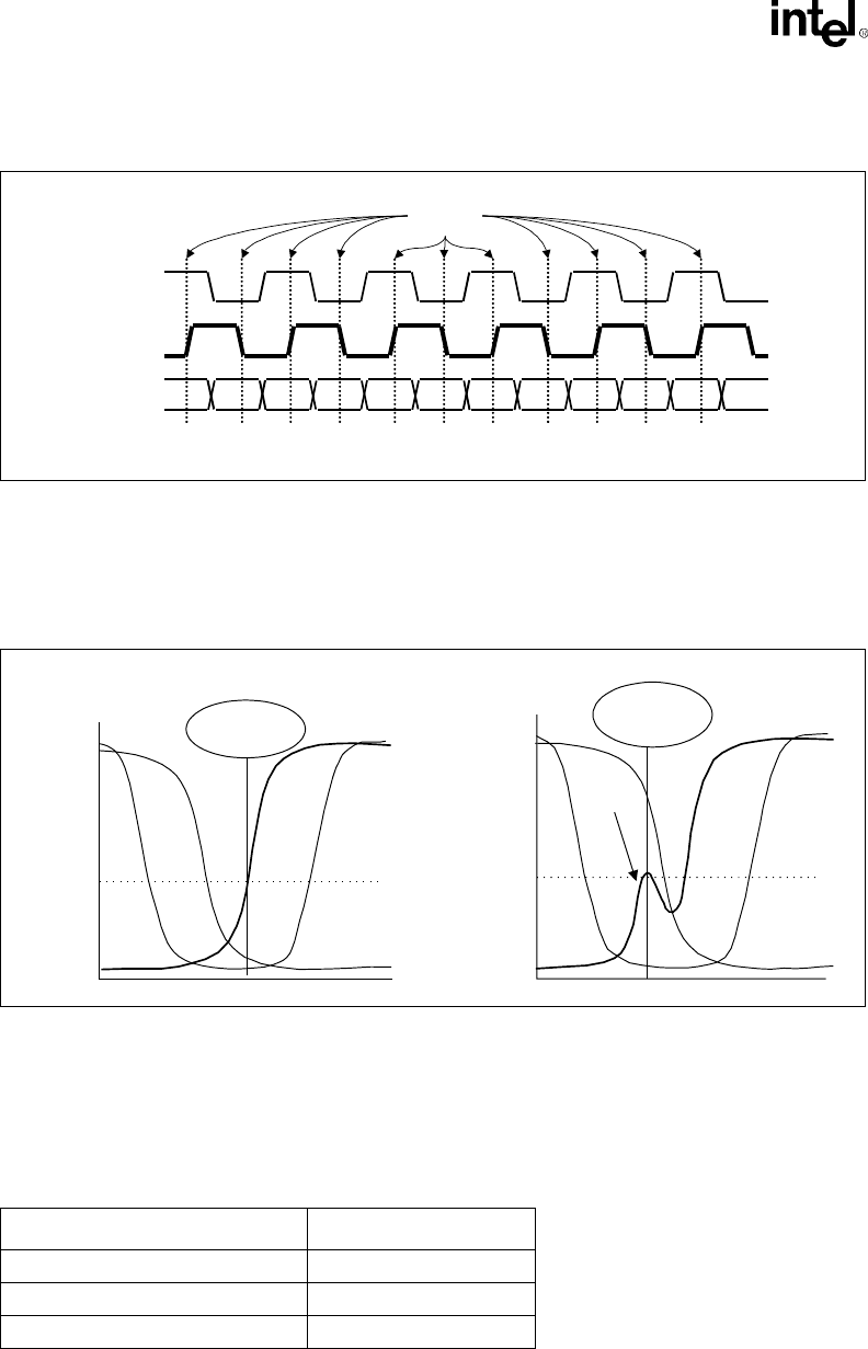
2.5 Source Synchronous Strobing
Source synchronous strobing is one of the technologies used in AGP 4X, Direct RDRAM and hub
interface that allow very high data transfer rates. As buses get faster, and cycle times get shorter,
the propagation delay is becoming a limiting factor in bus speed. Source synchronous strobing is
used to minimize the impact of propagation delay (Tprop) on maximum bus frequency.
A source synchronous strobed interface uses strobe signals (instead of the clock) to indicate that
data is valid. Refer to Figure 2-6 for an example.
Figure 2-5. Secondary Side MCH Core Routing Example (ATX)
Layout/Routing Guidelines
2-6 Intel®820 Chipset Design Guide
For a source synchronous strobed interface, it is very important that the strobe signals are routed
carefully. These signals must be very clean (free of noise). Data signals are typically latched on the
rising or falling edge of the strobe signal (or both). If there is noise on these signals, it could cause
an extra “edge” to be detected, thus latching incorrect data. Refer to Figure 2-7 for examples.
Some buses have more than one strobe (i.e., AGP). The AGP 1.0 specification (1X and 2X mode)
employs 3 strobe signals. These three strobe signals are each used to strobe different data signals.
That is, each strobe has an associated set of data signals. The associations for AGP 1.0 (AGP 2X)
are documented in Table 2-1. Refer to Section 2.7, “AGP 2.0” on page 2-31 for more information
on AGP 2.0 (AGP 4X, 1.5v).
In this example, the lower address signals (AD[15:0]) are sampled on the rising and falling edges
of AD_STB0, while the upper address signals (AD[31:16]) are sampled on the rising and falling
edges of AD_STB1.
Figure 2-6. Data Strobing Example
Clock
Strobe
Data
Data
Sample
data_str.vsd
Figure 2-7. Effect of Crosstalk on Strobe Signal
clock
Data
Threshold
Strobe
Data is correctly
latchecd as a "0"
clock
Data
Threshold
Strobe
Noise
(i.e.,
crosstalk)
Data is incorrectly
latchecd as a "1"
a) Correct Strobing Example (no noise) b) Effect of Crosstalk on Strobe Signal
Table 2-1. AGP 2X Data/Strobe Association
Data Associated Strobe
AD[15:0] and C/BE[1:0]# AD_STB0
AD[31:16] and C/BE[3:2]# AD_STB1
SBA[7:0] SB_STB
Intel®820 Chipset Design Guide 2-7
Layout/Routing Guidelines
When routing strobes and their associated data lines, trace length mismatch is very important (in
addition to noise immunity). The primary benefit of source synchronous strobing is that the data
and the strobe arrive at the receiver simultaneously. Thus, a strobe and its associated data signals
have very critical length mismatch requirements. With well matched trace lengths (as well as
matched impedance), the propagation delay for the strobe, and the propagation delay for the data
will be very close. Hence, the strobe and the data arrive at the receiver simultaneously. For some
interfaces, the trace length mismatch requirement is less than 0.25 inch.
2.6 Direct Rambus* Interface
The Direct Rambus* Channel is a multi-symbol interconnect. Due to the length of the interconnect
and the frequency of operation, this bus is designed to allow multiple command and data packets to
be present on a signal wire at any given instant. The driving device sends the next data out before
the previous data has left the bus.
The nature of the multi-symbol interconnect forces many requirements on the bus design and
topology. First and foremost, a drastic reduction in reflected voltage levels is required. The
interconnect transmission lines must be terminated at their characteristic impedance, or the
reflected voltage resulting from a mismatch in impedance will degrade signal quality. These
reflections will reduce noise and timing margins, and reduce the maximum operating frequency of
the bus. Potentially, the reflections could create data errors.
Due to the tolerances of components such as PCBs, connectors, and termination resistors, there will
be some reflected voltage on the interconnect. In this multi-symbol interconnect, timings are
pattern dependent due to the reflections interfering with the next transfer.
Additionally, coupled noise can greatly affect the performance of high-speed interfaces. Just as in
source synchronous designs, the odd and even mode propagation velocity change creates skew
between the clock and data or command lines which reduces the maximum operating frequency of
the bus. Efforts must be made to significantly decrease crosstalk, as well as the other sources of
skew.
To achieve these bus requirements, the Direct Rambus* channel is designed to operate as a
transmission line; all components, including the individual RDRAMs, are incorporated into the
design to create a uniform bus structure that can support up to 33 devices (including the MCH)
running at 800 MegaTransfers/second (MT/s).
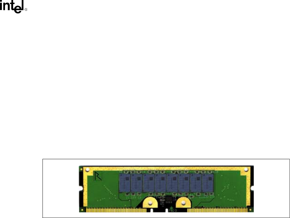
Figure 2-8. RIMM Diagram

Layout/Routing Guidelines
2-8 Intel®820 Chipset Design Guide
2.6.1 Stackup
The perfect matching of transmission line impedance and uniform trace length are essential for the
Direct RDRAM interface to work properly. Maintaining 28 Ω (±10%) loaded impedance for every
RSL (Direct Rambus* Signaling Level) signal has changed the requirements for trace width and
prepreg thickness for the Intel® 820 chipset platform (refer to Section 5.3, “Stackup Requirement”
on page 5-1).
Achieving a 28 Ω nominal impedance with a traditional 7 mil prepreg requires 28 mil wide traces.
These traces are too wide to break out of the two rows of RSL balls on the MCH. To reduce trace
width, a 4.5 mil thick prepreg is required. This thinner prepreg allows 18 mil wide traces to meet
the 28 Ω (±10%) nominal impedance requirement. Refer to Section 5.3, “Stackup Requirement” on
page 5-1 for detailed stackup requirements.
2.6.2 Direct Rambus* Layout Guidelines
The signals on the Direct Rambus* Channel are broken into three groups: RSL signals, CMOS
signals, and Clocking signals. The signal groups are:
•RSL Signals
— DQA[8:0]
—DQB[8:0]
—RQ[7:0]
•CMOS Signals
— CMD (high-speed CMOS signal)
— SCK (high-speed CMOS signal)
—SIO
•Clocking Signals
—CTM, CTM#
—CFM, CFM#
2.6.2.1 RSL Routing
The RSL signals enter the first RIMM on the left side, propagate through the RIMM, and exit on
the right. The signal continues through the rest of the existing RIMMs until it is terminated at
Vterm. All unpopulated slots must have continuity modules in place to ensure that the signals
propagate to the termination.
Intel®820 Chipset Design Guide 2-9
Layout/Routing Guidelines
To maintain a nominal 28 Ω trace impedance, the RSL signals must be 18 mils wide. To control
crosstalk and odd/even mode velocity deltas, there must be a 10 mil ground isolation trace routed
between adjacent RSL signals. The 10 mil ground isolation traces must be connected to ground
with a via every 1”. A 6 mil gap is required between the RSL signals and the ground isolation trace.
These signals must be length matched to ±10 mils in line section “A” and ±2 mils in both line
sections labeled “B” using the trace length matching methods in Section 2.6.2.6, “Length Matching
Methods” on page 2-21. To ensure uniform trace lines, trace width variation must be uniform on all
RSL signals at every neck-down for each line section. All RSL signals must have the same number
of vias. It may be necessary to place vias on RSL signals where they are not necessary to meet this
via loading requirement (i.e., dummy vias).
Figure 2-10 shows a top view of the trace width/spacing requirements for the RSL signals.
Figure 2-9. RSL Routing Dimensions
MCH
MCH to
First RIMM
RIMM_0 RIMM_1
A B C
RIMM to
RIMM RIMM to
Termination
0"-3.50" 0.4"-0.45" 0"-3"
Table 2-2. Placement Guidelines for Motherboard Routing Lengths
Reference Trace Description Maximum Trace Length (in.)
A MCH to first RIMM Connector 0” to 3.50”
B RIMM to RIMM 0.4” – 0.45”
C RIMM to Termination 0” to 3”
Figure 2-10. RSL Routing Diagram
RSL Signal Trace
Space
Ground
Space
RSL Signal Trace
Space
Ground
Space
18 mils
6 mils
10 mils
10 mils
6 mils
6 mils
18 mils
6 mils
Layout/Routing Guidelines
2-10 Intel®820 Chipset Design Guide
Figure 2-11 and Figure 2-12 show a top view of an example RSL breakout and route.
Figure 2-11. Primary Side RSL Breakout Example
Neckdown to
pass vias
BJT
14 on 6
Differential
clock pair
Ground Flood
(Shaded area)
18 mil clock
traces when
not 14:6
Neckdown for BJT
Intel®820 Chipset Design Guide 2-11
Layout/Routing Guidelines
2.6.2.2 RSL Termination
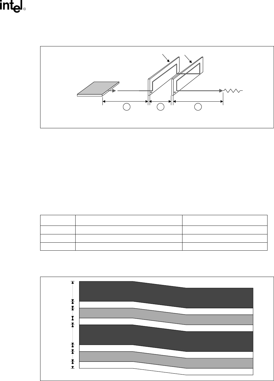
All RSL signals must be terminated to 1.8V (Vterm) using 27Ω-2% or 28Ω-1% resistors at the end
of the channel opposite the MCH. Resistor packs are acceptable. Vterm must be decoupled using
high speed bypass capacitors (one 0.1 µF ceramic chip capacitor per two RSL lines) near the
terminating resistors. Additionally, bulk capacitance is required. Assuming a linear regulator with
approximate 20 ms response time, two 100 µF tantalum capacitors are recommended. The trace
length between the last RIMM and the termination resistors should be less than 3”. Length
matching in this section of the channel is not required. The Vterm power island should be at
LEAST 50 mils wide. This voltage does not need to be supplied during suspend-to-RAM.
Figure 2-12. Secondary Side RSL Breakout Example
Figure 2-13. Direct RDRAM Termination
RSL Signals
Terminator
R-packs
Vterm
Layout/Routing Guidelines
2-12 Intel®820 Chipset Design Guide
Note: It is necessary to compensate for the slight difference in electrical characteristics between a dummy
via and a real via. Refer to Section 2.6.2.7, “VIA Compensation” on page 2-23 for more
information on Via Compensation.
Figure 2-14. Direct Rambus* Termination Example
2 GND VIAS /
Capacitor
Intel®820 Chipset Design Guide 2-13
Layout/Routing Guidelines
2.6.2.3 Direct Rambus* Ground Plane Reference
All RSL signals must be referenced to GND to provide an optimal current return path. The direct
Rambus ground plane reference must be continuous to the Vterm capacitors. The ground reference
island under the RSL signals must be continuous from the last RIMM to the back of the termination
capacitors. Choose the reference island shape such that power delivery to the components is not
compromised. The return current will flow through the Vterm capacitors into the ground island and
under the RSL traces. Any split in the ground island will provide a sub-optimal return path. In a 4
layer board, this will require the Vterm island to be on an outer layer. The Vterm island should
ALWAYS be placed on the top layer. Refer to Section 6.2, “Power Plane Splits” on page 6-7 for an
example of power plane splits.
The ground reference island under the RSL signals MUST be connected to the ground pins on the
RIMM connector and the ground vias used to connect the ground isolation on the 1st and 4th layers.
Figure 2-15. Incorrect Direct Rambus* Ground Plane Referencing
Figure 2-16. Direct Rambus Ground Plane Reference
3.3V Plane
1.8V Plane
MCH Wrong
Wrong
RIMM2
RIMM1
Extend GND PLANE
Reference Island Beyond
Vterm Capacitors
GND Plane 1.8V Plane
RIMM1
GND PlaneGND Plane
MCH
Required
Vterm Layer Not Shown
Vterm Resistors
Vterm Capacitors
RIMM2
3.3V Plane

Layout/Routing Guidelines
2-14 Intel®820 Chipset Design Guide
All 4 layers of the motherboard require correct grounding between the RSL signals on the
motherboard:
•Layer 1 = Ground Isolation
•Layer 2 = Ground Plane
•Layer 3 = Ground Reference in the Power Plane
•Layer 4 = Ground Isolation
All ground vias and pins MUST be connected to all 4 layers.
2.6.2.4 Direct Rambus* Connector Compensation
The RIMM connector inductance causes an impedance discontinuity on the Direct Rambus*
channel. This may reduce voltage and timing margin.
To compensate for the inductance of the connector, approximately 0.65 pF–0.85 pF compensating
capacitive tab (C-TAB) is required on each RSL connector pin. This compensating capacitance
must be added to the following connector pins at each connector:
LCTM LCTM#
RCTM RCTM#
LCFM LCFM#
RCFM RCFM#
LROW[2:0] RROW[2:0]
LCOL[4:0] RCOL[4:0]
RDQA[8:0] LDQA[8:0]
RDQB[8:0] LDQB[8:0]
SCK CMD
This can be achieved on the motherboard by adding a copper tab to the specified RSL pins at each
connector. The target value is approximately 0.65 pF–0.85 pF. The copper tab area for the
recommended stackup was determined through simulation. The placement of the copper tabs can
be on any signal layer, independent of the layer on which the RSL signal is routed.
Equation is an approximation that can be used for calculating copper tab area on an outer layer.
Equation 2-1. Approximate Copper Tab Area Calculation
Length*Width = Area = Cplate * Thickness of prepreg / [(ε0) (εr) (1.1)]
Where:
—ε0 = 2.25 x 10⁻¹⁶ Farads/mil
—εr = Relative dielectric constant of prepreg material
— Thickness of prepreg = Stackup dependent
— Length, Width = Dimensions in mils of copper plate to be added
— Factor of 1.1 accounts for fringe capacitance.
Based on the stackup requirement in Section 5.3, “Stackup Requirement” on page 5-1 the copper
tab area should be 2800 to 3600 sq mils. Different stackups require different copper tab areas.
Table 2-3 shows example copper tab areas.

Intel®820 Chipset Design Guide 2-15
Layout/Routing Guidelines
Based on Equation 1, the tab area is 2800 sq mils, where εr is 4.2 and D is 4.5. These values are
based on 2116 prepreg material.
Note that more than one copper tab shape may be used. The tab dimensions are based on copper
area over the ground plane. The actual length and width of the tabs may be different due to routing
constraints (e.g., if tab must extend to center of hole, or antipad); however, each copper tab should
have equivalent area. For example, the copper tabs in Figure 2-17 have the following dimensions,
when measured tangent to the antipad:
Inner C-TAB = 140 (length) x 20(width)
Outer C-TAB = 70 (length) x 40 (width)
The following figures show a routing example of tab compensation capacitors. Note that ground
floods around the RIMM pins must not be interrupted by the capacitor tabs, and they must be
connected to avoid discontinuity in the ground plane as shown.
Table 2-3. Copper Tab Area Calculation
Dielectric
Thickness
(D)
Separation
Between
Signal Trace &
Copper Tab
Minimum
Ground
flood
Air Gap
between
Signal &
GND Flood
Compen-
sating
Capacitance
in pF
Copper Tab
(C-TAB)
Area (A) In
sq mils
C-TAB
Shape
(mils)
4.5 6 10 6 0.65 2800 140 L x 20 W
70 L x 40 W
Layout/Routing Guidelines
2-16 Intel®820 Chipset Design Guide
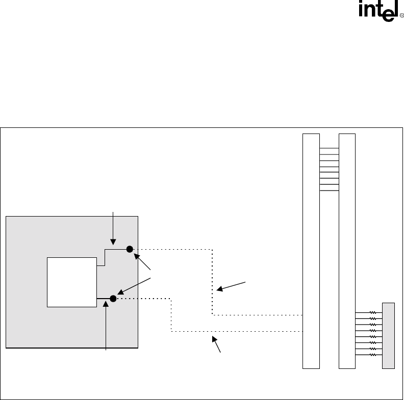
Figure 2-17. Connector Compensation Example
S
E
C
T
I
O
N
A
MCH
S
E
C
T
I
O
N
B
Intel®820 Chipset Design Guide 2-17
Layout/Routing Guidelines
NOTES:
1. Refer to Figure 2-17. Ground flood removed from picture for clarity
Figure 2-18. Section A1, Top Layer
Inner C-tab
Outer C-tab
Layout/Routing Guidelines
2-18 Intel®820 Chipset Design Guide
NOTES:
1. Refer to Figure 2-17. Ground flood removed from picture for clarity
Figure 2-19. Section A1, Bottom Layer
Intel®820 Chipset Design Guide 2-19
Layout/Routing Guidelines
NOTES:
1. Refer to Figure 2-17. Ground flood removed from picture for clarity
Figure 2-20. Section B1, Top Layer
Layout/Routing Guidelines
2-20 Intel®820 Chipset Design Guide
NOTES:
1. Refer to Figure 2-17. Ground flood removed from picture for clarity
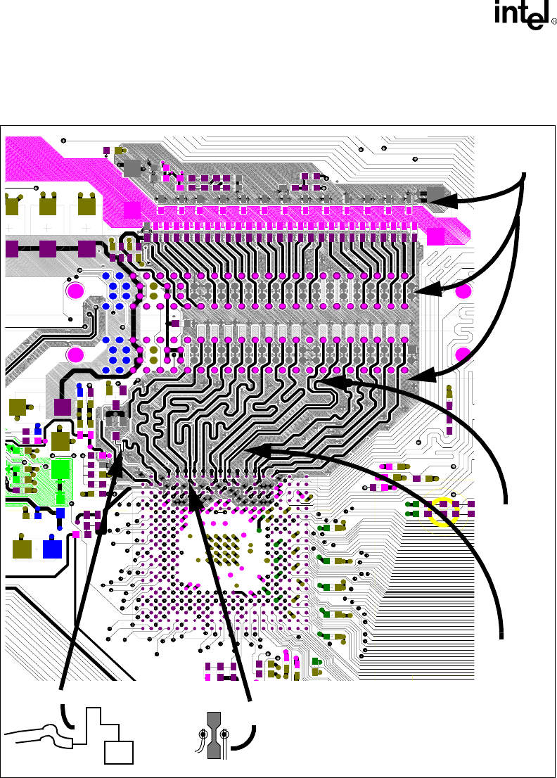
2.6.2.5 RSL Signal Layer Alternation
RSL signals must alternate layers as they are routed through the channel. If a signal is routed on the
primary layer from the MCH to the first RIMM socket, it must be routed on the secondary layer
from the first RIMM to the second RIMM as shown in Figure 2-22 (signal B). If a signal is routed
on the secondary layer from the MCH to the first RIMM socket, it must be routed on the primary
layer from the first RIMM to the second RIMM as shown in Figure 2-22 (signal A). Signals to the
termination resistors can be routed on either layer from the last RIMM.
Figure 2-21. Section B1, Bottom Layer
Intel®820 Chipset Design Guide 2-21
Layout/Routing Guidelines
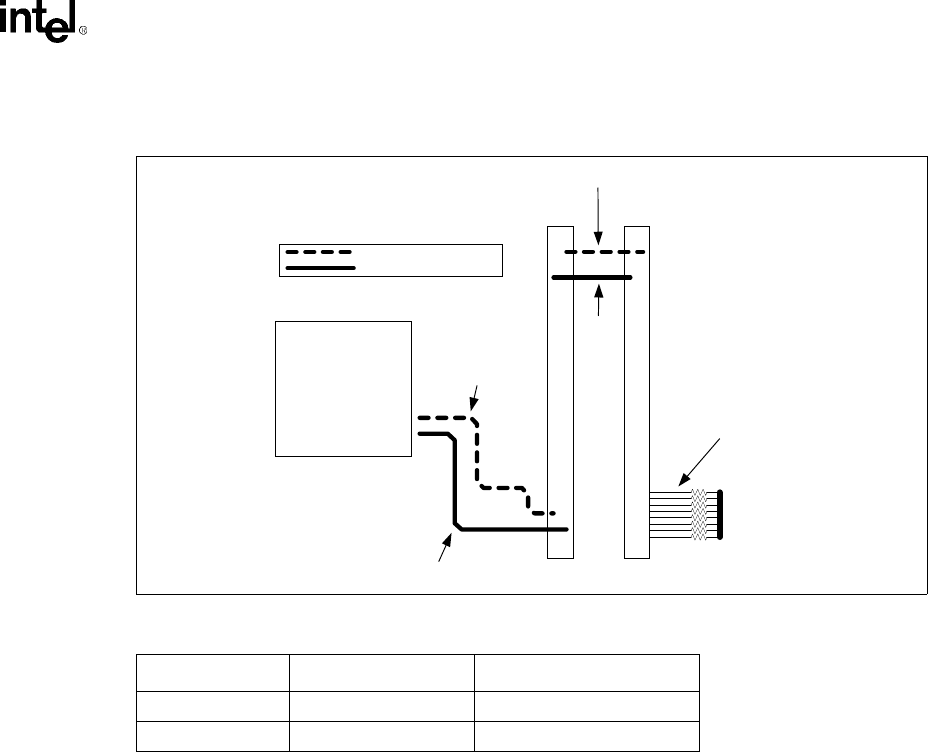
2.6.2.6 Length Matching Methods
In order to allow for greater routing flexibility, the RSL signals require pad-to-pin length matching
between the MCH and the first connector. If the trace lengths are matched between the balls of the
MCH and the pin of RIMM connector, the length mismatch between the pad (on the die) and the
ball has not been accounted. However, given the package dimension, a representation of the length
from the pad to the ball, the routing can compensate for this package mismatch. Therefore, the
board length mismatch can be increased.
The RSL channel requires matching trace lengths from pad-to-pin within ±10 mils.
Given these definitions:
•Package Dimension: a representation of the length from the pad to the ball.
•Board Trace Length: the trace length on the board.
•Nominal RSL Length: the length to which all signals are matched. (note: there is not
necessarily a trace that is EXACTLY to nominal length, but all RSL signals must be matched
to within ±10mil of a nominal length). The Nominal RSL Length is an arbitrary length (within
the limits of the routing guidelines) to which all the RSL signals will be matched (within
10 mils).
ALL RSL signals must meet the following equation.
Figure 2-22. RSL Signal Layer Alternation
Table 2-4. RSL Routing Layer Requirements
MCH to 1st RIMM 1st RIMM to 2nd RIMM
Method 1 Primary Side Secondary Side
Method 2 Secondary Side Primary Side
MCH
Signal on Secondary Side
Signal on Primary Side
Signal A
Signal B
Signal A
Signal B
Route on EITHER layer.
Ground Isolation is
REQUIRED!
Term
Layout/Routing Guidelines
2-22 Intel®820 Chipset Design Guide
Equation 2-2. RDRAM RSL Signal Trace Length Calculation
Package Dimension + Board Trace Length = Nominal RSL Length ± 10mils
NOTE: Refer to the Intel® 820 Chipset: Intel® 82820 Memory Controller Hub (MCH) Datasheet for component
package dimensions.
The RDRAM clocks (CTM, CTM#, CFM and CFM#) must be longer than the RDRAM signals
due to their increased trace velocity (because they are routed as a differential pair). To calculate the
length for each clock, the following formula should be used:
Equation 2-3. RDRAM Clock Signal Trace Length Calculation
Clock Length = Nominal RSL Signal Length (package + board) * 1.021
Using this formula, the clock signals will be 21 mils/inch longer than the Nominal Length. The
lengthening of the clock signals, to compensate for their trace velocity change, ONLY applies to
routing between the MCH and the first RIMM. The clock signals should be matched in length to
the RSL signals between RIMMs. Refer to Chapter 4, “Clocking” for more detailed clock routing
guidelines.
The high-speed CMOS signals must be length matched to the RSL signals within 1200 mils
(1.2 in) due to a timing requirement between CMOS and RSL signals during NAP Exit and PDN
Exit.
It is necessary to compensate for the slight difference in electrical characteristics between a dummy
via and a real via. Refer to the following section for more information on Via Compensation.
Figure 2-23. RDRAM Trace Length Matching Example
MCH
Die
MCH
Die
MCH Package
R
I
M
M
C
o
n
n
e
c
t
o
r
L3
L4
L1
L2
L1, L2 -> Package Dimensions
L3, L4 -> Board Trace Length
L1 + L3 = Nominal RSL Length ±10 mils
L2 + L4 = Nominal RSL Length ±10 mils
Ball
R
I
M
M
C
o
n
n
e
c
t
o
rV
t
e
r
m
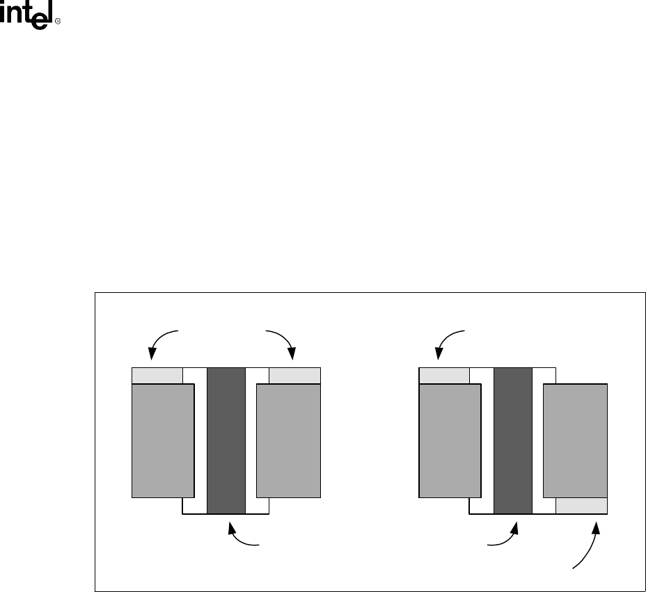
Intel®820 Chipset Design Guide 2-23
Layout/Routing Guidelines
2.6.2.7 VIA Compensation
As described in Section 2.8.2, “Strobe Signals” on page 2-44, all signals must have the same
number of vias. As a result, each trace will have 1 via (near the BGA pad) because some of the
RSL signals must be routed on the bottom of the motherboard. Therefore, it is necessary to place a
dummy via on all signals that are routed on the top layer. Because the electrical characteristics of a
dummy via do not match the electrical characteristics of a real via exactly, additional compensation
must be performed on each signal that has a dummy via. Each signal with a dummy via must have
25 mils of additional trace length. That is: a real via = a dummy via + 25 mils of trace length.
This 25 mils of additional trace length must be added to each signal routed on the top layer after
length matching, as documented in Section 2.6.2.6, “Length Matching Methods” on page 2-21.
2.6.2.8 Length Matching & Via Compensation Example
Table 2-5 can be used to ensure that the RSL signals are the correct length.
Note: 2000 mils was chosen as an EXAMPLE Nominal RSL Length.
Figure 2-24. "Dummy" Via vs. Real "Via"
“DUMMY Via”
PCB PCB
“REAL Via”
PCB PCB
Trace Trace
Via Via
Trace

Layout/Routing Guidelines
2-24 Intel®820 Chipset Design Guide
NOTES:
1. Signals connecting to the "A" side of the RIMM connector (i.e., A1, A2, A3, etc.) should be routed on the top
(primary side) of the motherboard;
2. Signals connecting to the "B" side of the RIMM connector should be routed on bottom (solder side).
3. These trace lengths ONLY apply from MCH to the 1st RIMM. All signals must match EXACTLY from RIMM to
RIMM.
4. Clock trace lengths include 1.021 trace velocity factor.
5. Formula A min: Motherboard Trace = (Nominal RSL Length - Package Dimension) - 10 mil
6. Formula A max: Motherboard Trace = (Nominal RSL Length - Package Dimension) + 10 mil
7. Formula B min: Motherboard Trace = (Nominal RSL Length - Package Dimension) - 10 mil + 25 mil
8. Formula B max: Motherboard Trace = (Nominal RSL Length - Package Dimension) + 10 mil + 25 mil
9. Formula C: Motherboard Trace = (Nominal RSL Length - Package Dimension) * 1.021
10.Formula D: Motherboard Trace = (Nominal RSL Length - Package Dimension + 25 mil) * 1.021
Table 2-5. Line Matching and Via Compensation Example1,2,3,4,5,6,7,8,9,10
Signal Ball
on
MCH
Nominal
RSL
Length
(mils)
Package
Dimension
(mils)
Motherboard Trace
Length when
Routed on Bottom
(i.e., Real Via)
Motherboard Trace
Length when
Routed on Top
(i.e., Dummy Via) Recommended
To Route On
Min
(mils) Max
(mils) Min
(mils) Max
(mils)
Formula A Formula B
DQA0 A13 2000 138.14 1851.86 1871.86 1876.86 1896.86 Top
DQA1 C13 2000 19.11 1970.89 1990.89 1995.89 2015.89 Bottom
DQA2 A14 2000 163.16 1826.84 1846.84 1851.84 1871.84 Top
DQA3 C14 2000 39.87 1950.13 1970.13 1975.13 1995.13 Bottom
DQA4 B14 2000 97.54 1892.46 1912.46 1917.46 1937.46 Top
DQA5 C15 2000 62.67 1927.33 1947.33 1952.33 1972.33 Bottom
DQA6 A15 2000 186.11 1803.90 1823.90 1828.90 1848.90 Top
DQA7 C16 2000 95.70 1894.30 1914.30 1919.30 1939.30 Bottom
DQA8 A16 2000 230.20 1759.81 1779.81 1784.81 1804.81 Top
DQB0 C7 2000 39.56 1950.44 1970.44 1975.44 1995.44 Bottom
DQB1 B7 2000 95.83 1894.17 1914.17 1919.17 1939.17 Top
DQB2 C6 2000 63.49 1926.51 1946.51 1951.51 1971.51 Bottom
DQB3 A6 2000 153.69 1836.31 1856.31 1861.31 1881.31 Top
DQB4 C5 2000 97.33 1892.67 1912.67 1917.67 1937.67 Bottom
DQB5 A5 2000 191.43 1798.57 1818.57 1823.57 1843.57 Top
DQB6 B5 2000 152.47 1837.53 1857.53 1862.53 1882.53 Bottom
DQB7 A4 2000 237.71 1752.29 1772.29 1777.29 1797.29 Top
DQB8 C4 2000 138.29 1851.71 1871.71 1876.71 1896.71 Bottom
RQ0 A7 2000 179.49 1810.51 1830.51 1835.51 1855.51 Top
RQ1 C8 2000 27.12 1962.88 1982.88 1987.88 2007.88 Bottom
RQ2 A8 2000 162.21 1827.79 1847.79 1852.79 1872.79 Top
RQ3 C9 2000 5.80 1984.20 2004.20 2009.20 2029.20 Bottom
RQ4 B9 2000 71.70 1918.30 1938.30 1943.30 1963.30 Top
RQ5 A9 2000 133.88 1856.12 1876.12 1881.12 1901.12 Bottom
RQ6 A10 2000 122.20 1867.81 1887.81 1892.81 1912.81 Top
RQ7 C10 2000 0.00 1990.00 2010.00 2015.00 2035.00 Bottom
FORMULA C FORMULA D
CFM A12 2000 132.37 1906.85 1932.37 Bottom
CFM# B12 2000 64.63 1976.02 2001.54 Bottom
CTM B11 2000 56.06 1984.76 2010.29 Top
CTM# A11 2000 126.34 1913.01 1938.53 Top
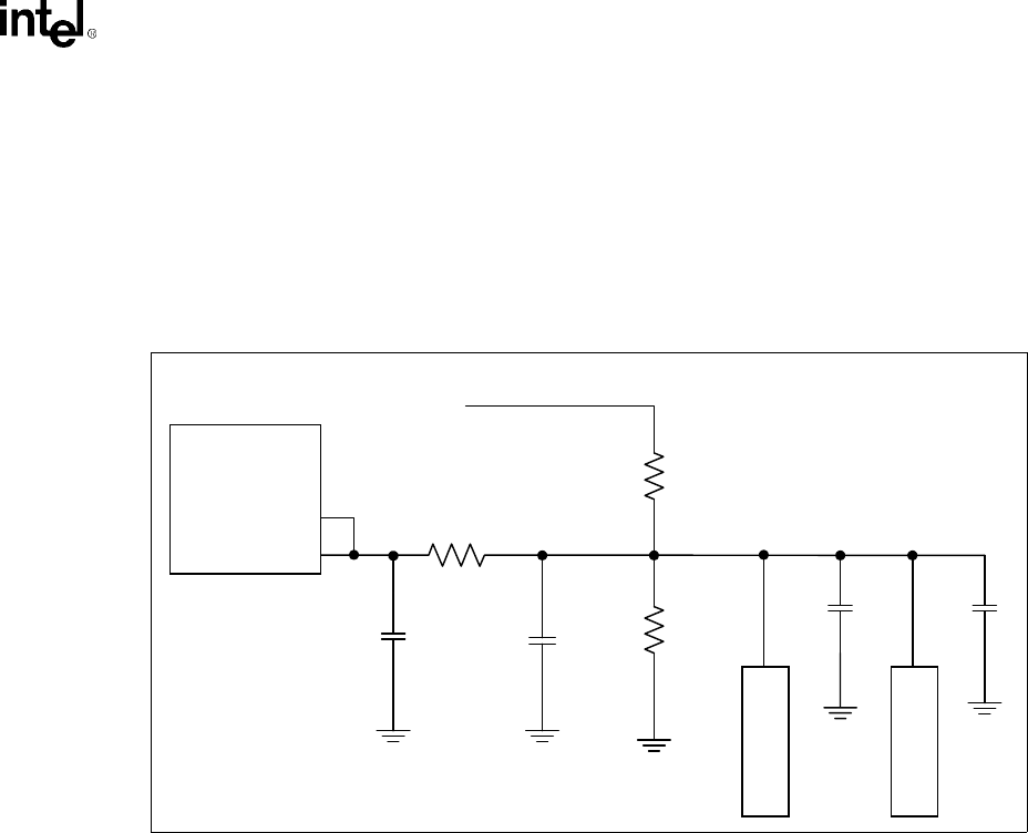
Intel®820 Chipset Design Guide 2-25
Layout/Routing Guidelines
2.6.3 Direct Rambus* Reference Voltage
The Direct Rambus* reference voltage (RAMREF) must be generated as shown in Figure 2-25.
RAMREF should be generated from a typical resistor divider using 2% tolerance resistors.
Additionally, RAMREF must be decoupled locally at EACH RIMM connector, at the resistor
divider and at the MCH. Finally, as shown in Figure 2-25, a 100 Ω series resistor is required near
the MCH. The RAMREF signal should be routed with a 10 mil wide trace.
2.6.4 High-speed CMOS Routing
•The high-speed CMOS signals (CMD & SCK) must be routed using 28 Ω traces. Using the
recommended stackup, these signals will be 18 mils wide.
•The high-speed CMOS signals must be length matched to the RSL signals within 1200 mils
(1.2in) due to a timing requirement between CMOS and RSL signals during NAP Exit and
PDN Exit.
•The high-speed CMOS signals require termination as shown in Figure 2-26 due to the buffer
strengths in the MCH.
•The resistors must be 91 Ω pullup and 39 Ω pulldown; they also must 2% or better for S3
mode reliability. The trace impedances remain 28 Ω.
Figure 2-25. RAMRef Generation Example Circuit
160
Ω
2%
R
I
M
M
Vterm
R3
C4 C10
C5 C8
0.1 uF 0 .1 uF
100 Ω
R1
R2 0.1 uF
0.1 uF
R
I
M
M
560
Ω
2%
RAMREFA
RAMREFB
MCH
Layout/Routing Guidelines
2-26 Intel®820 Chipset Design Guide
2.6.4.1 SIO Routing
The SIO signal must be routed from RIMM to RIMM as shown in Figure 2-17. The SIO signal
requires a 2.2 KΩ – 10 KΩ terminating resistor on the SOUT pin of the last RIMM. SIO is routed
with a standard 5 mil wide 60 Ω trace. The motherboard routing lengths for the SIO signal are the
same as RSL signals (see Figure 2-17).
2.6.4.2 Suspend-to-RAM Shunt Transistor
When an Intel® 820 chipset system enters or exits Suspend-to-RAM, power will be ramping to the
MCH (i.e., it will be powering-up or powering-down). When power is ramping, the state of the
MCH outputs is not guaranteed. Therefore, the MCH could drive the CMOS signals and issue
CMOS commands. One of the commands (the only one the RDRAMs would respond to) is the
powerdown exit command. To avoid the MCH inadvertently taking the RDRAMs out of power-
down due to the CMOS interface being driven during power ramp, the SCK (CMOS clock) signal
must be shunted to ground when the MCH is entering and exiting Suspend-to-RAM. This shunting
can be accomplished using the NPN transistor shown in circuit shown in Figure 2-28. The
transistor should have a Cobo of 4 pf or less (i.e., MMBT3904LT1).
In addition, to match the electrical characteristics on the SCK signal, the CMD signal needs a
dummy transistor. This transistor’s base should be tied to ground (i.e., always turned off).
Figure 2-26. High-Speed CMOS Termination
MCH
RIMM_0 RIMM_1
91
Ω
Vterm
39
Ω
R1
R2
Figure 2-27. SIO Routing Example
A
B
0" - 3.50" 0.4" - 0.45"
SIN B36
SIN B36
A36 SOUT
A36 SOUT
2.2KΩ -
10KΩ
82820
MCH
N
3
2
1
N
3
2
1
Intel®820 Chipset Design Guide 2-27
Layout/Routing Guidelines
To minimize impedance discontinuities, the traces for CMD and SCK must have a neckdown from
18 mil traces to 5 mil traces for 175 mils on either side of the SCK/CMD attach point as shown in
Figure 2-28.
Figure 2-28. RDRAM CMOS Shunt Transistor
175 mils
PWROK
SCK
MCH
2N3904
18 mils
wide
175 mils
MCH
18 mils
wide 18 mils
wide
5 mils
wide
175
mils
175
mils
CMD
2N3904
2N3904
VCC5SBY
5 mils
wide
18 mils
wide
R
I
M
M
S
R
I
M
M
S

Layout/Routing Guidelines
2-28 Intel®820 Chipset Design Guide
2.6.5 Direct Rambus* Clock Routing
Refer to Chapter 4, “Clocking” for Intel® 820 chipset platform Direct Rambus* clock routing
guidelines.
2.6.6 Direct Rambus* Design Checklist
Use the following checklist as a final check to ensure the motherboard incorporates solid design
practices. This list is only a reference. For correct operation, all of the design guidelines within this
document must be followed.
•Ground Isolation Well Grounded
— Via to ground every ½ inch around edge of isolation island
— Via to ground every ½ inch between RIMMs
— Via to ground every ½ inch between signals (from MCH to first RIMM)
— Via between every signal within 100mils of the MCH edge and the connector edge
— No unconnected ground floods
— All ground isolation at least 10 mils wide
— Ground isolation fills between serpentines
— Ground isolation not broken by C-TABs
— Ground isolation connects to the ground pins in the middle of the RIMM connectors
— Ground isolation vias connect on all 4 layers and should NOT have thermal reliefs
— Ground pins in RIMM connector connect on all 4 layers
•Vterm Layout Yields Low Noise
— Solid Vterm island is on top layer – do not split this plane
— Ground island (for ground side of Vterm caps) is on top
— Termination Resistors connect DIRECTLY to the Vterm island on the top layer (without
vias)
— Decoupling Vterm is CRITICAL!
— Decoupling capacitors connect to top layer Vterm island and top layer ground island
directly (see layout example)
— Use AT LEAST 2 vias per decoupling capacitor in the top layer ground island
— Use 2 x 100 uF TANTALUM capacitors to decouple Vterm
(Aluminum/Electrolytic capacitors are too slow!)
— High-frequency decoupling capacitors MUST be spread-out across the termination island
so that all termination resistors are near high-frequency capacitors
— 100uF TANTALUM capacitors should be at each end of the Vterm island
— 100uF TANTALUM capacitors must be connected to Vterm island directly
— 100uF TANTALUM capacitors must have AT LEAST 2 vias/cap to ground
Table 2-6. Signal List
RSL Signals High-Speed
CMOS Signals Serial CMOS Signal Clocks
DQA[8:0]
DQB[8:0]
RQ[7:0]
CMD
SCK SIO
CTM
CTM#
CFM
CFM#

Intel®820 Chipset Design Guide 2-29
Layout/Routing Guidelines
— Vterm island should be 50 – 75 mils wide
— Vterm island should not be broken
— If any RSL signals are routed out of the last RIMM (towards termination) on the bottom
side (even for a short distance), ensure Ground Reference Plane (on the third layer) is
continuous under the termination resistors/capacitors
— Ensure current path for power delivery to the MCH does not go through the Vterm island
•CTM/CTM# Routed Properly
— CTM/CTM# are routed differentially from DRCG to last RIMM
— CTM/CTM# are ground isolated from DRCG to last RIMM
— CTM/CTM# are ground referenced from DRCG to last RIMM
— Vias are placed in ground isolation and ground reference every ½”
— When CTM/CTM# serpentine together, they MUST maintain EXACTLY 6 mils spacing
•Clean DRCG Power Supply
— 3.3V DRCG power flood on the top layer. This should connect to each
— High frequency (0.1 uF) capacitors are near the DRCG power pins. One capacitor next to
each power pin.
— 10uF bulk tantalum capacitor near DRCG connected directly to the 3.3V DRCG power
flood on the top layer
— Ferrite bead isolating DRCG power flood from 3.3V main power also connecting directly
to the 3.3VDRCG power flood on the top layer
— Use 2 vias on the ground side of each
•Good DRCG Output Network Layout
— Series resistors (39 Ω) should be VERY near CTM/CTM# pins
— Parallel resistors (51 Ω) should be very near series resistors
— CTM/CTM# should be 18mils wide from the CTM/CTM# pins to the resistors
— CTM/CTM# should be 14 on 6 routed differential as soon as possible after the resistor
network
— When not 14 on 6, the clocks should be 18 mils wide
— Ensure CTM/CTM# are ground referenced and the ground reference is connected to the
ground plane every ½” to 1”
— Ensure CTM/CTM# are ground isolated and the ground isolation is connected to the
ground plane every ½” to 1”
— Ensure 15 pf EMI capacitors to ground are removed (the pads are not necessary and
removing the pads provides more space for better placement of other components)
— Ensure the 4 pf EMI capacitor is implemented (but do not assemble the capacitor)
•Good RSL Transmission Lines
— RSL traces are 18 mils wide
— When RSL traces neck down to exit MCH BGA, the minimum width is 15 mils and the
neckdown is no longer than 25 mils in length
— RSL traces do NOT neckdown when routing into the RIMM connector
— If tight serpentining is necessary, 10 mil ground isolation MUST be between serpentine
segments (i.e., an RSL signal CAN NOT serpentine so tightly that the signal is adjacent to
itself with no ground isolation between the serpentines).
— RSL traces do not cross power plane splits. RSL signals must also not be routed on next to
a power plane splits (e.g., the RSL signals on the 4th layer can not be routed directly below
the ground isolation split on the 3rd layer)
— Uniform ground isolation flood is exactly 6 mils from the RSL signals at all times

Layout/Routing Guidelines
2-30 Intel®820 Chipset Design Guide
— ALL RSL, CMD/SCK and CTM/CTM#/CFM/CFM# signals have CTABs on each RIMM
connector pin
— All RSL signals are routed adjacent to a ground reference plane. This includes all signals
from the last RIMM to the termination. If signals are routed on the bottom from the last
RIMM to the termination, the ground reference plane on the 3rd layer MUST extend under
these signals AND include the ground side of the Vterm decoupling capacitors.
— CTABs must not cross (or be on top of) power plane splits. They must be ENTIRELY
referenced to ground.
— At least 10 mils ground flood isolation required around ALL RSL signals (ground
isolation must be exactly 6 mils from RSL signals). Ground flood recommended for
isolation. This ground flood should be as close to the MCH (and the 1st RIMM) as
possible. If possible connect the flood to the ground balls/pins on the MCH/connector.
•Clean VREF Routing
— Ensure 1 x 0.1 uF capacitor on VREF at each connector
— Use 10 mil wide trace (6 mils minimum)
— Do not route VREF near high-speed signals
•RSL Routing
— All signals must be length matched within ±10 mils of the Nominal RSL Length (note:
use the table in the Intel® 820 chipset: 82820 Memory Controller Hub (MCH) Datasheet
to verify trace lengths). Ensure that signals with a dummy via are compensated correctly.
— ALL RSL signals must have 1 via near the MCH BGA pad. Signals routed on the
secondary side of the MB will have a “real via” while signals routed on the primary side
will have a “dummy via”. Additionally, all signals with a dummy via must have an
additional trace length of 25 mils.
— “B” side RIMM connector signals are routed on the secondary side of the motherboard.
“A” side RIMM connector signals are routed on the primary side of the motherboard.
— Signals must “alternate” layers as shown in the following table.
•Clock Routing
— Clock signals must be routed as a differential pair. The traces must be 14 mils wide and 6
mils apart (with no ground isolation) when they are routed as a differential pair. For very
short sections under the MCH and under the 1st RIMM, it will not be possible to route as
a differential pair. In these sections, the clocks signals MUST neck up to 18 mils and be
ground isolated with at least 10 mils ground isolation.
— Clock signals must be length compensated (using the 1.021 length factor described in
Section 2.7.3, “2X/4X Timing Domain Routing Guidelines” on page 2-33). Ensure that
each clock pair is length matched within ±2 mils.
— When clock signals serpentine, they must serpentine together (to maintain differential
14:6 routing).
— 22 mils ground isolation required on each side of the differential pair.
If Signal Routed from MCH to the 1st RIMM on: Then Route Signal from 1st RIMM to Next
RIMM on:
Primary Side Secondary Side
Secondary Side Primary Side

Intel®820 Chipset Design Guide 2-31
Layout/Routing Guidelines
2.7 AGP 2.0
For detailed AGP Interface functionality (protocols, rules and signaling mechanisms, etc.) refer to
the latest AGP Interface Specification revision 2.0, which can be obtained from http://
www.agpforum.org. This document focuses only on specific Intel® 820 chipset platform
recommendations.
The AGP Interface Specification revision 2.0 enhances the functionality of the original AGP
Interface Specification (revision 1.0) by allowing 4X data transfers (4 data samples per clock) and
1.5 volt operation. In addition to these major enhancements, additional performance enhancement
and clarifications, such as fast write capability, are included in the AGP Interface Specification,
Revision 2.0. The Intel® 820 chipset is the first Intel chipset that supports the enhanced features of
AGP 2.0.
The 4X operation of the AGP interface provides for “quad-pumping” of the AGP AD (Address/
Data) and SBA (Side-band Addressing) buses. That is, data is sampled four times during each
66 MHz AGP clock. This means that each data cycle is ¼ of a 15 ns (66 MHz) clock or 3.75 ns. It
is important to realize that 3.75 ns is the data cycle time, not the clock cycle time. During 2X
operation, data is sampled twice during a 66 MHz clock cycle; therefore, the data cycle time is
7.5 ns.
To allow for these high speed data transfers, the 2X mode of AGP operation uses source
synchronous data strobing (refer to Section 2.5, “Source Synchronous Strobing” on page 2-5).
During 4X operation, the AGP interface uses differential source synchronous strobing.
With data cycle times as small as 3.75 ns, and setup/hold times of 1 ns, propagation delay
mismatch is critical. In addition to reducing propagation delay mismatch, it is important to
minimize noise. Noise on the data lines will cause the settling time to be large. If the mismatch
between a data line and the associated strobe is too great, or there is noise on the interface,
incorrect data will be sampled.
The low-voltage operation on AGP (1.5V) requires even more noise immunity. For example,
during 1.5V operation, Vilmax is 570 mv. Without proper isolation, crosstalk could create signal
integrity issues.

Layout/Routing Guidelines
2-32 Intel®820 Chipset Design Guide
2.7.1 AGP Interface Signal Groups
The signals on the AGP interface are broken into three groups: 1X timing domain signals, 2X/4X
timing domain signals and miscellaneous signals. Each group has different routing requirements.
In addition, within the 2X/4X timing domain signals, there are three sets of signals. All signals in
the 2X/4X timing domain must meet minimum and maximum trace length requirements as well as
trace width and spacing requirements. However, trace length matching requirements only need to
be met within each set of 2X/4X timing domain signals.
Signal groups
•1X Timing Domain
— CLK (3.3V)
— RBF#
—WBF#
— ST[2:0]
—PIPE#
—REQ#
—GNT#
—PAR
—FRAME#
— IRDY#
— TRDY#
—STOP#
— DEVSEL#
•2X/4X Timing Domain
Set #1
— AD[15:0]
— C/BE[1:0]#
—AD_STB0
— AD_STB0# (used in 4X mode ONLY)
Set #2
— AD[31:16]
— C/BE[3:2]#
—AD_STB1
— AD_STB1# (used in 4X mode ONLY)
Set #3
—SBA[7:0]
—SB_STB
— SB_STB# (used in 4X mode ONLY)
•Miscellaneous, Async
—USB+
—USB-
—OVRCNT#
—PME#
— TYPDET#
—PERR#
—SERR#
— INTA#
—INTB#

Intel®820 Chipset Design Guide 2-33
Layout/Routing Guidelines
Throughout this section the term data refers to AD[31:0], C/BE[3:0]# and SBA[7:0]. The term
strobe refers to AD_STB[1:0], AD_STB#[1:0], SB_STB and SB_STB#. When the term data is
used, it is referring to one of the three sets of data signals. When the term strobe is used, it is
referring to one of the strobes as it relates to the data in its associated group.
The routing guidelines for each group of signals (1X timing domain signals, 2X/4X timing domain
signals and miscellaneous signals) will be addressed separately.
2.7.2 1X Timing Domain Routing Guidelines
•The AGP 1X timing domain signals (refer to Signal Groups previously shown) have a
maximum trace length of 7.5 inches. This maximum applies to ALL of the signals listed as 1X
timing domain signals in Signal Groups section.
•AGP 1X timing domain signals can be routed with 5 mil minimum trace separation.
•There are no trace length matching requirements for 1X timing domain signals.
2.7.3 2X/4X Timing Domain Routing Guidelines
These trace length guidelines apply to ALL of the signals listed as 2X/4X timing domain signals.
These signals should be routed using 5 mil (60 Ω) traces.
The maximum line length and length mismatch requirements are dependent on the routing rules
used on the motherboard. These routing rules were created to give design freedom by making
tradeoffs between signal coupling (trace spacing) and line lengths. The maximum length of the
AGP interface defines which set of routing guidelines must be used. Guidelines for short AGP
interfaces (e.g., < 6”) and the long AGP interfaces (e.g., > 6” and < 7.25”) are documented
separately. The maximum length allowed for the AGP interface is 7.25 inches.
Interfaces < 6”
If the AGP interface is less than 6 inches, a minimum 1:3 trace spacing is required for 2X/4X lines
(data and strobes). These 2X/4X signals must be matched their associated strobe within ±0.5
inches. These guidelines are for designs that require less than 6 inches between the AGP connector
and the MCH.
For example, if a set of strobe signals (e.g., AD_STB0 and AD_STB0#) are 5.3” long, the data
signals which are associated to those strobe signals (e.g., AD[15:0] and C/BE[2:0]#), can be 4.8” to
5.8” long. Another strobe set (e.g., SB_STB and SB_STB#) could be 4.2” long, and the data
signals which are associated to those strobe signals (e.g., SBA[7:0]), can be 3.7” to 4.7” long.
Table 2-7. AGP 2.0 Data/Strobe Associations
Data Associated
Strobe in 1X Associated
Strobe in 2X Associated
Strobes in 4X
AD[15:0] and
C/BE[1:0]# Strobes are not used in 1X mode. All data is
sampled on rising clock edges. AD_STB0 AD_STB0, AD_STB0#
AD[31:16] and
C/BE[3:2]# Strobes are not used in 1X mode. All data is
sampled on rising clock edges. AD_STB1 AD_STB1, AD_STB1#
SBA[7:0] Strobes are not used in 1X mode. All data is
sampled on rising clock edges. SB_STB SB_STB, SB_STB#
Layout/Routing Guidelines
2-34 Intel®820 Chipset Design Guide
The strobe signals (AD_STB0, AD_STB0#, AD_STB1, AD_STB1#, SB_STB and SB_STB#) act
as clocks on the source synchronous AGP interface; therefore, special care must be taken when
routing these signals. Because each strobe pair is truly a differential pair, the pair should be routed
together (e.g., AD_STB0 and AD_STB0# should be routed next to each other). The two strobes in
a strobe pair should be routed on 5 mil traces with at least 15 mils of space (1:3) between them.
This pair should be separated from the rest of the AGP signals (and all other signals) by at least
20 mils (1:4). The strobe pair must be length matched to less than ±0.1” (i.e., a strobe and its
compliment must be the same length within 0.1”).
Interfaces > 6” and < 7.25”
Longer lines have more crosstalk; therefore, to reduce skew, longer line lengths require a greater
amount of spacing between traces. For line lengths greater than 6 inches and less than 7.25 inches,
1:4 routing is required for all data lines and strobes. For these designs, the line length mismatch
must be less than ±0.125” within each signal group (between all data signals and the strobe
signals).
For example, if a set of strobe signals (e.g., AD_STB0 and AD_STB0#) are 6.5” long, the data
signals which are associated with those strobe signals (e.g., AD[15:0] and C/BE[2:0]#), can be
6.475” to 6.625” long. Another strobe set (e.g., SB_STB and SB_STB#) could be 6.2” long, and
the data signals that are associated with those strobe signals (e.g., SBA[7:0]), can be 6.075” to
6.325” long.
The strobe signals (AD_STB0, AD_STB0#, AD_STB1, AD_STB1#, SB_STB and SB_STB#) act
as clocks on the source synchronous AGP interface; therefore, special care must be taken when
routing these signals. Because each strobe pair is truly a differential pair, the pair should be routed
together (e.g., AD_STB0 and AD_STB0# should be routed next to each other). The two strobes in
a strobe pair should be routed on 5 mil traces with at least 20 mils of space (1:4) between them.
Figure 2-29. AGP 2X/4X Routing Example for Interfaces < 6”
2X/4X Signal
2X/4X Signal
AGP STB#
AGP STB
2X/4X Signal
2X/4X Signal
15 mils
15 mils
15 mils
20 mils
20 mils
5 mil trace
5 mil trace
5 mil trace
5 mil trace
5 mil trace
2X/4X Signal
2X/4X Signal
AGP STB#
AGP STB
2X/4X Signal
2X/4X Signal
STB/STB# Length
Associated AGP 2X/4X Data Signal Length
Min Max
0.5" 0.5"

Intel®820 Chipset Design Guide 2-35
Layout/Routing Guidelines
This pair should be separated from the rest of the AGP signals (and all other signals) by at least
20 mils (1:4). The strobe pair must be length matched to less than ±0.1” (i.e., a strobe and its
compliment must be the same length within 0.1”).
All AGP Interfaces
The 2X/4X Timing Domain Signals can be routed with 5 mil spacing when breaking out of the
MCH. The routing must widen to the documented requirements within 0.3” of the MCH package.
When matching trace length for the AGP 4X interface, all traces should be matched from the ball
of the MCH to the pin on the AGP connector. It is not necessary to compensate for the length of the
AGP signals on the MCH package.
Reduce line length mismatch to insure added margin. In order to reduce trace to trace coupling
(cross talk), separate the traces as much as possible. All signals in a signal group should be routed
on the same layer. The trace length and trace spacing requirements must not be violated by any
signal. Trace length mismatch for all signals within a signal group should be as close to zero as
possible to provide timing margin.
2.7.4 AGP 2.0 Routing Summary
NOTES:
1. Each strobe pair must be separated from other signals by at least 20 mils
2. These guidelines apply to board stackups with 10% impedance tolerance
Table 2-8. AGP 2.0 Routing Summary1,2
Signal Maximum
Length Trace Spacing
(5 mil traces) Length
Mismatch Relative To Notes
1X Timing Domain 7.5” 5 mils No
Requirement N/A None
2X/4X Timing
Domain Set#1 7.25” 20 mils ±0.125” AD_STB0 and
AD_STB0#
AD_STB0, AD_STB0#
must be the same
length
2X/4X Timing
Domain Set#2 7.25” 20 mils ±0.125” AD_STB1 and
AD_STB1#
AD_STB1, AD_STB1#
must be the same
length
2X/4X Timing
Domain Set#3 7.25” 20 mils ±0.125” SB_STB and
SB_STB#
SB_STB, SB_STB#
must be the same
length
2X/4X Timing
Domain Set#1 6” 15 mils1±0.5” AD_STB0 and
AD_STB0#
AD_STB0, AD_STB0#
must be the same
length
2X/4X Timing
Domain Set#2 6” 15 mils1±0.5” AD_STB1 and
AD_STB1#
AD_STB1, AD_STB1#
must be the same
length
2X/4X Timing
Domain Set#3 6” 15 mils1±0.5” SB_STB and
SB_STB#
SB_STB, SB_STB#
must be the same
length

Layout/Routing Guidelines
2-36 Intel®820 Chipset Design Guide
2.7.5 AGP Clock Routing
The maximum total AGP clock skew (between the MCH and the graphics component) is 1 ns for
all data transfer modes. This 1 ns includes skew and jitter which originates on the motherboard,
add-in card, and clock synthesizer. Clock skew must be evaluated not only at a single threshold
voltage, but at all points on the clock edge that fall in the switching range. The 1 ns skew budget is
divided such that the motherboard is allotted 0.9 ns of clock skew (the motherboard designer shall
determine how the 0.9 ns is allocated between the board and the synthesizer). For Intel® 820
chipset platform AGP clock routing guidelines, refer to Chapter 4, “Clocking”.
2.7.6 General AGP Routing Guidelines
The following routing guidelines are recommended for an optimal system design. The main focus
of these guidelines is to minimize signal integrity problems on the AGP interface of the 82820
MCH. The guidelines below are not intended to replace thorough system validation on Intel® 820
chipset based products.
Recommendations
Decoupling
•For VDDQ decoupling, a minimum of six (6) 0.01 uF capacitors are required and at least four
(4) must be within 70 mils of the outer row of balls on the MCH. (see Figure 2-30).
•Evenly distribute placement of decoupling capacitors among the AGP interface signal field.
•Use a low ESL ceramic capacitor (e.g., 0603 body type, X7R dielectric).
•In addition to the minimum decoupling capacitors, bypass capacitors should be placed at vias
that transition AGP signals from one reference signal plane to another. On a typical four layer
PCB design the signals transition from one side of the board to the other.
•One extra 0.01 uF capacitor is required per 10 vias. The capacitor should be placed as close to
the center of the via field as possible.
•Ensure that the AGP connector is well decoupled as described in the AGP Design Guide,
Revision 1.0 (Section 1.5.3.3).
Note: To add the decoupling capacitors close as possible to the MCH and/or close to the vias, the trace
spacing may be reduced as the traces go around each capacitor. The narrowing of space between
traces should be minimal and for as short a distance as possible (1” maximum).
Intel®820 Chipset Design Guide 2-37
Layout/Routing Guidelines
Ground Reference
It is strongly recommended that, at a minimum, the following critical signals be referenced to
ground from the MCH to an AGP connector (or to an AGP video controller if implemented as a
“down” solution) utilizing a minimum number of vias on each net; AD_STB0, AD_STB0#,
AD_STB1, AD_STB1#, SB_STB, SB_STB#, G_GTRY#, G_IRDY#, G_GNT# and ST[2:0].
In addition to the minimum signal set listed above, it is strongly recommended that half of all your
AGP signals be reference to ground depending on board layout. An ideal design would have the
complete AGP interface signal field referenced to ground.
The recommendations above are not specific to any particular PCB stackup, but are applied to all
Intel® Chipset designs.
2.7.7 VDDQ Generation and TYPEDET#
AGP specifies two separate power planes (VCC and VDDQ). VCC is the core power for the
graphics controller. VCC is always 3.3V. VDDQ is the interface voltage. In AGP 1.0
implementations VDDQ was also 3.3V. For the designer developing an AGP 1.0 motherboard,
there is no distinction between VCC and VDDQ as both are tied to the 3.3V power plane on the
motherboard.
Figure 2-30. Top Signal Layer
Must add six 0.01 uF ceramic 603 Type Capacitors
Layout/Routing Guidelines
2-38 Intel®820 Chipset Design Guide
AGP 2.0 requires that these power planes be separate. In conjunction with the 4X data rate, the
AGP 2.0 Interface Specification provides for low-voltage (1.5V) operation. The AGP 2.0
Specification implements a TYPEDET# (type detect) signal on the AGP connector that determines
the operating voltage of the AGP 2.0 interface (VDDQ). The motherboard must provide either
1.5V or 3.3V to the add-in card depending on the state of the TYPEDET# signal (refer to
Table 2-9. The 1.5V low-voltage operation applies ONLY to the AGP interface (VDDQ); VCC is
always 3.3V.
Note: The motherboard provides 3.3V to the Vcc pins of the AGP connector. If the graphics controller
needs a lower voltage, then the add-in card must regulate the 3.3V VCC voltage to the controller’s
requirements. The graphics controller may ONLY power AGP I/O buffers with the VDDQ power
pins.
The TYPEDET# signal indicates whether the AGP 2.0 interface operates 1.5 volts or 3.3 volts. If
TYPEDET# is floating (no connect) on an AGP add-in card, the interface is 3.3 volts. If
TYPEDET# is shorted to ground, the interface is 1.5 volts.
As a result of this requirement, the motherboard must provide a flexible voltage regulator. This
regulator must supply the appropriate voltage to the VDDQ pins on the AGP connector. For
specific design recommendations, refer to the schematics in Appendix A, “Reference Design
Schematics: Uni-Processor” and Appendix B, “Reference Design Schematics: Dual-Processor”.
VDDQ generation and AGP VREF generation must be considered together. Before developing
VDDQ generation circuitry, refer to the AGP 2.0 Interface Specification.
Figure 2-31 demonstrates one way to design the VDDQ voltage regulator. This regulator is a linear
regulator with an external, low RDS-ON FET. The source of the FET is connected to 3.3V. This
regulator will convert 3.3V to 1.5V or pass 3.3V depending on the state of TYPEDET#. If a linear
regulator is used, it must draw power from 3.3V (not 5V) in order to control thermals (i.e., 5V
regulated down to 1.5V with a linear regulator will dissipate approximately 7W at 2A). Because it
must draw power from 3.3V and, in some situations, must simply pass that 3.3V to VDDQ (when a
3.3V add-in card is placed in the system), the regulator MUST use a low Rdson FET.
AGP 1.0 modified VDDQ3.3min to 3.1V. Using an ATX power supply; the 3.3Vmin is 3.168V.
Therefore, 68 mV of drop is allowed across the FET at 2A. This corresponds to a FET with an
Rdson of 34 mW.
How does the regulator switch? The feedback resistor divider is set to 1.5V. When a 1.5V card is
placed in the system, the transistor is off and the regulator regulates to 1.5V. When a 3.3V card is
placed in the system, the transistor is on, and the feedback is pulled to ground. When this happens,
the regulator drives to gate of the FET to nearly 12V. This turns the FET on and passes 3.3V - 2A *
RDS-ON to VDDQ.
Table 2-9. TYPDET#/VDDQ Relationship
TYPEDET# (on add-in card) VDDQ (supplied by MB)
GND 1.5V
N/C 3.3V
Intel®820 Chipset Design Guide 2-39
Layout/Routing Guidelines
2.7.8 VREF Generation for AGP 2.0 (2X and 4X)
VREF generation for AGP 2.0 will be different depending on the AGP card type used. The 3.3V
AGP cards generate VREF locally (i.e., they have a resistor divider on the card that divides VDDQ
down to VREF) as shown in Figure 2-32. To account for potential differences between VDDQ and
GND at the MCH and graphics controller, 1.5V cards use source generated VREF (i.e., the VREF
signal is generated at the graphics controller and sent to the MCH, and another VREF is generated at
the MCH and sent to the graphics controller). Refer to Figure 2-32.
Both the graphics controller and the MCH are required to generate VREF and distribute it through
the connector (1.5V add-in cards only). There are two pins defined on the AGP 2.0 universal
connector to allow this VREF passing. These pins are:
•VREFGC - Vref from the graphics controller to the chipset
•VREFCG - Vref from the chipset to the graphics controller
To preserve the common mode relationship between the VREF and data signals, it is important the
routing of the two Vref signals must be matched in length to the strobe lines within 0.5 inches on
the motherboard and within 0.25 inches on the add-in card.
The voltage divider networks consists of AC and DC elements as shown in the figure.
The VREF divider network should be placed as close to the AGP interface as is practical to get the
benefit of the common mode power supply effects. However, the trace spacing around the VREF
signals must be a minimum of 25 mils to reduce cross-talk and maintain signal integrity.
Figure 2-31. AGP VDDQ Generation Example Circuit
SHDN IPOS
VIN INEG
GND GATE
FB COMP
C1
1 K
Ω
47 uF
10 pF
7.5 K
Ω
C2
5
Ω
R3
R4
C3
O
O
O
+12V
+3.3V VDDQ
R1
1 uF
TYPEDET#
U1
LT1575
1
2
3
4
5
6
7
8
C5 R5
C4
R2
301
Ω
1.21 K
Ω
47 uF
220 uF
agp vddq generation vsd
Layout/Routing Guidelines
2-40 Intel®820 Chipset Design Guide
During 3.3V AGP 2.0 operation, VREF must be 0.4VDDQ. However, during 1.5V AGP 2.0
operation, Vref must be 0.5VDDQ. This requires a flexible voltage divider for VREF. Various
methods of accomplishing this exist, and one such example is shown in Figure 2-32.
The flexible VREF divider shown in Figure 2-32 uses a FET switch to switch between the locally
generated VREF (for 3.3V add-in cards) and the source generated VREF (for 1.5V add-in cards).
Usage of the source generated VREF at the receiver is optional and is a product implementation
issue which is beyond the scope of this document.
Figure 2-32. AGP 2.0 VREF Generation & Distribution
AGP
Device
1.5V AGP
Card
VDDQ
GND
R9
300
1%
R11
200
1%
0.1uF
C10
VDDQ
REF
GND
MCH
R6
1K
R2
1K
R5
82
R4
82
500pF
C8
REF
U6
mosfet
R7
1K
O
+12V
TYPEDET#
VrefCG
VrefGC
VDDQ
The resistor dividers should be placed near the MCH. Both VrefGC and VrefCG
signals must be 5 mils wide and routed 25 mils from adjacent signals.
500pF
C9
Note: R7 is the same resistor seen in
AGP VDDQ Generation Example Circuit
Figure (R1)
Place C10 close to the MCH
AGP
Device
3.3V AGP
Card
VDDQ
GND
R9
300
1%
R11
200
1%
0.1uF
C10
VDDQ
REF
GND
MCH
R6
1K
R2
1K
R5
82
R4
82
500pF
C8
REF
U6
mosfet
O
+12V
TYPEDET#
VrefCG
VrefGC
VDDQ
The resistor dividers should be placed near the MCH. Both VrefGC and VrefCG
signals must be 5 mils wide and routed 25 mils from adjacent signals.
500pF
C9
R7
1K
Note: R7 is the same resistor seen in AGP
VDDQ Generation Example Circuit Figure
(R1)
Place C10 close to the MCH

Intel®820 Chipset Design Guide 2-41
Layout/Routing Guidelines
2.7.9 Compensation
The MCH AGP interface supports resistive buffer compensation (RCOMP). Tie the GRCOMP pin
to a 40 Ω 2% (or 39 Ω 1%) pull-down resistor (to ground) via a 10 mil wide, very short (<0.5”)
trace.
2.7.10 AGP Pull-ups
AGP control signals require pull-up resistors to VDDQ on the motherboard to ensure they contain
stable values when no agent is actively driving the bus. The signals requiring pull-up resistors are:
•1X Timing Domain Signals
—FRAME#
— TRDY#
—IRDY#
—DEVSEL#
—STOP#
—SERR#
—PERR#
—RBF#
—PIPE#
—REQ#
—WBF#
— GNT#
— ST[2:0]
It is critical that these signals are pulled up to VDDQ (NOT 3.3V).
The trace stub to the pull-up resistor on 1X timing domain signals should be kept to less than
0.5 inch to avoid signal reflections from the stub.
The strobe signals require pull-up/pull-downs on the motherboard to ensure they contain stable
values when no agent is driving the bus.
Note: INTA# and INTB# should be pulled to 3.3V – not VDDQ.
•2X/4X Timing Domain Signals
— AD_STB[1:0] (pull-up to VDDQ)
— SB_STB (pull-up to VDDQ)
— AD_STB[1:0]# (pull-down to ground)
— SB_STB# (pull-down to ground)
The trace stub to the pull-up/pull-down resistor on 2X/4X timing domain signals should be
kept to less than 0.1 inch to avoid signal reflections from the stub.
The pull-up/pull-down resistor value requirements are shown in the table below:
The recommended AGP pull-up/pull-down resistor value is 8.2 KΩ.
Rmin Rmax
4 KΩ16 KΩ

Layout/Routing Guidelines
2-42 Intel®820 Chipset Design Guide
2.7.10.1 AGP Signal Voltage Tolerance List
The following signals on the AGP interface are 3.3V tolerant during 1.5V operation:
•PME#
•INTA#
•INTB#
•GPERR#
•GSERR#
•CLK
•RST
The following signals on the AGP interface are 5V tolerant (refer to the USB specification):
•USB+
•USB-
•OVRCNT#
The following signal is a special AGP signal. It is either Grounded or No Connected on an AGP
card.
•TYPEDET#
Note: All other signals on the AGP interface are in the VDDQ group. They are not 3.3V tolerant
during 1.5V AGP operation.
2.7.11 Motherboard / Add-in Card Interoperability
Currently, there are three AGP connectors:
•3.3V AGP connector
•1.5V AGP connector
•Universal AGP connector.
To maximize add-in flexibility, implementing the universal connector in Intel® 820 chipset based
system is strongly recommended. All add-in cards are either 3.3V or 1.5V cards. Due to timings,
4X transfers at 3.3V are not allowed.
Table 2-10. Connector/Add-in Card Interoperability
1.5V Connector 3.3V Connector Universal Connector
1.5V Card Yes No Yes
3.3V Card No Yes Yes
Table 2-11. Voltage/Data Rate Interoperability
1X 2X 4X
1.5V VDDQ Yes Yes Yes
3.3V VDDQ Yes Yes No
Intel®820 Chipset Design Guide 2-43
Layout/Routing Guidelines
2.8 Hub Interface
The MCH and ICH ball assignments have been optimized to simplify hub interface routing. It is
recommended that the hub interface signals be routed directly from the MCH to the ICH on the top
signal layer (they do not need to be run through vias) (refer to Figure 2-4).
The hub interface is broken into two signal groups: data signals and strobe signals. These groups
are:
•Data Signals
—HL[10:0]
•Strobe Signals
—HL_STB
—HL_STB#
Note: HL_STB/HL_STB# is a differential strobe pair.
There are no pull-ups or pull-downs required on the hub interface.
Each signal must be routed such that it meets the guidelines documented for the signal group to
which it belongs.
Figure 2-33. Hub Interface Signal Routing Example
ICH MCH
Clocks
10 K
Ω
O
HL_STB
HL_STB#
HL[10:0]
CLK66 GCLK
HL11
1.8V
Layout/Routing Guidelines
2-44 Intel®820 Chipset Design Guide
2.8.1 Data Signals
The Hub interface data signals (HL[10:0]) should be routed 5 on 20. These signals can be routed 5
on 15 for navigation around components or mounting holes. In order to break-out of the MCH
uBGA and the ICH uBGA, the hub interface data signals can be routed 5 on 5. The signals must be
separated to 5 on 20 within 300 mil of the uBGA package.
The maximum trace length for the hub interface data signals is 7”. These signals must each be
matched within ±0.1” of the HL_STB and HL_STB# signals.
2.8.2 Strobe Signals
Due to their differential nature, the hub interface strobe signals should be 5 mils wide and routed 20
mils apart. This strobe pair should be a minimum of 20 mils from any adjacent signals. The
maximum length for the strobe signals is 7” and the two strobes must be the same length.
Additionally, the trace length for each data signal must be matched to the trace length of the strobes
with ±0.1”.
2.8.3 HREF Generation/Distribution
HREF is the hub interface reference voltage. It is 0.5 * 1.8V = 0.9V ±2%. It can be generated using
a single HREF divider or locally generated dividers (as shown in Figure 2-34 and Figure 2-35).
The resistors should be equal in value and rated at 1% tolerance (to maintain 2% tolerance on
0.9V). The value of these resistors must be chosen to ensure that the reference voltage tolerance is
maintained over the entire input leakage specification. The recommended range for the resistor
value is from minimum 100 ohm to maximum 1K ohm (300 ohm shown in example).
The single HREF divider should not be located more than 4" away from either MCH or ICH. If the
single HREF divider is located more than 4" away, then the locally generated hub interface
reference dividers should be used instead.
The reference voltage generated by a single HREF divider should be bypassed to ground at each
component with a 0.01 uF capacitor located close to the component HREF pin. If the reference
voltage is generated locally, the bypass capacitor needs to be close to the component HREF pin.
Figure 2-34. Single Hub Interface Reference Divider Circuit
HUBREF
1.8V
MCH
300
Ω
300
Ω
0.1uF
HubRef1.vsd
HUBREF
ICH
0.01uF0.01uF
Intel®820 Chipset Design Guide 2-45
Layout/Routing Guidelines
2.8.4 Compensation
There are two options for the ICH hub interface compensation (HLCOMP). HLCOMP is used by
the ICH to adjust buffer characteristics to specific board characteristics. Refer to the ICH Datasheet
for details on compensation. It can be used as either Impedance Compensation (ZCOMP) or
Resistive Compensation (RCOMP). The guidelines are below:
•RCOMP: Tie the COMP pin to a 40 Ω 2% (or 39 Ω 1%) pull-up resistor (to 1.8V) via a 10 mil
wide, very short (<0.5”) trace.
•ZCOMP: The COMP pin must be tied to a 10 mil trace that is AT LEAST 18” long. This trace
must be unterminated and care should be taken when routing the signal to avoid crosstalk
(15–20 mil separation between this signal and any adjacent signals is recommended). This
signal may not cross power plane splits.
The MCH also has a hub interface compensation pin. This signal (HLCOMP) can be routed using
either the RCOMP method or ZCOMP method described for the ICH.
Figure 2-35. Locally generated Hub Interface Reference Dividers
HUBREF HUBREF
1.8V
MCH ICH
1.8V
300
Ω
300
Ω
300
Ω
300
Ω
0.1uF 0.1uF
HubRef2.vsd
Layout/Routing Guidelines
2-46 Intel®820 Chipset Design Guide
2.9 System Bus Design
2.9.1 100/133 MHz System Bus
First, determine the approximate location of the processor and the chip set on the base board. An
example topology is shown in Figure 2-36. This example “star” topology is valid for 133 MHz and
100 MHz 2-way processor/Intel® 820 chipset designs. The 82820 MCH should be placed
electrically in the center of the bus. The SC242 connectors should be placed on either end of the
bus to allow the processors to terminate each end.
Table 2-12 below provides segment descriptions and length recommendations for the investigated
topology shown in Figure 2-36. Segment lengths are defined at the pins of the devices or
components. For 2-way processor / Intel® 820 chipset designs, a termination card must be placed
in the unused slot when only one processor is populated. This is necessary to ensure signal integrity
requirements are met.
Figure 2-37 shows the topology and trace lengths required for single processor designs.
Figure 2-36. Intel® Pentium® III Processor Dual Processor Configuration
Table 2-12. Segment Descriptions and Lengths for Figure 2-36
Segment Description Min length
(inches) Max length
(inches)
L1 SC242 connector to Centerpoint 1.5 3.0
L2 SC242 connector to Centerpoint 1.5 3.0
L3 Chip set breakout stub 0.0 1.5
L1+L3 or L2+L3 SC242 distance from MCH 2.0 4.5
L1 + L2 SC242 spacing 5.5
L1
L(1,2,3): Z
0
= 60
Ω
± 15%
MCH
Processor Processor
L2
L3
Figure 2-37. Intel® Pentium® III Processor Uni-Processor Configuration
L1 Min = 1.75"
L1 Max = 4.5"
L(1): Z
0
= 60
Ω
± 15%
MCH Processor
Intel®820 Chipset Design Guide 2-47
Layout/Routing Guidelines
2.9.2 System Bus Ground Plane Reference
All system bus signals must be referenced to GND to provide optimal current return path. The
ground reference must be continuous from the MCH to the SC242 connector. This may require a
GND reference island on the plane layers closest to the signals. Any split in the ground island will
provide a sub-optimal return path. In a 4 layer board, this will require the VCCID island to be on an
outer signal layer. Figure 2-38 shows a four layer motherboard power plane with ground reference
for system bus signals.
2.10 S.E.C.C. 2 Grounding Retention Mechanism (GRM)
Intel is enabling a new S.E.P.P. (Single Edge Processor Package) style retention mechanism which
will provide a grounding path for the heatsink on processors in the S.E.C.C. 2 package. This
solution is referred to as the S.E.C.C.2 (Single Edge Contact Cartidge 2) Grounding Retention
Mechanism (GRM). OEMs who choose to utilize this new solution will need to add grounding
pads on the primary side of the motherboard which will interface with the enabled GRM. If the
motherboard or heat sink do not have the proper interfaces, the GRM may not be utilized to its full
ability and damage could occur to the motherboard.
The most notable interface requirement to accommodate the GRM is the addition of grounding
pads around two of the Retention Mechanism (RM) mounting holes within the existing RM keep-
out zone on the motherboard. The other interface is a contact area on the heat sink flanges. The
interface size and locations for the motherboard are discussed in detail further in this section.
The reference design GRM is asymmetric, and requires 0.159” mounting holes. To minimize the
impact to trace routing, only two ground pads are required. This makes it necessary to key the
GRM to prevent the ground clips from being installed on the soldermask instead of the grounding
pads. This keying is accomplished by making the GRM asymmetric. The requirement for the
0.159” mounting holes is for the supported plastic fastener attachment mechanism.
Figure 2-38. Ground Plane Reference (Four Layer Motherboard)
MCH
Required
SC242
GND Plane
4laym pwr plane vsd
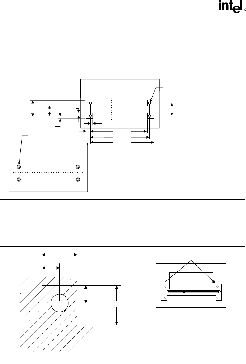
Layout/Routing Guidelines
2-48 Intel®820 Chipset Design Guide
Motherboard Interfaces
Figure 2-39 shows the Hole Locations and Keepout Zones For Support Components (from the
motherboard surface to 0.100” above the motherboard surface.).
NOTES:
1. The dashed lines represent the centerlines for the connector keying features.
2. Drawing not to scale
Figure 2-40 shows the dimensions of the grounding pad needed to ground the heat sink.
NOTE: Drawing not to scale.
It is not recommended to use the GRM without the minimum size ground pads in the correct
locations. If the GRM is used without the correct pads, then there is a high risk that the metal clip
that grounds to the motherboard will be touching the solder mask on the top layer of the board, and
possibly short out traces immediately beneath the solder mask, resulting in board failure. The
required thickness of the pad is less than 0.001” (using 1/2 oz. copper).
Figure 2-39. Hole Locations and Keepout Zones For Support Components1,2
1.270 0.806 0.232
0.231 0.375
4x ∅ 0.300 Keepout
Secondary Side
Primary Side
4.706
4.881
4x Thru ∅ 0.159 +0.002
-0.001
1.038
1. All dimensions are in inches and all tolerances ±0.04, unless
otherwise specified.
2. Dash lines represent control line for connector key features when
placed on planar.
3. Retention solution not to exceed height of 2.75" off of primary
side of planar and 0.150" off of secondary side of planar.
4. Retention mechanism must stay within cross-hatch area.
0.175
5.256
Figure 2-40. Grounding Pad Dimensions for the SECC2 GRM
0.182
Ground Pad Areas,
See Detail A
Notes:
1. All dimensions are in inches and all
tolerances are ±0.004, unless otherwise
specified.
2. Retention mechanisim must stay within
Cross-Hatch area.
3. Entire specified plating area must be plated
and grounded with a minimum of eight VIAS.
Heat Sink Area
0.364
0.464
0.232
Detail A

Intel®820 Chipset Design Guide 2-49
Layout/Routing Guidelines
2.11 Processor CMOS Pullup Values
Table 2-13 contains the pullup values for the Intel® Pentium® III processor with the Intel® 820
chipset. This table supports both single and dual processor configurations.
Table 2-13. Processor and 82820 MCH Connection Checklist1,2
CPU Pin UP Pin Connection (CPU0) DP Pin Connection (CPU1)
AGTL+ Signals
A[35:3]# 1Connect A[31:3]# to MCH. Leave A[35:32]#
as N/C (not supported by chipset). Connect A[31:3]# to 2nd processor
ADS# 1Connect to MCH Connect to 2nd processor
AERR# Leave as N/C (not supported by chipset). Leave as N/C
AP[1:0]# Leave as N/C (not supported by chipset). Leave as N/C
BERR# Leave as N/C (not supported by chipset). Leave as N/C
BINIT# Leave as N/C (not supported by chipset). Leave as N/C
BNR# 1Connect to MCH Connect to 2nd processor
BP[3:2]# Leave as N/C Leave as N/C
BPM[1:0] Leave as N/C Leave as N/C
BPRI# 1Connect to MCH Connect to 2nd processor
BREQ0# (BR0#) 10 Ω pull down to GND See and
BREQ1# (BR1#) Leave as N/C See and
D[63:0]# 1Connect to MCH Connect to 2nd processor
DBSY# 1Connect to MCH Connect to 2nd processor
DEFER# 1Connect to MCH Connect to 2nd processor
DEP[7:0]# Leave as N/C (not supported by chipset). Leave as N/C
DRDY# 1Connect to MCH Connect to 2nd processor
HIT# 1Connect to MCH Connect to 2nd processor
HITM# 1Connect to MCH Connect to 2nd processor
LOCK# 1Connect to MCH Connect to 2nd processor
REQ[4:0]# 1Connect to MCH Connect to 2nd processor
RESET# 1Connect to MCH, 240 Ω series resistor to ITP Connect to 2nd processor
RP# Leave as N/C (not supported by chipset). Leave as N/C
RS[2:0]# 1Connect to MCH Connect to 2nd processor
RSP# Leave as N/C (not supported by chipset). Leave as N/C
TRDY# 1Connect to MCH Connect to 2nd processor
Layout/Routing Guidelines
2-50 Intel®820 Chipset Design Guide
CMOS Signals
A20M# 150 Ω pull up to Vcc2.5, connect to ICH Connect to 2nd processor
FERR# 150 Ω pull up to Vcc2.5, connect to ICH Connect to 2nd processor
FLUSH# 150 Ω pull up to Vcc2.5 (not used by chipset). Connect to 2nd processor
IERR# 150 Ω pull up to Vcc2.5 if tied to custom logic
or leave as N/C (not used by chipset). Connect to 2nd processor
IGNNE# 150 Ω pull up to Vcc2.5, connect to ICH Connect to 2nd processor
INIT# 150 Ω pull up to Vcc2.5, connect to ICH and
FWH Flash BIOS Connect to 2nd processor
LINT0/INTR 150 Ω pull up to Vcc2.5, connect to ICH Connect to 2nd processor
LINT1/NMI 150 Ω pull up to Vcc2.5, connect to ICH Connect to 2nd processor
PICD[1:0] 150 Ω pull up to Vcc2.5, connect to ICH Two 300–330 Ω pull ups to Vcc2.5 located
at each end of trace. Connect to 2nd
processor
PREQ# ~200–330 Ω pull up to Vcc2.5, connect to ITP
pin 16 ~200–330 Ω pull up to Vcc2.5, connect to
ITP pin 20
PWRGOOD 150–330 Ω pull up to 2.5V, output from the
PWRGOOD logic Connect to 2nd processor
SLP# 150 Ω pull up to Vcc2.5, connect to ICH
SMI# 150 Ω pull up to Vcc2.5, connect to ICH
STPCLK# 150 Ω pull up to Vcc2.5, connect to ICH
THERMTRIP# 150 Ω pull up to Vcc2.5 and connect to power
off logic or ASIC, or leave as N/C Connect to 2nd processor. Could tie
separately to a monitoring ASIC.
TAP Signals
PRDY# 150 Ω pull up to VTT, 240 Ω series resistor to
ITP pin 18 150 Ω pull up to VTT, 240 Ω series resistor
to ITP pin 22
TCK 1k Ω pull up to Vcc2.5, 47 Ω series resistor to
ITP pin 5
Each processor should receive a
separately buffered copy of TCK from the
ITP. Tank circuit is optional for signal
integrity. See
TDO 150 Ω pull up to Vcc2.5 and connect to ITP
10
TDO of CPU1 is connected to the ITP TDO
pin 10. Pull up both sets of TDI/TDO nets
as described.
TDI ~150–330 Ω pull up to Vcc2.5 and connect to
ITP pin 8
TDI of CPU0 is connected to the ITP pin 8,
TDI of CPU1 is connected to TDO of
CPU0. Pull up both sets of TDI/TDO nets
as described.
TMS 1KΩ pull up to Vcc2.5, 47 Ω series resistor
to ITP pin 7
Each processor should receive a
separately buffered copy of TMS from the
ITP.
Tank circuit is optional for signal integrity.
See
TRST# ~680 Ω pull down, connect to ITP pin 12 Connect to 2nd processor
Table 2-13. Processor and 82820 MCH Connection Checklist1,2 (Continued)
CPU Pin UP Pin Connection (CPU0) DP Pin Connection (CPU1)
Intel®820 Chipset Design Guide 2-51
Layout/Routing Guidelines
NOTES:
1. For single processor designs, the AGTL+ bus can be dual-ended or single-ended termination based on
simulation results. Single-ended termination is provided by the processor.
2. This checklist supports Intel® Pentium® II processors at all current speeds, Intel® Pentium® III processors to
a FMB guideline of 19.3A, and future Intel® Pentium® III processors to the current FMB guideline of 18.4A.
Clock Signals
BCLK
Connect to CK133. 22 – 33 Ω series resistor
(Though OEM needs to simulate based on
driver characteristics). To reduce pin-to-pin
skew, tie host clock outputs together at the
clock driver then route to the MCH and
processor.
Use separate BCLK from TAP and CPU0,
or use ganged clock. Terminate as
described.
PICCLK Connect to CK133. 22 – 33 Ω series resistor
(Though OEM needs to simulate based on
driver characteristics)
Use separate PICCLK from CPU0.
Terminate as described.
Other Signals
BSEL0 100/133 MHz support: 220 Ω pull up to 3.3V,
connected to PWRGOOD logic such that a
logic low on BSEL0 negates PWRGOOD Connect to 2nd processor
BSEL1 220 Ω pull up to 3.3V, connect to CK133
SEL133/100# pin. Connect to MCH HL10 pin
via 8.2 KΩ series resistor. Connect to 2nd processor
EMI[5:1] Tie to GND. Zero ohm resistors are an option
instead of direct connection to GND. Implement in same manner as CPU0.
SLOTOCC#
Tie to GND, leave it N/C, or could be
connected to powergood logic to gate system
from powering on if no processor is present.
If used, 1 KΩ – 10 KΩ pull up to any voltage.
Implement in same manner as CPU0.
TESTHI
1K–100KΩ pull up to Vcc2.5
If a legacy design pulls this up to VCCCORE,
use a 1 KΩ – 10 KΩ pull up
Implement in same manner as CPU0.
VID[4:0]
Connect to on-board VR or VRM. For on-
board VR, 10 KΩ pull up to power-solution
compatible voltage required (usually pulled
up to input voltage of the VR). Some of these
solutions have internal pull-ups. Optional
override (jumpers, ASIC, etc.) could be used.
May also connect to system monitoring
device.
Implement in same manner as CPU0.
CPU0 and CPU1 should have different
VR/VRMs.
Power
VCCCORE Connect to core voltage regulator. Provide
high & low frequency decoupling. Implement in same manner as CPU0.
VTT Connect to 1.5V regulator. Provide high and
low frequency decoupling. Implement in same manner as CPU0.
No Connects
Reserved The following pins must be left as no-
connects: A16, A47, A88, A113, A116, B12,
B20, B76, and B112. Implement in same manner as CPU0.
Table 2-13. Processor and 82820 MCH Connection Checklist1,2 (Continued)
CPU Pin UP Pin Connection (CPU0) DP Pin Connection (CPU1)
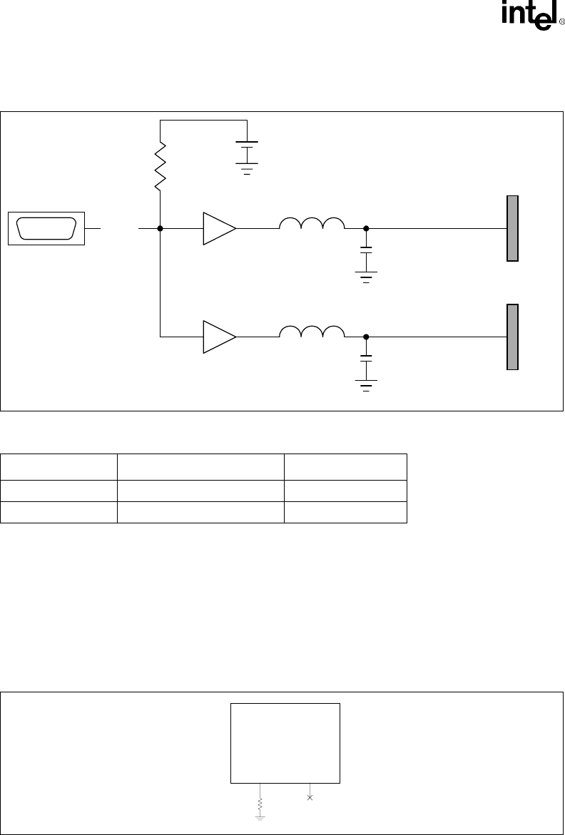
Layout/Routing Guidelines
2-52 Intel®820 Chipset Design Guide
2.12 Additional Host Bus Guidelines
BREQ Pins
UP Systems: For uni-processor systems, the BREQ0 pin should be pulled down to ground through
a 10 Ω resistor. The BREQ1 pin should be left as a no-connect.
Figure 2-41. TCK/TMS Implementation Example for DP Designs
Table 2-14. Bus Request Connection Scheme for DP Intel® 820 Chipset Designs
Bus Signal Agent 0 Pins Agent 1 Pins
BREQ0# BR0# BR1#
BREQ1# BR1# BR0#
TCK
or
TMS
ITP Port
Vcc2.5
1 K
Ω
R
I
100 nH
100 nH
56 pF
56 pF
SC242
Connector A
SC242
Connector B
itp vsd
non-inverting buffer
non-inverting buffer
motherboard trace
motherboard trace
Figure 2-42. Single Processor BREQ Strapping Requirements
CPU #1
BREQ0# BREQ1#
No Connect
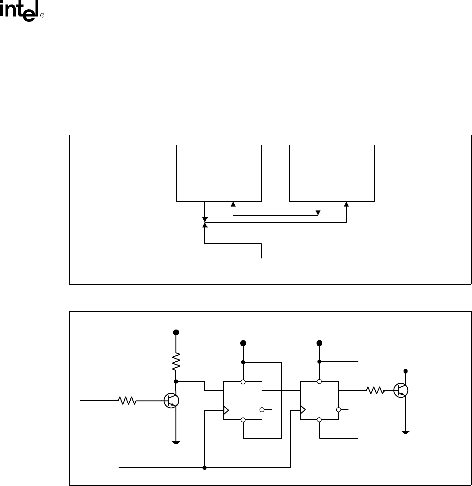
Intel®820 Chipset Design Guide 2-53
Layout/Routing Guidelines
DP Systems: For dual processor systems, BREQ0# (to one of the processors) needs to be driven
for arbitration ID strapping. Refer to Figure 2-43 for an example of the BREQ connections in a DP
system. It is a requirement that the on-board logic tri-state BREQ0# after the arbitration ID
strapping is complete. Additionally, BREQ0# and BREQ1# are high-speed AGTL+ signals and the
loading characteristics of the on-board logic must be considered even when the logic is tri-stated.
This circuit holds BREQ0 low for two clocks after the deassertion of reset. The 2N3904 connected
to BREQ0 should be connected to the BREQ0 AGTL trace with a very short stub. Additionally, the
series current limiting resistor on CPURESET should be attached to the CPURESET trace with a
very short stub.
External Circuit Recommendation for HA7 Strapping for IOQ Depth of 1
For debug purpose, the external logic to set the IOQ depth of 1 on the front side bus may be
needed. Do not add this circuit for production since overall system performance will be degraded.
The external logic for HA7# strapping is very similar to the BREQ0 strapping that is described in
the previous section.
The timing requirement of HA7# strapping is also similar to BREQ0 strapping for the hold time
after the deassertion of RESET# (RSTIN# signal from MCH). The value of the strapping needs to
be held for a minimum of 2 host clocks after the deassertion of RSTIN#. Refer to the latest version
of the processor datasheets for complete description on the timing requirement.
Figure 2-43. Dual-Processor BREQ Strapping Requirements
Figure 2-44. BREQ0# Circuitry for DP Systems
CPU #1 CPU #2
BREQ0# BREQ0# BREQ1#BREQ1#
on-board logic
CPURST#
CPUCLK
R2
2.7 K
Ω
ΩΩ
Ω
5V
5V5V
25
6
4
1
3
1
2
3
4
5
6
QQ
/Q /Q
D/PRE
/CLR
/PRE
/CLR
D
CLK CLK
74F74 74F74
2N3904
2N3904
BREQ0#
R2
4.7 K
Ω
ΩΩ
Ω
4.7 K
Ω
ΩΩ
Ω

Layout/Routing Guidelines
2-54 Intel®820 Chipset Design Guide
The recommendation for the layout and the schematic example are shown below. Layout
guidelines are:
•Place the transistor and stub as close as possible to MCH (or place the transistor pad on top of
trace)
•The max stub for transistor is less than 0.25”
•The recommended loading of transistor is less than 5 pf.
•For dual processor design, the stub is recommended to place on the stub of the MCH and as
close as possible to the MCH, and is less than 0.25”
Note: This circuit is only recommended for the debug situation that requires to set the IOQ depth equal to
1. For the production, do not add this circuit, since the overall system performance will be
degraded. Also, Intel does not guarantee the above layout recommendation will work under the
worst case condition.
In-Target Probe (ITP)
It is important that all of the processor electrical characteristic requirements are met. It is
recommended that prototype boards implement the ITP connector.
Logic Analyzer Interface (LAI)
Note that 1 KΩ resistors that are used to pull-up several processor signals in the schematics in
Appendix A, “Reference Design Schematics: Uni-Processor” and Appendix B, “Reference Design
Schematics: Dual-Processor” (e.g., HINIT#, IGNNE#, SMI#, etc.) preclude use of the Intel
Pentium III processor LAI. The Intel Pentium III processor LAI will function correctly with these
1KΩ pull-up resistors.
Figure 2-45. HA7# Strapping Option Example Circuit (For Debug Purposes Only)
CPURST#
CPUCLK
R2
2.7 K
Ω
ΩΩ
Ω
5V
5V5V
25
6
4
1
3
1
2
3
4
5
6
QQ
/Q /Q
D/PRE
/CLR
/PRE
/CLR
D
CLK CLK
74F74 74F74
2N3904
2N3904
HA7
R2
4.7 K
Ω
ΩΩ
Ω
R2
4.7 K
Ω
ΩΩ
Ω
jumper
4.7 K
Ω
ΩΩ
Ω

Intel®820 Chipset Design Guide 2-55
Layout/Routing Guidelines
Minimizing Crosstalk on the AGTL+ Interface
The following general rules will minimize the impact of crosstalk in the high speed AGTL+ bus
design:
•Maximize the space between traces. Maintain a minimum of 0.010” between traces wherever
possible. It may be necessary to use tighter spacings when routing between component pins.
•Avoid parallelism between signals on adjacent layers.
•Since AGTL+ is a low signal swing technology, it is important to isolate AGTL+ signals from
other signals by at least 0.025”. This will avoid coupling from signals that have larger voltage
swings, such as 5V PCI.
•Select a board stack-up that minimizes the coupling between adjacent signals.
•Route AGTL+ address, data and control signals in separate groups to minimize crosstalk
between groups. The Pentium III processor uses a split transaction bus. In a given clock cycle,
the address lines and corresponding control lines could be driven by a different agent than the
data lines and their corresponding control lines.
Additional Considerations
•Distribute VTT with a wide trace. A 0.050” minimum trace is recommended to minimize DC
losses. Route the VTT trace to all components on the host bus. Be sure to include decoupling
capacitors. Guidelines for VTT distribution and decoupling are contained in “Slot 1 Processor
Power Distribution Guidelines.”
•Place resistor divider pairs for VREF generation at the MCH component. No VREF generation
is needed at the processor(s). VREF is generated locally on the processor. Be sure to include
decoupling capacitors. Guidelines for VREF distribution and decoupling are contained in “Slot
1 Processor Power Distribution Guidelines.”
•Special Case AGTL+ signals for simulation: There are six AGTL+ signals that can be driven
by more than one agent simultaneously. These signals may require extra attention during the
layout and validation portions of the design. When a signal is asserted (driven low) by two
agents on the same clock edge, the two falling wave fronts will meet at some point on the bus.
This can create a large undershoot, followed by ringback which may violate the ringback
specifications. This “wired-OR” situation should be simulated for the following signals:
AERR#, BERR#, BINIT#, BNR#, HIT#, and HITM#.

Layout/Routing Guidelines
2-56 Intel®820 Chipset Design Guide
2.13 Ultra ATA/66
This section contains guidelines for connecting and routing the ICH IDE interface. The ICH has
two independent IDE channels. This section provides guidelines for IDE connector cabling and
motherboard design, including component and resistor placement, and signal termination for both
IDE channels. The ICH has integrated the 33 Ω series resistors that have been typically required on
the IDE data signals running to the two ATA connectors.
The IDE interface can be routed with 5 mil traces on 5 mil spaces, and must be less than 8 inches
long (from ICH to IDE connector). Additionally, the shortest IDE signal (on a given IDE channel)
must be less than 0.5” shorter than the longest IDE signal (on that channel).
Cable
•Length of cable: Each IDE cable must be equal to or less than 18 inches.
•Capacitance: Less than 30 pF.
•Placement: A maximum of 6 inches between drive connectors on the cable. If a single drive is
placed on the cable it should be placed at the end of the cable. If a second drive is placed on the
same cable it should be placed on the next closest connector to the end of the cable (6” away
from the end of the cable).
•Grounding: Provide a direct low impedance chassis path between the motherboard ground
and hard disk drives.
•ICH Placement: The ICH must be placed equal to or less than 8 inches from the ATA
connector(s).
•PC99 requirement: Support Cable Select for master-slave configuration is a system design
requirement for Microsoft* PC99. CSEL signal needs to be pulled down at the host side by
using a 470 Ω pull-down resistor for each ATA connector.
2.13.1 Ultra ATA/66 Detection
The Intel® 820 chipset supports many Ultra DMA modes including ATA/66. The Intel® 820
chipset needs to determine the installed IDE device mode and the type of cable to configure its own
hardware and software to support it.
A new IDE cable is required for Ultra ATA/66. This cable is an 80 conductor cable; however the 40
pin connectors do not change. The wires in the cable alternate: ground, signal, ground, signal,
ground, signal, ground… All the ground wires are tied together on the cable (and they are tied to
the ground on the motherboard through the ground pins in the 40 pin connector). This cable
conforms to the Small Form Factor Specification SFF-8049. This specification can be obtained
from the Small Form Factor Committee.
To determine if ATA/66 mode can be enabled, the Intel® 820 chipset requires the system BIOS to
attempt to determine the cable type used in the system. The BIOS does this in one of two ways:
•Host Side Detection
•Device Side Detection
If the BIOS detects an 80-conductor cable, it may use any Ultra DMA mode up to the highest
transfer mode supported by both the Intel® 820 chipset and the IDE device. Otherwise, the BIOS
can only enable modes that do not require an 80-conductor cable (e.g., Ultra ATA/33 Mode).
After determining the Ultra DMA mode to be used, the BIOS will configure the Intel® 820 chipset
hardware and software to match the selected mode.
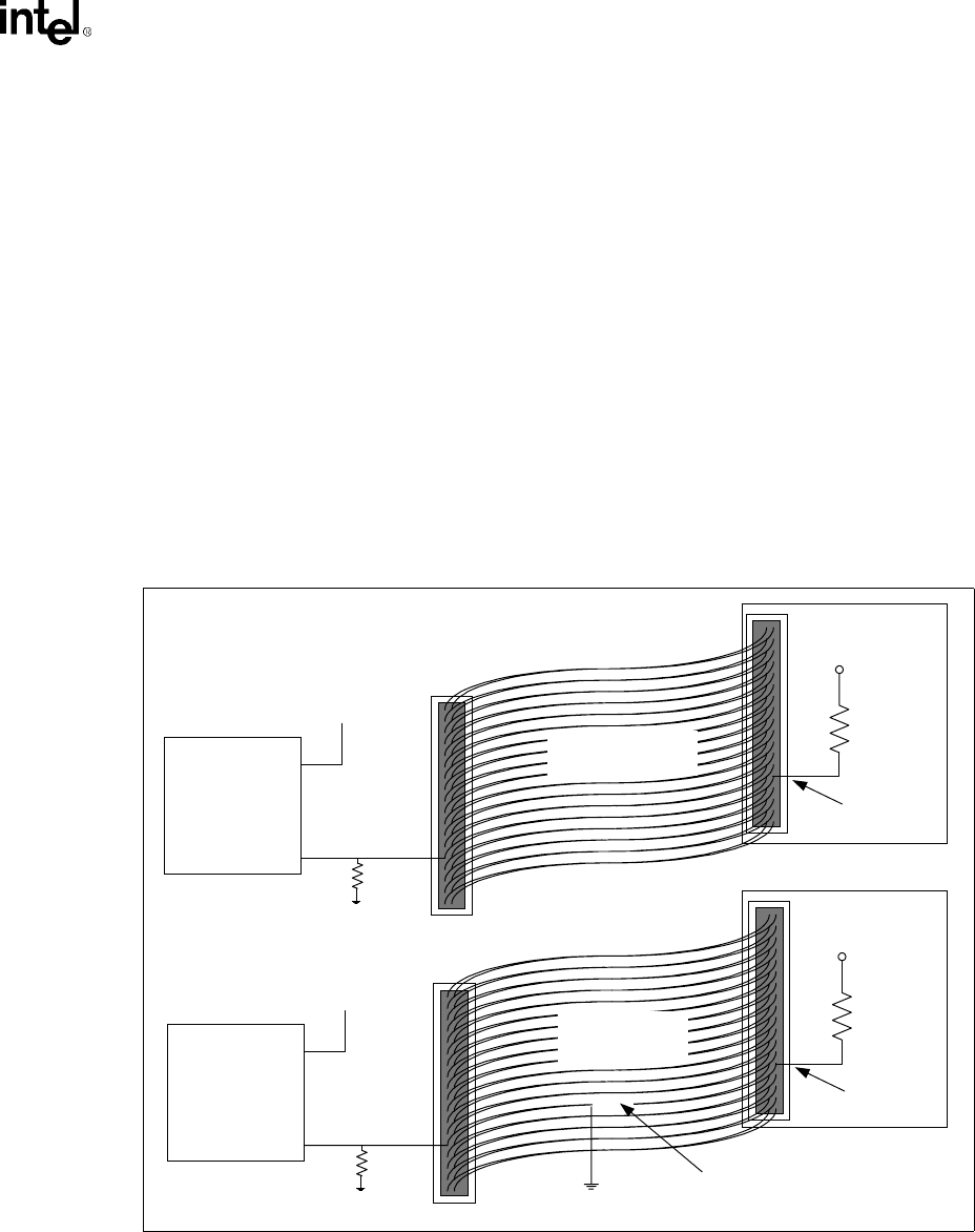
Intel®820 Chipset Design Guide 2-57
Layout/Routing Guidelines
2.13.2 Ultra ATA/66 Cable Detection
The Intel® 820 chipset can use two methods to detect the cable type. Each mode requires a
different motherboard layout.
Host-Side Detection (BIOS Detects Cable Type Using GPIOs)
Host side detection requires the use of two GPI pins (1 per IDE controller). The proper way to
connect the PDIAG/CBLID signal of the IDE connector to the host is shown in Figure 2-46. All
IDE devices have a 10 KΩ pull-up resistor to 5 volts. The GPI and GPIO pins on the ICH and GPI
pins on the FWH Flash BIOS are not 5 volt tolerant. This requires a resistor divider so that 5 volts
will not be driven to the ICH or FWH Flash BIOS pins. The proper value of the series resistor is
15 KΩ (as shown in Figure 2-46). This creates a 10 KΩ / 15 KΩ resistor divider and produces
approximately 3 volts for a logic high.
This mechanism allows the host, after diagnostics, to sample PDIAG/CBLID. If PDIAG/CBLIB is
high then there is 40-conductor cable in the system and ATA modes 3 and 4 should not be enabled.
If PDIAG/CBLID is low then there is an 80-conductor cable in the system.
Figure 2-46. Host-Side IDE Cable Detection
80-Conductor
IDE Cable
IDE Drive
10 K
Ω
5V
PDIAG
ICH
GPIO
GPIO
To Secondary
IDE Connector
Open
15 K
Ω
40-Conductor
Cable
IDE Drive
10 K
Ω
5V
PDIAG
ICH
GPIO
GPIO
To Secondary
IDE Connector
15 K
Ω
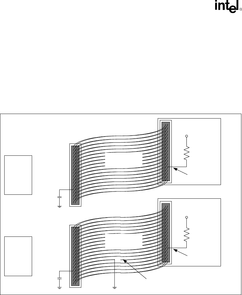
Layout/Routing Guidelines
2-58 Intel®820 Chipset Design Guide
Device-Side Detection (BIOS Queries IDE Drive for Cable Type)
Device side detection requires only a 0.047 uF capacitor on the motherboard as shown in
Figure 2-47. This mechanism creates a resistor-capacitor (RC) time constant. The ATA mode 3 or 4
drive will drive PDIAG/CBLID low and then release it (pulled up through a 10 KΩ resistor) The
drive will sample the PDIAG signal after releasing it. In an 80-conductor cable, PDIAG/CBLID is
not connected through and, therefore, the capacitor has no effect. In a 40-conductor cable, PDIAG/
CBLID is connected though to the drive. Therefore, the signal rises more slowly. The drive can
detect the difference in rise times and it reports the cable type to the BIOS when it sends the
IDENTIFY_DEVICE packet during system boot as described in the ATA/66 specification.
Layout for BOTH Host-Side and Drive-Side Cable Detection
It is possible to layout for both Host-Side and Drive-Side cable detection and decide the method to
be used during assembly. Figure 2-48 shows the layout that allows for both host-side and drive-side
detection.
•For Host-Side Detection:
—R1 is a 0Ω resistor
—R2 is a 15KΩ resistor
— C1 is not stuffed
•For Drive-Side Detection:
— R1 is not stuffed
— R2 is not stuffed
— C1 is a 0.047 uF capacitor
Figure 2-47. Drive-Side IDE Cable Detection
40-Conductor
Cable
IDE Drive
10 K
Ω
5V
PDIAG
ICH
0.047 uF
IDE Drive
10 K
Ω
5V
PDIAG
ICH
Open
0.047 uF
80-Conductor
IDE Cable
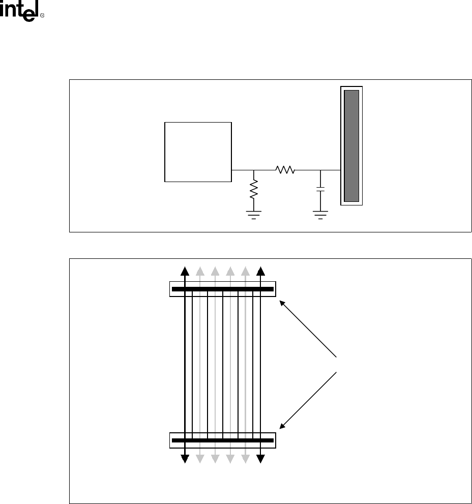
Intel®820 Chipset Design Guide 2-59
Layout/Routing Guidelines
Figure 2-48. Layout for Host- or Drive-Side IDE Cable Detection
Figure 2-49. Ultra ATA/66 Cable
ICH
C1
R1
R2
id 1 d
IDE Connector
Black wires are ground
Grey wires are signals
Layout/Routing Guidelines
2-60 Intel®820 Chipset Design Guide
2.13.3 Ultra ATA/66 Pullup/Pulldown Requirements
•22 Ω – 47 Ω series resistors are required on RESET#. The correct value should be determined
for each unique motherboard design, based on signal quality.
•An 8.2 KΩ to 10 KΩ pull-up resistor is required on IRQ14 and IRQ15 to VCC5.
•A 10 KΩ pull-down resistor is required on PDD7 and SDD7 (as required by the ATA-4
specification).
•A 5.6 KΩ pull-down resistor is required on PDDREQ# and SDDREQ# (as required by the
ATA-4 specification).
•A 1K Ω pull-up resistor is required on PIORDY and SIORDY (as required by the ATA-4
specification).
Figure 2-50. Resistor Requirements for Primary IDE Connector
5.6k
ohm
Reset#
Primary IDE Connector
ICH
10k
ohm
PDD[15:8]
PDD[6:0]
PCIRST_BUF#*
22 - 47 ohm
PDA[2:0]
PDCS1#
PDCS3#
PDIOR#
PDIOW#
PDDREQ
PIORDY
PDD[7]
*Due to ringing, PCIRST# must be buffered.
1k
ohm
5V
470 ohm
CSEL
Pin 34
N.C.
PDDACK#
IRQ14
5V
8.2k-10k
ohm
Pin 32
N.C.
Intel®820 Chipset Design Guide 2-61
Layout/Routing Guidelines
2.14 AC’97
The ICH implements an AC’97 2.1 compliant digital controller. Any codec attached to the ICH
AC-link must be AC’97 2.1 compliant as well. Contact your codec IHV for information on 2.1
compliant products. The AC’97 2.1 specification is on the Intel website. The ICH supports the
following combinations of codecs:
As shown in the table, the ICH does not support two codecs of the same type on the link. For
example, if an AMC is on the link, it must be the only codec. If an AC is on the link, another AC
cannot be present.
Intel has developed a common connector specification known as the Audio/Modem Riser (AMR).
This specification defines a mechanism for allowing OEM plug-in card options.
Figure 2-51. Resistor Requirements for Secondary IDE Connector
5.6k
ohm
Reset#
Secondary IDE Connector
ICH
10k
ohm
SDD[15:8]
SDD[6:0]
PCIRST_BUF#*
22 - 47 ohm
SDA[2:0]
SDCS1#
SDCS3#
SDIOR#
SDIOW#
SDDREQ
SIORDY
SDD[7]
*Due to ringing, PCIRST# must be buffered.
1k
ohm
5V
470 ohm CSEL
Pin 32
N.C.
SDDACK#
IRQ15
5V
8.2k-10k
ohm
Pin 34
N.C.
Table 2-15. ICH Codec Options
Primary Secondary
Audio (AC) None
Modem (MC) None
Audio (AC) Modem (MC)
Audio/Modem (AMC) None
Layout/Routing Guidelines
2-62 Intel®820 Chipset Design Guide
The AMR specification provides a mechanism for AC’97 codecs to be on a riser card. This is
important for modem codecs as it helps ease international certification of the modem.
For increased part placement flexibility, there are two routing methods for the AC’97 interface: the
tee topology and the daisy-chain topology. The AC’97 interface can be routed using 5 mil traces
with 5 mil space between the traces.
Figure 2-52. Tee Topology AC'97 Trace Length Requirements
Figure 2-53. Daisy-Chain Topology AC'97 Trace Length Requirements
ICH
Codec
A
M
R
4" Max
2" Max 3" Max
ICH Codec
A
M
R
5" Max 3" Max
Intel®820 Chipset Design Guide 2-63
Layout/Routing Guidelines
Clocking is provided from the primary codec on the link via BITCLK, and is derived from a
24.576 MHz crystal or oscillator. Refer to the primary codec vendor for crystal or oscillator
requirements. BITCLK is a 12.288 MHz clock driven by the primary codec to the digital controller
(ICH), and any other codec present. That clock is used as the timebase for latching and driving
data.
On the Intel® 820 chipset platform, the ICH supports Wake on Ring from S1, S3, and S4 via the
AC’97 link. The codec asserts SDATAIN to wake the system. To provide wake capability and/or
caller ID, standby power must be provided to the modem codec.
The ICH has weak pulldowns/pullups that are only enabled when the AC-Link Shut Off bit in the
ICH is set. This will keep the link from floating when the AC-link is off, or there are no codecs
present.
If the Shut-off bit is not set, it implies that there is a codec on the link. Therefore, BITCLK and
AC_SDOUT will be driven by the codec and ICH respectively. However, AC_SDIN0 and
AC_SDIN1 may not be driven. If the link is enabled, the assumption can be made that there is at
least one codec. If there is an onboard codec only (i.e., no AMR), then the unused SDIN pin should
have a weak (10 KΩ) pulldown to keep it from floating. If an AMR is used, any SDIN signal that
could be no connected (e.g., with no codec, both can be NC), then both SDIN pins must have a
10 KΩ pulldown.
NOTE: If the on-board codec can be disabled, both SDIN pins must have pulldowns. If the on-board codec can
not be disabled, only the SDIN not connected to the on-board codec requires a pulldown.
2.14.1 AC’97 Signal Quality Requirements
In a lightly loaded system (e.g., single codec down), AC'97 signal integrity should be evaluated to
confirm that the signal quality on the link is acceptable to the codec used in the design. A series
resistor at the driver and a capacitor at the codec can be implemented in order to compensate for
any signal integrity issues. The values used will be design dependent and should be verified for
correct timings. The ICH AC-link output buffers are designed to meet the AC'97 2.1 specification
with the specified load of 50pF.
2.14.2 AC’97 Motherboard Implementation
The following design considerations are provided for the implementation of an ICH0/ICH platform
using AC’97. These design guidelines have been developed to ensure maximum flexibility for
board designers while reducing the risk of board related issues. These recommendations do not
represent the only implementation or a complete checklist, but provides recommendations based on
the ICH0/ICH platform.
Table 2-16. AC'97 SDIN Pulldown Resistors
System Solution Pullup Requirements
On-board Codec Only Pulldown the SDIN pin that is NOT connected to the codec
AMR Only Pulldown BOTH SDIN pins
BOTH AMR and On-board Codec Pulldown any SDIN pin that could be NC*

Layout/Routing Guidelines
2-64 Intel®820 Chipset Design Guide
•Codec Implementation
— The motherboard can implement any valid combination of codecs on the motherboard and
on the riser. For ease of homologation, it is recommended that a modem codec be
implemented on the AMR module; however, nothing precludes a modem codec on the
motherboard.
— Only one primary codec can be present on the link. A maximum of two present codecs can
be supported in an ICH0/ICH platform.
— If the motherboard implements an active primary codec on the motherboard and provides
an AMR connector, it must tie PRI_DN# to ground.
— The PRI_DN# pin is provided to indicate a primary codec is present on the motherboard.
Therefore, the AMR module and/or codec must provide a means to prevent contention
when this signal is asserted by the motherboard, without software intervention.
— Components (e.g., FET switches), buffers, or logic states should not be implemented on
the AC-link signals, except for AC_RST#. Doing so will potentially interfere with timing
margins and signal integrity.
— If the motherboard requires that an AMR module override a primary codec down, a means
of preventing contention on the AC-link must be provided for the onboard codec.
— The ICH0/ICH supports Wake on Ring* from S1-S4 states via the AC’97 link. The codec
asserts SDATAIN to wake the system. To provide wake capability and/or caller ID,
standby power must be provided to the modem codec. If no codec is attached to the link,
internal pulldowns will prevent the inputs from floating, therefore external resistors are
not required. The ICH0/ICH does not wake from the S5 state via the AC’97 link.
— The SDATAIN[0:1] pins should not be left in a floating state if the pins are not connected
and the AC-link is active—they should be pulled to ground through a weak
(approximately 10 KΩ) pull-down resistor. If the AC-link is disabled (by setting the shut-
off bit to 1), then the ICH0/ICH’s internal pull-down resistors are enabled, and thus there
is no need for external pull-down resistors. However, if the AC-link is to be active, then
there should be pull-down resistors on any SDATAIN signal that has the potential of not
being connected to a codec. For example, if a dedicated audio codec is on the
motherboard, and cannot be disabled via a hardware jumper or stuffing option, then its
SDATAIN signal does not need a pull-down resistor. If however, the SDATAIN signal has
no codec connected, or is connected to an AMR slot, or is connected to an onboard codec
that can be hardware disabled, then the signal should have an external pull-down resistor
to ground.
•AMR Slot Special Connections
— AUDIO_MUTE#: No connect on the motherboard.
— AUDIO_PWRDN: No connect on the motherboard. Codecs on the AMR card should
implement a powerdown pin, per the AC’97 2.1 specification, to control the amplifier.
— MONO_PHONE: Connect top onboard audio codec if supported.
— MONO_OUT/PC_BEEP: Connect to SPKR output from the ICH0/ICH, or MONO_OUT
from onboard codec.
— PRIMARY_DN#: See discussion above.
— +5VDUAL/+5VSB: Connect to VCC5 core on the motherboard, unless adequate power
supply is available. An AMR card using this standby/dual supply should not prevent basic
operation if this pin is connected to core power.
— S/P-DIF_IN: Connect to ground on the motherboard.
— AC_SDATAIN[3:2]: No connect on the motherboard. The ICH0/ICH supports a
maximum of two codecs, which should be attached to SDATAIN[1:0].
— AC97_MSTRCLK: Connect to ground on the motherboard.
•The ICH0/ICH provides internal weak pulldowns. Therefore, the motherboard does not need
to provide discrete pulldown resistors.
•PC_BEEP should be routed through the audio codec. Care should be taken to avoid the
introduction of a pop when powering the mixer up or down.
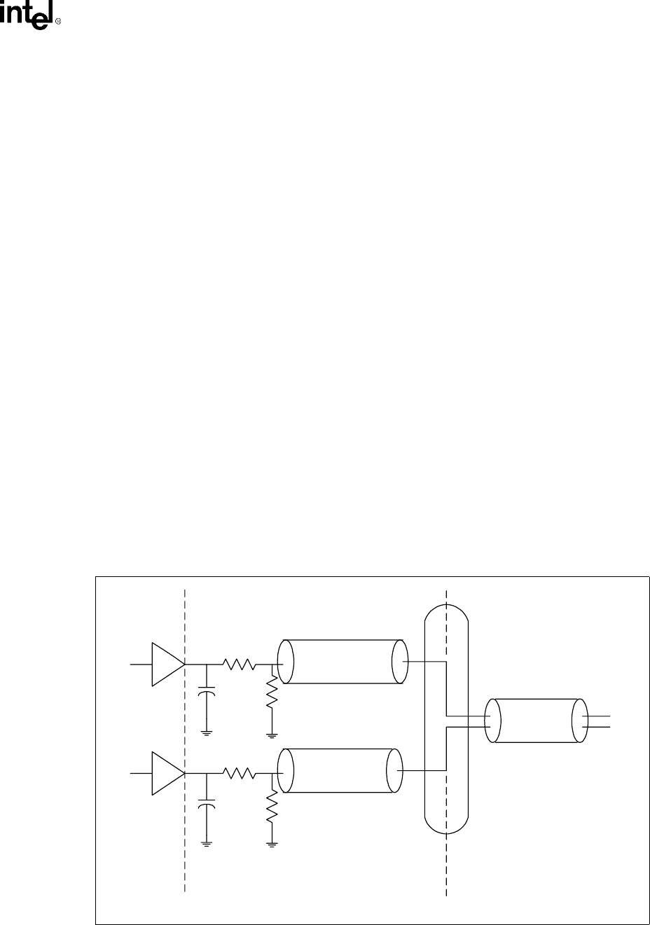
Intel®820 Chipset Design Guide 2-65
Layout/Routing Guidelines
2.15 USB
The following are general guidelines for the USB interface:
•Unused USB ports should be terminated with 15 KΩ pulldown resistors on both P+/P- data
lines.
•15 Ω series resistors should be placed as close as possible to the ICH (<1 inch). These series
resistors are required for source termination of the reflected signal.
•47 pF caps must be placed as close to the ICH as possible and on the ICH side of the series
resistors on the USB data lines (P0+/-, P1+/-). These caps are there for signal quality (rise/fall
time) and to help minimize EMI radiation.
•15 KΩ ±5% pulldown resistors should be placed on the USB side of the series resistors on the
USB data lines (P0+/-, P1+/-), and are REQUIRED for signal termination by USB
specification. The length of the stub should be as short as possible.
•The trace impedance for the P0+/-, P1+/- signals should be 45 Ω (to ground) for each USB
signal P+ or P-. Using the stackup recommended in section Section 5.3, “Stackup
Requirement” on page 5-1. USB requires 9 mils traces. The impedance is 90 Ω between the
differential signal pairs P+ and P- to match the 90 Ω USB twisted pair cable impedance. Note
that twisted pair characteristic impedance of 90 Ω is the series impedance of both wires,
resulting in an individual wire presenting a 45 Ω impedance. The trace impedance can be
controlled by carefully selecting the trace width, trace distance from power or ground planes,
and physical proximity of nearby traces.
•USB data lines must be routed as critical signals. The P+/P- signal pair must be routed together
and not parallel with other signal traces to minimize crosstalk. Doubling the space from the
P+/P- signal pair to adjacent signal traces will help to prevent crosstalk. Do not worry about
crosstalk between the two P+/P- signal traces. The P+/P- signal traces must also be the same
length. This will minimize the effect of common mode current on EMI.
Figure 2-54 illustrates the recommended USB schematic.
Figure 2-54. USB Data Signals
15k
15k
15 ohm
15 ohm
47 pf
47 pf
ICH
P+
P-
USB Connector
< 1"
< 1"
90 ohm
45 ohm
45 ohm
Driver
Driver
USB Twisted Pair CableTransmission Line
Motherboard Trace
Motherboard Trace

Layout/Routing Guidelines
2-66 Intel®820 Chipset Design Guide
Recommended USB trace characteristics
•Impedance ‘Z0’ = 45.4 Ω
•Line Delay = 160.2 ps
•Capacitance = 3.5 pF
•Inductance = 7.3 nH
•Res @ 20° C = 53.9 mOhm
2.16 ISA (82380AB)
2.16.1 ICH GPIO connected to 82380AB
At reset, the ICH LPC Bridge defaults to subtractive decode. Since the LPC bridge logically sits on
PCI there will be two subtractive decode bridges in systems with the 82380AB (which is also a
subtractive decode device). A GPO that defaults high (i.e., ICH GPO 21) must be connected to the
NOGO signal on the 82380AB. Asserting NOGO prevents the 82380AB from subtractively
decoding cycles on the PCI bus. The BIOS must configure the 82380AB, program the ICH to
positively decode LPC cycles, and release the NOGO signal to the 82380AB.
2.16.2 Sub Class Code
Both the LPC Bridge and the 82380AB have the same Sub Class code indicating an ISA bridge.
This can not be handled by the OS’s PCI PnP code. The ICH provides the ability to hide IDSEL to
the 82380AB. ICH A22 must be connected to the 82380AB IDSEL signal. After the BIOS
configures the 82380AB, it will set a bit in the ICH that hides the 82380AB from the OS by not
asserting the IDSEL (A22) to the 82380AB during OS enumeration.
2.17 IOAPIC Design Recommendation
UP systems not using the IOAPIC should follow these recommendations:
•On the ICH
— Connect PICCLK directly to ground
— Connect PICD0, PICD1 to ground through a 10 KΩ resistor
•On the CPU
— PICCLK must be connected from the clock generator to the PICCLK pin on the processor
— Connect PICD0 to 2.5V through 10 KΩ resistors
— Connect PICD1 to 2.5V through 10 KΩ resistors
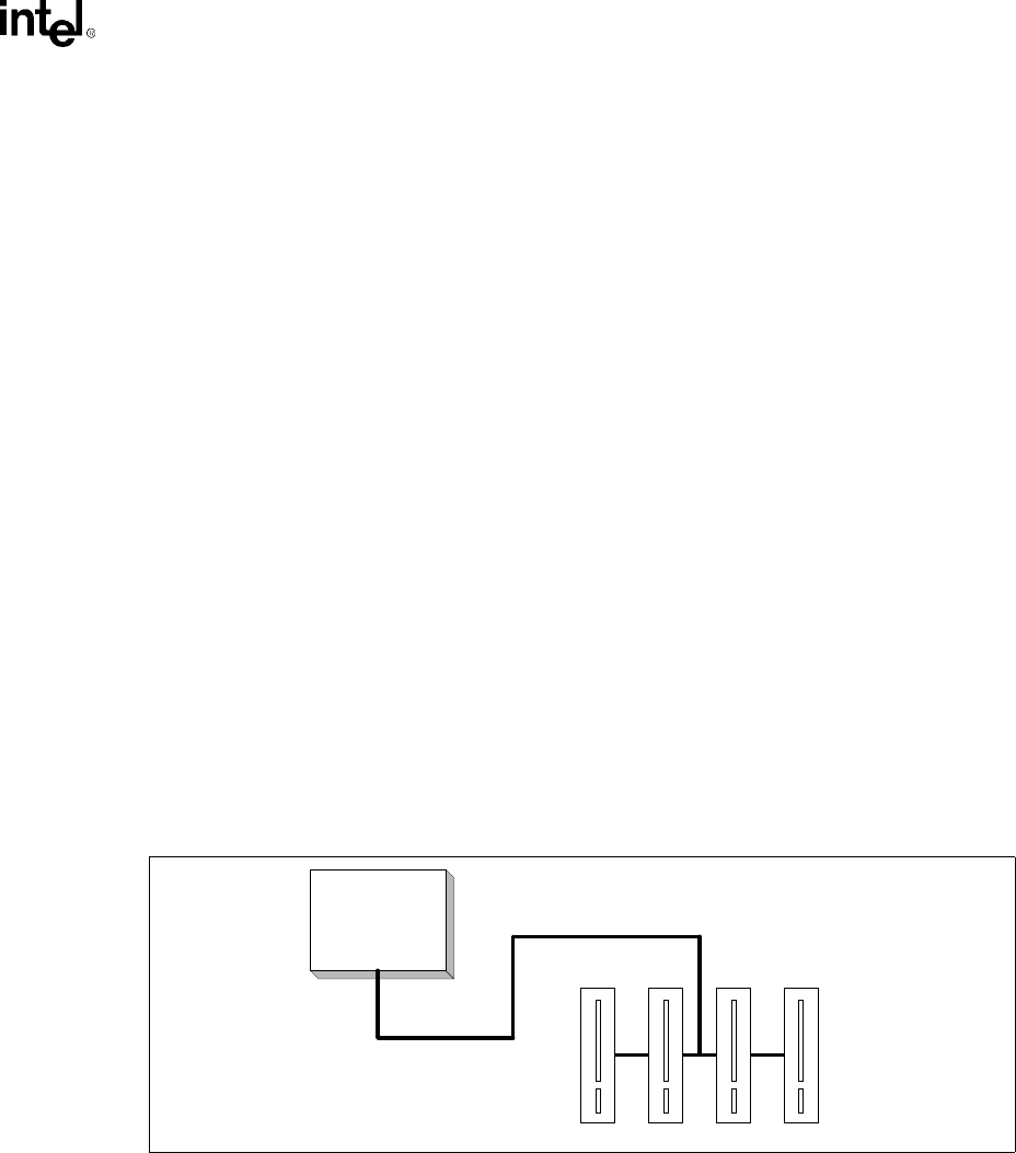
Intel®820 Chipset Design Guide 2-67
Layout/Routing Guidelines
2.18 SMBus/Alert Bus
The Alert on LAN* signals can be used as:
•Alert on LAN* signals: 4.7 KΩ pullup resistors to 3.3VSB are required.
•GPIOs: Pullup resistors to 3.3VSB and the signals must be allowed to
change states on powerup (e.g., on power-up, the ICH drives
heartbeat messages until the BIOS programs these signals as
GPIOs). The value of the pullup resistors depends on the loading on
the GPIO signal.
•Not Used: 4.7 KΩ pullup resistors to 3.3VSB are required.
If the SMBus is used only for the three SPD EEPROMs (one on each RIMM), both signals should
be pulled up with a 4.7 KΩ resistor to 3.3V.
2.19 PCI
The ICH provides a PCI Bus interface that is compliant with the PCI Local Bus Specification
Revision 2.2. The implementation is optimized for high-performance data streaming when the ICH
is acting as either the target or the initiator on the PCI bus. For more information on the PCI Bus
interface, refer to the PCI Local Bus Specification Revision 2.2.
The ICH supports six PCI Bus masters (excluding the ICH), by providing six REQ#/GNT# pairs.
In addition, the ICH supports two PC/PCI REQ#/GNT# pairs, one of which is multiplexed with a
PCI REQ#/GNT# pair.
2.20 RTC
The ICH contains a real time clock (RTC) with 256 bytes of battery backed SRAM. The internal
RTC module provides two key functions: keeping date and time, and storing system data in its
RAM when the system is powered down.
This section will present the recommended hookup for the RTC circuit for the ICH. This circuit is
not the same as the circuit used for the PIIX4.
Figure 2-55. PCI Bus Layout Example
ICH
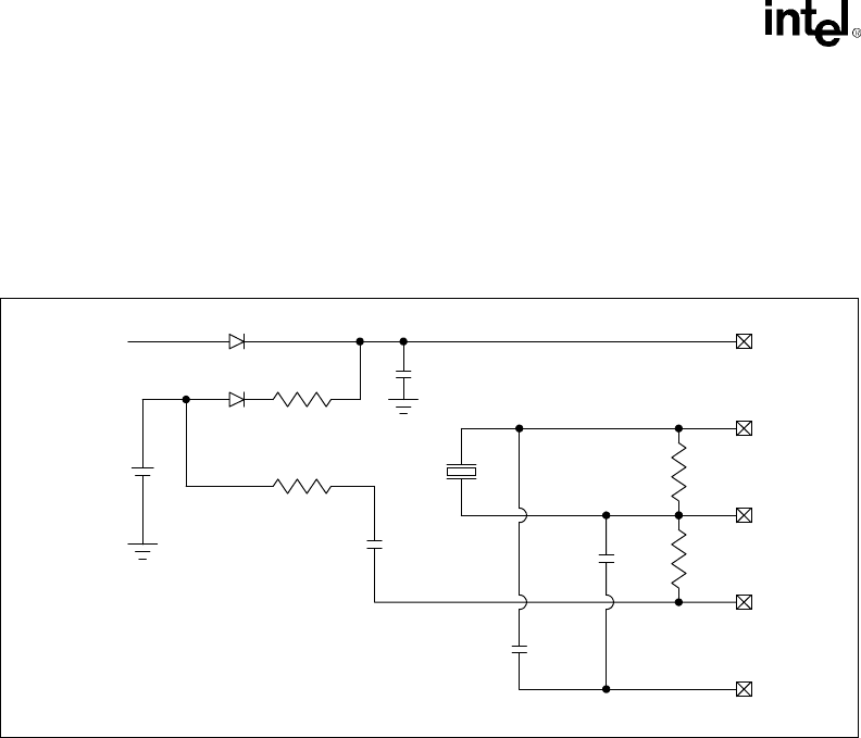
Layout/Routing Guidelines
2-68 Intel®820 Chipset Design Guide
2.20.1 RTC Crystal
The ICH RTC module requires an external oscillating source of 32.768 KHz connected on the
RTCX1 and RTCX2 pins. Figure 2-56 documents the external circuitry that comprises the
oscillator of the ICH RTC.
NOTES:
1. The exact capacitor value needs to based on what the crystal maker recommends.
2. This circuit is not the same as the one used for PIIX4.
3. VCCRTC: Power for RTC Well
4. RTCX2: Crystal Input 2 – Connected to the 32.768 KHz crystal.
5. RTCX1: Crystal Input 1 – Connected to the 32.768 KHz crystal.
6. VBIAS: RTC BIAS Voltage – This pin is used to provide a reference voltage, and this DC voltage sets a
current which is mirrored throughout the oscillator and buffer circuitry.
7. VSS: Ground
2.20.2 External Capacitors
To maintain the RTC accuracy, the external capacitor C1 needs to be 0.047 uF, and the external
capacitor values (C2 and C3) should be chosen to provide the manufacturer’s specified load
capacitance (Cload) for the crystal when combined with the parasitic capacitance of the trace,
socket (if used), and package. When the external capacitor values are combined with the
capacitance of the trace, socket, and package, the closer the capacitor value can be matched to the
actual load capacitance of the crystal used, the more accurate the RTC will be.
Equation 2-4 can be used to choose the external capacitance values (C2 and C3):
Equation 2-4. External Capacitance Calculation
Cload = (C2 * C3)/(C2+C3) + Cparasitic
C3 can be chosen such that C3 > C2. Then C2 can be trimmed to obtain the 32.768 kHz.
Figure 2-56. External Circuitry for the ICH RTC2
C3
1
VCC3_3SBY
1 k
Ω
Vbat_rtc 1 k
Ω
C1
0.047 uF
32768 Hz
Xtal R1
10 M
Ω
R2
10 M
Ω
C2
1
1
µ
F
VCCRTC
3
RTCX2
4
RTCX1
5
VBIAS
6
VSS
7
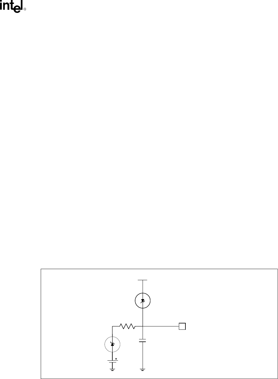
Intel®820 Chipset Design Guide 2-69
Layout/Routing Guidelines
2.20.3 RTC Layout Considerations
•Keep the RTC lead lengths as short as possible; around ¼ inch is sufficient.
•Minimize the capacitance between Xin and Xout in the routing.
•Put a ground plane under the XTAL components.
•Do not route switching signals under the external components (unless on the other side of the
board).
•The oscillator VCC should be clean; use a filter, such as an RC lowpass, or a ferrite inductor.
2.20.4 RTC External Battery Connection
The RTC requires an external battery connection to maintain its functionality and its RAM while
the ICH is not powered by the system.
Example batteries are Duracell 2032, 2025, or 2016 (or equivalent), which can give many years of
operation. Batteries are rated by storage capacity. The battery life can be calculated by dividing the
capacity by the average current required. For example, if the battery storage capacity is 170 mAh
(assumed usable) and the average current required is 3 uA, the battery life will be at least:
170,000 uAh / 3 uA = 56,666 h = 6.4 years
The voltage of the battery can affect the RTC accuracy. In general, when the battery voltage
decays, the RTC accuracy also decreases. High accuracy can be obtained when the RTC voltage is
in the range of 3.0V to 3.3V.
The battery must be connected to the ICH via an isolation schottky diode circuit. The schottky
diode circuit allows the ICH RTC-well to be powered by the battery when the system power is not
available, but by the system power when it is available. To do this, the diodes are set to be reverse
biased when the system power is not available. Figure 2-57 is an example of a diode circuitry that
is used.
A standby power supply should be used in a desktop system to provide continuous power to the
RTC when available, which will significantly increase the RTC battery life and thereby increase the
RTC accuracy.
Figure 2-57. Diode Circuit Connecting RTC External Battery
VCC3_3SBY
VccRTC
1.0 uF
1 K
Ω
rtc e t bat sd
Layout/Routing Guidelines
2-70 Intel®820 Chipset Design Guide
2.20.5 RTC External RTCRST Circuit
The ICH RTC requires some additional external circuitry. The RTCRST# signal is used to reset the
RTC well. The external capacitor and the external resistor between RTCRST# and the RTC battery
(Vbat) were selected to create an RC time delay, such that RTCRST# will go high some time after
the battery voltage is valid. The RC time delay should be in the range of 10-20 ms. When
RTCRST# is asserted, bit 2 (RTC_PWR_STS) in the GEN_PMCON_3 (General PM Configuration
3) register is set to 1, and remains set until software clears it. As a result of this, when the system
boots, the BIOS knows that the RTC battery has been removed.
This RTCRST# circuit is combined with the diode circuit (Figure 2-57) which allows the RTC well
to be powered by the battery when the system power is not available. Figure 2-56 is an example of
this circuitry that is used in conjuction with the external diode circuit.
2.20.6 RTC Routing Guidelines
•All RTC OSC signals (RTCX1, RTCX2, VBIAS) should all be routed with trace lengths of
less than 1”, the shorter the better
•Minimize the capacitance between RTCX1 and RTCX2 in the routing (optimal would be a
ground line between them)
•Put a ground plane under all of the external RTC circuitry
•Do not route any switching signals under the external components (unless on the other side of
the ground plane)
Figure 2-58. RTCRST External Circuit for the ICH RTC
VCC3_3SBY
VccRTC
1.0 uF
1K
2.2 uF
8.2K RTCRST#
RTCRST
Circuit
Diode/
Battery
Circuit

Intel®820 Chipset Design Guide 2-71
Layout/Routing Guidelines
2.20.7 VBIAS DC Voltage and Noise Measurements
•Steady state VBIAS will be a DC voltage of about 0.38V ±0.06V.
•VBIAS will be “kicked” when the battery is inserted to about 0.7–1.0V, but it will come back
to its DC value within a few ms.
•Noise on VBIAS must be kept to a minimum, 200 mV or less.
•VBIAS is very sensitive and cannot be directly probed; it can be probed through a 0.01 uF
capacitor.
•Excess noise on VBIAS can cause the ICH internal oscillator to misbehave or even stop
completely.
•To minimize noise of VBIAS, it is necessary to implement the routing guidelines described
above and the required external RTC circuitry.

Layout/Routing Guidelines
2-72 Intel®820 Chipset Design Guide
This page is intentionally left blank.

3
Advanced System Bus
Design
This page is intentionally left blank.

Intel®820 Chipset Design Guide 3-1
Advanced System Bus Design
Advanced System Bus Design 3
Section 2.9, “System Bus Design” on page 2-46 describes the recommendations for designing
Intel® 820 chipset based platforms. This chapter discusses more detail about the methodology used
to develop the guidelines. Section 3.2, “AGTL+ Design Guidelines” on page 3-4 discusses specific
system guidelines. This is a step-by-step methodology that Intel has successfully used to design
high performance desktop systems. Section 3.3, “Theory” on page 3-15 introduces the theories that
are applicable to this layout guideline. Section 3.4, “More Details and Insight” on page 3-19
contains more details and insights. The items in Section 3.4 expand on some of the rationale for the
recommendations in the step-by-step methodology. This section also includes equations that may
be used for reference.
3.1 Terminology and Definitions
Term Definition
Aggressor A network that transmits a coupled signal to another network is called the
aggressor network.
AGTL+ The processor system bus uses a bus technology called AGTL+, or Assisted
Gunning Transceiver Logic. AGTL+ buffers are open-drain and require pull-up
resistors for providing the high logic level and termination. The processor
AGTL+ output buffers differ from GTL+ buffers with the addition of an active
pMOS pull-up transistor to “assist” the pull-up resistors during the first clock of
a low-to-high voltage transition. Additionally, the processor Single Edge
Connector (S.E.C.) cartridge contains 56 Ω pull-up resistors to provide
termination at each bus load.
Bus Agent A component or group of components that, when combined, represent a single
load on the AGTL+ bus.
Corner Describes how a component performs when all parameters that could impact
performance are adjusted to have the same impact on performance. Examples of
these parameters include variations in manufacturing process, operating
temperature, and operating voltage. The results in performance of an electronic
component that may change as a result of corners include (but are not limited
to): clock to output time, output driver edge rate, output drive current, and input
drive current. Discussion of the “slow” corner would mean having a component
operating at its slowest, weakest drive strength performance. Similar discussion
of the “fast” corner would mean having a component operating at its fastest,
strongest drive strength performance. Operation or simulation of a component at
its slow corner and fast corner is expected to bound the extremes between
slowest, weakest performance and fastest, strongest performance.

Advanced System Bus Design
3-2 Intel®820 Chipset Design Guide
Cross-talk The reception on a victim network of a signal imposed by aggressor network(s)
through inductive and capacitive coupling between the networks.
•Backward Cross-talk - coupling which creates a signal in a victim network
that travels in the opposite direction as the aggressor’s signal.
•Forward Cross-talk - coupling which creates a signal in a victim network
that travels in the same direction as the aggressor’s signal.
•Even Mode Cross-talk - coupling from multiple aggressors when all the
aggressors switch in the same direction that the victim is switching.
•Odd Mode Cross-talk - coupling from multiple aggressors when all the
aggressors switch in the opposite direction that the victim is switching.
Edge Finger The cartridge electrical contact that interfaces to the SC242 connector.
Flight Time Flight Time is a term in the timing equation that includes the signal propagation
delay, any effects the system has on the TCO of the driver, plus any adjustments
to the signal at the receiver needed to guarantee the setup time of the receiver.
More precisely, flight time is defined to be:
•The time difference between a signal at the input pin of a receiving agent
crossing VREF (adjusted to meet the receiver manufacturer’s conditions
required for AC timing specifications; i.e., ringback, etc.), and the output
pin of the driving agent crossing VREF if the driver was driving the Test
Load used to specify the driver’s AC timings.
See Section for details regarding flight time simulation and validation.
The VREF Guardband takes into account sources of noise that may affect the
way an AGTL+ signal becomes valid at the receiver. See the definition of
the VREF Guardband.
•Maximum and Minimum Flight Time - Flight time variations can be
caused by many different parameters. The more obvious causes include
variation of the board dielectric constant, changes in load condition, cross-
talk, VTT noise, VREF noise, variation in termination resistance and
differences in I/O buffer performance as a function of temperature, voltage
and manufacturing process. Some less obvious causes include effects of
Simultaneous Switching Output (SSO) and packaging effects.
•The Maximum Flight Time is the largest flight time a network will
experience under all variations of conditions. Maximum flight time is
measured at the appropriate VREF Guardband boundary.
•The Minimum Flight Time is the smallest flight time a network will
experience under all variations of conditions. Minimum flight time is
measured at the appropriate VREF Guardband boundary.
For more information on flight time and the VREF Guardband, see the
Pentium®II Processor Developer’s Manual.
GTL+ GTL+ is the bus technology used by the Pentium® Pro processor. This is an
incident wave switching, open-drain bus with pull-up resistors that provide both
the high logic level and termination. It is an enhancement to the GTL (Gunning
Transceiver Logic) technology. See thePentium® II Processor Developer’s
Manual for more details of GTL+.
Term Definition

Intel®820 Chipset Design Guide 3-3
Advanced System Bus Design
Network The trace of a Printed Circuit Board (PCB) that completes an electrical
connection between two or more components.
Network
Length The distance between extreme bus agents on the network and does not include
the distance connecting the end bus agents to the termination resistors.
Overdrive
Region Is the voltage range, at a receiver, located above and below VREF for signal
integrity analysis. See the Intel® Pentium®II Processor Developer’s Manual for
more details.
Overshoot Maximum voltage allowed for a signal at the processor core pad. See each
processor’s datasheet for overshoot specification.
Pad A feature of a semiconductor die contained within an internal logic package on
the S.E.C cartridge substrate used to connect the die to the package bond wires.
A pad is only observable in simulation.
Pin A feature of a logic package contained within the S.E.C. cartridge used to
connect the package to an internal substrate trace.
Ringback Ringback is the voltage that a signal rings back to after achieving its maximum
absolute value. Ringback may be due to reflections, driver oscillations, etc. See
the respective processor’s datasheet for ringback specification.
Settling Limit Defines the maximum amount of ringing at the receiving pin that a signal must
reach before its next transition. See the respective processor’s datasheet for
settling limit specification.
Setup Window Is the time between the beginning of Setup to Clock (TSU_MIN) and the arrival of
a valid clock edge. This window may be different for each type of bus agent in
the system.
Simultaneous
Switching
Output (SSO)
Effects
Refers to the difference in electrical timing parameters and degradation in signal
quality caused by multiple signal outputs simultaneously switching voltage
levels (e.g., high-to-low) in the opposite direction from a single signal (e.g., low-
to-high) or in the same direction (e.g., high-to-low). These are respectively
called odd-mode switching and even-mode switching. This simultaneous
switching of multiple outputs creates higher current swings that may cause
additional propagation delay (or “pushout”), or a decrease in propagation delay
(or “pull-in”). These SSO effects may impact the setup and/or hold times and are
not always taken into account by simulations. System timing budgets should
include margin for SSO effects.
Stub The branch from the trunk terminating at the pad of an agent.
Test Load Intel uses a 50 Ω test load for specifying its components.
Trunk The main connection, excluding interconnect branches, terminating at agent
pads.
Undershoot Maximum voltage allowed for a signal to extend below VSS at the processor core
pad. See the respective processor’s datasheet for undershoot specifications.
Victim A network that receives a coupled cross-talk signal from another network is
called the victim network.
VREF Guardband A guardband (∆VREF) defined above and below VREF to provide a more realistic
model accounting for noise such as cross-talk, VTT noise, and VREF noise.
Term Definition

Advanced System Bus Design
3-4 Intel®820 Chipset Design Guide
3.2 AGTL+ Design Guidelines
The following step-by-step guideline was developed for systems based on two processor loads and
one Intel 82820 MCH load. Systems using custom chipsets will require timing analysis and analog
simulations specific to those components.
The guideline recommended in this section is based on experience developed at Intel while
developing many different Intel Pentium® Pro processor family and Intel Pentium III processor-
based systems. Begin with an initial timing analysis and topology definition. Perform pre-layout
analog simulations for a detailed picture of a working “solution space” for the design. These pre-
layout simulations help define routing rules prior to placement and routing. After routing, extract
the interconnect database and perform post-layout simulations to refine the timing and signal
integrity analysis. Validate the analog simulations when actual systems become available. The
validation section describes a method for determining the flight time in the actual system.
Guideline Methodology:
•Initial Timing Analysis
•Determine General Topology, Layout, and Routing
•Pre-Layout Simulation
— Sensitivity sweep
— Monte Carlo Analysis
•Place and Route Board
— Estimate Component to Component Spacing for AGTL+ Signals
— Layout and Route Board
•Post-Layout Simulation
— Interconnect Extraction
— Inter-Symbol Interference (ISI), Cross-talk, and Monte Carlo Analysis
•Validation
—Measurements
— Determining Flight Time

Intel®820 Chipset Design Guide 3-5
Advanced System Bus Design
3.2.1 Initial Timing Analysis
Perform an initial timing analysis of the system using Equation 3-1 and Equation 3-2 shown below.
These equations are the basis for timing analysis. To complete the initial timing analysis, values for
clock skew and clock jitter are needed, along with the component specifications. These equations
contain a multi-bit adjustment factor, MADJ, to account for multi-bit switching effects such as SSO
pushout or pull-in that are often hard to simulate. These equations do not take into consideration all
signal integrity factors that affect timing. Additional timing margin should be budgeted to allow for
these sources of noise.
Equation 3-1. Setup Time
TCO_MAX + TSU_MIN + CLKSKEW + CLKJITTER + TFLT_MAX + MADJ ≤ Clock Period
Equation 3-2. Hold Time
TCO_MIN + TFLT_MIN - MADJ ≥ THOLD + CLKSKEW
Symbols used in Equation 3-1 and Equation 3-2:
—T
CO_MAX is the maximum clock to output specification1.
—T
SU_MIN is the minimum required time specified to setup before the clock1.
—CLK
JITTER is the maximum clock edge-to-edge variation.
—CLK
SKEW is the maximum variation between components receiving the same clock edge.
—T
FLT_MAX is the maximum flight time as defined in Section 3.1, “Terminology and
Definitions” on page 3-1.
—T
FLT_MIN is the minimum flight time as defined in Section 3.1, “Terminology and
Definitions” on page 3-1.
—M
ADJ is the multi-bit adjustment factor to account for SSO pushout or pull-in.
—T
CO_MIN is the minimum clock to output specification1.
—T
HOLD is the minimum specified input hold time.
Note: The Clock to Output (TCO) and Setup to Clock (TSU) timings are both measured from the signals
last crossing of VREF, with the requirement that the signal does not violate the ringback or edge
rate limits. See the respective Processor’s datasheet and thePentium® III Processor Developer’s
Manual for more details.
Solving these equations for TFLT results in the following equations:
Equation 3-3. Maximum Flight Time
TFLT_MAX ≤ Clock Period - TCO_MAX - TSU_MIN - CLKSKEW - CLKJITTER - MADJ
Equation 3-4. Minimum Flight Time
TFLT_MIN ≥ THOLD + CLKSKEW - TCO_MIN + MADJ

Advanced System Bus Design
3-6 Intel®820 Chipset Design Guide
There are multiple cases to consider. Note that while the same trace connects two components,
component A and component B, the minimum and maximum flight time requirements for
component A driving component B as well as component B driving component A must be met. The
cases to be considered are:
•Processor driving processor
•Processor driving chipset
•Chipset driving processor
A designer using components other than those listed above must evaluate additional combinations
of driver and receiver.
NOTES:
1. All times in nanoseconds.
2. Numbers in table are for reference only. These timing parameters are subject to change. Please check the
appropriate component documentation for valid timing parameter values.
3. TSU_MIN = 1.9 ns assumes the 82820 MCH sees a minimum edge rate equal to 0.3 V/ns.
4. The Pentium III substrate nominal impedance is set to 65 Ω ±15%. Future Pentium III processor substrate
may be set at 60 Ω ±15%
Table 3-1 lists the AGTL+ component timings of the processors and 82820 MCH defined at the
pins. These timings are for reference only.
Table 3-2 gives an example AGTL+ initial maximum flight time and Table 3-3 is an example
minimum flight time calculation for a 133 MHz, 2-way Pentium III processor/Intel 820 chipset
system bus. Note that assumed values for clock skew and clock jitter were used. Clock skew and
clock jitter values are dependent on the clock components and distribution method chosen for a
particular design and must be budgeted into the initial timing equations as appropriate for each
design.
Intel highly recommends adding margin as shown in the “MADJ” column to offset the degradation
caused by SSO push-out and other multi-bit switching effects. The “Recommended TFLT_MAX”
column contains the recommended maximum flight time after incorporating the MADJ value. If
edge rate, ringback, and monotonicity requirements are not met, flight time correction must first be
performed as documented in the Pentium®II Processor Developer’s Manual with the additional
requirements noted in Section 3.5, “Definitions of Flight Time Measurements/Corrections and
Signal Quality” on page 3-24. The commonly used “textbook” equations used to calculate the
expected signal propagation rate of a board are included in Section 3.2, “AGTL+ Design
Guidelines” on page 3-4.
Simulation and control of baseboard design parameters can ensure that signal quality and
maximum and minimum flight times are met. Baseboard propagation speed is highly dependent on
transmission line geometry configuration (stripline vs. microstrip), dielectric constant, and loading.
This layout guideline includes high-speed baseboard design practices that may improve the amount
Table 3-1. AGTL+ Parameters for Example Calculations1,2
IC Parameters Intel® Pentium® III
processor core at
133 MHz Bus
Intel 82820
MCH Notes
Clock to Output maximum (TCO_MAX)2.73.64
Clock to Output minimum (TCO_MIN)-0.10.54
Setup time (TSU_MIN) 1.2 2.27 3,4
Hold time (THOLD) 0.8 0.28 4

Intel®820 Chipset Design Guide 3-7
Advanced System Bus Design
of timing and signal quality margin. The magnitude of MADJ is highly dependent on baseboard
design implementation (stackup, decoupling, layout, routing, reference planes, etc.) and needs to
be characterized and budgeted appropriately for each design.
Table 3-2 and Table 3-3 are derived assuming:
•CLKSKEW = 0.2 ns (Note: Assumes clock driver pin-to-pin skew is reduced to 50 ps by tying
two host clock outputs together (“ganging”) at clock driver output pins, and the PCB clock
routing skew is 150 ps. System timing budget must assume 0.175 ns of clock driver skew if
outputs are not tied together and a clock driver that meets the CK98 clock driver specification
is being used.)
•CLKJITTER = 0.250 ns
Some clock driver components may not support ganging the outputs together. Be sure to
verify with your clock component vendor before ganging the outputs. See the appropriate Intel
820 chipset documentation for details on clock skew and jitter specifications. Refer to
Section 2.6.2, “Direct Rambus* Layout Guidelines” on page 2-8 and Chapter 4, “Clocking” for
host clock routing details.
NOTES:
1. All times in nanoseconds.
2. BCLK period = 7.50 ns @ 133.33 MHz.
3. The flight times in this column include margin to account for the following phenomena that Intel has observed
when multiple bits are switching simultaneously. These multi-bit effects can adversely affect flight time and
signal quality and are sometimes not accounted for in simulation. Accordingly, maximum flight times depend
on the baseboard design and additional adjustment factors or margins are recommended.
- SSO push-out or pull-in.
- Rising or falling edge rate degradation at the receiver caused by inductance in the current return
path, requiring extrapolation that causes additional delay.
- Cross-talk on the PCB and internal to the package can cause variation in the signals.
There are additional effects that may not necessarily be covered by the multi-bit adjustment factor and
should be budgeted as appropriate to the baseboard design. Examples include:
- The effective board propagation constant (SEFF), which is a function of:
•Dielectric constant (εr) of the PCB material.
• The type of trace connecting the components (stripline or microstrip).
• The length of the trace and the load of the components on the trace. Note that the board propagation
constant multiplied by the trace length is a component of the flight time but not necessarily equal
to the flight time.
4. Processor values specified in this table are examples only. Refer to the appropriate processor datasheet for
specification values.
Table 3-2. Example TFLT_MAX Calculations for 133 MHz Bus1
Driver Receiver Clk
Period2TCO_MAX TSU_MIN ClkSKEW ClkJITTER MAD
J
Recommended
TFLT_MAX3
Processor4Processor47.50 2.7 1.20 0.20 0.250 0.40 2.75
Processor482820 MCH 7.50 2.7 2.27 0.20 0.250 0.40 1.68
82820 MCH Processor47.50 3.63 1.20 0.20 0.25 0.40 1.82

Advanced System Bus Design
3-8 Intel®820 Chipset Design Guide
NOTES:
1. All times in nanoseconds.
2. Processor values specified in this table are examples only. Refer to the appropriate processor datasheet for
specification values.
3.2.2 Determine General Topology, Layout, and Routing Desired
After calculating the timing budget, determine the approximate location of the processor and the
chipset on the base board (see Section 2.9, “System Bus Design” on page 2-46).
3.2.3 Pre-Layout Simulation
3.2.3.1 Methodology
Analog simulations are recommended for high speed system bus designs. Start simulations prior to
layout. Pre-layout simulations provide a detailed picture of the working “solution space” that meets
flight time and signal quality requirements. The layout recommendations in the previous sections
are based on pre-layout simulations conducted at Intel. By basing board layout guidelines on the
solution space, the iterations between layout and post-layout simulation can be reduced.
Intel recommends running simulations at the device pads for signal quality and at the device pins
for timing analysis. However, simulation results at the device pins may be used later to correlate
simulation performance against actual system measurements.
3.2.3.2 Sensitivity Analysis
Pre-layout analysis includes a sensitivity analysis using parametric sweeps. Parametric sweep
analysis involves varying one or two system parameters while all others such as driver strength,
package, Z0, and S0 are held constant. This way, the sensitivity of the proposed bus topology to
varying parameters can be analyzed systematically. Sensitivity of the bus to minimum flight time,
maximum flight time, and signal quality should be covered. Suggested sweep parameters include
trace lengths, termination resistor values, and any other factors that may affect flight time, signal
quality, and feasibility of layout. Minimum flight time and worst signal quality are typically
analyzed using fast I/O buffers and interconnect. Maximum flight time is typically analyzed using
slow I/O buffers and slow interconnects.
Outputs from each sweep should be analyzed to determine which regions meet timing and signal
quality specifications. To establish the working solution space, find the common space across all
the sweeps that result in passing timing and signal quality. The solution space should allow enough
design flexibility for a feasible, cost-effective layout.
Table 3-3. Example TFLT_MIN Calculations (Frequency Independent)
Driver Receiver THOLD ClkSKEW TCO_MIN
Recommended
TFLT_MIN
Processor2Processor20.8 0.2 -0.1 1.2
Processor282820 MCH 0.28 0.2 -0.1 .58
82820 MCH Processor20.8 0.2 0.5 .5

Intel®820 Chipset Design Guide 3-9
Advanced System Bus Design
3.2.3.3 Monte Carlo Analysis
Perform a Monte Carlo analysis to refine the passing solution space region. A Monte Carlo analysis
involves randomly varying parameters (independent of one another) over their tolerance range.
This analysis intends to ensure that no regions of failing flight time and signal quality exists
between the extreme corner cases run in pre-layout simulations. For the example topology, vary the
following parameters during Monte Carlo simulations:
•Lengths L1 through L3
•Termination resistance RTT on the processor cartridge #1
•Termination resistance RTT on the processor cartridge #2
•Z0 of traces on processor cartridge #1
•Z0 of traces on processor cartridge #2
•S0 of traces on processor cartridge #1
•S0 of traces on processor cartridge #2
•Z0 of traces on baseboard
•S0 of traces on baseboard
•Fast and slow corner processor I/O buffer models for cartridge #1
•Fast and slow corner processor I/O buffer models for cartridge #2
•Fast and slow package models for processor cartridge #1
•Fast and slow package models for processor cartridge #2
•Fast and slow corner 82820 MCH I/O buffer models
•Fast and slow 82820 MCH package models
3.2.3.4 Simulation Criteria
Accurate simulations require that the actual range of parameters be used in the simulations. Intel
has consistently measured the cross-sectional resistivity of the PCB copper to be approximately
1Ω*mil2/inch, not the 0.662 Ω*mil2/inch value for annealed copper that is published in reference
material. Using the 1 Ω*mil2/inch value may increase the accuracy of lossy simulations.
Positioning drivers with faster edges closer to the middle of the network typically results in more
noise than positioning them towards the ends. However, Intel has shown that drivers located in all
positions (given appropriate variations in the other network parameters) can generate the worst-
case noise margin. Therefore, Intel recommends simulating the networks from all driver locations,
and analyzing each receiver for each possible driver.
Analysis has shown that both fast and slow corner conditions must be run for both rising and
falling edge transitions. The fast corner is needed because the fast edge rate creates the most noise.
The slow corner is needed because the buffer’s drive capability will be a minimum, causing the VOL
to shift up, which may cause the noise from the slower edge to exceed the available budget. Slow
corner models may produce minimum flight time violations on rising edges if the transition starts
from a higher VOL. So, Intel highly recommends checking for minimum and maximum flight time
violations with both the fast and slow corner models. The fast and slow corner I/O buffer models
are contained in the processor and Intel 820 chipset electronic models provided by Intel.
The transmission line package models must be inserted between the output of the buffer and the net
it is driving. Likewise, the package model must also be placed between a net and the input of a
receiver model. Editing the simulator’s net description or topology file generally does this.

Advanced System Bus Design
3-10 Intel®820 Chipset Design Guide
Intel has found wide variation in noise margins when varying the stub impedance and the PCB’s
Z0 and S0. Intel therefore recommends that PCB parameters are controlled as tightly as possible,
with a sampling of the allowable Z0 and S0 simulated. The Intel® Pentium® III processor nominal
effective line impedance is 65 Ω ±15%. Future Intel® Pentium® III processor effective line
impedance (ZEFF) may be 60 Ω ±15%. Intel recommends the baseboard nominal effective line
impedance to be at 60 Ω ±15% for the recommended layout guidelines to be effective. Intel also
recommends running uncoupled simulations using the Z0 of the package stubs; and performing
fully coupled simulations if increased accuracy is needed or desired. Accounting for cross-talk
within the device package by varying the stub impedance was investigated and was not found to be
sufficiently accurate. This lead to the development of full package models for the component
packages.
3.2.4 Place and Route Board
3.2.4.1 Estimate Component To Component Spacing for AGTL+ Signals
Estimate the number of layers that will be required. Then determine the expected interconnect
distances between each of the components on the AGTL+ bus. Using the estimated interconnect
distances, verify that the placement can support the system timing requirements.
The required bus frequency and the maximum flight time propagation delay on the PCB determine
the maximum network length between the bus agents. The minimum network length is independent
of the required bus frequency. Table 3-2 and Table 3-3 assume values for CLKSKEW and
CLKJITTER - parameters that are controlled by the system designer. To reduce system clock skew to
a minimum, clock buffers that allow their outputs to be tied together are recommended. Intel
strongly recommends running analog simulations to ensure that each design has adequate noise and
timing margin.
3.2.4.2 Layout and Route Board
Route the board satisfying the estimated space and timing requirements. Also stay within the
solution space set from the pre-layout sweeps. Estimate the printed circuit board parameters from
the placement and other information including the following general guidelines:
•Distribute VTT with a power plane or a partial power plane. If this cannot be accomplished,
use as wide a trace as possible and route the VTT trace with the same topology as the AGTL+
traces.
•Keep the overall length of the bus as short as possible (but do not forget minimum component-
to-component distances to meet hold times).
•Plan to minimize cross-talk with the following guidelines developed for the example topology
given (signal spacing recommendations were based on fully coupled simulations - spacing
may be decreased based upon the amount of coupled length):
— Use a spacing to line width to dielectric thickness ratio of at least 3:1:2. If εr = 4.5, this
should limit coupling to 3.4%.
— Minimize the dielectric process variation used in the PCB fabrication.
— Eliminate parallel traces between layers not separated by a power or ground plane.
Figure 3-3 contains the trace width:space ratios assumed for this topology. The cross-talk cases
considered in this guideline involve three types: Intragroup AGTL+, Intergroup AGTL+, and
AGTL+ to non-AGTL+. Intra-group AGTL+ cross-talk involves interference between AGTL+
signals within the same group (See Section 3.4, “More Details and Insight” on page 3-19 for a
description of the different AGTL+ group types). Intergroup AGTL+ cross-talk involves
Intel®820 Chipset Design Guide 3-11
Advanced System Bus Design
interference from AGTL+ signals in a particular group to AGTL+ signals in a different group. An
example of AGTL+ to non-AGTL+ cross-talk is when CMOS and AGTL+ signals interfere with
each other.
The spacing between the various bus agents causes variations in trunk impedance and stub
locations. These variations cause reflections that can cause constructive or destructive interference
at the receivers. A reduction of noise may be obtained by a minimum spacing between the agents.
Unfortunately, tighter spacing results in reduced component placement options and lower hold
margins. Therefore, adjusting the inter-agent spacing may be one way to change the network’s
noise margin, but mechanical constraints often limit the usefulness of this technique. Always be
sure to validate signal quality after making any changes in agent locations or changes to inter-agent
spacing.
There are six AGTL+ signals that can be driven by more than one agent simultaneously. These
signals may require more attention during the layout and validation portions of the design. When a
signal is asserted (driven low) by two or more agents on the same clock edge, the two falling edge
wave fronts will meet at some point on the bus and can sum to form a negative voltage. The ring-
back from this negative voltage can easily cross into the overdrive region. The signals are AERR#,
BERR#, BINIT#, BNR#, HIT#, and HITM#.
This document addresses AGTL+ layout for both 1 and 2-way 133 MHz/100 MHz processor/
Intel® 820 chipset systems. Power distribution and chassis requirements for cooling, connector
location, memory location, etc., may constrain the system topology and component placement
location; therefore, constraining the board routing. These issues are not directly addressed in this
document. Section 1.2, “References” on page 1-2 contains a listing of several documents that
address some of these issues.
Table 3-4. Trace Width Space Guidelines
Cross-talk Type Trace Width:Space Ratio
Intragroup AGTL+ (same group AGTL+) 5:10 or 6:12
Intergroup AGTL+ (different group AGTL+) 5:15 or 6:18
AGTL+ to non-AGTL+ 5:20 or 6:24
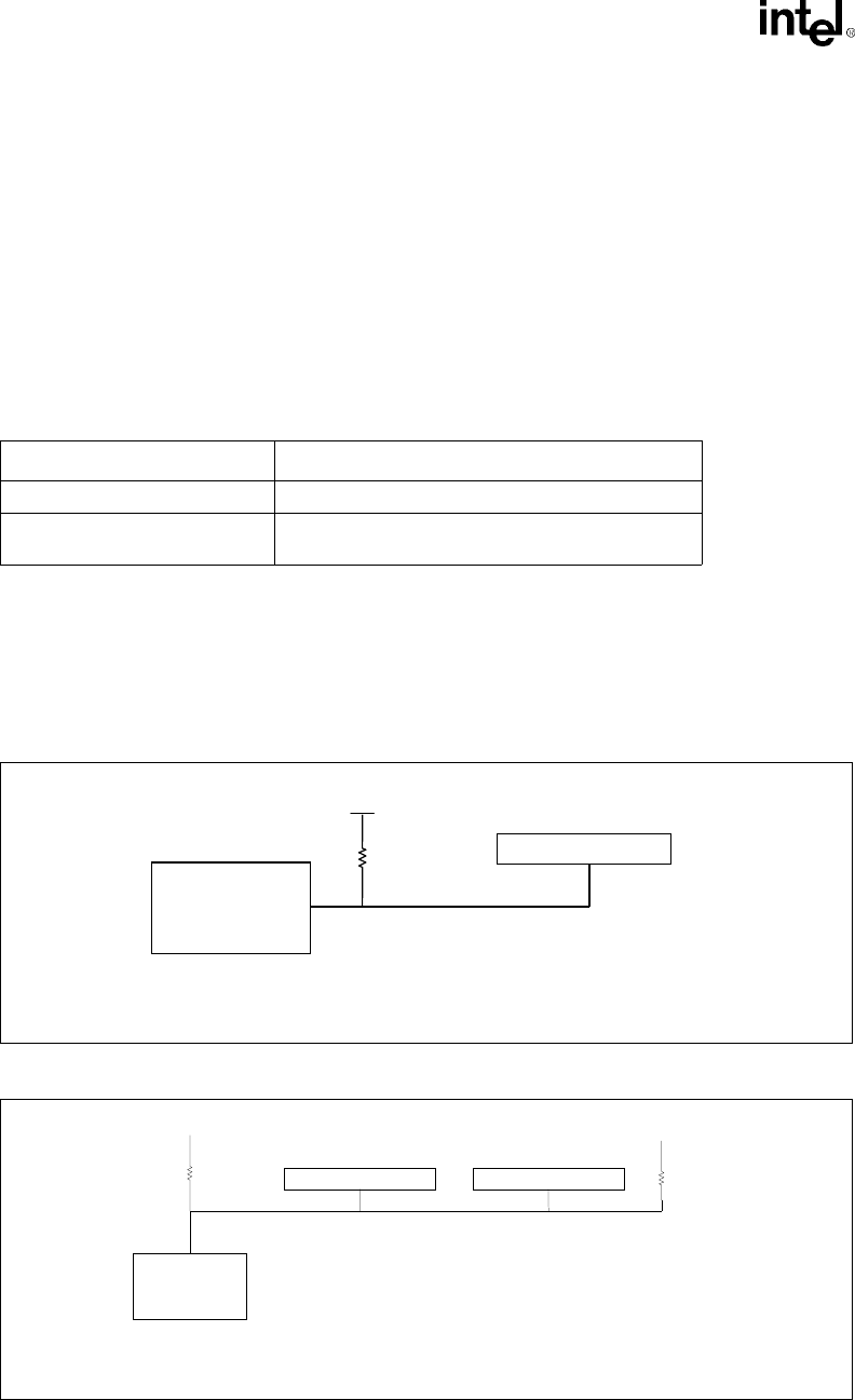
Advanced System Bus Design
3-12 Intel®820 Chipset Design Guide
3.2.4.3 Host Clock Routing
Host clock nets should be routed as point-to-point connections through a series resistor placed as
close to the output pins of the clock driver as possible. The value of the series resistor is dependent
on the clock driver characteristic impedance. However, a value of 33 Ω is a good starting point.
Table 3-5 provides the trace length recommendations for this topology. “H” indicates the length of
the host clock trace starting from the clock driver output pin and ending at the SC242 connector
BCLK pin. Note that the clock route from the clock driver to the Intel 82820 MCH will require an
additional trace length of approximately 4.6” to compensate for the additional propagation delay
along the processor host clock path (SC242 connector plus processor cartridge trace). This value of
4.6” assumes a propagation speed of 180 ps/in.
3.2.4.4 APIC Data Bus Routing
Intel recommends using the in-line topology shown in Figure 3-1 and Figure 3-2 for the APIC Data
signals, PICD[1:0]. For dual-processor systems, the network should be dual-end terminated with
330 Ω resistors. The combined routing lengths of L1 plus L2 should be between 0.0” and 12.0”.
Table 3-5. Host Clock Routing
Clock Net Trace length
Clock driver to SC242 connector H
Clock driver to Intel 82820 MCH H + (clock delay from the processor edge to core) +
connector delay
Figure 3-1. PICD[1,0] Uni-Processor Topology
Figure 3-2. PICD[1,0] Dual-Processor Topology
Intel
®
820
Chipset
SC242
L1 < 8"
L(1): Z0=60
Ω
±15%.
PICD[1,0]
2.5V
150 Ω
Intel
®
820
Chipset:
ICH
SC242
L1 + L2 < 12"
L(1): Z0=60
Ω
±15%.
PICD[1,0]
2.5V
330
Ω
SC242
2.5V
330
Ω
L1 L2

Intel®820 Chipset Design Guide 3-13
Advanced System Bus Design
3.2.5 Post-Layout Simulation
Following layout, extract the interconnect information for the board from the CAD layout tools.
Run simulations to verify that the layout meets timing and noise requirements. A small amount of
“tuning” may be required; experience at Intel has shown that sensitivity analysis dramatically
reduces the amount of tuning required. The post layout simulations should take into account the
expected variation for all interconnect parameters.
Intel specifies signal integrity at the device pads and therefore recommends running simulations at
the device pads for signal quality. However, Intel specifies core timings at the device pins, so
simulation results at the device pins should be used later to correlate simulation performance
against actual system measurements.
3.2.5.1 Intersymbol Interference
Intersymbol Interference (ISI) refers to the distortion or change in the waveform shape caused by
the voltage and transient energy on the network when the driver begins its next transition.
Intersymbol Interference (ISI) occurs when transitions in the current cycle interfere with transitions
in subsequent cycles. ISI can occur when the line is driven high, low, and then high in consecutive
cycles (the opposite case is also valid). When the driver drives high on the first cycle and low on
the second cycle, the signal may not settle to the minimum VOL before the next rising edge is driven.
This results in improved flight times in the third cycle. Intel performed ISI simulations for the
topology given in this section by comparing flight times for the first and third cycle. ISI effects do
not necessarily span only 3 cycles so it may be necessary to simulate beyond 3 cycles for certain
designs. After simulating and quantifying ISI effects, adjust the timing budget accordingly to take
these conditions into consideration.
3.2.5.2 Cross-Talk Analysis
AGTL+ cross-talk simulations can consider the processor core package, Intel 82820 MCH
package, and SC242 connectors as non-coupled. Treat the traces on the processor cartridge and
baseboard as fully coupled for maximum cross-talk conditions. Simulate the traces as lossless for
worst case cross-talk and lossy where more accuracy is needed. Evaluate both odd and even mode
cross-talk conditions.
AGTL+ Cross-talk simulation involves the following cases:
•Intra-group AGTL+ cross-talk
•Inter-group AGTL+ cross-talk
•Non-AGTL+ to AGTL+ cross-talk
3.2.5.3 Monte Carlo Analysis
Perform a Monte Carlo analysis on the extracted baseboard. Vary all parameters recommended for
the pre-layout Monte Carlo analysis within the region that they are expected to vary. The range for
some parameters will be reduced compared to the pre-layout simulations. For example, baseboard
lengths L1 through L7 should no longer vary across the full min and max range on the final
baseboard design. Instead, baseboard lengths should now have an actual route, with a length
tolerance specified by the baseboard fabrication manufacturer.
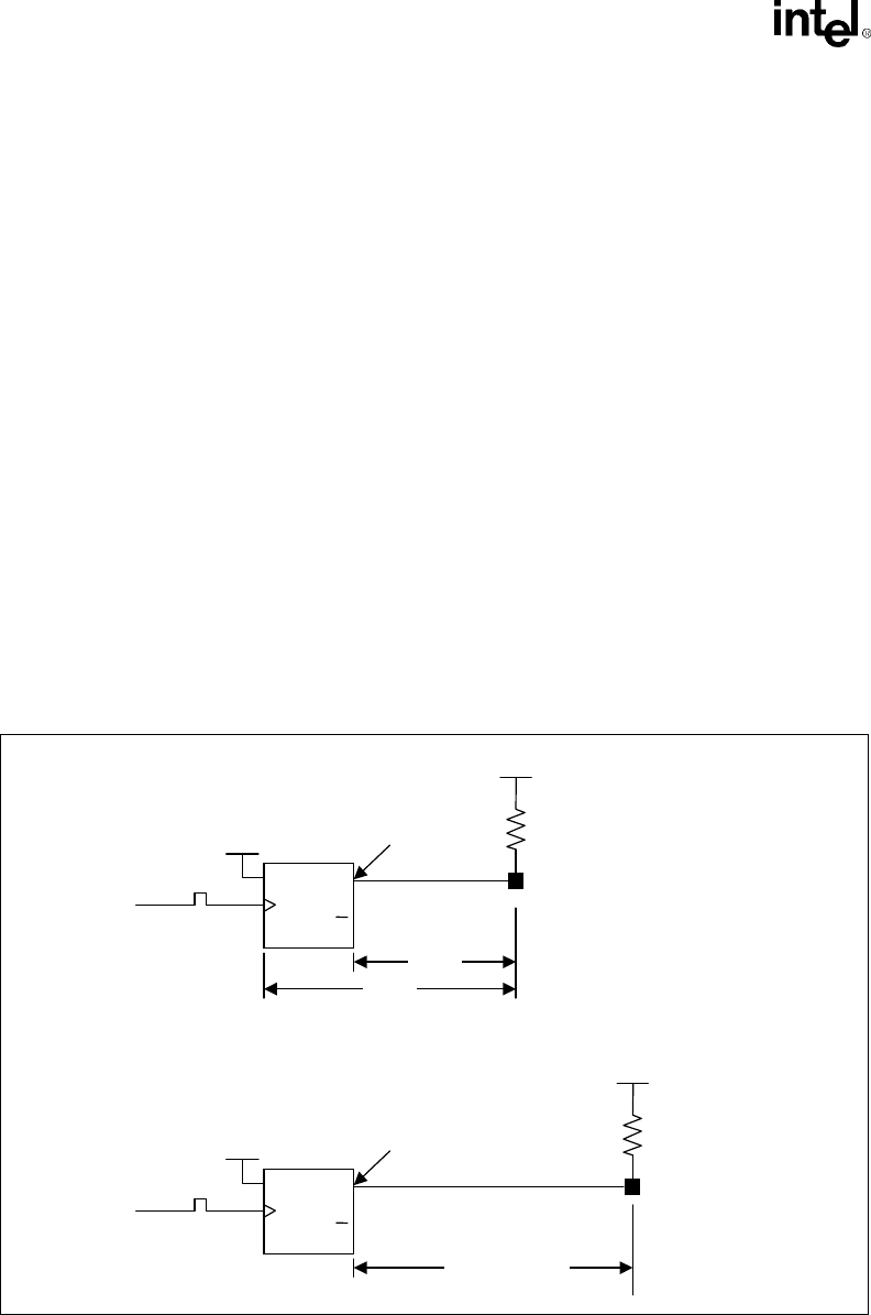
Advanced System Bus Design
3-14 Intel®820 Chipset Design Guide
3.2.6 Validation
Build systems and validate the design and simulation assumptions.
3.2.6.1 Measurements
Note that the AGTL+ specification for signal quality is at the pad of the component. The expected
method of determining the signal quality is to run analog simulations for the pin and the pad. Then
correlate the simulations at the pin against actual system measurements at the pin. Good correlation
at the pin leads to confidence that the simulation at the pad is accurate. Controlling the temperature
and voltage to correspond to the I/O buffer model extremes should enhance the correlation between
simulations and the actual system.
3.2.6.2 Flight Time Simulation
As defined in Section 3.1, “Terminology and Definitions” on page 3-1, flight time is the time
difference between a signal crossing VREF at the input pin of the receiver, and the output pin of the
driver crossing VREF were it driving a test load. The timings in the tables and topologies discussed
in this guideline assume the actual system load is 50 Ω and is equal to the test load. While the DC
loading of the AGTL+ bus in a DP mode is closer to 25 Ω, AC loading is approximately 29 Ω since
the driver effectively “sees” a 56 Ω termination resistor in parallel with a 60 Ω transmission line on
the cartridge.
Figure 3-3 above shows the different configurations for TCO testing and flight time simulation. The
flip-flop represents the logic input and driver stage of a typical AGTL+ I/O buffer. TCO timings are
specified at the driver pin output. TFLIGHT-SYSTEM is usually reported by a simulation tool as the
time from the driver pad starting its transition to the time when the receiver’s input pin sees a valid
data input. Since both timing numbers (TCO and TFLIGHT-SYSTEM) include propagation time from
the pad to the pin, it is necessary to subtract this time (TREF) from the reported flight time to avoid
Figure 3-3. Test Load vs. Actual System Load
V
TT
Q
Q
SET
CLR
D
Vcc
CLK
R
TEST
Test Load
Driver
Pin
Driver
Pad
TREF
TCO
I/O Buffer
Q
Q
SET
CLR
D
Vcc
CLK
Driver
Pad
TFLIGHTSYSTEM
I/O Buffer
V
TT
R
TT
Actual
System
Load
Receiver
Pin

Intel®820 Chipset Design Guide 3-15
Advanced System Bus Design
double counting. TREF is defined as the time that it takes for the driver output pin to reach the
measurement voltage, VREF, starting from the beginning of the driver transition at the pad. TREF
must be generated using the same test load for TCO. Intel provides this timing value in the AGTL+
I/O buffer models.
In this manner, the following valid delay equation is satisfied:
Equation 3-5. Valid Delay Equation
Valid Delay = TCO + TFLIGHT-SYS - TREF = TCO-MEASURED + TFLIGHT-MEASURED
This valid delay equation is the total time from when the driver sees a valid clock pulse to the time
when the receiver sees a valid data input.
3.2.6.3 Flight Time Hardware Validation
When a measurement is made on the actual system, TCO and flight time do not need TREF
correction since these are the actual numbers. These measurements include all of the effects
pertaining to the driver-system interface and the same is true for the TCO. Therefore the addition of
the measured TCO and the measured flight time must be equal to the valid delay calculated above.
3.3 Theory
3.3.1 AGTL+
AGTL+ is the electrical bus technology used for the processor bus. This is an incident wave
switching, open-drain bus with external pull-up resistors that provide both the high logic level and
termination at each load. The processor AGTL+ drivers contain a full-cycle active pull-up device
to improve system timings. The AGTL+ specification defines:
•Termination voltage (VTT).
•Receiver reference voltage (VREF) as a function of termination voltage (VTT).
• processor termination resistance (RTT).
•Input low voltage (VIL).
•Input high voltage (VIH).
•NMOS on resistance (RONN).
•PMOS on resistance (RONP).
•Edge rate specifications.
•Ringback specifications.
•Overshoot/Undershoot specifications.
•Settling Limit.

Advanced System Bus Design
3-16 Intel®820 Chipset Design Guide
3.3.2 Timing Requirements
The system timing for AGTL+ is dependent on many things. Each of the following elements
combine to determine the maximum and minimum frequency the AGTL+ bus can support:
•The range of timings for each of the agents in the system.
— Clock to output [TCO]. (Note that the system load is likely to be different from the
“specification” load therefore the TCO observed in the system might not be the same as the
TCO from the specification.)
— The minimum required setup time to clock [TSU_MIN] for each receiving agent.
•The range of flight time between each component. This includes:
— The velocity of propagation for the loaded printed circuit board [SEFF].
— The board loading impact on the effective TCO in the system.
•The amount of skew and jitter in the system clock generation and distribution.
•Changes in flight time due to cross-talk, noise, and other effects.
3.3.3 Cross-talk Theory
AGTL+ signals swing across a smaller voltage range and have a correspondingly smaller noise
margin than technologies that have traditionally been used in personal computer designs. This
requires that designers using AGTL+ be more aware of cross-talk than they may have been in past
designs.
Cross-talk is caused through capacitive and inductive coupling between networks. Cross-talk
appears as both backward cross-talk and as forward cross-talk. Backward cross-talk creates an
induced signal on a victim network that propagates in a direction opposite that of the aggressor’s
signal. Forward cross-talk creates a signal that propagates in the same direction as the aggressor’s
signal. On the AGTL+ bus, a driver on the aggressor network is not at the end of the network;
therefore it sends signals in both directions on the aggressor’s network. Figure 3-4 shows a driver
on the aggressor network and a receiver on the victim network that are not at the ends of the
network. The signal propagating in each direction causes cross-talk on the victim network.
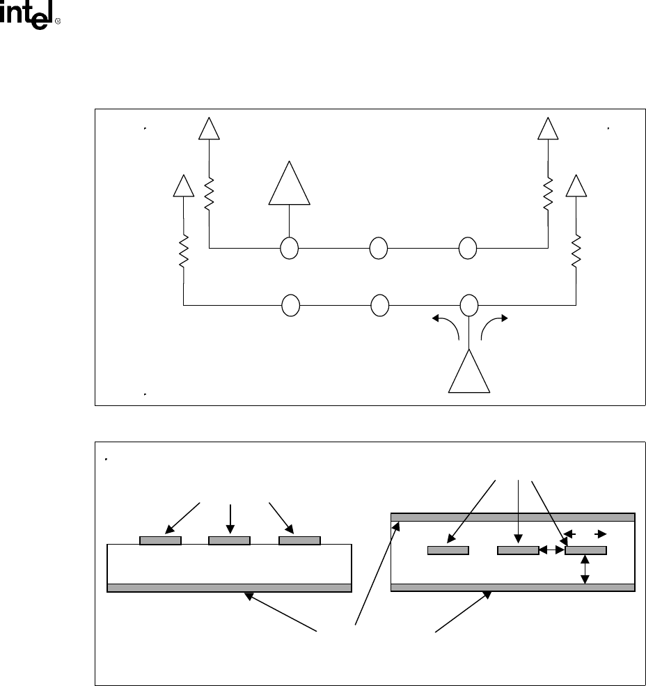
Intel®820 Chipset Design Guide 3-17
Advanced System Bus Design
Additional aggressors are possible in the z-direction, if adjacent signal layers are not routed in
mutually perpendicular directions. Because cross-talk-coupling coefficients decrease rapidly with
increasing separation, it is rarely necessary to consider aggressors that are at least five line widths
separated from the victim. The maximum cross-talk occurs when all the aggressors are switching in
the same direction at the same time.
There is cross-talk internal to the IC packages, which can also affect the signal quality.
Backward cross-talk is present in both stripline and microstrip geometry’s (see Figure 3-5). A way
to remember which geometry is stripline and which is microstrip is that a stripline geometry
requires stripping a layer away to see the signal lines. The backward coupled amplitude is
proportional to the backward cross-talk coefficient, the aggressor’s signal amplitude, and the
coupled length of the network up to a maximum that is dependent on the rise/fall time of the
aggressor’s signal. Backward cross-talk reaches a maximum (and remains constant) when the
Figure 3-4. Aggressor and Victim Networks
Figure 3-5. Transmission Line Geometry: (A) Microstrip (B) Stripline
Aggressor
Zo
Signal propagates in both
directions on aggressor line.
Zo
Victim Zo
Zo
AC Ground Plane
A. Microstrip B. Stripline
Dielectric, εr
Signal Lines
Signal Lines
Dielectric, εr
W
Sp t
li d

Advanced System Bus Design
3-18 Intel®820 Chipset Design Guide
propagation time on the coupled network length exceeds one half of the rise time of the aggressor’s
signal. Assuming the ideal ramp on the aggressor from 0% to 100% voltage swing, and the fall
time on an unloaded coupled network, then:
An example calculation follows when the fast corner fall time is 3 V/ns and board delay is
175 ps/inch (2.1 ns/foot):
Fall time = 1.5 V÷3 V/ns = 0.5 ns
Length for Max Backward Cross-talk
= ½ * 0.5 ns * 1000 ps/ns ÷175 ps/in
= 1.43 inches
Agents on the AGTL+ bus drive signals in each direction on the network. This causes backward
cross-talk from segments on two sides of a driver. The pulses from the backward cross-talk travel
toward each other and meet and add at certain moments and positions on the bus. This can cause
the voltage (noise) from cross-talk to double.
3.3.3.1 Potential Termination Cross-Talk Problems
The use of commonly used “pull-up” resistor networks for AGTL+ termination may not be
suitable. These networks have a common power or ground pin at the extreme end of the package,
shared by 13 to 19 resistors (for 14- and 20-pin components). These packages generally have too
much inductance to maintain the voltage/current needed at each resistive load. Intel recommends
using discrete resistors, resistor networks with separate power/ground pins for each resistor, or
working with a resistor network vendor to obtain resistor networks that have acceptable
characteristics.
LengthforMaxBackwardCrosstalk
1
2
---F×allTime
BoardDelayPerUnitLength
-------------------------------------------------------------------------=

Intel®820 Chipset Design Guide 3-19
Advanced System Bus Design
3.4 More Details and Insight
3.4.1 Textbook Timing Equations
The “textbook” equations used to calculate the propagation rate of a PCB are the basis for
spreadsheet calculations for timing margin based on the component parameters. These equations
are:
Equation 3-6. Intrinsic Impedance
(Ω)
Equation 3-7. Stripline Intrinsic Propagation Speed
(ns/ft)
Equation 3-8. Microstrip Intrinsic Propagation Speed
(ns/ft)
Equation 3-9. Effective Propagation Speed
(ns/ft)
Equation 3-10. Effective Impedance
(Ω)
Equation 3-11. Distributed Trace Capacitance
(pF/ft)
Equation 3-12. Distributed Trace Inductance
(nH/ft)
ZL
C
00
0
=
SSTRIPLINE r
01017
_.*=
ε
SMICROSTRIP r
01017 0 475 067
_.*.* .=+
ε
SEFF SCD
C
=∗+
01
0
ZEFF
Z
CD
C
=
+
0
1
0
CS
Z
00
0
=
LZ
S
012 00
=∗∗

Advanced System Bus Design
3-20 Intel®820 Chipset Design Guide
Symbols for Equation 3-5 through Equation 3-12:
•S0 is the speed of the signal on an unloaded PCB in ns/ft. This is referred to as the board
propagation constant.
•S0 MICROSTRIP and S0 STRIPLINE refer to the speed of the signal on an unloaded microstrip or
stripline trace on the PCB in ns/ft.
•Z0 is the intrinsic impedance of the line in Ω and is a function of the dielectric constant (εr), the
line width, line height and line space from the plane(s). The equations for Z0 are not included
in this document. See the MECL System Design Handbook by William R. Blood, Jr. for these
equations.
•C0 is the distributed trace capacitance of the network in pF/ft.
•L0 is the distributed trace inductance of the network in nH/ft.
•CD is the sum of the capacitance of all devices and stubs divided by the length of the network’s
trunk, not including the portion connecting the end agents to the termination resistors in pF/ft.
•SEFF and ZEFF are the effective propagation constant and impedance of the PCB when the
board is “loaded” with the components.
3.4.2 Effective Impedance and Tolerance/Variation
The impedance of the PCB needs to be controlled when the PCB is fabricated. The method of
specifying control of the impedance needs to be determined to best suit each situation. Using
stripline transmission lines (where the trace is between two reference planes) is likely to give better
results than microstrip (where the trace is on an external layer using an adjacent plane for reference
with solder mask and air on the other side of the trace). This is in part due to the difficulty of
precise control of the dielectric constant of the solder mask, and the difficulty in limiting the plated
thickness of microstrip conductors, which can substantially increase cross-talk.
The effective line impedance (ZEFF) is recommended to be 60 Ω ±15%, where ZEFF is defined by
Equation 3-10.
3.4.3 Power/Reference Planes, PCB Stackup, and High
Frequency Decoupling
3.4.3.1 Power Distribution
Designs using the Pentium III processor require several different voltages. The following
paragraphs describe some of the impact of two common methods used to distribute the required
voltages. Refer to the Flexible Motherboard Power Distribution Guidelines for more information
on power distribution.
The most conservative method of distributing these voltages is for each of them to have a dedicated
plane. If any of these planes are used as an “AC ground” reference for traces to control trace
impedance on the board, then the plane needs to be AC coupled to the system ground plane. This
method may require more total layers in the PCB than other methods. A 1-ounce/ft2 thick copper is
recommended for all power and reference planes.
A second method of power distribution is to use partial planes in the immediate area needing the
power, and to place these planes on a routing layer on an as-needed basis. These planes still need to
be decoupled to ground to ensure stable voltages for the components being supplied. This method
has the disadvantage of reducing area that can be used to route traces. These partial planes may also
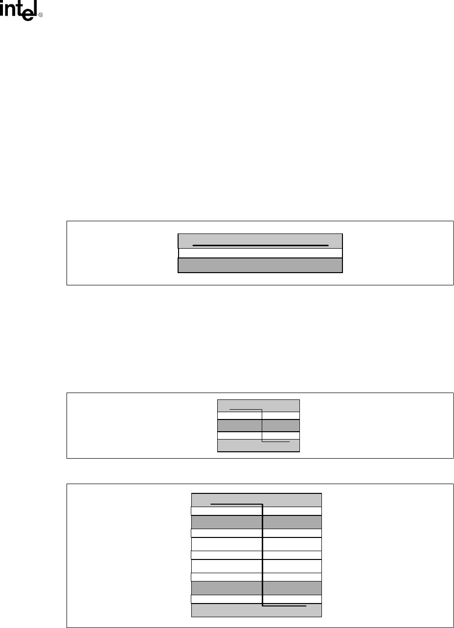
Intel®820 Chipset Design Guide 3-21
Advanced System Bus Design
change the impedance of adjacent trace layers. (For instance, the impedance calculations may have
been done for microstrip geometry, and adding a partial plane on the other side of the trace layer
may turn the microstrip into a stripline.)
3.4.3.2 Reference Planes and PCB Stackup
It is strongly recommended that baseboard stackup be arranged such that AGTL+ signals are
referenced to a ground (VSS) plane, and that the AGTL+ signals do not traverse multiple signal
layers. Deviating from either guideline can create discontinuities in the signal’s return path that can
lead to large SSO effects that degrade timing and noise margin. Designing an AGTL+ platform
incorporating discontinuities will expose the platform to a risk that is very hard to predict in pre-
layout simulation. Figure 3-6 shows the ideal case where a particular signal is routed entirely
within the same signal layer, with a ground layer as the single reference plane.
When it is not possible to route the entire AGTL+ signal on a single VSS referenced layer, there
are methods to reduce the effects of layer switches. The best alternative is to allow the signals to
change layers while staying referenced to the same plane (see Figure 3-7). Figure 3-8 shows
another method of minimizing layer switch discontinuities, but may be less effective than
Figure 3-7. In this case, the signal still references the same type of reference plane (ground). In
such a case, it is important to stitch (i.e., connect) the two ground planes together with vias in the
vicinity of the signal transition via.
Figure 3-6. One Signal Layer and One Reference Plane
Ground Plane
Signal Layer A
1lay 1ref plane vsd
Figure 3-7. Layer Switch with One Reference Plane
Figure 3-8. Layer Switch with Multiple Reference Planes (same type)
l1fld
Signal Layer A
Signal Layer B
Ground Plane
l M lt f l d
Signal Layer A
Signal Layer B
Layer
Layer
Ground Plane
Ground Plane
Advanced System Bus Design
3-22 Intel®820 Chipset Design Guide
When routing and stackup constraints require that an AGTL+ signal reference VCC or multiple
planes, special care must be given to minimize the SSO impact to timing and noise margin. The
best method of reducing adverse effects is to add high-frequency decoupling wherever the
transitions occur, as shown in Figure 3-9 and Figure 3-10. Such decoupling should, again, be in the
vicinity of the signal transition via and use capacitors with minimal effective series resistance
(ESR) and effective series inductance (ESL). When placing the caps it is recommended to space
the VSS and VCC vias as close as possible and/or use dual vias since the via inductance may
sometimes be higher than the actual capacitor inductance.
3.4.3.3 High Frequency Decoupling
This section contains several high frequency decoupling recommendations that will improve the
return path for an AGTL+ signal. These design recommendations will very likely reduce the
amount of SSO effects.
Just as layer switching and multiple reference planes can create discontinuities in an AGTL+ signal
return path, discontinuities may also occur when a signal transitions between the baseboard and
cartridge. Therefore, providing adequate high-frequency decoupling across VCCCORE and ground
at the SC242 connector interface on the baseboard will minimize the discontinuity in the signal’s
reference plane at this junction. Note that these additional high-frequency decoupling capacitors
are in addition to the high-frequency decoupling already on the processor.
Transmission line geometry also influences the return path of the reference plane. The following
are decoupling recommendations that take this into consideration:
•A signal that transitions from a stripline to another stripline should have close proximity
decoupling between all four reference planes.
•A signal that transitions from a stripline to a microstrip (or vice versa) should have close
proximity decoupling between the three reference planes.
•A signal that transitions from a stripline or microstrip through vias or pins to a component
(Intel 82820 MCH, etc.) should have close proximity decoupling across all involved reference
planes to ground for the device.
Figure 3-9. Layer Switch with Multiple Reference Planes
Figure 3-10. One Layer with Multiple Reference Planes
Signal Layer A
Ground Plane
Power Plane
Signal Layer B
Layer
Layer
1l M lt f l d
Ground
Signal Layer A
Power

Intel®820 Chipset Design Guide 3-23
Advanced System Bus Design
3.4.3.4 SC242 Connector
Intel studies indicate that the use of thermal reliefs on the connector pin layout pattern (especially
ground pins) should be minimized. Such reliefs (cartwheels or wagon-wheels) increase the net
ground inductance and reduce the integrity of the ground plane to which many signals are
referenced. Increased ground inductance has been shown to aggravate SSO effects. Also, the anti-
pad diameters (clearance holes in the planes) for the signal pins should be minimized since large
anti-pads also reduce the integrity of the ground plane and increase inductance.
Some additional layout and EMI-reduction guidelines regarding the SC242 connector follow:
•Extend power/ground planes up to the SC242 connector pins.
•Extend the reference planes for AGTL+ and other controlled-impedance signals up to the
SC242 connector pins.
•Minimize or remove thermal reliefs on power/ground pins.
•Route VTT power with the widest signal trace or mini-plane as possible. Place decoupling caps
across VTT and ground in the vicinity of the connector pins.
•Use a ground plane under the principal component side of the baseboard (and secondary side if
it contains active components).
•Distribute decoupling capacitors across power and ground pins evenly around the connector
(less than 0.5 inch spacing) on the primary and secondary sides.
•Minimize serpentine traces on outer layers.
3.4.4 Clock Routing
Analog simulations are required to ensure clock net signal quality and skew is acceptable. The
system clock skew must be kept to a minimum (The calculations and simulations for the example
topology given in this document have a total clock skew of 200 ps and 150 ps of clock jitter). For a
given design, the clock distribution system, including the clock components, must be evaluated to
ensure these same values are valid assumptions. Each processor’s datasheet specifies the clock
signal quality requirements. To help meet these specifications, follow these general guidelines:
•Tie clock driver outputs if clock buffer supports this mode of operation.
•Match the electrical length and type of traces on the PCB (microstrip and stripline may have
different propagation velocities).
•Maintain consistent impedance for the clock traces.
— Minimize the number of vias in each trace.
— Minimize the number of different trace layers used to route the clocks.
— Keep other traces away from clock traces.
•Lump the loads at the end of the trace if multiple components are to be supported by a single
clock output.
•Have equal loads at the end of each network.
The ideal way to route each clock trace is on the same single inner layer, next to a ground plane,
isolated from other traces, with the same total trace length, to the same type of single load, with an
equal length ground trace parallel to it, and driven by a zero skew clock driver. When deviations
from ideal are required, going from a single layer to a pair of layers adjacent to power/ground
planes would be a good compromise. The fewer number of layers the clocks are routed on, the
smaller the impedance difference between each trace is likely to be. Maintaining an equal length

Advanced System Bus Design
3-24 Intel®820 Chipset Design Guide
and parallel ground trace for the total length of each clock ensures a low inductance ground return
and produces the minimum current path loop area. (The parallel ground trace will have lower
inductance than the ground plane because of the mutual inductance of the current in the clock
trace.)
3.5 Definitions of Flight Time Measurements/
Corrections and Signal Quality
Acceptable signal quality must be maintained over all operating conditions to ensure reliable
operation. Signal Quality is defined by four parameters: Overshoot, Undershoot, Settling Limit,
and Ringback. Timings are measured at the pins of the driver and receiver, while signal integrity is
observed at the receiver chip pad. When signal integrity at the pad violates the following guidelines
and adjustments need to be made to flight time, the adjusted flight time obtained at the chip pad can
be assumed to have been observed at the package pin, usually with a small timing error penalty.
3.5.1 VREF Guardband
To account for noise sources that may affect the way an AGTL+ signal becomes valid at a receiver,
VREF is shifted by ∆VREF for measuring minimum and maximum flight times. The VREF
Guardband region is bounded by VREF-∆VREF and VREF+∆VREF. ∆VREF has a value of 100 mV,
which accounts for the following noise sources:
•Motherboard coupling
•VTT noise
•VREF noise
3.5.2 Ringback Levels
The example topology covered in this guideline assumes ringback tolerance allowed to within
200 mV of 2/3 VTT. Since VTT is specified with approximate total ±11% tolerance, this implies a
2/3 VTT (VREF) range from approximately 0.89 V to 1.11 V. This places the absolute ringback
limits at:
•1.3 V (1.1 V + 200 mV) for rising edge ringback
•0.69 V (0.89 V – 200 mV) for falling edge ringback
A violation of these ringback limits requires flight time correction as documented in the Intel®
Pentium® II Processor Developer’s Manual.
3.5.3 Overdrive Region
The overdrive region is the voltage range, at a receiver, from VREF to VREF + 200 mV for a low-to-
high going signal and VREF to VREF - 200 mV for a high-to-low going signal. The overdrive
regions encompass the VREF Guardband. So, when VREF is shifted by ∆VREF for timing
measurements, the overdrive region does not shift by ∆VREF. Figure 3-11 depicts this relationship.
Corrections for edge rate and ringback are documented in the Intel® Pentium® II Processor
Developer’s Manual. However, there is an exception to the documented correction method. The
Intel®Pentium® II Processor Developer’s Manual states that extrapolations should be made from
the last crossing of the overdrive region back to VREF. Simulations performed on this topology
Intel®820 Chipset Design Guide 3-25
Advanced System Bus Design
should extrapolate back to the appropriate VREF Guardband boundary, and not VREF. So, for
maximum rising edge correction, extrapolate back to VREF + ∆VREF. For maximum falling edge
corrections, extrapolate back to VREF - ∆VREF.
3.5.4 Flight Time Definition and Measurement
Timing measurements consist of minimum and maximum flight times to take into account that
devices can turn on or off anywhere in a VREF Guardband region. This region is bounded by
VREF-∆VREF and VREF+∆VREF. The minimum flight time for a rising edge is measured from the
time the driver crosses VREF when terminated to a test load, to the time when the signal first
crosses VREF-∆VREF at the receiver (see Figure 3-12). Maximum flight time is measured to the
point where the signal first crosses VREF+∆VREF, assuming that ringback, edge rate, and
monotonicity criteria are met. Similarly, minimum flight time measurements for a falling edge are
taken at the VREF+∆VREF crossing and maximum flight time is taken at the VREF-∆VREF crossing.
Figure 3-11. Overdrive Region and VREF Guardband
V
REF
+ 200 mV
∆
∆∆
∆
∆
∆∆
∆
V
REF
+ 100 mV
V
REF
V
REF
- 100 mV
V
REF
- 200 mV
V
REF
V
REF
V
REF
Guardband
Overdrive Region (200 mV)
Overdrive Region (200 mV)
Figure 3-12. Rising Edge Flight Time Measurement
Overdrive Regio
V
REF
Guardband
Driver Pin into
Test Load
Receiver Pin
Tflight-min
Tflight-max
V
REF
+ 200 mV
V
REF
+ 100 mV
V
REF
V
REF
- 100 mV
∆
V
REF
∆
V
REF

Advanced System Bus Design
3-26 Intel®820 Chipset Design Guide
3.6 Conclusion
AGTL+ routing requires a significant amount of effort. Planning ahead and leaving the necessary
time available for correctly designing a board layout will provide the designer with the best chance
of avoiding the more difficult task of debugging inconsistent failures caused by poor signal
integrity. Intel recommends planning a layout schedule that allows time for each of the tasks
outlined in this document.

4
Clocking
This page is intentionally left blank.

Intel®820 Chipset Design Guide 4-1
Clocking
Clocking 4
4.1 Clock Generation
There are two clock generator components required in an Intel® 820 chipset based system. The
Direct Rambus* Clock Generator (DRCG) generates clock for the Direct Rambus* interface while
the CK133 component generates clocks for the rest of the system. Clock synthesizers that meet the
Intel CK98 Clock Specification are suitable for an Intel® 820 chipset based system. The CK133
generates the clocks listed in Table 4-1.
The CK133 is a mixed voltage component. Some of the output clocks are 3.3V and some of the
output clock are 2.5V. As a result, the CK133 device requires both 3.3V and 2.5V. These power
supplies should be a clean as possible. Noise in the power delivery system for the clock driver can
cause noise on the clock lines.
The MCH uses the same clock for hub interface and AGP. It is important that the
hub interface/AGP clocks are routed to ensure the skew requirements are met between:
•The MCH hub interface/AGP clock and the AGP connector (or device)
Table 4-1. Intel® 820 Chipset Platform System Clocks
Number Name on
CK133 Used for Routed to Name on
Receiver Frequency Voltage
4 CPUCLK[0-3] System Bus Clock
2 Processors CLK
100/133 MHz 2.5VMCH HCLKIN
ITP BCLK
3 APIC[0-2] APIC Bus Clock 2 Processors PICCLK 33 MHz 2.5V
ICH APICCLK
8 PCICLK[1-7,F]
PCI Bus Clock 5 PCI
Devices CLK
33 MHz 3.3V
PCI, LPC, FWH Flash
BIOS Bus Clock ICH PCICLK
FWH Flash BIOS
Interface Clock FWH Flash
BIOS CLK
LPC Interface Clock LPC CLK
4 3V66[0-3]
Hub Interface/AGP Bus
Clock MCH CLK66
66 MHz 3.3V
Hub Interface Clock ICH CLK66
AGP Bus Clock AGP device/
slot CLK
Unused N/A N/A
2REF[0-1]
Internal ICH Logic ICH CLK14
14 MHz 3.3V
Internal Super I/O Logic Super I/O Vendor
Specific
1 48 MHz USB ICH CLK48 48 MHz 3.3V
2 CPU_DIV2[0-1] DRCG Reference Clock DRCG REFCLK 50/66 MHz 2.5V
Unused N/A N/A
Clocking
4-2 Intel®820 Chipset Design Guide
•The MCH hub interface/AGP clock and the ICH hub interface clock.
The DRCG reference clock operates at one-half the CPU clock frequency. It is an input into the
DRCG and is used to generate the Direct RDRAM “Clock to Master” differential pair (CTM,
CTM#).
The DRCG generates one pair of differential Direct RDRAM Clocks (CTM, CTM#) from the
reference clock generated by the CK133. In addition, the DRCG uses phase information provided
by the MCH to phase align the direct RDRAM clock with the CPU clocks. This phase alignment
information is provided to the DRCG via the SYNCLKN and PCLKM pins.
Figure 4-1. Intel® 820 Chipset Platform Clock Distribution
CPUCLK
APIC
PCICLK*
REF
48Hz
Processor
CLK
PICCLK
Processor
CLK
PICCLK
CPUCLK
APIC
MCH
CPUCLK
HCLKIN
3V66
CLK66
RDRAM RDRAMRDRAM
CTM
CFM
RCLK TCLK RCLKRCLK TCLK TCLK
PHASEINFO PHASEINFO
DRCG
TERM
ICH
APIC
CPU_DIV2 REFCLK
3V66 CLK
AGP
CONNECTOR
APICCLK
PCICLK
3V66
CLK66
CLK14
CLK48
FWH
Flash BIOS
PCICLK
CLK
CLK
LPC
PCICLK
P
M
N
E
D
C
B
A
H
G
F
J
I
K
PCI SLOTS
PCI SLOTS
PCI SLOTS
PCICLK
CLK
CLK
CLK
L
L
L
CK133
Q
PCI SLOTS
CLK
L
RDRAM
RCLK TCLK
* The free-running PCI clock should be connected to the ICH.

Intel®820 Chipset Design Guide 4-3
Clocking
NOTES:
1. DP Only
2. UP: MCH and CPU clock drivers are tied together to eliminate pin-to-pin skew. –175 and +175 pin-to-pin
skew only apply to DP.
3. UP Only
4. Clock drivers tied together to eliminate pin-to-pin skew.
5. The skew between any PCICLK clocks on any two inputs in the system.
6. The skew between any APIC clocks on any two inputs in the system.
7. If SSC is enabled, an additional ±40ps must is added to the pin-to-pin skew
8. If SSC is enabled, an additional ±60ps must is added to the pin-to-pin skew
Table 4-2. Intel® 820 Chipset Platform Clock Skews
Clock Symbols
See Figure 4-1 Relationship
Skew
Notes
Pin-to-Pin
(ps) Board
(ps) Total
(ps)
MinMaxMinMaxMinMax
A leads C,
A leads E
(or C leads E)
SC242 HCLK to SC242
HCLK (DP ONLY)
And
SC242 HCLK to MCH
HCLK (DP ONLY)
-175 +175 -125 +125 -300 +300 1, 7
A leads E SC242 HCLK to MCH
HCLK (UP ONLY) 0 0 -125 +125 -125 +125 2, 3, 7
P leads F MCH CLK66 to AGP
graphics device
AGPCLK 0 0 -125 +125 -125 +125 4, 8
L leads another L
(or L leads H) PCICLK to PCICLK -500 +500 -1500 +1500 -2000 +2000
I leads H ICH CLK66 leads ICH
PCICLK +1500 +4000 -500 +500 +1000 +4500
F leads I ICH CLK66 to MCH
CLK66 -250 250 -125 +125 -375 +375 8
Worst case skew
between H, L, M
and N
Worst case FWHCLK,
LPCCLK, PCICLK -500 +500 -1500 +1500 -2000 +2000 5
B leads D,
B leads G
Processor PICCLK leads
Processor PICCLK
And
Processor PICCLK leads
ICH APICCLK
-250 +250 -125 +125 -375 +375 6
Clocking
4-4 Intel®820 Chipset Design Guide
Figure 4-2 shows the Intel® 820 chipset clock length routing guidelines.
Figure 4-2. Intel® 820 Chipset Clock Routing Guidelines1,2
Note:
1. Tie 3V66 clock for the MCH to 3V66 clock for the AGP connector to eliminate pin-to-pin skew.
2. These calculations based on 150ps/in trace velocity.
3. The TBD value will be derived from the PCI Revision 2.2 Specification which allows for a maximum of ±2ns
clock skew.
CPUCLK to MCH
Y
CPUCLK to SC242
Note: Tie CPUCLK for the MCH to CPUCLK to the SC242 to eliminate pin-to-pin skew.
±0"
Y5.3"
3V66 Clock for
MCH and ICH ±0"
4"Z
PCI Clock for ICH ±0"
4"Z
PCI Clock for On-Board
Devices (excluding ICH) ±TBD
3
4"Z
3V66 Clock for
AGP Slot
Z
PCI Clock for
PCI Slots ±TBD
3
1.5"Z
820 lk t d
Intel®820 Chipset Design Guide 4-5
Clocking
NOTES:
1. Differential Clocking Pair
2. CFM/CFM# driven by MCH
Table 4-3. Intel® 820 Chipset Platform System Clock Cross-Reference
CK133/DRCG Pin Name Component Pin Name
PCICLK
PCI Slot CLK
PCI Slot CLK
PCI Slot CLK
PCI Slot CLK
PCI Slot CLK
ICH PCICLK-F
LPC Super I/O CLK
FWH Flash BIOS CLK
3V66
MCH GCLKIN
ICH CLK66
AGP Connector (on-board device) CLK
48 MHz ICH CLK48
CPUCLK
CPU BCLK
CPU BCLK
MCH HCLKIN
CPU_div2 DRCG Refclk
APIC
CPU PICCLK
CPU PICCLK
ICH APICCLK
Clk/ClkB1RDRAMs
MCH CTM/CTM#
CFM/CFM#1,2 RDRAMs
PclkM MCH HCLKOUT
SynclkN MCH RCLKOUT
Clocking
4-6 Intel®820 Chipset Design Guide
4.2 Component Placement and Interconnection Layout
Requirements
Detailed explanation of layout requirements for each interconnections are provided in the
following sections:
•Crystal to CK133
•CK133 to DRCG
•MCH to DRCG
•DRCG to RDRAM channel
4.2.1 14.318 MHz Crystal to CK133
The distance between the crystal and the CK133 should be minimized. The maximum trace length
is 500 mils.
4.2.2 CK133 to DRCG
•CPU_div2
•VDDIR – Used as a reference for 2.5V signaling
VddIR and CPU_div2 must be routed as shown in Figure 4-3. Note that the VddiR pin can be
connected directly to 2.5V near the DRCG if the 2.5V plane extends near the DRCG. However, if a
2.5V trace must be used, it should originate at the CK133 and be routed as shown.
Figure 4-3. CK133 to DRCG Routing Diagram
Ground
Ground/Power Plane
6 mils
4.5 mils
1.4 mils
1.4 mils
6 mils
VddiR
6 mils
6 mils
Ground
6 mils
6 mils CPU_div2
6 mils
6 mils
Ground
6 mils
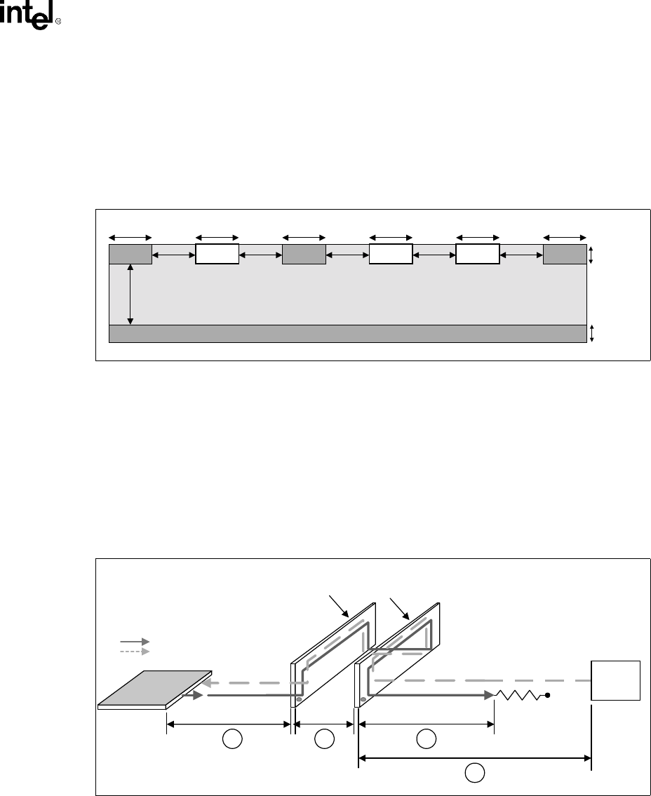
Intel®820 Chipset Design Guide 4-7
Clocking
4.2.3 MCH to DRCG
•PclkM
•PclkN
•VddIPD
The Hclkout, Rclkout and VddiPD should be routed as shown in Figure 4-4. Note that the VddiPD
pin can be connected directly to 1.8V near the DRCG if the 1.8V plane extends near the DRCG.
However, if a 1.8V trace must be run, it should originate at the MCH and be routed as shown.
The maximum length for Hclkout and Rclkout is 6”. Additionally, Hclkout and Rclkout must be
length matched (to each other) within 50 mils. These signals should be routed on the same layer. If
the signals must switch layers, then BOTH signals should change layers together.
If VddiPD is connected to the 1.8V plane using a via (e.g., a trace is not run from the MCH),
Hclkout and Rclkout must still be routed differentially and ground isolated.
Figure 4-4. MCH to DRCG Routing Diagram
Ground
Ground/Power Plane
6 mils
4.5 mils
1.4 mils
1.4 mils
6 mils
VddiPD
6 mils
6 mils
Ground
6 mils
6 mils
Hclkout
6 mils
6 mils
Rclkout
6 mils
6 mils
Ground
6 mils
Figure 4-5. Direct Rambus* Clock Routing Dimensions
blkt
MCH
RIMM_0 RIMM_1
A B C
0"-3.50" 0.4"-0.45" 0"-3"
DRCG
D
(A) = CTM/CTM# RIMM to MCH
(A) = CFM/CFM# MCH to RIMM
(B) = RIMM to RIMM for Clocks
(C) = RIMM to Termination
(D) = DRCG to RIMM
CFM/CFM#
CTM/CTM#
0"-6"
Term
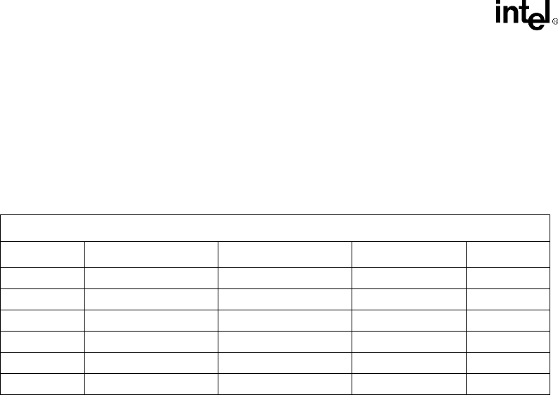
Clocking
4-8 Intel®820 Chipset Design Guide
4.2.4 DRCG to RDRAM Channel
The Direct Rambus* clock signals (CTM/CTM# and CFM/CFM#) are high-speed, impedance
matched transmission lines. The Direct Rambus* clocks begin at the end of the Direct Rambus*
channel and propagate to the controller as CTM/CTM# (see Figure 4-5), where it loops back as
CFM/CFM#. Table 4-4 lists the placement guidelines.
NOTE: * Refer to Figure 4-5
Trace Geometry
In Sections labeled ‘A’ and ‘D’ (Figure 4-5) the clock signals (CTM/CTM# and CFM/CFM#) must
be 14 mils wide and routed as shown in Figure 4-6. For all other sections (‘B’ and ‘C’) the clock
signals must be routed with 18 mil wide traces. There must be a 22 mil ground isolation trace
routed around the clock differential pair signals. The 22 mil ground isolation traces must be
connected to ground with a via every 1”. A 6 mil gap is required between the clock signals and the
ground isolation traces. For the section labeled “A” in Figure 4-5, 0.021 inches of CLK per 1 inch
of RSL trace length must be added to compensate for the clocks faster trace velocity as described in
Section 2.6.2.1, “RSL Routing” on page 2-8. The CTM/CTM# and the CFM/CFM# differential
signal pairs must be length matched to ±2 mils in line section labeled ‘A’ and for the line sections
labeled ‘B’ using the trace length methods in Section 2.6.2.1, “RSL Routing” on page 2-8. For the
section labeled ‘D’ the trace length matching for CTM/CTM# is ±2 mils, and for the section
labeled ‘C’, ±2 mil trace length matching is required for the CFM/CFM# signals.
The CTM/CTM# signals must be ground referenced (with a continuous ground island/plane) from
the DRCG to the Last RIMM.
4.2.5 Trace Length
For the section labeled “A” in Figure 4-5 (1st RIMM to MCH and MCH to 1st RIMM),
CTM/CTM# and CFM/CFM# must be length matched within ±2 mils (exact trace length matching
is recommended). Package trace compensation (as described in Section 2.6.2.1, “RSL Routing”
on page 2-8), via compensation, and RSL signal layer alternation must also be completed on
the clock signals. Additionally, 0.021 inches of CLK per 1 inch of RSL trace length must be added
to compensate for the clocks faster trace velocity as described in Section 2.6.2.1.
For the line sections labeled ‘B’ (Figure 4-5) (RIMM to RIMM) the clock signals must be matched
within ±2 mils to the trace length of every RSL signal. Exact length matching is preferred.
Table 4-4. Placement Guidelines for Motherboard Routing Lengths
Direct Rambus* Clock Routing Length Guidelines
Clock From To Length (inches) Section*
CTM/CTM# DRCG Last RIMM Connector 0.000 – 6.000 D
RIMM RIMM 0.400 – 0.450 B
1st RIMM Connector Chipset 0.000 – 3.500 A
CFM/CFM# Chipset 1st RIMM Connector 0.000 – 3.500 A
RIMM RIMM 0.400 – 0.450 B
Last RIMM Connector Termination 0.000 – 3.000 C
Intel®820 Chipset Design Guide 4-9
Clocking
For the line section labeled ‘D’ (DRCG to Last RIMM) the CTM/CTM# must be length matched
within ±2 mils (exactly is recommended), and for the section labeled ‘C’, ±2 mil trace length
matching is required for the CFM/CFM# signals.
Note: Total trace length matching for the entire CTM/CTM# signal trace (Sections A+B+D) and for the
CFM/CFM# signal trace (Sections A+B) is ±2 mils (exact length matching is recommended).
The CFM/CFM# differential pair signals require termination using either 27 Ω 1% or 28 Ω 2%
resistors and a 0.1 uF capacitor as shown in Figure 4-8.
Figure 4-6. Differential Clock Routing Diagram (Section ‘A’, ‘C’, & ‘D’)
Figure 4-7. Non-Differential Clock Routing Diagram (Section ‘B’)
Ground CLOCK CLOCK# Ground
Ground/Power Plane
22 mils 22 mils14 mils 14 mils
6 mils 6 mils6 mils
4.5 mils 4.5 mils
2.1 mils
1.4 mils
dif lk t d
Ground CLOCK/CLOCK# Ground
Ground/Power Plane
10 mils 10 mils18 mils
6 mils 6 mils
4.5 mils 4.5 mils
2.1 mils
1.4 mils
Figure 4-8. Termination for Direct Rambus* Clocking Signals CFM/CFM#
R1
CFM
CFM#
R2
28
Ω
2%
or
27
Ω
1%
C1
0 .1 uF
28
Ω
2%
or
27
Ω
1%
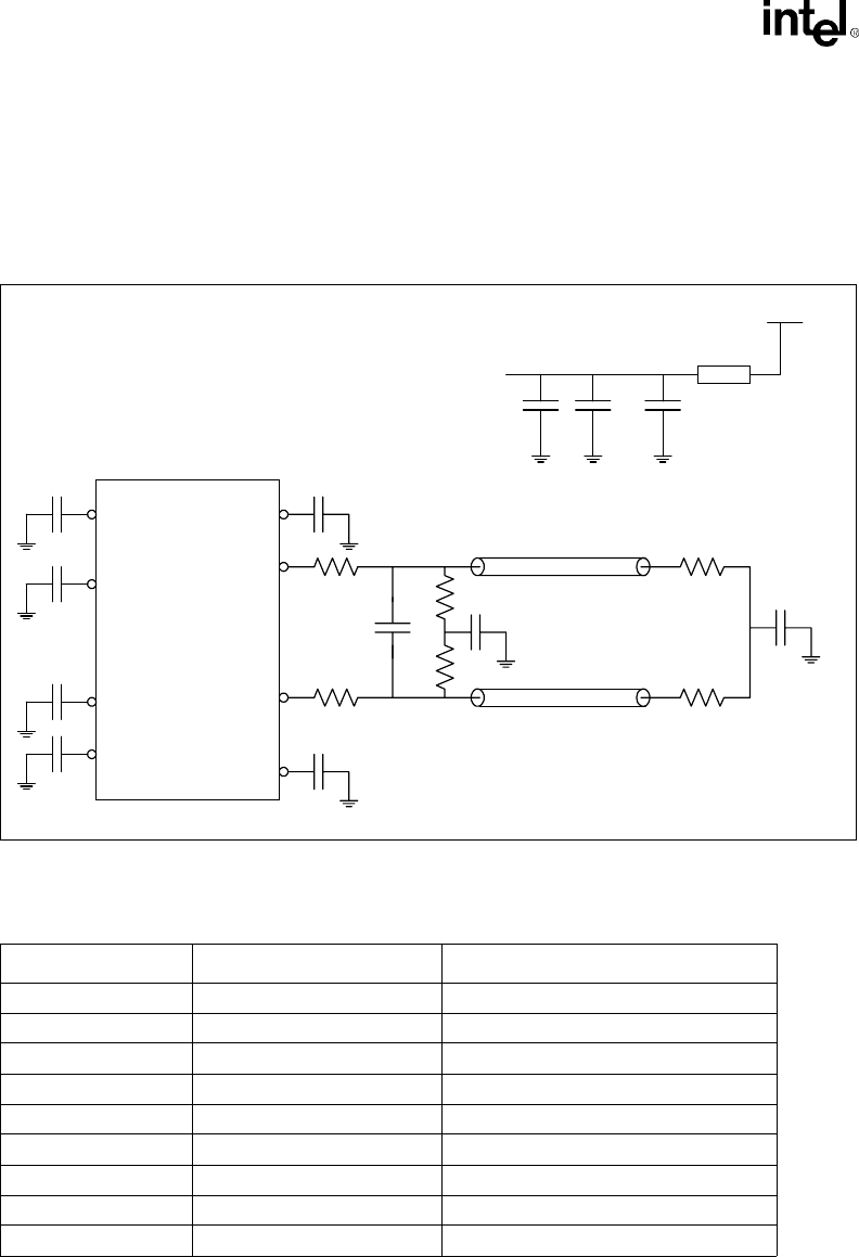
Clocking
4-10 Intel®820 Chipset Design Guide
4.3 DRCG Impedance Matching Circuit
The external DRCG impedance matching circuit is shown in Figure 4-9. The values for the
elements are listed in Table 4-5.
NOTES:
1. The ferrite bead and 10 uF bulk cap combination improves jitter and helps to keep the clock noise away from
the rest of the system.
2. 0.1 uF capacitors are better than 0.01 uF or 0.001 uF caps for DRCG decoupling.
The circuit shown in Figure 4-9 is required to match the impedance of the DRCG to the 28 Ω
channel impedance. More detailed information can be found in the Direct Rambus Clock Generator
Specification.
Figure 4-9. DRCG Impedance Matching Network
DRCG
CD
RSRP
RT
Z
CH
CF
VDD VDDO
VDD
O
CD
RS
CMID
RPZ
CH
C
MID2
RT
IR
VDD P
VDD
VDD
C
IPD
CD
CD
CD
CD
3.3v
FBead
CBulkCD2
CD2
To 3.3V DRCG
Supply Connection
Table 4-5. External DRCG Component Values1,2
Component Nominal Value Notes
CD0.1 uF Decoupling caps to ground
RS39 Ohms Series termination resistor
RP51 Ohms Parallel termination resistor
CMID, CMID2 0.1 uF Virtual ground caps
RT27 Ohms End of channel termination
CF4 pF Do not stuff
FBead 50 Ohms at 100 MHz Ferrite bead
CD2 0.1 uF Additional 3.3V decoupling caps
CBulk 10 uF Bulk cap on device side of ferrite bead
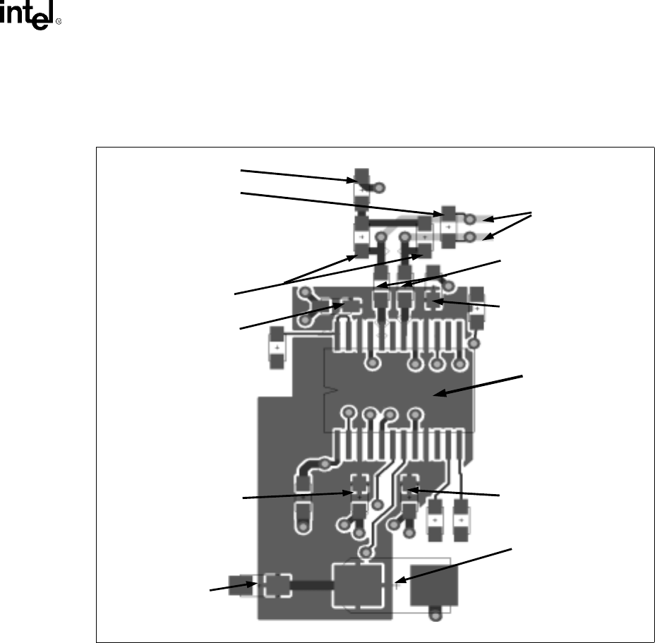
Intel®820 Chipset Design Guide 4-11
Clocking
4.3.1 DRCG Layout Example
4.4 AGP Clock Routing Guidelines
The AGP clock must be routed with 20 mil spacing to all other signals and it must meet the length
guidelines in Figure 4-2.
4.5 Series Termination Resistors for CK133 Clock
Outputs
All used outputs require series termination resistors. The recommended resistor value will be
defined by simulations. The stub length to the CK133 of these resistors can be compromised to
make room for decoupling caps. The rule is to keep all resistor stubs within 250 mils of the CK133.
If routing rules allow, Rpacks can be used if power dissipation is not exceeded for the Rpack.
Figure 4-10. DRCG Layout Example
Rs - 39Ω
(Keep trace from DRCG to
Rs VERY short)
Rp - 51Ω
(Keep trace from Rs
to Rp short)
CTM/CTM# route on
bottom layer
Cmid - 100pF
EMI Cap - 4pF
Do Not Stuff
Decoupling Cap - 0.1uF
(Place VERY Near DRCG 3.3V Pin!)
Decoupling Cap - 0.1uF
(Place VERY Near DRCG 3.3V Pin!)
Decoupling Cap - 0.1uF
(Place VERY Near DRCG 3.3V Pin!)
Decoupling Cap - 0.1uF
(Place VERY Near DRCG 3.3V Pin!)
Bulk Decoupling Cap - 10uF
(Place Near DRCG)
Ferrite Bead
(L22 in Reference Schematics)
3.3V-DRCG Flood
Flood 3.3V-DRCG on the top layer
around DRCG. Flood MUST include:
4 DRCG Power Pins
4 0.1uF Capacitors
1 10uF Bulk Capacitor
1 Isolation Ferrite Bead
Clocking
4-12 Intel®820 Chipset Design Guide
4.6 Unused Outputs
All unused clock outputs must be tied to ground through a series resistor approximately the
impedance of the output buffer (shown below.) The intent of these resistors is to terminate the
unused outputs to eliminate EMI.
4.7 Decoupling Recommendation for CK133 and DRCG
Some CK133 vendors may integrate the XTAL_IN and XTAL_OUT frequency adjust capacitors.
However, pads should be placed on the board for these external capacitors for testing/debug.
To further reduce jitter and voltage supply noise, the addition of a ferrite filter with 2 caps (10 uF
and 0.1 uF) on both the 2.5V and 3.3V planes close to the clock devices is recommended. This
applies to both DRCG and CK133.
4.8 DRCG Frequency Selection and the DRCG+
4.8.1 DRCG Frequency Selection Table and Jitter Specification
To allow additional flexibility in board design, Intel has enabled a variation of the DRCG labeled
the DRCG+. The device has the same specifications, pinout and form-factor as the existing DRCG
device document. There are two modifications made to the DRCG+.
1. The DRCG+ Mult[0:1] select table has changed to modify two of the multiplier ratios. The
DRCG+ will support 133/356 MHz using 66 MHZ DRCG+ input clock and a 16/3 multiplier.
An additional 9/2 multiplier allows 133/300 MHz (not supported by the Intel® 820 chipset).
Support for 300 MHz and 400 MHz memory bus is unchanged. The following table lists the
DRCG Ratio.
Table 4-6. Unused Output Termination
Buffer Name VCC Range (V) Impedance
(Ohms) If Unused Output
Termination to VSS
CPU, CPU_Div2, IOAPIC 2.375 - 2.625 13.5 - 45 30 Ohms
48 MHz, REF 3.135 - 3.465 20 - 60 40 Ohms
PCI, 3V66 3.135 - 3.465 12 - 55 33 Ohms
Table 4-7. DRCG Ratio
Mult[0:1] DRCG DRCG+
0:0 4:1 9:2
0:1 6:1 6:1
1:0 8:3 16:3
1:1 8:1 8:1
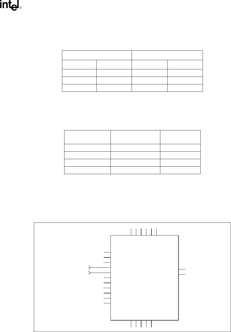
Intel®820 Chipset Design Guide 4-13
Clocking
2. The Intel® 820 chipset supports the following ratios and can be supported by the DRCG and
DRCG+ or derivative devices. Contact your DRCG vendor for information on DRCG,
DRCG+, and derivative products.
3. The jitter timing specifications are expanded to encompass both the component specification
(for DRCG or derivative products) and the channel specification. Follow the component
specification when measuring jitter at the DRCG output resistor. Follow the channel jitter
guidelines when measuring jitter at the MCH or at the termination for CFM/CFM# on the
RDRAM interface.
4.8.2 DRCG+ Frequency Selection Schematic
DRCG+ frequency selection can be accomplished using two GPIOs connected to the MULT[0:1]
pins as shown in Figure 4-11. This allows selection of all frequencies supported by the Intel® 820
chipset.
100 MHz Host Bus 133 MHz Host Bus
Frequency Multiplier Frequency Multiplier
100 / 300 6:1 133 / 266 4:1
100 / 400 8:1 133 / 356 16:3
133 / 400 6:1
Output Frequency
(MHz) Component Jitter
Specification Channel Jitter
Guidelines
400 50 ps 100 ps
356 60 ps 110 ps
300 70 ps 120 ps
266 80 ps 130 ps
Figure 4-11. DRCG+ Frequency Selection
REFCLK
PWRD#
STOPB#
MULTO
MULT1
S0
S1
GND
PCLKM
SYNCLKN
NC
2
12
11
15
14
24
23
13
6
7
19
GPO1
GPO2
17
21
4
8
5
GNDO1
GNDO2
GNDP
GNDC
GNDI
CLK
CLKB#
20
18
1
10
16
22
3
9
VDDIR
VDDIPD
VDDO1
VDDO2
VDDP
VDDC
U?
DRCG

Clocking
4-14 Intel®820 Chipset Design Guide
This page is intentionally left blank.

5
System
Manufacturing
This page is intentionally left blank.

Intel®820 Chipset Design Guide 5-1
System Manufacturing
System Manufacturing 5
5.1 In Circuit FWH Flash BIOS Programming
All cycles destined for the FWH Flash BIOS appear on PCI. The ICH hub interface to PCI Bridge
puts all processor boot cycles out on PCI (before sending them out on the FWH Flash BIOS
interface to the FWH Flash BIOS). If the ICH is set for subtractive decode, these boot cycles can be
accepted by a positive decode agent out on PCI. The enables the ability to boot from of a PCI card
that positively decodes these memory cycles. To boot from a PCI card it is necessary to keep the
ICH in subtractive decode mode. If a PCI boot card is inserted and the ICH is programmed for
positive decode, there will be two devices positively decoding the same cycle. In systems with the
82380AB (ISA bridge), it is also necessary to keep the NOGO signal asserted when booting from a
PCI ROM. Note that it is not possible to boot from a ROM behind the 82380AB. Once you have
booted from the PCI card, you could potentially program the FWH Flash BIOS in circuit and
program the ICH CMOS.
5.2 FWH Flash BIOS Vpp Design Guidelines
The Vpp pin on the FWH Flash BIOS is used for programming the flash cells. The FWH Flash
BIOS supports Vpp of 3.3V or 12V. If Vpp is 12V, the flash cells will program about 50% faster
than at 3.3V. However, the FWH Flash BIOS only supports 12V Vpp for 80 hours. The 12V Vpp
would be useful in a programmer environment that is typically an event that occurs very
infrequently (much less than 80 hours). The VPP pin MUST be tied to 3.3V on the motherboard.
5.3 Stackup Requirement
5.3.1 Overview
The Intel® 820 chipset platform requires a board stackup with a 4.5 mil prepreg. This change in
dimension (previously, typically 7 mil) is required because of the signaling environment used for
Direct RDRAM, AGP 2.0 and hub interface. The RDRAM Channel is designed for 28 Ω and
mismatched impedance will cause signal reflections which will reduce voltage and timing margins.
For example, with a 2X clock at 400 MHz operation, which equals a 1.25 ns sampling window,
only 100 ps is allotted for total channel timing error. Channel error results not only from PCB
impedance, but also PCB and Z0 process variation. Therefore, it is critical to attain the required
28 Ω impedance.
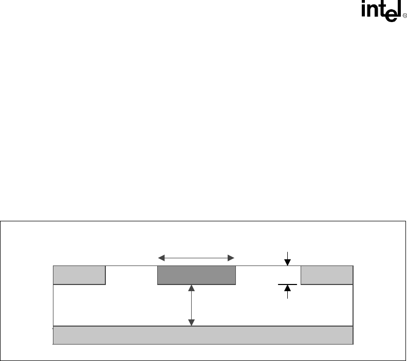
System Manufacturing
5-2 Intel®820 Chipset Design Guide
5.3.2 PCB Materials
PCB tolerances determine Z0 variation. Those tolerances include trace width, pre-preg thickness,
plating thickness, and dielectric constant. Pre-preg type impacts H tolerance and εr including single
ply, 2-ply, and resin content.
To design to the correct Z0 variation, PCB’s typically need to meet the following (see Table 5-2):
•Height tolerance ±10% (~ 0.4 mil)
•Width tolerance ±2.5% (~ 0.4 mil)
•εr tolerance ±5% (~0.2)
Stackup Requirement: 28Ω ±10%
5.3.3 Design Process
To meet the tight tolerances required a good design process to use is:
•Specify the material to be used
•Calculate board geometries for the desired impedance - or use the example stackup provided
•Build test boards and coupons
•Measure board impedance using a TDR and follow Intel’s Impedance Test Methodology
Document (found on developer.intel.com)
•Measure geometries with cross-section
•Adjust design parameters and/or material as required
•Build a new board, re-measure the key parameters and be prepared to generate one or two
board iterations
This process will require iteration: design, build, test, modify, build, test…
Figure 5-1. 28Ω Trace Geometry
H
W
ST
ε
εε
ε

Intel®820 Chipset Design Guide 5-3
System Manufacturing
5.3.4 Test Coupon Design Guidelines
Characterization and understanding of the trace impedance is critical for delivering reliable
systems at the increased bus frequencies. Incorporating a test coupon design into the motherboard
makes testing simpler and more accurate. The test coupon pattern must match the probe type being
used.
The location of the test coupon is listed in order of preference below:
•1st Choice (Ideal Location) = Memory section of the motherboard
•2nd Choice = Any section of the motherboard
•3rd Choice = Separate location in the panel
The Intel Impedance Test Methodology Document should be used to ensure boards are within the
28Ω ±10% requirement. The Intel Controlled Impedance Design and Test Document should be
used for the test coupon design and implementation. These documents can be found at:
http://developer.intel.com/design/chipsets/memory/rdram.htm
— Select “Application Notes”
5.3.5 Recommended Stackup
Though numerous variations of stackup are possible, it is recommended that the following should
be used as a starting point:
W=18 mil, H=4.5 mil, T=2.0, 1 ply 2116 pre-preg
For other possibilities see Table 5-1 and following figures:
5.3.6 Inner Layer Routing
Inner Layer Routing also has many possible stackups. For Inner Layer Routing, it is recommended
to use the following as a starting point:
W=13.5 mil, H1=7 mil, H2=5, T=1.2
With these parameters, initial TDR should fall within acceptable limits - 28 Ω ±10%
Figure 5-2 shows examples of both Stripline and Microstrip cross sections.
Table 5-1. 28Ω Stackup Examples
Sample Zo H W T SM(max) Resin %
1 27.1 4.3 18.0 2.1 0.6 53.0
2 28.1 3.8 18.5 1.6 1.2 72.0
3 28.6 4.8 19.0 2.5 0.7 61.0
System Manufacturing
5-4 Intel®820 Chipset Design Guide
Note: Don’t forget ground floods and stitching
5.3.7 Impedance Calculation Tools
The 3D Field Solvers (e.g., those by HP, Ansoft, Sonnet, and Polar) are the most accurate for
calculating impedance. Z calculators based on equations (zcalc) are also fairly accurate. The
differences are shown in Table 5-2.
5.3.8 Testing Board Impedance
The Intel Impedance Test Methodology Document should be used to ensure boards are within the
28 Ω ±10% requirement. This document can be found at: http://developer.intel.com.
Figure 5-2. (a,b) Microstrip and Stripline Cross-section for 28 Ω Trace
GG
4.5 mils
2.1 mils
6 mils 18 mils
10 mils
S
a) Microstrip Cross-Section for 28 Ohm trace
b) Stripline Cross-Section for 28 Ohm trace
GG
5 mils
1.2 mils
5 mils
13.5 mils
6 mils
S
7 mils
1.2 mils
1.2 mils
Table 5-2. 3D Field Solver vs ZCALC
#1 #2 #3 #4 #5 #6
H 4.5 4.5 4.2 4.8 4.5 4.5
W181818181719
W1 18.1 18.1 18.1 18.1 17.1 19.1
T 1.4 2.8 1.4 1.4 1.4 1.4
εr 4.5 4.5 4.5 4.5 4.5 4.5
Z0(3D) 29.0 28.4 27.6 30.4 30.2 27.9
Z0(zcalc) 29.1 28.7 27.7 30.4 30.2 28.0
Intel®820 Chipset Design Guide 5-5
System Manufacturing
5.3.9 Board Impedance/Stackup Summary
1. 7628 Cloth, 1 ply 0.007” when cured with 40% resin is the most popular and highest volume
PCB in production today. This stackup will make routing impossible.
•Fab Construction (4 Layers)
•Zo = 70 Ω ± 15%
2. 2116 Cloth, 1 ply 0.0045” when cured with 53% resin is the second largest volume in
production today. Due to the impedance & layout requirement of traces for Direct RDRAM,
AGP 2.0, and hub interface, this stackup is recommended for Intel® 820 chipset platform
design.
•Fab Construction (4 Layers)
•Zo = 60 ohms ± 10%
Figure 5-3. 7 mil Stackup (Not Routable)
Total Thickness = 62 mils
Not Routable
Component Side Layer: 1/2 oz Cu
Ground Layer 2: 1 oz Cu
7 Mil Prepreg
Ground Layer 3: 1 oz Cu
Solder Side Layer 4: 1/2 oz Cu
7 Mil Prepreg
Figure 5-4. 4.5 mil Stackup
45iltk d
Total Thickness = 62 mils
~48 Mil Core
Component Side Layer: 1/2 oz Cu
Ground Layer 2: 1 oz Cu
4.5 Mil Prepreg
Ground Layer 3: 1 oz Cu
Solder Side Layer 4: 1/2 oz Cu
4.5 Mil Prepreg

System Manufacturing
5-6 Intel®820 Chipset Design Guide
This page is intentionally left blank.

6
System Design
Considerations
This page is intentionally left blank.

Intel®820 Chipset Design Guide 6-1
System Design Considerations
System Design Considerations 6
6.1 Power Delivery
6.1.1 Terminology and Definitions
Term Definition
Suspend-To-
RAM (STR) In the STR state, the system state is stored in main memory and all unnecessary
system logic is turned off. Only main memory and logic required to wake the
system remain powered. This state is used in the Reference Board (refer to
Appendix A, “Reference Design Schematics: Uni-Processor” or Appendix B,
“Reference Design Schematics: Dual-Processor”) to satisfy the S3 ACPI power
management state.
Full-power
operation During full-power operation, all components on the motherboard remain
powered. Note that full-power operation includes both the full-on operating state
and the S1 (CPU stop-grant state) state.
Suspend
operation During suspend operation, power is removed from some components on the
motherboard. The customer reference board supports two suspend states:
Suspend-to-RAM (S3) and Soft-off (S5).
Power rails An ATX power supply has 6 power rails: +5V, -5V, +12V, -12V, +3.3V, 5VSB.
In addition to these power rails, several other power rails are created with
voltage regulators on the Intel® 820 Chipset Reference Board.
Core power rail A power rail that is only on during full-power operation. These power rails are
on when the PSON signal is asserted to the ATX power supply. The core power
rails that are distributed directly from the ATX power supply are: ±5V, ±12V
and +3.3V.
Standby power
rail A power rail that in on during suspend operation (these rails are also on during
full-power operation). These rails are on at all times (when the power supply is
plugged into AC power). The only standby power rail that is distributed directly
from the ATX power supply is: 5VSB (5V Standby). There are other standby
rails that are created with voltage regulators on the motherboard.
Derived power
rail A derived power rail is any power rail that is generated from another power rail
using an on-board voltage regulator. For example, 3.3VSB is usually derived (on
the motherboard) from 5VSB using a voltage regulator (on the Intel® 820
Chipset Reference Board, 3.3VSB is derived from 5V_DUAL).
Dual power rail A dual power rail is derived from different rails at different times (depending on
the power state of the system). Usually, a dual power rail is derived from a
standby supply during suspend operation and derived from a core supply during
full-power operation. Note that the voltage on a dual power rail may be
misleading.
System Design Considerations
6-2 Intel®820 Chipset Design Guide
6.1.2 Intel® 820 Chipset Customer Reference Board Power
Delivery
Figure 6-1 shows the power delivery architecture for the Intel® 820 Chipset Reference Board. This
power delivery architecture supports the “Instantly Available PC Design Guidelines” via the
suspend-to-RAM (STR) state. During STR, only the necessary devices are powered. These devices
include: main memory, the ICH resume well, PCI wake devices (via 3.3V aux) and USB (USB can
only be powered if sufficient standby power is available). To ensure that enough power is available
during STR, a thorough power budget must be completed. The power requirements must include
each device’s power requirements, both in suspend and in full-power. The power requirements
must be compared against the power budget supplied by the power supply. Due to the requirements
of main memory and PCI 3.3V aux (and possibly other devices in the system), it is necessary to
create a dual power rail.
The examples given in this Design Guide are only examples. There are many power distribution
methods that achieve the similar results. It is critical, when deviating from these examples in any
way, to consider the effect of the change.
Figure 6-1. Intel® 820 Chipset Power Delivery Example
FWH Flash BIOS
Core: 3.3V
67mA S0, S1
MCH Core: 1.8V
MCH Hubinterface I/O: 1.8V
950mA S0, S1
MCH VDDQ: 1.5V/3.3V*
2A S0, S1
ICH Core: 3.3V
300mA S0, S1
ICH Hubinterface I/O: 1.8V**
55mA S0, S1
ICH 5V Rail: 5V
RDRAM Core: 2.5V
4.5A S0, S1; 32ma S3
ICH Resume: 3.3V
10mA S0, S1; 300uA S3, S5
ICH RTC: Vbat
5uA S0, S1, S3, S5
VCC CMOS: 1.8V
3mA S0, S1, S3
RDRAM VTerm: 1.8V
704mA S0, S1
LPC Super I/O: 3.3V
CK133-3.3: 3.3V
CK133-2.5: 2.5V
PCI 3.3Vaux: 3.3V
1.5A S0, S1; 435ma S3, S5
AC'97 Modem Codec: 5V
USB Cable Power: 5V
1A S0, S1; 1mA S3, S5
Slot1 Core: VCC_VID
18.6A S0, S1
Slot1 VTT: 1.5V
2.7A S0, S1
Slot1 VCC5: 5V
1A S0, S1
Slot1 VCC3: 3.3V
1.8A S0, S1
DRCG: 3.3V
100mA S0, S1
ATX P/S
with 1A 5VSB
5VSB 5V 3.3V 12V VTT Regulator
VRM
2.5V
Regulator
1.8V Regulator
VDDQ
Regulator
3.3VSB
Regulator
* Vddq also connects to the AGP connector. 2A is the TOTAL VDDQ current requirement.
** Actual MCH and ICH hub interface max. power is 110 mA. However, only one of the devices may be driving the bus at any given time (i.e., only one will
be consuming 110 mA). Therefore, 55 mA has been budgeted to each device. The MCH hub interface I/O power is accounted for in the 2A, 1.8V requirement
Shaded regulators/components are on in S3, S5 (Note RDRAM core and VCC CMOS must be OFF in S5)
LEGEND:
ATX Power Planes Intel
®
820 Chipset Power Planes
Processor |
CMOS P/Us: 2.5V
2.5V CPU CMOS
Regulator (STR)
2.5V
1.8V
5V Dual
Switch
5VSB
5V
3.3V
12V
5V Dual
VCCVID
VTT
2.5VSBY
1.8V
VDDQ
3.3VSB
2.5V

Intel®820 Chipset Design Guide 6-3
System Design Considerations
In addition to the power planes provided by the ATX power supply, an instantly available Intel®
820 chipset based system (using Suspend-to-RAM) requires 7 power planes to be generated on the
board. The requirements for each power plane are documented in this section. In addition to on-
board voltage regulators, the Intel® 820 Chipset Reference Board will have a 5V Dual Switch.
5V Dual Switch
This switch powers the 5V Dual plane from the 5V core ATX supply during full-power operation.
During Suspend-to-RAM, the 5V Dual plane is powered from the 5V Standby power supply.
Note: The voltage on the 5V Dual plane is not 5V! There is a resistive drop through the 5V Dual Switch
that must be considered. Therefore, NO COMPONENTS should be connected directly to the 5V
Dual plane. On the Intel® 820 chipset Reference Board, the only devices connected to the 5V Dual
plane are voltage regulators (to regulate to lower voltages).
Note: This switch is not required in a Intel® 820 chipset based system that does not support Suspend-to-
RAM (STR).
VCCVID
This power plane is used to power the SC242 processor. Refer to the latest revisions of:
•VRM 8.4 DC-DC Converter Design Guidelines
•Slot 1 Power Delivery Guidelines
Note: This regulator is required in ALL designs.
VTT
This power plane is used to power the AGTL+ termination resistors. Refer to the latest revisions of:
•Intel® Pentium® III Processor Datasheet
Note: This regulator is required in ALL designs.
2.5VSBY
The 2.5VSBY power plane is used to power the RDRAM core and the VCMOS rail on the
RDRAMs. The RDRAM core requires approximately 4.5A maximum average DC current at 2.5V
(refer to Section 6.1.3, “64/72Mbit RDRAM Excessive Power Consumption” on page 6-5). In the
Intel® 820 Chipset Reference Board, the 2.5VSBY plane is derived from the 5V Dual power plane
using a switching regulator. It is important, that during the maximum load-step of 2A, the
maximum voltage fluctuation is less than 50 mV. The maximum 2.5V tolerance is 125 mV,
however during any 10 uS period, the voltage can not fluctuate more than 50 mV. The high-
frequency bypassing requirements are met using capacitors on the RIMM itself. Low frequency
bypass requirements vary depending on the voltage regulator used. Using a switching regulator,
with a relatively slow response time, the low frequency bypass recommendation is: 8 100 uF bulk
capacitors (0.1Ω ESR) near the RIMM connectors. These capacitors must be placed near the
RIMM connector. Preferably spread the capacitors around where 2.5V connects to the RIMMs.
The VCMOS rail requires a maximum of 3ma at 1.8V. This rail MUST be powered during
Suspend-to-RAM and therefore, the VCMOS rail can not be connected to the MCH core power.
Because the current requirements of VCMOS are so low, a resistor divider can be used to generate
VCMOS from 2.5VSBY. The resistor divider should be 36 Ω (top) / 100 Ω (bottom). Additionally,
it should be bypassed with a 0.1 µF chip capacitor.

System Design Considerations
6-4 Intel®820 Chipset Design Guide
The Intel® 820 Chipset Reference Board is using a switching regulator from 5V Dual. It may be
possible to use a linear regulator to regulate from 3.3VSB, however the thermal characteristics
must be considered. Additionally, a low drop out linear regulator would be necessary. If 2.5VSBYis
regulated from 3.3VSB, it is important the 3.3VSB regulator can supply enough current for all the
3.3VSB device requirements as well as the 2.5VSBY requirements.
Refer to the 1.8V power plane information for 1.8V and 2.5V power sequencing requirement.
Note: Refer to section Section 6.1.3, “64/72Mbit RDRAM Excessive Power Consumption” on page 6-5
for more details.
Note: This regulator is required in ALL designs, however in systems that do not support STR, the 2.5V
rail would be powered from either the 3.3V or 5V core well.
1.8V
The 1.8V plane powers the MCH core, the ICH hub interface I/O buffers and the RDRAM
termination resistors. This power plane has a total power requirement of approximately 1.7A. The
1.8V plane should be decoupled with a 0.1 uF and a 0.01 uF chip capacitor at each corner of the
MCH and with a single 1 uF and 0.1 uF capacitor at the ICH. Additionally, the 1.8V plane should
be decoupled at the RDRAM termination as shown in Section 2.6.2, “Direct Rambus* Layout
Guidelines” on page 2-8.
Power MUST NOT be applied to the RDRAM termination resistors (Vterm) prior to applying
power to the RDRAM Core (2.5VSBY in this design). This can be guaranteed by placing a
Schottky diode between 1.8V and 2.5V as shown in Figure 6-2.
Note: This regulator is required in ALL designs.
VDDQ
The VDDQ plane is used to power the MCH AGP interface and the graphics component AGP
interface. Refer to the AGP Interface Specification Revision 2.0 (http://www.agpforum.org).
Note: This regulator is required in ALL designs (unless the design does not support 1.5V AGP, and
therefore does not support 4X AGP).
For the consideration of component long term reliability, the following power sequence is required
while the AGP interface of MCH is running at 3.3V. If the AGP interface is running at 1.5V, the
following power sequence requirement is no longer applicable. The power sequence requirements
are:
1. During the power-up sequence, the 1.8V must ramp up to 1.0V BEFORE 3.3V ramps up to
2.2V
2. During the power-down sequence, the 1.8V CAN NOT ramp below 1.0V BEFORE 3.3V
ramps below 2.2V
3. The same power sequence recommendation also applies to the entrance and exit of S3 state,
since MCH power is completely off during the S3 state.
Figure 6-2. 1.8V and 2.5V Power Sequencing (Schottky Diode)
1.8V
2.5V

Intel®820 Chipset Design Guide 6-5
System Design Considerations
System designers need to be aware of this requirement while designing the voltage regulators and
selecting the power supply. For further details on the voltage sequencing requirements, refer to the
latest Intel® 820 Chipset: 82820 Memory Controller Hub (MCH) datasheet.
3.3VSB
The 3.3VSB plane powers the suspend well of the ICH and the PCI 3.3Vaux suspend power pins.
The 3.3Vaux requirement state that during suspend, the system must deliver 375mA to each wake-
enabled card and 20 mA to each non wake-enabled card. During full-power operation, the system
must be able to supply 375 mA to EACH card. Therefore, the total current requirement is:
•Full-power Operation: 375 mA * number of PCI slots
•Suspend Operation: 375+20 * (number of PCI slots – 1)
In addition to the PCI 3.3V aux, the ICH suspend well power requirements must be considered as
shown in Figure 6-1.
Note: This regulator is required in ALL designs.
2.5V
The 2.5V plane powers the CPU CMOS pull-up resistors. These pull-up resistors must not be
powered when the system is in S3 (because the ICH core is powered down). Therefore, this power
plane must be separate from the 2.5VSBY regulator. The total current requirement is
approximately 180 mA. This power plane could also be implemented using a FET switch from
2.5VSBY (and controlled by SLP_S3#). If using a FET switch, the resistive drop across the FET
switch should be considered.
Note: This regulator is not required in a Intel® 820 chipset based system that does not support Suspend-
to-RAM (STR).
6.1.3 64/72Mbit RDRAM Excessive Power Consumption
Some 64/72Mbit RDRAM devices interpret non-broadcast, device-directed commands as
broadcast commands. These commands are the SET_FAST_CLOCK, SET_RESET, and
CLEAR_RESET commands. RDRAM devices consume more current during these initialization
steps than during normal operation. As a result of these devices accepting device directed
commands as broadcast commands, the device can not be reset/initialized serially. All devices must
be reset/initialize simultaneously. This will result in excessive current draw during the initialization
of memory. The amount of excessive current will depend on the number of devices and frequency
used. The worst case current draw is 7.5A, in a system with 32 devices and a frequency of
400 MHz. There are two potential solutions:
1. Reduce the clock frequency during initialization (Section 6.1.3.1, “Option 1: Reduce the Clock
Frequency During Initialization” on page 6-6);
2. Increase the current capability of the 2.5V voltage regulator (Section 6.1.3.2, “Option 2:
Increase the Current Capability of the 2.5V Voltage Regulator” on page 6-6).
System Design Considerations
6-6 Intel®820 Chipset Design Guide
6.1.3.1 Option 1: Reduce the Clock Frequency During Initialization
Tie a single core well GPO with a default high state to both the S0 and S1 pins of the DRCG
(i.e., tie S0 and S1 together and then connect to a GPO as shown in Figure 6-3). When the core
power supply to the system is turned on, the DRCG enters a test mode and the output frequency
will match the input REFCLK frequency. For details on this DRCG mode, refer to the latest DRCG
specification. By slowing down the DRCG output clock, the power consumption from the 2.5V
power supply is reduced. After the SetR/ClrR commands have been issued, the BIOS drives the
GPO low to bring the DRCG back to normal operation.
Note: If a default low GPO is used, on power up, all the devices may come up in the standby state at full
speed; thus, requiring more power.
6.1.3.2 Option 2: Increase the Current Capability of the 2.5V Voltage
Regulator
The second implementation option requires that the 2.5V power supply be modified to maintain the
maximum amount of current required by a fully populated RDRAM channel (~7.5A).
Figure 6-3. Use a GPO to Reduce DRCG Frequency
DRCG
GPO
S0
S0
Intel®820 Chipset Design Guide 6-7
System Design Considerations
6.2 Power Plane Splits
Figure 6-4 shows an EXAMPLE of the power plane splits on an Intel® 820 chipset platform.
6.3 Thermal Design Power
The thermal design power is the estimated maximum possible expected power generated in a
component by a realistic application. It is based on extrapolations in both hardware and software
technology over the life of the product. It does not represent the expected power generated by a
power virus. Refer to the Intel® 820 Chipset Application Note: Thermal Design Considerations,
for the thermal measurement methodology.
The thermal design power numbers for the MCH, MTH, and the ICH are listed in Table 6-1.
Figure 6-4. Power Plane Split Example
Table 6-1. Intel® 820 Chipset Component Thermal Design Power
Component Thermal Design Power (133/400 MHz)
MCH 3.5W ±15%
MTH 2.5W ±15%
ICH 1.3W ±15%

System Design Considerations
6-8 Intel®820 Chipset Design Guide
6.4 Glue Chip 3 (Intel® 820 Chipset Glue Chip)
To reduce the component count and BOM cost of the Intel® 820 chipset platform, Intel has
developed an ASIC component that integrates miscellaneous platform logic into a single chip. The
Glue Chip 3 is designed to integrate some or all of the following functions into a single device. By
integrating much of the required glue logic into a single device, overall board cost can be reduced.
Features
•PWROK signal generation
•Control circuitry for Suspend To RAM
•Power Supply power up circuitry
•RSMRST# generation
•Backfeed cutoff circuit for suspend to RAM
•5V reference generation
•Flash FLUSH# / INIT# circuit
•HD single color LED driver
•IDE reset signal generation/PCIRST# buffers
•Voltage translation for Audio MIDI signal
•Audio-disable circuit
•Voltage translation for DDC to monitor
•Tri-state buffers for test
More information regarding this component is available from the following vendors:
Table 6-2. Glue Chip 3 Vendors
Vendor Intel Contact Contact Information
Fujitsu Microelectronics Customer Response Center
3545 North 1st Street, M/S 104
San Jose, CA 95134-1804
fax: 1-408-922-9179
email: fmicrc@fmi.fujitsu.com
Mitel Semiconductor Mitel Semiconductor http://www.mitelsemi.com

A
Reference Board
Schematics: Uni-Processor
This page is intentionally left blank.

Intel®820 Chipset Design Guide A-1
Reference Design Schematics: Uni-Processor
Reference Design Schematics:
Uni-Processor A
A.1 Reference Design Feature Set
The reference schematics feature the following core feature set:
•Intel® 820 Chipset
— Memory Controller Hub (MCH)
— I/O Controller Hub (ICH)
— FWH Flash BIOS Interface
•Support for the Pentium III (SC242) Processor
— 100/133 MHz System Bus Frequency
— Debug Port
•IOAPIC Integrated into the ICH
•Direct RDRAM Memory Interface
— 266 MHz, 300 MHz, 356 MHz and 400 MHz Direct RDRAM Support
•4 PCI Add-in Slots
— Via 4 REQ/GNT pairs (ICH supports 6 REQ#/GNT# pairs)
•AGP Universal Connector
— 3.3V - 1X,2X signaling
— 1.5V – 1X, 2X, 4X signaling
•2 IDE Connectors with Ultra ATA/66 Support
•2 USB Connectors
•ATX Power Connector
•LPC Ultra I/O
— Floppy Disk Controller
— 1 Parallel Port, 2 Serial Ports
— Keyboard Controller
•AC‘97 Bus Connector and Audio Codec
•WfM Support
•Integrated System Management
•Integrated Power Management
— ACPI Rev. 1.0 Compliant
— APM Rev. 1.2 Compliant
•Pentium III on-board VRM 8.4 compliant regulator
•4 Layer Design
11-18-1999_10:42 1
INTEL(R) 820 CHIPSET
UNIPROCESSOR CUSTOMER REFERENCE SCHEMATICS
REV F (2 RIMM)
PCD PLATFORM DESIGN
REV:
DRAWN BY:
LAST REVISED:
PROJECT:
SHEET:
FOLSOM, CALIFORNIA 95630
1900 PRAIRIE CITY ROAD
87654321
A
B
C
D
12345678
D
C
B
A
1.01
TITLE: INTEL(R) 820 CHIPSET CUSTOMER REFERENCE BOARD
OF 36
R
Note that these schematics are preliminary and are subject to change.
Title Page
Cover Sheet 1
Block Diagram 2
Processor Connector 3, 4
Clock Synthesizer 5
MCH 6, 7
ICH 8, 9
FWH 10
RIMM Sockets 11
Super I/O 12
Audio 13,14
Audio/Modem Riser 15
LAN 16,17
System 18
AGP Connector 19
PCI Connectors 20,21
IDE Connectors 22
USB Connectors 23
Parallel Por t 24
Serial Ports 25
Keyboard/Mouse/Floppy Ports 26
Game Port 27
VRM 28
Voltage Regulators 29,30
Pow er Connector 31
PCI/A GP Pu llups /Pulldow ns 32
Rambus Termination 33
Decoupling 34,35
Revision History 36
THESE SCHEMATICS ARE PROVIDED “AS IS” WITH NO WARRANTIES WHATSOEVER,
INCLUDING ANY WARRANTY OF MERCHANTABILITY, FITNESS FOR ANY PARTICULAR
PURPOSE, OR ANY WARRANTY OTHERWISE ARISING OUT OF PROPOSAL,
SPECIFICATION OR SAMPLES.
Information in this document is provided in connection with Intel products. No license, express or
implied, by estoppel or otherwise, to any intellectual property rights is granted by this document.
Except as provided in Intel's Terms and Conditions of Sale for such products, Intel assumes no
liability whatsoever, and Intel disclaims any express or implied warranty, relating to sale and/or
use of Intel products including liability or warranties relating to fitness for a particular purpose,
merchantability, or infringement of any patent, copyright or other intellectual property right. Intel
products are not intended for use in medical, life saving, or life sustaining applications. Intel may
make changes to specifications and product descriptions at any time, without notice.
The Intel 82820 chipset may contain design defects or errors known as errata which may cause
the product to deviate from published specifications. Current characterized errata are available on
request.
Intel may make changes to specifications and product descriptions at any time, without notice.
Copyright © Intel Corporation 1999.
*Third-party brands and names are the property of their respective owners.
11-18-1999_10:50
BLOCK DIAGRAM
2
PCD PLATFORM DESIGN
REV:
DRAWN BY:
LAST REVISED:
PROJECT:
SHEET:
FOLSOM, CALIFORNIA 95630
1900 PRAIRIE CITY ROAD
87654321
A
B
C
D
12345678
D
C
B
A
1.01
TITLE: INTEL(R) 820 CHIPSET CUSTOMER REFERENCE BOARD
OF 36
R
LPC Bus
Rambus
DATA
CTRL
ADDR
ADDR
CTRL
DATA
AGP Bus
PCI CONN 3
PCI CONN 1
PCI CONN 2
PCI CONN 4
PCI ADDR/DATA
PCI CNTRL
AC’97 Link
Block Diagram
ClockVRM
AGP
MCH Modules
USB
ICH
IDE Primary
IDE Secondary
USB Port 1
USB Port 2
AC’97 Audio
Modem
SIO
Parallel Game ConnFloppyKeyboard
Mouse
Serial 1
Serial 2
82559 LAN
UltraDMA/66
FWH
Device Table
Processor
2 RIMM
REFERENCE DEVICE GATES SHEET
DESIGNATOR TYPE USED NUMBER
U20 74LVC06A A, B, C 31
U14 74LVC07A A, B, C 18, 29
U19 74LVC07A A, C, D 18, 22
U3 74LVC08A A, B 15, 31
U15 74LVC14a A, B, C, D 31
U18 74LS132 B, C 29, 31
U13 82820 (ICH) 8, 9
U10 82820 (MCH) 6, 7
U5 82559 16
U8 93C46A 16
U2 AD1881 13
U11 CK133 5
U12 DRCG 5
U16 FWH 10
U4, U6 GD75232 25
U1 LM4880 14
U17 LPC47B27X 12
U9 ADM1021 3
U7 TPS2042 23
11-30-1999_10:24 3
PROCESSOR CONNECTOR
R121
R122
9,11,32SMBCLK_CORE
9,11,32SMBDATA_CORE
28
VID[4:0]
VID0
VID3
VID2
VID1
VID4
6
HA#[31:0]
HA#3
HA#4
HA#5
HA#6
HA#7
HA#8
HA#9
HA#11
HA#12
HA#13
HA#14
HA#15
HA#16
HA#17
HA#18
HA#19
HA#20
HA#21
HA#22
HA#23
HA#24
HA#25
HA#26
HA#27
HA#28
HA#30
HA#31
HA#29
HA#10
HREQ#[4:0] 6
HREQ#4
HREQ#0
HREQ#1
HREQ#2
HREQ#3
HD#0
HD#27
HD#28
HD#29
HD#30
HD#31
HD#32
HD#33
HD#34
HD#35
HD#36
HD#37
HD#38
HD#39
HD#40
HD#41
HD#42
HD#43
HD#44
HD#45
HD#46
HD#47
HD#48
HD#49
HD#50
HD#51
HD#52
HD#53
HD#54
HD#55
HD#56
HD#57
HD#58
HD#59
HD#60
HD#61
HD#62
HD#63
HD#26
HD#25
HD#24
HD#23
HD#22
HD#21
HD#20
HD#19
HD#18
HD#17
HD#16
HD#15
HD#14
HD#13
HD#12
HD#11
HD#10
HD#9
HD#8
HD#7
HD#6
HD#5
HD#4
HD#3
HD#2
HD#1
6
HD#[63:0]
6
RS#[2:0]
RS#2
RS#1
RS#0
9
THRM#
THRMDN_R
THRMDP_R
J14
A47
A88
A116
B119
A121
A119
A120
B120
B98
A100
A97
B78
A80
A79
B79
A83
A81
B80
B84
A84
B82
B88
B83
A87
A85
B87
B86
A89
A91
B91
A92
B90
A95
A93
B94
B92
A96
A99
B95
B96
B99
B114
B102
B103
A107
A108
B104
B115
B108
A112
B111
B32
B30
A32
A35
B38
B31
A37
B34
A33
B36
A36
B40
A41
B35
A40
B43
B39
A39
A44
A48
B44
A43
B42
B47
A45
B50
A49
B46
A52
B48
A51
B51
A53
A55
B54
B52
A56
B55
B56
A57
A59
A60
B58
B59
B62
B60
B63
A61
B64
A63
A67
B66
B72
A73
B71
A72
B70
A71
B68
B67
A69
A68
A65
A64
B12
B15
B14
THRMDN
THRMDP
ADM1021
U9
15
2
3
4
1
5
9
13
16
8
7
11
12
14
6
10
PCD PLATFORM DESIGN
REV:
DRAWN BY:
LAST REVISED:
PROJECT:
SHEET:
FOLSOM, CALIFORNIA 95630
1900 PRAIRIE CITY ROAD
87654321
A
B
C
D
12345678
D
C
B
A
1.01
TITLE: INTEL(R) 820 CHIPSET CUSTOMER REFERENCE BOARD
OF 36
R
VCC3_3
0K
0K
RESERVED0
RESERVED1
RESERVED2
VID3
VID4
VID2
VID1
VID0
HA#3
HA#4
HA#5
HA#35
HA#34
HA#33
HA#32
HA#31
HA#30
HA#29
HA#28
HA#27
HA#26
HA#25
HA#24
HA#23
HA#22
HA#21
HA#20
HA#19
HA#18
HA#17
HA#16
HA#15
HA#14
HA#13
HA#12
HA#11
HA#10
HA#9
HA#8
HA#7
HA#6
RP#
REQ#0
REQ#1
REQ#2
REQ#3
REQ#4
RSP#
RS#0
RS#1
RS#2
HD#63
HD#62
HD#61
HD#60
HD#59
HD#58
HD#57
HD#56
HD#55
HD#54
HD#53
HD#52
HD#51
HD#50
HD#49
HD#47
HD#48
HD#46
HD#45
HD#43
HD#44
HD#42
HD#41
HD#40
HD#39
HD#38
HD#37
HD#36
HD#35
HD#34
HD#33
HD#32
HD#31
HD#30
HD#29
HD#28
HD#27
HD#26
HD#25
HD#24
HD#23
HD#21
HD#22
HD#19
HD#20
HD#18
HD#17
HD#16
HD#15
HD#13
HD#14
HD#12
HD#0
HD#1
HD#2
HD#3
HD#4
HD#5
HD#6
HD#7
HD#8
HD#9
HD#10
HD#11
RESERVED3
THRMDN
THRMDP
SC242
VCC3_3
ADD0
ADD1
SMBCLK
SMBDATA
ALERT#
GND7
GND8
NC16
NC13
NC9
NC5
NC1
DXN
DXP
VCC2
STBY#
THRMDP and THRMDN signals must be disconnected from onboard thermal sensor
Processor Connector
during SECC2 thermal testing of the processor. Please see the "Pentium(R) II processor Single Edge
Contact Cartridge 2 Thermal Validation" document for further details.
Place R121,R122 very close to processor.
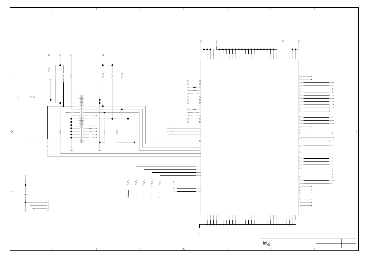
11-18-1999_11:32
PROCESSOR CONNECTOR
4
TMS_R
JP16
1
2
3
5,7
SEL133/100#
4
ITPPRDY#
EMI2
EMI3
EMI4
8,32
IGNNE# 8,32
FERR# 8,10,32
HINIT# 8,32
LINT1 8,32
LINT0 8,32
SMI# 8,32
SLP# 8,32
STPCLK# 8,32
A20M#
32
FLUSH#
32
BREQ#0 4
ITPPRDY# 4
ITPREQ#
6
HADS# 6
DBSY# 6
HIT# 6
HITM# 6
DRDY# 6
HLOCK# 6
DEFER# 6
HTRDY#
EMI5
5CPUHCLK
31 PWRGOOD
4,6 CPURST#
6
BPRI# 6
BNR#
8,32 PICD0
5PICCLK
EMI1
8,32 PICD1
5ITPCLK
32
TESTHI
28,31
VRM_PWRGD
TDI
TRST#
TMS
TCK
4
ITPREQ#
ITPRDY#_R
CPURST#_R
R149
240
4,6 CPURST#
TCK_R
ITP_PU_R
R163
47
47
R152
R138
240
R140
680
TDO
R19
240
1K
R157
1K
R167
R171
1K
0K
R101
0K
R104
0K
R103
0K
R93
0K
R100
R145
330
R139
330
150
R142
J15
9
87
65
4
30
3
29
2827
2625
2423
2221
20
2
19
1817
1615
1413
1211
10
1
J14
B9
B5
A3
A1
B53
B49
B45
B37
B33
B29
B25
B17
B105
B97
B93
B89
B85
B77
B73
B69
B65
B57
B13
B109
B121
B117
B113
B11
A104
B10
A15
A13
A11
A9
B7
B6
B3
B8
B101
B74
B20
B112
A113
A16
A12
A20
B23
B22
A19
B18
B106
B16
A17
B4
A8
A4
A109
B110
A115
A38
A34
A30
A26
A22
A18
A14
A118
A114
A110
A106
A102
A98
A94
A90
A86
A82
A10
A78
A74
A70
A66
A62
A58
A54
A50
A46
A42
A6
A2
B76
B2
A7
B41
B1
B81
B100
B61
B107
B28
A31
A29
B27
A28
B26
A27
A25
A105
A111
A75
B75
A76
A103
B24
A23
A21
B19
A101
A24
A77
B116
A117
B118
A5
B21
0.1UF
C80
31 DBRESET#
PCD PLATFORM DESIGN
REV:
DRAWN BY:
LAST REVISED:
PROJECT:
SHEET:
FOLSOM, CALIFORNIA 95630
1900 PRAIRIE CITY ROAD
87654321
A
B
C
D
12345678
D
C
B
A
1.01
TITLE: INTEL(R) 820 CHIPSET CUSTOMER REFERENCE BOARD
OF 36
R
VCC12
VCCVIDVTT1_5
VCC2_5
VCC5 VCC3_3
VTT1_5VCC2_5VCC3_3
A20M#
AERR#
AP0#
AP1#
BERR#
BINIT#
BNR#
BP2#
BP3#
BPM0#
BPM1#
BPRI#
BREQ0#
BREQ1#
BCLK
DBSY#
DEFER#
DEP#0
DEP#1
DEP#2
DEP#3
DEP#4
DEP#5
DEP#6
DEP#7
DRDY#
EMI_1
EMI_2
EMI_3
EMI_4
EMI_5
FERR#
FLUSH#
RES4
GND0
GND1
GND10
GND11
GND12
GND13
GND14
GND15
GND16
GND17
GND18
GND19
GND2
GND20
GND21
GND22
GND23
GND24
GND25
GND26
GND27
GND28
GND29
GND4
GND5
GND6
GND7
GND8
GND9
HADS#
HIT#
HITM#
IERR#
IGNNE#
INIT#
LINT0
LINT1
LOCK#
PICCLK
PICD0
PICD1
PRDY#
PREQ#
PWRGOOD
RES0
RES3
RES2
RES1
RESET#
SLOTOCC#
SLP#
SMI#
STPCLK#
TCK
TDI
TDO
TESTHI
THMTRP#
TMS
TRDY#
TRST#
VCC3_1
VCC3_2
VCC3_3
VCC5
VCCP1
VCCP10
VCCP11
VCCP12
VCCP13
VCCP14
VCCP15
VCCP16
VCCP17
VCCP18
VCCP19
VCCP2
VCCP3
VCCP4
VCCP5
VCCP6
VCCP7
VCCP8
VCCP9
VTT1
VTT2
VTT3
VTT4
BSEL0
BSEL1
SC242
ITP
CPU Fan Header
R163 and R152 should be placed within 1" of ITP connector.
Processor Connector
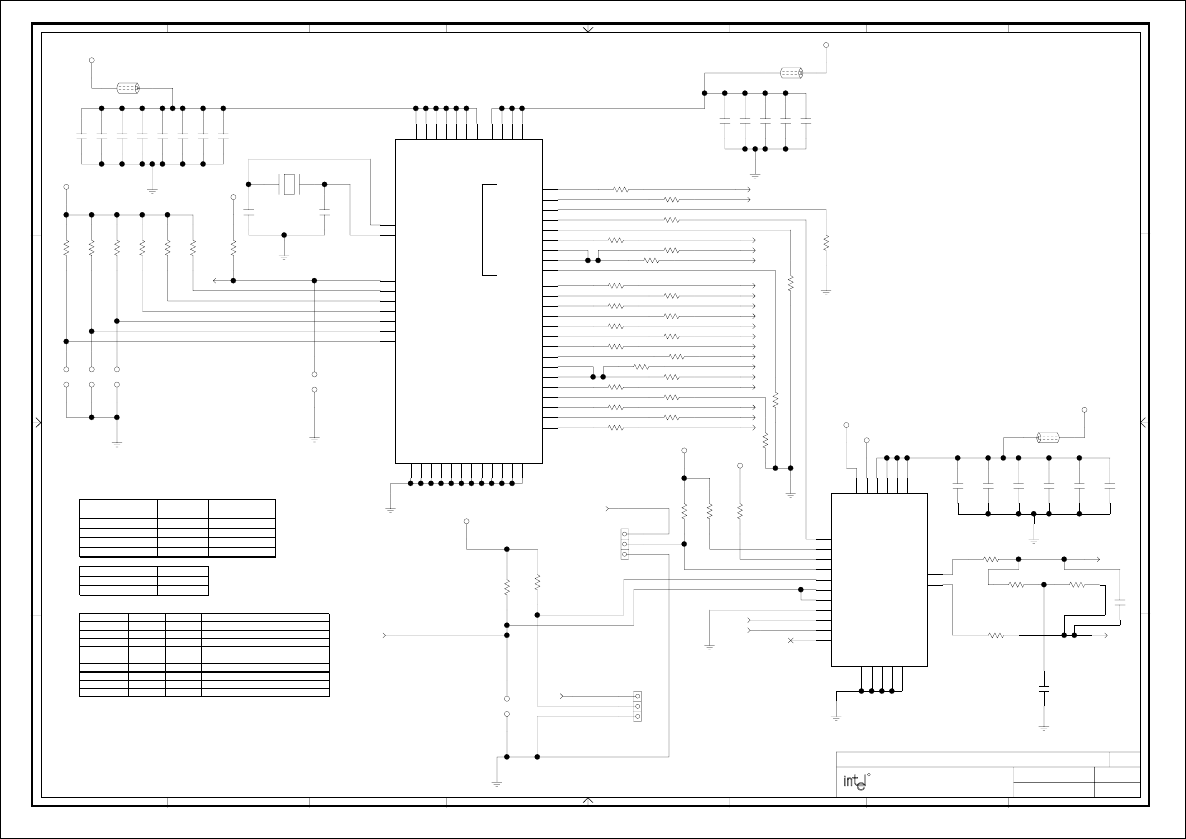
11-18-1999_11:33
CLOCK SYNTHESIZER
5
C364
82PF
4,7 SEL133/100#
JP19
4PF
C363
CK133_XIN
SIO_14MHZ_R
IHC_14MHZ_R
IHC_48MHZ_R
TEST_CLK66_R
ICH_CLK66_R
MCH_CLK66_R
SIO_PCLK7_R
FWHPCLK_R
PCLK5_R
PCLK4_R
PCLK3_R
PCLK2_R
PCLK1_R
ICHPCLK_R
CPUCLK3_R
CPUHCLK_R
ITPCLK_R
CPU_DIV2_2_R
APIC2_R
CK133_XOUT
VCC_3_3_CK133_FB
PCISTOP#
CPUSTOP#
CK133_PWRDWN#
SPREAD#
SEL0
VCC2_5_CK133_FB
APICCLK_R
PICCLK_R
33
R211
PCLK5 16
MULT1
R161
10K
10K
R206
10K
R203
JP15
JP11
7HCLKOUT
7RCLKOUT
R151
30
20
PCLK1
8
APICCLK
4
CPUHCLK 6
MCHCLK
14.318MHZ
Y3
21
22
R188
33
R165
33
R169
33
R186
33
R191
33
R183
21
PCLK3
21
PCLK4
10
FWHPCLK
9
ICH_14MHZ
R147 22
12
SIO_PCLK7
30
R166
AGPCLK_CONN 19
R195 33 7
MCH_CLK66
22
R221
R200
51-1%51-1%
R185
9
ICH_48MHZ
R217
10K
33
R194
10K
R202
9MULT0_GPIO
JP17
R196
10K
R192
10K
22 R184
22 R189
33 R201
33
R187
FBHS01L
L20 21
L21
FBHS01L
12
22
R155
4
PICCLK
R170
30
33
R220
9
ICH_CLK66
37TEST_CLK66
R150
22
8
ICHPCLK
20
PCLK2
DRCG_CLK
DRCG_CLKB# R205
39-1%
R182
39-1%
CLKTM_RD
0.1UF
C207
0.1UF
C215 C223
0.1UF
0.1UF
C186
0.1UF
C198
0.1UF
C206
0.1UF
C214
10PF
C185
10PF
C189
0.1UF
C199
0.1UF
C192
0.1UF
C190
0.1UF
C180
C204
0.1UF
0.1UF
C220
10UF
C209
0.1UF
C196
10UF
C171
10UF
C170
33
R210
12
SIO_14MHZ
R199
10K
R224
220
R197
10K
STOPB#
10K
R219
10K
R204
MULT0
DRCG_PWRDWN#
R156
22
CPU_DIV2_1_R R148
22
4
ITPCLK
33
R164
CPU_DIV2
9 DRCG_CTRL
JP13
3
2
1
9,12 MULT1_GPIO JP18
1
2
3
JP14
SEL1
VCC3_3_DRCG_FB FBHS01L
L22 12
11
CLKTM#
11
CLKTM
C208
0.1UF
U11
5
55
30
29
28
27
26
25
24
23
22
21
20
19
18
17
16
15
14
13
12
11
10
9
8
7
6
4
3
2
1
31
32
33
34
35
36
37
38
39
40
41
42
43
44
45
46
47
48
49
50
51
52
53
54
56
DRCG+
U12
21
17
2
12
11
24
23
22
20
18
16
15
14
10
7
6
9
8
5
4
3
1
13
0.1UF
C205
PCD PLATFORM DESIGN
REV:
DRAWN BY:
LAST REVISED:
PROJECT:
SHEET:
FOLSOM, CALIFORNIA 95630
1900 PRAIRIE CITY ROAD
87654321
A
B
C
D
12345678
D
C
B
A
1.01
TITLE: INTEL(R) 820 CHIPSET CUSTOMER REFERENCE BOARD
OF 36
R
VCC3_3
VCC3_3
XTAL
VCC3_3
VCC3_3
VCC2_5
VCC3_3
VCC2_5
VCC3_3
VCC1_8
VCC1_8
2_5V
CK133
VDD25V_1
APIC1
APIC0
VSS7
VDD25V_2
CPU_DIV2_1
CPU_DIV2_2
VSS8
VDD25V_3
CPUCLK3
CPUCLK2
VSS9
VDD25V_4
CPUCLK1
CPUCLK0
VSS10
VDD3V_6
VSS11
CPUSTOP#
PWRDWN#
SPREAD#
SEL1
SEL0
VDD3V_7
VSS1
REF0
REF1
VDD3V_1
XTAL_OUT
VSS2
PCICLK_F
PCICLK1
VDD3V_2
PCICLK2
PCICLK3
VSS3
PCICLK4
PCICLK5
VDD3V_3
PCICLK6
PCICLK7
VSS4
VSS5
3V66_0
3V66_1
VDD3V_4
VSS6
3V66_2
3V66_3
VDD3V_5
VSS12
48MHZ
APIC2
XTAL_IN
SEL133/100#
PCISTOP#
GND
VDDIR
VDDP
GNDP
GNDI
GNDC
VDDC
PCLKM
VDDIPD
MULT1
MULT0
VDDO1
CLKB#
CLK
VDDO2
S1
S0
STOPB#
PWRDN#
REFCLK
GNDO1
GNDO2
SYNCLKN
19 NC
Place C364 next to VDDP
JP19 is for debug only. CLKTM and CLKTM# RC network must use 5% or better tolerance components.
All jumpers may not be required, but are included for test purposes.
No stuff R106
for debug.
Provide at least one 0.1uF decoupling cap per power pin.
JP13 is for debug only.
VDDIR pin on DRCG should be decoupled at the component with a 0.1uF cap.
Keep stubs on unused outputs as short as possible.
Tie CPUCLK and MCHCLK outputs together.
Clock Synthesizer
No stuff R161, JP11.
No stuff C363
HOST
BUS /RAM BUS JP13 JP 18
100/300 2-3 OUT
100/400 OUT OUT
133/400 2-3 OUT
GPO CNTRL* 1-2 1-2
Sprd Spect JP14
Enabled* IN
Disabled OUT
SEL133/100# JP15 JP17 Function
0 IN IN All outputs Tri-State
0 IN OUT Reserved
0 OUT IN Active 100MHz, 48MHz PLL inactive
0 OUT OUT Active 100M Hz, 48MHz PLL active
1 IN IN Test Mode
1 IN OUT Reserved
1 OUT IN A ctive 133MHz,48M Hz PLL inactive
1 OUT OUT Active 133MHz,48MHz PLL active*
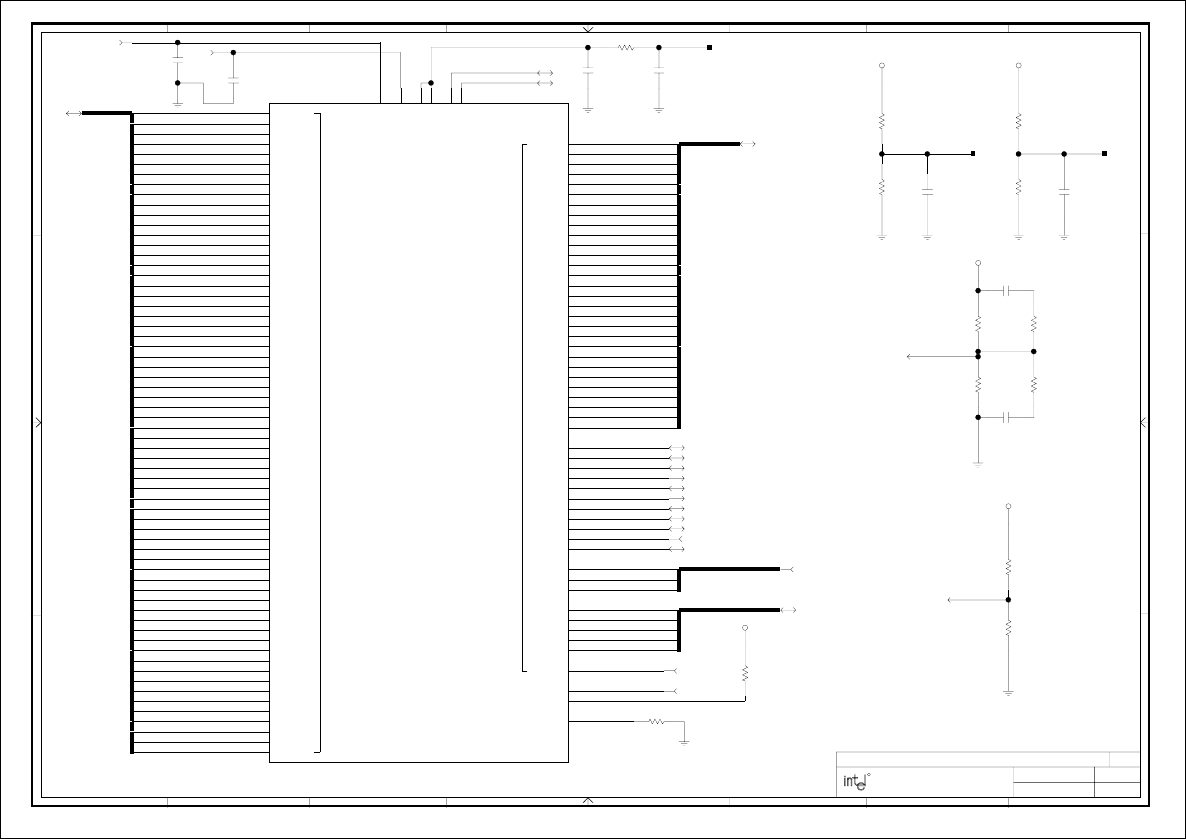
11-24-1999_11:15
MCH
6
HD#[63:0]
3HD#0
HD#1
HD#2
HD#3
HD#4
HD#5
HD#6
HD#7
HD#8
HD#9
HD#10
HD#11
HD#12
HD#13
HD#14
HD#15
HD#16
HD#17
HD#18
HD#19
HD#20
HD#21
HD#22
HD#23
HD#24
HD#25
HD#26
HD#27
HD#28
HD#29
HD#30
HD#31
HD#32
HD#33
HD#34
HD#35
HD#36
HD#37
HD#38
HD#39
HD#40
HD#41
HD#42
HD#43
HD#44
HD#45
HD#46
HD#47
HD#48
HD#49
HD#50
HD#51
HD#52
HD#53
HD#54
HD#55
HD#56
HD#57
HD#58
HD#59
HD#60
HD#61
HD#63
HD#62
GRCOMP
MCH_HLCOMP
PCIRST# 8,10,11,12,16,19,20,21,22
MCHCLK 5
3
HREQ#[4:0]
HREQ#4
HREQ#3
HREQ#2
HREQ#1
HREQ#0
RS#[2:0]
3
RS#2
RS#1
RS#0
HTRDY# 4
HLOCK# 4
HITM# 4
HIT# 4
DRDY# 4
DEFER# 4
DBSY# 4
BPRI# 4
BNR# 4
HADS# 4
CPURST# 4
3
HA#[31:0]
HA#3
HA#4
HA#5
HA#6
HA#7
HA#30
HA#31
HA#29
HA#28
HA#27
HA#26
HA#25
HA#24
HA#23
HA#22
HA#21
HA#20
HA#19
HA#18
HA#17
HA#16
HA#15
HA#14
HA#13
HA#12
HA#11
HA#10
HA#9
HA#8
8,37 HUBREF
19 CONN_AGPREF RAMREF_R
6GTLREF2
6GTLREF1
MCH_AGPREF_CV
R143
75-1%
RAMREF 6,11
19
MCH_AGPREF
R190
162-1%
RAMREF
6,11
100-1%
R168
40.2-1%
R180
MCH_AGPREF_CG
40.2-1%
R129
R131
75-1%150-1%
R130
R144
150-1%
0.1UF
C155
0.1UF
C191
0.1UF
C203
C158
0.001UF
C182
470PF
562-1%
R181
0.001UF
C183
C187
470PF
U10
V2
Y1
W2
C3
V12
E11
E10
U14
E20
T15
A18
F20
G2
E3
E4
G4
H1
E2
C1
E5
F4
F3
E1
D3
F1
F2
D1
G1
F5
D2
P4
M5
N4
P3
P2
N1
P1
M4
N5
M1
M2
M3
N2
L2
K4
L4
K3
K5
J2
K1
J5
L1
J4
H2
H5
K2
G5
H4
H3
J1
W13
V14
Y14
U12
U11
W14
Y12
Y13
U13
T11
W12
V10
U10
T12
T10
Y11
T9
W11
Y9
U9
V8
Y10
W10
U8
W9
T7
W8
T8
Y7
Y8
U7
W7
T6
W6
V6
U6
W5
Y6
T5
V5
T4
Y5
Y4
T3
U4
V4
W3
W4
U2
U3
Y3
T2
U1
W1
Y2
V1
R5
T1
P5
R4
R1
R2
GTLREF2 GTLREF1
1K-1%
R154
1K-1%
R159
R160
80.6-1%
R153
80.6-1%
0.01UF
C194
PCD PLATFORM DESIGN
REV:
DRAWN BY:
LAST REVISED:
PROJECT:
SHEET:
FOLSOM, CALIFORNIA 95630
1900 PRAIRIE CITY ROAD
87654321
A
B
C
D
12345678
D
C
B
A
1.01
TITLE: INTEL(R) 820 CHIPSET CUSTOMER REFERENCE BOARD
OF 36
R
VDDQ
VCC1_8
VTT1_5 VTT1_5
VCC1_8
VDDQ;F15,R15,J17,L17,N17,T17
MCH_096
GND;D9,J9,K9,L9,M9,V9,B10,J10,K10,L10,M10,C11,J11,K11,L11
GND;P19,T19,D20
GND;B15,D15,B16,D16,E16,F16,A17,E18,V18,A19,H19,K19,M19
HD#0
HD#1
HD#2
HD#3
HD#4
HD#5
HD#6
HD#7
HD#8
HD#9
HD#10
HD#11
HD#13
HD#15
HD#16
HD#17
HD#18
HD#19
HD#20
HD#21
HD#22
HD#23
HD#24
HD#25
HD#26
HD#27
HD#28
HD#29
HD#30
HD#31
HD#32
HD#33
HD#34
HD#35
HD#36
HD#37
HD#38
HD#39
HD#40
HD#41
HD#42
HD#43
HD#44
HD#45
HD#46
HD#47
HD#48
HD#49
HD#50
HD#51
HD#52
HD#53
HD#54
HD#55
HD#56
HD#57
HD#58
HD#59
HD#60
HD#61
HD#62
HD#63
HA#3
HA#4
HA#5
HA#6
HA#7
HA#8
HA#9
HA#10
HA#11
HA#12
HA#13
HA#14
HA#15
HA#16
HA#17
HA#18
HA#19
HA#20
HA#21
HA#22
HA#23
HA#24
HA#25
HA#26
HA#27
HA#28
HA#29
HA#30
HA#31
CPURST#
ADS#
BNR#
BPRI#
DBSY#
DEFER#
DRDY#
HIT#
HITM#
HLOCK#
HTRDY#
RS#0
RS#1
RS#2
HREQ#0
HREQ#1
HREQ#2
HREQ#3
HREQ#4
RSTIN#
HUBREF
AGPREF
RAMREFB
RAMREFA
GTLREFB
GTLREFA
HD#12
HD#14
HCLKIN
TEST/GRCOMP
HLCOMP
VCC1_8;D4,E6,F6,G6,E7,R6,R7,E8,E9,D10,D11,E12
VCC1_8;E13,E14,F14,T14,E15,P15,B17,C17,C19
GND;A1,A3,G3,J3,L3,N3,R3,V3,B4,D5,L5,U5,B6,D6,D7,V7,B8,D8
GND;M11,V11,C12,D12,J12,K12,L12,M12,B13,D13,V13,T13,D14
HOST HOST
Place R129 and R180 less than 0.5" from MCH using 10 mil trace.
Place MCH_AGPREF circuit near the MCH.
MCH
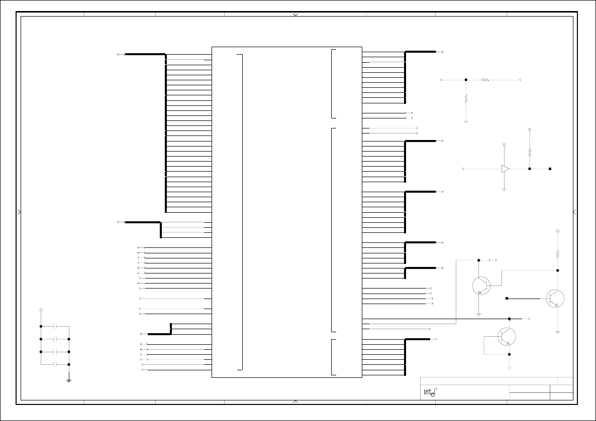
11-18-1999_11:34
MCH
7
C360
0.1UF
0.1UF
C359 C361
0.1UF
0.1UF
C362
4.7K
R248
PWROK9,16,29,31
U14
14
7
13 12
11LCMD
LSCK
11
SCK_CTRL
HL10
7,8,37
GAD1
GAD2
GAD3
GAD4
GAD5
GAD6
GAD7
GAD8
GAD9
GAD10
GAD11
GAD12
GAD13
GAD14
GAD15
GAD16
GAD17
GAD18
GAD19
GAD20
GAD21
GAD22
GAD23
GAD24
GAD25
GAD26
GAD27
GAD28
GAD29
GAD30
GAD31
19
GAD[31:0] GAD0
HL2
HL1
HL[10:0]
8
HL0
HL10
HL9
HL8
HL7
HL6
HL5
HL4
HL3
HL_STB 8,37
HL_STB# 8,37
11
LCLKFM# 11
LCLKFM 11
LCLKTM# 11
LCLKTM
LDQB0 11
LDQB[8:0]
LDQB1
LDQB2
LDQB3
LDQB4
LDQB5
LDQB6
LDQB7
LDQB8
LCOL0 11
LCOL[4:0]
LCOL1
LCOL2
LCOL3
LCOL4
11
LROW[2:0]
LROW0
LROW1
LROW2
LDQA6
LDQA7
LDQA8
LDQA4
LDQA3
LDQA2
LDQA1
LDQA0 11
LDQA[8:0]
LDQA5
GC/BE#2
GC/BE#1
GC/BE#0
GC/BE#[3:0]
19
GC/BE#3
19,32 GTRDY#
19,32 GIRDY#
19,32 GDEVSEL#
19,32 GFRAME#
GPAR
19,32
19,32 GSTOP#
SBSTB#
19,32
ADSTB1
19,32
ADSTB0
19,32
WBF#
19,32
19,32 PIPE#
19,32 GREQ#
19,32 GGNT#
ST2
ST0
ST1
ST[2:0]
19
5MCH_CLK66
19,32 RBF#
ADSTB#0
19,32
ADSTB#1
19,32 SBSTB
19,32
HCLKOUT 5
RCLKOUT 5
19
SBA[7:0]
SBA1
SBA3
SBA4
SBA5
SBA6
SBA7
SBA2
SBA0
LSIO 11
4,5
SEL133/100#
R209
8.2K
Q10
MMBT3904LT1
B
C
E
4.7K
R346
MMBT3904LT1
Q14
E
C
B
MMBT3904LT1
Q9
B
C
E
8.2K
R227
7
PWROK_CTRL
PWROK_CTRL7
U10
Y19
Y20
W17
Y18
W18
A16
A9
B9
C9
F19
C4
A4
B5
A5
C5
A6
C6
B7
C7
C16
A15
C15
B14
C14
A14
C13
A13
A2
B1
C20
D19
D18
C18
D17
A20
B18
B19
B20
E19
E17
F18
A7
C8
A8
A10
C10
B11
A11
A12
B12
B3
B2
C2
W20
V17
V20
W19
V19
U16
R19
R18
H20
J19
Y17
Y15
W15
V15
V16
W16
Y16
U15
K16
M18
M20
N20
N19
L16
R16
N18
L20
H16
U19
U20
T18
U18
T16
U17
R17
T20
R20
P16
P20
N16
P17
M16
P18
M17
L18
K20
L19
J18
K18
K17
J16
J20
H18
H17
G20
G16
G19
G17
G18
F17
PCD PLATFORM DESIGN
REV:
DRAWN BY:
LAST REVISED:
PROJECT:
SHEET:
FOLSOM, CALIFORNIA 95630
1900 PRAIRIE CITY ROAD
87654321
A
B
C
D
12345678
D
C
B
A
1.01
TITLE: INTEL(R) 820 CHIPSET CUSTOMER REFERENCE BOARD
OF 36
R
VCC1_8
VCC3_3SBY
SN74LVC07A GND
VCC
VCC5SBY
1
3
2
13
2
13
2
VCC3_3SBY
MCH_096
HUB
AGP
MEMORY
AGP
G_AD0
G_AD1
G_AD2
G_AD3
G_AD4
G_AD5
G_AD6
G_AD7
G_AD8
G_AD9
G_AD10
G_AD11
G_AD12
G_AD13
G_AD14
G_AD15
G_AD16
G_AD17
G_AD18
G_AD19
G_AD20
G_AD21
G_AD22
G_AD23
G_AD24
G_AD25
G_AD26
G_AD27
G_AD28
G_AD29
G_AD30
G_AD31
G_C/BE#0
G_C/BE#1
G_C/BE#2
G_C/BE#3
G_FRAME#
G_DEVSEL#
G_IRDY#
G_TRDY#
G_STOP#
G_PAR
G_REQ#
G_GNT#
PIPE#
RBF#
WBF#
ST0
ST1
ST2
AD_STB0
AD_STB#0
AD_STB1
AD_STB#1
SBA7
SBA6
SBA5
SBA4
SBA1
SBA0
SIO
SCK
CMD
CFM#
CFM
CTM#
CTM
RQ7
RQ6
RQ2
RQ1
RQ0
HL1
HL2
HL3
HL4
HL5
HL6
HL7
HL8
HL9
HL10
HL_STB
HL_STB#
RCLKOUT
HCLKOUT
DQA0
DQA1
DQA2
DQA3
DQA4
DQA5
DQA6
DQA7
DQB0
DQB1
DQB2
DQB3
DQB4
DQB5
DQB6
DQB7
DQB8
HL0
RQ3
RQ4
RQ5
DQA8
CLK66
SBA2
SBA3
SB_STB
SB_STB#
LSCK and LCMD must neck down to 5 mils for 175 mils at Q10 and Q9 attach points.
Place Q10 and Q9 as close as possible to MCH.
MCH
No stuff. For test only.
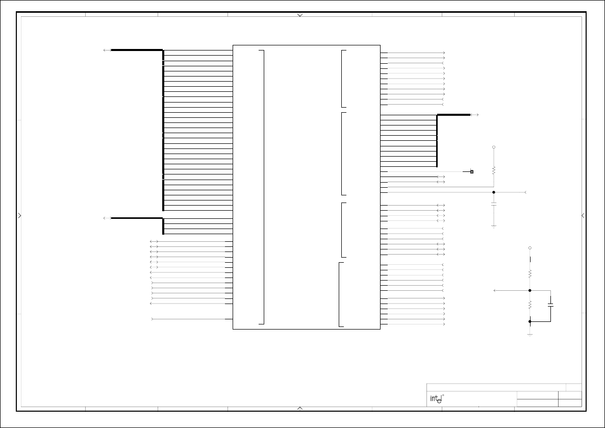
11-24-1999_11:14 8
ICH
6,8,37 HUBREF
PGNT#5 21,32
PGNT#4 32
PGNT#3 16,32
21,32
PGNT#2
PGNT#1 20,32
PGNT#0 20,32
PREQ#5 21,32
PREQ#4 32
PREQ#3 16,32
PREQ#2 21,32
PREQ#1 20,32
20,32
PREQ#0
12,21,32
SERIRQ 4,32
PICD1
PICD0 4,32
5
APICCLK
IRQ15 22,32
IRQ14 22,32
20,21,32
PIRQ#D
PIRQ#C 20,21,32
19,20,21,32
PIRQ#B
PIRQ#A 16,19,20,21,32
6,8,37HUBREF
7,37
HL_STB#
7
HL[10:0]
HL10
HL9
HL8
HL7
HL6
HL5
HL4
HL3
HL2
HL1
HL0
AD[31:0]
16,20,21 AD0
AD1
AD2
AD3
AD4
AD5
AD6
AD7
AD8
AD9
AD10
AD11
AD12
AD13
AD14
AD15
AD16
AD17
AD18
AD19
AD20
AD21
AD22
AD23
AD24
AD25
AD26
AD27
AD28
AD29
AD30
AD31
16,20,21
C_BE#[3:0] C_BE#0
C_BE#1
C_BE#2
C_BE#3
DEVSEL#
16,20,21,32 FRAME#
16,20,21,32 IRDY#
16,20,21,32 TRDY#
16,20,21,32 STOP#
16,20,21,32 PAR
16,20,21 PCIRST#
6,10,11,12,16,19,20,21,22 PLOCK#
20,21,32 SERR#
16,20,21,32 PERR#
16,20,21,32
16,19,20,21 PCI_PME#
ICHPCLK
5
12,32
A20GATE 12,32
KBRST#
STPCLK# 4,32
4,32
SMI# 4,32
LINT1 4,32
LINT0
HINIT# 4,10,32
IGNNE# 4,32
4,32
FERR# 4,32
SLP#
A20M# 4,32
R226
301-1%
R225
301-1%
40.2-1%
R239
21,32 REQ#A
21,32 GNT#A
ICH_HLCOMP
HL11_TP
U13
M17
H17
G17
J17
H15
L17
K17
K16
G16
F17
D17
K1
E9
E2
E1
F5
F4
F3
F2
G4
G2
C13
A13
N6
D10
C14
R5
P5
J13
R4
C17
E16
F14
A15
B15
A17
B10
B7
E7
D8
C7
A12
C12
B13
D12
B11
B12
A14
F16
J14
B16
E14
B17
B9
A9
C4
D5
B3
D9
D6
A3
B2
D2
B4
C5
A8
B6
D7
A6
B5
C2
B8
A7
A4
C6
D4
C3
E4
D3
D1
C1
J15
A1
N14
A2
E15
E12
C16
B1
F13
E17
J5
A11
C9
F15
P11
A10
C10
P4
HL_STB 7,37
TP1
0.1UF
C218
0.01UF
C237
PCD PLATFORM DESIGN
REV:
DRAWN BY:
LAST REVISED:
PROJECT:
SHEET:
FOLSOM, CALIFORNIA 95630
1900 PRAIRIE CITY ROAD
87654321
A
B
C
D
12345678
D
C
B
A
1.01
TITLE: INTEL(R) 820 CHIPSET CUSTOMER REFERENCE BOARD
OF 36
R
VCC1_8
CPU
HUB
IRQ
ICH_A
PCI
PCI
GND;R2,G3,H8,J8,K8,H9,J9,K9,H10,J10,K10,G14,K15
VCC3_3;E3,A5,E5,G5,N5,E6,P6,T7,C8,U10
VCC3_3;C11,E13,N13,R13,M14,D16,T16
VCC1_8;G13,H14,K14,G15,L15,H16,J16
ICH_096
GPIO1/REQ#B/REQ#5
PIRQD#
PIRQB#
IRQ14
FERR#
AD29
GNT#4
PCIRST#
HL1
A20M#
AD13’
APICCLK
CPUSLP#
INIT#
IRDY#
IRQ15
SERR#
HL4
AD12
AD8
AD9
AD10
AD15
AD14
AD19
AD16
AD26
AD25
AD11
AD20
AD22
AD24
AD23
AD27
AD18
AD17
CBE0#
CBE#1
CBE#2
CBE#3
DEVSEL#
FRAME#
STOP#
TRDY#
PAR
PLOCK#
IGNNE#
INTR
NMI
HL10
HL11
REQ#0
REQ#2
REQ#4
REQ#3
REQ#1
GNT#3
GNT#2
AD31
AD30
AD21
AD28
PIRQC#
STPCLK#
A20GATE
RCIN#
SMI#
APICD0
APICD1
SERIRQ
HUBREF
GPIO16/GNT#A
GPIO17/GNT#B/GNT#5
PCICLK
PIRQA#
GPIO0/REQ#A GNT#0
GNT#1
AD0
AD1
AD2
AD3
AD4
AD5
AD6
AD7
PERR#/GPIO7
PME#
HL0
HL2
HL3
HL5
HL6
HL7
HL8
HL9
HL_STB
HL_STB#
HLCOMP
VCC1_8
HUBREF voltage = 0.9V +/- 2%
Place HUBREF circuit between MCH and ICH
Place R239 less than 0.5" from the ICH using a 10 mil trace.
Place C237 close to ICH.
ICH
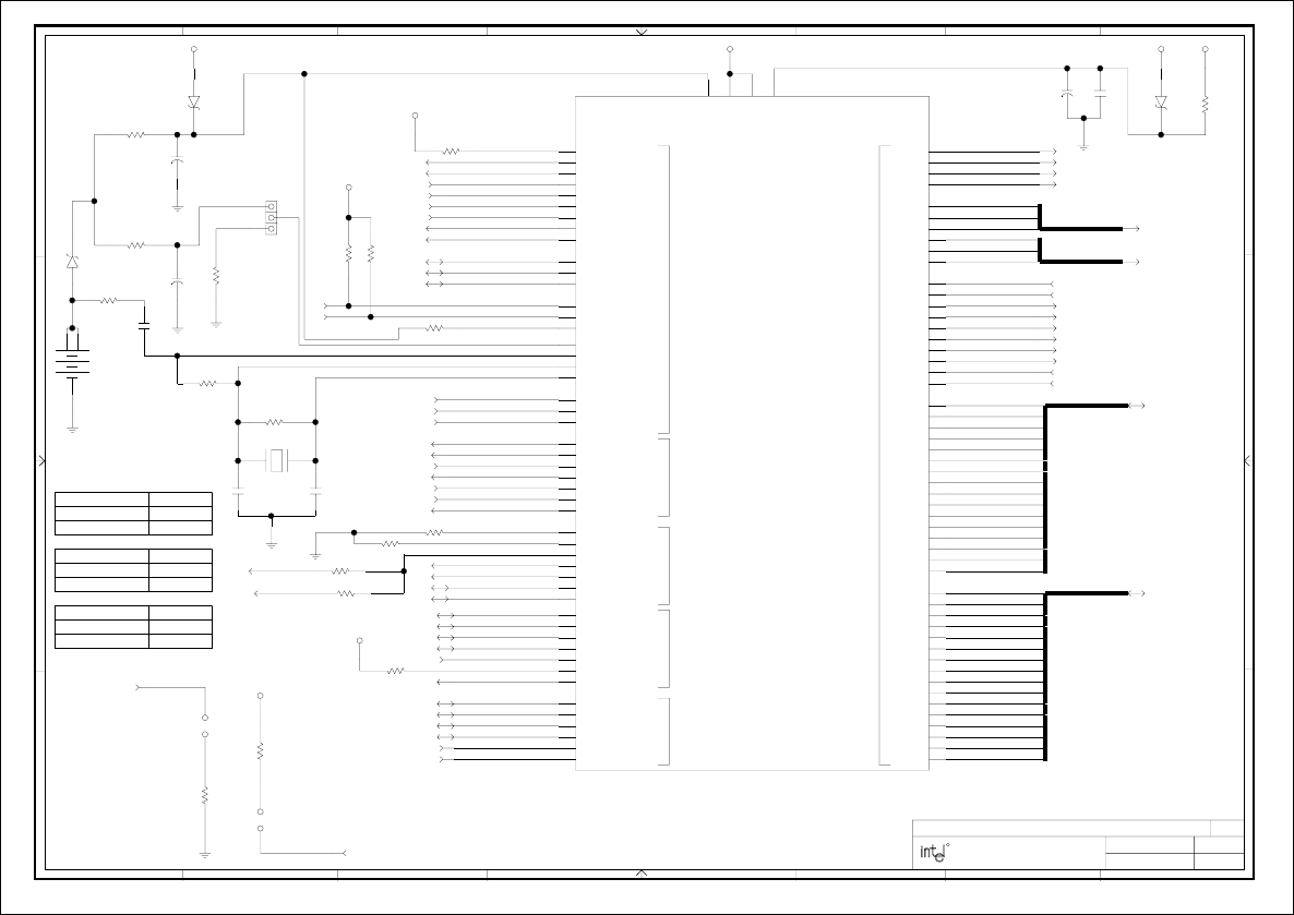
12-2-1999_16:22 9
ICH
GPIO21
DRCG_CTRL5
GPIO12
GPIO13
8.2K
R254
LPC_SMI#
12 LPC_PME#
12
RTCX1
VBAT_RTC
18 GPIO26_FPLED
AC_SDOUT_STRAP
JP5
1K
R250
8.2K
R232
13,15 AC_BITCLK
7,16,29,31 PWROK
SMBDATA_CORE3,11,32
SMBCLK_CORE3,11,32
15 AC_RST#
13,15 AC_SYNC
13,15 AC_SDATAIN0
15 AC_SDATAIN1
9,18 SPKR
10,12 LAD0/FWH0
LAD1/FWH1
10,12
10,12 LAD2/FWH2
10,12 LAD3/FWH3
LFRAME#/FWH4
10,12
USBP1P
23 USBP1N
23 USBP0P
23 USBP0N
23
22
SIORDY 22
PIORDY
SDIOW# 22
PDIOW# 22
SDIOR# 22
PDIOR# 22
SDDACK# 22
PDDACK# 22
SDREQ 22
PDREQ 22
SDA2
SDA0
22
SDA[2:0]
SDA1
PDA1
PDA0
PDA2 22
PDA[2:0]
22
SDCS#3 22
PDCS#3
SDCS#1 22
PDCS#1 22
OC#1
23 OC#0
23
1K
R230
32.768KHZ
Y4
21
29,31 SLP_S3#
PDD14
PDD13
PDD12
PDD11
PDD10
PDD9
PDD8
PDD7
PDD6
PDD5
PDD4
PDD3
PDD2
PDD1
PDD0 PDD[15:0]
22
PDD15
SDD12
SDD13
SDD14
SDD15
SDD11
SDD10
SDD9
SDD8
SDD7
SDD6
SDD5
SDD4
SDD3
SDD2
SDD1
SDD[15:0]
22
SDD0
R233
1K
R245
1K
ICH_CLK66
5ICH_14MHZ
5ICH_48MHZ
5
R341
2.7K
MULT0_GPIO
5
32 SMB_ALERT
PWRBTN#
18
25 ICH_RI#
9,18 SPKR
10M
R249
12 LDRQ#0
30 SLP_S5#
INTRUDER#
8.2K
R231 3THRM#
RTC_CLR
GPIO8
SPKR_STRAP
VBAT_CR
VCC5_REF
8.2K
R241
JP26
VBAT_RC
2.7K
R90
R238
8.2K
RSMRST#
17,31
5,12 MULT1_GPIO
12PF
C251
0.1UF
C233
C250
12PF
1UF
C246
1
2
1UF
C234
2
1
BAT17
CR5
C
A
BAT17
CR4
A
C
BAT17
CR3
C
A
U13
L5
J3
L1
N1
C15
J4
M1
L4
P16
R17
R15
U17
T15
P14
T14
U14
T13
P13
R14
U15
U16
T17
R16
P15
H1
H3
P10
T10
P9
T9
P8
T8
N7
P7
U8
U7
R7
R8
U9
R9
N9
R10
N17
N11
N15
T11
N16
R11
M13
U12
P17
U11
L13
M15
M16
T12
R12
L16
U13
L14
N12
U4
T4
T5
U5
R6
D15
H4
H2
E11
D11
K4
F1
M2
G1
A16
N4
L2
M5
K2
J1
P3
U6
D13
B14
U1
T2
U2
T3
U3
N3
T6
P1
P2
N2
R1
M3
M4
J2
P12
L3
T1
D14
K3
R3
GPIO23_FPLED
18 ALERTCLK_SBY
16,32 ALERTDATA_SBY
16,32
JP20
3
2
1
RTC_RST_JP
BAT1
12
3
VBIAS
RTCX2
R247
10M
9,13,15 AC_SDATAOUT
AC_SDATAOUT 9,13,15
RTCRST#
VCC_RTC_JP
8.2K
R317
R212
8.2K
8.2K
R215
R98
0K
21 PCI_TEST
0K
R162
C247
2.2UF
2
1
0.047UF
C249
PCD PLATFORM DESIGN
REV:
DRAWN BY:
LAST REVISED:
PROJECT:
SHEET:
FOLSOM, CALIFORNIA 95630
1900 PRAIRIE CITY ROAD
87654321
A
B
C
D
12345678
D
C
B
A
1.01
TITLE: INTEL(R) 820 CHIPSET CUSTOMER REFERENCE BOARD
OF 36
R
VCC3_3
VCC3_3 VCC5VCC3_3SBY
XTAL
VCC3_3
VCC3_3SBY
VCC3_3SBY
VCC3_3
+
+
-
+
-
+
-
+
SYSTEM
LPC
AC97
USB
GPIO
IDE
ICH_B
ICH_096
AC_BIT_CLK
GPIO24/SLP_S3#
THRM#
AC_RST#
RI#
PDA2
SMBCLK
OC1#
OC0#
USBP1+
USBP0-
USBP1-
USBP0+
LDRQ0#
GPIO8/LDRQ1#
SPKR
AC_SYNC
CLK48
AC_SDOUT
ACSDIN0
GPIO21
GPIO22
CLK14
GPIO9/AC_SDIN1
SMBDATA
SLP_S5#
GPIO27/ALERT_CLK
GPIO13
GPIO12
CLK66
VCCRTC
PWRBTN#
RSMRESET#
SUSCLK/GPIO26
GPIO5
GPIO6
VBIAS
RTCX2
GPIO23
LAD0/FWH0
LAD1/FWH1
LAD2/FWH2
LAD3/FWH3
LFRAME#/FWH4
PDCS1#
SDCS1#
PDCS3#
SDCS3#
PDA0
PDA1
SDA0
SDA1
SDA2
PDDREQ
SDDREQ
PDDACK#
SDDACK#
PDIOR#
SDIOR#
PDIOW#
SDIOW#
PIORDY
SIORDY
PDD0
PDD1
PDD2
PDD3
PDD4
PDD6
PDD7
PDD5
PDD8
PDD9
PDD10
PDD11
PDD12
PDD13
PDD14
PDD15
RTCX1
RTCRST#
SDD0
SDD1
SDD2
SDD3
SDD4
SDD5
SDD6
SDD7
SDD8
SDD9
SDD10
SDD11
SDD12
SDD13
SDD14
SDD15
GPIO25/SUSSTAT#
GPIO11/SMBALERT#
GPIO10/INTRUDER#
VCC5REF
VCCSUS
VCCSUS1
PWROK
GPIO28/ALERT_DATA
+
+
ICH
Use CR2032 battery.
No stuff R98.
Strap JP26
No WD Reboot IN
Reboot on WD* OUT
Strap JP5
Safe Mode IN
ICH s trap* OUT
CMOS JP20
Norm al* 1-2
Clear 2-3
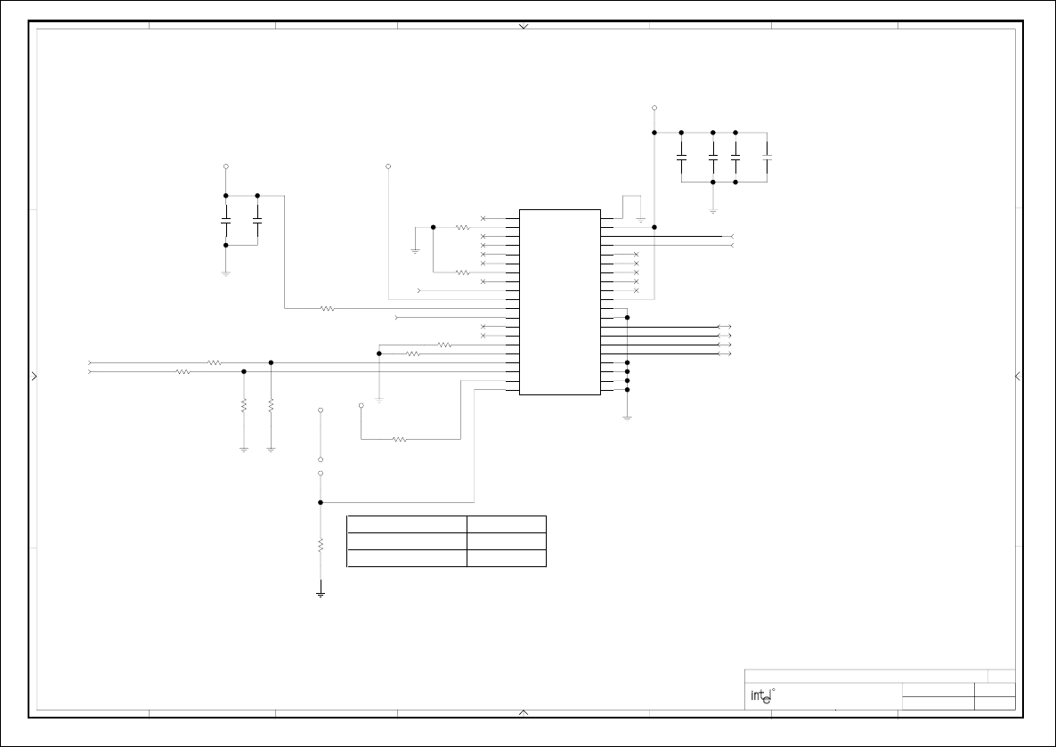
11-18-1999_10:44
FWH
10
8.2K
R303
FGPI0
FGPI1
R307
15K
R304
15K
TBLK_LCK
9,12
LFRAME#/FWH4
9,12
LAD3/FWH3
LAD2/FWH2 9,12
LAD1/FWH1 9,12
LAD0/FWH0 9,12
6,8,11,12,16,19,20,21,22 PCIRST#
5FWHPCLK
WPROT
4,8,32
HINIT#
R299
0K
JP21
4.7K
R308
8.2K
R298
R296
8.2K
VPP_R
FGPI3
FGPI2
FGPI4
FWH_IC
U16
18
17
16
15
7
40
39
38
37
36
35
34
33
32
31
30
29
28
27
26
25
24
23
22
2120
19
14
13
12
11
10
9
2
8
6
5
4
3
1
C300
0.1UF
C305
0.1UF
C301
0.1UF
C298
0.1UF
0.1UF
C297
0.1UF
C308
0K
R306
22 S66DETECT
22 P66DETECT 0K
R305
4.7K
R310
8.2K
R300
PCD PLATFORM DESIGN
REV:
DRAWN BY:
LAST REVISED:
PROJECT:
SHEET:
FOLSOM, CALIFORNIA 95630
1900 PRAIRIE CITY ROAD
87654321
A
B
C
D
12345678
D
C
B
A
1.01
TITLE: INTEL(R) 820 CHIPSET CUSTOMER REFERENCE BOARD
OF 36
R
VCC3_3
VCC3_3 VCC3_3
VCC3_3
VCC3_3
NC1
NC3
NC4
NC5
NC6
NC8
IC
CLK
VCC10
VPP
RST#
NC13
NC14
WP#
TBL# ID3
ID2
ID1
ID0
FWH0
FWH1
FWH2
FWH3
GND29
GND30
VCC31
RFU32
RFU33
RFU34
RFU35
RFU36
INIT#
FWH4
VCCA
GNDA
FGPI4
FGPI3
FGPI2
FGPI1
FGPI0
FWH
Top Block Lock
to VCC3_3 for onboard programming.
Do not tie Vpp to 12V. Vpp should be tied
For host side detection, stuff R304,R305,R306,R307.
For drive side detection, stuff R304,R307. No stuff R305,R306.
FWH
FWH JP21
OUT Locked
IN Unloc k ed*
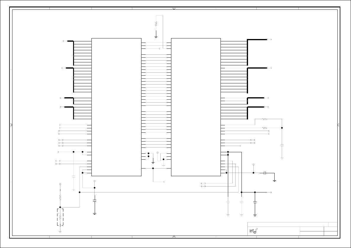
11-24-1999_13:14 11
RIMM SOCKETS
6,8,10,12,16,19,20,21,22
PCIRST#
CLKTM# 5
TERM_DQB0 33
TERM_DQB[8:0]
TERM_DQB8
TERM_DQB7
TERM_DQB6
TERM_DQB5
TERM_DQB4
TERM_DQB3
TERM_DQB2
TERM_DQB1
33
TERM_DQA[8:0]
TERM_DQA0
TERM_DQA8
TERM_DQA7
TERM_DQA6
TERM_DQA5
TERM_DQA4
TERM_DQA3
TERM_DQA2
TERM_DQA1
33TERM_SCK
33TERM_CMD
LDQA[8:0]
7LDQA0
LDQA1
LDQA2
LDQA3
LDQA4
LDQA5
LDQA6
LDQA7
LDQA8
LCOL[4:0]
7LCOL4
LCOL3
LCOL2
LCOL1
LCOL0
LDQB[8:0]
7
LDQB8
LDQB7
LDQB6
LDQB5
LDQB4
LDQB3
LDQB2
LDQB1
LDQB0
LROW[2:0]
7
LROW0
LROW1
LROW2
7LCLKTM
7LCLKFM#
7LCLKFM
7LCLKTM#
7LCMD
7LSCK
7LSIO
RAMREF
6,11
11MR1OUT
28-1%
R286
C228
0.1UF
0.1UF
C256
28-1%
R287
0.1UF
C291
3,9,11,32
SMBCLK_CORE
MR1OUT11
CLKTM 5
CLKFM#
CLKFM
RCMD_A
RSCK_A
RDQA0_A
RDQA1_A
RDQA2_A
RDQA3_A
RDQA4_A
RDQA5_A
RDQA6_A
RDQA7_A
RDQA8_A
RDQB0_A
RDQB1_A
RDQB2_A
RDQB3_A
RDQB4_A
RDQB5_A
RDQB6_A
RDQB7_A
RDQB8_A
RROW0_A
RROW1_A
RROW2_A
RCOL0_A
RCOL1_A
RCOL2_A
RCOL3_A
RCOL4_A
RCFM_A
RCFMN_A
RCTM_A
RCTMN_A
CTERM_RIMM
3,9,11,32
SMBDATA_CORE
R228
4.7K
0.1UF
C243
4.7K
R229
8.2K
R500
TERM_ROW1
TERM_ROW2
TERM_ROW0
33
TERM_ROW[2:0]
TERM_COL[4:0] 33
TERM_COL1
TERM_COL2
TERM_COL3
TERM_COL4
TERM_COL0
6,11RAMREF
3,9,11,32 SMBCLK_CORE
3,9,11,32 SMBDATA_CORE
MR2OUT
SWP
J16
A81
B81
A12
B12
B18
A18
A36
B36
A51
A59
B56
B16
B8
A10
A8
B59
B38
A57
B57
B55
A55
A79
A20
A22
B24
B6
A6
B4
A4
B2
A2
A26
B26
A28
B28
A30
B30
A32
B32
B20
B22
A24
B10
A14
B34
A34
B51
A53
A83
B85
A85
B87
A87
B89
A89
B91
A91
B69
A67
B67
A65
B65
A63
B63
A61
B61
B75
A75
B77
A69
B71
A71
B73
A73
B83
B53
A56
J18
A81
B81
A12
B12
B18
A18
A36
B36
A51
A59
B56
B16
B8
A10
A8
B59
B38 A57
B57
B55
A55
A79
A20
A22
B24
B6
A6
B4
A4
B2
A2
A26
B26
A28
B28
A30
B30
A32
B32
B20
B22
A24
B10
A14
B34
A34
B51
A53
A83
B85
A85
B87
A87
B89
A89
B91
A91
B69
A67
B67
A65
B65
A63
B63
A61
B61
B75
A75
B77
A69
B71
A71
B73
A73
B83
B53
A56
C236
0.1UF
0.1UF
C165
C169
0.1UF
PCD PLATFORM DESIGN
REV:
DRAWN BY:
LAST REVISED:
PROJECT:
SHEET:
FOLSOM, CALIFORNIA 95630
1900 PRAIRIE CITY ROAD
87654321
A
B
C
D
12345678
D
C
B
A
1.01
TITLE: INTEL(R) 820 CHIPSET CUSTOMER REFERENCE BOARD
OF 36
R
VCC3_3
VCC3_3
VCC3_3
VCC3_3
GND;B52,B60,B62,B64,B66,B68,B70,B72,B74,B76,B78,B80,B82,B84,B86,B88,B90,B92
GND;B1,B3,B5,B7,B9,B11,B13,B15,B17,B29,B21,B23,B25,B27,B19,B31,B33,B39
GND;A52,A60,A62,A64,A66,A68,A70,A72,A74,A76,A78,A80,A82,A84,A86,A88,A90,A92
GND;A1,A3,A5,A7,A9,A11,A13,A15,A17,A29,A21,A23,A25,A27,A19,A31,A33,A39
RIMM
VCC2_5SBY;A41,A42,A54,A58,B41,B42,B54,B58
VCMOS1_8SBY;A35,A37,B35,B37
NC;A16,A77,B14,B79
SVDDA
SA0
RCFM
RCOL4
RCOL3
RCOL2
RCOL1
RCOL0
RROW2
RROW1
RROW0
RDQB8
RDQB7
RDQB6
RDQB5
RDQB4
RDQB3
RDQB2
RDQB1
RDQB0
RDQA8
RDQA7
RDQA6
RDQA5
RDQA4
RDQA3
RDQA2
RDQA1
RDQA0
SCL
VREFB
LSCK
LCMD
LCTM
LCFM
LCOL0
LCOL1
LCOL3
LDQB8
LDQB7
LDQB6
LDQB5
LDQB4
LDQB3
LDQB2
LDQB1
LDQA8
LDQA7
LDQA6
LDQA5
LDQA4
LDQA3
LDQB0
LCOL2
LCOL4
RCTM
SDA
SA1
SA2
SWP RSRV4/RESET
RCMD
LDQA2
LDQA0
LDQA1
LROW2
SVDDB
RSCK
VREFA
SIO/SIN
SIO/SOUT
LROW1
LROW0
LCFM#
LCTM#
RCFM#
RCTM#
NC;A43,A44,A45,A46,A47,A48,A49,A50,B43,B44,B45,B46,B47,B48,B49,B50
NC;A38,A40,B40
RSV_SPARE:
RSV_EXP:
RSV_SRIMM:
GND;B52,B60,B62,B64,B66,B68,B70,B72,B74,B76,B78,B80,B82,B84,B86,B88,B90,B92
GND;B1,B3,B5,B7,B9,B11,B13,B15,B17,B29,B21,B23,B25,B27,B19,B31,B33,B39
GND;A52,A60,A62,A64,A66,A68,A70,A72,A74,A76,A78,A80,A82,A84,A86,A88,A90,A92
GND;A1,A3,A5,A7,A9,A11,A13,A15,A17,A29,A21,A23,A25,A27,A19,A31,A33,A39
RIMM
VCC2_5SBY;A41,A42,A54,A58,B41,B42,B54,B58
VCMOS1_8SBY;A35,A37,B35,B37
NC;A16,A77,B14,B79
SVDDA
SA0
RCFM
RCOL4
RCOL3
RCOL2
RCOL1
RCOL0
RROW2
RROW1
RROW0
RDQB8
RDQB7
RDQB6
RDQB5
RDQB4
RDQB3
RDQB2
RDQB1
RDQB0
RDQA8
RDQA7
RDQA6
RDQA5
RDQA4
RDQA3
RDQA2
RDQA1
RDQA0
SCL
VREFB
LSCK
LCMD
LCTM
LCFM
LCOL0
LCOL1
LCOL3
LDQB8
LDQB7
LDQB6
LDQB5
LDQB4
LDQB3
LDQB2
LDQB1
LDQA8
LDQA7
LDQA6
LDQA5
LDQA4
LDQA3
LDQB0
LCOL2
LCOL4
RCTM
SDA
SA1
SA2
SWP
RSRV4/RESET
RCMD
LDQA2
LDQA0
LDQA1
LROW2
SVDDB
RSCK
VREFA
SIO/SIN
SIO/SOUT
LROW1
LROW0
LCFM#
LCTM#
RCFM#
RCTM#
NC;A43,A44,A45,A46,A47,A48,A49,A50,B43,B44,B45,B46,B47,B48,B49,B50
NC;A38,A40,B40 RSV_SPARE:
RSV_EXP:
RSV_SRIMM:
As shown, RIMMs are 184-pin connectors.
Do not stuff R228
2 RIMM Sockets
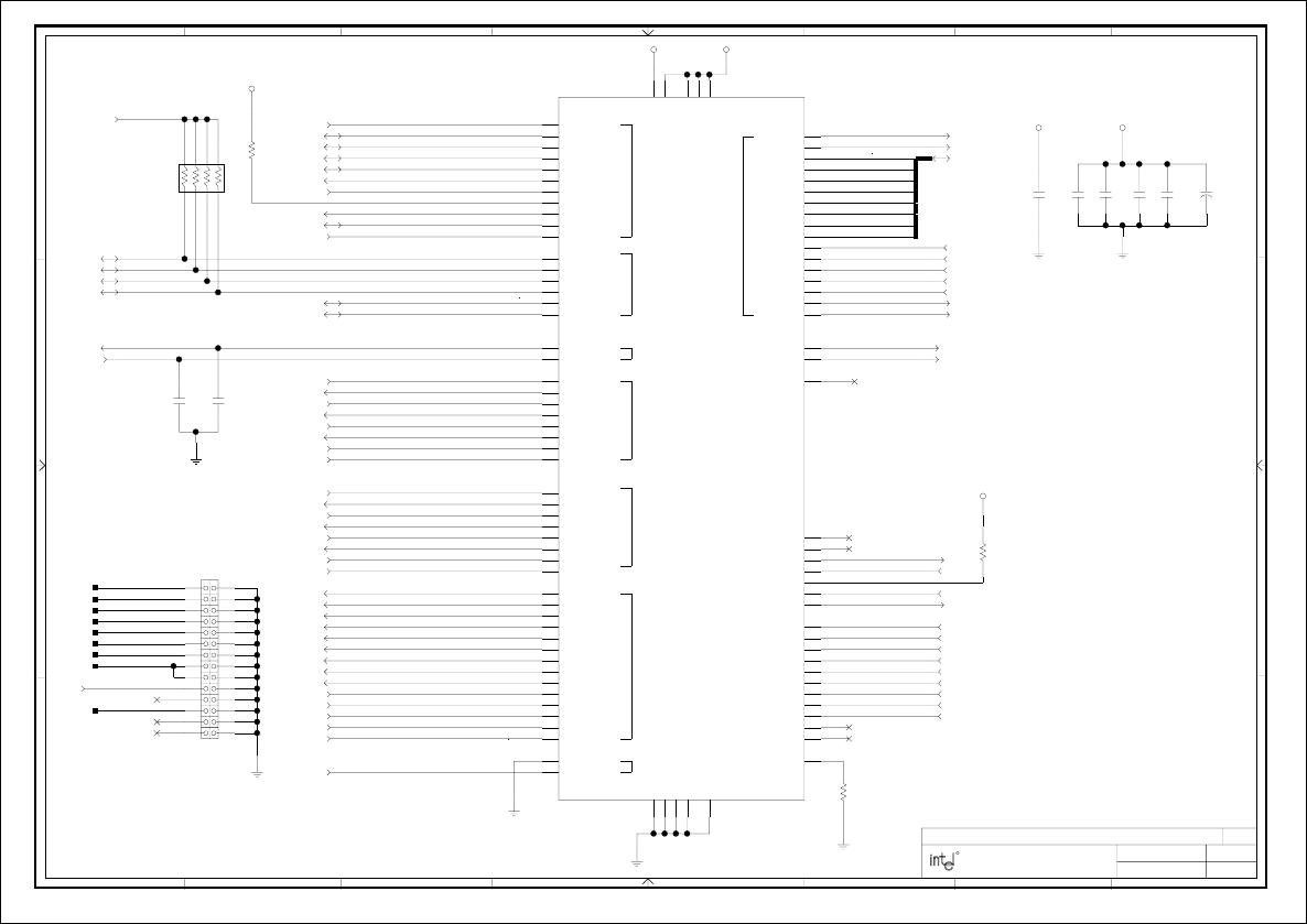
11-18-1999_10:46 12
SUPER I/O
R313
4.7K
KBCLK
26
9LPC_PME#
U17
27
18
45
44
15
11
10
93
65
53
96
85
14
83
9
67
77
30
95
84
98
87
92
90
16
17
78
75
74
73
72
71
70
69
6829
3
58
59
26
24
25
23
22
21
20
56
57
63
62
61
66
13
12
49
48
52
51
50
47
46
43
42
41
39
38
37
36
35
34
33
32
76
60
31
7
28
54
55
81
100
89
97
86
4
5
2
1
8
94
91
99
88
19
6
79
40
82
80
64
R312
4.7K
J20
2827
25 26
9
87
65
43
2423
2221
20
2
19
1817
1615
1413
1211
10
1
SIO_14MHZ
5
9,10,12 LAD3/FWH3
9,10,12 LAD1/FWH1
9,10,12 LAD0/FWH0
9,12 LDRQ#0
SIO_PCLK7
5,12
26 MDAT
MCLK
26
25 RXD0
25 TXD0
25 DSR#0
25 RTS#0
25 CTS#0
25 DTR#0
25 RI#0
25 DCD#0
25 RXD1
25 DSR#1
25 RTS#1
25 CTS#1
25 DTR#1
25 RI#1
25 DCD#1
26 MTR#0
26 DIR#
26 HDSEL#
26 INDEX#
26 TRK#0
24
SLIN#
26 RDATA#
24
PAR_INIT#
26 DSKCHG#
24
AFD#
24
STB#
24
SLCT
24
PE
24
BUSY
24
ACK#
24
ERR#
8,32 KBRST#
8,32 A20GATE
SERIRQ
8,12,21,32
18
PWM1
9
LPC_SMI#
27
MIDI_IN
27
MIDI_OUT
27
J1BUTTON1
27
J1BUTTON2
27
J2BUTTON1
27
J2BUTTON2
27
JOY1X
27
JOY1Y
27
JOY2X
27
JOY2Y
9,10,12 LAD2/FWH2
26 KBDAT
25 TXD1
18
TACH2
18
PWM2
26 DRVDEN#0
18
KEYLOCK#
26 DRVDEN#1
26 DS#0
26 STEP#
26 WDATA#
26 WGATE#
26 WRTPRT#
9,10,12 LAD3/FWH3
9,10,12 LAD2/FWH2
9,10,12 LAD1/FWH1
9,10,12 LAD0/FWH0
9,10,12 LFRAME#/FWH4
6,8,10,11,12,16,19,20,21,22 PCIRST#
5,12 SIO_PCLK7
9,12 LDRQ#0
8,12,21,32 SERIRQ
PDR7
PDR0
PDR1
PDR2
PDR3
PDR4
PDR5
PDR6 24
PDR[7:0]
18 IRRX
18 IRTX
6,8,10,11,12,16,19,20,21,22 PCIRST#
5,9 MULT1_GPIO
LPCPD#
SYSOPT
9,10,12 LFRAME#/FWH4
470PF
C320
470PF
C317
0.1UF
C309
0.1UF
C321C348
0.1UF
C313
0.1UF 0.1UF
C323
2.2UF
C349
2
1
26 VCC5_KBMS_J
4.7K
R315
RP5
4.7K
1234
5678
CPU_TACH1
PCD PLATFORM DESIGN
REV:
DRAWN BY:
LAST REVISED:
PROJECT:
SHEET:
FOLSOM, CALIFORNIA 95630
1900 PRAIRIE CITY ROAD
87654321
A
B
C
D
12345678
D
C
B
A
1.01
TITLE: INTEL(R) 820 CHIPSET CUSTOMER REFERENCE BOARD
OF 36
R
VCC3_3
SIO
LPC47B27X
A20GATE
ACK#
ALF#
AVSS
BUSY
CLKI32
CLOCKI
CTS1#
CTS2#
DCD1#
DCD2#
DIR#
DRVDEN0
DRVDEN1
DS0#
DSKCHG#
DSR1#
DSR2#
DTR1#
DTR2#
ERROR#
FAN1/GP33
FAN2/GP32
FDC_PP/DDRC/GP43
GND1
GND2
GND3
GND4
GP10/J1B1
GP11/J1B2
GP12/J2B1
GP13/J2B2
GP14/J1X
GP15/J1Y
GP16/J2X
GP17/J2Y
GP20/P17
GP21/P16
GP22/P12
GP25/MIDI_IN
GP26/MIDI_OUT
GP27/IO_SMI#
GP30/FAN_TACH2
GP31/FAN_TACH1
GP60/LED1
GP61/LED2
HDSEL#
INDEX#
INIT#
IRRX2/GP34
IRTX2/GP35
KBDRST
KCLK
KDAT
LAD0
LAD1
LAD2
LAD3
LDRQ#
LFRAME#
LRESET#
MCLK
MDAT
MTR0#
PCI_CLK PD0
PD1
PD2
PD3
PD4
PD5
PD6
PD7
PE
PME#
RDATA#
RI1#
RI2#
RTS1#
RTS2#
RXD1
RXD2_IRRX
SERIRQ
SLCT#
SLCTIN#
STEP#
STROBE#
TRK0#
TXD1
TXD2_IRTX
VCC1
VCC2
VCC3
WDATA#
WGATE#
WRTPRT#
VREF
GP24/SYSOPT
VTR
LPCPD#
SERIAL PORT 1
SERIAL PORT 2
FDC I/F
LPC I/F
INFRARED I/F
CLOCKS
KYBD/MSE I/F
PARALLEL PORT I/F
VCC3_3
VCC5
VCC5 VCC3_3
VCC3_3
+
Pulldown on SYSOPT for IO address of 0x02E
LPC header. For debug only.
Super I/O
Place decoupling caps near each power pin.Place next to VREF.
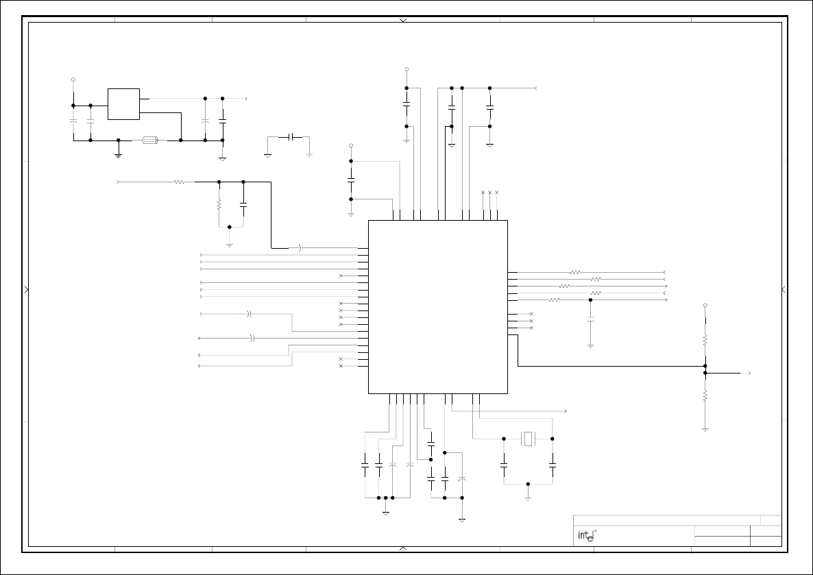
11-18-1999_10:46 13
AUDIO
13,14VCC5_AUDIO
AC_BITCLK 9,15
0.1UF
C358
PRI_DWN_RST# 15
9,15
AC_SDATAOUT
AC_SDATAIN0 9,15
AC_SYNC 9,15
R56
0K
R106
0K
R77
0K
RX3D_C
U2
3
2
28
27
17
16
10
5
8
33
11
13
12
44
43
40
37
22
21
41
39
36
35
24
23
31
32
7
4
9
1
34
46
45
47
48
20
18
19 6
42
26
38
25
15
14
30
29
14 CD_REF
14 LINE_IN_L
14 CD_L
14 CD_R
18 AC97_SPKR
14
AUD_VREFOUT
10K
R67
1K
R66
14 LINE_IN_R
24.576MHZ
Y1
21
14 MIC_IN
15 MONO_PHONE
100K
R28
14 LNLVL_OUT_L
13,14
VCC5_AUDIO
14 LNLVL_OUT_R
L17
21
AC97_SPKR_R
AC97_SPKR_C
MONO_PHONE_C
AFILT1_C
AFILT2_C
FILT_L_C
AC_XTAL_IN
AC_XTAL_OUT
AC_VREF_C
FILT_R_C
CX3D_C
R29
100K
0K R31
PRI_DWN_RST#_R
AC_SDATAOUT_R
AC_SDATAIN_R
AC_SYNC_R
AC_BITCLK_R
0K
R116
MONO_OUT_CMONO_OUT
15
0.1UF
C62
C83
10UF
1
2
C57
10UF
2
1
0.1UF
C85
1UF-TANT C70
21
0.1UF
C77
0.1UF
C49 C21
0.1UF
0.1UF
C76
1UF-TANT
C63 12
1UF-TANT
C12
21
C19
270PF-NPO
C18
270PF-NPO
22PF
C95
22PF C94
C7
1UF-TANT
1
2
1UF-TANT C1
2
1
C20
0.1UF
0.047UF
C17 C16
0.1UF
10UF-TANT
C9
1
2
0.1UF
C48
14EAPD
10PF
C84
VR2
1
3
4
PCD PLATFORM DESIGN
REV:
DRAWN BY:
LAST REVISED:
PROJECT:
SHEET:
FOLSOM, CALIFORNIA 95630
1900 PRAIRIE CITY ROAD
87654321
A
B
C
D
12345678
D
C
B
A
1.01
TITLE: INTEL(R) 820 CHIPSET CUSTOMER REFERENCE BOARD
OF 36
R
AGND
AGND
AFILT1
AFLIT2
AUX_L
AUX_R
AVDD1
AVDD2
AVSS1
AVSS2
BIT_CLK
CD_REF
CD_L
CD_R
CHAIN_CLK
EAPD
CS0
CS1
CX3D
DVDD1
DVDD2
DVSS1
DVSS2
FILT_L
FILT_R
LINE_IN_L
LINE_IN_R
LINE_OUT_L
LINE_OUT_R
LNLVL_OUT_L
LNLVL_OUT_R
MIC1
MIC2
MONO_OUT
NC40
NC43
NC44
PC_BEEP
PHONE
RESET#
RX3D
SDATA_IN
SDATA_OUT
SYNC
VIDEO_L
VIDEO_R
VREF
VREFOUT
XTL_IN
XTL_OUT
AD1881
AGND
AGND
VCC3_3
VCC3_3
VCC3_3
XTAL
AGND
VCC12
+
+
+
+
+
+
+
+
AGND
MC78M05CDT
VIN
+5V
GND
No stuff C84.
No stuff
No stuff
Series resistors are for test purposes only.
No stuff C358.
AC’97 Audio
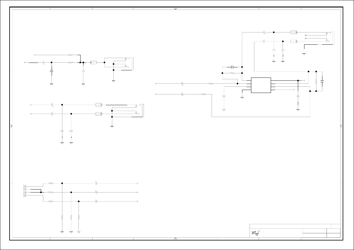
11-18-1999_10:47 14
AUDIO
LNLVL_L_R
13 LNLVL_OUT_L
R2
20K
R4
20K U1
8
7
6
5
1
2
3
4
13 MIC_IN
4.7K
R30
4.7K
R51
4.7K
R27
4.7K
R52
13
CD_R
13
CD_L
13
CD_REF
R18
4.7K
R25
4.7K
LINE_IN_R
13
LINE_IN_L
13
1K
R9
2.2K
R7
13VCC5_AUDIO
13 LNLVL_OUT_R
L5
21
L1
21
L4
12
MIC_IN_R MIC_IN_FB
LINE_IN_R_C
LINE_IN_L_C LINE_IN_L_FB
R1
20K
R3
20K
LNLVL_R_C
LNLVL_L_C
LNLVL_R_R
HP_OUTA
HP_OUTB
HP_OUTA_C
HP_OUTB_C
HP_OUTA_FB
HP_OUTB_FB
MIC_IN_C
13 AUD_VREFOUT
AC_BYPASS
L2
21
L3
12
LINE_IN_R_FB J5
LI25
LI23
LI24
LI22
LI21
J5
M16
M17
M19
M18
M20
CD_REF_J
CD_L_C
CD_REF_C
CD_R_C
J4
1
2
3
4
CD_L_J
CD_R_J
13EAPD
C23
1UF-TANT
12
1UF
C58 12
1UF
C59
21
C50
1UF
12
C13
1UF-TANT
21
C2
1UF
2
1
100UF
C10 21
C3
100UF
12
10PF-NPO
C24
1
2
C11
10PF-NPO
2
1
C6
1UF-TANT
12
0.01UF
C34
10PF-NPO
C28
2
1
C27
1UF-TANT
21
C26
10PF-NPO
1
2
10PF-NPO
C22
2
1
C25
1UF-TANT
21
100PF
C4
100PF
C8
J5
HP30
HP28
HP29
HP27
HP26
C14
0.1UF
1
2
PCD PLATFORM DESIGN
REV:
DRAWN BY:
LAST REVISED:
PROJECT:
SHEET:
FOLSOM, CALIFORNIA 95630
1900 PRAIRIE CITY ROAD
87654321
A
B
C
D
12345678
D
C
B
A
1.01
TITLE: INTEL(R) 820 CHIPSET CUSTOMER REFERENCE BOARD
OF 36
R
AGND
AGND
LM4880
OUTA
INA
BYPASS
GND
VDD
OUTB
INB
SHUTDN
AGND AGND
AGND
AGND
AGND AGND
AGNDAGND
AGNDAGND AGND
AGND
AGND
DB15_AUD_STK
DB15_AUD_STK
+
+
+
+
+
+
+
+
+
+
+
+
+
+
+
+
DB15_AUD_STK
+
Microphone Input
Stereo HP/Spkr out
AC’97 Audio
CD Analog Input
Line_In Analog Input
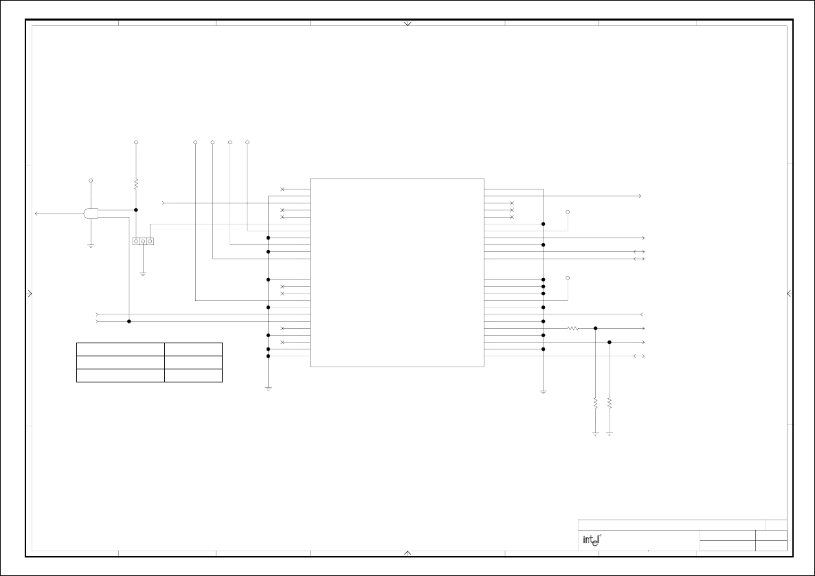
15
AUDIO/MODEM RISER
R125
10K
9,13
AC_BITCLK
9,13
AC_SYNC
13 MONO_OUT
9,13 AC_SDATAOUT
13MONO_PHONE
JP2
3
2
1
PRI_DWN#
PRI_DWN_U
R68
4.7K
23
AC97_USB+
23
AC97_USB-
9AC_RST#
U3
5
4
6
7
14
13
PRI_DWN_RST#
23
AC97_OC#
J8
A8
A11
A10
B6
A13
A5
A4
A3
B14
B13
B5
B4
A2
B3
A12
A9
A6
B22
B20
B16
B12
B10
B8
A22
A20
A18
A16
A14
B2
A1B1
A17B17
B19
B21
A19
A21
B18
B23 A23
B7 A7
B11
A15B15
B9
AC_SDATAIN1_R R113
AC_SDATAIN0 9,13
AC_SDATAIN1 9
R108
10K
PCD PLATFORM DESIGN
REV:
DRAWN BY:
LAST REVISED:
PROJECT:
SHEET:
FOLSOM, CALIFORNIA 95630
1900 PRAIRIE CITY ROAD
87654321
A
B
C
D
12345678
D
C
B
A
1.01
TITLE: INTEL(R) 820 CHIPSET CUSTOMER REFERENCE BOARD
OF 36
R
VCC12-VCC12
VCC3_3SBY
VCC3_3SBY
VCC3_3SBY
VCC5
VCC5VCC3_3
SN74LVC08A
AC’97_RISER
AMR_CONNECTOR
KEY
KEY
KEY
KEY
+12V
+3.3VD +3VDUAL/3VSBY
+5VD
+5VDUAL/5VSBY-12V
AC97_BITCLKAC97_MSTRCLK
AC97_RESET#
AC97_SDATA_IN0
AC97_SDATA_IN1
AC97_SDATA_IN2
AC97_SDATA_IN3
AC97_SDATA_OUT AC97_SYNC
AUDIO_MUTE# AUDIO_PWRDWN
(ISOLATED)GND[0]
GND[10]
GND[11]
GND[12]
GND[13]
GND[14]
GND[1]
GND[2]
GND[3]
GND[4]
GND[5]
GND[6]
GND[7]
GND[8]
GND[9]
MONO_OUT/PC_BEEP
MONO_PHONE
RESV[1]
RESV[2]
RESV[3]
RESV[4]
RESV[5]
RESV[6]
RESV[7]
S/P_DIF_IN
PRIMARY_DN#
USB+
USB-
USB_OC
0K
AC’97 Audio/Modem Riser
Audio Down JP2
Enable* 1-2
Disable 2-3
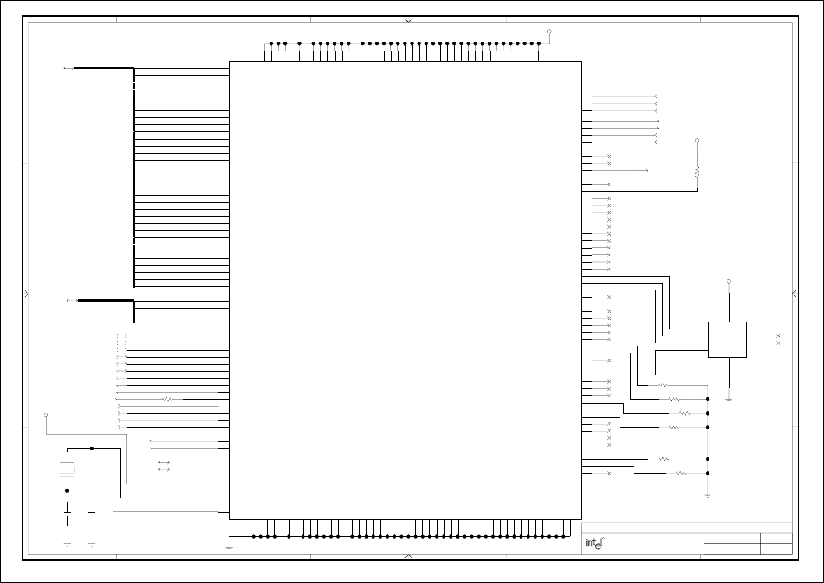
11-18-1999_10:48 16
LAN CONTROLLER
R15
619
TDN 17
8,19,20,21
PCI_PME#
8,20,21
AD[31:0]
AD3
AD4
AD5
AD6
AD7
AD8
AD9
AD10
AD11
AD12
AD13
AD14
AD15
AD16
AD17
AD18
AD19
AD20
AD21
AD22
AD23
AD24
AD25
AD26
AD27
AD28
AD29
AD30
AD31
AD2
AD1
AD0
C_BE#[3:0]
8,20,21 C_BE#0
C_BE#1
C_BE#2
C_BE#3
8,20,21,32 FRAME#
8,20,21,32 IRDY#
8,20,21,32 TRDY#
8,20,21,32 DEVSEL#
8,20,21,32 STOP#
8,20,21 PAR
8,19,20,21,32 PIRQ#A
8,20,21,32 PERR#
PGNT#3
8,32
5PCLK5
25MHZ
Y2
2
1
17
RDP
17
RDN
TDP 17
62K
R11
R14
3.3K
549
R16
R57
3.3K
6,8,10,11,12,19,20,21,22 PCIRST#
17 LAN_RSMRST#
3.3K
R58
3.3K
R59
7,9,29,31 PWROK
8,20,21,32 SERR#
AD20
8,16 PREQ#3
8,32 100
R75
U5
M13
M9
G2
N11
P11
L11
L6
H11
H10
H9
G11
G10
G9
G8
G7
F11
F10
F9
F8
F7
F6
F5
F4
E11
E10
E9
E8
E7
E6
E5
E4
D11
D8
D7
D6
D5
D4
L9
L10
L5
L4
K11
K10
K9
K8
K7
K6
K5
K4
J11
J10
J9
J8
J7
J6
J5
H8
H7
H6
H5
G6
G5
E12
P2
N6
K3
E1
A7
A3
N1
M6
K2
E2
B7
B3
C10
N12
P8
K12
G14
A11
P12
N8
K13
G13
C13
B11
C11
A12
C12
B13
B14
B12
D12
D14
D13
A13
C8
M8
N9
P7
F14
F13
F12
G12
H14
H13
H12
J14
J13
J12
K14
L14
L13
L12
M14
N14
P13
N13
M12
M11
P10
N10
M10
P9
A6
C5
B10
E14
E13
C14
C9
A10
A9
B9
G1
C2
J3
C3
A4
A2
J2
H2
J1
H1
H3
G3
F1
F2
C4
F3
L3
M4
B8
A8
C7
C6
B6
B5
A5
B4
B2
B1
C1
D3
D2
D1
E3
K1
L2
L1
M3
M2
M1
N2
N3
P3
N4
P4
M5
N5
P5
P6
M7
N7
AUXPWR
EEDI
EEDO
EESK
EECS
FLD5
FLD6
CLKRUN#_LAN
TEST_LAN
RBIAS10
RBIAS100
AD20_RLAN
LAN_X1
LAN_X2
XREF1=17SPEEDLED
17ACTLED
17LILED
U8
8
3
4
2
1
5
6
7
22PF
C101
22PF
C96
9,32 ALERTCLK_SBY
9,32 ALERTDATA_SBY
PCD PLATFORM DESIGN
REV:
DRAWN BY:
LAST REVISED:
PROJECT:
SHEET:
FOLSOM, CALIFORNIA 95630
1900 PRAIRIE CITY ROAD
87654321
A
B
C
D
12345678
D
C
B
A
1.01
TITLE: INTEL(R) 820 CHIPSET CUSTOMER REFERENCE BOARD
OF 36
R
VCC3_3SBY
VCC3_3SBY
XTAL
VCC3_3SBY
82559
AD0
AD1
AD2
AD3
AD4
AD5
AD6
AD7
AD8
AD9
AD10
AD11
AD12
AD13
AD14
AD15
AD16
AD17
AD18
AD19
AD20
AD21
AD22
AD23
AD24
AD25
AD26
AD27
AD28
AD29
AD30
AD31
C/BE0#
C/BE1#
C/BE2#
C/BE3#
FRAME#
IRDY#
TRDY#
DEVSEL#
STOP#
PAR
INTA#
PERR#
SERR#
IDSEL
REQ#
GNT#
RST#
CLK
ISOLATE#
ALTRST#
SMBCLK
SMBD
TDN
RDP
RDN
SMBALRT#
CSTSCHG
PME#
FLA16
FLA15/EESK
FLA14/EEDO
FLA13/EEDI
FLA12/MCNTSM#
FLA11/MINT
FLA10/MRING#
FLA9/MRST
FLA8/IOCHRDY
FLA6
FLA5
FLA4
FLA3
FLA2
FLA1/AUXPWR
FLA0/PCIMODE#
FLD7
FLD6
FLD5
FLD4
FLD3
FLD2
FLD1
FLD0
EECS
FLCS#
FLOE#
CLKRUN#
TEST
TEXEC
TCK
TI
TO
RBIAS10
RBIAS100
VREF
LILED
ACTLED
SPEEDLED
TDP
VCCPL[0]
VCCPL[1]
VCCPL[2]
VCCPL[3]
VCCPT
VSSPL[0]
VSSPL[1]
VSSPL[2]
VSSPL[3]
VSSPT
VSSPP[0]
VSSPP[1]
VSSPP[2]
VSSPP[3]
VSSPP[4]
VSSPP[5]
VCCPP[0]
VCCPP[1]
VCCPP[2]
VCCPP[3]
VCCPP[4]
VCCPP[5]
VCC[0]
VCC[1]
VCC[2]
VCC[3]
VCC[4]
VCC[5]
VCC[6]
VCC[7]
VCC[8]
VCC[9]
VCC[10]
VCC[11]
VCC[12]
VCC[13]
VCC[14]
VCC[15]
VCC[16]
VCC[17]
VCC[18]
VCC[19]
VCC[20]
VCC[21]
VCC[22]
VCC[23]
VCC[25]
VCC[24]
VSS[0]
VSS[1]
VSS[2]
VSS[3]
VSS[4]
VSS[5]
VSS[6]
VSS[7]
VSS[8]
VSS[9]
VSS[10]
VSS[11]
VSS[12]
VSS[13]
VSS[14]
VSS[15]
VSS[16]
VSS[17]
VSS[18]
VSS[19]
VSS[20]
VSS[21]
VSS[22]
VSS[23]
VSS[24]
VSS[25]
VSS[26]
VSS[27]
VSS[28]
VSS[29]
VSS[30]
VSS[31]
X2
X1
VIO
FLWE#
FLA7
NC2
NC1
GND
EECS
EESK
EEDO
EEDI VCC
93C46
VCC5SBY
LAN
No stuff R57, R58
1711-18-1999_10:48
16,17
LILED
16,17
ACTLED
330
R61
R64
330
LILED
16,17
ACTLED
16,17
SPEEDLED
16
LI_J
ACT_J
SPEED_J
JP1
JP4
JP3
R60
330
330
R73
330
R78
16 LAN_RSMRST#
9,31 RSMRST#
TDN
16
16 TDP
J17
3
2
1
RJ4_J
TXC_J
RJ_7_J
RXC_J
LI_CR
ACT_CR
49.9-1%
R26
49.9-1%
R20
75
R6
75
R5
75
R8
75
R10
49.9-1%
R62
49.9-1%
R63
16 RDP
16 RDN
XC_R
TD_C
RD_C
0.1UF
C61
0.1UF
C79
C31
0.1UF
470PF
C5
J2
15
16
13
14
1
2
6
5
4
3
8
11
7
9
12
10
18
17
RDC_J
TDC_J
0.1UF
C78
PCD PLATFORM DESIGN
REV:
DRAWN BY:
LAST REVISED:
PROJECT:
SHEET:
FOLSOM, CALIFORNIA 95630
1900 PRAIRIE CITY ROAD
87654321
A
B
C
D
12345678
D
C
B
A
1.01
TITLE: INTEL(R) 820 CHIPSET CUSTOMER REFERENCE BOARD
OF 36
R
VCC3_3 VCC3_3
RJMAG
SHLD1
SHLD2
TD+
TD-
RD+
RD-
TDC
RDC
RJ-4
RJ-5
RJ-7
RJ-8
TXC
RXC
RJ-45
LAN
LAN
For debug only. Hold LAN in reset.
Place termination resistors close to 82559. No stuff JP1,JP3,JP4,R60,R73,R78.
No stuff C61, C79.
No stuff C31.
C5 must be rated at 1500V.
No stuff C5.
82559 LAN J17
Enable* 1-2
Disable 2-3
11-18-1999_10:49
SYSTEM
18
GPIO23_FPLED9
U14
14
7
56
U14
43
7
14
R253
330
IRRX
12
1M
R252
SP1
1
2
22 IDEACTS#
22 IDEACTP#
R345
10K
R344
10K
R352
68
R353
68
JP24
1
2
3
JP23
3
2
1
R326
4.7K
JP22
3
2
1
4.7K
R316
12
PWM1
R329
4.7K
R350
2.2K
9SPKR
P_BEEP
JP25
3
2
113
AC97_SPKR
IDE_ACTIVE
9
PWRBTN#
12
TACH2
R257
0K
82
R357
12 IRTX
J25
26
25
24
23
22
21
20
19
18
17
16
15
14
13
12
11
10
9
8
7
6
5
4
3
2
1
470
R356
R358
4.7K
KEYLOCK#
12
R355
220
R289
330
CR7
2
1
IRTX_R
HDLED_R
PLED_R
PWRBTN_FP#
SPKR_FP
SPKR_Q
SPKR_ONBOARD
SBY_LED_CR
PC_BEEP
U19
89
7
14
U19
14
7
12
DUAL_COLOR
CR6
12
LED_PU0 LED_PU1
9GPIO26_FPLED
330
R246
4.7K
R234
C267
1UF
470PF
C354
470PF
C355
R359
100K
0.1UF
C327
C316
0.1UF
10K
R354
C322
0.1UF
C350
0.1UF 50V
2
1
C356
10UF 16V
1
2
0.1UF
C353
MMBT3904LT1
Q15
E
C
B
12
PWM2
SW1
PCD PLATFORM DESIGN
REV:
DRAWN BY:
LAST REVISED:
PROJECT:
SHEET:
FOLSOM, CALIFORNIA 95630
1900 PRAIRIE CITY ROAD
87654321
A
B
C
D
12345678
D
C
B
A
1.01
TITLE: INTEL(R) 820 CHIPSET CUSTOMER REFERENCE BOARD
OF 36
R
SN74LVC07A
GND
VCC
VCC3_3SBYVCC3_3SBY
SN74LVC07A GND
VCC
VCC3_3
VCC3_3SBY
VCC5
VCC3_3SBY
VCC3_3
VCC3_3
VCC3_3
VCC5
NEG
POS
+
VCC5
VCC5
VCC12
VCC12
VCC12
VCC3_3
FNT_PNL_CONN
VCC3_3
VCC5
VCC3_3
SN74LVC07A GND
VCC
VCC3_3SBY
SN74LVC07A GND
VCC
VCC3_3SBY
+
+
13
2
KEY
KEY
No stuff.
For test only
No stuff.
KEY
INFRARED
H.D. LED
PWM1
TACH2
PWM2
SPEAKER
POWER SW.
For test only
ICH has internal pullup and debounce on PWRBTN#
KEY
Speaker Circuit
KEY
KEY
KEYLOCK
POWER LED
Onboard LED indicates the standby well is on
PWM outputs from SIO need power buffers for driving fan inputs.
to prevent hot swapping memory.
For debug only.
System
Onboard Spkr JP25
Enable* 2-3
Disable 1-2
11-18-1999_10:49
AGP CONNECTOR
19
J13
B42
B24
A66B66
B65
B64
B63
B62
B61
B60
B59
B58
B57
B56
B55
B54
B53
B52
B51
B50
A65
A64
A63
A62
A61
A60
A59
A58
A57
A56
A55
A54
A53
A52
A51
A50
B49
B48
A49
A48
A47
A46
A45
A44
A43
A42
A41
B47
B46
B45
B44
B43
B41
A35
A36
A37
A38
A39
A40B40
B39
B38
B37
B36
B35
B34 A34
A33
A32
A31
A30
A29
A28
A27
A26
B33
B32
B31
B30
B29
B28
B27
B26
B16
B25 A25
A24
B23
B22
A23
A22
B21 A21
A20
A19
A18
A17
A16
A15
A14
A13
A12
B14
A11
A10
A9
A8
A7
A6
A5
A4
A3
A2
A1
B20
B19
B18
B17
B15
B13
B12
B11
B10
B9
B8
B7
B6
B5
B4
B3
B2
B1
19,29 TYPEDET#
R208
200-1%
7 GAD[31:0]
GAD0
GAD2
GAD4
GAD6
GAD9
GAD11
GAD13
GAD15
GAD16
GAD18
GAD20
GAD22
GAD24
GAD26
GAD28
GAD30
GAD1
GAD3
GAD5
GAD7
GAD8
GAD10
GAD12
GAD14
GAD17
GAD19
GAD21
GAD23
GAD25
GAD27
GAD29
GAD31
23 AGP_OC#
5AGPCLK_CONN
7,32 GREQ#
ST0 ST1
ST2
7ST[2:0]
7,32 RBF#
SBA0
SBA2
SBA4
SBA6
SBA5
SBA7
SBA3
SBA1
7
SBA[7:0]
7,32 SBSTB
7,32 ADSTB1
GC/BE#2
GC/BE#0
GC/BE#3
GC/BE#1
7 GC/BE#[3:0]
7,32 GIRDY#
7,32 GDEVSEL#
32 GPERR#
32 GSERR#
7,32 ADSTB0 7,32ADSTB#0
7,32GPAR
8,16,20,21
PCI_PME# 7,32
GSTOP# 7,32
GTRDY#
7,32
GFRAME#
7,32
ADSTB#1
7,32
SBSTB#
7,32
WBF#
7,32
PIPE#
7,32
GGNT# 6,8,10,11,12,16,20,21,22
PCIRST#
23
USBAGP-
19,29
TYPEDET#
8,16,20,21,32
PIRQ#A
8,20,21,32 PIRQ#B
R193
301-1%
23 USBAGP+
6MCH_AGPREF
6
CONN_AGPREF
CON_AGPREF_Q
Q8
2
3
1
PCD PLATFORM DESIGN
REV:
DRAWN BY:
LAST REVISED:
PROJECT:
SHEET:
FOLSOM, CALIFORNIA 95630
1900 PRAIRIE CITY ROAD
87654321
A
B
C
D
12345678
D
C
B
A
1.01
TITLE: INTEL(R) 820 CHIPSET CUSTOMER REFERENCE BOARD
OF 36
R
AGP4XU_20
OVRCNT#
5V_A
5V_B
USB+
GND_K
INTB#
CLK
REQ#
VCC3_3_F
ST0
ST2
RBF#
GND_L
SBA0
SBA2
SB_STB
GND_M
SBA4
12V
TYPEDET#
RESV_A
USB-
GND_A
INTA#
RST#
GNT#
VCC3_3_A
ST1
RESV_B
RESV_H
PIPE#
GND_B
WBF#
SBA1
VCC3_3_B
SBA3
SB_STB#
GND_C
SBA5
SBA7
SBA6
RESV_C
GND_D
RESV
GND_N
RESV_D
VCC3_3_C
VCC3_3_H
VCC3_3_G
AD31
AD29
VCC3_3_I
AD27
AD25
GND_O
AD_STB1
AD23
AD30
AD28
VCC3_3_D
AD26
AD24
GND_E
AD_STB1#
C/BE3#
VDDQ_A
VDDQ_F
AD21
AD19
GND_P
AD17
C/BE2#
VDDQ_G VDDQ_B
AD16
AD18
GND_F
AD20
AD22
IRDY#
GND_Q
RESV_K
VCC3_3_J
DEVSEL#
VDDQ_H
FRAME#
RESV_E
GND_G
RESV_F
VCC3_3_E
TRDY#
STOP#
PME#
GND_H
PERR#
GND_R
PAR
AD15
VDDQ_C
AD13
AD11
GND_I
AD9
C/BE0#
VDDQ_D
AD_STB0#
AD6
GND_J
AD4
AD2
VDDQ_E
AD0
SERR#
C/BE1#
VDDQ_I
AD14
AD12
GND_S
AD10
AD8
VDDQ_J
AD_STB0
AD7
GND_T
AD5
AD3
VDDQ_K
AD1
VREF_CG VREF_GC
3_3VAUX1
3_3VAUX2
VDDQ
VDDQ
VCC3_3 VCC12
VCC3_3SBY
VCC5
2N7002LT1
1
3
2
AGPREF circuitry should be placed close to MCH.
AGP Connector
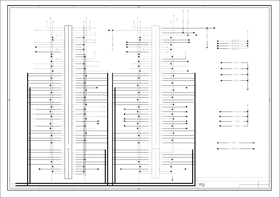
PCI CONNECTORS 1 AND 2
11-18-1999_10:50 20
J9
A2
A21
A27
A33
A39
A45
B25
B31
B36
B43
A53
B54
A5
A8
A10
A16
B5
B6
A59
A61
A62
B59
B61
B62
B19
B1
B60
A58B58
B48
A47B47
A46
B45
A44
A32B32
A31
B30
A57
A29B29
A28
B27
A25
B24
A23B23
A22
B21
B56
A20B20
A55B55
A54
B53
B52
A49
A52
B44
B33
B26
B16
A9
B37
A34
A12
A13
A18
A24
A30
A35
A37
A42
A48
B3
B12
B13
B15
B17
B22
B34
B38
B46
B49
A56
B57
B28
A17
A26
A6
B7 A7
B8
B35
B39
A43
B40
A19
B9
B11
B2
B4 A4
A3
A1
B18
A60
A11
A14
B10
B14
A15
A41
A40
B42
A38
A36
B41
20,21 PTCK
8,19,20,21,32 PIRQ#B
8,20,21,32 PIRQ#D
5PCLK1
8,32 PREQ#0
C_BE#1
C_BE#0
C_BE#2
C_BE#3
C_BE#0
C_BE#3
C_BE#2
C_BE#1
8,16,21 C_BE#[3:0]
8,16,20,21,32 IRDY#
8,16,20,21,32 DEVSEL#
8,20,21,32 PLOCK#
8,16,20,21,32 SERR#
8,16,20,21PAR
8,16,20,21,32
TRDY#
8,16,20,21,32
FRAME#
8,20,21,32
PIRQ#C 8,16,19,20,21,32
PIRQ#A
20,21
PTDI 20,21
PTMS 20,21 PTCK
8,32
PGNT#1
8,32 PREQ#1
5PCLK2
20 SDONEP1
20 SDONEP2
20 SBOP1
20 SBOP2
20 PRSNT#11
20 PRSNT#12
20 PRSNT#21
20 PRSNT#22
20 PU1_ACK64#
20 PU1_REQ64#
20 PU2_ACK64#
20 PU2_REQ64#
20
R_AD16
20
R_AD17
20,21
PTRST#
5.6K
R74
5.6K
R76
5.6K
R79
5.6K
R72
100
R120
100
R119
5.6K
RP12 8
7
6
54
3
2
1
2.7K
R178
2.7K
R179
2.7K
R176
2.7K
R177
20,21
PTDI 20,21
PTMS
8,16,20,21,32
STOP#
8,16,19,20,21PCI_PME#
6,8,10,11,12,16,19,20,21,22
PCIRST#
8,32
PGNT#0
20
R_AD17
20 PRSNT#11
20 PRSNT#12
8,16,20,21,32 PERR#
20
SBOP1 20
SDONEP1
IRDY#
DEVSEL#
PLOCK#
SERR#
20
R_AD16
20,21
PTRST#
20 PRSNT#21
20 PRSNT#22
6,8,10,11,12,16,19,20,21,22
PCIRST#
8,16,19,20,21
PCI_PME#
FRAME#
TRDY#
STOP#
SDONEP2
SBOP2
PAR
8,16 AD16
8,16 AD17
PERR#
8,19,20,21,32
PIRQ#B
8,20,21,32
PIRQ#D
8,20,21,32 PIRQ#C
8,16,19,20,21,32 PIRQ#A
AD25
8,16,21 AD[31:0]
AD30
AD3
AD5
AD7
AD17
AD31
AD29
AD27
AD25
AD23
AD19
AD14
AD12
AD10
AD8
AD1
AD2
AD4
AD6
AD9
AD11
AD13
AD15
AD16
AD18
AD20
AD22
AD24
AD26
AD30
AD28
AD0AD0
AD28
AD26
AD24
AD22
AD20
AD18
AD13
AD11
AD9
AD6
AD4
AD2
AD1
AD10
AD12
AD14
AD19
AD21
AD23
AD27
AD29
AD31
AD17
AD7
AD5
AD3
AD8
AD16
AD15
AD21
20
PU2_REQ64#
20 PU2_ACK64#
20
PU1_REQ64#
20 PU1_ACK64#
0.1UF
C117
0.1UF
C123
0.1UF
C113
0.1UF
C122
J10
B41
A36
A38
B42
A40
A41
A15
B14
B10
A14
A11
A60
B18
A1
A3
A4B4
B2
B11
B9
A19
B40
A43
B39
B35
B8
A7B7
A6
A26
A17
B28
B57
A56
B49
B46
B38
B34
B22
B17
B15
B13
B12
B3
A48
A42
A37
A35
A30
A24
A18
A13
A12
A34
B37
A9
B16
B26
B33
B44
A52
A49
B52
B53
A54
B55 A55
B20 A20
B56
B21
A22
B23 A23
B24
A25
B27
A28
B29 A29
A57
B30
A31
B32 A32
A44
B45
A46
B47 A47
B48
B58 A58
B60
B1
B19
B62
B61
B59
A62
A61
A59
B6
B5
A16
A10
A8
A5
B54
A53
B43
B36
B31
B25
A45
A39
A33
A27
A21
A2
PCD PLATFORM DESIGN
REV:
DRAWN BY:
LAST REVISED:
PROJECT:
SHEET:
FOLSOM, CALIFORNIA 95630
1900 PRAIRIE CITY ROAD
87654321
A
B
C
D
12345678
D
C
B
A
1.01
TITLE: INTEL(R) 820 CHIPSET CUSTOMER REFERENCE BOARD
OF 36
R
PCI3_CON
key
VCC3_3SBY
VCC5
VCC5VCC5
VCC5VCC5VCC5VCC5VCC12-
VCC3_3 VCC3_3
VCC12
VCC3_3
VCC12-
VCC12
VCC3_3
VCC5
VCC3_3SBY
PCI3_CON
key
PCI Slot 0
For pullups, see 4.3.3 of PCI 2.1 Specification
PCI Slot 1
0 and 1
PCI Connectors
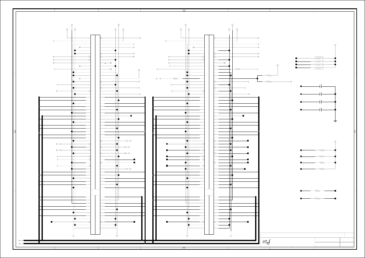
PCI CONNECTORS 3 AND 4
11-9-1999_11:43 21
J11
A2
A21
A27
A33
A39
A45
B25
B31
B36
B43
A53
B54
A5
A8
A10
A16
B5
B6
A59
A61
A62
B59
B61
B62
B19
B1
B60
A58B58
B48
A47B47
A46
B45
A44
A32B32
A31
B30
A57
A29B29
A28
B27
A25
B24
A23B23
A22
B21
B56
A20B20
A55B55
A54
B53
B52
A49
A52
B44
B33
B26
B16
A9
B37
A34
A12
A13
A18
A24
A30
A35
A37
A42
A48
B3
B12
B13
B15
B17
B22
B34
B38
B46
B49
A56
B57
B28
A17
A26
A6
B7 A7
B8
B35
B39
A43
B40
A19
B9
B11
B2
B4 A4
A3
A1
B18
A60
A11
A14
B10
B14
A15
A41
A40
B42
A38
A36
B41
J12
B41
A36
A38
B42
A40
A41
A15
B14
B10
A14
A11
A60
B18
A1
A3
A4B4
B2
B11
B9
A19
B40
A43
B39
B35
B8
A7B7
A6
A26
A17
B28
B57
A56
B49
B46
B38
B34
B22
B17
B15
B13
B12
B3
A48
A42
A37
A35
A30
A24
A18
A13
A12
A34
B37
A9
B16
B26
B33
B44
A52
A49
B52
B53
A54
B55 A55
B20 A20
B56
B21
A22
B23 A23
B24
A25
B27
A28
B29 A29
A57
B30
A31
B32 A32
A44
B45
A46
B47 A47
B48
B58 A58
B60
B1
B19
B62
B61
B59
A62
A61
A59
B6
B5
A16
A10
A8
A5
B54
A53
B43
B36
B31
B25
A45
A39
A33
A27
A21
A2
VAUX_JP
R110
R107
SDONEP3
21 SDONEP4
21 SBOP3
21 SBOP4
21
PRSNT#31
21
PRSNT#32
21
PRSNT#41
21
PRSNT#42
21
PU3_ACK64#
21
PU3_REQ64#
21
PU4_ACK64#
21
PU4_REQ64#
21
AD23
8,16
AD22
8,16
R_AD23 21
R_AD22 21
5PCLK4
21
R_AD22
PCIRST# 6,8,10,11,12,16,19,20,21,22
FRAME# 8,16,20,21,32
PTCK
20,21
PCLK3
5
IRDY#
8,16,20,21,32
DEVSEL#
8,16,20,21,32
PLOCK#
8,20,21,32 PERR#
8,16,20,21,32
SERR#
8,16,20,21,32
STOP# 8,16,20,21,32
TRDY# 8,16,20,21,32
PCI_PME# 8,16,19,20,21
C_BE#[3:0]8,16,20
C_BE#3
C_BE#2
C_BE#1
C_BE#0C_BE#0
C_BE#1
C_BE#2
C_BE#3
R118
100
R117
100
RP13
5.6K
8
7
6
54
3
2
1
R174
2.7K
R175
2.7K
R172
2.7K
R173
2.7K
PTMS 20,21
PTRST# 20,21
PTDI 20,21
PRSNT#31
21
PRSNT#32
21
PAR 8,16,20,21
SBOP3 21
SDONEP3 21
8,20,21,32 PIRQ#D
8,19,20,21,32 PIRQ#B
21 PRSNT#41
21 PRSNT#42
20,21
PTRST#
6,8,10,11,12,16,19,20,21,22
PCIRST#
8,16,19,20,21
PCI_PME#
IRDY#
DEVSEL#
PLOCK#
PERR#
SERR#
PAR
21
SBOP4 21
SDONEP4
STOP#
TRDY#
FRAME#
8,16,19,20,21,32
PIRQ#A 8,20,21,32
PIRQ#C
20,21
PTDI 20,21
PTMS
20,21 PTCK
PREQ#2
8,32
8,32
PGNT#2
PIRQ#B
8,19,20,21,32
PIRQ#D 8,20,21,32
PIRQ#A
8,16,19,20,21,32 PIRQ#C
8,20,21,32
8,32
PGNT#5
8,32 PREQ#5
8,12,32 SERIRQ
AD[31:0]8,16,20
AD3
AD0
AD28
AD30
AD26
AD24
AD22
AD20
AD18
AD16
AD13
AD11
AD9
AD6
AD4
AD2
AD3
AD5
AD7
AD17
AD31
AD29
AD27
AD25
AD23
AD21
AD19
AD14
AD12
AD10
AD8
AD1
AD2
AD4
AD6
AD9
AD11
AD13
AD15
AD16
AD18
AD20
AD22
AD26
AD28
AD0AD1
AD8
AD10
AD12
AD14
AD19
AD21
AD23
AD25
AD27
AD29
AD31
AD17
AD7
AD5
AD30
AD15
AD24
R255
8,32GNT#A
8,32REQ#A
R_AD23 21
GNT#A_R
SERIRQ_R
R99
21 PU3_ACK64# 21
PU3_REQ64# 21 PU4_ACK64# 21
PU4_REQ64#
C112 0.1UF
C121 0.1UF
C116 0.1UF
C126 0.1UF
9PCI_TEST
PCI3_CON
key
PCI3_CON
key
PCD PLATFORM DESIGN
REV:
DRAWN BY:
LAST REVISED:
PROJECT:
SHEET:
FOLSOM, CALIFORNIA 95630
1900 PRAIRIE CITY ROAD
87654321
A
B
C
D
12345678
D
C
B
A
1.0
TITLE: INTEL(R) 820 CHIPSET - FCPGA REFERENCE BOARD
OF 37
R
0K
0K
VCC5
VCC5
VCC12
VCC3_3
VCC5VCC5VCC12-VCC12-
VCC3_3
VCC5 VCC5
VCC3_3
VCC12
VCC3_3
VCC3_3SBY
0K
VCC3_3SBY
0K
PCI Slot 2 PCI Slot 3
GNT#A for debug only
J9 must be furthest from the processor.
2 and 3
PCI Connectors
SERIRQ for debug only
REQ#A for debug only
No Stuff R110.
PCI_TEST for debug only
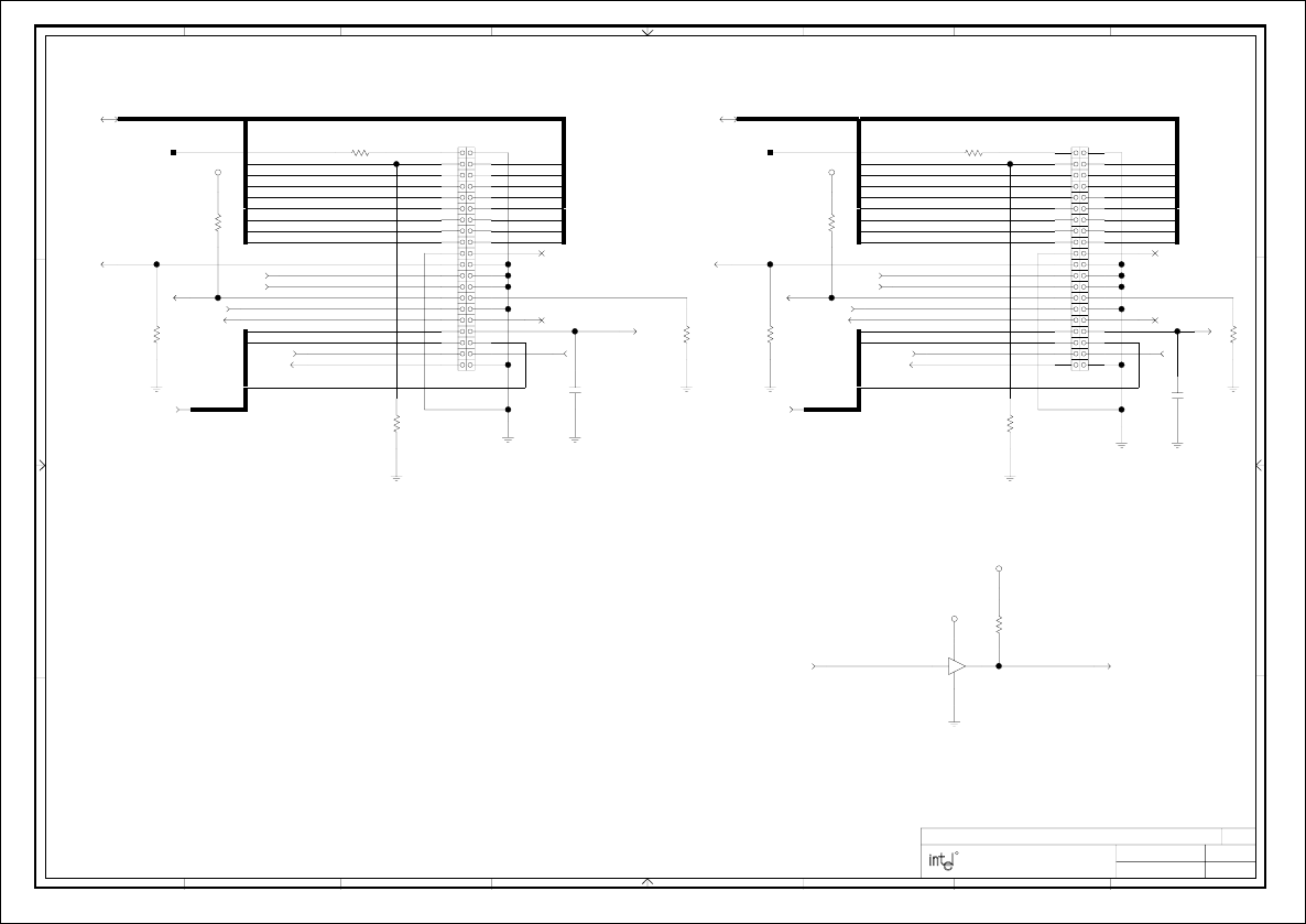
11-18-1999_10:51
IDE CONNECTORS
22
10S66DETECT
C318
0.047UF
10P66DETECT
22
PCIRST_BUF#
6,8,10,11,12,16,19,20,21 PCIRST#
9SDCS#1
8,32 IRQ15
9PDREQ
9PIORDY
8,32 IRQ14
9PDCS#1
9PDIOW# 9SDIOW#
9SDIOR#
9SDREQ
33
R333
1K
R336
5.6K
R335
10K
R334
470
R337
1K
R321
33
R318
5.6K
R320
10K
R319
470
R322
9
SDCS#3
9
PDCS#3
9PDD[15:0]
PDD8
PDD9
PDD10
PDD11
PDD12
PDD13
PDD14
PDD15
PDD1
PDD0
PDD2
PDD3
PDD4
PDD5
PDD6
PDD7
9SDA[2:0]
SDA2
SDA0
SDA1
9SDD[15:0]
SDD9
SDD10
SDD11
SDD12
SDD13
SDD14
SDD15
SDD1
SDD0
SDD2
SDD3
SDD4
SDD5
SDD6
SDD7 SDD8
22 PCIRST_BUF#
J22
9
87
65
40
4
39
3837
3635
3433
3231
30
3
29
2827
2625
2423
2221
20
2
19
1817
1615
1413
1211
10
1
J21
1
10
11 12
13 14
15 16
17 18
19
2
20
21 22
23 24
25 26
27 28
29
3
30
31 32
33 34
35 36
37 38
39
4
40
56
78
9
22 PCIRST_BUF#
8.2K
R351
18 IDEACTP#
PDA2
PDA1
9 PDA[2:0]
PDA0
18 IDEACTS#
9PDIOR#
9PDDACK# 9SIORDY
9SDDACK#
PCIRST#_RS
IDE_JSIDE_JP
PCIRST#_RP
U19
56
7
14
C329
0.047UF
PCD PLATFORM DESIGN
REV:
DRAWN BY:
LAST REVISED:
PROJECT:
SHEET:
FOLSOM, CALIFORNIA 95630
1900 PRAIRIE CITY ROAD
87654321
A
B
C
D
12345678
D
C
B
A
1.01
TITLE: INTEL(R) 820 CHIPSET CUSTOMER REFERENCE BOARD
OF 36
R
VCC5VCC5
VCC3_3
VCC3_3
SN74LVC07A GND
VCC
Secondary IDE
Primary IDE
For drive side detection, stuff C329,C318.
For host side detection, no stuff C329,C318.
P66DETECT and S66DETECT can be connected to a GPI for BIOS cable detection.
IDE Connectors
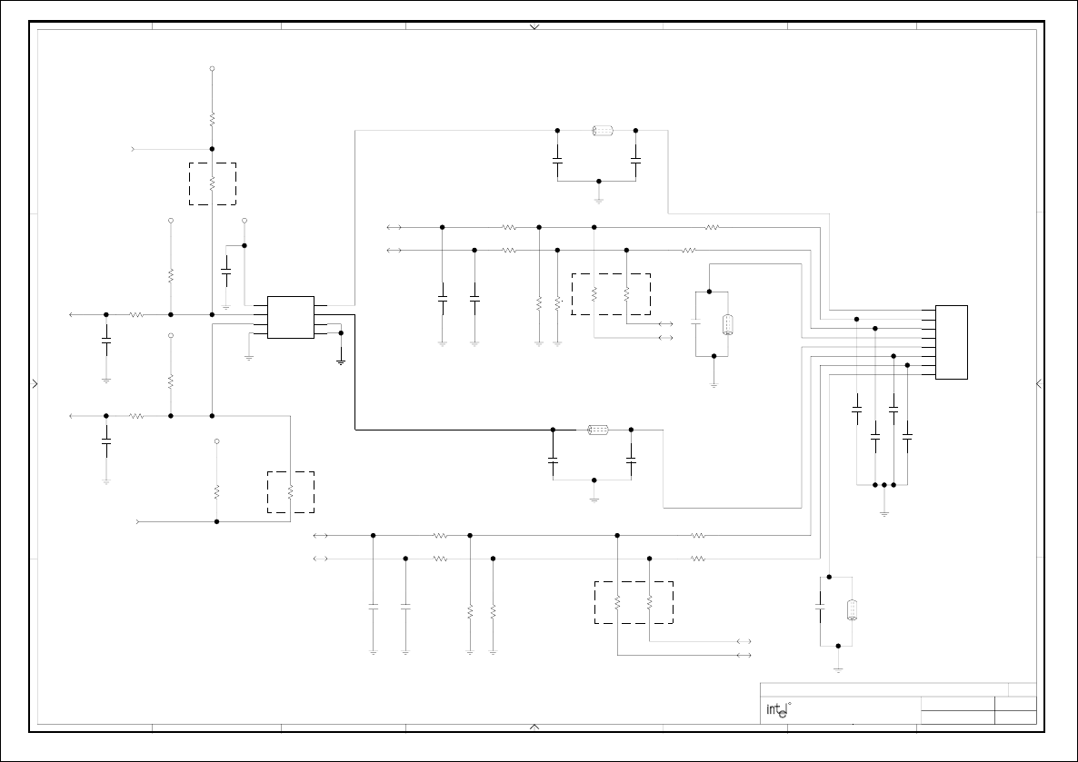
11-18-1999_10:57
USB CONNECTORS
23
R502
0K
USBV0
USBG0
USBV1
USBD1N
USBD1P
USBG1
10K
R97
9OC#0
R83
330K
AC97_OC#
15
R48
0K
R50
0K
USBP1N_R
USBP1P_R
4.7K
R91
19
USBAGP+
R41
0K
R42
0K
9USBP0N
9USBP0P
9USBP1P
15
R244
15K
R45
15K
R43
AGP_OC#
19
R92
330K
19
USBAGP-
15
R243 R46
0K
0K
R44
L11 12
L10
21
L7
2
1
L6
1
2
U7
4
3
6
7
8
2
1
5
USBPWR2_F
R49
15K
15AC97_USB-
15
AC97_USB+
R82
0K
9USBP1N
R86
4.7K
10K
R87
9OC#1
OC#0_RC
OC#1_RC
USBPWR1_F
USB_STK
J3
7
6
5
4
3
2
8
1
C120
0.1UF
0.1UF
C102
C109
0.1UF
C239
47PF 47PF
C241
68UF-TANT
C99
0.1UF
C44
47PF
C42
47PF
C41
47PF
C40
C39 47PF
68UF-TANT
C98
0.1UF
C43
470PF
C37
C38
470PF
47PF
C244
47PF
C245
15K
R47
R88
0K
R240
15-1%
R242
15-1%
USBD0N
USBD0PUSBD0P_R
USBD0N_R R501
0K
PCD PLATFORM DESIGN
REV:
DRAWN BY:
LAST REVISED:
PROJECT:
SHEET:
FOLSOM, CALIFORNIA 95630
1900 PRAIRIE CITY ROAD
87654321
A
B
C
D
12345678
D
C
B
A
1.01
TITLE: INTEL(R) 820 CHIPSET CUSTOMER REFERENCE BOARD
OF 36
R
VCC3_3
VCC3_3 OC#2
GND
IN
OC#1
OUT1
OUT2
EN#1
EN#2
TPS2042
VCC3_3
VCC5VCC3_3
VCC0
GND1
DATA0-
DATA0+
GND0
VCC1
DATA1-
DATA1+
Place caps close to connector.
Do Not
Stuff
15 ohm resistors and 47pf caps should be within 1" of ICH
Do Not
Stuff
Do Not
Stuff
Do Not
Stuff
C98, C99 must have low ESR.
USB Connectors
C39-C42 for test and debug only.
11-18-1999_11:22
PARALLEL PORT
24
PDR7_R
PDR6_R
PDR5_R
PDR4_R
PDR3_R
SLIN#_R
PDR2_R
PAR_INIT#_R
VCC5_DB25_CR
SLCT
12
PE
12
BUSY
12
ACK#
12
SLIN#
12
J6
P15
P16
P13
P23
P10
P25
P12
P24
P11
P22
P9
P21
P8
P20
P7
P19
P6
P18
P5
P17
P4
P3
P2
P14
P1
12 STB#
2.2K
R40
33
RP18
1
2
3
45
6
7
8
33
RP19 8
7
6
54
3
2
1
12 PAR_INIT#
12 ERR#
PDR0_R
STB#_R
180PF C81
180PF CP2
63
180PF CP2
45
180PF CP2
18
180PF CP2
72
RP20
33
1
2
3
45
6
7
8
12 AFD#
PDR0
PDR1
12
PDR[7:0]
PDR4
PDR5
PDR6
PDR7
PDR3
PDR2
180PF
CP5
54
180PF
CP5
36
180PF
CP5
72
180PF
CP5
18
RP4
2.2K
1234
5678
PDR1_R
RP1
2.2K
8765
4321
AFD#_R
180PF
CP3
18
180PF
CP3
72 CP3 180PF
63
180PF
CP3
45
RP2
2.2K
1234
5678
RP3
2.2K
8765
4321
180PF
CP4
45
CP4 180PF
63
180PF
CP4
27
180PF
CP4
81
MMBD914LT1
CR1 31
PCD PLATFORM DESIGN
REV:
DRAWN BY:
LAST REVISED:
PROJECT:
SHEET:
FOLSOM, CALIFORNIA 95630
1900 PRAIRIE CITY ROAD
87654321
A
B
C
D
12345678
D
C
B
A
1.01
TITLE: INTEL(R) 820 CHIPSET CUSTOMER REFERENCE BOARD
OF 36
R
DB25_DB9_STK
VCC5
Parallel Port
11-18-1999_11:22
SERIAL PORTS
25
CTS1_C
DTR1_C
DCD1_C
RTS0_C
DTR0_C
RXD0_C
DSR0_C
TXD1_C
RXD1_C
RTS1_C
U6
19
18
17
15
14
13
12
11
1
2
3
4
5
6
7
8
9
10
16
20
TXD1
12
12 DCD#1
12 RTS#1
12 RXD1
12 CTS#1
12 RI#1
12 DSR#1
12 DTR#1
DCD0_C
CTS0_C
TXD0_C
12 DTR#0
12 DSR#0
12 RI#0
12 CTS#0
12 RXD0
12 RTS#0
12 DCD#0
TXD0
12
U4
20
16
10
9
8
7
6
5
4
3
2
1
11
12
13
14
15
17
18
19
RI0_C
9 ICH_RI#
J6
A5
A9
A4
A8
A3
A7
A2
A6
A1
J7
4
9
87
65
3
2
10
1
DSR1_C
R69
47K
RI_Q
47K
R70
10K
R17
RI_CR
CR2
1
2
3
1UF
C92
CP1
100PF
36
100PF CP8
45
CP8
100PF
72
CP8
100PF
36
100PF CP1
45
100PF CP8
18
100PF CP1
81 CP1
100PF
72
100PF CP7
81 100PF
CP6
45
CP7
100PF
54
100PF CP7
36
CP6 100PF
81 100PF
CP6
27
100PF
CP6
63
Q1
1
3
2
100PF CP7
72
RI1_C
PCD PLATFORM DESIGN
REV:
DRAWN BY:
LAST REVISED:
PROJECT:
SHEET:
FOLSOM, CALIFORNIA 95630
1900 PRAIRIE CITY ROAD
87654321
A
B
C
D
12345678
D
C
B
A
1.01
TITLE: INTEL(R) 820 CHIPSET CUSTOMER REFERENCE BOARD
OF 36
R
VCC12-
VCC5 VCC12
RY0
RY1
RY2
DA1
RY3
DA2
RY4
GND
VCC12
RA0
RA1
RA2
DY0
DY1
RA3
DY2
RA4
VCC-12
DA0
VCC
GD75232
RY0
RY1
RY2
DA1
RY3
DA2
RY4
GND
VCC12
RA0
RA1
RA2
DY0
DY1
RA3
DY2
RA4
VCC-12
DA0
VCC
GD75232
VCC12VCC5
VCC12-
DB25_DB9_STK
DCD
DSR
RXD
RTS
TXD
CTS
DTR
RI
GND
VCC3_3SBY
BAT54C
2N7002LT1
1
3
2
COM2 is a 2x5 pin header for a cabled port.
COM1
COM2
Serial Ports
11-18-1999_11:23 26
KEYBOARD/MOUSE/FLOPPY
RDATA#
12
TRK#0
12
DSKCHG#
12
HDSEL#
12
WGATE#
12
WDATA#
12
STEP#
12
DIR#
12
DS#0
12
MTR#0
12
12 INDEX#
DRVDEN#1
12
DRVDEN#0
12
L13
12
L14
21
L12
21
L16
12
12 KBCLK
12 KBDAT
RP17
1K
1
2
3
45
6
7
8
J23
1
10
1112
1314
1516
1718
19
2
20
2122
2324
2526
2728
29
3
30
4
56
78
9
3132
3334
12 MDAT
12 MCLK
F1 21
R328
1K
L15
21
L9
2
1
L8
1
2
VCC5_KBMS_F 12VCC5_KBMS_J
GND_KBMS_FB
KBCLK_FB
MDAT_FB
MCLK_FB
GND_KBMS_C
J1
9
8
7
6
5
4
3
2
17
16
15
14
1312
11
10
1
KBDAT_FB
100PF
C45
100PF
C33
100PF
C32
100PF
C46
0.1UF
C47
WRTPRT#
12
PCD PLATFORM DESIGN
REV:
DRAWN BY:
LAST REVISED:
PROJECT:
SHEET:
FOLSOM, CALIFORNIA 95630
1900 PRAIRIE CITY ROAD
87654321
A
B
C
D
12345678
D
C
B
A
1.01
TITLE: INTEL(R) 820 CHIPSET CUSTOMER REFERENCE BOARD
OF 36
R
VCC5
VCC5
1.0A
PS/2 KybdPS/2 Mse
Floppy Connector
Keyboard/Mouse/Floppy
GAME PORT
27
4.7K
R35
4.7K
R39
47
R38
1K
R33
1K
R32
R36
1K
R37
1K
12 MIDI_IN
12 J1BUTTON2
12 J2BUTTON2 5%
R24
2.2K
5%2.2K
R23 47
R34 5%2.2K
R22 5%2.2K
R21
12 JOY2Y
12 JOY1Y
12 MIDI_OUT
12 JOY2X
12 JOY1X
12 J1BUTTON1
12 J2BUTTON1
JOY1X_R
JOY2X_R
MIDI_OUT_R
JOY2Y_R
JOY1Y_R
MIDI_IN_R
J5
2
10
3
11
4
12
5
13
6
14
7
15
8
1
9
31
32
0.01UF
C69
25V
10%
10%
25V
C68
0.01UF
0.01UF
C67
25V
10%
0.01UF
C66
25V
10%
50V
C51
47PF
1
2
50V
C52
47PF
2
1
50V
47PF
C54
1
2
50V
C55
47PF
2
1
470PF
C53
C56
470PF
PCD PLATFORM DESIGN
REV:
DRAWN BY:
LAST REVISED:
PROJECT:
SHEET:
FOLSOM, CALIFORNIA 95630
1900 PRAIRIE CITY ROAD
87654321
A
B
C
D
12345678
D
C
B
A
1.01
TITLE: INTEL(R) 820 CHIPSET CUSTOMER REFERENCE BOARD
OF 36
R
VCC5VCC5 VCC5 VCC5 VCC5 VCC5
VCC5
DB15_AUD_STK
+
+
+
+
Tie game port capacitors together and to SIO AVSS. Tie to system ground at only a single point.
Game Port
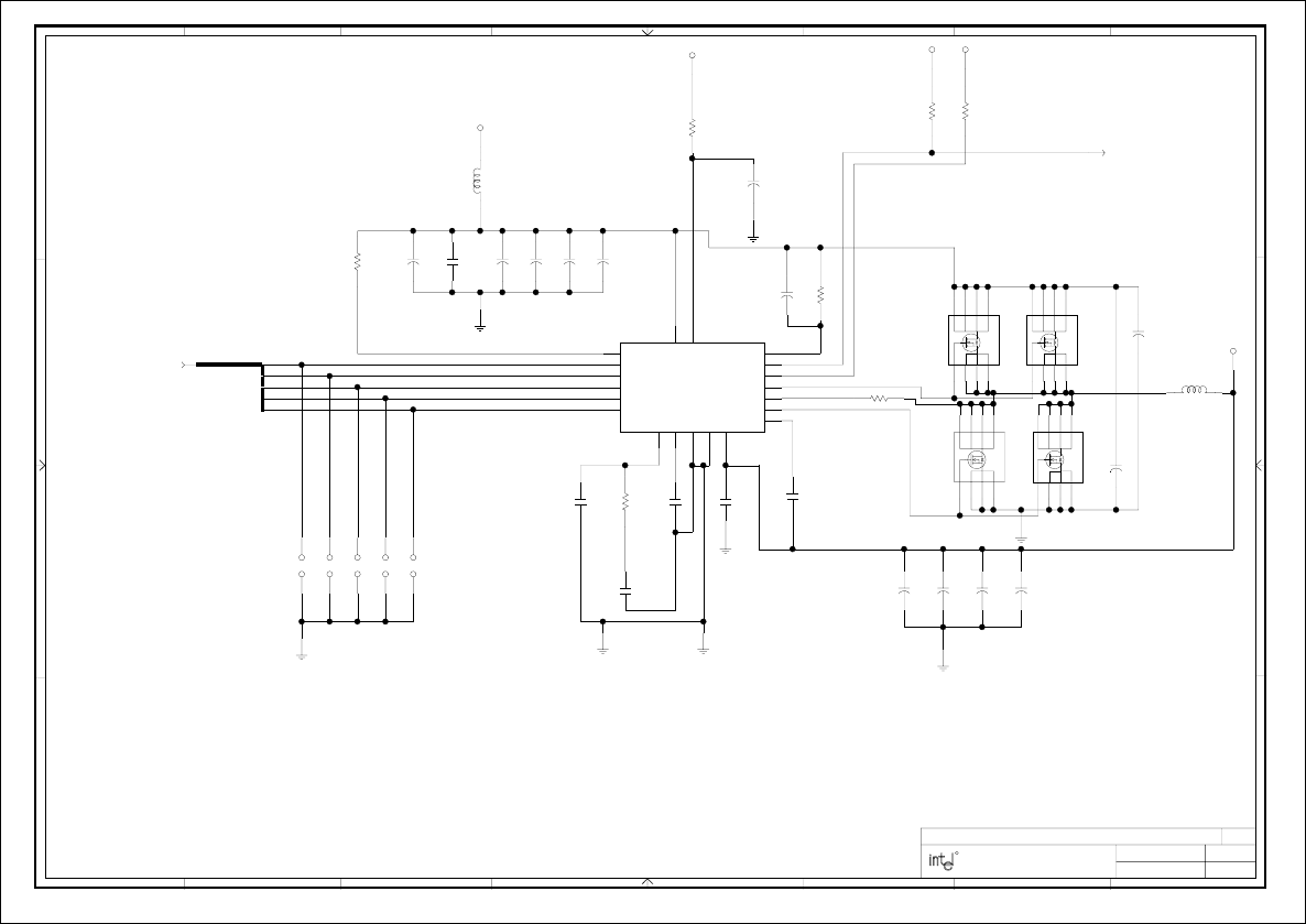
11-18-1999_11:24 28
VRM 8.2
VRM_G2
VRM_G1
Q4
4123
8765
R71
5.1-5%
OUTEN
VRM_PWRGD 4,31
2200UF
C100
2
1
C93
2200UF
1
2
2200UF
C103
2
1
JP9JP10 JP7JP6 JP8
R65
20
1200UF
C87
2
1
C111
1200UF
1
2
1200UF
C107
2
1
R55
8.2K
R53
5.6K
R332
220
3VID[4:0]
VID2
VID3
VID4
VID0
VID1
2.7K
R54
VRM_COMP
VRM_SS
VRM_IFB
VRM_FAULT
VRM_VFB
VRM_COMP_R
R80
10K
C82
1200UF
1
2
C110
2200UF
1
2
Q5
5678
3214
Q3
5678
3214
Q2
4123
8765
PVCC_R
C72
0.01UF
1
2
C90
0.1UF
C73
150PF
C75
0.1UF
C86
0.1UF
10UF
C140
2
1
C74
0.01UF
C71
1000PF
1UF-X7R
C118
2
1
1UF-X7R
C119
1
2
VR3
18
17
16
15
14
19
6
9
4
3
7
13
20
8
1
5
2
12
10
11
VRM_IMAX
ETQP6F0R8L
1.0UH-20A
L18
IFB_Q
VRM_VCC5
DO3316P-102
1UH
L19
1UF-X7R
C97
2
1
PCD PLATFORM DESIGN
REV:
DRAWN BY:
LAST REVISED:
PROJECT:
SHEET:
FOLSOM, CALIFORNIA 95630
1900 PRAIRIE CITY ROAD
87654321
A
B
C
D
12345678
D
C
B
A
1.01
TITLE: INTEL(R) 820 CHIPSET CUSTOMER REFERENCE BOARD
OF 36
R
G1
S1
S2
S3
D1
D2
D3
D4
SI4410DY
VCC3_3
+
+
+
+
+
+
VCCVID
VCC5
VCC12
+
+
G1
S1
S2
S3
D1
D2
D3
D4
SI4410DY
G1
S1
S2
S3
D1
D2
D3
D4
SI4410DY
G1
S1
S2
S3
D1
D2
D3
D4
SI4410DY
+
+
+
+
LTC1753
SENSE
SS
SGND
GND
VCC
PVCC
COMP
VID4
VID3
VID2
VID1
VID0
OUTEN IMAX
PWRGD
FAULT#
G1
G2
IFB
VFB
VCC5
+
Sanyo 4SP2200M
No Stuff C106
VID Override Jumpers
C118, C119 must be next to FETs.
C82,C87,C107,C111 must support >6A of RMS current.
Place caps next to output FETs.
VRM
VRM requirements are based on VRM8.4 spec .
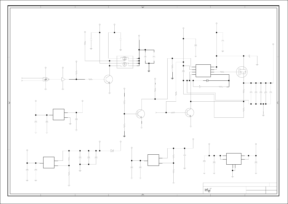
11-18-1999_11:24 29
VOLTAGE REGULATORS
100UF
C333
2
1
100UF
C108
1
2
100-1%
R133
100-1%
R134
301-1%
R311
131-1%
R309
5.1-5%
R135
R146
1.21K-1% 1%
R141
301
7,9,16,31 PWROK
R331
1K
9,31 SLP_S3#
VR8
3
2
1
U18
7
14 6
5
4
VR4
LT1587-1_5
3
2
1
VD_G2VD_G1 VD_G3
VCC1_8_ADJ
VCC2_5_ADJ
VDDQ_FB
VDDQ_COMP_R
7.5K-1%
R137
VDDQ_G VDDQ_G2
U14
12
7
14
C324
47UF
1UF-X7R
C104
1
2
1UF-X7R
C268
2
1
100UF
C124
2
1
100UF
C142
1
2
100UF
C319
1
2
C159
100UF
2
1
100UF
C167
1
2
1UF-X7R
C35
1
2
C161
1UF-X7R
1
2
C91
100UF
2
1
C193
10UF
1
2
C174
1UF
2
1
47UF
C173
2
1
1UF-X7R
C200
2
1
C225
1UF-X7R
2
1
1UF-X7R
C211
1
2
C179
1UF-X7R
2
1
VR5
3
2
1
C160
220UF
21
VDDQ_COMP
330UF-T510
C15
2
1
LT1575
VR6
4
3
2
1
5
6
7
8
10PF
C164
C168
0.001UF
21
22UF
C242
1
2
LT1529-3_3
VR1
6
24
51
3
1500UF
C352
2
1
1500UF
C336
1
2
R340
1K
C311
100UF
2
1
R330
1K
C347
47UF
VCC5DUAL_R
R158
2.2K
R360
10K
19 TYPEDET#
R361
1K
R362
1K
VR_SDB
R218
1K
VR_SHUTDOWN
R363
0K
CR11
BAT17
AC
Q6
1
2
3
Q7
MMBT3904LT1
E
C
B
Q16
MMBT3904LT1
B
C
E
MMBT3904LT1
Q13
E
C
B
SI4562DY
Q12
8
5
2
4
1
3
7
6
PCD PLATFORM DESIGN
REV:
DRAWN BY:
LAST REVISED:
PROJECT:
SHEET:
FOLSOM, CALIFORNIA 95630
1900 PRAIRIE CITY ROAD
87654321
A
B
C
D
12345678
D
C
B
A
1.01
TITLE: INTEL(R) 820 CHIPSET CUSTOMER REFERENCE BOARD
OF 36
R
VCC3_3
VCC2_5SBY
+
+
VCC3_3SBY
VCC5
VCC2_5
VCC5DUAL
VCC5
VTT1_5
VCC3_3
VCC3_3SBY
VCC3_3
VCC5DUAL
VCC12
VCC12
VCC5SBY
VIN
VOUT
ADJ
LT1587ADJ
74LS132 VCC
GND
VCC5SBY
VIN
VOUT
GND
SN74LVC07A GND
VCC
VDDQ
+ +
+
+
+
+
+
+
+
+
+
+
+
+
+
+
+
VIN
VOUT
ADJ
LT1587ADJ
+
+
IPOS
INEG
GATE
COMP
SHDN
VIN
GND
FB
+
+
VIN VOUT
SHDN#
GND3
TAB
SENSE
+
+
+
VCC5SBY
VCC3_3
VCC1_8
VCC1_8
-
+
IRL2203NS
1
3
2
13
2
13
2
13
2
D1
D2A
G1
G2
S1
S2
D1A
D2
It should be used only for further regulation of lower voltage power planes
The VCC5DUAL plane should not drive any logic components requiring 5V.
because the true voltage of VCC5DUAL will not remain constant
Rdson of the FET is not negligible for large currents
VTT 1.5 VOLTAGE REGULATOR
VCC3_3SBY VOLTAGE REGULATOR
AGP VDDQ VOLTAGE REGULATOR
VCC 5V DUAL VOLTAGE SWITCHER
VCC2_5 VOLTAGE REGULATOR
VCC 1.8 VOLTAGE REGULATOR
Route VR6 GND to VDDQ output caps and then via to ground.
Voltage Regulators
Place C311 at regulator.
Place C108 and C333 at RIMM termination
SN74LVC07A has 5V input and output tolerance.
No stuff R363
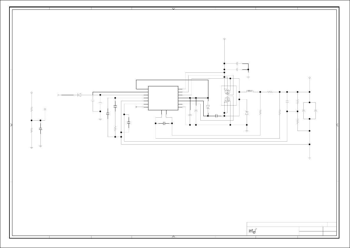
11-18-1999_11:28 30
VOLTAGE REGULATORS
SLP_S5#9
VCC2_5SBY_INTVCC
100-1%
R297
10K
R294
0.01
R325
R302
11K
100-1%
R258
35.7-1%
R259
CMDSH-3
CR9
C
A
VCC2_5SBY_ITH
VCC2_5SBY_VOSENSE
VCC2_5SBY_SENSE-
VCC2_5SBY_SENSE+
VCC2_5SBY_L
VCC2_5SBY_TG
VCC2_5SBY_BG
R295
10K
SBY_ITH_R
C295
68PF
1UF-X7R
C315
12
100-1%
R301
100PF
C304
100UF
C314 21
C312 0.1UF
V_BOOST
C306 4.7UF
1
2
C299 1000PF
C292
100PF
100PF
C293
C263
0.1UF
C307 0.1UF
2
1
330PF
C296
VR7
8
7
6
10
11
15
12
14
16
13
5
3
2
1
4
9
VCC2_5SBY_COSC
VCC2_5SBY_RUN
C294
0.1UF
CR8
MMBD914LT1
31
VCC2_5SBY_SW
CDRH127-6R1
10UH
L23
C326
330UF
2
1
C325
330UF
1
2
CR10
MBRS130LT3
C
A
SI4966DY
Q11
31
57
42
68
PCD PLATFORM DESIGN
REV:
DRAWN BY:
LAST REVISED:
PROJECT:
SHEET:
FOLSOM, CALIFORNIA 95630
1900 PRAIRIE CITY ROAD
87654321
A
B
C
D
12345678
D
C
B
A
1.01
TITLE: INTEL(R) 820 CHIPSET CUSTOMER REFERENCE BOARD
OF 36
R
VCC5DUAL
VCC2_5SBY
VCC2_5SBY
-
+
+
+
+
+
LT1435
RUN/SS
ITH
SGND
VIN
TG
SW
INTVCC
BOOST
BG
PGND
SENSE-
SENSE+
COSC
SFB
VOSENSE
EXTVCC
VCMOS1_8SBY
+
+
-
+
D1 D3
G1 G2
D2 D4
S1 S2
VCC 2.5 Standby Voltage Regulator
VCMOS Generator For Rambus
Do not stuff C292.
Do not stuff C304.
Voltage Regulators
T510
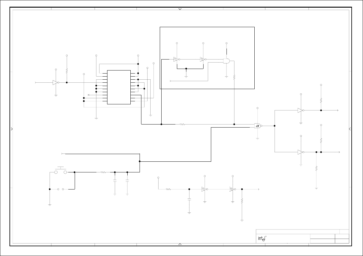
11-18-1999_11:28
POWER CONNECTOR
31
RSTBTN_SW
U20
7
14
3 4 7,9,16,29PWROK
0K
R339
4.7K
R349
R342
0K
1M
R288
R251
22K
9,29 SLP_S3#
R347
4.7K
SLP_S3
R343
22
U18
7
14 8
10
9
PWRGOOD 4
330
R96
1M
R348
J24
11
12
13
14
15
16
17
18
19
20
1
2
3
4
5
6
7
8
9
10
ATX_PWOK
POK_U1 POK_U2 POK_U3
RSMRST# 9,17
RSMRSTRSMRST_U
ATX_PWOK_R
PWROK_INV
U3
2
13
7
14
U15
34
7
14
U20 21 14
7
U15 14
7
65 U15
98
7
14
U20 65 14
7
4,28 VRM_PWRGD
4DBRESET#
10UF
C328C335
0.01UF
1UF
C266
U15 14
7
21
SW2
JP12
PCD PLATFORM DESIGN
REV:
DRAWN BY:
LAST REVISED:
PROJECT:
SHEET:
FOLSOM, CALIFORNIA 95630
1900 PRAIRIE CITY ROAD
87654321
A
B
C
D
12345678
D
C
B
A
1.01
TITLE: INTEL(R) 820 CHIPSET CUSTOMER REFERENCE BOARD
OF 36
R
VCC3_3SBY
VCC3_3SBY
VCC3_3SBY
SN74LVC06A GND
VCC
VCC3_3SBY
VCC3_3SBY VCC3_3SBY VCC3_3SBY
VCC12-
VCC12
VCC5
VCC5SBY
VCC3_3
VCC5SBY
74LS132 VCC
GND
VCC2_5
VCC5SBY
ATX
3_3V11
-12V
GND13
PS_0N
GND15
GND16
GND17
-5V
5V19
5V20
3_3V1
3_3V2
GND3
5V4
GND5
5V6
GND7
PW_OK
5VSB
12V
VCC3_3SBY
SN74LVC08A
74LVC14A
SN74LVC06A GND
VCC
VCC3_3SBY
74LVC14A 74LVC14A
VCC3_3SBY
SN74LVC06A GND
VCC
74LVC14A
330 ohm pullup to VCC3_3 located on CPU sheet.
For test only
and Schmitt trigger logic.
using a 22 msec delay
Resume Reset circuitry
No stuff.
For test only
No stuff.
ATX Connector
Reset Button
74LVC14A has 5V input tolerance.
ITP Reset circuit. For debug only.
SN74LVC06A has 5V input tolerance.
SN74LVC06A has 5V output tolerance.
220 ohm pullup to VCC3_3 is located on VRM sheet.
No stuff R342 when ITP is used.
Power Connector
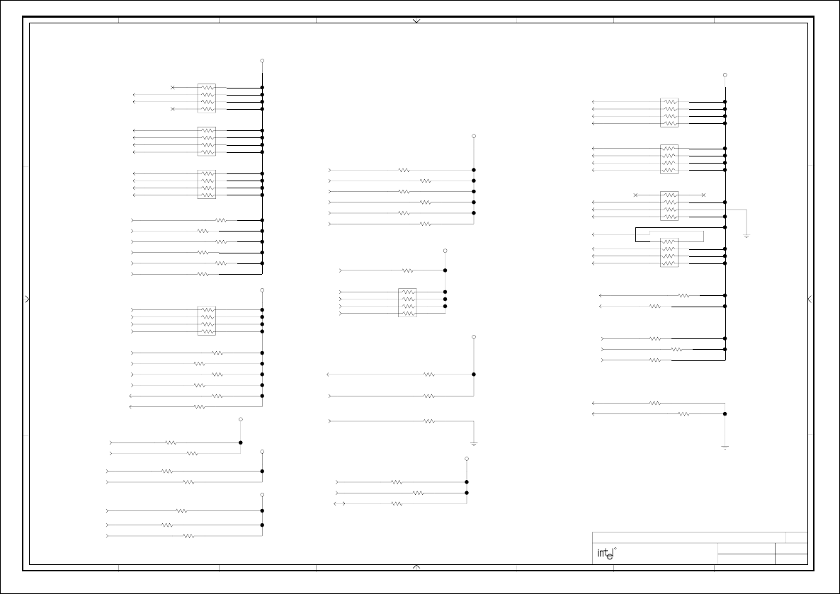
11-18-1999_11:29
PCI/AGP PULLUPS/PULLDOWNS
32
ST0
7,19
ST1
7,19
7,19 ST2 R507
8.2K
SBSTB#
7,19
7,19 SBSTB
7,19 GGNT#
WBF#
7,19
7,19 PIPE#
PIRQ#B
8,19,20,21
PIRQ#A
8,16,19,20,21
8.2K
R89
R81
8.2K
ALERTCLK_SBY
9,16 4.7K
R13
R12
4.7K
GNT#A
8,21
8,22 IRQ15
8,22 IRQ14
8.2K
R323
R338
8.2K
SMB_ALERT
94.7K
R236
R94
150
150
R85
SMBDATA_CORE
3,9,11
R237
4.7K
4.7K
R235
BREQ#0
4
R314
8.2K
4,8,10 HINIT#
4,8 LINT1
4,8 LINT0
4,8 A20M#
PREQ#3
8,16
PREQ#1
8,20
8,20 PREQ#0
8,12 A20GATE
8,12 KBRST#
8.2K
R198
8,16,20,21 PERR#
8,16,20,21 SERR#
8,16,20,21 STOP#
PGNT#4
8
PGNT#3
8,16 PGNT#2
8,21
PGNT#1
8,20
8,20 PGNT#0
19 GPERR#
19 GSERR#
7,19 GSTOP#
7,19 GFRAME#
R124
150
7,19 GIRDY#
8.2K
R327
R132
8.2K
ADSTB1
7,19
RBF#
7,19
7,19 GPAR
7,19 ADSTB#0
8.2K
R207
R136
8.2K
ADSTB#1
7,19
4,8 IGNNE#
PICD0
4,8
4,8 SMI#
4,8 STPCLK#
4FLUSH#
PICD1
4,8
R324
8.2K
SERIRQ
8,12,21
4TESTHI
SLP#
4,8
100K
R127
R102
10
R95
150
7,19 ADSTB0
REQ#A
8,21
ALERTDATA_SBY
9,16
150
R123
150
R126
7,19 GTRDY#
RP15
8.2K
1
2
3
45
6
7
8
7,19 GDEVSEL#
8.2K
RP9 1
2
3
45
6
7
8
RP14
8.2K
8
7
6
54
3
2
1
RP8
8.2K
1
2
3
45
6
7
8
8,16,20,21 TRDY#
8,16,20,21 FRAME#
8,16,20,21 IRDY#
RP10
2.7K
1
2
3
45
6
7
8
8,20,21 PLOCK#
8,20,21 PIRQ#C
8,20,21 PIRQ#D
RP11
2.7K
8
7
6
54
3
2
1150
R128
2.7K
R112
8,21 PGNT#5
8,21 PREQ#5
PREQ#2
8,21
R111
2.7K
2.7K
R115
R216
2.7K R213
2.7K
R109
2.7K
8PREQ#4
8.2K
RP16 1
2
3
45
6
7
8
8.2K
R214
R256
8.2K R114
8.2K
8.2K
R105
8,16,20,21 DEVSEL#
SMBCLK_CORE
3,9,11
RP6
2.7K
8
7
6
54
3
2
1
GREQ#
7,19
4,8 FERR#
R84
150
RP7
150
8
7
6
54
3
2
1
8.2K
R505
R506
8.2K
PCD PLATFORM DESIGN
REV:
DRAWN BY:
LAST REVISED:
PROJECT:
SHEET:
FOLSOM, CALIFORNIA 95630
1900 PRAIRIE CITY ROAD
87654321
A
B
C
D
12345678
D
C
B
A
1.01
TITLE: INTEL(R) 820 CHIPSET CUSTOMER REFERENCE BOARD
OF 36
R
VCC3_3
VCC5
VDDQ
VCC2_5
VCC2_5
VCC3_3
VCC2_5
VCC5
VCC3_3
VCC3_3SBY
AGP
PROCESSOR
PCI
PCI/AGP Pullups/Pulldowns
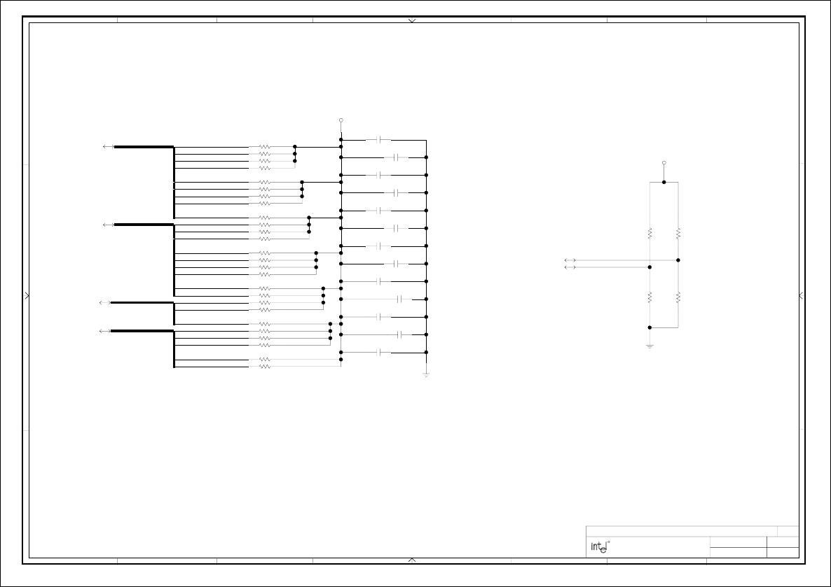
11-18-1999_14:01 33
RAMBUS TERMINATION
11
TERM_ROW[2:0]
TERM_ROW1
TERM_ROW0
TERM_ROW2
11
TERM_DQB[8:0] TERM_DQB0
TERM_DQB2
TERM_DQB3
TERM_DQB4
TERM_DQB5
TERM_DQB6
TERM_DQB7
TERM_DQB8
TERM_DQB1
11
TERM_COL[4:0]
TERM_COL3
TERM_COL2
TERM_COL0
TERM_COL1
TERM_COL4
11
TERM_DQA[8:0]
TERM_DQA8
TERM_DQA3
TERM_DQA2
TERM_DQA1
TERM_DQA6
TERM_DQA5
TERM_DQA4
TERM_DQA0
TERM_DQA7
11 TERM_SCK
TERM_CMD
11
C280
0.1UF C278
0.1UF
C281
0.1UF C282
0.1UF
0.1UF
C283
0.1UF
C273
0.1UF
C275
0.1UF
C274
0.1UF
C276
0.1UF
C279
0.1UF
C271
C269
0.1UF
C277
0.1UF
R277
28 R279
28 R278
28 R281
28
28 R280
28 R283
28 R282
28 R285
R284
28 R268
28 R267
28 R266
28
28 R265
28 R264
28 R263
28 R262
R261
28 R260
28 R275
28 R274
28
R276
28 R269
28
28 R271
28 R270
28 R273
28 R272
90.9-1% R293R292
39.2-1%
R290
39.2-1%
90.9-1% R291
PCD PLATFORM DESIGN
REV:
DRAWN BY:
LAST REVISED:
PROJECT:
SHEET:
FOLSOM, CALIFORNIA 95630
1900 PRAIRIE CITY ROAD
87654321
A
B
C
D
12345678
D
C
B
A
1.01
TITLE: INTEL(R) 820 CHIPSET CUSTOMER REFERENCE BOARD
OF 36
R
VCC1_8
VCC1_8
Rambus Termination
NOTE :
per two RSL signals.
Use one 0.1uF cap
Stuff C270,C272 with 0 ohm resistors.
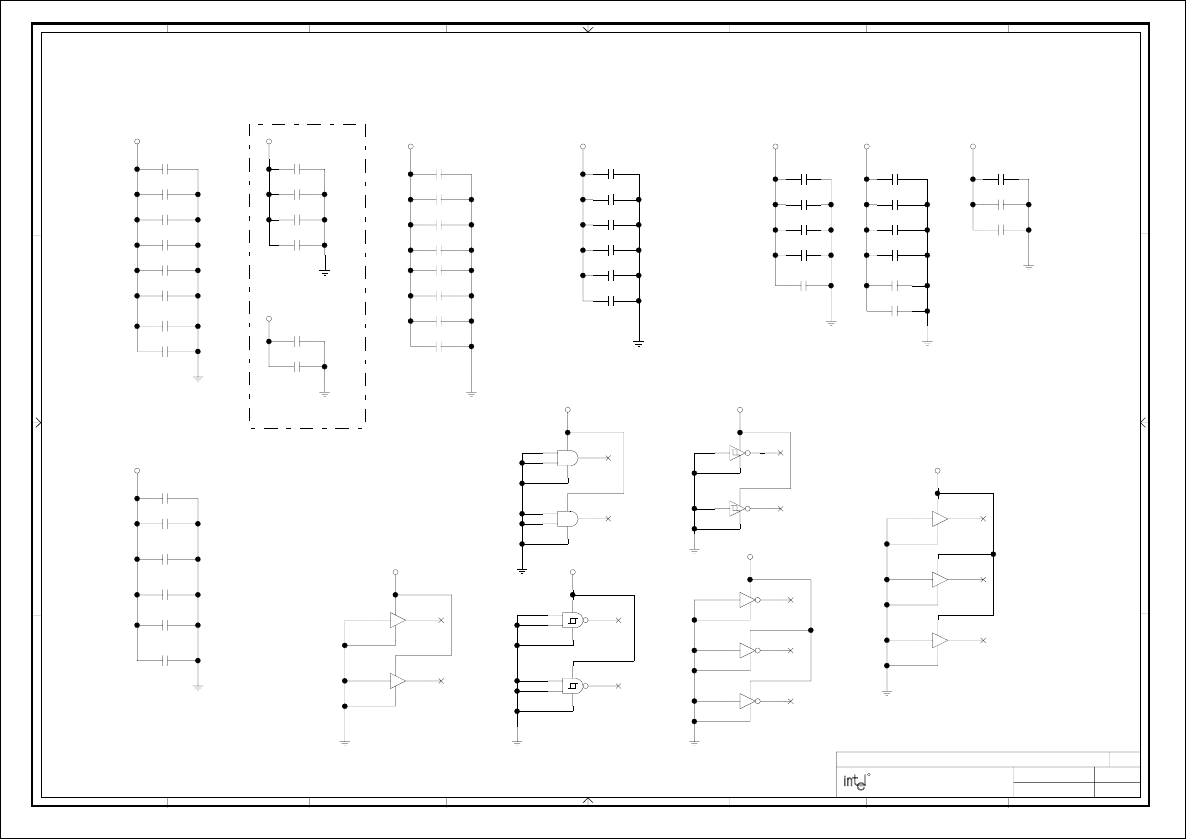
11-30-1999_10:26
DECOUPLING
34
C365
0.1UF
0.1UF
C366
0.1UF
C221
0.1UF
C60 C29
0.1UF
0.1UF
C30
C156
0.01UF
0.01UF
C213
0.1UF
C253
0.1UF
C231C232
0.1UF
C248
0.1UF
C254
0.01UF
0.01UF
C224C230
0.01UF
C252
0.01UF
0.1UF
C257C265
0.1UF
0.1UF
C184C260
0.1UF
C210
100UF
100UF
C285C219
100UF
C288
100UF
100UF
C284C289
100UF
100UF
C303
100UF
C302
C226
0.1UF
C105
0.1UF
4.7UF
C88C290
4.7UF
U3
10
98
7
14
U3
14
7
11
12
13
U15 14
7
1011
U15
13 12
7
14
U20 89 14
7
U20
7
14
11 10
U20 1213 14
7
U14
14
7
98
U18
12
13 11
14
7
U14
1011
7
14
U19
43
7
14
U19
14
7
11 10
U19
1213
7
14
U18
7
14 3
2
1
C202
0.01UF
C212
0.1UF
C157
0.1UF
0.1UF
C197
0.1UF
C235 C264
0.1UF
0.01UF
C162
C258
0.1UF
0.01UF
C368 C201
0.01UF
0.01UF
C367
0.01UF
C166 C343
0.01UF
0.01UF
C344
0.01UF
C261C262
0.01UF
PCD PLATFORM DESIGN
REV:
DRAWN BY:
LAST REVISED:
PROJECT:
SHEET:
FOLSOM, CALIFORNIA 95630
1900 PRAIRIE CITY ROAD
87654321
A
B
C
D
12345678
D
C
B
A
1.01
TITLE: INTEL(R) 820 CHIPSET CUSTOMER REFERENCE BOARD
OF 36
R
VCC5SBY
VCC3_3
VCMOS1_8SBYVCC2_5SBYVCC2_5SBY
SN74LVC08A
SN74LVC08A
74LVC14A
74LVC14A
VCC3_3SBY
SN74LVC06A GND
VCC
SN74LVC06A GND
VCC
SN74LVC06A GND
VCC
SN74LVC07A GND
VCC
74LS132 VCC
GND
VCC3_3SBY
SN74LVC07A GND
VCC
VCC3_3SBY
SN74LVC07A GND
VCC
SN74LVC07A GND
VCC
SN74LVC07A GND
VCC
74LS132 VCC
GND
VCC3_3SBY
VCC3_3 VCC3_3SBY
VCC1_8
VDDQ
VCC1_8
VDDQ
Place these caps on solder side
70 mils of outer balls of MCH.
Place VDDQ capacitors within
For chipset decoupling, use 0.1UF and
0.01UF decoupling capacitor at each
corner of the device. If there is room,
add 0.01UF capacitors in the middle
of each quad.
Place a VCMOS1_8SBY 0.1uF cap at each RIMM.
Un-used Gates
Place 100uF caps, 0.1 ohm ESR, among RIMM connectors.
RIMM Decoupling82559 Decoupling.ICH Decoupling
Decoupling
Place these caps on solder side
MCH Decoupling
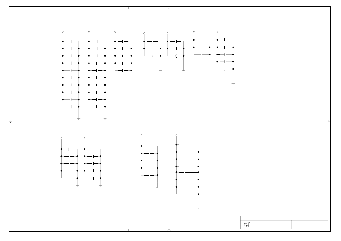
11-18-1999_11:31
BULK DECOUPLING
35
C89
0.1UF
C36
0.1UF
0.1UF
C216
0.1UF
C125C143
0.1UF
0.1UF
C153C154
0.1UF
0.1UF
C151C181
0.1UF
0.1UF
C238C188
0.1UF
C114
0.1UF
0.1UF
C310C351
0.1UF
0.1UF
C146C175
0.1UF
0.1UF
C145C177
0.1UF
0.1UF
C144C176
0.1UF
0.1UF
C178
0.1UF
C147
0.1UF
C172C195
0.1UF
0.1UF
C106C152
0.1UF
0.1UF
C163
C357
0.1UF
0.1UF
C65C259
0.1UF
0.1UF
C64
0.1UF
C240
0.1UF
C330C337
0.1UF
C332
0.1UF
0.1UF
C341
C345
0.1UF
C334
0.1UF 0.1UF
C331
22UF
C346 21
C338
22UF
12
22UF
C342 21
C127
0.1UF
C129
0.1UF
0.1UF
C150
0.1UF
C149
0.01UF
C128C130
0.01UF
0.01UF
C115
0.01UF
C148
10UF
C136C131
10UF
10UF
C139
10UF
C134
C141
10UF
10UF
C132C138
10UF
C133
10UF
C137
10UF 10UF
C135
22UF
C340 12
0.1UF
C339
PCD PLATFORM DESIGN
REV:
DRAWN BY:
LAST REVISED:
PROJECT:
SHEET:
FOLSOM, CALIFORNIA 95630
1900 PRAIRIE CITY ROAD
87654321
A
B
C
D
12345678
D
C
B
A
1.01
TITLE: INTEL(R) 820 CHIPSET CUSTOMER REFERENCE BOARD
OF 36
R
VCC3_3SBY
VCC2_5
VTT1_5
VCCVIDVCCVID
VCC12 VCC12-
VCC5
VCC3_3 VCC3_3
+
+ +
VCC3_3
+
Bulk Power Decoupling
Core Voltage Decoupling
VCC3_3 Decoupling VCC3_3 Decoupling VCC2_5 Decoupling
Decoupling
Termination Decoupling
Place caps at VTT pins on Slot 1 connector.

11-24-1999_11:38
REVISION HISTORY
36
PCD PLATFORM DESIGN
REV:
DRAWN BY:
LAST REVISED:
PROJECT:
SHEET:
FOLSOM, CALIFORNIA 95630
1900 PRAIRIE CITY ROAD
87654321
A
B
C
D
12345678
D
C
B
A
1.01
TITLE: INTEL(R) 820 CHIPSET CUSTOMER REFERENCE BOARD
OF 36
R
Changed VDDQ cap values from 0.1uF to 0.01uF.
Deleted 3.3V decoupling for RIMM connectors. Added solder side decoup for MCH.
Changed value of capacitor C194 from 0.1uF to 0.01uF.
and changed 39 ohm to 39.2 ohm resistors.
Revision 1.01
Revision History
Modified CMD and SCK termination values. Removed 470pF capacitors, Changed 93 ohm to 90.9 ohm,
Pg 6 Modified MCH_AGPREF circuit, changed 432 ohm to 1K ohm and 62 ohm to 80.6 ohm.
Pg 8
Pg 11
Modified HUBREF circuit, deleted R222, R223 & C217, changed C218 from 470pF to 0.1uF.
Modified RIMM connectors to eliminate 3.3V, added 0.1uF decoup caps to SVDDA & SVDDB on each RIMM.
Pg 33
Pg 34
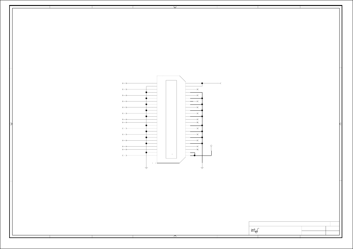
37
TEST_CLK66
5
HL7
7,8
HL6
7,8
HL5
7,8
HL4
7,8
HL8
7,8
HL10
7,8
HL_STB#
7,8
HL_STB
7,8
HL9
7,8
HL3
7,8
HL2
7,8
HL1
7,8
HL0
7,8
6,8HUBREF
J26
11
50 48 4218 16 14 12 10 8 646 44 42 40 38 36 34 32 30 28 26 24 22 20
17 15 13 97549 47 45 43 41 39 337 35 33 31 29 27 25 23 21 19 1
PCD PLATFORM DESIGN
REV:
DRAWN BY:
LAST REVISED:
PROJECT:
SHEET:
FOLSOM, CALIFORNIA 95630
1900 PRAIRIE CITY ROAD
87654321
A
B
C
D
12345678
D
C
B
A
1.01
TITLE: INTEL(R) 820 CHIPSET CUSTOMER REFERENCE BOARD
OF 36
R
VCC1_8
P08-050-SL-A-G
PROBE CONNECTOR
Hub Link Connector
For debug only.

B
Reference Board
Schematics: Dual-Processor
This page is intentionally left blank.

Intel®820 Chipset Design Guide B-1
Reference Design Schematics: Dual-Processor
Reference Design Schematics:
Dual-Processor B
B.1 Reference Design Feature Set
The reference schematics feature the following core feature set:
•Intel® 820 Chipset
— Memory Controller Hub (MCH)
— I/O Controller Hub (ICH)
— FWH Flash BIOS interface
•Support for the two Pentium III (SC242) Processors
— 100/133 MHz System Bus Frequency
— Debug Port
•IOAPIC Integrated into the ICH
•Direct RDRAM Memory Interface
— 266 MHz, 300 MHz, 356 MHz and 400 MHz Direct RDRAM Support
— 2 RIMM Sockets
•4 PCI Add-in Slots
— Via 4 REQ/GNT pairs (ICH supports 6 REQ#/GNT# pairs)
•AGP Universal Connector
— 3.3V - 1X,2X signaling
— 1.5V – 1X, 2X, 4X signaling
•2 IDE Connectors with Ultra ATA/66 Support
•2 USB Connectors
•ATX Power Connector
•LPC Ultra I/O
— Floppy Disk Controller
— 1 Parallel Port, 2 Serial Ports
— Keyboard Controller
•AC‘97 Bus Connector and Audio Codec
•WfM Support
•Integrated System Management
•Integrated Power Management
— ACPI Rev. 1.0 Compliant
— APM Rev. 1.2 Compliant
•Pentium III on-board VRM 8.4 compliant regulator
•4 Layer Design

11-29-1999_14:43 1
INTEL(R) 820 CHIPSET
DUAL PROCESSOR CUSTOMER REFERENCE SCHEMATICS
PCD PLATFORM DESIGN
REV:
DRAWN BY:
LAST REVISED:
PROJECT:
SHEET:
FOLSOM, CALIFORNIA 95630
1900 PRAIRIE CITY ROAD
87654321
A
B
C
D
12345678
D
C
B
A
TITLE: INTEL(R) 820 CHIPSET DUAL PROCESSOR CUSTOMER REFERENCE BOARD 3.03
OF 38
R
Note that these schematics are preliminary and are subject to change.
THESE SCHEMATICS ARE PROVIDED “AS IS” WITH NO WARRANTIES WHATSOEVER,
INCLUDING ANY WARRANTY OF MERCHANTABILITY, FITNESS FOR ANY PARTICULAR
PURPOSE, OR ANY WARRANTY OTHERWISE ARISING OUT OF PROPOSAL,
SPECIFICATION OR SAMPLES.
Information in this document is provided in connection with Intel products. No license, express or
implied, by estoppel or otherwise, to any intellectual property rights is granted by this document.
Except as provided in Intel's Terms and Conditions of Sale for such products, Intel assumes no
liability whatsoever, and Intel disclaims any express or implied warranty, relating to sale and/or
use of Intel products including liability or warranties relating to fitness for a particular purpose,
merchantability, or infringement of any patent, copyright or other intellectual property right. Intel
products are not intended for use in medical, life saving, or life sustaining applications. Intel may
make changes to specifications and product descriptions at any time, without notice.
The Intel® 820 chipset may contain design defects or errors known as errata which may cause
the product to deviate from published specifications. Current characterized errata are available on
request.
Intel may make changes to specifications and product descriptions at any time, without notice.
Copyright © Intel Corporation 1999.
*Third-party brands and names are the property of their respective owners.
Title Page
Cover Sheet 1
Block Diagram 2
Processor Connector 3, 4, 5, 6
Clock Synthesizer 7
MCH 8, 9
ICH 10, 11
FWH 12
RIMM Sockets 13
Super I/O 14
Audio 15, 16
Audio/Modem Riser 17
LAN 18, 19
System 20
AGP Connector 21
PCI Connectors 22, 23
IDE Connectors 24
USB Connectors 25
Parallel Port 26
Serial Ports 27
Keyboard/Mouse/Floppy Ports 28
Game Port 29
VRM 30
Voltage Regulators 31, 32
Pow er Connector 33
PCI/AGP Pullups/Pulldow ns 34
Rambus Termination 35
Decoupling 36, 37
Revision History 38
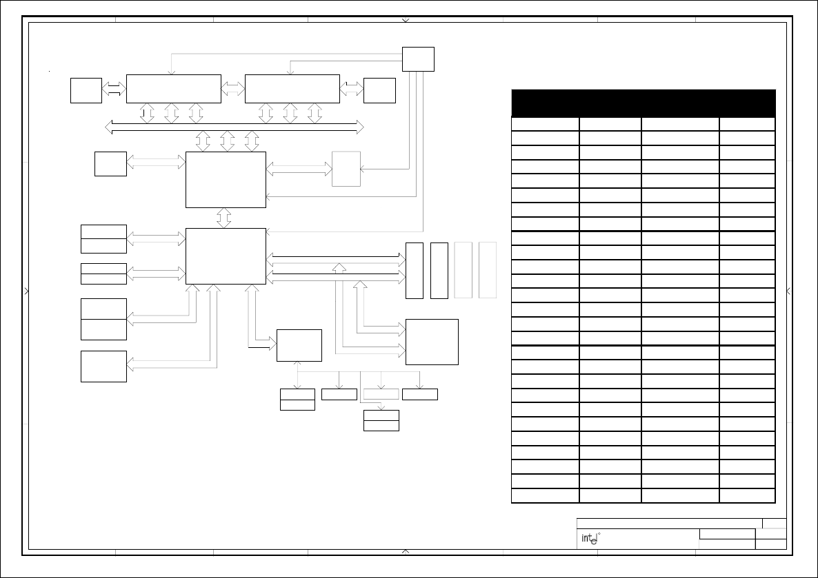
11-29-1999_14:43
BLOCK DIAGRAM
2
PCD PLATFORM DESIGN
REV:
DRAWN BY:
LAST REVISED:
PROJECT:
SHEET:
FOLSOM, CALIFORNIA 95630
1900 PRAIRIE CITY ROAD
87654321
A
B
C
D
12345678
D
C
B
A
TITLE: INTEL(R) 820 CHIPSET DUAL PROCESSOR CUSTOMER REFERENCE BOARD 3.03
OF 38
R
DATA
CTRL
ADDR
LPC Bus
Rambus
DATA
CTRL
ADDR
ADDR
CTRL
DATA
AGP Bus
PCI CONN 3
PCI CONN 1
PCI CONN 2
PCI CONN 4
PCI ADDR/DATA
PCI CNTRL
AC’97 Link
Clock
VRM
AGP
MCH
USB
ICH
IDE Primary
IDE Secondary
USB Port 1
USB Port 2
AC’97 Audio
Modem
SIO
Parallel Game ConnFloppyKeyboard
Mouse
Serial 1
Serial 2
82559 LAN
UltraDMA/66
FWH
Device Table
Block Diagram
Processor Processor
3 RIMM
Modules
VRM REFERENCE DEVICE GATES SHEET
DESIGNATOR TYPE USED NUMBER
U20 74LVC06A A, B, C, D, E, F 33, 36
U14 74LVC07A A, B, C, D, E, F 9,20,31,36
U19 74LVC07A A, B, C, D, E, F 20,24,36
U3 74LVC08A A, B, C, D 36, 33, 17
U9 74LVC08A A, B 33
U26 74LVC08A A 33
U15 74LVC14a A, B, C, D, E, F 33, 36
U23 74LVC14a A, B, C, D 33
U18 74LS132 A, B, C, D 31, 33, 36
U22 74LVC07A A, B 33
U25 74F74 A, B 4
U13 82801 (ICH) 10, 11
U10 82820 (MCH) 8, 9
U5 82559 18
U24 93C46A 18
U2 AD1881 15
U11 CK133 7
U12 DRCG 7
U16 FWH 12
U4, U6 GD75232 27
U1 LM4880 16
U17 LPC47B27X 14
U21 ADM1021 3
U8 ADM1021 5
U7 TPS2042 25
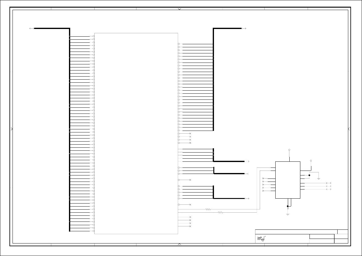
11-30-1999_9:55 3
PROCESSOR CONNECTOR
R100
R19
5,11,13,34SMBCLK_CORE
5,11,13,34SMBDATA_CORE
30
VID[4:0]
VID0
VID3
VID2
VID1
VID4
5,8
HA#[31:0]
HA#3
HA#4
HA#5
HA#6
HA#7
HA#8
HA#9
HA#11
HA#12
HA#13
HA#14
HA#15
HA#16
HA#17
HA#18
HA#19
HA#20
HA#21
HA#22
HA#23
HA#24
HA#25
HA#26
HA#27
HA#28
HA#30
HA#31
HA#29
HA#10
HREQ#[4:0] 5,8
HREQ#4
HREQ#0
HREQ#1
HREQ#2
HREQ#3
HD#0
HD#27
HD#28
HD#29
HD#30
HD#31
HD#32
HD#33
HD#34
HD#35
HD#36
HD#37
HD#38
HD#39
HD#40
HD#41
HD#42
HD#43
HD#44
HD#45
HD#46
HD#47
HD#48
HD#49
HD#50
HD#51
HD#52
HD#53
HD#54
HD#55
HD#56
HD#57
HD#58
HD#59
HD#60
HD#61
HD#62
HD#63
HD#26
HD#25
HD#24
HD#23
HD#22
HD#21
HD#20
HD#19
HD#18
HD#17
HD#16
HD#15
HD#14
HD#13
HD#12
HD#11
HD#10
HD#9
HD#8
HD#7
HD#6
HD#5
HD#4
HD#3
HD#2
HD#1
5,8
HD#[63:0]
5,8
RS#[2:0]
RS#2
RS#1
RS#0
5,11
THRM#
THRMDN_R
THRMDP_R
J15
A47
A88
A116
B119
A121
A119
A120
B120
B98
A100
A97
B78
A80
A79
B79
A83
A81
B80
B84
A84
B82
B88
B83
A87
A85
B87
B86
A89
A91
B91
A92
B90
A95
A93
B94
B92
A96
A99
B95
B96
B99
B114
B102
B103
A107
A108
B104
B115
B108
A112
B111
B32
B30
A32
A35
B38
B31
A37
B34
A33
B36
A36
B40
A41
B35
A40
B43
B39
A39
A44
A48
B44
A43
B42
B47
A45
B50
A49
B46
A52
B48
A51
B51
A53
A55
B54
B52
A56
B55
B56
A57
A59
A60
B58
B59
B62
B60
B63
A61
B64
A63
A67
B66
B72
A73
B71
A72
B70
A71
B68
B67
A69
A68
A65
A64
B12
B15
B14
THRMDN
THRMDP
ADM1021
U21
15
2
3
4
1
5
9
13
16
8
7
11
12
14
6
10
PCD PLATFORM DESIGN
REV:
DRAWN BY:
LAST REVISED:
PROJECT:
SHEET:
FOLSOM, CALIFORNIA 95630
1900 PRAIRIE CITY ROAD
87654321
A
B
C
D
12345678
D
C
B
A
TITLE: INTEL(R) 820 CHIPSET DUAL PROCESSOR CUSTOMER REFERENCE BOARD 3.03
OF 38
R
VCC3_3
0K
0K
RESERVED0
RESERVED1
RESERVED2
VID3
VID4
VID2
VID1
VID0
HA#3
HA#4
HA#5
HA#35
HA#34
HA#33
HA#32
HA#31
HA#30
HA#29
HA#28
HA#27
HA#26
HA#25
HA#24
HA#23
HA#22
HA#21
HA#20
HA#19
HA#18
HA#17
HA#16
HA#15
HA#14
HA#13
HA#12
HA#11
HA#10
HA#9
HA#8
HA#7
HA#6
RP#
REQ#0
REQ#1
REQ#2
REQ#3
REQ#4
RSP#
RS#0
RS#1
RS#2
HD#63
HD#62
HD#61
HD#60
HD#59
HD#58
HD#57
HD#56
HD#55
HD#54
HD#53
HD#52
HD#51
HD#50
HD#49
HD#47
HD#48
HD#46
HD#45
HD#43
HD#44
HD#42
HD#41
HD#40
HD#39
HD#38
HD#37
HD#36
HD#35
HD#34
HD#33
HD#32
HD#31
HD#30
HD#29
HD#28
HD#27
HD#26
HD#25
HD#24
HD#23
HD#21
HD#22
HD#19
HD#20
HD#18
HD#17
HD#16
HD#15
HD#13
HD#14
HD#12
HD#0
HD#1
HD#2
HD#3
HD#4
HD#5
HD#6
HD#7
HD#8
HD#9
HD#10
HD#11
RESERVED3
THRMDN
THRMDP
SC242
VCC3_3
ADD0
ADD1
SMBCLK
SMBDATA
ALERT#
GND7
GND8
NC16
NC13
NC9
NC5
NC1
DXN
DXP
VCC2
STBY#
THRMDP and THRMDN signals must be disconnected from onboard thermal sensor
during SECC2 thermal testing of the processor. Please see the "Pentium(R) II processor Single Edge
Contact Cartridge 2 Thermal Validation" document for further details.
Processor Connector 0
Place R19, R100 very close to processor.
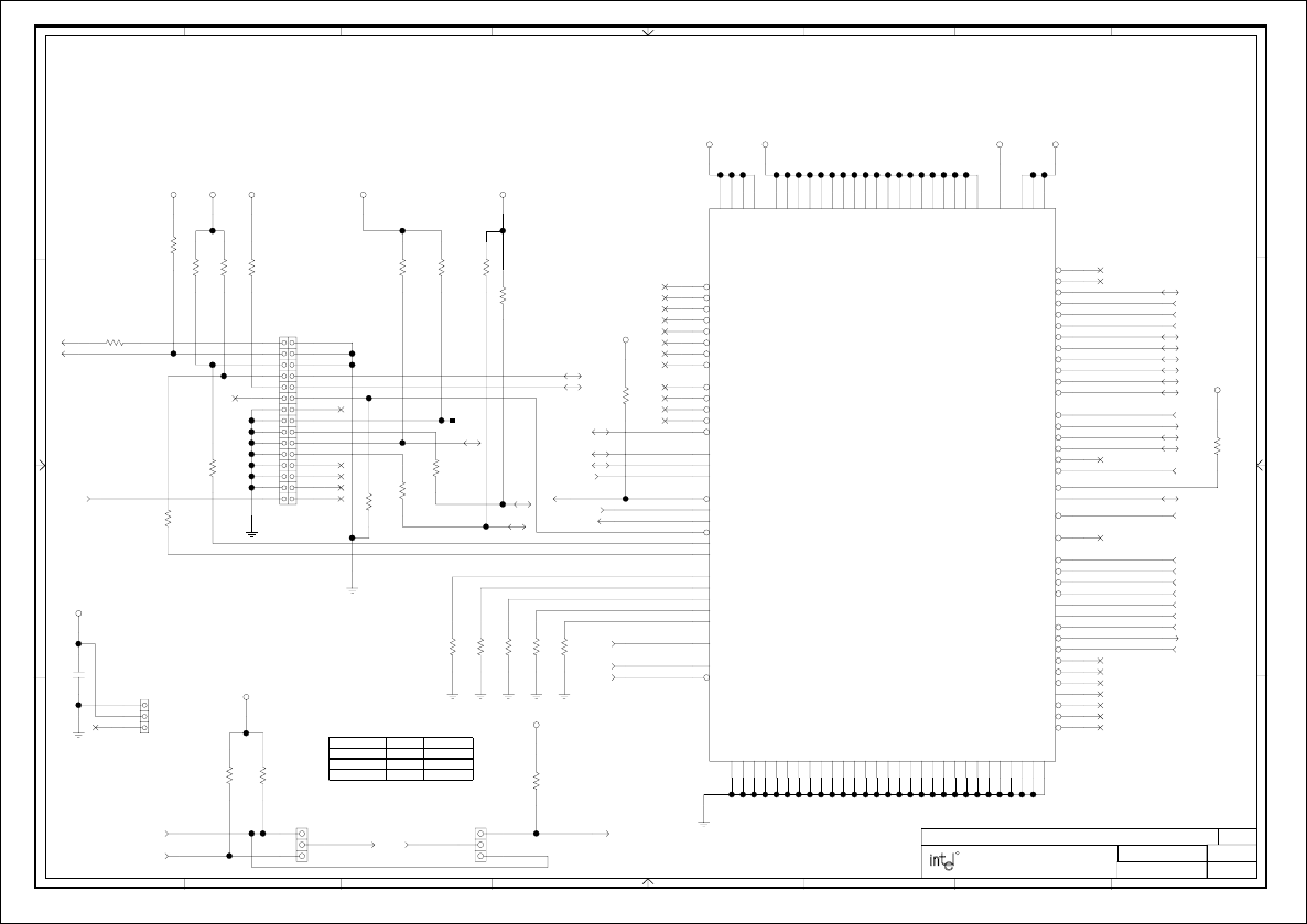
11-29-1999_14:45
PROCESSOR CONNECTOR
4
ITPPRDY# 4
150
R380
6BINIT#
6,10,34 PICD0
6,10,34 PICD1
7PICCLK
33 SLOTOCC0#
4 TDI_0
4,6 TDO_0
6,10,34
IGNNE# 6,10,34
FERR# 6,10,12,34
HINIT# 6,10,34
LINT1 6,10,34
LINT0 6,10,34
SMI# 6,10,34
SLP# 6,10,34
STPCLK# 6,10,34
A20M#
6,34
FLUSH#
6,7,9
SEL133/100#
34
TESTHI
6
BREQ#1 6
BREQ#0 4
ITPPRDY# 4
ITPREQ#
6,8
HADS# 6,8
DBSY# 6,8
HIT# 6,8
HITM# 6,8
DRDY# 6,8
HLOCK# 6,8
DEFER# 6,8
HTRDY#
6TCK
TMS
EMI1
EMI2
EMI3
EMI4
EMI5
6,7 CPUHCLK
6,33 PWRGOOD
4,6,8 CPURST#
6,8
BPRI# 6,8
BNR#
R92
150
JP34
1
2
3
JP33
3
2
1
6ITPREQ1#
330
R387
R386
240
ITPRDY#_R
6
TMS_R
ITPCLK
7
CPURST#_RCPURST#4,6,8
33 DBRESET#
XREF=6
TCK_R
ITP_PU_R
240
R95
47
R7
R11
47
680
R93
240
R159
R17
1K
R63
1K
1K
R18
J26
9
87
65
4
30
3
29
2827
2625
2423
2221
20
2
19
1817
1615
1413
1211
10
1
8.2K
R376
220
R375
0K
R1
0K
R2
0K
R3
0K
R4
0K
R5
0.1UF
C36
JP31
1
2
3
R94
240
ITPREQ# 4
330
R76
ITPRDY1#_R
R64
150
6 TDO_1
330
R388
4TDI_04,6 TDO_0
4 TDI4TDO
4TDI
4TDO
J15
B9
B5
A3
A1
B53
B49
B45
B37
B33
B29
B25
B17
B105
B97
B93
B89
B85
B77
B73
B69
B65
B57
B13
B109
B121
B117
B113
B11
A104
B10
A15
A13
A11
A9
B7
B6
B3
B8
B101
B74
B20
B112
A113
A16
A12
A20
B23
B22
A19
B18
B106
B16
A17
B4
A8
A4
A109
B110
A115
A38
A34
A30
A26
A22
A18
A14
A118
A114
A110
A106
A102
A98
A94
A90
A86
A82
A10
A78
A74
A70
A66
A62
A58
A54
A50
A46
A42
A6
A2
B76
B2
A7
B41
B1
B81
B100
B61
B107
B28
A31
A29
B27
A28
B26
A27
A25
A105
A111
A75
B75
A76
A103
B24
A23
A21
B19
A101
A24
A77
B116
A117
B118
A5
B21
6
ITPRDY1#
150
R218
6TRST#
PCD PLATFORM DESIGN
REV:
DRAWN BY:
LAST REVISED:
PROJECT:
SHEET:
FOLSOM, CALIFORNIA 95630
1900 PRAIRIE CITY ROAD
87654321
A
B
C
D
12345678
D
C
B
A
TITLE: INTEL(R) 820 CHIPSET DUAL PROCESSOR CUSTOMER REFERENCE BOARD 3.03
OF 38
R
VTT1_5
VCC3_3
VCC2_5
VCC3_3
VCC12
VCCVIDVTT1_5 VCC5 VCC3_3
VCC2_5
VCC2_5
VCC2_5VCC3_3
A20M#
AERR#
AP0#
AP1#
BERR#
BINIT#
BNR#
BP2#
BP3#
BPM0#
BPM1#
BPRI#
BREQ0#
BREQ1#
BCLK
DBSY#
DEFER#
DEP#0
DEP#1
DEP#2
DEP#3
DEP#4
DEP#5
DEP#6
DEP#7
DRDY#
EMI_1
EMI_2
EMI_3
EMI_4
EMI_5
FERR#
FLUSH#
RES4
GND0
GND1
GND10
GND11
GND12
GND13
GND14
GND15
GND16
GND17
GND18
GND19
GND2
GND20
GND21
GND22
GND23
GND24
GND25
GND26
GND27
GND28
GND29
GND4
GND5
GND6
GND7
GND8
GND9
HADS#
HIT#
HITM#
IERR#
IGNNE#
INIT#
LINT0
LINT1
LOCK#
PICCLK
PICD0
PICD1
PRDY#
PREQ#
PWRGOOD
RES0
RES3
RES2
RES1
RESET#
SLOTOCC#
SLP#
SMI#
STPCLK#
TCK
TDI
TDO
TESTHI
THMTRP#
TMS
TRDY#
TRST#
VCC3_1
VCC3_2
VCC3_3
VCC5
VCCP1
VCCP10
VCCP11
VCCP12
VCCP13
VCCP14
VCCP15
VCCP16
VCCP17
VCCP18
VCCP19
VCCP2
VCCP3
VCCP4
VCCP5
VCCP6
VCCP7
VCCP8
VCCP9
VTT1
VTT2
VTT3
VTT4
BSEL0
BSEL1
SC242
VTT1_5
R7 and R11 should be placed within 1" of ITP connector.
ITP
Processor Connector 0
CPU TACH0
ITP Config JP33 JP34
Single CPU0 1-2 1-2
Dual CPU 2-3 1-2
Single CPU1 2-3 2-3
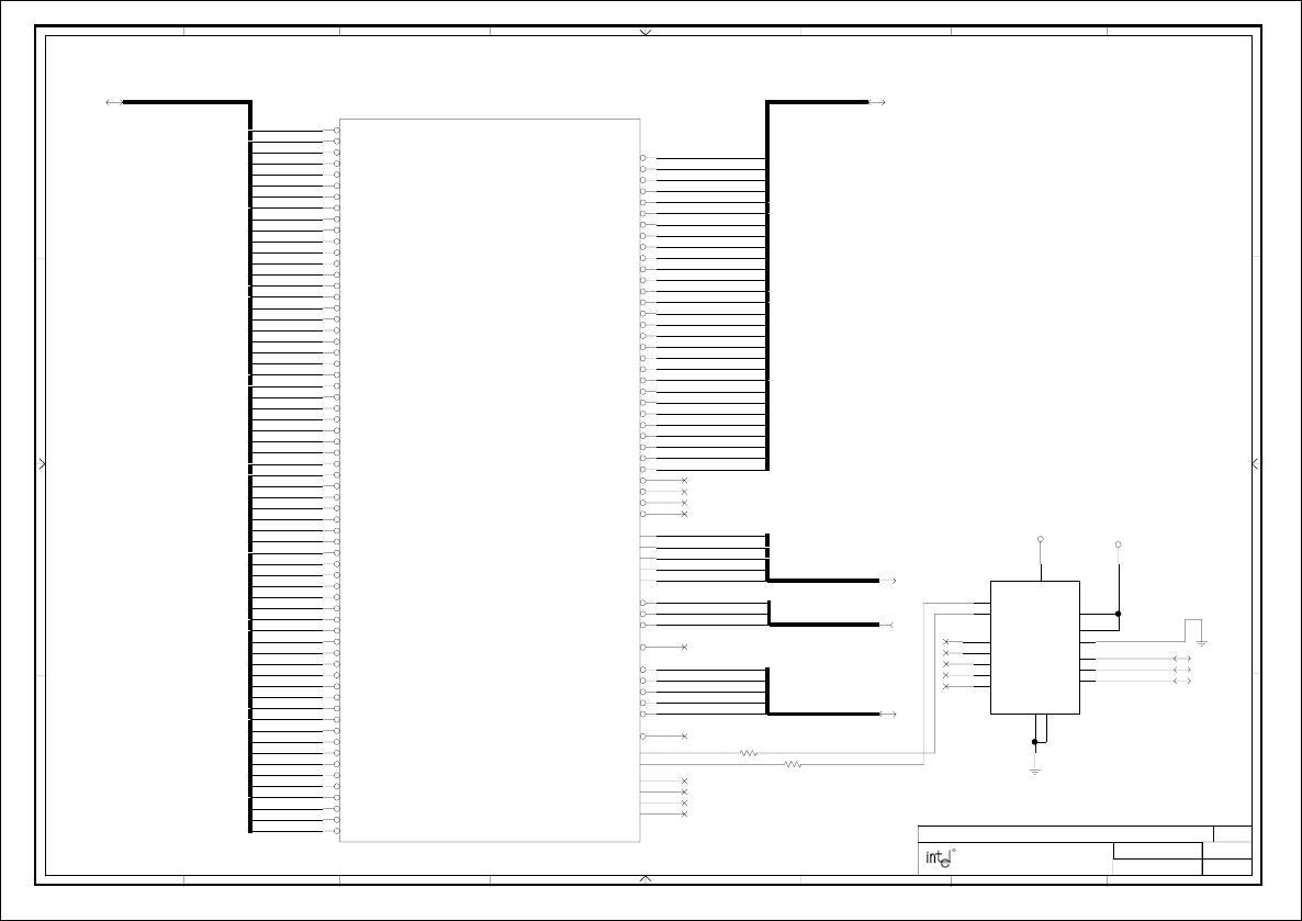
11-30-1999_9:57 5
PROCESSOR CONNECTOR
ADM1021
U8
15
2
3
4
1
5
9
13
16
8
7
11
12
14
6
10
R122
R121
3,11,13,34SMBCLK_CORE
3,11,13,34SMBDATA_CORE
30
VID1[4:0]
VID1[0]
VID1[3]
VID1[2]
VID1[1]
VID1[4]
3,8
HA#[31:0]
HA#3
HA#4
HA#5
HA#6
HA#7
HA#8
HA#9
HA#11
HA#12
HA#13
HA#14
HA#15
HA#16
HA#17
HA#18
HA#19
HA#20
HA#21
HA#22
HA#23
HA#24
HA#25
HA#26
HA#27
HA#28
HA#30
HA#31
HA#29
HA#10
HREQ#[4:0] 3,8
HREQ#4
HREQ#0
HREQ#1
HREQ#2
HREQ#3
HD#0
HD#27
HD#28
HD#29
HD#30
HD#31
HD#32
HD#33
HD#34
HD#35
HD#36
HD#37
HD#38
HD#39
HD#40
HD#41
HD#42
HD#43
HD#44
HD#45
HD#46
HD#47
HD#48
HD#49
HD#50
HD#51
HD#52
HD#53
HD#54
HD#55
HD#56
HD#57
HD#58
HD#59
HD#60
HD#61
HD#62
HD#63
HD#26
HD#25
HD#24
HD#23
HD#22
HD#21
HD#20
HD#19
HD#18
HD#17
HD#16
HD#15
HD#14
HD#13
HD#12
HD#11
HD#10
HD#9
HD#8
HD#7
HD#6
HD#5
HD#4
HD#3
HD#2
HD#1
3,8
HD#[63:0]
3,8
RS#[2:0]
RS#2
RS#1
RS#0
3,11
THRM#
THRMDN1_R
THRMDP1_R
THRMDN1
THRMDP1
J120
A47
A88
A116
B119
A121
A119
A120
B120
B98
A100
A97
B78
A80
A79
B79
A83
A81
B80
B84
A84
B82
B88
B83
A87
A85
B87
B86
A89
A91
B91
A92
B90
A95
A93
B94
B92
A96
A99
B95
B96
B99
B114
B102
B103
A107
A108
B104
B115
B108
A112
B111
B32
B30
A32
A35
B38
B31
A37
B34
A33
B36
A36
B40
A41
B35
A40
B43
B39
A39
A44
A48
B44
A43
B42
B47
A45
B50
A49
B46
A52
B48
A51
B51
A53
A55
B54
B52
A56
B55
B56
A57
A59
A60
B58
B59
B62
B60
B63
A61
B64
A63
A67
B66
B72
A73
B71
A72
B70
A71
B68
B67
A69
A68
A65
A64
B12
B15
B14
ADD0
ADD1
SMBCLK
SMBDATA
ALERT#
GND7
GND8
NC16
NC13
NC9
NC5
NC1
DXN
DXP
VCC2
STBY#
PCD PLATFORM DESIGN
REV:
DRAWN BY:
LAST REVISED:
PROJECT:
SHEET:
FOLSOM, CALIFORNIA 95630
1900 PRAIRIE CITY ROAD
87654321
A
B
C
D
12345678
D
C
B
A
TITLE: INTEL(R) 820 CHIPSET DUAL PROCESSOR CUSTOMER REFERENCE BOARD 3.03
OF 38
R
VCC3_3
0K
0K
VCC3_3
RESERVED0
RESERVED1
RESERVED2
VID3
VID4
VID2
VID1
VID0
HA#3
HA#4
HA#5
HA#35
HA#34
HA#33
HA#32
HA#31
HA#30
HA#29
HA#28
HA#27
HA#26
HA#25
HA#24
HA#23
HA#22
HA#21
HA#20
HA#19
HA#18
HA#17
HA#16
HA#15
HA#14
HA#13
HA#12
HA#11
HA#10
HA#9
HA#8
HA#7
HA#6
RP#
REQ#0
REQ#1
REQ#2
REQ#3
REQ#4
RSP#
RS#0
RS#1
RS#2
HD#63
HD#62
HD#61
HD#60
HD#59
HD#58
HD#57
HD#56
HD#55
HD#54
HD#53
HD#52
HD#51
HD#50
HD#49
HD#47
HD#48
HD#46
HD#45
HD#43
HD#44
HD#42
HD#41
HD#40
HD#39
HD#38
HD#37
HD#36
HD#35
HD#34
HD#33
HD#32
HD#31
HD#30
HD#29
HD#28
HD#27
HD#26
HD#25
HD#24
HD#23
HD#21
HD#22
HD#19
HD#20
HD#18
HD#17
HD#16
HD#15
HD#13
HD#14
HD#12
HD#0
HD#1
HD#2
HD#3
HD#4
HD#5
HD#6
HD#7
HD#8
HD#9
HD#10
HD#11
RESERVED3
THRMDN
THRMDP
SC242
THRMDP and THRMDN signals must be disconnected from onboard thermal sensor
during SECC2 thermal testing of the processor. Please see the "Pentium(R) II processor Single Edge
Contact Cartridge 2 Thermal Validation" document for further details.
Processor Connector 1
Place R121, R122 very close to processor.
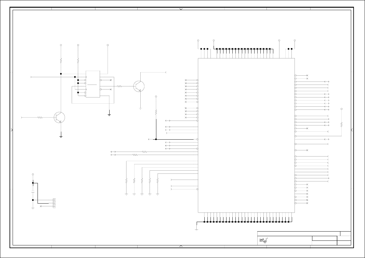
11-29-1999_14:45
PROCESSOR CONNECTOR
6
TCK_R4
2.7K
R102
BREQ#0 4,6
TCK
Q17
B
C
E
33 SLOTOCC1#
R389
220
4,7,9
SEL133/100#
EMI1_2
EMI1_3
EMI1_4
4,10,34
IGNNE# 4,10,34
FERR# 4,10,12,34
HINIT# 4,10,34
LINT1 4,10,34
LINT0 4,10,34
SMI# 4,10,34
SLP# 4,10,34
STPCLK# 4,10,34
A20M#
4,34
FLUSH#
4
ITPREQ1#
4,8
HADS# 4,8
DBSY# 4,8
HIT# 4,8
HITM# 4,8
DRDY# 4,8
HLOCK# 4,8
DEFER# 4,8
HTRDY#
EMI1_5
7CPUHCLK1
4,33 PWRGOOD
4,6,8 CPURST#
4,8
BPRI# 4,8
BNR#
7PICCLK1
EMI1_1
0K
R138
0K
R139
0K
R140
0K
R142
0K
R145
J120
B9
B5
A3
A1
B53
B49
B45
B37
B33
B29
B25
B17
B105
B97
B93
B89
B85
B77
B73
B69
B65
B57
B13
B109
B121
B117
B113
B11
A104
B10
A15
A13
A11
A9
B7
B6
B3
B8
B101
B74
B20
B112
A113
A16
A12
A20
B23
B22
A19
B18
B106
B16
A17
B4
A8
A4
A109
B110
A115
A38
A34
A30
A26
A22
A18
A14
A118
A114
A110
A106
A102
A98
A94
A90
A86
A82
A10
A78
A74
A70
A66
A62
A58
A54
A50
A46
A42
A6
A2
B76
B2
A7
B41
B1
B81
B100
B61
B107
B28
A31
A29
B27
A28
B26
A27
A25
A105
A111
A75
B75
A76
A103
B24
A23
A21
B19
A101
A24
A77
B116
A117
B118
A5
B21
0.1UF
C110
JP32
1
2
3
34
TESTHI1
PICD1
4,10,34
4TDO_0
TDO_1
4
TMS1
4,7 CPUHCLK
4,6,8 CPURST#
74F74
U25
8
6
10
13
4
1
5
9
11
12
14
3
2
7
4,6BREQ#0
4
ITPRDY1#
BREQ#1 4
4TRST#
2.7K
R101
4.7KR103 8.2K
R390
Q16
E
C
B
1K
R392
47
R391
TMS_R4
47
R395
PICD0
4,10,34
4BINIT#
PCD PLATFORM DESIGN
REV:
DRAWN BY:
LAST REVISED:
PROJECT:
SHEET:
FOLSOM, CALIFORNIA 95630
1900 PRAIRIE CITY ROAD
87654321
A
B
C
D
12345678
D
C
B
A
TITLE: INTEL(R) 820 CHIPSET DUAL PROCESSOR CUSTOMER REFERENCE BOARD 3.03
OF 38
R
VCC3_3
VCC5 VCC5
2N3904
13
2
VCC3_3
VCCVID1
VCC12
VTT1_5 VCC5 VCC3_3
A20M#
AERR#
AP0#
AP1#
BERR#
BINIT#
BNR#
BP2#
BP3#
BPM0#
BPM1#
BPRI#
BREQ0#
BREQ1#
BCLK
DBSY#
DEFER#
DEP#0
DEP#1
DEP#2
DEP#3
DEP#4
DEP#5
DEP#6
DEP#7
DRDY#
EMI_1
EMI_2
EMI_3
EMI_4
EMI_5
FERR#
FLUSH#
RES4
GND0
GND1
GND10
GND11
GND12
GND13
GND14
GND15
GND16
GND17
GND18
GND19
GND2
GND20
GND21
GND22
GND23
GND24
GND25
GND26
GND27
GND28
GND29
GND4
GND5
GND6
GND7
GND8
GND9
HADS#
HIT#
HITM#
IERR#
IGNNE#
INIT#
LINT0
LINT1
LOCK#
PICCLK
PICD0
PICD1
PRDY#
PREQ#
PWRGOOD
RES0
RES3
RES2
RES1
RESET#
SLOTOCC#
SLP#
SMI#
STPCLK#
TCK
TDI
TDO
TESTHI
THMTRP#
TMS
TRDY#
TRST#
VCC3_1
VCC3_2
VCC3_3
VCC5
VCCP1
VCCP10
VCCP11
VCCP12
VCCP13
VCCP14
VCCP15
VCCP16
VCCP17
VCCP18
VCCP19
VCCP2
VCCP3
VCCP4
VCCP5
VCCP6
VCCP7
VCCP8
VCCP9
VTT1
VTT2
VTT3
VTT4
BSEL0
BSEL1
SC242
VCC5
GND
D1
CLK1
VCC
D2
CLK2
Q2
Q1
CLR1#
PR1#
CLR2#
PR2#
Q1#
Q2#
2N3904
13
2
Processor Connector 1
CPU TACH1
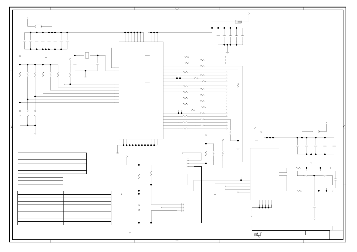
11-29-1999_14:46
CLOCK SYNTHESIZER
7
MULT1_GPIO11,14
4PF
C80
CK133_XIN
SIO_14MHZ_R
IHC_14MHZ_R
IHC_48MHZ_R
TEST_CLK66_R
ICH_CLK66_R
MCH_CLK66_R
SIO_PCLK7_R
FWHPCLK_R
PCLK5_R
PCLK4_R
PCLK3_R
PCLK2_R
PCLK1_R
ICHPCLK_R
ITPCLK_R
CPU_DIV2_2_R
CK133_XOUT
4,6,9 SEL133/100#
VCC_3_3_CK133_FB
PCISTOP#
CPUSTOP#
CK133_PWRDWN#
SPREAD#
SEL1
SEL0
VCC2_5_CK133_FB
PICCLK_R
33
R211
PCLK5 18
MULT1
R161
10K
10K
R206
10K
R203
JP15
9HCLKOUT
9RCLKOUT
22
PCLK1
14.318MHZ
Y3
21
22
R188
33
R165
33
R169
33
R186
33
R191
33
R183
23
PCLK3
23
PCLK4
12
FWHPCLK
11
ICH_14MHZ
R147 22
14
SIO_PCLK7
30
R166
AGPCLK_CONN 21
R195 33 9
MCH_CLK66
22
R221
R200
51-1%51-1%
R185
11
ICH_48MHZ
R217
10K
33
R194
JP14
10K
R202
11 MULT0_GPIO
JP17
R196
10K
R192
10K
22 R184
22 R189
33 R201
33
R187
FBHS01L
L20 21
L21
FBHS01L
12
FBHS01L
L22
12
22
R155
4
PICCLK
33
R220
11
ICH_CLK66
TEST_CLK66
R150
22
10
ICHPCLK
22
PCLK2
DRCG_CLK
DRCG_CLKB#
U12
21
17
2
12
11
24
23
22
20
18
16
15
14
10
7
6
9
8
5
4
3
1
13
R205
39-1%
R182
39-1%
VCC3_3_DRCG_FB
CLKTM_RD
0.1UF
C207
0.1UF
C215 C223
0.1UF
0.1UF
C186
0.1UF
C198
0.1UF
C206
0.1UF
C214
10PF
C185
10PF
C189
0.1UF
C199
0.1UF
C192
0.1UF
C190
0.1UF
C180
0.1UF
C208 C204
0.1UF
0.1UF
C220
10UF
C209
0.1UF
C196
10UF
C171
10UF
C170
0.1UF
C205
33
R210
14
SIO_14MHZ
R199
10K
R224
220
R197
10K
STOPB#
U11
5
55
30
29
28
27
26
25
24
23
22
21
20
19
18
17
16
15
14
13
12
11
10
9
8
7
6
4
3
2
1
31
32
33
34
35
36
37
38
39
40
41
42
43
44
45
46
47
48
49
50
51
52
53
54
56
10K
R219
10K
R204
MULT0
DRCG_PWRDWN#
R156
22
CPU_DIV2_1_R R148
22
4
ITPCLK
33
R164
CPU_DIV2
4,6
CPUHCLK
R170 22
8
MCHCLK
CPUHCLK1_R
CPUHCLK_R
6
CPUHCLK1
APICCLK_R
PICCLK1_R
APICCLK 10
PICCLK1 6
R151
22
CLKTM 13
13
CLKTM#
JP13
3
2
1
DRCG_CTRL11
JP11
JP18
1
2
3
PCD PLATFORM DESIGN
REV:
DRAWN BY:
LAST REVISED:
PROJECT:
SHEET:
FOLSOM, CALIFORNIA 95630
1900 PRAIRIE CITY ROAD
87654321
A
B
C
D
12345678
D
C
B
A
TITLE: INTEL(R) 820 CHIPSET DUAL PROCESSOR CUSTOMER REFERENCE BOARD 3.03
OF 38
R
VCC3_3
VCC3_3
XTAL
VCC3_3
VCC3_3
VCC2_5
VCC3_3
VCC2_5
DRCG
GND
VDDIR
VDDP
GNDP
GNDI
GNDC
VDDC
PCLKM
VDDIPD
MULT1
MULT0
VDDO1
CLKB#
CLK
VDDO2
S1
S0
STOPB#
PWRDN#
REFCLK
GNDO1
GNDO2
SYNCLKN
19 NC
VCC3_3
VCC1_8
VCC1_8
2_5V
CK133
VDD25V_1
APIC1
APIC0
VSS7
VDD25V_2
CPU_DIV2_1
CPU_DIV2_2
VSS8
VDD25V_3
CPUCLK3
CPUCLK2
VSS9
VDD25V_4
CPUCLK1
CPUCLK0
VSS10
VDD3V_6
VSS11
CPUSTOP#
PWRDWN#
SPREAD#
SEL1
SEL0
VDD3V_7
VSS1
REF0
REF1
VDD3V_1
XTAL_OUT
VSS2
PCICLK_F
PCICLK1
VDD3V_2
PCICLK2
PCICLK3
VSS3
PCICLK4
PCICLK5
VDD3V_3
PCICLK6
PCICLK7
VSS4
VSS5
3V66_0
3V66_1
VDD3V_4
VSS6
3V66_2
3V66_3
VDD3V_5
VSS12
48MHZ
APIC2
XTAL_IN
SEL133/100#
PCISTOP#
No stuff C80
No stuff R161, JP11.
CLKTM and CLKTM# RC network must use 5% or better tolerance components.
All jumpers may not be required, but are included for test purposes.
No stuff R106
for debug.
Provide at least one 0.1uF decoupling cap per power pin.
JP13 is for debug only.
VDDIR pin on DRCG should be decoupled at the component with a 0.1uF cap.
Tie CPUCLK and MCHCLK outputs together.
Clock Synthesizer
Keep stubs on unused outputs as short as possible.
HOST
BUS/RAMBUS JP13 JP18
100/300 2-3 OUT
100/400 OUT OUT
133/400 2-3 OUT
GPO CNTRL* 1-2 OUT
Sprd Spect JP14
Enabled* IN
Disabled OUT
SEL133/100# JP15 JP17 Function
0 IN IN All outputs Tri-State
0 IN OUT Reserved
0 OUT IN Active 100MHz, 48MHz PLL inactive
0 OUT OUT Active 100MHz, 48MHz PLL active
1 IN IN Test Mode
1 IN OUT Reserved
1 OUT IN Active 133MHz,48MHz PLL inactive
1 OUT OUT Active 133MHz,48MHz PLL active*
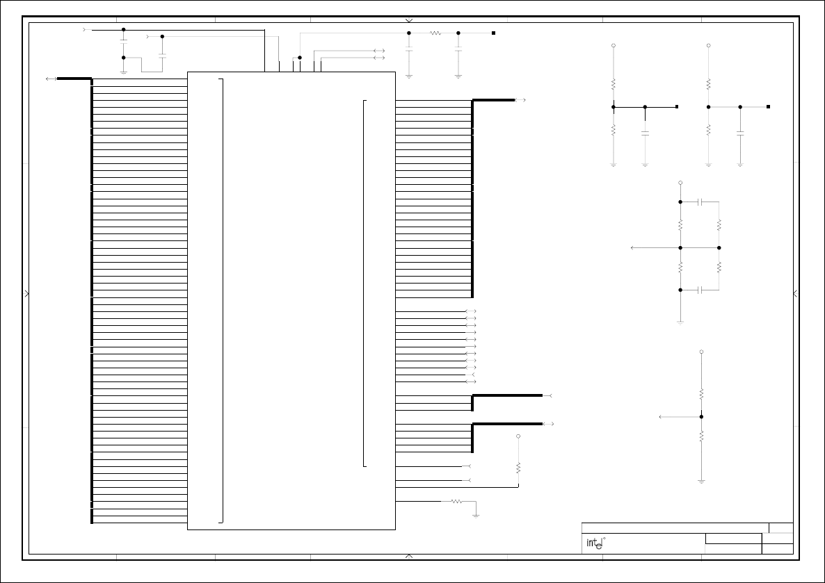
11-30-1999_10:02
MCH
8
HD#[63:0]
3,5 HD#0
HD#1
HD#2
HD#3
HD#4
HD#5
HD#6
HD#7
HD#8
HD#9
HD#10
HD#11
HD#12
HD#13
HD#14
HD#15
HD#16
HD#17
HD#18
HD#19
HD#20
HD#21
HD#22
HD#23
HD#24
HD#25
HD#26
HD#27
HD#28
HD#29
HD#30
HD#31
HD#32
HD#33
HD#34
HD#35
HD#36
HD#37
HD#38
HD#39
HD#40
HD#41
HD#42
HD#43
HD#44
HD#45
HD#46
HD#47
HD#48
HD#49
HD#50
HD#51
HD#52
HD#53
HD#54
HD#55
HD#56
HD#57
HD#58
HD#59
HD#60
HD#61
HD#63
HD#62
GRCOMP
MCH_HLCOMP
PCIRST# 10,12,13,14,18,21,22,23,24
MCHCLK 7
3,5
HREQ#[4:0]
HREQ#4
HREQ#3
HREQ#2
HREQ#1
HREQ#0
RS#[2:0]
3,5
RS#2
RS#1
RS#0
HTRDY# 4,6
HLOCK# 4,6
HITM# 4,6
HIT# 4,6
DRDY# 4,6
DEFER# 4,6
DBSY# 4,6
BPRI# 4,6
BNR# 4,6
HADS# 4,6
CPURST# 4,6
3,5
HA#[31:0]
HA#3
HA#4
HA#5
HA#6
HA#7
HA#30
HA#31
HA#29
HA#28
HA#27
HA#26
HA#25
HA#24
HA#23
HA#22
HA#21
HA#20
HA#19
HA#18
HA#17
HA#16
HA#15
HA#14
HA#13
HA#12
HA#11
HA#10
HA#9
HA#8
10 HUBREF
21 CONN_AGPREF RAMREF_R
8GTLREF2
8GTLREF1
MCH_AGPREF_CV
R143
75-1%
RAMREF 8,13
R190
162-1%
RAMREF
8,13
100-1%
R168
40.2-1%
R180
MCH_AGPREF_CG
40.2-1%
R129
R131
75-1%150-1%
R130
R144
150-1%
0.1UF
C155
0.1UF
C191
0.1UF
C203
C158
0.001UF
C182
470PF
562-1%
R181
0.001UF
C183
C187
470PF
U10
V2
Y1
W2
C3
V12
E11
E10
U14
E20
T15
A18
F20
G2
E3
E4
G4
H1
E2
C1
E5
F4
F3
E1
D3
F1
F2
D1
G1
F5
D2
P4
M5
N4
P3
P2
N1
P1
M4
N5
M1
M2
M3
N2
L2
K4
L4
K3
K5
J2
K1
J5
L1
J4
H2
H5
K2
G5
H4
H3
J1
W13
V14
Y14
U12
U11
W14
Y12
Y13
U13
T11
W12
V10
U10
T12
T10
Y11
T9
W11
Y9
U9
V8
Y10
W10
U8
W9
T7
W8
T8
Y7
Y8
U7
W7
T6
W6
V6
U6
W5
Y6
T5
V5
T4
Y5
Y4
T3
U4
V4
W3
W4
U2
U3
Y3
T2
U1
W1
Y2
V1
R5
T1
P5
R4
R1
R2
GTLREF2 GTLREF1
1K-1%
R154
1K-1%
R149
R153
80.6-1%
R160
80.6-1%
MCH_AGPREF
21
0.01UF
C194
PCD PLATFORM DESIGN
REV:
DRAWN BY:
LAST REVISED:
PROJECT:
SHEET:
FOLSOM, CALIFORNIA 95630
1900 PRAIRIE CITY ROAD
87654321
A
B
C
D
12345678
D
C
B
A
TITLE: INTEL(R) 820 CHIPSET DUAL PROCESSOR CUSTOMER REFERENCE BOARD 3.03
OF 38
R
VDDQ
VCC1_8
VTT1_5 VTT1_5
VCC1_8
VDDQ;F15,R15,J17,L17,N17,T17
MCH_096
GND;D9,J9,K9,L9,M9,V9,B10,J10,K10,L10,M10,C11,J11,K11,L11
GND;P19,T19,D20
GND;B15,D15,B16,D16,E16,F16,A17,E18,V18,A19,H19,K19,M19
HD#0
HD#1
HD#2
HD#3
HD#4
HD#5
HD#6
HD#7
HD#8
HD#9
HD#10
HD#11
HD#13
HD#15
HD#16
HD#17
HD#18
HD#19
HD#20
HD#21
HD#22
HD#23
HD#24
HD#25
HD#26
HD#27
HD#28
HD#29
HD#30
HD#31
HD#32
HD#33
HD#34
HD#35
HD#36
HD#37
HD#38
HD#39
HD#40
HD#41
HD#42
HD#43
HD#44
HD#45
HD#46
HD#47
HD#48
HD#49
HD#50
HD#51
HD#52
HD#53
HD#54
HD#55
HD#56
HD#57
HD#58
HD#59
HD#60
HD#61
HD#62
HD#63
HA#3
HA#4
HA#5
HA#6
HA#7
HA#8
HA#9
HA#10
HA#11
HA#12
HA#13
HA#14
HA#15
HA#16
HA#17
HA#18
HA#19
HA#20
HA#21
HA#22
HA#23
HA#24
HA#25
HA#26
HA#27
HA#28
HA#29
HA#30
HA#31
CPURST#
ADS#
BNR#
BPRI#
DBSY#
DEFER#
DRDY#
HIT#
HITM#
HLOCK#
HTRDY#
RS#0
RS#1
RS#2
HREQ#0
HREQ#1
HREQ#2
HREQ#3
HREQ#4
RSTIN#
HUBREF
AGPREF
RAMREFB
RAMREFA
GTLREFB
GTLREFA
HD#12
HD#14
HCLKIN
TEST/GRCOMP
HLCOMP
VCC1_8;D4,E6,F6,G6,E7,R6,R7,E8,E9,D10,D11,E12
VCC1_8;E13,E14,F14,T14,E15,P15,B17,C17,C19
GND;A1,A3,G3,J3,L3,N3,R3,V3,B4,D5,L5,U5,B6,D6,D7,V7,B8,D8
GND;M11,V11,C12,D12,J12,K12,L12,M12,B13,D13,V13,T13,D14
HOST HOST
Place R129 and R180 less than 0.5" from MCH using 10 mil trace.
Place MCH_AGPREF circuit near the MCH.
MCH
11-29-1999_14:46
MCH
9
C360
0.1UF
0.1UF
C359 C361
0.1UF
0.1UF
C362
4.7K
R248
PWROK11,18,31,33
U14
14
7
13 12
13LCMD
LSCK
13
SCK_CTRL
HL10
9,10
GAD1
GAD2
GAD3
GAD4
GAD5
GAD6
GAD7
GAD8
GAD9
GAD10
GAD11
GAD12
GAD13
GAD14
GAD15
GAD16
GAD17
GAD18
GAD19
GAD20
GAD21
GAD22
GAD23
GAD24
GAD25
GAD26
GAD27
GAD28
GAD29
GAD30
GAD31
21
GAD[31:0] GAD0
HL2
HL1
HL[10:0]
10
HL0
HL10
HL9
HL8
HL7
HL6
HL5
HL4
HL3
HL_STB 10
HL_STB# 10
13
LCLKFM# 13
LCLKFM 13
LCLKTM# 13
LCLKTM
LDQB0 13
LDQB[8:0]
LDQB1
LDQB2
LDQB3
LDQB4
LDQB5
LDQB6
LDQB7
LDQB8
LCOL0 13
LCOL[4:0]
LCOL1
LCOL2
LCOL3
LCOL4
13
LROW[2:0]
LROW0
LROW1
LROW2
LDQA6
LDQA7
LDQA8
LDQA4
LDQA3
LDQA2
LDQA1
LDQA0 13
LDQA[8:0]
LDQA5
GC/BE#2
GC/BE#1
GC/BE#0
GC/BE#[3:0]
21
GC/BE#3
21,34 GTRDY#
21,34 GIRDY#
21,34 GDEVSEL#
21,34 GFRAME#
GPAR
21,34
21,34 GSTOP#
SBSTB#
21,34
ADSTB1
21,34
ADSTB0
21,34
WBF#
21,34
21,34 PIPE#
21,34 GREQ#
21,34 GGNT#
ST2
ST0
ST1
ST[2:0]
21
7MCH_CLK66
21,34 RBF#
ADSTB#0
21,34
ADSTB#1
21,34 SBSTB
21,34
HCLKOUT 7
RCLKOUT 7
21
SBA[7:0]
SBA1
SBA3
SBA4
SBA5
SBA6
SBA7
SBA2
SBA0
LSIO 13
4,6,7
SEL133/100#
R209
8.2K
Q10
MMBT3904LT1
B
C
E
4.7K
R346
MMBT3904LT1
Q14
E
C
B
MMBT3904LT1
Q9
B
C
E
8.2K
R227
9
PWROK_CTRL
PWROK_CTRL9
U10
Y19
Y20
W17
Y18
W18
A16
A9
B9
C9
F19
C4
A4
B5
A5
C5
A6
C6
B7
C7
C16
A15
C15
B14
C14
A14
C13
A13
A2
B1
C20
D19
D18
C18
D17
A20
B18
B19
B20
E19
E17
F18
A7
C8
A8
A10
C10
B11
A11
A12
B12
B3
B2
C2
W20
V17
V20
W19
V19
U16
R19
R18
H20
J19
Y17
Y15
W15
V15
V16
W16
Y16
U15
K16
M18
M20
N20
N19
L16
R16
N18
L20
H16
U19
U20
T18
U18
T16
U17
R17
T20
R20
P16
P20
N16
P17
M16
P18
M17
L18
K20
L19
J18
K18
K17
J16
J20
H18
H17
G20
G16
G19
G17
G18
F17
PCD PLATFORM DESIGN
REV:
DRAWN BY:
LAST REVISED:
PROJECT:
SHEET:
FOLSOM, CALIFORNIA 95630
1900 PRAIRIE CITY ROAD
87654321
A
B
C
D
12345678
D
C
B
A
TITLE: INTEL(R) 820 CHIPSET DUAL PROCESSOR CUSTOMER REFERENCE BOARD 3.03
OF 38
R
VCC1_8
VCC3_3SBY
SN74LVC07A GND
VCC
VCC5SBY
1
3
2
13
2
13
2
VCC3_3SBY
MCH_096
HUB
AGP
MEMORY
AGP
G_AD0
G_AD1
G_AD2
G_AD3
G_AD4
G_AD5
G_AD6
G_AD7
G_AD8
G_AD9
G_AD10
G_AD11
G_AD12
G_AD13
G_AD14
G_AD15
G_AD16
G_AD17
G_AD18
G_AD19
G_AD20
G_AD21
G_AD22
G_AD23
G_AD24
G_AD25
G_AD26
G_AD27
G_AD28
G_AD29
G_AD30
G_AD31
G_C/BE#0
G_C/BE#1
G_C/BE#2
G_C/BE#3
G_FRAME#
G_DEVSEL#
G_IRDY#
G_TRDY#
G_STOP#
G_PAR
G_REQ#
G_GNT#
PIPE#
RBF#
WBF#
ST0
ST1
ST2
AD_STB0
AD_STB#0
AD_STB1
AD_STB#1
SBA7
SBA6
SBA5
SBA4
SBA1
SBA0
SIO
SCK
CMD
CFM#
CFM
CTM#
CTM
RQ7
RQ6
RQ2
RQ1
RQ0
HL1
HL2
HL3
HL4
HL5
HL6
HL7
HL8
HL9
HL10
HL_STB
HL_STB#
RCLKOUT
HCLKOUT
DQA0
DQA1
DQA2
DQA3
DQA4
DQA5
DQA6
DQA7
DQB0
DQB1
DQB2
DQB3
DQB4
DQB5
DQB6
DQB7
DQB8
HL0
RQ3
RQ4
RQ5
DQA8
CLK66
SBA2
SBA3
SB_STB
SB_STB#
LSCK and LCMD must neck down to 5 mils for 175 mils at Q10 and Q9 attach points.
Place Q10 and Q9 as close as possible to MCH.
MCH
No stuff. For test only.
11-29-1999_14:46 10
ICH
8,10 HUBREF
PGNT#5 23,34
PGNT#4 34
PGNT#3 18,34
23,34
PGNT#2
PGNT#1 22,34
PGNT#0 22,34
PREQ#5 23,34
PREQ#4 34
PREQ#3 18,34
PREQ#2 23,34
PREQ#1 22,34
22,34
PREQ#0
14,23,34
SERIRQ 4,6,34
PICD1
PICD0 4,6,34
7
APICCLK
IRQ15 24,34
IRQ14 24,34
22,23,34
PIRQ#D
PIRQ#C 22,23,34
21,22,23,34
PIRQ#B
PIRQ#A 18,21,22,23,34
8,10HUBREF
9
HL_STB#
9
HL[10:0]
HL10
HL9
HL8
HL7
HL6
HL5
HL4
HL3
HL2
HL1
HL0
AD[31:0]
18,22,23 AD0
AD1
AD2
AD3
AD4
AD5
AD6
AD7
AD8
AD9
AD10
AD11
AD12
AD13
AD14
AD15
AD16
AD17
AD18
AD19
AD20
AD21
AD22
AD23
AD24
AD25
AD26
AD27
AD28
AD29
AD30
AD31
18,22,23
C_BE#[3:0] C_BE#0
C_BE#1
C_BE#2
C_BE#3
DEVSEL#
18,22,23,34 FRAME#
18,22,23,34 IRDY#
18,22,23,34 TRDY#
18,22,23,34 STOP#
18,22,23,34 PAR
18,22,23 PCIRST#
8,12,13,14,18,21,22,23,24 PLOCK#
22,23,34 SERR#
18,22,23,34 PERR#
18,22,23,34
18,21,22,23 PCI_PME#
ICHPCLK
7
14,34
A20GATE 14,34
KBRST#
STPCLK# 4,6,34
4,6,34
SMI# 4,6,34
LINT1 4,6,34
LINT0
HINIT# 4,6,12,34
IGNNE# 4,6,34
4,6,34
FERR# 4,6,34
SLP#
A20M# 4,6,34
R226
301-1%
R225
301-1%
40.2-1%
R239
23,34 REQ#A
23,34 GNT#A
ICH_HLCOMP
HL11_TP
U13
M17
H17
G17
J17
H15
L17
K17
K16
G16
F17
D17
K1
E9
E2
E1
F5
F4
F3
F2
G4
G2
C13
A13
N6
D10
C14
R5
P5
J13
R4
C17
E16
F14
A15
B15
A17
B10
B7
E7
D8
C7
A12
C12
B13
D12
B11
B12
A14
F16
J14
B16
E14
B17
B9
A9
C4
D5
B3
D9
D6
A3
B2
D2
B4
C5
A8
B6
D7
A6
B5
C2
B8
A7
A4
C6
D4
C3
E4
D3
D1
C1
J15
A1
N14
A2
E15
E12
C16
B1
F13
E17
J5
A11
C9
F15
P11
A10
C10
P4
HL_STB 9
TP1
0.01UF
C237
0.1UF
C218
PCD PLATFORM DESIGN
REV:
DRAWN BY:
LAST REVISED:
PROJECT:
SHEET:
FOLSOM, CALIFORNIA 95630
1900 PRAIRIE CITY ROAD
87654321
A
B
C
D
12345678
D
C
B
A
TITLE: INTEL(R) 820 CHIPSET DUAL PROCESSOR CUSTOMER REFERENCE BOARD 3.03
OF 38
R
VCC1_8
CPU
HUB
IRQ
ICH_A
PCI
PCI
GND;R2,G3,H8,J8,K8,H9,J9,K9,H10,J10,K10,G14,K15
VCC3_3;E3,A5,E5,G5,N5,E6,P6,T7,C8,U10
VCC3_3;C11,E13,N13,R13,M14,D16,T16
VCC1_8;G13,H14,K14,G15,L15,H16,J16
ICH_096
GPIO1/REQ#B/REQ#5
PIRQD#
PIRQB#
IRQ14
FERR#
AD29
GNT#4
PCIRST#
HL1
A20M#
AD13’
APICCLK
CPUSLP#
INIT#
IRDY#
IRQ15
SERR#
HL4
AD12
AD8
AD9
AD10
AD15
AD14
AD19
AD16
AD26
AD25
AD11
AD20
AD22
AD24
AD23
AD27
AD18
AD17
CBE0#
CBE#1
CBE#2
CBE#3
DEVSEL#
FRAME#
STOP#
TRDY#
PAR
PLOCK#
IGNNE#
INTR
NMI
HL10
HL11
REQ#0
REQ#2
REQ#4
REQ#3
REQ#1
GNT#3
GNT#2
AD31
AD30
AD21
AD28
PIRQC#
STPCLK#
A20GATE
RCIN#
SMI#
APICD0
APICD1
SERIRQ
HUBREF
GPIO16/GNT#A
GPIO17/GNT#B/GNT#5
PCICLK
PIRQA#
GPIO0/REQ#A GNT#0
GNT#1
AD0
AD1
AD2
AD3
AD4
AD5
AD6
AD7
PERR#/GPIO7
PME#
HL0
HL2
HL3
HL5
HL6
HL7
HL8
HL9
HL_STB
HL_STB#
HLCOMP
VCC1_8
HUBREF voltage = 0.9V +/- 2%
Place HUBREF circuit between MCH and ICH
Place R239 less than 0.5" from the ICH using a 10 mil trace.
Place C237 close to ICH.
ICH
11-29-1999_14:46 11
ICH
GPIO12
GPIO13
R212
8.2K
8.2K
R215
LPC_PME#
14
LPC_SMI#
14
8.2K
R317
8.2K
R254
GPIO21
R98
0K
RTCX1
VBAT_RTC
20 GPIO26_FPLED
AC_SDOUT_STRAP
JP5
1K
R250
8.2K
R232
15,17 AC_BITCLK
9,18,31,33 PWROK
SMBDATA_CORE
3,5,13,34 SMBCLK_CORE
3,5,13,34
17 AC_RST#
15,17 AC_SYNC
15,17 AC_SDATAIN0
17 AC_SDATAIN1
11,20 SPKR
12,14 LAD0/FWH0
LAD1/FWH1
12,14
12,14 LAD2/FWH2
12,14 LAD3/FWH3
LFRAME#/FWH4
12,14
USBP1P
25 USBP1N
25 USBP0P
25 USBP0N
25
24
SIORDY 24
PIORDY
SDIOW# 24
PDIOW# 24
SDIOR# 24
PDIOR# 24
SDDACK# 24
PDDACK# 24
SDREQ 24
PDREQ 24
SDA2
SDA0
24
SDA[2:0]
SDA1
PDA1
PDA0
PDA2 24
PDA[2:0]
24
SDCS#3 24
PDCS#3
SDCS#1 24
PDCS#1 24
OC#1
25 OC#0
25
1K
R230
32.768KHZ
Y4
21
31,33 SLP_S3#
PDD14
PDD13
PDD12
PDD11
PDD10
PDD9
PDD8
PDD7
PDD6
PDD5
PDD4
PDD3
PDD2
PDD1
PDD0 PDD[15:0]
24
PDD15
SDD12
SDD13
SDD14
SDD15
SDD11
SDD10
SDD9
SDD8
SDD7
SDD6
SDD5
SDD4
SDD3
SDD2
SDD1
SDD[15:0]
24
SDD0
R233
1K
R245
1K
ICH_CLK66
7ICH_14MHZ
7ICH_48MHZ
7
R341
2.7K
MULT0_GPIO
7
34 SMB_ALERT
PWRBTN#
20
27 ICH_RI#
11,20 SPKR
10M
R249
14 LDRQ#0
32 SLP_S5#
INTRUDER#
8.2K
R231 3,5THRM#
RTC_CLR
GPIO8
SPKR_STRAP
VBAT_CR
VCC5_REF
8.2K
R241
JP26
VBAT_RC
2.7K
R90
RSMRST#
19,33
7,14 MULT1_GPIO
0.047UF
C249
12PF
C251
0.1UF
C233
C250
12PF
1UF
C24612
1UF
C234
21
C247
2.2UF
21
BAT17
CR5
C
A
BAT17
CR4
A
C
BAT17
CR3
C
A
U13
L5
J3
L1
N1
C15
J4
M1
L4
P16
R17
R15
U17
T15
P14
T14
U14
T13
P13
R14
U15
U16
T17
R16
P15
H1
H3
P10
T10
P9
T9
P8
T8
N7
P7
U8
U7
R7
R8
U9
R9
N9
R10
N17
N11
N15
T11
N16
R11
M13
U12
P17
U11
L13
M15
M16
T12
R12
L16
U13
L14
N12
U4
T4
T5
U5
R6
D15
H4
H2
E11
D11
K4
F1
M2
G1
A16
N4
L2
M5
K2
J1
P3
U6
D13
B14
U1
T2
U2
T3
U3
N3
T6
P1
P2
N2
R1
M3
M4
J2
P12
L3
T1
D14
K3
R3
GPIO23_FPLED
20 ALERTCLK_SBY
18,34 ALERTDATA_SBY
18,34
JP20
3
2
1
RTC_RST_JP
BAT1
1
2
3
VBIAS
RTCX2
R247
10M
11,15,17 AC_SDATAOUT
AC_SDATAOUT 11,15,17
8.2K
R238
7 DRCG_CTRL
23 PCI_TEST
R162
0K
RTCRST#
VCC_RTC_JP
PCD PLATFORM DESIGN
REV:
DRAWN BY:
LAST REVISED:
PROJECT:
SHEET:
FOLSOM, CALIFORNIA 95630
1900 PRAIRIE CITY ROAD
87654321
A
B
C
D
12345678
D
C
B
A
TITLE: INTEL(R) 820 CHIPSET DUAL PROCESSOR CUSTOMER REFERENCE BOARD 3.03
OF 38
R
VCC3_3
VCC3_3 VCC5VCC3_3SBY
XTAL
VCC3_3
VCC3_3SBY
VCC3_3SBY
VCC3_3
+
+
+
-
+
-
+
-
+
SYSTEM
LPC
AC97
USB
GPIO
IDE
ICH_B
ICH_096
AC_BIT_CLK
GPIO24/SLP_S3#
THRM#
AC_RST#
RI#
PDA2
SMBCLK
OC1#
OC0#
USBP1+
USBP0-
USBP1-
USBP0+
LDRQ0#
GPIO8/LDRQ1#
SPKR
AC_SYNC
CLK48
AC_SDOUT
ACSDIN0
GPIO21
GPIO22
CLK14
GPIO9/AC_SDIN1
SMBDATA
SLP_S5#
GPIO27/ALERT_CLK
GPIO13
GPIO12
CLK66
VCCRTC
PWRBTN#
RSMRESET#
SUSCLK/GPIO26
GPIO5
GPIO6
VBIAS
RTCX2
GPIO23
LAD0/FWH0
LAD1/FWH1
LAD2/FWH2
LAD3/FWH3
LFRAME#/FWH4
PDCS1#
SDCS1#
PDCS3#
SDCS3#
PDA0
PDA1
SDA0
SDA1
SDA2
PDDREQ
SDDREQ
PDDACK#
SDDACK#
PDIOR#
SDIOR#
PDIOW#
SDIOW#
PIORDY
SIORDY
PDD0
PDD1
PDD2
PDD3
PDD4
PDD6
PDD7
PDD5
PDD8
PDD9
PDD10
PDD11
PDD12
PDD13
PDD14
PDD15
RTCX1
RTCRST#
SDD0
SDD1
SDD2
SDD3
SDD4
SDD5
SDD6
SDD7
SDD8
SDD9
SDD10
SDD11
SDD12
SDD13
SDD14
SDD15
GPIO25/SUSSTAT#
GPIO11/SMBALERT#
GPIO10/INTRUDER#
VCC5REF
VCCSUS
VCCSUS1
PWROK
GPIO28/ALERT_DATA
+
ICH
Use CR2032 battery.
Strap JP26
No WD Reboot IN
Reboot on WD* OUT
Strap JP5
Safe Mode IN
ICH strap* OUT
CMOS JP20
Normal* 1-2
Clear 2-3
11-29-1999_14:46
FWH
12
8.2K
R303
FGPI0
FGPI1
R307
15K
R304
15K
TBLK_LCK
11,14
LFRAME#/FWH4
11,14
LAD3/FWH3
LAD2/FWH2 11,14
LAD1/FWH1 11,14
LAD0/FWH0 11,14
8,10,13,14,18,21,22,23,24 PCIRST#
7FWHPCLK
WPROT
4,6,10,34
HINIT#
R299
0K
JP21
4.7K
R308
8.2K
R298
R296
8.2K
VPP_R
FGPI3
FGPI2
FGPI4
FWH_IC
U16
18
17
16
15
7
40
39
38
37
36
35
34
33
32
31
30
29
28
27
26
25
24
23
22
2120
19
14
13
12
11
10
9
2
8
6
5
4
3
1
C300
0.1UF
C305
0.1UF
C301
0.1UF
C298
0.1UF
0.1UF
C297
0.1UF
C308
0K
R306
24 S66DETECT
24 P66DETECT 0K
R305
4.7K
R310
8.2K
R300
PCD PLATFORM DESIGN
REV:
DRAWN BY:
LAST REVISED:
PROJECT:
SHEET:
FOLSOM, CALIFORNIA 95630
1900 PRAIRIE CITY ROAD
87654321
A
B
C
D
12345678
D
C
B
A
TITLE: INTEL(R) 820 CHIPSET DUAL PROCESSOR CUSTOMER REFERENCE BOARD 3.03
OF 38
R
VCC3_3
VCC3_3 VCC3_3
VCC3_3
VCC3_3
NC1
NC3
NC4
NC5
NC6
NC8
IC
CLK
VCC10
VPP
RST#
NC13
NC14
WP#
TBL# ID3
ID2
ID1
ID0
FWH0
FWH1
FWH2
FWH3
GND29
GND30
VCC31
RFU32
RFU33
RFU34
RFU35
RFU36
INIT#
FWH4
VCCA
GNDA
FGPI4
FGPI3
FGPI2
FGPI1
FGPI0
FWH
Top Block Lock
to VCC3_3 for onboard programming.
Do not tie Vpp to 12V. Vpp should be tied
For host side detection, stuff R304,R305,R306,R307.
For drive side detection, stuff R304,R307. No stuff R305,R306.
FWH
FWH JP21
OUT Locked
IN Unlocked*
11-29-1999_14:46 13
RIMM SOCKETS
C169
0.1UF
8,13RAMREF
10K
R152
CLKTM# 7
TERM_DQB0 35
TERM_DQB[8:0]
TERM_DQB8
TERM_DQB7
TERM_DQB6
TERM_DQB5
TERM_DQB4
TERM_DQB3
TERM_DQB2
TERM_DQB1
35
TERM_DQA[8:0]
TERM_DQA0
TERM_DQA8
TERM_DQA7
TERM_DQA6
TERM_DQA5
TERM_DQA4
TERM_DQA3
TERM_DQA2
TERM_DQA1
35TERM_SCK
35TERM_CMD
LDQA[8:0]
9LDQA0
LDQA1
LDQA2
LDQA3
LDQA4
LDQA5
LDQA6
LDQA7
LDQA8
LCOL[4:0]
9LCOL4
LCOL3
LCOL2
LCOL1
LCOL0
LDQB[8:0]
9
LDQB8
LDQB7
LDQB6
LDQB5
LDQB4
LDQB3
LDQB2
LDQB1
LDQB0
LROW[2:0]
9
LROW0
LROW1
LROW2
9LCLKTM
9LCLKFM#
9LCLKFM
9LCLKTM#
9LCMD
9LSCK
35
TERM_COL[4:0]
TERM_COL0
TERM_COL4
TERM_COL3
TERM_COL2
TERM_COL1
35
TERM_ROW[2:0]
TERM_ROW2
TERM_ROW1
TERM_ROW0
9LSIO
RAMREF
8,13
13MR1OUT
28-1%
R286
C228
0.1UF
0.1UF
C256
28-1%
R287
0.1UF
C291
3,5,11,13,34
SMBCLK_CORE
CLKTM 7
CLKFM#
CLKFM
RCMD_A
RSCK_A
RDQA0_A
RDQA1_A
RDQA2_A
RDQA3_A
RDQA4_A
RDQA5_A
RDQA6_A
RDQA7_A
RDQA8_A
RDQB0_A
RDQB1_A
RDQB2_A
RDQB3_A
RDQB4_A
RDQB5_A
RDQB6_A
RDQB7_A
RDQB8_A
RROW0_A
RROW1_A
RROW2_A
RCOL0_A
RCOL1_A
RCOL2_A
RCOL3_A
RCOL4_A
RCFM_A
RCFMN_A
RCTM_A
RCTMN_A
CTERM_RIMM
3,5,11,13,34
SMBDATA_CORE
R228
4.7K
C236
0.1UF
8,10,12,14,18,21,22,23,24
PCIRST#
4.7K
R229
SWP
3,5,11,13,34 SMBDATA_CORE
3,5,11,13,34 SMBCLK_CORE
XREF=13MR1OUT
J16
A81
B81
A12
B12
B18
A18
A36
B36
A51
A59
B56
B16
B8
A10
A8
B59
B38
A57
B57
B55
A55
A79
A20
A22
B24
B6
A6
B4
A4
B2
A2
A26
B26
A28
B28
A30
B30
A32
B32
B20
B22
A24
B10
A14
B34
A34
B51
A53
A83
B85
A85
B87
A87
B89
A89
B91
A91
B69
A67
B67
A65
B65
A63
B63
A61
B61
B75
A75
B77
A69
B71
A71
B73
A73
B83
B53
A56
J17
A81
B81
A12
B12
B18
A18
A36
B36
A51
A59
B56
B16
B8
A10
A8
B59
B38 A57
B57
B55
A55
A79
A20
A22
B24
B6
A6
B4
A4
B2
A2
A26
B26
A28
B28
A30
B30
A32
B32
B20
B22
A24
B10
A14
B34
A34
B51
A53
A83
B85
A85
B87
A87
B89
A89
B91
A91
B69
A67
B67
A65
B65
A63
B63
A61
B61
B75
A75
B77
A69
B71
A71
B73
A73
B83
B53
A56
0.1UF
C243
0.1UF
C184
PCD PLATFORM DESIGN
REV:
DRAWN BY:
LAST REVISED:
PROJECT:
SHEET:
FOLSOM, CALIFORNIA 95630
1900 PRAIRIE CITY ROAD
87654321
A
B
C
D
12345678
D
C
B
A
TITLE: INTEL(R) 820 CHIPSET DUAL PROCESSOR CUSTOMER REFERENCE BOARD 3.03
OF 38
R
VCC3_3
VCC3_3
VCC3_3
VCC3_3
GND;B52,B60,B62,B64,B66,B68,B70,B72,B74,B76,B78,B80,B82,B84,B86,B88,B90,B92
GND;B1,B3,B5,B7,B9,B11,B13,B15,B17,B29,B21,B23,B25,B27,B19,B31,B33,B39
GND;A52,A60,A62,A64,A66,A68,A70,A72,A74,A76,A78,A80,A82,A84,A86,A88,A90,A92
GND;A1,A3,A5,A7,A9,A11,A13,A15,A17,A29,A21,A23,A25,A27,A19,A31,A33,A39
RIMM
VCC2_5SBY;A41,A42,A54,A58,B41,B42,B54,B58
VCMOS1_8SBY;A35,A37,B35,B37
NC;A16,A77,B14,B79
SVDDA
SA0
RCFM
RCOL4
RCOL3
RCOL2
RCOL1
RCOL0
RROW2
RROW1
RROW0
RDQB8
RDQB7
RDQB6
RDQB5
RDQB4
RDQB3
RDQB2
RDQB1
RDQB0
RDQA8
RDQA7
RDQA6
RDQA5
RDQA4
RDQA3
RDQA2
RDQA1
RDQA0
SCL
VREFB
LSCK
LCMD
LCTM
LCFM
LCOL0
LCOL1
LCOL3
LDQB8
LDQB7
LDQB6
LDQB5
LDQB4
LDQB3
LDQB2
LDQB1
LDQA8
LDQA7
LDQA6
LDQA5
LDQA4
LDQA3
LDQB0
LCOL2
LCOL4
RCTM
SDA
SA1
SA2
SWP RSRV4/RESET
RCMD
LDQA2
LDQA0
LDQA1
LROW2
SVDDB
RSCK
VREFA
SIO/SIN
SIO/SOUT
LROW1
LROW0
LCFM#
LCTM#
RCFM#
RCTM#
NC;A43,A44,A45,A46,A47,A48,A49,A50,B43,B44,B45,B46,B47,B48,B49,B50
NC;A38,A40,B40
RSV_SPARE:
RSV_EXP:
RSV_SRIMM:
GND;B52,B60,B62,B64,B66,B68,B70,B72,B74,B76,B78,B80,B82,B84,B86,B88,B90,B92
GND;B1,B3,B5,B7,B9,B11,B13,B15,B17,B29,B21,B23,B25,B27,B19,B31,B33,B39
GND;A52,A60,A62,A64,A66,A68,A70,A72,A74,A76,A78,A80,A82,A84,A86,A88,A90,A92
GND;A1,A3,A5,A7,A9,A11,A13,A15,A17,A29,A21,A23,A25,A27,A19,A31,A33,A39
RIMM
VCC2_5SBY;A41,A42,A54,A58,B41,B42,B54,B58
VCMOS1_8SBY;A35,A37,B35,B37
NC;A16,A77,B14,B79
SVDDA
SA0
RCFM
RCOL4
RCOL3
RCOL2
RCOL1
RCOL0
RROW2
RROW1
RROW0
RDQB8
RDQB7
RDQB6
RDQB5
RDQB4
RDQB3
RDQB2
RDQB1
RDQB0
RDQA8
RDQA7
RDQA6
RDQA5
RDQA4
RDQA3
RDQA2
RDQA1
RDQA0
SCL
VREFB
LSCK
LCMD
LCTM
LCFM
LCOL0
LCOL1
LCOL3
LDQB8
LDQB7
LDQB6
LDQB5
LDQB4
LDQB3
LDQB2
LDQB1
LDQA8
LDQA7
LDQA6
LDQA5
LDQA4
LDQA3
LDQB0
LCOL2
LCOL4
RCTM
SDA
SA1
SA2
SWP
RSRV4/RESET
RCMD
LDQA2
LDQA0
LDQA1
LROW2
SVDDB
RSCK
VREFA
SIO/SIN
SIO/SOUT
LROW1
LROW0
LCFM#
LCTM#
RCFM#
RCTM#
NC;A43,A44,A45,A46,A47,A48,A49,A50,B43,B44,B45,B46,B47,B48,B49,B50
NC;A38,A40,B40 RSV_SPARE:
RSV_EXP:
RSV_SRIMM:
For MTH down solution, this sheet should be replaced by Appendix A (sheets 38-41).
As shown, RIMMs are 184-pin connectors.
Do not stuff R228
RIMM Sockets
11-29-1999_14:46 14
SUPER I/O
KBCLK
28
11 LPC_PME#
U17
27
18
45
44
15
11
10
93
65
53
96
85
14
83
9
67
77
30
95
84
98
87
92
90
16
17
78
75
74
73
72
71
70
69
6829
3
58
59
26
24
25
23
22
21
20
56
57
63
62
61
66
13
12
49
48
52
51
50
47
46
43
42
41
39
38
37
36
35
34
33
32
76
60
31
7
28
54
55
81
100
89
97
86
4
5
2
1
8
94
91
99
88
19
6
79
40
82
80
64
R312
4.7K
J20
2827
25 26
9
87
65
43
2423
2221
20
2
19
1817
1615
1413
1211
10
1
SIO_14MHZ
7
11,12,14 LAD3/FWH3
11,12,14 LAD1/FWH1
11,12,14 LAD0/FWH0
11,14 LDRQ#0
SIO_PCLK7
7,14
28 MDAT
MCLK
28
27 RXD0
27 TXD0
27 DSR#0
27 RTS#0
27 CTS#0
27 DTR#0
27 RI#0
27 DCD#0
27 RXD1
27 DSR#1
27 RTS#1
27 CTS#1
27 DTR#1
27 RI#1
27 DCD#1
28 MTR#0
28 DIR#
28 HDSEL#
28 INDEX#
28 TRK#0
26
SLIN#
28 RDATA#
26
PAR_INIT#
28 DSKCHG#
26
AFD#
26
STB#
26
SLCT
26
PE
26
BUSY
26
ACK#
26
ERR#
10,34 KBRST#
10,34 A20GATE
SERIRQ
10,14,23,34
20
PWM1
29
MIDI_IN
29
MIDI_OUT
29
J1BUTTON1
29
J1BUTTON2
29
J2BUTTON1
29
J2BUTTON2
29
JOY1X
29
JOY1Y
29
JOY2X
29
JOY2Y
11,12,14 LAD2/FWH2
28 KBDAT
27 TXD1
20
PWM2
28 DRVDEN#0
20
KEYLOCK#
28 DRVDEN#1
28 DS#0
28 STEP#
28 WDATA#
28 WGATE#
28 WRTPRT#
11,12,14 LAD3/FWH3
11,12,14 LAD2/FWH2
11,12,14 LAD1/FWH1
11,12,14 LAD0/FWH0
11,12,14 LFRAME#/FWH4
8,10,12,13,14,18,21,22,23,24PCIRST#
7,14 SIO_PCLK7
11,14 LDRQ#0
10,14,23,34 SERIRQ
PDR7
PDR0
PDR1
PDR2
PDR3
PDR4
PDR5
PDR6 26
PDR[7:0]
20 IRRX
20 IRTX
8,10,12,13,14,18,21,22,23,24 PCIRST#
7,11 MULT1_GPIO
LPCPD#
SYSOPT
11,12,14 LFRAME#/FWH4
470PF
C320
470PF
C317
0.1UF
C309
0.1UF
C321C348
0.1UF
C313
0.1UF 0.1UF
C323
2.2UF
C349
21
28 VCC5_KBMS_J
4.7K
R315
RP5
4.7K
1
2
3
45
6
7
8
CPU_TACH1
4.7K
R313
11
LPC_SMI#
CPU_TACH2
4.7K
R157
PCD PLATFORM DESIGN
REV:
DRAWN BY:
LAST REVISED:
PROJECT:
SHEET:
FOLSOM, CALIFORNIA 95630
1900 PRAIRIE CITY ROAD
87654321
A
B
C
D
12345678
D
C
B
A
TITLE: INTEL(R) 820 CHIPSET DUAL PROCESSOR CUSTOMER REFERENCE BOARD 3.03
OF 38
R
VCC3_3
SIO
LPC47B27X
A20GATE
ACK#
ALF#
AVSS
BUSY
CLKI32
CLOCKI
CTS1#
CTS2#
DCD1#
DCD2#
DIR#
DRVDEN0
DRVDEN1
DS0#
DSKCHG#
DSR1#
DSR2#
DTR1#
DTR2#
ERROR#
FAN1/GP33
FAN2/GP32
FDC_PP/DDRC/GP43
GND1
GND2
GND3
GND4
GP10/J1B1
GP11/J1B2
GP12/J2B1
GP13/J2B2
GP14/J1X
GP15/J1Y
GP16/J2X
GP17/J2Y
GP20/P17
GP21/P16
GP22/P12
GP25/MIDI_IN
GP26/MIDI_OUT
GP27/IO_SMI#
GP30/FAN_TACH2
GP31/FAN_TACH1
GP60/LED1
GP61/LED2
HDSEL#
INDEX#
INIT#
IRRX2/GP34
IRTX2/GP35
KBDRST
KCLK
KDAT
LAD0
LAD1
LAD2
LAD3
LDRQ#
LFRAME#
LRESET#
MCLK
MDAT
MTR0#
PCI_CLK PD0
PD1
PD2
PD3
PD4
PD5
PD6
PD7
PE
PME#
RDATA#
RI1#
RI2#
RTS1#
RTS2#
RXD1
RXD2_IRRX
SERIRQ
SLCT#
SLCTIN#
STEP#
STROBE#
TRK0#
TXD1
TXD2_IRTX
VCC1
VCC2
VCC3
WDATA#
WGATE#
WRTPRT#
VREF
GP24/SYSOPT
VTR
LPCPD#
SERIAL PORT 1
SERIAL PORT 2
FDC I/F
LPC I/F
INFRARED I/F
CLOCKS
KYBD/MSE I/F
PARALLEL PORT I/F
VCC3_3
VCC5
VCC5 VCC3_3
VCC3_3
+
VCC3_3
Pulldown on SYSOPT for IO address of 0x02E
LPC header. For debug only.
Super I/O
Place decoupling caps near each power pin.Place next to VREF.
11-29-1999_14:46 15
AUDIO
AC_BITCLK 11,17
0.1UF
C358
PRI_DWN_RST# 17
11,17
AC_SDATAOUT
AC_SDATAIN0 11,17
AC_SYNC 11,17
R56
0K
R106
0K
R77
0K
RX3D_C
U2
3
2
28
27
17
16
10
5
8
33
11
13
12
44
43
40
37
22
21
41
39
36
35
24
23
31
32
7
4
9
1
34
46
45
47
48
20
18
19 6
42
26
38
25
15
14
30
29
16 CD_REF
16 LINE_IN_L
16 CD_L
16 CD_R
20 AC97_SPKR
16
AUD_VREFOUT
10K
R67
1K
R66
16 LINE_IN_R
24.576MHZ
Y1
21
16 MIC_IN
17 MONO_PHONE
15,16
VCC5_AUDIO
100K
R28
16 LNLVL_OUT_L
15,16
VCC5_AUDIO
16 LNLVL_OUT_R
L17
21
AC97_SPKR_R
AC97_SPKR_C
MONO_PHONE_C
AFILT1_C
AFILT2_C
FILT_L_C
AC_XTAL_IN
AC_XTAL_OUT
AC_VREF_C
FILT_R_C
CX3D_C
R29
100K
0K R31
PRI_DWN_RST#_R
AC_SDATAOUT_R
AC_SDATAIN_R
AC_SYNC_R
AC_BITCLK_R
0K
R116
MONO_OUT_CMONO_OUT
17
0.1UF
C62
C83
10UF
12
C57
10UF
21
0.1UF
C85
1UF-TANT C70
21
0.1UF
C77
0.1UF
C49 C21
0.1UF
0.1UF
C76
1UF-TANT
C63 12
1UF-TANT
C12
21
C19
270PF-NPO
C18
270PF-NPO
22PF
C95
22PF C94
C7
1UF-TANT
12
1UF-TANT C1
21
C20
0.1UF
0.047UF
C17 C16
0.1UF
10UF-TANT
C9
12
VR2
4
3
1
0.1UF
C48
16EAPD
10PF
C84
PCD PLATFORM DESIGN
REV:
DRAWN BY:
LAST REVISED:
PROJECT:
SHEET:
FOLSOM, CALIFORNIA 95630
1900 PRAIRIE CITY ROAD
87654321
A
B
C
D
12345678
D
C
B
A
TITLE: INTEL(R) 820 CHIPSET DUAL PROCESSOR CUSTOMER REFERENCE BOARD 3.03
OF 38
R
AGND
AFILT1
AFLIT2
AUX_L
AUX_R
AVDD1
AVDD2
AVSS1
AVSS2
BIT_CLK
CD_REF
CD_L
CD_R
CHAIN_CLK
EAPD
CS0
CS1
CX3D
DVDD1
DVDD2
DVSS1
DVSS2
FILT_L
FILT_R
LINE_IN_L
LINE_IN_R
LINE_OUT_L
LINE_OUT_R
LNLVL_OUT_L
LNLVL_OUT_R
MIC1
MIC2
MONO_OUT
NC40
NC43
NC44
PC_BEEP
PHONE
RESET#
RX3D
SDATA_IN
SDATA_OUT
SYNC
VIDEO_L
VIDEO_R
VREF
VREFOUT
XTL_IN
XTL_OUT
AD1881
AGND
AGND
VCC3_3
VCC3_3
VCC3_3
XTAL
AGND
VCC12
AGND
+
+
+
+
+
+
+
+
MC78M05CDT
VIN
+5V
GND
AGND
No stuff
No stuff
Series resistors are for test purposes only.
No stuff C358.
AC’97 Audio
No stuff C84
11-29-1999_14:46 16
AUDIO
LNLVL_L_R
15 LNLVL_OUT_L
R362
20K
R360
20K U1
8
7
6
5
1
2
3
4
15 MIC_IN
4.7K
R30
4.7K
R51
4.7K
R27
4.7K
R52
15
CD_R
15
CD_L
15
CD_REF
R167
4.7K
R25
4.7K
LINE_IN_R
15
LINE_IN_L
15
1K
R9
2.2K
R163
15VCC5_AUDIO
15 LNLVL_OUT_R
L5
21
L1
21
L4
12
MIC_IN_R MIC_IN_FB
LINE_IN_R_C
LINE_IN_L_C LINE_IN_L_FB
R171
20K
R361
20K
LNLVL_R_C
LNLVL_L_C
LNLVL_R_R
HP_OUTA
HP_OUTB
HP_OUTA_C
HP_OUTB_C
HP_OUTA_FB
HP_OUTB_FB
MIC_IN_C
15 AUD_VREFOUT
AC_BYPASS
L2
21
L3
12
LINE_IN_R_FB J5
LI25
LI23
LI24
LI22
LI21
J5
M16
M17
M19
M18
M20
CD_REF_J
CD_L_C
CD_REF_C
CD_R_C
J4
1
2
3
4
CD_L_J
CD_R_J
15EAPD
C23
1UF-TANT
12
1UF
C58 12
1UF
C59
21
C50
1UF
12
C13
1UF-TANT
21
C2
1UF
21
100UF
C10 21
C3
100UF
12
10PF-NPO
C24
12
C11
10PF-NPO
21
C6
1UF-TANT
12
0.01UF
C34
10PF-NPO
C28 21
C27
1UF-TANT
21
C26
10PF-NPO
12
10PF-NPO
C22 21
C25
1UF-TANT
21
100PF
C4
100PF
C8
J5
HP30
HP28
HP29
HP27
HP26
C14
0.1UF
12
PCD PLATFORM DESIGN
REV:
DRAWN BY:
LAST REVISED:
PROJECT:
SHEET:
FOLSOM, CALIFORNIA 95630
1900 PRAIRIE CITY ROAD
87654321
A
B
C
D
12345678
D
C
B
A
TITLE: INTEL(R) 820 CHIPSET DUAL PROCESSOR CUSTOMER REFERENCE BOARD 3.03
OF 38
R
AGND
AGND
LM4880
OUTA
INA
BYPASS
GND
VDD
OUTB
INB
SHUTDN
AGND AGND
AGND
AGND
AGND AGND
AGNDAGND
AGNDAGND AGND
AGND
AGND
DB15_AUD_STK
DB15_AUD_STK
+
+
+
+
+
+
+
+
+
+
+
+
+
+
+
+
DB15_AUD_STK
+
Microphone Input
Stereo HP/Spkr out
AC’97 Audio
CD Analog Input
Line_In Analog Input
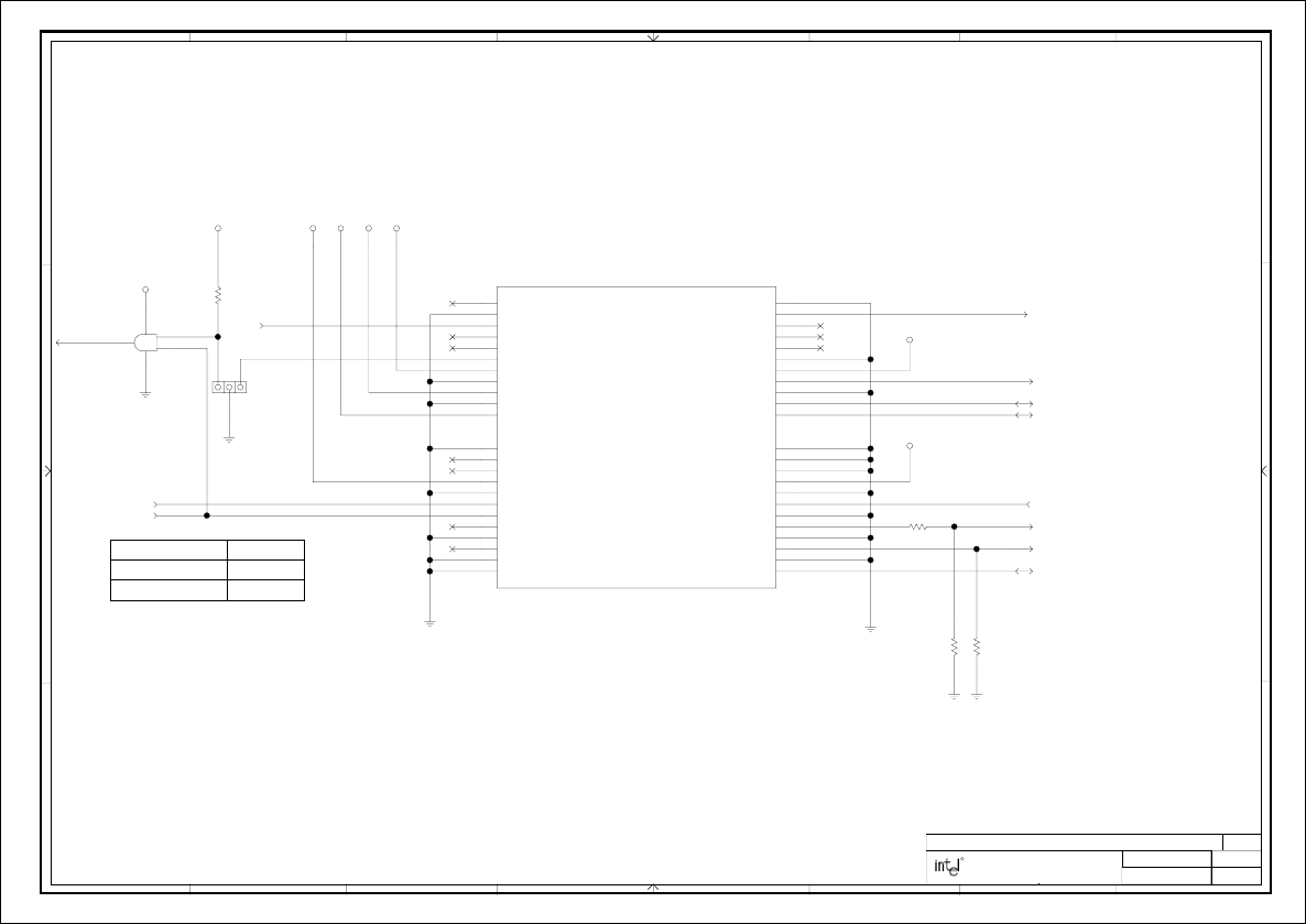
17
AUDIO/MODEM RISER
R125
10K
11,15
AC_BITCLK
11,15
AC_SYNC
15 MONO_OUT
11,15 AC_SDATAOUT
15MONO_PHONE
JP2
3
2
1
PRI_DWN#
PRI_DWN_U
R68
4.7K
25
AC97_USB+
25
AC97_USB-
11 AC_RST#
U3
5
4
6
7
14
15
PRI_DWN_RST#
25
AC97_OC#
J8
A8
A11
A10
B6
A13
A5
A4
A3
B14
B13
B5
B4
A2
B3
A12
A9
A6
B22
B20
B16
B12
B10
B8
A22
A20
A18
A16
A14
B2
A1B1
A17B17
B19
B21
A19
A21
B18
B23 A23
B7 A7
B11
A15B15
B9
AC_SDATAIN1_R R113
AC_SDATAIN0 11,15
AC_SDATAIN1 11
R108
10K
PCD PLATFORM DESIGN
REV:
DRAWN BY:
LAST REVISED:
PROJECT:
SHEET:
FOLSOM, CALIFORNIA 95630
1900 PRAIRIE CITY ROAD
87654321
A
B
C
D
12345678
D
C
B
A
TITLE: INTEL(R) 820 CHIPSET DUAL PROCESSOR CUSTOMER REFERENCE BOARD 3.03
OF 38
R
VCC12-VCC12
VCC3_3SBY
VCC3_3SBY
VCC3_3SBY
VCC5
VCC5VCC3_3
SN74LVC08A
AC’97_RISER
AMR_CONNECTOR
KEY
KEY
KEY
KEY
+12V
+3.3VD +3VDUAL/3VSBY
+5VD
+5VDUAL/5VSBY-12V
AC97_BITCLKAC97_MSTRCLK
AC97_RESET#
AC97_SDATA_IN0
AC97_SDATA_IN1
AC97_SDATA_IN2
AC97_SDATA_IN3
AC97_SDATA_OUT AC97_SYNC
AUDIO_MUTE# AUDIO_PWRDWN
(ISOLATED)GND[0]
GND[10]
GND[11]
GND[12]
GND[13]
GND[14]
GND[1]
GND[2]
GND[3]
GND[4]
GND[5]
GND[6]
GND[7]
GND[8]
GND[9]
MONO_OUT/PC_BEEP
MONO_PHONE
RESV[1]
RESV[2]
RESV[3]
RESV[4]
RESV[5]
RESV[6]
RESV[7]
S/P_DIF_IN
PRIMARY_DN#
USB+
USB-
USB_OC
0K
AC’97 Audio/Modem Riser
Audio Down JP2
Enable* 1-2
Disable 2-3
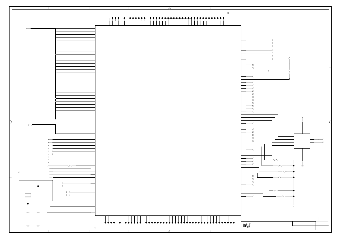
11-29-1999_14:46 18
LAN CONTROLLER
R15
619
TDN 19
10,21,22,23
PCI_PME#
10,22,23
AD[31:0]
AD3
AD4
AD5
AD6
AD7
AD8
AD9
AD10
AD11
AD12
AD13
AD14
AD15
AD16
AD17
AD18
AD19
AD20
AD21
AD22
AD23
AD24
AD25
AD26
AD27
AD28
AD29
AD30
AD31
AD2
AD1
AD0
C_BE#[3:0]
10,22,23 C_BE#0
C_BE#1
C_BE#2
C_BE#3
10,22,23,34 FRAME#
10,22,23,34 IRDY#
10,22,23,34 TRDY#
10,22,23,34 DEVSEL#
10,22,23,34 STOP#
10,22,23 PAR
10,21,22,23,34 PIRQ#A
10,22,23,34 PERR#
PGNT#3
10,34
7PCLK5
25MHZ
Y2
2
1
19
RDP
19
RDN
TDP 19
62K
R363
R14
3.3K
549
R16
R57
3.3K
8,10,12,13,14,21,22,23,24 PCIRST#
19 LAN_RSMRST#
3.3K
R58
3.3K
R59
9,11,31,33 PWROK
10,22,23,34 SERR#
AD20
10,18,22,23 PREQ#3
10,34 100
R75
U5
M13
M9
G2
N11
P11
L11
L6
H11
H10
H9
G11
G10
G9
G8
G7
F11
F10
F9
F8
F7
F6
F5
F4
E11
E10
E9
E8
E7
E6
E5
E4
D11
D8
D7
D6
D5
D4
L9
L10
L5
L4
K11
K10
K9
K8
K7
K6
K5
K4
J11
J10
J9
J8
J7
J6
J5
H8
H7
H6
H5
G6
G5
E12
P2
N6
K3
E1
A7
A3
N1
M6
K2
E2
B7
B3
C10
N12
P8
K12
G14
A11
P12
N8
K13
G13
C13
B11
C11
A12
C12
B13
B14
B12
D12
D14
D13
A13
C8
M8
N9
P7
F14
F13
F12
G12
H14
H13
H12
J14
J13
J12
K14
L14
L13
L12
M14
N14
P13
N13
M12
M11
P10
N10
M10
P9
A6
C5
B10
E14
E13
C14
C9
A10
A9
B9
G1
C2
J3
C3
A4
A2
J2
H2
J1
H1
H3
G3
F1
F2
C4
F3
L3
M4
B8
A8
C7
C6
B6
B5
A5
B4
B2
B1
C1
D3
D2
D1
E3
K1
L2
L1
M3
M2
M1
N2
N3
P3
N4
P4
M5
N5
P5
P6
M7
N7
AUXPWR
EEDI
EEDO
EESK
EECS
FLD5
FLD6
CLKRUN#_LAN
TEST_LAN
RBIAS10
RBIAS100
AD20_RLAN
LAN_X1
LAN_X2
XREF1=19SPEEDLED
19ACTLED
19LILED
U24
8
3
4
2
1
5
6
7
22PF
C101
22PF
C96
11,34 ALERTCLK_SBY
11,34 ALERTDATA_SBY
PCD PLATFORM DESIGN
REV:
DRAWN BY:
LAST REVISED:
PROJECT:
SHEET:
FOLSOM, CALIFORNIA 95630
1900 PRAIRIE CITY ROAD
87654321
A
B
C
D
12345678
D
C
B
A
TITLE: INTEL(R) 820 CHIPSET DUAL PROCESSOR CUSTOMER REFERENCE BOARD 3.03
OF 38
R
VCC3_3SBY
VCC3_3SBY
XTAL
VCC3_3SBY
82559
AD0
AD1
AD2
AD3
AD4
AD5
AD6
AD7
AD8
AD9
AD10
AD11
AD12
AD13
AD14
AD15
AD16
AD17
AD18
AD19
AD20
AD21
AD22
AD23
AD24
AD25
AD26
AD27
AD28
AD29
AD30
AD31
C/BE0#
C/BE1#
C/BE2#
C/BE3#
FRAME#
IRDY#
TRDY#
DEVSEL#
STOP#
PAR
INTA#
PERR#
SERR#
IDSEL
REQ#
GNT#
RST#
CLK
ISOLATE#
ALTRST#
SMBCLK
SMBD
TDN
RDP
RDN
SMBALRT#
CSTSCHG
PME#
FLA16
FLA15/EESK
FLA14/EEDO
FLA13/EEDI
FLA12/MCNTSM#
FLA11/MINT
FLA10/MRING#
FLA9/MRST
FLA8/IOCHRDY
FLA6
FLA5
FLA4
FLA3
FLA2
FLA1/AUXPWR
FLA0/PCIMODE#
FLD7
FLD6
FLD5
FLD4
FLD3
FLD2
FLD1
FLD0
EECS
FLCS#
FLOE#
CLKRUN#
TEST
TEXEC
TCK
TI
TO
RBIAS10
RBIAS100
VREF
LILED
ACTLED
SPEEDLED
TDP
VCCPL[0]
VCCPL[1]
VCCPL[2]
VCCPL[3]
VCCPT
VSSPL[0]
VSSPL[1]
VSSPL[2]
VSSPL[3]
VSSPT
VSSPP[0]
VSSPP[1]
VSSPP[2]
VSSPP[3]
VSSPP[4]
VSSPP[5]
VCCPP[0]
VCCPP[1]
VCCPP[2]
VCCPP[3]
VCCPP[4]
VCCPP[5]
VCC[0]
VCC[1]
VCC[2]
VCC[3]
VCC[4]
VCC[5]
VCC[6]
VCC[7]
VCC[8]
VCC[9]
VCC[10]
VCC[11]
VCC[12]
VCC[13]
VCC[14]
VCC[15]
VCC[16]
VCC[17]
VCC[18]
VCC[19]
VCC[20]
VCC[21]
VCC[22]
VCC[23]
VCC[25]
VCC[24]
VSS[0]
VSS[1]
VSS[2]
VSS[3]
VSS[4]
VSS[5]
VSS[6]
VSS[7]
VSS[8]
VSS[9]
VSS[10]
VSS[11]
VSS[12]
VSS[13]
VSS[14]
VSS[15]
VSS[16]
VSS[17]
VSS[18]
VSS[19]
VSS[20]
VSS[21]
VSS[22]
VSS[23]
VSS[24]
VSS[25]
VSS[26]
VSS[27]
VSS[28]
VSS[29]
VSS[30]
VSS[31]
X2
X1
VIO
FLWE#
FLA7
NC2
NC1
GND
EECS
EESK
EEDO
EEDI VCC
93C46
VCC5SBY
LAN
No stuff R57, R58
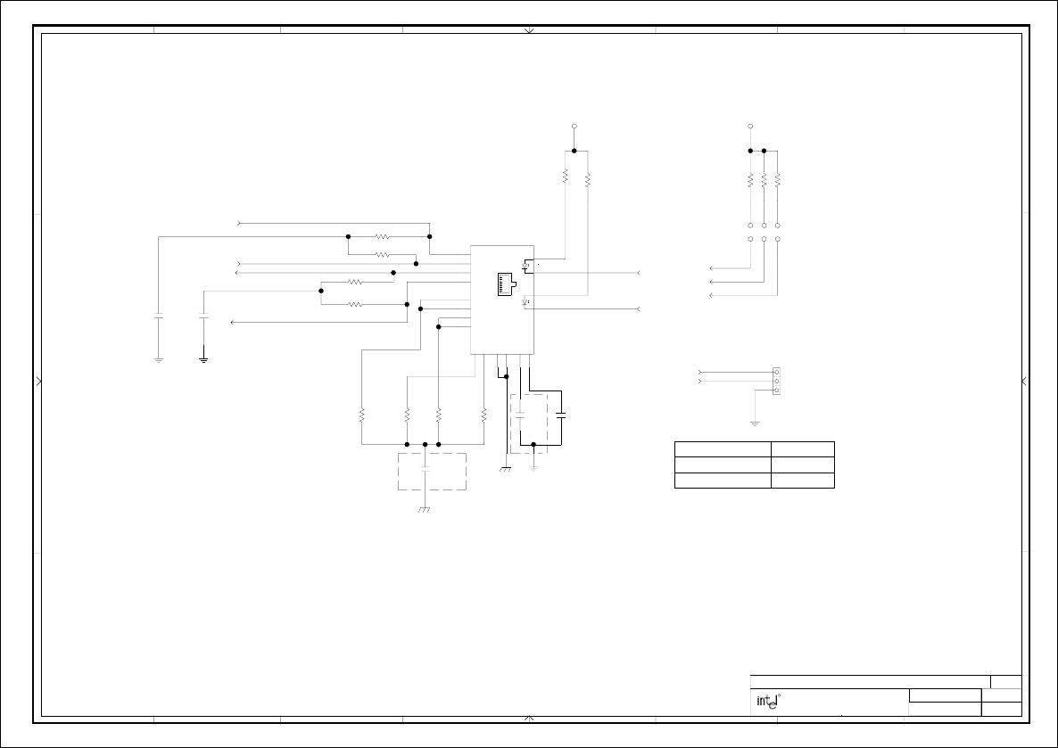
1911-29-1999_14:46
18,19
LILED
18,19
ACTLED
330
R61
R366
330
LILED
18,19
ACTLED
18,19
SPEEDLED
18
LI_J
ACT_J
SPEED_J
JP1
JP4
JP3
R60
330
330
R73
330
R78
18 LAN_RSMRST#
11,33 RSMRST#
TDN
18
18 TDP
J18
3
2
1
RJ4_J
TXC_J
RJ_7_J
RXC_J
LI_CR
ACT_CR
49.9-1%
R26
49.9-1%
R20
75
R6
75
R365
75
R8
75
R10
49.9-1%
R62
49.9-1%
R364
18 RDP
18 RDN
XC_R
TD_C
RD_C
0.1UF
C61
0.1UF
C79
C31
0.1UF
470PF
C5
J2
15
16
13
14
1
2
6
5
4
3
8
11
7
9
12
10
18
17
RDC_J
TDC_J
0.1UF
C78
PCD PLATFORM DESIGN
REV:
DRAWN BY:
LAST REVISED:
PROJECT:
SHEET:
FOLSOM, CALIFORNIA 95630
1900 PRAIRIE CITY ROAD
87654321
A
B
C
D
12345678
D
C
B
A
TITLE: INTEL(R) 820 CHIPSET DUAL PROCESSOR CUSTOMER REFERENCE BOARD 3.03
OF 38
R
VCC3_3 VCC3_3
RJMAG
SHLD1
SHLD2
TD+
TD-
RD+
RD-
TDC
RDC
RJ-4
RJ-5
RJ-7
RJ-8
TXC
RXC
RJ-45
LAN
LAN
For debug only. Hold LAN in reset.
Place termination resistors close to 82559. No stuff JP1,JP3,JP4,R60,R73,R78.
No stuff C61, C79.
No stuff C31.
C5 must be rated at 1500V.
No stuff C5.
82559 LAN J17
Enable* 1-2
Disable 2-3
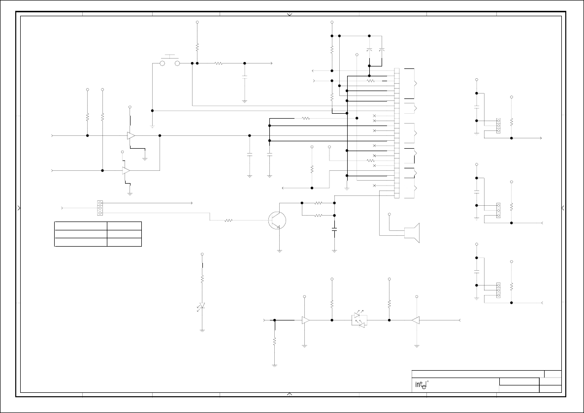
11-29-1999_14:46
SYSTEM
20
GPIO23_FPLED11
U14
14
7
56
U14
43
7
14
R253
330
IRRX
14
1M
R252
SP1
1
2
24 IDEACTS#
24 IDEACTP#
R345
10K
R344
10K
R352
68
R353
68
JP24
1
2
3
JP23
3
2
1
R326
4.7K
JP22
3
2
1
4.7K
R316
14
PWM1
R329
4.7K
R350
2.2K
11 SPKR
P_BEEP
JP25
3
2
115
AC97_SPKR
IDE_ACTIVE
11
PWRBTN#
TACH2
R257
0K
5%
82
R357
14 IRTX
J25
26
25
24
23
22
21
20
19
18
17
16
15
14
13
12
11
10
9
8
7
6
5
4
3
2
1
470
R356
R358
4.7K
5%
KEYLOCK#
14
R355
220
R289
330
CR7
2
1
IRTX_R
HDLED_R
PLED_R
PWRBTN_FP#
SPKR_FP
SPKR_Q
SPKR_ONBOARD
SBY_LED_CR
PC_BEEP
U19
89
7
14
U19
14
7
12
DUAL_COLOR
CR6
12
LED_PU0 LED_PU1
11GPIO26_FPLED
330
R246
4.7K
R234
C267
1UF
470PF
C354
470PF
C355
R359
100K
0.1UF
C327
C316
0.1UF
10K
R354
C322
0.1UF
C350
0.1UF 50V
2
1
C356
10UF 16V
1
2
0.1UF
C353
MMBT3904LT1
Q15
E
C
B
14
PWM2
SW1
PCD PLATFORM DESIGN
REV:
DRAWN BY:
LAST REVISED:
PROJECT:
SHEET:
FOLSOM, CALIFORNIA 95630
1900 PRAIRIE CITY ROAD
87654321
A
B
C
D
12345678
D
C
B
A
TITLE: INTEL(R) 820 CHIPSET DUAL PROCESSOR CUSTOMER REFERENCE BOARD 3.03
OF 38
R
SN74LVC07A
GND
VCC
VCC3_3SBYVCC3_3SBY
SN74LVC07A GND
VCC
VCC3_3
VCC3_3SBY
VCC5
VCC3_3SBY
VCC3_3
VCC3_3
VCC3_3
VCC5
NEG
POS
+
VCC5
VCC5
VCC12
VCC12
VCC12
VCC3_3
FNT_PNL_CONN
VCC3_3
VCC5
VCC3_3
SN74LVC07A GND
VCC
VCC3_3SBY
SN74LVC07A GND
VCC
VCC3_3SBY
+
+
13
2
KEY
KEY
No stuff.
For test only
No stuff.
KEY
INFRARED
H.D. LED
PWM1
TACH2
PWM2
SPEAKER
POWER SW.
For test only
ICH has internal pullup and debounce on PWRBTN#
KEY
Speaker Circuit
KEY
KEY
KEYLOCK
POWER LED
Onboard LED indicates the standby well is on
PWM outputs from SIO need power buffers for driving fan inputs.
to prevent hot swapping memory.
For debug only.
System
Onboard Spkr JP25
Enable* 2-3
Disable 1-2
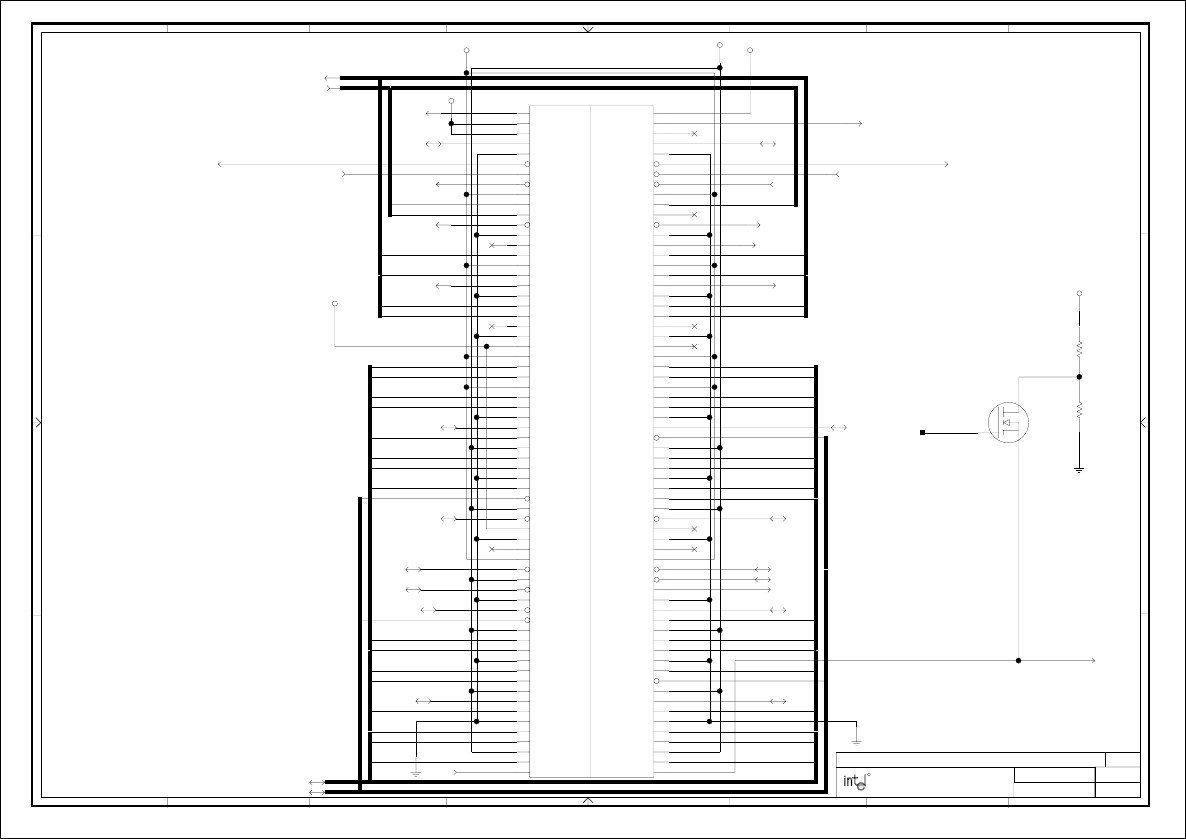
11-30-1999_10:10
AGP CONNECTOR
21
21,31 TYPEDET#
R208
200-1%
9 GAD[31:0]
GAD0
GAD2
GAD4
GAD6
GAD9
GAD11
GAD13
GAD15
GAD16
GAD18
GAD20
GAD22
GAD24
GAD26
GAD28
GAD30
GAD1
GAD3
GAD5
GAD7
GAD8
GAD10
GAD12
GAD14
GAD17
GAD19
GAD21
GAD23
GAD25
GAD27
GAD29
GAD31
25 AGP_OC#
7AGPCLK_CONN
9,34 GREQ#
ST0 ST1
ST2
9ST[2:0]
9,34 RBF#
SBA0
SBA2
SBA4
SBA6
SBA5
SBA7
SBA3
SBA1
9
SBA[7:0]
9,34 SBSTB
9,34 ADSTB1
GC/BE#2
GC/BE#0
GC/BE#3
GC/BE#1
9 GC/BE#[3:0]
9,34 GIRDY#
9,34 GDEVSEL#
34 GPERR#
34 GSERR#
9,34 ADSTB0 9,34ADSTB#0
9,34GPAR
10,18,22,23
PCI_PME# 9,34
GSTOP# 9,34
GTRDY#
9,34
GFRAME#
9,34
ADSTB#1
9,34
SBSTB#
9,34
WBF#
9,34
PIPE#
9,34
GGNT# 8,10,12,13,14,18,22,23,24
PCIRST#
25
USBAGP-
21,31
TYPEDET#
10,18,22,23,34
PIRQ#A
10,22,23,34 PIRQ#B
R193
301-1%
25 USBAGP+
8MCH_AGPREF
8
CONN_AGPREF
CON_AGPREF_Q
Q8
2
3
1
J13
B42
B24
A66B66
B65
B64
B63
B62
B61
B60
B59
B58
B57
B56
B55
B54
B53
B52
B51
B50
A65
A64
A63
A62
A61
A60
A59
A58
A57
A56
A55
A54
A53
A52
A51
A50
B49
B48
A49
A48
A47
A46
A45
A44
A43
A42
A41
B47
B46
B45
B44
B43
B41
A35
A36
A37
A38
A39
A40B40
B39
B38
B37
B36
B35
B34 A34
A33
A32
A31
A30
A29
A28
A27
A26
B33
B32
B31
B30
B29
B28
B27
B26
B16
B25 A25
A24
B23
B22
A23
A22
B21 A21
A20
A19
A18
A17
A16
A15
A14
A13
A12
B14
A11
A10
A9
A8
A7
A6
A5
A4
A3
A2
A1
B20
B19
B18
B17
B15
B13
B12
B11
B10
B9
B8
B7
B6
B5
B4
B3
B2
B1
PCD PLATFORM DESIGN
REV:
DRAWN BY:
LAST REVISED:
PROJECT:
SHEET:
FOLSOM, CALIFORNIA 95630
1900 PRAIRIE CITY ROAD
87654321
A
B
C
D
12345678
D
C
B
A
TITLE: INTEL(R) 820 CHIPSET DUAL PROCESSOR CUSTOMER REFERENCE BOARD 3.03
OF 38
R
VDDQ
VDDQ
VCC3_3 VCC12
VCC3_3SBY
VCC5
2N7002LT1
1
3
2
AGP4XU_20
OVRCNT#
5V_A
5V_B
USB+
GND_K
INTB#
CLK
REQ#
VCC3_3_F
ST0
ST2
RBF#
GND_L
SBA0
SBA2
SB_STB
GND_M
SBA4
12V
TYPEDET#
RESV_A
USB-
GND_A
INTA#
RST#
GNT#
VCC3_3_A
ST1
RESV_B
RESV_H
PIPE#
GND_B
WBF#
SBA1
VCC3_3_B
SBA3
SB_STB#
GND_C
SBA5
SBA7
SBA6
RESV_C
GND_D
RESV
GND_N
RESV_D
VCC3_3_C
VCC3_3_H
VCC3_3_G
AD31
AD29
VCC3_3_I
AD27
AD25
GND_O
AD_STB1
AD23
AD30
AD28
VCC3_3_D
AD26
AD24
GND_E
AD_STB1#
C/BE3#
VDDQ_A
VDDQ_F
AD21
AD19
GND_P
AD17
C/BE2#
VDDQ_G VDDQ_B
AD16
AD18
GND_F
AD20
AD22
IRDY#
GND_Q
RESV_K
VCC3_3_J
DEVSEL#
VDDQ_H
FRAME#
RESV_E
GND_G
RESV_F
VCC3_3_E
TRDY#
STOP#
PME#
GND_H
PERR#
GND_R
PAR
AD15
VDDQ_C
AD13
AD11
GND_I
AD9
C/BE0#
VDDQ_D
AD_STB0#
AD6
GND_J
AD4
AD2
VDDQ_E
AD0
SERR#
C/BE1#
VDDQ_I
AD14
AD12
GND_S
AD10
AD8
VDDQ_J
AD_STB0
AD7
GND_T
AD5
AD3
VDDQ_K
AD1
VREF_CG VREF_GC
3_3VAUX1
3_3VAUX2
AGPREF circuitry should be placed close to MCH.
AGP Connector
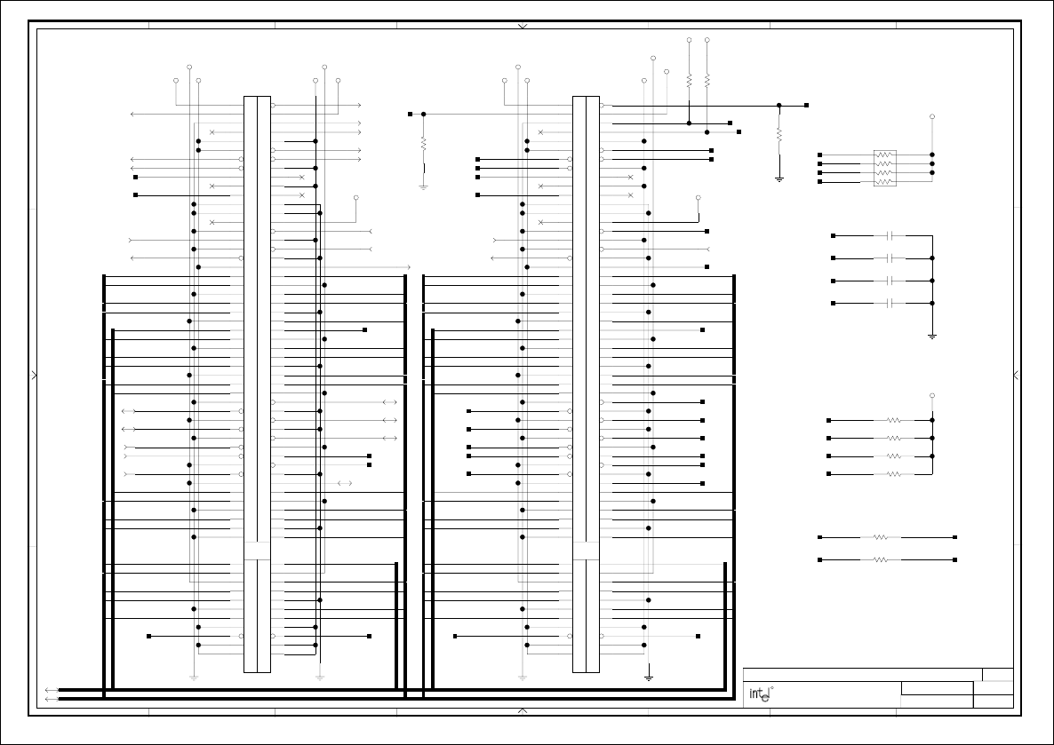
PCI CONNECTORS 1 AND 2
11-29-1999_14:46 22
22,23 PTCK
10,21,22,23,34 PIRQ#B
10,22,23,34 PIRQ#D
7PCLK1
10,34 PREQ#0
C_BE#1
C_BE#0
C_BE#2
C_BE#3
C_BE#0
C_BE#3
C_BE#2
C_BE#1
10,18,23 C_BE#[3:0]
10,18,22,23,34 IRDY#
10,18,22,23,34 DEVSEL#
10,22,23,34 PLOCK#
10,18,22,23,34 SERR#
10,18,22,23PAR
10,18,22,23,34
TRDY#
10,18,22,23,34
FRAME#
10,22,23,34
PIRQ#C 10,18,21,22,23,34
PIRQ#A
22,23
PTDI 22,23
PTMS 22,23 PTCK
10,34
PGNT#1
10,34 PREQ#1
7PCLK2
22 SDONEP1
22 SDONEP2
22 SBOP1
22 SBOP2
22 PRSNT#11
22 PRSNT#12
22 PRSNT#21
22 PRSNT#22
22 PU1_ACK64#
22 PU1_REQ64#
22 PU2_ACK64#
22 PU2_REQ64#
22
R_AD16
22
R_AD17
22,23
PTRST#
5.6K
R74
5.6K
R367
5.6K
R79
5.6K
R72
100
R120
100
R119
5.6K
RP12 8
7
6
54
3
2
1
2.7K
R178
2.7K
R179
2.7K
R176
2.7K
R177
22,23
PTDI 22,23
PTMS
10,18,22,23,34
STOP#
10,18,21,22,23PCI_PME#
8,10,12,13,14,18,21,22,23,24
PCIRST#
10,34
PGNT#0
22
R_AD17
22 PRSNT#11
22 PRSNT#12
10,18,22,23,34 PERR#
22
SBOP1 22
SDONEP1
IRDY#
DEVSEL#
PLOCK#
SERR#
22
R_AD16
22,23
PTRST#
22 PRSNT#21
22 PRSNT#22
8,10,12,13,14,18,21,22,23,24
PCIRST#
10,18,21,22,23
PCI_PME#
FRAME#
TRDY#
STOP#
SDONEP2
SBOP2
PAR
10,18,22,23 AD16
10,18,22,23 AD17
PERR#
10,21,22,23,34
PIRQ#B
10,22,23,34
PIRQ#D
10,22,23,34 PIRQ#C
10,18,21,22,23,34 PIRQ#A
AD25
10,18,23 AD[31:0]
AD30
AD3
AD5
AD7
AD17
AD31
AD29
AD27
AD25
AD23
AD19
AD14
AD12
AD10
AD8
AD1
AD2
AD4
AD6
AD9
AD11
AD13
AD15
AD16
AD18
AD20
AD22
AD24
AD26
AD30
AD28
AD0AD0
AD28
AD26
AD24
AD22
AD20
AD18
AD13
AD11
AD9
AD6
AD4
AD2
AD1
AD10
AD12
AD14
AD19
AD21
AD23
AD27
AD29
AD31
AD17
AD7
AD5
AD3
AD8
AD16
AD15
AD21
22
PU2_REQ64#
22 PU2_ACK64#
22
PU1_REQ64#
22 PU1_ACK64#
0.1UF
C117
0.1UF
C123
0.1UF
C113
0.1UF
C122
J11
A2
A21
A27
A33
A39
A45
B25
B31
B36
B43
A53
B54
A5
A8
A10
A16
B5
B6
A59
A61
A62
B59
B61
B62
B19
B1
B60
A58B58
B48
A47B47
A46
B45
A44
A32B32
A31
B30
A57
A29B29
A28
B27
A25
B24
A23B23
A22
B21
B56
A20B20
A55B55
A54
B53
B52
A49
A52
B44
B33
B26
B16
A9
B37
A34
A12
A13
A18
A24
A30
A35
A37
A42
A48
B3
B12
B13
B15
B17
B22
B34
B38
B46
B49
A56
B57
B28
A17
A26
A6
B7 A7
B8
B35
B39
A43
B40
A19
B9
B11
B2
B4 A4
A3
A1
B18
A60
A11
A14
B10
B14
A15
A41
A40
B42
A38
A36
B41
J12
B41
A36
A38
B42
A40
A41
A15
B14
B10
A14
A11
A60
B18
A1
A3
A4B4
B2
B11
B9
A19
B40
A43
B39
B35
B8
A7B7
A6
A26
A17
B28
B57
A56
B49
B46
B38
B34
B22
B17
B15
B13
B12
B3
A48
A42
A37
A35
A30
A24
A18
A13
A12
A34
B37
A9
B16
B26
B33
B44
A52
A49
B52
B53
A54
B55 A55
B20 A20
B56
B21
A22
B23 A23
B24
A25
B27
A28
B29 A29
A57
B30
A31
B32 A32
A44
B45
A46
B47 A47
B48
B58 A58
B60
B1
B19
B62
B61
B59
A62
A61
A59
B6
B5
A16
A10
A8
A5
B54
A53
B43
B36
B31
B25
A45
A39
A33
A27
A21
A2
PCD PLATFORM DESIGN
REV:
DRAWN BY:
LAST REVISED:
PROJECT:
SHEET:
FOLSOM, CALIFORNIA 95630
1900 PRAIRIE CITY ROAD
87654321
A
B
C
D
12345678
D
C
B
A
TITLE: INTEL(R) 820 CHIPSET DUAL PROCESSOR CUSTOMER REFERENCE BOARD 3.03
OF 38
R
VCC3_3SBY
VCC5
VCC5VCC5
VCC5VCC5VCC5VCC5VCC12-
VCC3_3 VCC3_3
VCC12
VCC3_3
VCC12-
VCC12
VCC3_3
VCC5
VCC3_3SBY
PCI3_CON
key
PCI3_CON
key
PCI Slot 0
For pullups, see 4.3.3 of PCI 2.1 Specification
PCI Slot 1
0 and 1
PCI Connectors
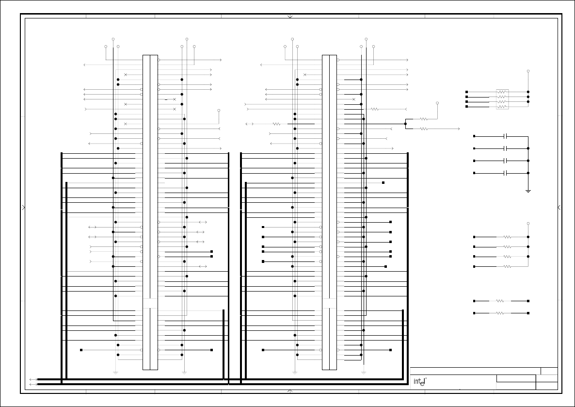
PCI CONNECTORS 3 AND 4
11-29-1999_14:46 23
VAUX_JP
R110
R107
SDONEP3
23 SDONEP4
23 SBOP3
23 SBOP4
23
PRSNT#31
23
PRSNT#32
23
PRSNT#41
23
PRSNT#42
23
PU3_ACK64#
23
PU3_REQ64#
23
PU4_ACK64#
23
PU4_REQ64#
23
AD23
10,18,22,23
AD22
10,18,22,23
R_AD23
R_AD22 23
7PCLK4
23
R_AD22
PCIRST# 8,10,12,13,14,18,21,22,23,24
FRAME# 10,18,22,23,34
PTCK
22,23
PCLK3
7
IRDY#
10,18,22,23,34
DEVSEL#
10,18,22,23,34
PLOCK#
10,22,23,34 PERR#
10,18,22,23,34
SERR#
10,18,22,23,34
STOP# 10,18,22,23,34
TRDY# 10,18,22,23,34
PCI_PME# 10,18,21,22,23
C_BE#1
C_BE#0
C_BE#2
C_BE#3
C_BE#[3:0]10,18,22
C_BE#3
C_BE#2
C_BE#1
C_BE#0
R118
100
R117
100
RP13
5.6K
8
7
6
54
3
2
1
R174
2.7K
R175
2.7K
R172
2.7K
R173
2.7K
PTMS 22,23
PTRST# 22,23
PTDI 22,23
PRSNT#31
23
PRSNT#32
23
PAR 10,18,22,23
10,22,23,34 PIRQ#D
10,21,22,23,34 PIRQ#B
23 PRSNT#41
23 PRSNT#42
22,23
PTRST#
8,10,12,13,14,18,21,22,23,24
PCIRST#
10,18,21,22,23
PCI_PME#
IRDY#
DEVSEL#
PLOCK#
PERR#
SERR#
PAR
23
SBOP4 23
SDONEP4
STOP#
TRDY#
FRAME#
10,18,21,22,23,34
PIRQ#A 10,22,23,34
PIRQ#C
22,23
PTDI 22,23
PTMS
22,23 PTCK
PREQ#2
10,34
10,34
PGNT#2
PIRQ#B
10,21,22,23,34
PIRQ#D 10,22,23,34
PIRQ#A
10,18,21,22,23,34 PIRQ#C
10,22,23,34
10,34
PGNT#5
10,34 PREQ#5
10,14,34 SERIRQ
11 PCI_TEST
R255
10,34GNT#A
10,34REQ#A
GNT#A_R
SERIRQ_R
R99
23 PU3_ACK64# 23
PU3_REQ64# 23 PU4_ACK64# 23
PU4_REQ64#
C112 0.1UF
C121 0.1UF
C116 0.1UF
C126 0.1UF
J9
A2
A21
A27
A33
A39
A45
B25
B31
B36
B43
A53
B54
A5
A8
A10
A16
B5
B6
A59
A61
A62
B59
B61
B62
B19
B1
B60
A58B58
B48
A47B47
A46
B45
A44
A32B32
A31
B30
A57
A29B29
A28
B27
A25
B24
A23B23
A22
B21
B56
A20B20
A55B55
A54
B53
B52
A49
A52
B44
B33
B26
B16
A9
B37
A34
A12
A13
A18
A24
A30
A35
A37
A42
A48
B3
B12
B13
B15
B17
B22
B34
B38
B46
B49
A56
B57
B28
A17
A26
A6
B7 A7
B8
B35
B39
A43
B40
A19
B9
B11
B2
B4 A4
A3
A1
B18
A60
A11
A14
B10
B14
A15
A41
A40
B42
A38
A36
B41
J10
B41
A36
A38
B42
A40
A41
A15
B14
B10
A14
A11
A60
B18
A1
A3
A4B4
B2
B11
B9
A19
B40
A43
B39
B35
B8
A7B7
A6
A26
A17
B28
B57
A56
B49
B46
B38
B34
B22
B17
B15
B13
B12
B3
A48
A42
A37
A35
A30
A24
A18
A13
A12
A34
B37
A9
B16
B26
B33
B44
A52
A49
B52
B53
A54
B55 A55
B20 A20
B56
B21
A22
B23 A23
B24
A25
B27
A28
B29 A29
A57
B30
A31
B32 A32
A44
B45
A46
B47 A47
B48
B58 A58
B60
B1
B19
B62
B61
B59
A62
A61
A59
B6
B5
A16
A10
A8
A5
B54
A53
B43
B36
B31
B25
A45
A39
A33
A27
A21
A2
23
SDONEP3
23
SBOP3
AD1
AD3
AD5
AD7
AD8
AD14
AD30
AD28
AD26
AD24
AD22
AD20
AD18
AD16
AD15
AD13
AD9
AD6
AD4
AD2
AD0
AD17
AD19
AD21
AD23
AD25
AD27
AD29
AD31
AD[31:0]10,18,22
AD11
AD3
AD5
AD7
AD17
AD31
AD29
AD27
AD25
AD23
AD21
AD19
AD14
AD12
AD10
AD8
AD1
AD2
AD4
AD6
AD9
AD11
AD13
AD15
AD16
AD18
AD20
AD22
AD26
AD28
AD0
AD10
AD12
AD30
AD24
PCD PLATFORM DESIGN
REV:
DRAWN BY:
LAST REVISED:
PROJECT:
SHEET:
FOLSOM, CALIFORNIA 95630
1900 PRAIRIE CITY ROAD
87654321
A
B
C
D
12345678
D
C
B
A
TITLE: INTEL(R) 820 CHIPSET DUAL PROCESSOR CUSTOMER REFERENCE BOARD 3.03
OF 38
R
0K
0K
VCC5
VCC5
VCC12
VCC3_3
VCC5VCC5VCC12-VCC12-
VCC3_3
VCC5 VCC5
VCC3_3
VCC12
VCC3_3
VCC3_3SBY
0K
VCC3_3SBY
0K
PCI3_CON
key
PCI3_CON
key
PCI Slot 2 PCI Slot 3
GNT#A for debug only
J9 must be furthest from the processor.
2 and 3
PCI Connectors
SERIRQ for debug only
REQ#A for debug only
No Stuff R110.
PCI_TEST for debug only
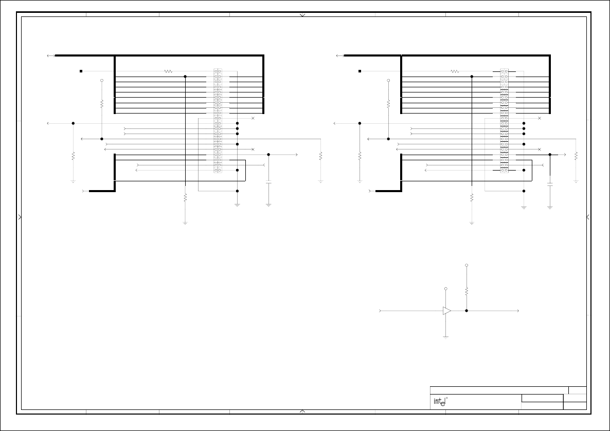
11-29-1999_14:46
IDE CONNECTORS
24
12S66DETECT
C318
0.047UF
12P66DETECT
24
PCIRST_BUF#
8,10,12,13,14,18,21,22,23 PCIRST#
11 SDCS#1
10,34 IRQ15
11 PDREQ
11 PIORDY
10,34 IRQ14
11 PDCS#1
11 PDIOW# 11 SDIOW#
11 SDIOR#
11 SDREQ
33
R333
1K
R336
5.6K
R335
10K
R334
470
R337
1K
R321
33
R318
5.6K
R320
10K
R319
470
R322
11
SDCS#3
11
PDCS#3
11 PDD[15:0]
PDD8
PDD9
PDD10
PDD11
PDD12
PDD13
PDD14
PDD15
PDD1
PDD0
PDD2
PDD3
PDD4
PDD5
PDD6
PDD7
11 SDA[2:0]
SDA2
SDA0
SDA1
11 SDD[15:0]
SDD9
SDD10
SDD11
SDD12
SDD13
SDD14
SDD15
SDD1
SDD0
SDD2
SDD3
SDD4
SDD5
SDD6
SDD7 SDD8
24 PCIRST_BUF#
J22
9
87
65
40
4
39
3837
3635
3433
3231
30
3
29
2827
2625
2423
2221
20
2
19
1817
1615
1413
1211
10
1
J21
1
10
11 12
13 14
15 16
17 18
19
2
20
21 22
23 24
25 26
27 28
29
3
30
31 32
33 34
35 36
37 38
39
4
40
56
78
9
24 PCIRST_BUF#
8.2K
R351
20 IDEACTP#
PDA2
PDA1
11 PDA[2:0]
PDA0
20 IDEACTS#
11 PDIOR#
11 PDDACK# 11 SIORDY
11 SDDACK#
PCIRST#_RS
IDE_JSIDE_JP
PCIRST#_RP
U19
56
7
14
C329
0.047UF
PCD PLATFORM DESIGN
REV:
DRAWN BY:
LAST REVISED:
PROJECT:
SHEET:
FOLSOM, CALIFORNIA 95630
1900 PRAIRIE CITY ROAD
87654321
A
B
C
D
12345678
D
C
B
A
TITLE: INTEL(R) 820 CHIPSET DUAL PROCESSOR CUSTOMER REFERENCE BOARD 3.03
OF 38
R
VCC5VCC5
VCC3_3
VCC3_3
SN74LVC07A GND
VCC
Secondary IDE
Primary IDE
For drive side detection, stuff C329,C318.
For host side detection, no stuff C329,C318.
P66DETECT and S66DETECT can be connected to a GPI for BIOS cable detection.
IDE Connectors
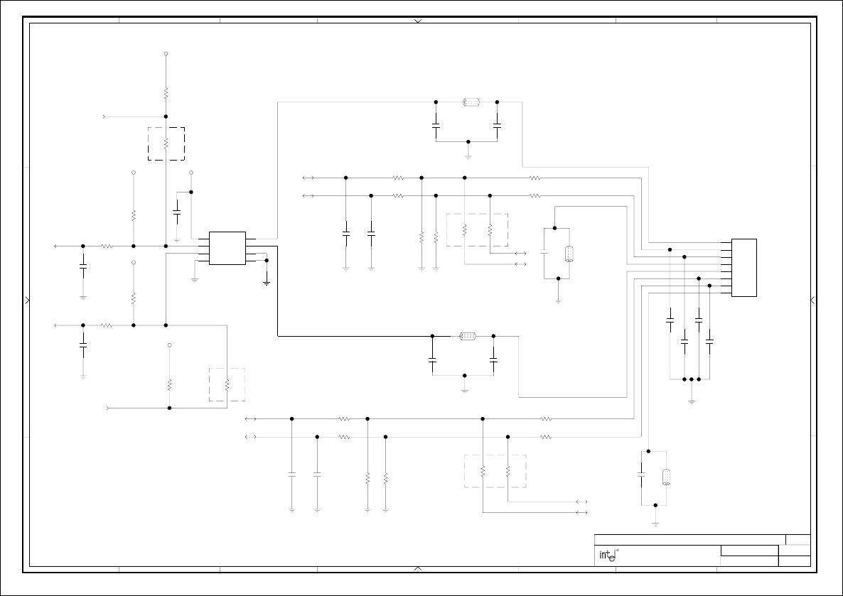
11-29-1999_14:46
USB CONNECTORS
25
R378
0K
R377
0K
USBV0
USBV1
USBD1N
USBD1P
USBG1
10K
R97
11 OC#0
R83
330K
AC97_OC#
17
R48
0K
R50
0K
USBP1N_R
USBP1P_R
4.7K
R91
21
USBAGP+
R41
0K
R42
0K
11 USBP0N
11 USBP0P
11 USBP1P
15-1%
R240
15-1%
R242
15
R244
15K
R45
15K
R43
AGP_OC#
21
R368
330K
21
USBAGP-
15
R243
0K
R44
L11 12
L10
21
L7
2
1
L6
1
2
U7
4
3
6
7
8
2
1
5
USBPWR2_F
R49
15K
17AC97_USB-
17
AC97_USB+
R82
0K
11 USBP1N
R86
4.7K
10K
R87
11 OC#1
OC#0_RC
OC#1_RC
USBPWR1_F
USB_STK
J3
7
6
5
4
3
2
8
1
C120
0.1UF
0.1UF
C102
C109
0.1UF
C239
47PF 47PF
C241
68UF-TANT
C99
0.1UF
C44
47PF
C42
47PF
C41
47PF
C40
C39 47PF
68UF-TANT
C98
0.1UF
C43
470PF
C37
C38
470PF
47PF
C244
47PF
C245
15K
R47
R88
0K
USBG0
USBD0N_R
0K
R46
USBD0P_R
USBD0N
USBD0P
PCD PLATFORM DESIGN
REV:
DRAWN BY:
LAST REVISED:
PROJECT:
SHEET:
FOLSOM, CALIFORNIA 95630
1900 PRAIRIE CITY ROAD
87654321
A
B
C
D
12345678
D
C
B
A
TITLE: INTEL(R) 820 CHIPSET DUAL PROCESSOR CUSTOMER REFERENCE BOARD 3.03
OF 38
R
VCC3_3
VCC3_3 OC#2
GND
IN
OC#1
OUT1
OUT2
EN#1
EN#2
TPS2042
VCC3_3
VCC5VCC3_3
VCC0
GND1
DATA0-
DATA0+
GND0
VCC1
DATA1-
DATA1+
Do Not
Stuff
15 ohm resistors and 47pf caps should be within 1" of ICH
Do Not
Stuff
Do Not
Stuff
Do Not
Stuff
C98, C99 must have low ESR.
USB Connectors
Place caps close to connector.
C39-C42 for test and debug only.

11-29-1999_14:46
PARALLEL PORT
26
PDR7_R
PDR6_R
PDR5_R
PDR4_R
PDR3_R
SLIN#_R
PDR2_R
PAR_INIT#_R
VCC5_DB25_CR
SLCT
14
PE
14
BUSY
14
ACK#
14
SLIN#
14
J6
P15
P16
P13
P23
P10
P25
P12
P24
P11
P22
P9
P21
P8
P20
P7
P19
P6
P18
P5
P17
P4
P3
P2
P14
P1
14 STB#
2.2K
R40
33
RP18
1
2
3
45
6
7
8
33
RP19 8
7
6
54
3
2
1
14 PAR_INIT#
14 ERR#
PDR0_R
STB#_R
180PF C81
180PF CP2
63
180PF CP2
45
180PF CP2
18
180PF CP2
72
RP20
33
1
2
3
45
6
7
8
14 AFD#
PDR0
PDR1
14
PDR[7:0]
PDR4
PDR5
PDR6
PDR7
PDR3
PDR2
180PF
CP5
54
180PF
CP5
36
180PF
CP5
72
180PF
CP5
18
RP4
2.2K
1234
5678
PDR1_R
RP1
2.2K
8765
4321
AFD#_R
180PF
CP3
18
180PF
CP3
72 CP3 180PF
63
180PF
CP3
45
RP2
2.2K
1234
5678
RP3
2.2K
8765
4321
180PF
CP4
45
CP4 180PF
63
180PF
CP4
27
180PF
CP4
81
MMBD914LT1
CR1 31
PCD PLATFORM DESIGN
REV:
DRAWN BY:
LAST REVISED:
PROJECT:
SHEET:
FOLSOM, CALIFORNIA 95630
1900 PRAIRIE CITY ROAD
87654321
A
B
C
D
12345678
D
C
B
A
TITLE: INTEL(R) 820 CHIPSET DUAL PROCESSOR CUSTOMER REFERENCE BOARD 3.03
OF 38
R
DB25_DB9_STK
VCC5
Parallel Port
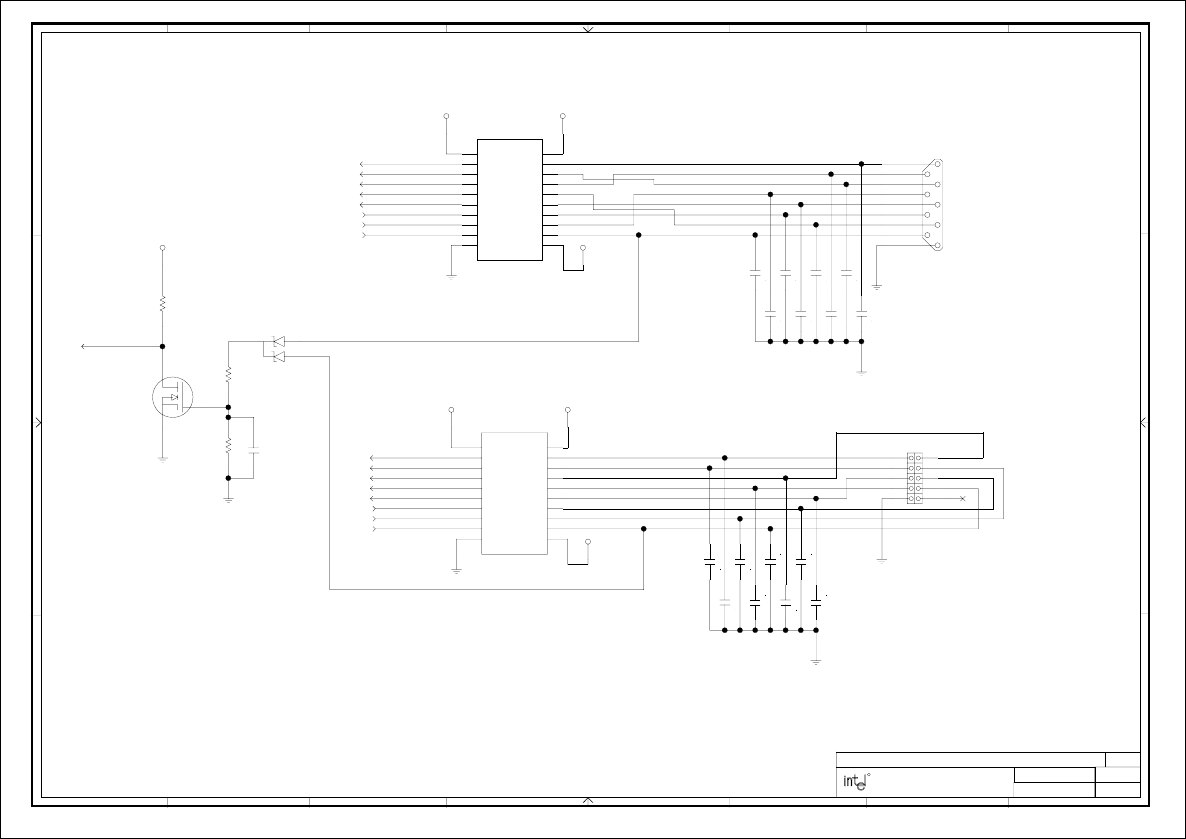
11-29-1999_14:46
SERIAL PORTS
27
CTS1_C
DTR1_C
DCD1_C
RTS0_C
DTR0_C
RXD0_C
DSR0_C
TXD1_C
RXD1_C
RTS1_C
U6
19
18
17
15
14
13
12
11
1
2
3
4
5
6
7
8
9
10
16
20
TXD1
14
14 DCD#1
14 RTS#1
14 RXD1
14 CTS#1
14 RI#1
14 DSR#1
14 DTR#1
DCD0_C
CTS0_C
TXD0_C
14 DTR#0
14 DSR#0
14 RI#0
14 CTS#0
14 RXD0
14 RTS#0
14 DCD#0
TXD0
14
U4
20
16
10
9
8
7
6
5
4
3
2
1
11
12
13
14
15
17
18
19
RI0_C
11 ICH_RI#
J6
A5
A9
A4
A8
A3
A7
A2
A6
A1
J7
4
9
87
65
3
2
10
1
DSR1_C
R69
47K
RI_Q
47K
R70
10K
R369
RI_CR
CR2
1
2
3
1UF
C92
CP1
100PF
36
100PF CP8
45
CP8
100PF
72
CP8
100PF
36
100PF CP1
45
100PF CP8
18
100PF CP1
81 CP1
100PF
72
100PF CP7
81 100PF
CP6
45
CP7
100PF
54
100PF CP7
36
CP6 100PF
81 100PF
CP6
27
100PF
CP6
63
Q1
1
3
2
100PF CP7
72
RI1_C
PCD PLATFORM DESIGN
REV:
DRAWN BY:
LAST REVISED:
PROJECT:
SHEET:
FOLSOM, CALIFORNIA 95630
1900 PRAIRIE CITY ROAD
87654321
A
B
C
D
12345678
D
C
B
A
TITLE: INTEL(R) 820 CHIPSET DUAL PROCESSOR CUSTOMER REFERENCE BOARD 3.03
OF 38
R
VCC12-
VCC5 VCC12
RY0
RY1
RY2
DA1
RY3
DA2
RY4
GND
VCC12
RA0
RA1
RA2
DY0
DY1
RA3
DY2
RA4
VCC-12
DA0
VCC
GD75232
RY0
RY1
RY2
DA1
RY3
DA2
RY4
GND
VCC12
RA0
RA1
RA2
DY0
DY1
RA3
DY2
RA4
VCC-12
DA0
VCC
GD75232
VCC12VCC5
VCC12-
DB25_DB9_STK
DCD
DSR
RXD
RTS
TXD
CTS
DTR
RI
GND
VCC3_3SBY
BAT54C
2N7002LT1
1
3
2
COM2 is a 2x5 pin header for a cabled port.
COM1
COM2
Serial Ports
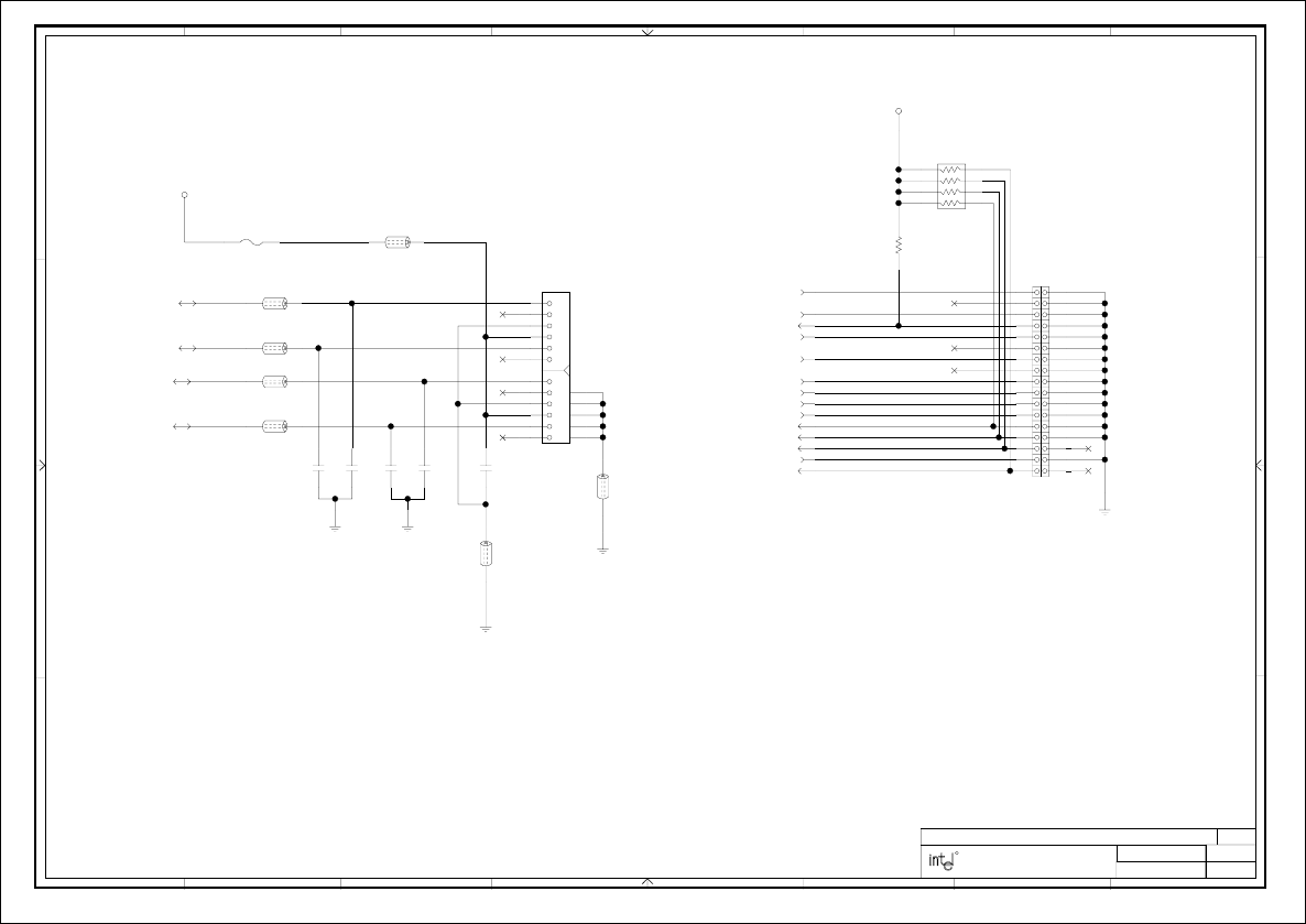
11-29-1999_14:46 28
KEYBOARD/MOUSE/FLOPPY
RDATA#
14
TRK#0
14
DSKCHG#
14
HDSEL#
14
WGATE#
14
WDATA#
14
STEP#
14
DIR#
14
DS#0
14
MTR#0
14
14 INDEX#
DRVDEN#1
14
DRVDEN#0
14
L13
12
L14
21
L12
21
L16
12
14 KBCLK
14 KBDAT
RP17
1K
1
2
3
45
6
7
8
J23
1
10
1112
1314
1516
1718
19
2
20
2122
2324
2526
2728
29
3
30
4
56
78
9
3132
3334
14 MDAT
14 MCLK
F1 21
R328
1K
L15
21
L9
2
1
L8
1
2
VCC5_KBMS_F 14VCC5_KBMS_J
GND_KBMS_FB
KBCLK_FB
MDAT_FB
MCLK_FB
GND_KBMS_C
J1
9
8
7
6
5
4
3
2
17
16
15
14
1312
11
10
1
KBDAT_FB
100PF
C45
100PF
C33
100PF
C32
100PF
C46
0.1UF
C47
WRTPRT#
14
PCD PLATFORM DESIGN
REV:
DRAWN BY:
LAST REVISED:
PROJECT:
SHEET:
FOLSOM, CALIFORNIA 95630
1900 PRAIRIE CITY ROAD
87654321
A
B
C
D
12345678
D
C
B
A
TITLE: INTEL(R) 820 CHIPSET DUAL PROCESSOR CUSTOMER REFERENCE BOARD 3.03
OF 38
R
VCC5
VCC5
1.0A
PS/2 KybdPS/2 Mse
Floppy Connector
Keyboard/Mouse/Floppy
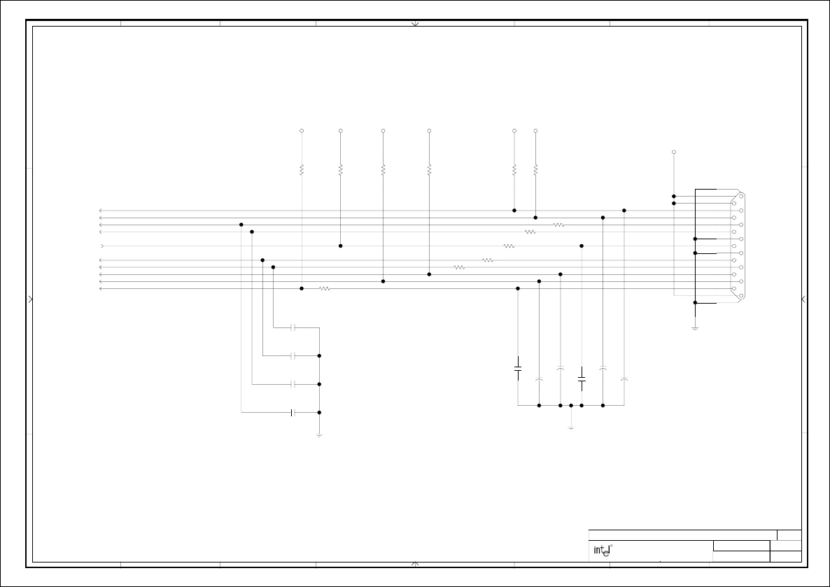
GAME PORT
29
4.7K
R35
4.7K
R39
47
R38
1K
R33
1K
R32
R36
1K
R37
1K
14 MIDI_IN
14 J1BUTTON2
14 J2BUTTON2 5%
R24
2.2K
5%2.2K
R23 47
R34 5%2.2K
R22 5%2.2K
R21
14 JOY2Y
14 JOY1Y
14 MIDI_OUT
14 JOY2X
14 JOY1X
14 J1BUTTON1
14 J2BUTTON1
JOY1X_R
JOY2X_R
MIDI_OUT_R
JOY2Y_R
JOY1Y_R
MIDI_IN_R
J5
2
10
3
11
4
12
5
13
6
14
7
15
8
1
9
31
32
0.01UF
C69
25V
10%
10%
25V
C68
0.01UF
0.01UF
C67
25V
10%
0.01UF
C66
25V
10%
50V
C51
47PF
1
2
50V
C52
47PF
2
1
50V
47PF
C54
1
2
50V
C55
47PF
2
1
470PF
C53
C56
470PF
PCD PLATFORM DESIGN
REV:
DRAWN BY:
LAST REVISED:
PROJECT:
SHEET:
FOLSOM, CALIFORNIA 95630
1900 PRAIRIE CITY ROAD
87654321
A
B
C
D
12345678
D
C
B
A
TITLE: INTEL(R) 820 CHIPSET DUAL PROCESSOR CUSTOMER REFERENCE BOARD 3.03
OF 38
R
VCC5VCC5 VCC5 VCC5 VCC5 VCC5
VCC5
DB15_AUD_STK
+
+
+
+
Tie game port capacitors together and to SIO AVSS. Tie to system ground at only a single point.
Game Port
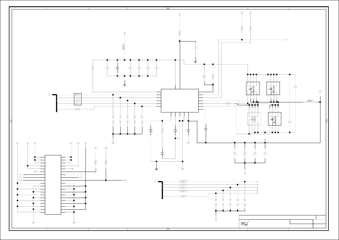
11-29-1999_14:46 30
VRM
JP16 JP27 JP28JP29 JP30
RP24
0K
1
2
3
45
6
7
8VID1[0]
VID1[1]
VID1[2]
VID1[3]
VID1[4]
VID1[4:0]
5
R104
0K
VID3_R
VID2_R
VID1_R
VID0_R
R398
0K
10K
R371
VRM_G2
VRM_G1
Q4
4123
8765
R71
5.1-5%
OUTEN
VRM_PWRGD 33
2200UF
C100
2
1
C93
2200UF
1
2
2200UF
C103
2
1
JP9JP10 JP7JP6 JP8
R65
20
1200UF
C87
2
1
C111
1200UF
1
2
1200UF
C107
2
1
R55
8.2K
R53
5.6K
R332
220
2.7K
R54
VRM_COMP
VRM_SS
VRM_IFB
VRM_FAULT
VRM_VFB
VRM_COMP_R
C82
1200UF
1
2
C366
2200UF
1
2
Q5
5678
3214
Q3
5678
3214
Q2
4123
8765
PVCC_R
C72
0.01UF
1
2
C90
0.1UF
C73
150PF
C75
0.1UF
C86
0.1UF
10UF
C140
2
1
C74
0.01UF
C71
1000PF
1UF-X7R
C118
2
1
1UF-X7R
C119
1
2
VR3
18
17
16
15
14
19
6
9
4
3
7
13
20
8
1
5
2
12
10
11
VRM_IMAX
ETQP6F0R8L
1.0UH-20A
L18
IFB_Q
VRM_VCC5
DO3316P-102
1UH
L19
1UF-X7R
C97
2
1
J14
B16A16
B1A1
B2
B3A3
A2
B20
B19
B18
B17
A20
A19
A18
A17
B4
B5
B6
B7
B8
B9
B10
B11
B12
A4
A5
A6
A7
A8
A9
A10
A11
A12
A13 B13
B14A14
B15A15
30 VID1_0R
30 VID1_2R
30 VID1_4R
30VID1_3R
33VRM1_PWRGD
R370
220
30VID1_1R
VID[4:0]
3VID0
VID1
VID2
VID3
VID4
10K
R80
RP21
0K
8
7
6
54
3
2
1
30VID1_0R
30VID1_1R
30VID1_2R
30VID1_3R
30VID1_4R
VID4_R
PCD PLATFORM DESIGN
REV:
DRAWN BY:
LAST REVISED:
PROJECT:
SHEET:
FOLSOM, CALIFORNIA 95630
1900 PRAIRIE CITY ROAD
87654321
A
B
C
D
12345678
D
C
B
A
TITLE: INTEL(R) 820 CHIPSET DUAL PROCESSOR CUSTOMER REFERENCE BOARD 3.03
OF 38
R
VCCVID1
VCC3_3VCC3_3
VCC12 VCC5 VCC5 VCC12
G1
S1
S2
S3
D1
D2
D3
D4
SI4410DY
VCC3_3
+
+
+
+
+
+
VCC5
VCC12
+
+
G1
S1
S2
S3
D1
D2
D3
D4
SI4410DY
G1
S1
S2
S3
D1
D2
D3
D4
SI4410DY
G1
S1
S2
S3
D1
D2
D3
D4
SI4410DY
+
+
+
+
LTC1753
SENSE
SS
SGND
GND
VCC
PVCC
COMP
VID4
VID3
VID2
VID1
VID0
OUTEN IMAX
PWRGD
FAULT#
G1
G2
IFB
VFB
+
VCCVID
VCCVID1
GND8V_OUT3
V5_IN3V5_IN0
V5_IN4
V5_IN5V5_IN2
V5_IN1
GND10
V_OUT10
GND9
V_OUT9
V_OUT5
GND4
V_OUT4
GND3
V12_IN1
OUT_EN
VID1
VID3
PWR_GOOD
GND5
V_OUT6
GND6
V12_IN0
V12_IN2
ISHARE
VID0
VID2
VID4
V_OUT0
GND0
V_OUT1
GND1 V_OUT7
GND7V_OUT2
V_OUT8GND2
VRM8_4
RSV
VCC5
VID Override Jumpers
Sanyo 4SP2200M
No Stuff C106
C118, C119 must be next to FETs.
C82,C87,C107,C111 must support >6A of RMS current.
Place caps next to output FETs.
VRM
VRM requirements are based on VRM8.4 spec .
VID Override Jumpers
Default JP6-JP10 OUT.
Remove RP21, R398 for VID override.
Default JP16, JP27-JP30 OUT.
Remove RP24, R104 for VID override.
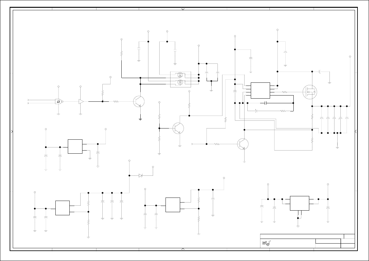
11-29-1999_14:46 31
VOLTAGE REGULATORS
Q18
MMBT3904LT1
B
C
E
R383
1K 1K
R382
100-1%
R133
100-1%
R134
301-1%
R311
131-1%
R309
R146
1.21K-1% 1%
R141
301
9,11,18,33 PWROK
R330
1K
1K
R340
R331
1K
11,33 SLP_S3#
VR8
3
2
1
U18
7
14 6
5
4
VR4
LT1585A-1_5
3
2
1
VD_G2VD_G1 VD_G3
VCC1_8_ADJ
VCC2_5_ADJ
VDDQ_FB
VDDQ_COMP_R
7.5K-1%
R137
VDDQ_G VDDQ_G2
U14
12
7
14
C347
47UF C324
47UF
1UF-X7R
C104
12
1UF-X7R
C268 21
100UF
C124 21
100UF
C142
12
100UF
C319
12
C159
100UF
21
100UF
C167
12
1UF-X7R
C35
12
C161
1UF-X7R
12
C91
100UF
21
C193
10UF
12
C174
1UF
21
47UF
C173
21
1UF-X7R
C200 21
C225
1UF-X7R
21
1UF-X7R
C211 12
C179
1UF-X7R
21
VR5
3
2
1
C160
220UF
21
VDDQ_COMP
330UF-T510
C15 21
LT1575
VR6
4
3
2
1
5
6
7
8
10PF
C164
C168
47UF
21
22UF
C242 12
VCC5DUAL_R
MMBT3904LT1
Q13
E
C
B
LT1529-3_3
VR1
6
24
51
3
Q6
1
2
3
1500UF
C352
21
1500UF
C33612
R135
5.1-5%
21 TYPEDET#
TYPEDET_R#
SI4562DY
Q12
8
5
2
4
1
3
7
6
100UF
C311 21
C368
100UF
12
100UF
C372 21
R379
10K
2.2K
R158
MMBT3904LT1
Q7
E
C
B
R381
1K
BAT17
CR11
A
C
PCD PLATFORM DESIGN
REV:
DRAWN BY:
LAST REVISED:
PROJECT:
SHEET:
FOLSOM, CALIFORNIA 95630
1900 PRAIRIE CITY ROAD
87654321
A
B
C
D
12345678
D
C
B
A
TITLE: INTEL(R) 820 CHIPSET DUAL PROCESSOR CUSTOMER REFERENCE BOARD 3.03
OF 38
R
VCC3_3
13
2
VCC1_8
VCC3_3SBY
VCC5
VCC5DUAL
VCC5
VTT1_5
VCC3_3
VCC3_3SBY
VCC3_3
VCC5DUAL
VCC12
VCC3_3
VCC12
VCC5SBY
VCC5SBY
VIN
VOUT
ADJ
LT1587ADJ
74LS132 VCC
GND
VCC5SBY
VIN
VOUT
GND
SN74LVC07A GND
VCC
VDDQ
+ +
+
+
+
+
+
+
+
+
+
+
+
+
+
+
+
VIN
VOUT
ADJ
LT1587ADJ
+
+
IPOS
INEG
GATE
COMP
SHDN
VIN
GND
FB
+
+
13
2
VIN VOUT
SHDN#
GND3
TAB
SENSE
IRL2203NS
1
3
2
+
+
D1
D2A
G1
G2
S1
S2
D1A
D2
+
+
+
VCC2_5
VCC1_8
13
2
VCC2_5SBY
-
+
It should be used only for further regulation of lower voltage power planes
The VCC5DUAL plane should not drive any logic components requiring 5V.
because the true voltage of VCC5DUAL will not remain constant
Rdson of the FET is not negligible for large currents
VTT 1.5 VOLTAGE REGULATOR
VCC3_3SBY VOLTAGE REGULATOR
AGP VDDQ VOLTAGE REGULATOR
VCC 5V DUAL VOLTAGE SWITCHER
VCC2_5 VOLTAGE REGULATOR
VCC 1.8 VOLTAGE REGULATOR
SN74LVC07A has 5V input and output tolerance.
Route VR6 GND to VDDQ output caps and then via to ground.
Voltage Regulators
Place C311 at regulator.
Place C108, C333 at RIMMs
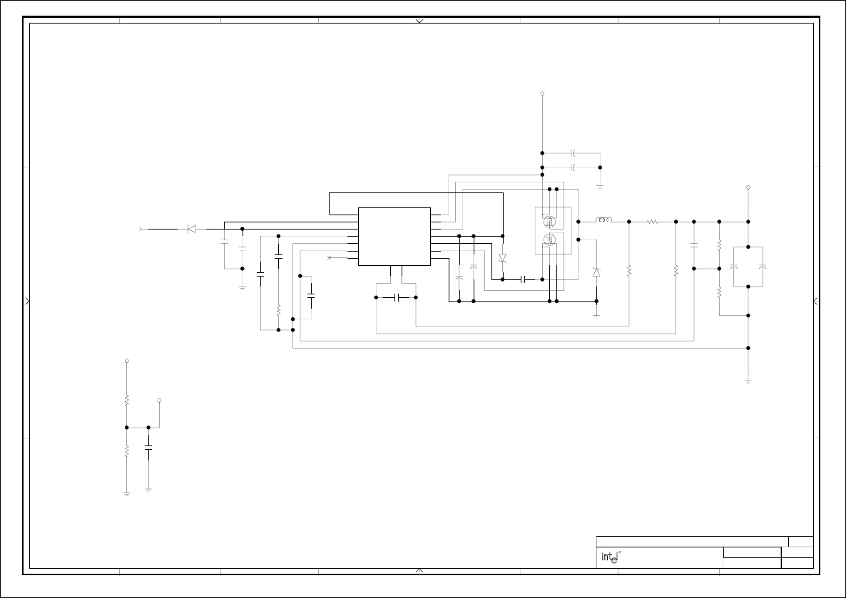
11-29-1999_14:46 32
VOLTAGE REGULATORS
SLP_S5#11
VCC2_5SBY_INTVCC
100-1%
R297
10K
R294
0.01
R325
R302
11K
CDRH125
10UH
L23
100-1%
R258
35.7-1%
R259
CMDSH-3
CR9
C
A
VCC2_5SBY_ITH
VCC2_5SBY_VOSENSE
VCC2_5SBY_SENSE-
VCC2_5SBY_SENSE+
VCC2_5SBY_L
VCC2_5SBY_TG
VCC2_5SBY_SW
VCC2_5SBY_BG
SBY_ITH_R
CR10
MBRS140T3
C
A
C295
68PF
1UF-X7R
C315
12
100-1%
R301
100PF
C304
C325
330UF
12
C326
330UF
21
100UF
C314
21
C312 0.1UF
V_BOOST
C306 4.7UF12
C299 1000PF
C292
100PF
100PF
C293
C263
0.1UF
C307 0.1UF
21
330PF
C296
VR7
8
7
6
10
11
15
12
14
16
13
5
3
2
1
4
9
VCC2_5SBY_COSC
VCC2_5SBY_RUN
C294
0.1UF
CR8
MMBD914LT1
31
10K
R295
Q11
31
57
42
68
PCD PLATFORM DESIGN
REV:
DRAWN BY:
LAST REVISED:
PROJECT:
SHEET:
FOLSOM, CALIFORNIA 95630
1900 PRAIRIE CITY ROAD
87654321
A
B
C
D
12345678
D
C
B
A
TITLE: INTEL(R) 820 CHIPSET DUAL PROCESSOR CUSTOMER REFERENCE BOARD 3.03
OF 38
R
VCC5DUAL
VCC2_5SBY
VCC2_5SBY
-
+
-
+
+
+
+
+
+
+
LT1435
RUN/SS
ITH
SGND
VIN
TG
SW
INTVCC
BOOST
BG
PGND
SENSE-
SENSE+
COSC
SFB
VOSENSE
EXTVCC
VCMOS1_8SBY
D1 D3
G1 G2
D2 D4
S1 S2
SI4966DY
TPS x2
AVX 330uF
VCC 2.5 Standby Voltage Regulator
VCMOS Generator For Rambus
Do not stuff C292.
Do not stuff C304.
Voltage Regulators
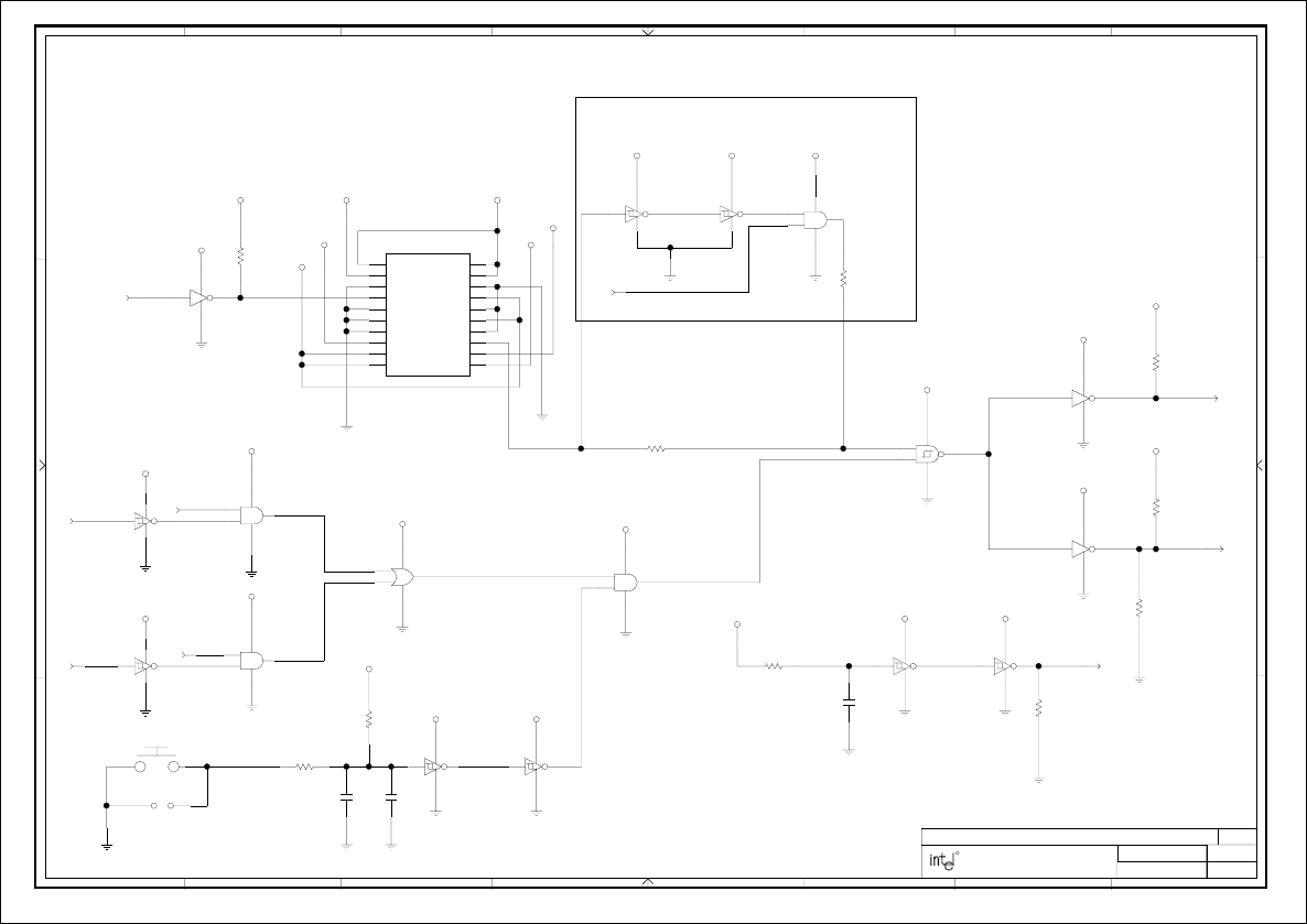
11-29-1999_14:46
POWER CONNECTOR
33
RSTBTN_SW
JP12
U26
SN74LVC08A
2
13
7
14
6
SLOTOCC1#
30 VRM1_PWRGD
U23 14
7
89
U23
56
7
14
U23 14
7
21
U23
34
7
14 RS_SCH
U20
7
14
3 4 9,11,18,31PWROK
0K
R339
R342
0K
1M
R288
R251
22K
11,31 SLP_S3#
R347
4.7K
SLP_S3
R343
22
PWRGOOD4,6
330
R96
1M
R348
ATX_PWOK
POK_U1 POK_U2 POK_U3
RSMRST# 11,19
RSMRSTRSMRST_U
ATX_PWOK_R
PWROK_INV
U15
34
7
14
U20 21 14
7
U15 14
7
65 U15
98
7
14
U20 65 14
7
4DBRESET#
10UF
C328C335
0.01UF
1UF
C266
U15 14
7
21
J24
11
12
13
14
15
16
17
18
19
20
1
2
3
4
5
6
7
8
9
10
U3
2
13
7
14
SW2
VRM_PWRGD30
U18
7
14 8
10
9
R349
4.7K
U9
SN74LVC08A
14
7
3
1
2
4SLOTOCC0#
U9
14
7
8
9
10
220K
R372
U22
2
13
7
14
PCD PLATFORM DESIGN
REV:
DRAWN BY:
LAST REVISED:
PROJECT:
SHEET:
FOLSOM, CALIFORNIA 95630
1900 PRAIRIE CITY ROAD
87654321
A
B
C
D
12345678
D
C
B
A
TITLE: INTEL(R) 820 CHIPSET DUAL PROCESSOR CUSTOMER REFERENCE BOARD 3.03
OF 38
R
VCC3_3SBY
VCC3_3SBY
74LVC14A
VCC3_3SBY
74LVC14A
VCC3_3SBY
VCC5SBY
74LVC14A74LVC14A
VCC3_3SBYVCC3_3SBY
VCC3_3SBY
VCC3_3SBY
VCC3_3SBY
SN74LVC06A GND
VCC
VCC3_3SBY
VCC3_3SBY VCC3_3SBY VCC3_3SBY
VCC5M
VCC12-
VCC12
VCC5
VCC5SBY
VCC3_3
VCC5SBY
VCC2_5
VCC5SBY
VCC3_3SBY
74LVC14A
SN74LVC06A GND
VCC
VCC3_3SBY
74LVC14A 74LVC14A
VCC3_3SBY
SN74LVC06A GND
VCC
74LVC14A
ATX
3_3V11
-12V
GND13
PS_0N
GND15
GND16
GND17
-5V
5V19
5V20
3_3V1
3_3V2
GND3
5V4
GND5
5V6
GND7
PW_OK
5VSB
12V
SN74LVC08A
74LS132 VCC
GND
SN74LVC08A
VCC3_3SBY
VCC3_3SBY
74LVC32
330 ohm pullup to VCC3_3 located on CPU sheet.
For test only
and Schmitt trigger logic.
using a 22 msec delay
Resume Reset circuitry
No stuff.
For test only
No stuff.
ATX Connector
74LVC14A has 5V input tolerance.
ITP Reset circuit. For debug only.
SN74LVC06A has 5V input tolerance.
SN74LVC06A has 5V output tolerance.
No stuff R342 when ITP is used.
Power Connector
Reset Button
220 ohm pullup to VCC3_3 is located on VRM sheet.
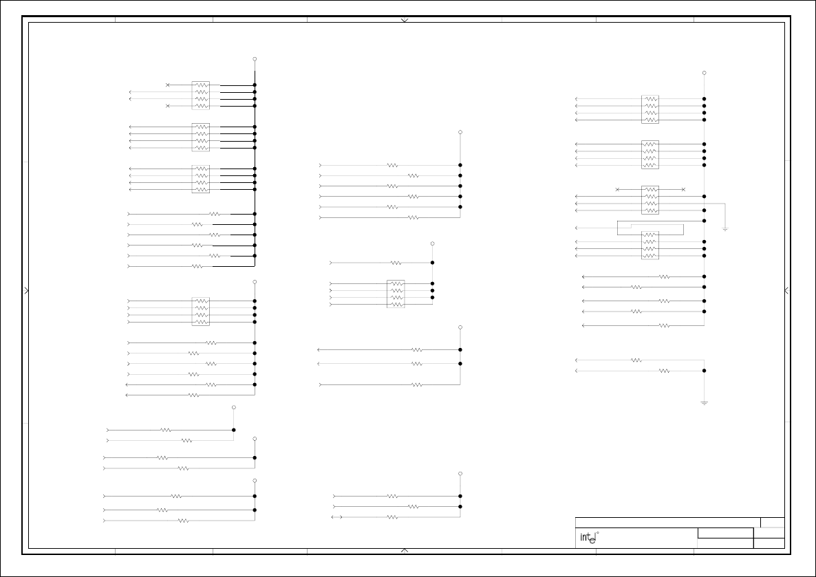
11-29-1999_14:46
PCI/AGP PULLUPS/PULLDOWNS
34
8.2K
R394
9,21 ST2
9,21 ST0
ST1
9,21 8.2K
R384
R385
8.2K
R393
100K
SBSTB#
9,21
9,21 SBSTB
9,21 GGNT#
WBF#
9,21
9,21 PIPE#
PIRQ#B
10,21,22,23
PIRQ#A
10,18,21,22,23
8.2K
R89
R81
8.2K
ALERTCLK_SBY
11,18 4.7K
R13
R12
4.7K
GNT#A
10,23
10,24 IRQ15
10,24 IRQ14
8.2K
R323
R338
8.2K
SMB_ALERT
11 4.7K
R236
R374
1K
1K
R85
SMBDATA_CORE
3,5,11,13
R237
4.7K
4.7K
R235
R314
8.2K
4,6,10,12 HINIT#
4,6,10 LINT1
4,6,10 LINT0
4,6,10 A20M#
PREQ#3
10,18
PREQ#1
10,22
10,22 PREQ#0
10,14 A20GATE
10,14 KBRST#
8.2K
R198
10,18,22,23 PERR#
10,18,22,23 SERR#
10,18,22,23 STOP#
PGNT#4
10
PGNT#3
10,18 PGNT#2
10,23
PGNT#1
10,22
10,22 PGNT#0
21 GPERR#
21 GSERR#
9,21 GSTOP#
9,21 GFRAME#
R124
150
9,21 GIRDY#
8.2K
R327
R132
8.2K
9,21 ADSTB1
RBF#
9,21
9,21 GPAR
9,21 ADSTB#0
8.2K
R207
R136
8.2K
ADSTB#1
9,21
4,6,10 IGNNE#
PICD0
4,6,10
4,6,10 FERR#
4,6,10 SMI#
4,6,10 STPCLK#
4,6 FLUSH#
PICD1
4,6,10
R324
8.2K
SERIRQ
10,14,23
TESTHI
4
SLP#
4,6,10
R127
100K
R84
1K
R373
1K
ADSTB0
9,21
REQ#A
10,23
ALERTDATA_SBY
11,18
1K
R123
1K
R126
9,21 GTRDY#
RP15
8.2K
1
2
3
45
6
7
8
9,21 GDEVSEL#
8.2K
RP9 1
2
3
45
6
7
8
RP14
8.2K
8
7
6
54
3
2
1
RP8
8.2K
1
2
3
45
6
7
8
RP7
1K
8
7
6
54
3
2
1
10,18,22,23 TRDY#
10,18,22,23 FRAME#
10,18,22,23 IRDY#
RP10
2.7K
1
2
3
45
6
7
8
10,22,23 PLOCK#
10,22,23 PIRQ#C
10,22,23 PIRQ#D
RP11
2.7K
8
7
6
54
3
2
1150
R128
2.7K
R112
10,23 PGNT#5
10,23 PREQ#5
PREQ#2
10,23
R111
2.7K
2.7K
R115
R216
2.7K R213
2.7K
R109
2.7K
10 PREQ#4
8.2K
RP16 1
2
3
45
6
7
8
8.2K
R214
R256
8.2K R114
8.2K
8.2K
R105
10,18,22,23 DEVSEL#
SMBCLK_CORE
3,5,11,13
RP6
2.7K
8
7
6
54
3
2
1
GREQ#
9,21
TESTHI1
6
PCD PLATFORM DESIGN
REV:
DRAWN BY:
LAST REVISED:
PROJECT:
SHEET:
FOLSOM, CALIFORNIA 95630
1900 PRAIRIE CITY ROAD
87654321
A
B
C
D
12345678
D
C
B
A
TITLE: INTEL(R) 820 CHIPSET DUAL PROCESSOR CUSTOMER REFERENCE BOARD 3.03
OF 38
R
VCC3_3
VCC5
VDDQ
VCC2_5
VCC2_5
VCC3_3
VCC2_5
VCC5
VCC3_3
VCC3_3SBY
AGP
PROCESSOR
PCI
PCI/AGP Pullups/Pulldowns

11-29-1999_14:46 35
RAMBUS TERMINATION
13
TERM_ROW[2:0]
TERM_ROW1
TERM_ROW0
TERM_ROW2
13
TERM_DQB[8:0] TERM_DQB0
TERM_DQB2
TERM_DQB3
TERM_DQB4
TERM_DQB5
TERM_DQB6
TERM_DQB7
TERM_DQB8
TERM_DQB1
13
TERM_COL[4:0]
TERM_COL3
TERM_COL2
TERM_COL0
TERM_COL1
TERM_COL4
13
TERM_DQA[8:0]
TERM_DQA8
TERM_DQA3
TERM_DQA2
TERM_DQA1
TERM_DQA6
TERM_DQA5
TERM_DQA4
TERM_DQA0
TERM_DQA7
13 TERM_SCK
TERM_CMD
13
C280
0.1UF C278
0.1UF
C281
0.1UF C282
0.1UF
0.1UF
C283
0.1UF
C273
0.1UF
C275
0.1UF
C274
0.1UF
C276
0.1UF
C279
0.1UF
C271
C269
0.1UF
C277
0.1UF
R277
28 R279
28 R278
28 R281
28
28 R280
28 R283
28 R282
28 R285
R284
28 R268
28 R267
28 R266
28
28 R265
28 R264
28 R263
28 R262
R261
28 R260
28 R275
28 R274
28
R276
28 R269
28
28 R271
28 R270
28 R273
28 R272
R292
39.2-1%
R290
39.2-1%
90.9-1% R293
90.9-1% R291
PCD PLATFORM DESIGN
REV:
DRAWN BY:
LAST REVISED:
PROJECT:
SHEET:
FOLSOM, CALIFORNIA 95630
1900 PRAIRIE CITY ROAD
87654321
A
B
C
D
12345678
D
C
B
A
TITLE: INTEL(R) 820 CHIPSET DUAL PROCESSOR CUSTOMER REFERENCE BOARD 3.03
OF 38
R
VCC1_8
VCC1_8
Rambus Termination
NOTE :
per two RSL signals.
Use one 0.1uF cap
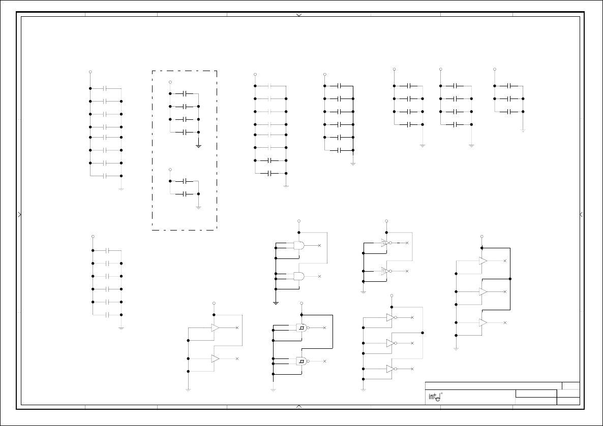
11-29-1999_14:44
DECOUPLING
36
0.1UF
C60 C29
0.1UF
0.1UF
C30
C157
0.1UF
0.1UF
C212C201
0.1UF
C166
0.1UF
C156
0.01UF
0.01UF
C213C202
0.01UF
C162
0.01UF
0.1UF
C253
0.1UF
C231C232
0.1UF
C248
0.1UF
C254
0.01UF
0.01UF
C224C230
0.01UF
C252
0.01UF
C222
0.1UF
0.1UF
C227
0.1UF
C229C258
0.1UF
0.1UF
C165
C210
100UF
100UF
C285C219
100UF
C288
100UF
100UF
C284C289
100UF
100UF
C303
100UF
C302
C226
0.1UF
0.1UF
C264C235
0.1UF
C255
0.1UF
C105
0.1UF
4.7UF
C88C290
4.7UF
U3
10
98
7
14
U3
14
7
11
12
13
U15 14
7
1011
U15
13 12
7
14
U20 89 14
7
U20
7
14
11 10
U20 1213 14
7
U14
14
7
98
U18
12
13 11
14
7
U14
1011
7
14
U19
43
7
14
U19
14
7
11 10
U19
1213
7
14
U18
7
14 3
2
1
C221
0.01UF
0.01UF
C270C272
0.01UF
0.01UF
C197C144
0.01UF
0.01UF
C143
PCD PLATFORM DESIGN
REV:
DRAWN BY:
LAST REVISED:
PROJECT:
SHEET:
FOLSOM, CALIFORNIA 95630
1900 PRAIRIE CITY ROAD
87654321
A
B
C
D
12345678
D
C
B
A
TITLE: INTEL(R) 820 CHIPSET DUAL PROCESSOR CUSTOMER REFERENCE BOARD 3.03
OF 38
R
VDDQ
VCC1_8
VCC5SBY
VCC3_3
VCMOS1_8SBYVCC2_5SBYVCC2_5SBY
SN74LVC08A
SN74LVC08A
74LVC14A
74LVC14A
VCC3_3SBY
SN74LVC06A GND
VCC
SN74LVC06A GND
VCC
SN74LVC06A GND
VCC
SN74LVC07A GND
VCC
74LS132 VCC
GND
VCC3_3SBY
SN74LVC07A GND
VCC
VCC3_3SBY
SN74LVC07A GND
VCC
SN74LVC07A GND
VCC
SN74LVC07A GND
VCC
74LS132 VCC
GND
VCC3_3SBY
VCC3_3SBYVCC3_3
VCC1_8
VDDQ
Place these caps on solder side
Place these caps on solder side
70 mils of outer balls of MCH.
Place VDDQ capacitors within
For chipset decoupling, use 0.1UF and
0.01UF decoupling capacitor at each
corner of the device. If there is room,
add 0.01UF capacitors in the middle
of each quad.
Place 100uF caps, 0.1 ohm ESR, among RIMM connectors.
Place a VCMOS1_8SBY 0.1uF cap at each RIMM.
Un-used Gates
RIMM Decoupling
82559 Decoupling.ICH Decoupling
MCH Decoupling
Decoupling
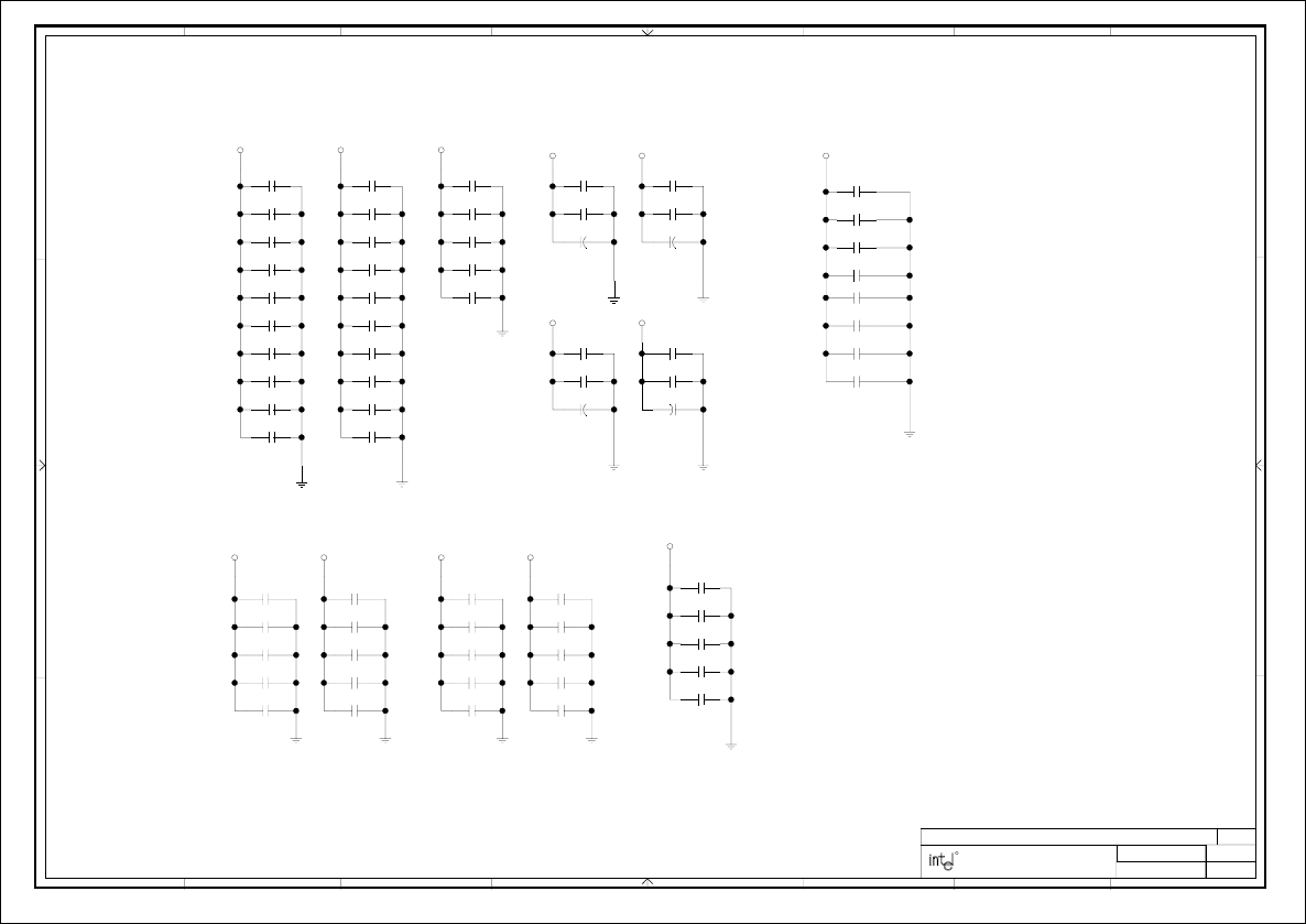
11-29-1999_14:44
BULK DECOUPLING
37
22UF
C367
21
10UF
C64
C65
10UF
C89
10UF
C106
10UF
10UF
C108 C114
10UF
10UF
C115
10UF
C125 C127
10UF
10UF
C128
0.01UF
C129
0.01UF
C130 C131
0.01UF
0.01UF
C132
0.1UF
C133
0.1UF
C134 C135
0.1UF
C136
0.1UF
22UF
C369
12
C370
22UF
21
22UF
C371
12
0.1UF
C137 C138
0.1UF
C139
0.1UF
C141
0.1UF
0.1UF
C145 C146
0.1UF
C147
0.1UF
0.1UF
C148
0.1UF
C149
0.1UF
C150 C151
0.1UF
0.1UF
C152 C153
0.1UF
0.1UF
C154 C163
0.1UF
0.1UF
C172 C175
0.1UF
0.1UF
C176
0.1UF
C177
0.1UF
C178 C181
0.1UF
0.1UF
C188 C195
0.1UF
0.1UF
C216 C238
0.1UF
0.1UF
C240 C259
0.1UF
0.1UF
C310
C330
0.1UF
C331
0.1UF
0.1UF
C332 C333
0.1UF
0.1UF
C334 C337
0.1UF
0.1UF
C338 C339
0.1UF
0.1UF
C340
0.1UF
C341
10UF
C342C343
10UF
10UF
C344
10UF
C345
C346
10UF
10UF
C351C357
10UF
C363
10UF
C364
10UF 10UF
C365
PCD PLATFORM DESIGN
REV:
DRAWN BY:
LAST REVISED:
PROJECT:
SHEET:
FOLSOM, CALIFORNIA 95630
1900 PRAIRIE CITY ROAD
87654321
A
B
C
D
12345678
D
C
B
A
TITLE: INTEL(R) 820 CHIPSET DUAL PROCESSOR CUSTOMER REFERENCE BOARD 3.03
OF 38
R
+
VCC3_3
++
+
VCC3_3VCC3_3 VCC5
VCC12-VCC12
VCCVID VCCVID
VTT1_5
VCC2_5
VCC3_3SBY
VCCVID1 VCCVID1
VCC2_5 DecouplingVCC3_3 DecouplingVCC3_3 Decoupling Termination Decoupling
Core Voltage Decoupling
Bulk Power Decoupling
Bulk Decoupling
Place caps at VTT pins on Slot 1 connector.
11-29-1999_14:44
REVISION HISTORY
38
PCD PLATFORM DESIGN
REV:
DRAWN BY:
LAST REVISED:
PROJECT:
SHEET:
FOLSOM, CALIFORNIA 95630
1900 PRAIRIE CITY ROAD
87654321
A
B
C
D
12345678
D
C
B
A
TITLE: INTEL(R) 820 CHIPSET DUAL PROCESSOR CUSTOMER REFERENCE BOARD 3.03
OF 38
R
Changed VDDQ cap values from 0.1uF to 0.01uF.
Deleted 3.3V decoupling for RIMM connectors. Added solder side decoup for MCH.
Changed value of capacitor C194 from 0.1uF to 0.01uF.
Modified MCH_AGPREF circuit, changed 432 ohm to 1K ohm and 62 ohm to 80.6 ohm.
Modified RIMM connectors to eliminate 3.3V, added 0.1uF decoup caps to SVDDA & SVDDB on each RIMM.
Revision History
Modified HUBREF circuit, deleted R222, R223 & C217, changed C218 from 470pF to 0.1uF.
Pg 8
Pg 10
Pg 13
Modified CMD and SCK termination values. Removed 470pF capacitors, Changed 93 ohm to 90.9 ohm,
and changed 39 ohm to 39.2 ohm resistors.
Pg 35
Pg 36

Intel around the world
United States and Canada
Intel Corporation
Robert Noyce Building
2200 Mission College Boulevard
P.O. Box 58119
Santa Clara, CA 95052-8119
USA
Phone: (800) 628-8686
Europe
Intel Corporation (UK) Ltd.
Pipers Way
Swindon
Wiltshire SN3 1RJ
UK
Phone:
England (44) 1793 403 000
Germany (49) 89 99143 0
France (33) 1 4571 7171
Italy (39) 2 575 441
Israel (972) 2 589 7111
Netherlands (31) 10 286 6111
Sweden (46) 8 705 5600
Asia-Pacific
Intel Semiconductor Ltd.
32/F Two Pacific Place
88 Queensway, Central
Hong Kong, SAR
Phone: (852) 2844 4555
Japan
Intel Kabushiki Kaisha
P.O. Box 115 Tsukuba-gakuen
5-6 Tokodai, Tsukuba-shi
Ibaraki-ken 305
Japan
Phone: (81) 298 47 8522
South America
Intel Semicondutores do Brazil
Rue Florida, 1703-2 and CJ22
CEP 04565-001 Sao Paulo-SP
Brazil
Phone: (55) 11 5505 2296
For more information
To learn more about Intel Corporation, visit our site
on the World Wide Web at www.intel.com
