Axell Wireless 55-165703 55-165703 Cell Enhancer User Manual 80 330501HBKM
Axell Wireless 55-165703 Cell Enhancer 80 330501HBKM
Contents
- 1. Manual 1 of 5
- 2. manual 2 of 5
- 3. manual 3 of 5
- 4. manual 4 of 5
- 5. manual 5 of 5
manual 3 of 5

STTRS DOCUMENTATION
Document Number 80-330501HBKM – Issue A - Draft Page 250 of 500
14.3.5. Attenuator 25W, 60dB (10-002960)
In many practical applications for Cell Enhancers etc., the gain in each path is found to be excessive.
Therefore, provision is made within the unit for the setting of attenuation in each path, to reduce the
gain. Attenuator 25W, 60dB (10-002960) is a fixed attenuator providing 60dB of signal attenuation.
10-002960 Specification
PARAMETER SPECIFICATION
Frequency Range DC to 2.5GHz
Power Handling 25 W
Attenuation 60 dB
Attenuation Accuracy ± 0.5dB
Return Loss to 2.2GHz 18dB
Nominal Impedance 50 Ω
RF Conectors N male to N female
Finish Matt Black Anodise
operational -20%C to +55%C
Temperature
range storage -20%C to +70%C

STTRS DOCUMENTATION
Document Number 80-330501HBKM – Issue A - Draft Page 251 of 500
15 ATTENUATOR SHELF (ITAC) 3 (55-165506)
Attenuator Shelf (ITAC) 3 (55-165506) list of major components
Section Component
Part Component Part Description Qty. Per
Assembly
15.3.1. 05-002602 900MHz Splitter/Combiner 1
15.3.2. 05-003007 4 Port Hybrid Coupler 1
15.3.3. 09-000902 Dummy load 1
15.3.4. 10-000901 Switched Attenuator 0.25W, 0 - 15dB 1
15.3.5. 10-002960 Attenuator 25W, 60dB 1
STTRS DOCUMENTATION
Document Number 80-330501HBKM – Issue A - Draft Page 252 of 500
15.1. Attenuator Shelf (ITAC) 3 (55-165506) outline drawing
Drawing number 55-1655106
STTRS DOCUMENTATION
Document Number 80-330501HBKM – Issue A - Draft Page 253 of 500
15.2 Attenuator Shelf (ITAC) 3 (55-165506) system diagram
Drawing number 55-165586
STTRS DOCUMENTATION
Document Number 80-330501HBKM – Issue A - Draft Page 254 of 500
15.3. Attenuator Shelf (ITAC) 3 (55-165506) major components
15.3.1. 900MHz Splitter/Combiner (05-002602)
The Splitter/Combiner used is a device for accurately matching two or more RF signals to single or
multiple ports, whilst maintaining an accurate 50Ω load to all inputs/outputs and ensuring that the
VSWR and insertion losses are kept to a minimum. Any unused ports should be terminated with an
appropriate 50Ω load.
Being passive devices, the splitters should have an extremely long operational life and require no
maintenance. Should a unit be suspect, it is usually most time efficient to replace the whole module
rather than attempt repair or re-tuning.
05-002602 Specification
PARAMETER SPECIFICATION
Narrowband 815 – 960MHz Frequency
range Broadband 800 – 1200MHz
Narrowband 145MHz
Bandwidth Broadband 400MHz
Input ports 1
Output ports 2
Narrowband 3.3dB
Insertion loss Broadband 3.5dB
Return loss input & output 1.3:1
Impedance 50Ω
Narrowband >20dB
Isolation Broadband >18dB
MTFB >180,000 hours
Splitting 20Watts
Power rating Combining 0.5Watt
Connectors SMA female
Weight 200g (approximately)
Size 54 x 44 x 21mm
15.3.2. 4 Port Hybrid Coupler (05-003007)
This transmitter hybrid coupler is a device for accurately matching two or more RF signals to single or
multiple ports, whilst maintaining an accurate 50Ω load to all inputs/outputs and ensuring that the
insertion losses are kept to a minimum. Any unused ports should be terminated with an appropriate
50Ω load. In this specific instance one port of 4 Port Hybrid Coupler (05-003007) is terminated with
Dummy load 09-000902 (see below).
05-003007 Specification
PARAMETER SPECIFICATION
Frequency range: 700-900MHz
Bandwidth: 200MHz
Rejection: >14dB
Insertion loss: 6.5dB (in band, typical)
Connectors: SMA
Weight: <1.0kg
operational
:-10%C to +60%C
Temperature
range: storage -20%C to +70%C
STTRS DOCUMENTATION
Document Number 80-330501HBKM – Issue A - Draft Page 255 of 500
15.3.3. Dummy Load (09-000902)
When a combiner system is used to split or combine RF signals, in many cases it is most cost
effective to use a standard stock item 4, 6 or 8 port device where, in fact, only a 3 or 6 port device is
needed. In this case 4 Port Hybrid Coupler (05-003007) has one of its ports terminated with Dummy
load (09-000902) in order to preserve the correct impedance of the device over the specified
frequency range.
09-000902 specification
PARAMETER SPECIFICATION
Frequency Range 0 - 2500 MHz
Power Rating 25 Watts continuous
VSWR Better than 1.1:1
Impedance 50 Ohms
Temperature Range -20 to +60°C
RF Connectors N Type female
Dimension 110.3mm x 38.1mm x
Weight 485 grams
Finish Black Anodised
RF Connector N Type male
Environmental IP66
MTBF >180,000 hours
15.3.4. Switched Attenuator 0.25W, 0 - 15dB (10-000901)
In many practical applications for Cell Enhancers etc., the gain in each path is found to be excessive.
Therefore, provision is made within the unit for the setting of attenuation in each path, to reduce the
gain.
10-000901 provides attenuation from 0 - 15dB in 2 dB steps The attenuation is simply set using the
four miniature toggle switches on the top of each unit. Each switch is clearly marked with the
attenuation it provides, and the total attenuation in line is the sum of the values switched in. They are
designed to maintain an accurate 50Ω impedance over their operating frequency at both input and
output.
10-000901 Specification
PARAMETER SPECIFICATION
Attenuation Values 0-15dB
Attenuation Steps 1, 2, 4 and 8dB
Power Handling 0.25 Watt
Attenuation Accuracy ± 1.0 dB
Frequency Range DC to 1GHz
Impedance 50Ω
Connectors SMA
VSWR 1.3:1
Weight 0.2kg
operation -20°C to +60°C Temperature
range storage -40°C to +70°C
STTRS DOCUMENTATION
Document Number 80-330501HBKM – Issue A - Draft Page 256 of 500
15.3.5. Attenuator 25W, 60dB (10-002960)
In many practical applications for Cell Enhancers etc., the gain in each path is found to be excessive.
Therefore, provision is made within the unit for the setting of attenuation in each path, to reduce the
gain. Attenuator 25W, 60dB (10-002960) is a fixed attenuator providing 60dB of signal attenuation.
10-002960 Specification
PARAMETER SPECIFICATION
Frequency Range DC to 2.5GHz
Power Handling 25 W
Attenuation 60 dB
Attenuation Accuracy ± 0.5dB
Return Loss to 2.2GHz 18dB
Nominal Impedance 50 Ω
RF Conectors N male to N female
Finish Matt Black Anodise
operational -20%C to +55%C
Temperature
range storage -20%C to +70%C

STTRS DOCUMENTATION
Document Number 80-330501HBKM – Issue A - Draft Page 257 of 500
16. CONVENTION PLACE STATION LINE AMPLIFIER (80-330556)
C01-CR-05
Description of Convention Place Station Line Amp. (80-330556)
From the top of the rack
55-165709
55-165703
55-165704
Convention Place Station Line Amp. (80-330556) list of major components
Section Component
Part Component Part Description Qty. Per
Assembly
16.3.1. 55-165703 800MHz Line Amplifier 1
16.3.2. 55-165704 700MHz LINE AMP + FILTERS (INT AMP) 1
16.3.3. 55-165709 Convention Place Station Splitter 1
STTRS DOCUMENTATION
Document Number 80-330501HBKM – Issue A - Draft Page 258 of 500
16.1. Convention Place Station Line Amp. (80-330556) Rack elevation
Drawing number 80-330556
STTRS DOCUMENTATION
Document Number 80-330501HBKM – Issue A - Draft Page 259 of 500
16.2. Convention Place Station Line Amp. (80-330556) System diagram
Drawing number 80-330586
STTRS DOCUMENTATION
Document Number 80-330501HBKM – Issue A - Draft Page 260 of 500
16.3. Convention Place Station Line Amp. (80-330556) Alarm wiring diagram
Drawing number 80-330526

STTRS DOCUMENTATION
Document Number 80-330501HBKM – Issue A - Draft Page 261 of 500
16.4 Convention Place Station Line Amp. (80-330556) Sub Components
16.4.1. 800MHz Line Amplifier (55-165703)
800MHz Line Amplifier (55-165703) List of Major Components
800MHz Line Amplifier (55-165703) List of Major Components
Section Component
Part Component Part Description Qty. Per
Assembly
16.4.1.3. 02-007206 Bandpass Filter 4
16.4.1.4. 07-015105 Wideband Asymmetric Coupler 1
16.4.1.5. 10-000901 Switched Attenuator 0.25W, 0 - 15dB 2
16.4.1.6. 11-006702 Low Noise Amplifier 1
16.4.1.7. 12-018002 Power Amplifier (20W 800MHz ) 1
16.4.1.8. 12-021901 Low Power Amplifier 2
17-001109* AGC Detector Assembly (Logarithmic) 1
17-001117* AGC Detector Assembly 1
16.4.1.9.
17-001201* AGC Attenuator Assembly 2
16.4.1.10. 20-001601 12V (Dual) Relay Board 1
16.4.1.11. 80-008901 12V (Single) Relay Board 1
16.4.1.12. 94-100004 Dual Diode Assembly 1
16.4.1.13. 96-200047 DC/DC Converter 1
16.4.1.14. 96-300052 12V Switch-Mode PSU 1
*The sub components 17-001109, 17-001117 & 17-001201 are parts of the Automatic Gain Control
(AGC) system used in 800MHz Line Amplifier (55-165703); 17-001117 and 17-001201 are paired for
use in the uplink and 17-001109 and 17-001201 are paired for use in the downlink
STTRS DOCUMENTATION
Document Number 80-330501HBKM – Issue A - Draft Page 262 of 500
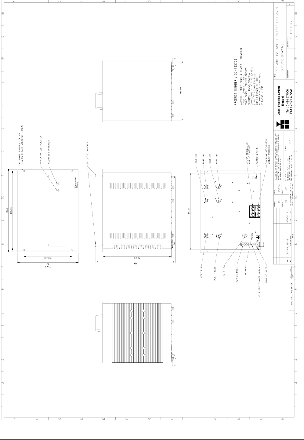
16.4.1.1. 800MHz Line Amplifier (55-165703) Outline Drawing
Drawing number 55-1657103
STTRS DOCUMENTATION
Document Number 80-330501HBKM – Issue A - Draft Page 263 of 500
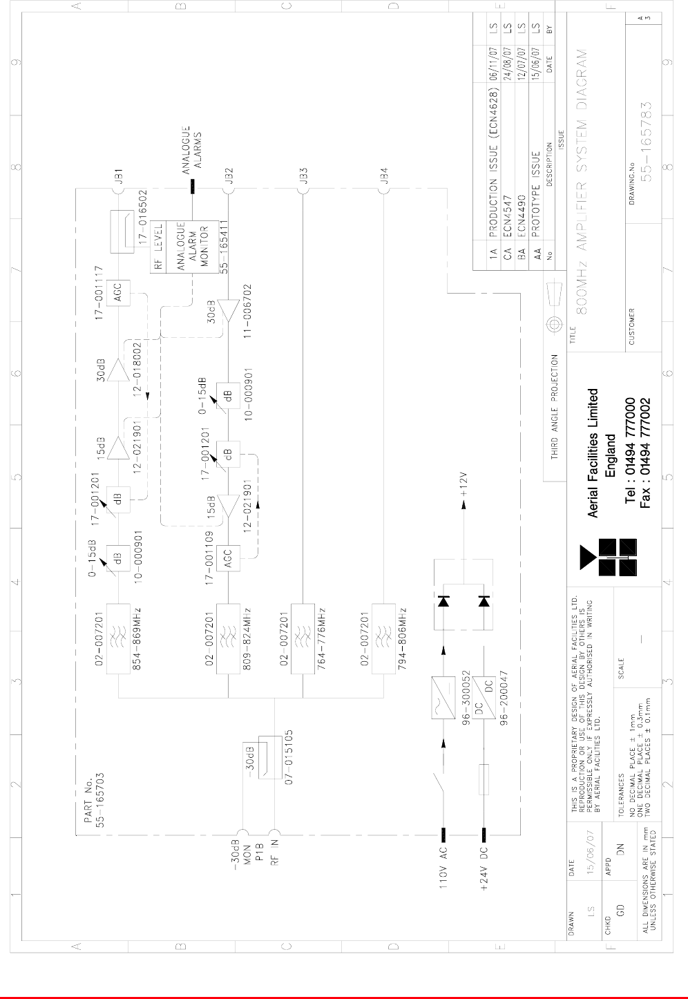
16.4.1.2. 800MHz Line Amplifier (55-165703) System Diagram
Drawing number 55-165783

STTRS DOCUMENTATION
Document Number 80-330501HBKM – Issue A - Draft Page 264 of 500
16.4.1.3. Bandpass Filter (02-007206)
The bandpass filters are multi-section designs with a bandwidth dependent upon the passband
frequencies, (both tuned to customer requirements). The response shape is basically Chebyshev with
a passband design ripple of 0.1dB. The filters are of slot coupled, folded combline design, and are
carefully aligned during manufacture in order to optimise the insertion loss, VSWR and
intermodulation characteristics of the unit. The tuned elements are silver-plated to reduce surface
ohmic losses and maintain a good VSWR figure and 50Ω load at the input and output ports.
Being passive devices, the bandpass filters should have an extremely long operational life and require
no maintenance. Should a filter be suspect, it is usually most time efficient to replace the module
rather than attempt repair or re-tuning.
No adjustments should be attempted without full network sweep analysis facilities to monitor both
insertion loss and VSWR simultaneously.
02-007206 Specification
PARAMETER SPECIFICATION
Response type Chebyshev
Frequency range 800 - 950MHz *
Bandwidth 25MHz *
Number of sections 8
Insertion loss 1.2 dB
VSWR better than 1.2:1
Connectors SMA female
Power handling 100W max
operation -20°C to +60°C Temperature
range storage -40°C to +70°C
Weight 3 kg (typical) *tuned to Customer's specification
16.4.1.4. Wideband Asymmetric Coupler (07-015105)
The purpose of Wideband Asymmetric Coupler (07-015105) is to tap off a known portion (in this case
30dB) of RF signal from transmission lines and to combine them, for example through splitter units for
different purposes (alarms/monitoring etc.), whilst maintaining an accurate 50Ω load to all
ports/interfaces throughout the specified frequency range. They are known formally as directional
couplers as they couple power from the RF mainline in one direction only.
07-015105 Specification
PARAMETER SPECIFICATION
Construction Inductive air gap
Frequency 800-2500MHz
Through loss 0.4dB (typical)
Coupling level -30dB ±0.5dB
Isolation N/A
Weight <1.0kg
Connectors SMA, female
operation -20°C to +60°C
Temperature
range storage -40°C to +70°C

STTRS DOCUMENTATION
Document Number 80-330501HBKM – Issue A - Draft Page 265 of 500
16.4.1.5. Switched Attenuator 0.25W, 0 - 15dB (10-000901)
In many practical applications for Cell Enhancers etc., the gain in each path is found to be excessive.
Therefore, provision is made within the unit for the setting of attenuation in each path, to reduce the
gain.
10-000901 provides attenuation from 0 - 15dB in 2 dB steps The attenuation is simply set using the
four miniature toggle switches on the top of each unit. Each switch is clearly marked with the
attenuation it provides, and the total attenuation in line is the sum of the values switched in. They are
designed to maintain an accurate 50Ω impedance over their operating frequency at both input and
output.
10-000901 Specification
PARAMETER SPECIFICATION
Attenuation Values 0-15dB
Attenuation Steps 1, 2, 4 and 8dB
Power Handling 0.25 Watt
Attenuation Accuracy ± 1.0 dB
Frequency Range DC to 1GHz
Impedance 50Ω
Connectors SMA
VSWR 1.3:1
Weigh 0.2kg
operation -20°C to +60°C Temperature
range storage -40°C to +70°C
16.4.1.6. Low Noise Amplifier (11-006702)
The Gallium-Arsenide low noise amplifiers used in 800MHz Line Amplifier (55-165703) are double
stage, solid-state low noise amplifiers. Class A circuitry is used throughout the units to ensure
excellent linearity and extremely low noise over a very wide dynamic range. The active devices are
very moderately rated to provide a long trouble-free working life. There are no adjustments on these
amplifiers, and in the unlikely event of a failure, then the complete amplifier should be replaced. This
amplifier features its own in-built alarm system which gives a volt-free relay contact type alarm that is
easily integrated into the main alarm system.
11-006702 Specification
PARAMETER SPECIFICATION
Frequency range: 800 – 1000MHz
Bandwidth: <200MHz
Gain: 29dB (typical)
1dB Compression point: 20dBm
OIP3: 33dBm
Input/Output return loss: >18dB
Noise figure: 1.3dB (typical)
Power consumption: 180mA @ 24V DC
Supply voltage: 10-24V DC
Connectors: SMA female
operational: -10°C to +60°C
Temperature range: storage: -20°C to +70°C
Size: 90 x 55 x 30.2mm
Weight: 290gms (approximately)

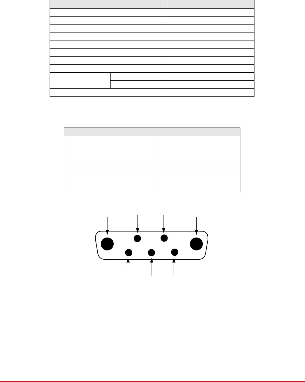
STTRS DOCUMENTATION
Document Number 80-330501HBKM – Issue A - Draft Page 266 of 500
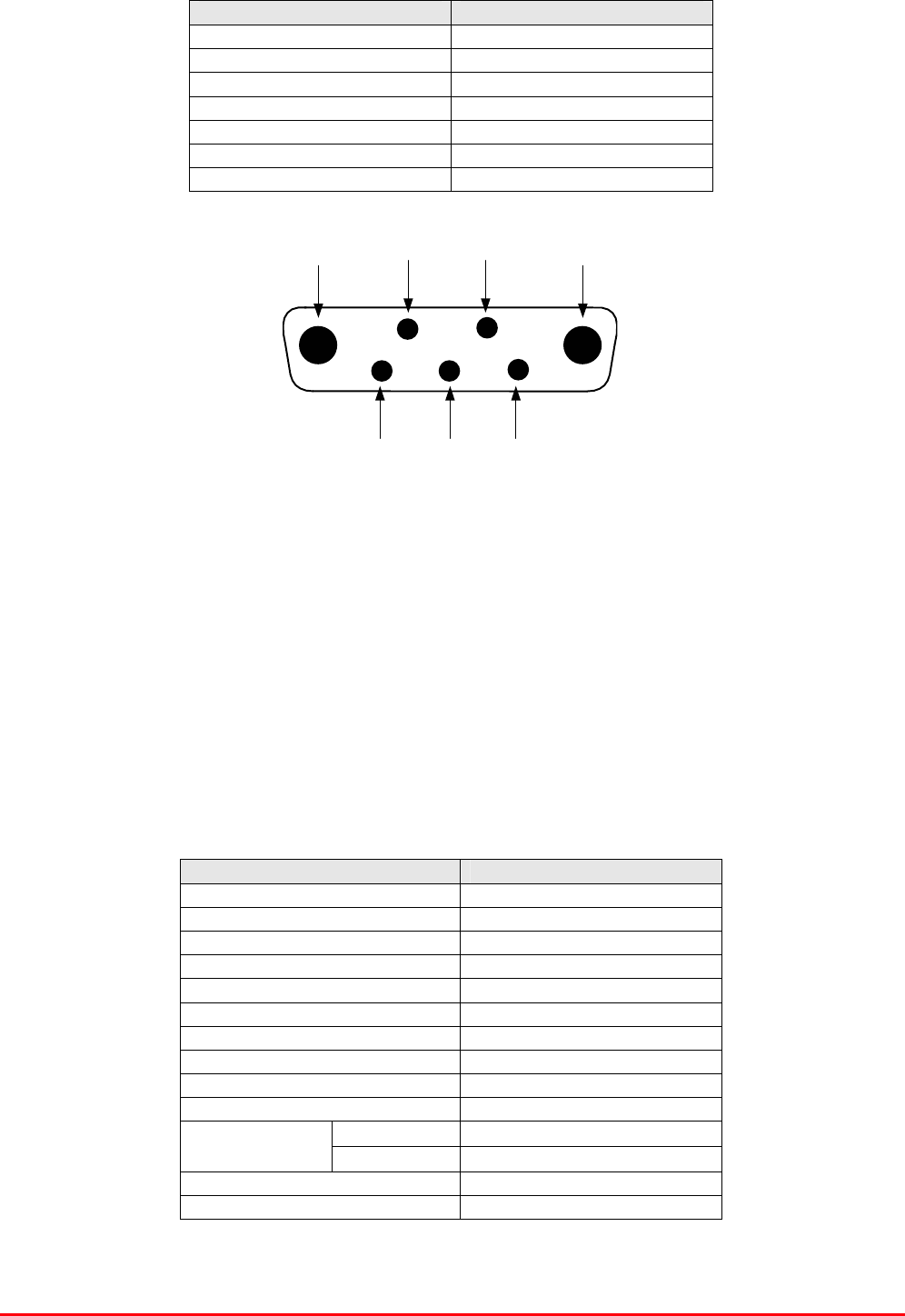
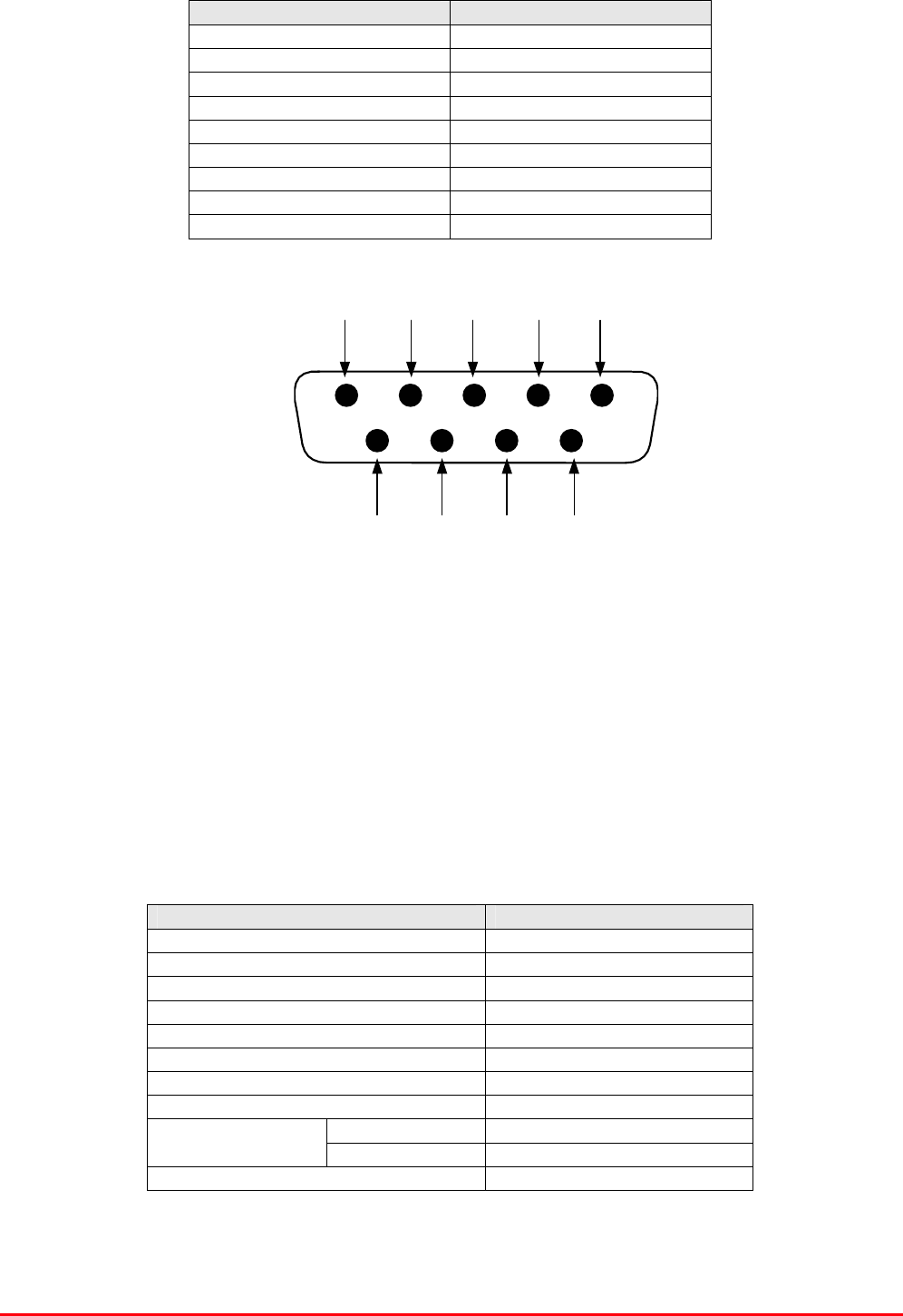
7 8 96
1 2 3 4 5
9-Way Pin-Out Graphical Representation
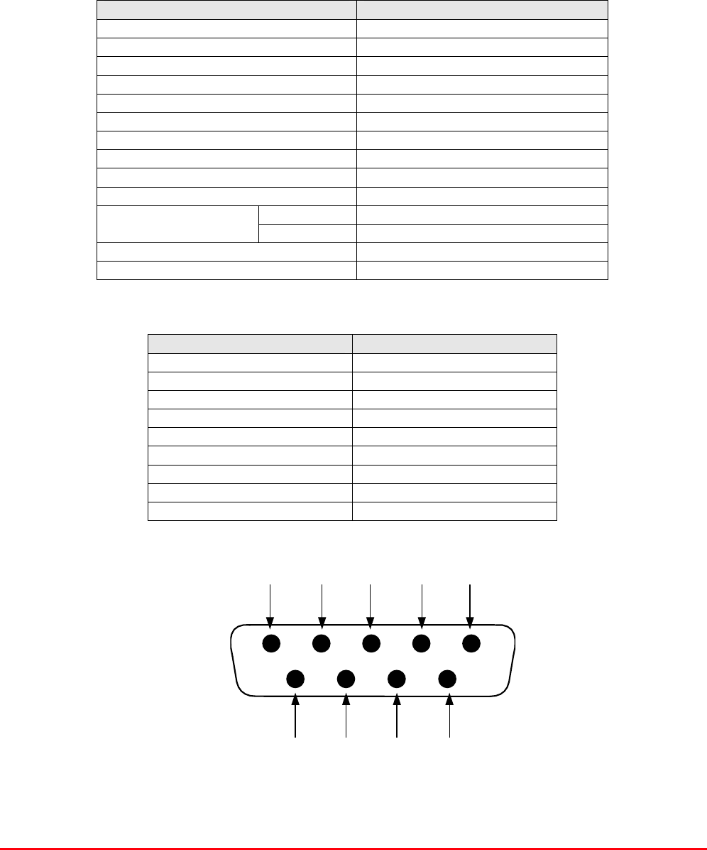
Low Noise Amplifier (11-006702) ‘D’ Connector Pin-out details
Connector pin Signal
1 +Ve input (10-24V)
2 GND
3 Alarm RelayO/P bad
4 Alarm Relay common
5 Alarm Relay good
6 No connection
7 TTL voltage set
8 TTL alarm/0V (good)
9 O/C good/0V bad
16.4.1.7. Power Amplifier (12-018002)
This amplifier is a Class A 20W power amplifier from 800-960MHz in a 1 stage balanced
configuration. It demonstrates a very high linearity and a very good input/output return loss (RL). It
has built in a Current Fault Alarm Function.
Its housing is an aluminium case (Iridite NCP finish) with SMA connectors for the RF input/output and
a D-Type connector for the power supply and the Current Fault Alarm Function.
12-018002 Specification
PARAMETER SPECIFICATION
Frequency range: 800-960MHz
Small signal gain: 30dB
Gain flatness: ±1.2dB
I/O Return loss: >18dB
1dB compression point: 42.8dBm
OIP3: 56dBm
Supply voltage: 24V DC
Supply current: 5.0Amps (Typical)
operational: -10°C to +60°C Temperature
range storage: -20°C to +70°C
Weight: <2kg (no heatsink)
STTRS DOCUMENTATION
Document Number 80-330501HBKM – Issue A - Draft Page 267 of 500
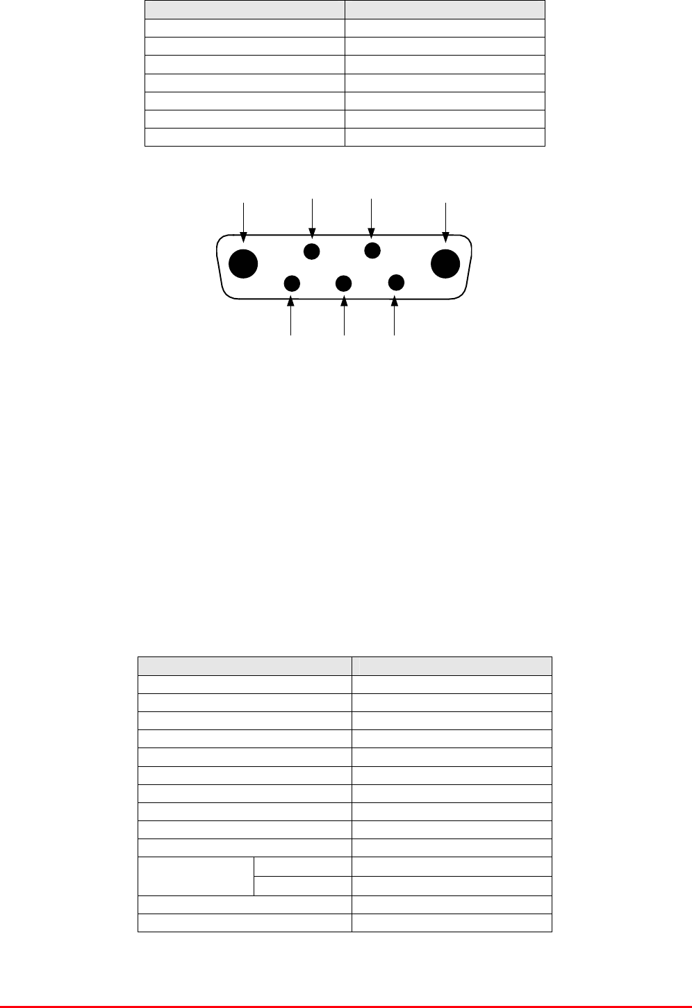
Power Amplifier (12-018002) 7-Way Connector Pin-outs
Connector Pin Signal
A1 (large pin) +24V DC
A2 (large pin) GND
1 Alarm relay common
2 TTL alarm/0V good
3 Alarm relay contact (bad)
4 Alarm relay contact (good)
5 O/C good/0V bad (TTL)
16.4.1.8. Low Power Amplifier (12-021901)
The low power amplifier used is a triple stage solid-state low-noise amplifier. Class A circuitry is used
in the unit to ensure excellent linearity over a very wide dynamic range. The three active devices are
very moderately rated to provide a long trouble-free working life.
Its housing is an aluminium case (Iridite NCP finish) with SMA connectors for the RF input/output and
a D-Type connector for the power supply and the Current Fault Alarm Function.
There are no adjustments on this amplifier, and in the unlikely event of failure then the entire amplifier
should be replaced.
Low Power Amplifier (12-021901) Specification
PARAMETER SPECIFICATION
Frequency range 800-960MHz*
Bandwidth 20MHz *
Maximum RF output >1.0 Watt
Gain 15dB
1dB compression point +30.5dBm
3rd order intercept point +43dBm
Noise Figure <6dB
VSWR better than 1.5:1
Connectors SMA female
Supply 500mA @ 10-15V DC
operational -10°C to +60°C
Temperature
range storage -20°C to +70°C
Weight 0.5 kg
Size 167x52x25mm
* Tuned to Customer’s specification

STTRS DOCUMENTATION
Document Number 80-330501HBKM – Issue A - Draft Page 268 of 500
Low Power Amplifier (12-021901) 7-Way Connector Pin-outs
Connector Pin Signal
A1 (large pin) +24V DC
A2 (large pin) GND
1 Alarm relay common
2 TTL alarm/0V good
3 Alarm relay contact (bad)
4 Alarm relay contact (good)
5 O/C good/0V bad (TTL)
16.4.1.9. Automatic Gain Control
17-001109 AGC Detector Assembly (Logarithmic)
17-001117 AGC Detector Assembly
17-001201 AGC Attenuator Assembly
The sub components 17-001109, 17-001117 & 17-001201 are parts of the Automatic Gain Control
(AGC) system used in 800MHz Line Amplifier (55-165703); 17-001117 and 17-001201 are paired for
use in the uplink and 17-001109 and 17-001201 are paired for use in the downlink
800MHz Line Amplifier (55-165703) is fitted with two differing types of Automatic Gain Control (AGC)
system, one linear, and one logarithmic. The AGC with logarithmic detector (17-001117) is fitted in the
uplink path and the AGC with linear detector (17-001109) is fitted in the downlink path
The AFL Automatic Gain Control system consists of two units, a detector/amplifier and an attenuator.
The detector/amplifier unit is inserted in the RF path on the output of the power amplifier, and the
attenuator is situated in the RF path between the 1st and 2nd stages of amplification.
17-001117 and 17-001201 are paired for use in the uplink and 17-001109 and 17-001201 are paired
for use in the downlink
The attenuator comprises a 50Ω P.I.N diode, voltage-variable attenuator with a range of 3 to 30dB.
The attenuation is controlled by a DC voltage which is derived from the associated detector controller
board.
Normally the attenuator is at minimum attenuation. The detector/amplifier unit monitors the RF level
being delivered by the power amplifier, and when a certain threshold is reached it begins to increase
the value of the attenuator to limit the RF output to the (factory set) threshold. Therefore overloading
of the power amplifier is avoided.
The factory set threshold is 1dB below the Enhancer 1dB compression point. Some adjustment of this
AGC threshold level is possible, a 10dB range is mostly achieved. It is not recommended under any
circumstances to adjust the AGC threshold to a level greater than the 1dB compression point as
system degradation will occur.
STTRS DOCUMENTATION
Document Number 80-330501HBKM – Issue A - Draft Page 269 of 500
The detector comprises of a 50Ω transmission line with a resistive tap which samples a small portion
of the mainline power. The sampled signal is amplified and fed to a conventional half wave diode
rectifier, the output of which is a DC voltage proportional to the RF input signal.
This DC voltage is passed via an inverting DC amplifier with integrating characteristics, to the output,
which drives the attenuation control line of the corresponding AGC attenuator. This unit is fitted at
some earlier point in the RF circuit.
For small signals, below AGC onset, the output control line will be close to 12V and the AGC
attenuator will have minimum attenuation. As the signal level increases the control line voltage will
fall, increasing the attenuator value and keeping the system output level at a constant value.
AGC Specification (both types)
PARAMETER SPECIFICATION
Frequency range up to 1000MHz
Attenuation range 3 to 30dB
Attenuation steps continuously variable
VSWR better than 1.2:1
RF Connectors SMA female
attenuator 1W Power
handling detector/amp >30W (or as required)
operation -10°C to +60°C Temperature
range storage -20°C to +70°C
attenuator pcb 50 x 42 x 21mm
Size detector/amp pcb 54 x 42 x 21mm
attenuator 90grams
Weight detector/amp 100grams
16.4.1.10. 12V (Dual) Relay Board (20-001601)
The General Purpose Relay Board allows the inversion of signals and the isolation of circuits. It is
equipped with two dual pole change-over relays with completely isolated wiring, accessed via screw
terminals. Both relays are provided with polarity protection diodes and diodes for suppressing the
transients caused by "flywheel effect" which can destroy switching transistors or induce spikes on
neighbouring circuits. It’s common use is to amalgamate all the alarm signals into one, volts-free relay
contact pair for the main alarm system.
20-001601 Specification
PARAMETER SPECIFICATION
Operating voltage: 8 to 30V (floating earth)
Alarm threshold: Vcc - 1.20 volt +15%
Alarm output relay contacts:
Max. switch current: 1.0Amp
Max. switch volts: 120Vdc/60VA
Max. switch power: 24W/60VA
Min. switch load: 10.0µA/10.0mV
Relay isolation: 1.5kV
Mechanical life: >2x10⁷ operations
Relay approval: BT type 56
Connector details: Screw terminals
operational: -10°C to +60°C Temperature
range storage: -20°C to +70°C
STTRS DOCUMENTATION
Document Number 80-330501HBKM – Issue A - Draft Page 270 of 500
16.4.1.11. 12V (Single) Relay Board (80-008901)
The General Purpose Relay Board allows the inversion of signals and the isolation of circuits. It is
equipped with a single dual pole change-over relay RL1, with completely isolated wiring, accessed
via a 15 way in-line connector.
The relay is provided with polarity protection diodes and diodes for suppressing the transients caused
by "flywheel effect" which can destroy switching transistors or induce spikes on neighbouring circuits.
It’s common use is to amalgamate all the alarm signals into one, volts-free relay contact pair for the
main alarm system.
80-008901 Specification
PARAMETER SPECIFICATION
Operating voltage 8 to 30V (floating earth)
Alarm threshold Vcc - 1.20 volt +15%
Alarm output relay contacts:
Max. switch current 1.0Amp
Max. switch volts 120Vdc/60VA
Max. switch power 24W/60VA
Min. switch load 10.0µA/10.0mV
Relay isolation 1.5kV
Mechanical life >2x10⁷ operations
Relay approval BT type 56
Connector details Screw terminals
operational -10°C to +60°C Temperature
range storage -20°C to +70°C
16.4.1.12. Dual Diode Assembly (94-100004)
The purpose of these dual diode assemblies is to allow two DC voltage sources to be combined, so
that the main DC rail within the equipment can be sourced from either a mains driven PSU, or
externally through an XLR connector or from dual mains driven PSUs . They are very heavy-duty
diodes and they prevent any reverse current from flowing back to their source or the alternative
supply rail. Combining diodes such as these will also be used if the equipment is to be powered from
external back-up batteries.
STTRS DOCUMENTATION
Document Number 80-330501HBKM – Issue A - Draft Page 271 of 500
16.4.1.13. DC/DC Converter 96-200047
96-200047 is an O.E.M. high power device with a wide input range and 12.5 amp @ 12V (150Watts)
output capability used to derive a 12V fixed voltage power supply rail from a higher voltage supply, in
this case 12V. In the event of failure this unit should not be repaired, only replaced.
96-200047 Specification
PARAMETER SPECIFICATION
DC Input Voltage range 19 to 36V
DC Output voltage 12V ± 1%
Max. current load 12.5Amps
Operation -10°C to +60°C Temperature
range Storage -20°C to +85°C
Working Humidity 20 to 90% RHNC
16.4.1.14. 12V Switch-Mode PSU (96-300052)
No routine maintenance of the PSU is required. If a fault is suspected, then the output voltage from
the power supply may be measured on its output terminals. This is typically set to 12.2V. The
adjustment potentiometer will be found close to the DC output terminals.
All the PSUs used in AFL Cell Enhancers are capable of operation from either 110 or 220V nominal
AC supplies. The line voltage is sensed automatically, so no adjustment or link setting is needed by
the operator.
96-300052 Specification
AC Input Supply 110 or 220V nominal
Voltage 85 - 265V AC
(absolute limits)
Frequency 47 to 63Hz
DC Output Supply 12V DC (nominal)
Voltage 10.5-13.8V (absolute limits)
Current 12.5A

STTRS DOCUMENTATION
Document Number 80-330501HBKM – Issue A - Draft Page 272 of 500
16.4.2 700MHz Line Amplifier (55-165704)
Description of 700MHz Line Amplifier (55-165704)
700MHz Line Amplifier (55-165704) List of Major Components
Section Component
Part Component Part Description Qty. Per
Assembly
16.4.2.3. 02-007206 Bandpass Filter 4
16.4.2.4. 07-015105 Wideband Asymmetric Coupler 1
16.4.2.5. 10-000901 Switched Attenuator 0.25W, 0 - 15dB 2
16.4.2.6. 11-006702 Low Noise Amplifier 1
16.4.2.7. 12-018002 Power Amplifier (20W 800MHz ) 1
16.4.2.8. 12-021901 Low Power Amplifier 2
17-001109* AGC Detector Assembly (Logarithmic) 1
17-001117* AGC Detector Assembly 1
16.4.2.9.
17-001201* AGC Attenuator Assembly 2
16.4.2.10. 80-008901 12V (Single) Relay Board 1
16.4.2.11. 94-100004 Dual Diode Assembly 1
16.4.2.12. 96-200047 DC/DC Converter 1
16.4.2.13. 96-300052 12V Switch-Mode PSU 1
*The sub components 17-001109, 17-001117 & 17-001201 are parts of the Automatic Gain Control
(AGC) system used in 800MHz Line Amplifier (55-165703); 17-001117 and 17-001201 are paired for
use in the uplink and 17-001109 and 17-001201 are paired for use in the downlink
STTRS DOCUMENTATION
Document Number 80-330501HBKM – Issue A - Draft Page 273 of 500
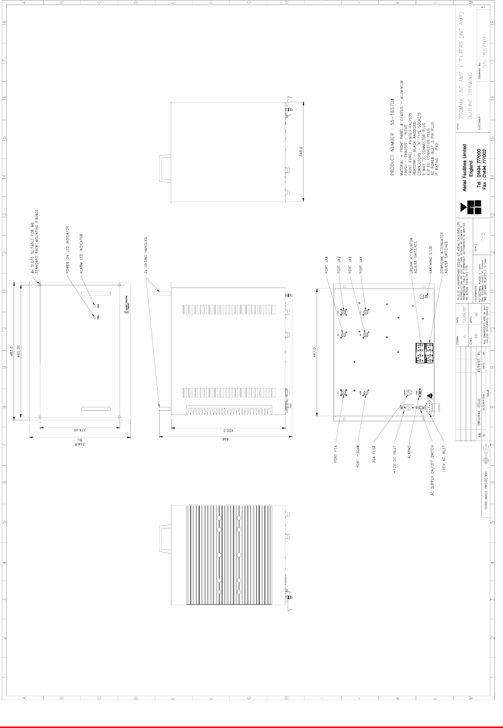
16.4.2.1. 700MHz Line Amplifier (55-165704) Outline Drawing
Drawing number 55-1657104
STTRS DOCUMENTATION
Document Number 80-330501HBKM – Issue A - Draft Page 274 of 500
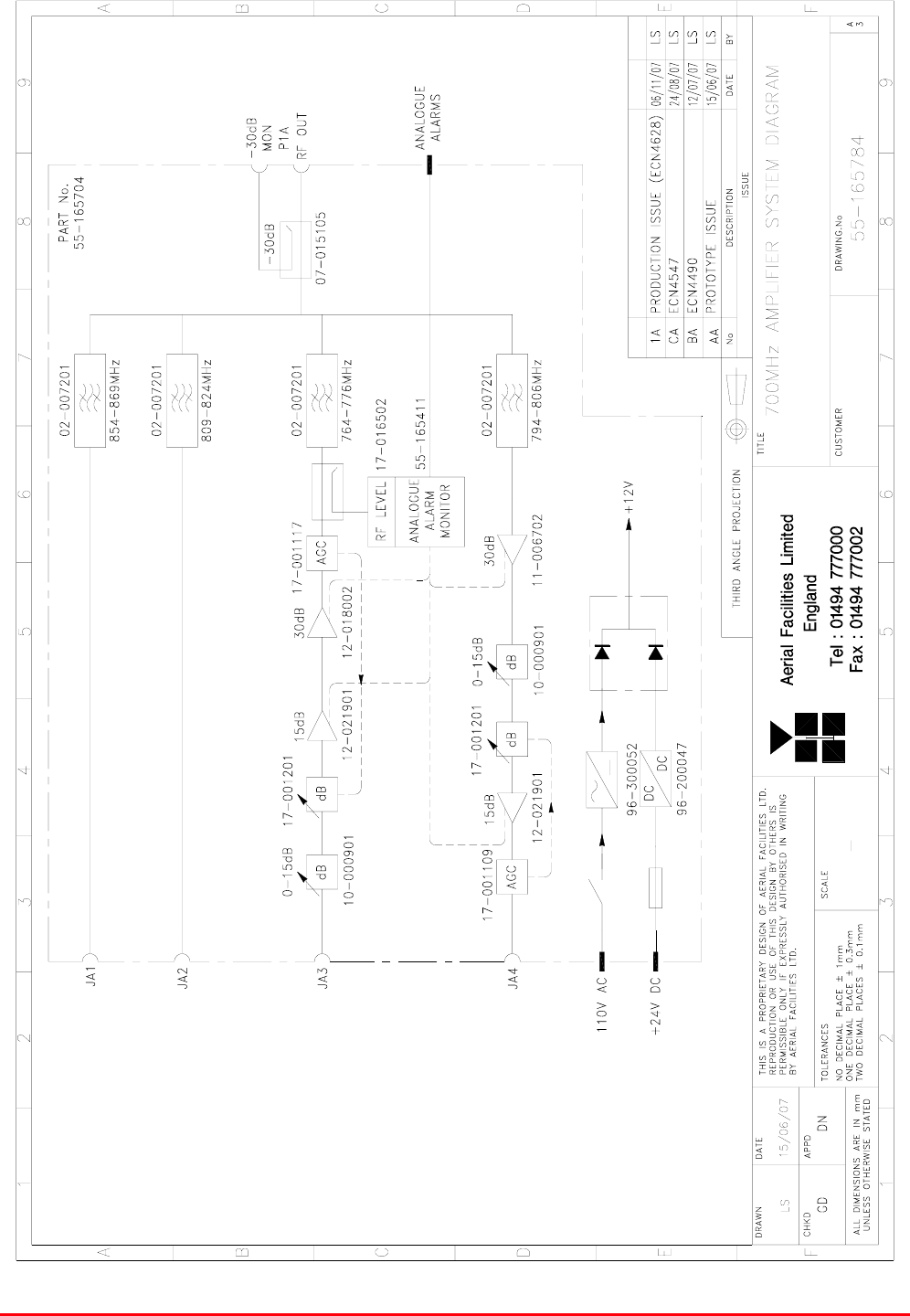
16.4.2.2. 700MHz Line Amplifier (55-165704) System Diagram
Drawing number 55-165784
STTRS DOCUMENTATION
Document Number 80-330501HBKM – Issue A - Draft Page 275 of 500
16.4.2.3. Bandpass Filter (02-007206)
The bandpass filters are multi-section designs with a bandwidth dependent upon the passband
frequencies, (both tuned to customer requirements). The response shape is basically Chebyshev with
a passband design ripple of 0.1dB. The filters are of slot coupled, folded combline design, and are
carefully aligned during manufacture in order to optimise the insertion loss, VSWR and
intermodulation characteristics of the unit. The tuned elements are silver-plated to reduce surface
ohmic losses and maintain a good VSWR figure and 50Ω load at the input and output ports.
Being passive devices, the bandpass filters should have an extremely long operational life and require
no maintenance. Should a filter be suspect, it is usually most time efficient to replace the module
rather than attempt repair or re-tuning.
No adjustments should be attempted without full network sweep analysis facilities to monitor both
insertion loss and VSWR simultaneously.
02-007206 Specification
PARAMETER SPECIFICATION
Response type Chebyshev
Frequency range 800 - 950MHz *
Bandwidth 25MHz *
Number of sections 8
Insertion loss 1.2 dB
VSWR better than 1.2:1
Connectors SMA female
Power handling 100W max
operation -20°C to +60°C Temperature
range storage -40°C to +70°C
Weight 3 kg (typical) *tuned to Customer's specification
16.4.2.4. Wideband Asymmetric Coupler (07-015105)
The purpose of Wideband Asymmetric Coupler (07-015105) is to tap off a known portion (in this case
30dB) of RF signal from transmission lines and to combine them, for example through splitter units for
different purposes (alarms/monitoring etc.), whilst maintaining an accurate 50Ω load to all
ports/interfaces throughout the specified frequency range. They are known formally as directional
couplers as they couple power from the RF mainline in one direction only.
07-015105 Specification
PARAMETER SPECIFICATION
Construction Inductive air gap
Frequency 800-2500MHz
Through loss 0.4dB (typical)
Coupling level -30dB ±0.5dB
Isolation N/A
Weight <1.0kg
Connectors SMA, female
operation -20°C to +60°C
Temperature
range storage -40°C to +70°C
STTRS DOCUMENTATION
Document Number 80-330501HBKM – Issue A - Draft Page 276 of 500
16.4.2.5. Switched Attenuator 0.25W, 0 - 15dB (10-000901)
In many practical applications for Cell Enhancers etc., the gain in each path is found to be excessive.
Therefore, provision is made within the unit for the setting of attenuation in each path, to reduce the
gain.
10-000901 provides attenuation from 0 - 15dB in 2 dB steps The attenuation is simply set using the
four miniature toggle switches on the top of each unit. Each switch is clearly marked with the
attenuation it provides, and the total attenuation in line is the sum of the values switched in. They are
designed to maintain an accurate 50Ω impedance over their operating frequency at both input and
output.
10-000901 Specification
PARAMETER SPECIFICATION
Attenuation Values 0-15dB
Attenuation Steps 1, 2, 4 and 8dB
Power Handling 0.25 Watt
Attenuation Accuracy ± 1.0 dB
Frequency Range DC to 1GHz
Impedance 50Ω
Connectors SMA
VSWR 1.3:1
Weigh 0.2kg
operation -20°C to +60°C Temperature
range storage -40°C to +70°C
16.4.2.6. Low Noise Amplifier (11-006702)
The Gallium-Arsenide low noise amplifiers used in 700MHz Line Amplifier (55-165704) are double
stage, solid-state low noise amplifiers. Class A circuitry is used throughout the units to ensure
excellent linearity and extremely low noise over a very wide dynamic range. The active devices are
very moderately rated to provide a long trouble-free working life. There are no adjustments on these
amplifiers, and in the unlikely event of a failure, then the complete amplifier should be replaced. This
amplifier features its own in-built alarm system which gives a volt-free relay contact type alarm that is
easily integrated into the main alarm system.
11-006702 Specification
PARAMETER SPECIFICATION
Frequency range: 800 – 1000MHz
Bandwidth: <200MHz
Gain: 29dB (typical)
1dB Compression point: 20dBm
OIP3: 33dBm
Input/Output return loss: >18dB
Noise figure: 1.3dB (typical)
Power consumption: 180mA @ 24V DC
Supply voltage: 10-24V DC
Connectors: SMA female
operational: -10°C to +60°C
Temperature range: storage: -20°C to +70°C
Size: 90 x 55 x 30.2mm
Weight: 290gms (approximately)
STTRS DOCUMENTATION
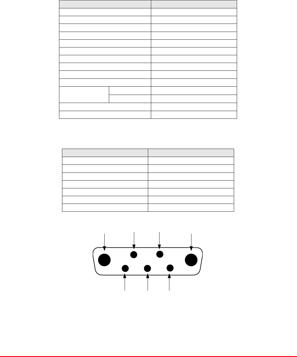
Document Number 80-330501HBKM – Issue A - Draft Page 277 of 500
7 8 96
1 2 3 4 5
9-Way Pin-Out Graphical Representation
Low Noise Amplifier (11-006702) ‘D’ Connector Pin-out details
Connector pin Signal
1 +Ve input (10-24V)
2 GND
3 Alarm RelayO/P bad
4 Alarm Relay common
5 Alarm Relay good
6 No connection
7 TTL voltage set
8 TTL alarm/0V (good)
9 O/C good/0V bad
16.4.2.7. Power Amplifier (12-018002)
This amplifier is a Class A 20W power amplifier from 800-960MHz in a 1 stage balanced
configuration. It demonstrates a very high linearity and a very good input/output return loss (RL). It
has built in a Current Fault Alarm Function.
Its housing is an aluminium case (Iridite NCP finish) with SMA connectors for the RF input/output and
a D-Type connector for the power supply and the Current Fault Alarm Function.
Technical Specification
PARAMETER SPECIFICATION
Frequency range: 800-960MHz
Small signal gain: 30dB
Gain flatness: ±1.2dB
I/O Return loss: >18dB
1dB compression point: 42.8dBm
OIP3: 56dBm
Supply voltage: 24V DC
Supply current: 5.0Amps (Typical)
operational: -10°C to +60°C Temperature
range storage: -20°C to +70°C
Weight: <2kg (no heatsink)
STTRS DOCUMENTATION
Document Number 80-330501HBKM – Issue A - Draft Page 278 of 500
Power Amplifier (12-018002) 7-Way Connector Pin-outs
Connector Pin Signal
A1 (large pin) +24V DC
A2 (large pin) GND
1 Alarm relay common
2 TTL alarm/0V good
3 Alarm relay contact (bad)
4 Alarm relay contact (good)
5 O/C good/0V bad (TTL)
16.4.2.8. Low Power Amplifier (12-021901)
The low power amplifier used is a triple stage solid-state low-noise amplifier. Class A circuitry is used
in the unit to ensure excellent linearity over a very wide dynamic range. The three active devices are
very moderately rated to provide a long trouble-free working life.
Its housing is an aluminium case (Iridite NCP finish) with SMA connectors for the RF input/output and
a D-Type connector for the power supply and the Current Fault Alarm Function.
There are no adjustments on this amplifier, and in the unlikely event of failure then the entire amplifier
should be replaced.
Low Power Amplifier (12-021901) Specification
PARAMETER SPECIFICATION
Frequency range 800-960MHz*
Bandwidth 20MHz *
Maximum RF output >1.0 Watt
Gain 15dB
1dB compression point +30.5dBm
3rd order intercept point +43dBm
Noise Figure <6dB
VSWR better than 1.5:1
Connectors SMA female
Supply 500mA @ 10-15V DC
operational -10°C to +60°C
Temperature
range storage -20°C to +70°C
Weight 0.5 kg
Size 167x52x25mm
* Tuned to Customer’s specification

STTRS DOCUMENTATION
Document Number 80-330501HBKM – Issue A - Draft Page 279 of 500
Low Power Amplifier (12-021901) 7-Way Connector Pin-outs
Connector Pin Signal
A1 (large pin) +24V DC
A2 (large pin) GND
1 Alarm relay common
2 TTL alarm/0V good
3 Alarm relay contact (bad)
4 Alarm relay contact (good)
5 O/C good/0V bad (TTL)
16.4.2.9. Automatic Gain Control
17-001109 AGC Detector Assembly (Logarithmic)
17-001117 AGC Detector Assembly
17-001201 AGC Attenuator Assembly
The sub components 17-001109, 17-001117 & 17-001201 are parts of the Automatic Gain Control
(AGC) system used in 700MHz Line Amplifier (55-165704); 17-001117 and 17-001201 are paired for
use in the uplink and 17-001109 and 17-001201 are paired for use in the downlink
700MHz Line Amplifier (55-165704) is fitted with two differing types of Automatic Gain Control (AGC)
system, one linear, and one logarithmic. The AGC with logarithmic detector (17-001117) is fitted in the
uplink path and the AGC with linear detector (17-001109) is fitted in the downlink path
The AFL Automatic Gain Control system consists of two units, a detector/amplifier and an attenuator.
The detector/amplifier unit is inserted in the RF path on the output of the power amplifier, and the
attenuator is situated in the RF path between the 1st and 2nd stages of amplification.
17-001117 and 17-001201 are paired for use in the uplink and 17-001109 and 17-001201 are paired
for use in the downlink
The attenuator comprises a 50Ω P.I.N diode, voltage-variable attenuator with a range of 3 to 30dB.
The attenuation is controlled by a DC voltage which is derived from the associated detector controller
board.
Normally the attenuator is at minimum attenuation. The detector/amplifier unit monitors the RF level
being delivered by the power amplifier, and when a certain threshold is reached it begins to increase
the value of the attenuator to limit the RF output to the (factory set) threshold. Therefore overloading
of the power amplifier is avoided.
The factory set threshold is 1dB below the Enhancer 1dB compression point. Some adjustment of this
AGC threshold level is possible, a 10dB range is mostly achieved. It is not recommended under any
circumstances to adjust the AGC threshold to a level greater than the 1dB compression point as
system degradation will occur.
STTRS DOCUMENTATION
Document Number 80-330501HBKM – Issue A - Draft Page 280 of 500
The detector comprises of a 50Ω transmission line with a resistive tap which samples a small portion
of the mainline power. The sampled signal is amplified and fed to a conventional half wave diode
rectifier, the output of which is a DC voltage proportional to the RF input signal.
This DC voltage is passed via an inverting DC amplifier with integrating characteristics, to the output,
which drives the attenuation control line of the corresponding AGC attenuator. This unit is fitted at
some earlier point in the RF circuit.
For small signals, below AGC onset, the output control line will be close to 12V and the AGC
attenuator will have minimum attenuation. As the signal level increases the control line voltage will
fall, increasing the attenuator value and keeping the system output level at a constant value.
AGC Specification (both types)
PARAMETER SPECIFICATION
Frequency range up to 1000MHz
Attenuation range 3 to 30dB
Attenuation steps continuously variable
VSWR better than 1.2:1
RF Connectors SMA female
attenuator 1W Power
handling detector/amp >30W (or as required)
operation -10°C to +60°C Temperature
range storage -20°C to +70°C
attenuator pcb 50 x 42 x 21mm
Size detector/amp pcb 54 x 42 x 21mm
attenuator 90grams
Weight detector/amp 100grams
16.4.2.10. 12V (Single) Relay Board (80-008901)
The General Purpose Relay Board allows the inversion of signals and the isolation of circuits. It is
equipped with a single dual pole change-over relay RL1, with completely isolated wiring, accessed
via a 15 way in-line connector.
The relay is provided with polarity protection diodes and diodes for suppressing the transients caused
by "flywheel effect" which can destroy switching transistors or induce spikes on neighbouring circuits.
It’s common use is to amalgamate all the alarm signals into one, volts-free relay contact pair for the
main alarm system.
80-008901 Specification
PARAMETER SPECIFICATION
Operating voltage 8 to 30V (floating earth)
Alarm threshold Vcc - 1.20 volt +15%
Alarm output relay contacts:
Max. switch current 1.0Amp
Max. switch volts 120Vdc/60VA
Max. switch power 24W/60VA
Min. switch load 10.0µA/10.0mV
Relay isolation 1.5kV
Mechanical life >2x10⁷ operations
Relay approval BT type 56
Connector details Screw terminals
operational -10°C to +60°C Temperature
range storage -20°C to +70°C
STTRS DOCUMENTATION
Document Number 80-330501HBKM – Issue A - Draft Page 281 of 500
16.4.2.11. Dual Diode Assembly (94-100004)
The purpose of these dual diode assemblies is to allow two DC voltage sources to be combined, so
that the main DC rail within the equipment can be sourced from either a mains driven PSU, or
externally through an XLR connector or from dual mains driven PSUs . They are very heavy-duty
diodes and they prevent any reverse current from flowing back to their source or the alternative
supply rail. Combining diodes such as these will also be used if the equipment is to be powered from
external back-up batteries.
16.4.2.12. DC/DC Converter 96-200047
96-200047 is an O.E.M. high power device with a wide input range and 12.5 amp @ 12V (150Watts)
output capability used to derive a 12V fixed voltage power supply rail from a higher voltage supply, in
this case 12V. In the event of failure this unit should not be repaired, only replaced.
96-200047 Specification
PARAMETER SPECIFICATION
DC Input Voltage range 19 to 36V
DC Output voltage 12V ± 1%
Max. current load 12.5Amps
Operation -10°C to +60°C Temperature
range Storage -20°C to +85°C
Working Humidity 20 to 90% RHNC
16.3.2.13. 12V Switch-Mode PSU (96-300052)
No routine maintenance of the PSU is required. If a fault is suspected, then the output voltage from
the power supply may be measured on its output terminals. This is typically set to 12.2V. The
adjustment potentiometer will be found close to the DC output terminals.
All the PSUs used in AFL Cell Enhancers are capable of operation from either 110 or 220V nominal
AC supplies. The line voltage is sensed automatically, so no adjustment or link setting is needed by
the operator.
96-300052 Specification
AC Input Supply 110 or 220V nominal
Voltage 85 - 265V AC
(absolute limits)
Frequency 47 to 63Hz
DC Output Supply 12V DC (nominal)
Voltage 10.5-13.8V (absolute limits)
Current 12.5A

STTRS DOCUMENTATION
Document Number 80-330501HBKM – Issue A - Draft Page 282 of 500
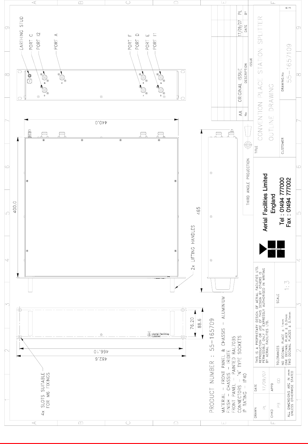
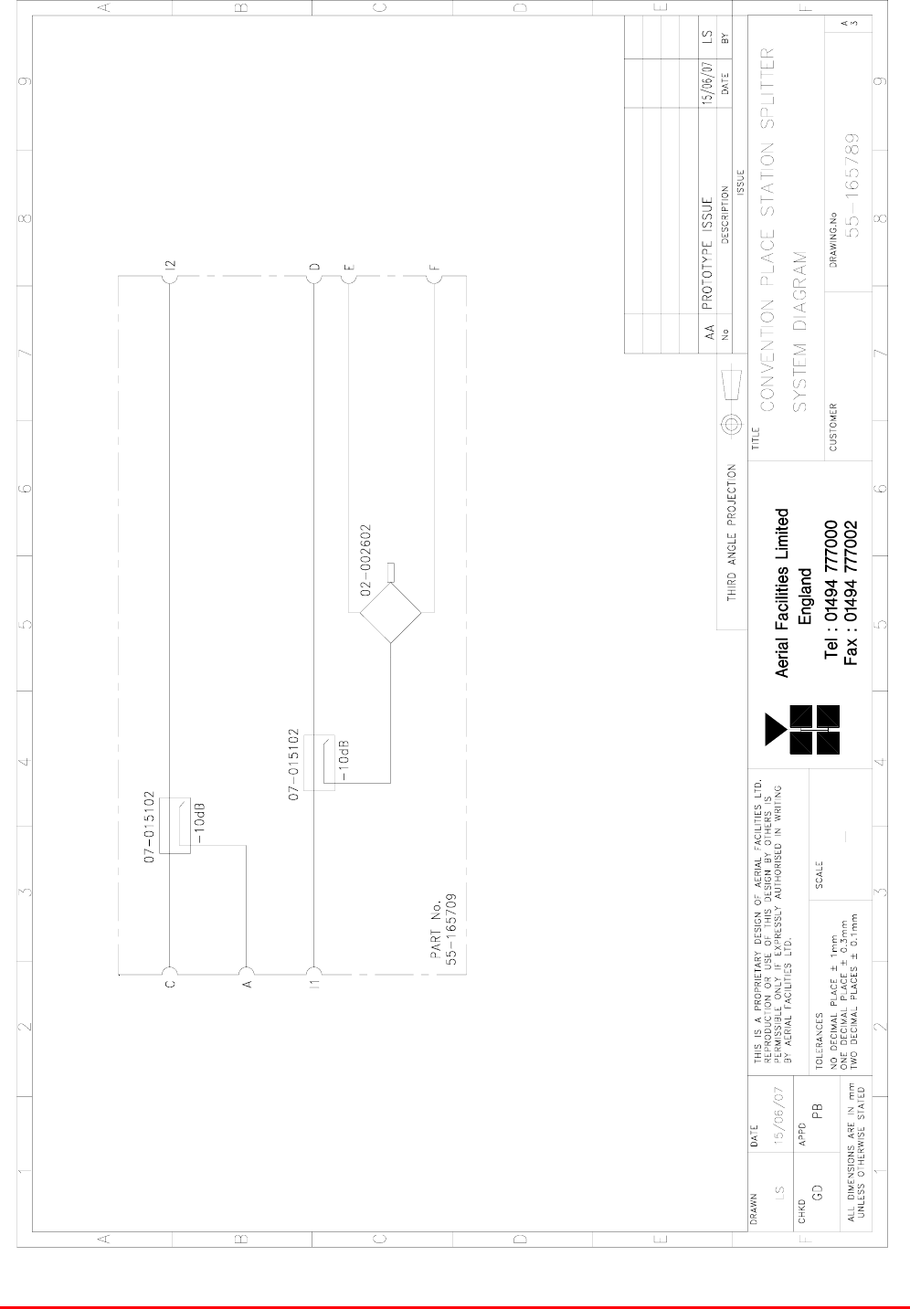
16.4.3. Convention Place Station Splitter (55-165709)
2U rack mount tray
Convention Place Station Splitter (55-165709) major components
Section Component
Part Component Part Description Qty. Per
Assembly
16.4.3.3. 05-002602 900MHz Splitter/Combiner 1
16.4.3.4. 07-015102 Wideband Asymmetric Coupler 2
STTRS DOCUMENTATION
Document Number 80-330501HBKM – Issue A - Draft Page 283 of 500
16.4.3.1. Convention Place Station Splitter (55-165709) outline drawing
Drawing number 55-1657109
STTRS DOCUMENTATION
Document Number 80-330501HBKM – Issue A - Draft Page 284 of 500
16.4.3.2. Convention Place Station Splitter (55-165709) system diagram
Drawing number 55-165789
STTRS DOCUMENTATION
Document Number 80-330501HBKM – Issue A - Draft Page 285 of 500
16.4.3.3. 900MHz Splitter/Combiner (05-002602)
The Splitter/Combiner used is a device for accurately matching two or more RF signals to single or
multiple ports, whilst maintaining an accurate 50Ω load to all inputs/outputs and ensuring that the
VSWR and insertion losses are kept to a minimum. Any unused ports should be terminated with an
appropriate 50Ω load.
Being passive devices, the splitters should have an extremely long operational life and require no
maintenance. Should a unit be suspect, it is usually most time efficient to replace the whole module
rather than attempt repair or re-tuning.
05-002602 Specification
PARAMETER SPECIFICATION
Narrowband: 815 – 960MHz Frequency
range: Broadband: 800 – 1200MHz
Narrowband: 145MHz
Bandwidth: Broadband: 400MHz
Input ports: 1
Output ports: 2
Narrowband: 3.3dB
Insertion loss: Broadband: 3.5dB
Return loss input & output: 1.3:1
Impedance: 50Ω
Narrowband: >20dB
Isolation: Broadband: >18dB
MTFB: >180,000 hours
Splitting: 20Watts
Power rating: Combining: 0.5Watt
Connectors: SMA female
Weight: 200g (approximately)
Size: 54 x 44 x 21mm
16.4.3.4. Wideband Asymmetric Coupler (07-015102)
The purpose of Wideband Asymmetric Coupler (07-015102) is to tap off a known portion (in this case
10dB) of RF signal from transmission lines and to combine them, for example through splitter units for
different purposes (alarms/monitoring etc.), whilst maintaining an accurate 50Ω load to all
ports/interfaces throughout the specified frequency range. They are known formally as directional
couplers as they couple power from the RF mainline in one direction only.
07-015102 Specification
PARAMETER SPECIFICATION
Frequency Range 800 - 2500 MHz
Coupling Value 10 dB ± 1.0 dB
Main Line Insertion Loss <1.6 dB
VSWR 1.4:1
Directivity >18 dB
Power Rating 200 Watts
RF Connectors ‘N’ female
operation -20°C to +60°C
Temperature
range storage -40°C to +70°C

STTRS DOCUMENTATION
Document Number 80-330501HBKM – Issue A - Draft Page 286 of 500
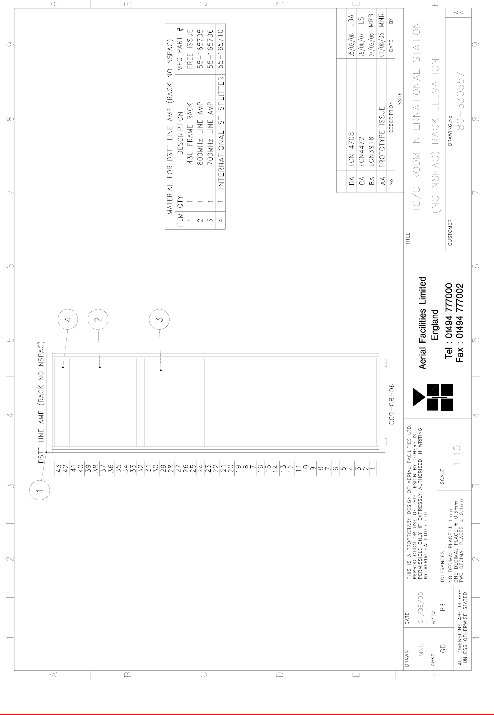
17. INTERNATIONAL (NO NPSPAC) LINE AMPLIFIER (80-330557)
Rack C09-CR-06
International (no NPSPAC) Line Amp. (80-330557) list of major components
Section Component
Part Component Part Description Qty. Per
Assembly
17.4.1. 55-165705 800MHz Line Amplifier (NO NSP) 1
17.4.2. 55-165706 700MHz Line Amplifier (NO NSP) 1
17.4.3. 55-165710 International Station Splitter 1
STTRS DOCUMENTATION
Document Number 80-330501HBKM – Issue A - Draft Page 287 of 500
17.1. International (no NPSPAC) Line Amp. (80-330557) Rack elevation
Drawing number 80-330557
STTRS DOCUMENTATION
Document Number 80-330501HBKM – Issue A - Draft Page 288 of 500
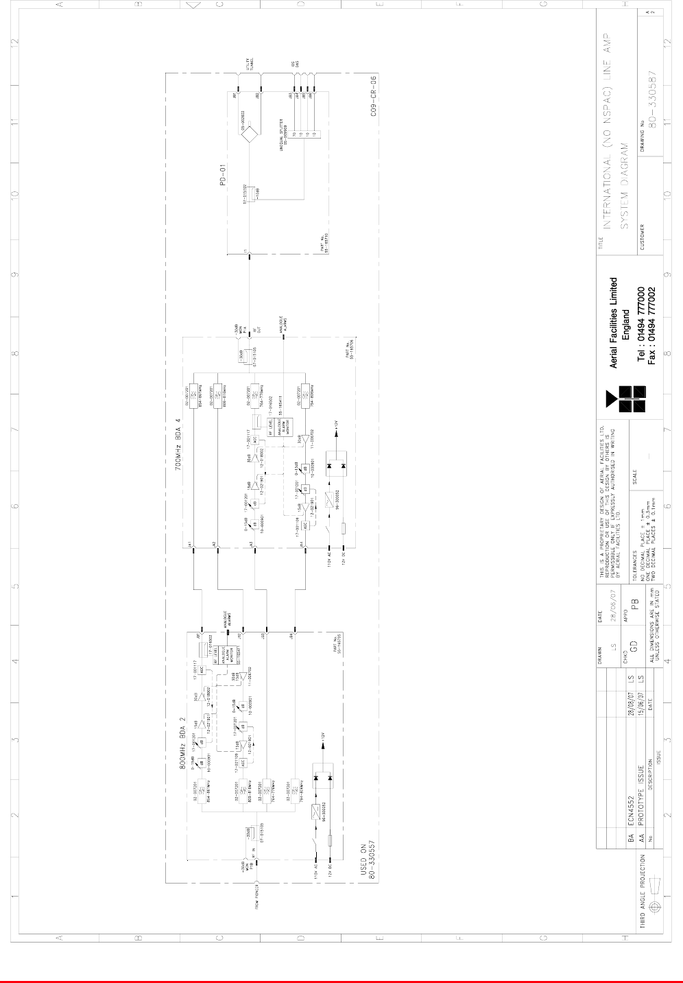
17.2. International (no NPSPAC) Line Amp. (80-330557) System diagram
Drawing number 80-330587
STTRS DOCUMENTATION
Document Number 80-330501HBKM – Issue A - Draft Page 289 of 500
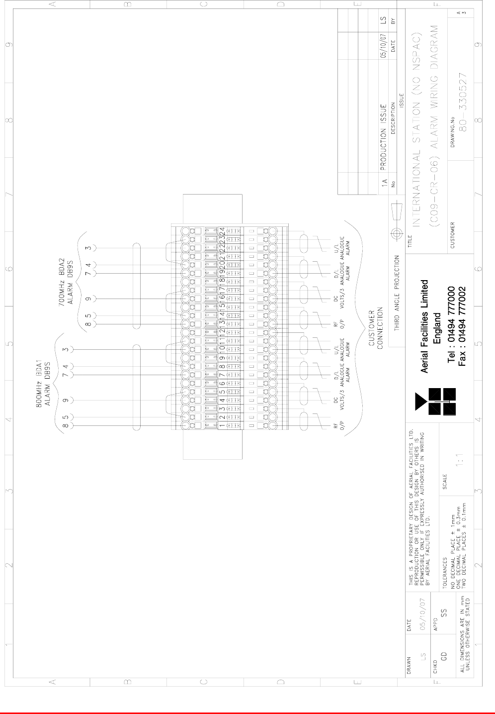
17.3. International (no NPSPAC) Line Amp. (80-330557) Alarm wiring diagram
Drawing number 80-330527

STTRS DOCUMENTATION
Document Number 80-330501HBKM – Issue A - Draft Page 290 of 500
17.4. International (no NPSPAC) Line Amp. (80-330557) major components
17.4.1. 800MHz Line Amplifier (no NPSPAC) (55-165705)
800MHz Line Amplifier (no NPSPAC) (55-165705) List of Major Components
section Component
Part Component Part Description Qty. Per
Assembly
17.4.1.3. 02-007201 Bandpass Filter 2
17.4.1.4. 02-007206 Bandpass Filter 2
17.4.1.5. 07-015105 Wideband Asymmetric Coupler 1
17.4.1.6. 10-000901 Switched Attenuator 0.25W, 0 - 15dB 2
17.4.1.7. 11-006702 Low Noise Amplifier 1
17.4.1.8. 12-018002 Power Amplifier 1
17.4.1.9. 12-021901 Low Power Amplifier 2
17-001109* AGC Detector Assembly (Logarithmic) 1
17-001117* AGC Detector Assembly 1
17.4.1.10.
17-001201* AGC Attenuator Assembly 2
17.4.1.11. 80-008901 12V (Single) Relay Board 1
17.4.1.12. 94-100004 Dual Diode Assembly 1
17.4.1.13. 96-200047 DC/DC Converter
17.4.1.14. 96-300052 12V Switch-Mode PSU (96-300052) 1
*The sub components 17-001109, 17-001117 & 17-001201 are parts of the Automatic Gain Control
(AGC) system used in 800MHz Line Amplifier (no NPSPAC) (55-165705); 17-001117 and 17-001201
are paired for use in the uplink and 17-001109 and 17-001201 are paired for use in the downlink
STTRS DOCUMENTATION
Document Number 80-330501HBKM – Issue A - Draft Page 291 of 500
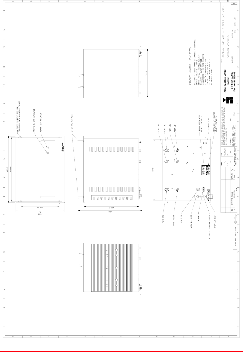
17.4.1.1. 800MHz Line Amplifier (no NPSPAC) (55-165705) Outline Drawing
Drawing number 55-1657105
STTRS DOCUMENTATION
Document Number 80-330501HBKM – Issue A - Draft Page 292 of 500
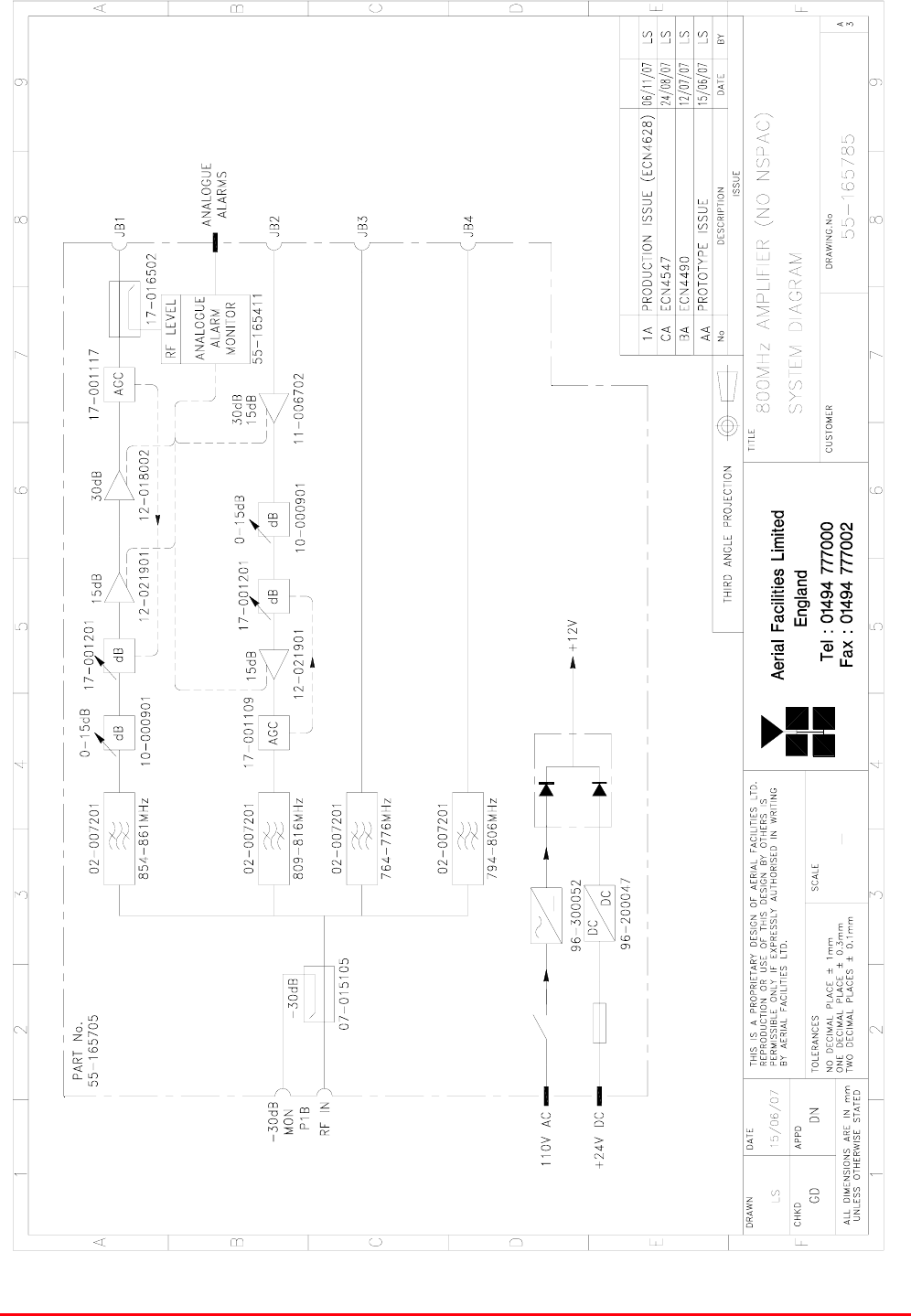
14.4.1.2. 800MHz Line Amplifier (no NPSPAC) (55-165705) System Diagram
Drawing number 55-165785

STTRS DOCUMENTATION
Document Number 80-330501HBKM – Issue A - Draft Page 293 of 500
17.4.1.3. Bandpass Filter (02-012701)
The bandpass filters are multi-section designs with a bandwidth dependent upon the passband
frequencies, (both tuned to customer requirements). The response shape is basically Chebyshev with
a passband design ripple of 0.1dB. The filters are of combline design and are carefully aligned during
manufacture in order to optimise the insertion loss, VSWR and intermodulation characteristics of the
unit. The tuned elements are silver-plated to reduce surface ohmic losses and maintain a good VSWR
figure and 50Ω load at the input and output ports. Being passive devices, the bandpass filters should
have an extremely long operational life and require no maintenance. Should a filter be suspect, it is
usually most time efficient to replace the module rather than attempt repair or re-tuning.
No adjustments should be attempted without full network sweep analysis facilities to monitor both
insertion loss and VSWR simultaneously.
02-012701 Specification PARAMETER SPECIFICATION
Frequency range 1805 – 1880 MHz *
Insertion loss <0.6 dB
>60 dB over 1710 – 1785 MHz
Rejection >40 dB over 1905 – 2170 MHz
Return loss > 20 dB
Power handling 200W (CW)
operation -20°C to +60°C Temperature
range storage -40°C to +70°C
Size 227 x 95 x 60mm (case only)
* tuned to customer’s specification
17.4.1.4. Bandpass Filter (02-007206)
The bandpass filters are multi-section designs with a bandwidth dependent upon the passband
frequencies, (both tuned to customer requirements). The response shape is basically Chebyshev with
a passband design ripple of 0.1dB. The filters are of slot coupled, folded combline design, and are
carefully aligned during manufacture in order to optimise the insertion loss, VSWR and
intermodulation characteristics of the unit. The tuned elements are silver-plated to reduce surface
ohmic losses and maintain a good VSWR figure and 50Ω load at the input and output ports. Being
passive devices, the bandpass filters should have an extremely long operational life and require no
maintenance. Should a filter be suspect, it is usually most time efficient to replace the module rather
than attempt repair or re-tuning.
No adjustments should be attempted without full network sweep analysis facilities to monitor both
insertion loss and VSWR simultaneously.
02-007206 Specification
PARAMETER SPECIFICATION
Response type Chebyshev
Frequency range 800 - 950MHz *
Bandwidth 25MHz *
Number of sections 8
Insertion loss 1.2 dB
VSWR better than 1.2:1
Connectors SMA female
Power handling 100W max
operation -20°C to +60°C Temperature
range storage -40°C to +70°C
Weight 3 kg (typical) *tuned to Customer's specification

STTRS DOCUMENTATION
Document Number 80-330501HBKM – Issue A - Draft Page 294 of 500
17.4.1.5. Wideband Asymmetric Coupler (07-015105)
The purpose of Wideband Asymmetric Coupler (07-015105) is to tap off a known portion (in this case
30dB) of RF signal from transmission lines and to combine them, for example through splitter units for
different purposes (alarms/monitoring etc.), whilst maintaining an accurate 50Ω load to all
ports/interfaces throughout the specified frequency range. They are known formally as directional
couplers as they couple power from the RF mainline in one direction only.
07-015105 Specification
PARAMETER SPECIFICATION
Construction Inductive air gap
Frequency 800-2500MHz
Through loss 0.4dB (typical)
Coupling level -30dB ±0.5dB
Isolation N/A
Weight <1.0kg
Connectors SMA, female
operation -20°C to +60°C
Temperature
range storage -40°C to +70°C
17.4.1.6. Switched Attenuator 0.25W, 0 - 15dB (10-000901)
In many practical applications for Cell Enhancers etc., the gain in each path is found to be excessive.
Therefore, provision is made within the unit for the setting of attenuation in each path, to reduce the
gain.
10-000901 provides attenuation from 0 - 15dB in 2 dB steps The attenuation is simply set using the
four miniature toggle switches on the top of each unit. Each switch is clearly marked with the
attenuation it provides, and the total attenuation in line is the sum of the values switched in. They are
designed to maintain an accurate 50Ω impedance over their operating frequency at both input and
output.
10-000901 Specification
PARAMETER SPECIFICATION
Attenuation Values 0-15dB
Attenuation Steps 1, 2, 4 and 8dB
Power Handling 0.25 Watt
Attenuation Accuracy ± 1.0 dB
Frequency Range DC to 1GHz
Impedance 50Ω
Connectors SMA
VSWR 1.3:1
Weigh 0.2kg
operation -20°C to +60°C Temperature
range storage -40°C to +70°C
STTRS DOCUMENTATION
Document Number 80-330501HBKM – Issue A - Draft Page 295 of 500
7 8 96
1 2 3 4 5
9-Way Pin-Out Graphical Representation
17.4.1.7. Low Noise Amplifier (11-006702)
The Gallium-Arsenide low noise amplifiers used in 800MHz Line Amplifier (55-165703) are double
stage, solid-state low noise amplifiers. Class A circuitry is used throughout the units to ensure
excellent linearity and extremely low noise over a very wide dynamic range. The active devices are
very moderately rated to provide a long trouble-free working life. There are no adjustments on these
amplifiers, and in the unlikely event of a failure, then the complete amplifier should be replaced. This
amplifier features its own in-built alarm system which gives a volt-free relay contact type alarm that is
easily integrated into the main alarm system.
11-006702 Specification
PARAMETER SPECIFICATION
Frequency range 800 – 1000MHz
Bandwidth <200MHz
Gain 29dB (typical)
1dB Compression point 20dBm
OIP3 33dBm
Input/Output return loss >18dB
Noise figure 1.3dB (typical)
Power consumption 180mA @ 24V DC
Supply voltage 10-24V DC
Connectors SMA female
operational -10°C to +60°C
Temperature range: storage -20°C to +70°C
Size 90 x 55 x 30.2mm
Weight 290gms (approximately)
Low Noise Amplifier (11-006702) ‘D’ Connector Pin-out details
Connector pin Signal
1 +Ve input (10-24V)
2 GND
3 Alarm RelayO/P bad
4 Alarm Relay common
5 Alarm Relay good
6 No connection
7 TTL voltage set
8 TTL alarm/0V (good)
9 O/C good/0V bad

STTRS DOCUMENTATION
Document Number 80-330501HBKM – Issue A - Draft Page 296 of 500
17.4.1.8. Power Amplifier (12-018002)
This amplifier is a Class A 20W power amplifier from 800-960MHz in a 1 stage balanced
configuration. It demonstrates a very high linearity and a very good input/output return loss (RL). It
has built in a Current Fault Alarm Function.
Its housing is an aluminium case (Iridite NCP finish) with SMA connectors for the RF input/output and
a D-Type connector for the power supply and the Current Fault Alarm Function.
12-018002 Specification
PARAMETER SPECIFICATION
Frequency range: 800-960MHz
Small signal gain: 30dB
Gain flatness: ±1.2dB
I/O Return loss: >18dB
1dB compression point: 42.8dBm
OIP3: 56dBm
Supply voltage: 24V DC
Supply current: 5.0Amps (Typical)
operational: -10°C to +60°C Temperature
range storage: -20°C to +70°C
Weight: <2kg (no heatsink)
Power Amplifier (12-018002) 7-Way Connector Pin-outs
Connector Pin Signal
A1 (large pin) +24V DC
A2 (large pin) GND
1 Alarm relay common
2 TTL alarm/0V good
3 Alarm relay contact (bad)
4 Alarm relay contact (good)
5 O/C good/0V bad (TTL)

STTRS DOCUMENTATION
Document Number 80-330501HBKM – Issue A - Draft Page 297 of 500
17.4.1.9. Low Power Amplifier (12-021901)
The low power amplifier used is a triple stage solid-state low-noise amplifier. Class A circuitry is used
in the unit to ensure excellent linearity over a very wide dynamic range. The three active devices are
very moderately rated to provide a long trouble-free working life.
Its housing is an aluminium case (Iridite NCP finish) with SMA connectors for the RF input/output and
a D-Type connector for the power supply and the Current Fault Alarm Function.
There are no adjustments on this amplifier, and in the unlikely event of failure then the entire amplifier
should be replaced.
Low Power Amplifier (12-021901) Specification
PARAMETER SPECIFICATION
Frequency range 800-960MHz*
Bandwidth 20MHz *
Maximum RF output >1.0 Watt
Gain 15dB
1dB compression point +30.5dBm
3rd order intercept point +43dBm
Noise Figure <6dB
VSWR better than 1.5:1
Connectors SMA female
Supply 500mA @ 10-15V DC
operational -10°C to +60°C
Temperature
range storage -20°C to +70°C
Weight 0.5 kg
Size 167x52x25mm
* Tuned to Customer’s specification
Low Power Amplifier (12-021901) 7-Way Connector Pin-outs
Connector Pin Signal
A1 (large pin) +24V DC
A2 (large pin) GND
1 Alarm relay common
2 TTL alarm/0V good
3 Alarm relay contact (bad)
4 Alarm relay contact (good)
5 O/C good/0V bad (TTL)

STTRS DOCUMENTATION
Document Number 80-330501HBKM – Issue A - Draft Page 298 of 500
7.4.1.10. Automatic Gain Control
17-001109 AGC Detector Assembly (Logarithmic)
17-001117 AGC Detector Assembly
17-001201 AGC Attenuator Assembly
The sub components 17-001109, 17-001117 & 17-001201 are parts of the Automatic Gain Control
(AGC) system used in 800MHz Line Amplifier (no NPSPAC) (55-165705); 17-001117 and 17-001201
are paired for use in the uplink and 17-001109 and 17-001201 are paired for use in the downlink
800MHz Line Amplifier (no NPSPAC) (55-165705) is fitted with two differing types of Automatic Gain
Control (AGC) system, one linear, and one logarithmic. The AGC with logarithmic detector (17-
001117) is fitted in the uplink path and the AGC with linear detector (17-001109) is fitted in the
downlink path
The AFL Automatic Gain Control system consists of two units, a detector/amplifier and an attenuator.
The detector/amplifier unit is inserted in the RF path on the output of the power amplifier, and the
attenuator is situated in the RF path between the 1st and 2nd stages of amplification.
17-001117 and 17-001201 are paired for use in the uplink and 17-001109 and 17-001201 are paired
for use in the downlink
The attenuator comprises a 50Ω P.I.N diode, voltage-variable attenuator with a range of 3 to 30dB.
The attenuation is controlled by a DC voltage which is derived from the associated detector controller
board.
Normally the attenuator is at minimum attenuation. The detector/amplifier unit monitors the RF level
being delivered by the power amplifier, and when a certain threshold is reached it begins to increase
the value of the attenuator to limit the RF output to the (factory set) threshold. Therefore overloading
of the power amplifier is avoided.
The factory set threshold is 1dB below the Enhancer 1dB compression point. Some adjustment of this
AGC threshold level is possible, a 10dB range is mostly achieved. It is not recommended under any
circumstances to adjust the AGC threshold to a level greater than the 1dB compression point as
system degradation will occur.
The detector comprises of a 50Ω transmission line with a resistive tap which samples a small portion
of the mainline power. The sampled signal is amplified and fed to a conventional half wave diode
rectifier, the output of which is a DC voltage proportional to the RF input signal.
This DC voltage is passed via an inverting DC amplifier with integrating characteristics, to the output,
which drives the attenuation control line of the corresponding AGC attenuator. This unit is fitted at
some earlier point in the RF circuit.
For small signals, below AGC onset, the output control line will be close to 12V and the AGC
attenuator will have minimum attenuation. As the signal level increases the control line voltage will
fall, increasing the attenuator value and keeping the system output level at a constant value.
STTRS DOCUMENTATION
Document Number 80-330501HBKM – Issue A - Draft Page 299 of 500
AGC Specification (both types)
PARAMETER SPECIFICATION
Frequency range up to 1000MHz
Attenuation range 3 to 30dB
Attenuation steps continuously variable
VSWR better than 1.2:1
RF Connectors SMA female
attenuator 1W Power
handling detector/amp >30W (or as required)
operation -10°C to +60°C Temperature
range storage -20°C to +70°C
attenuator pcb 50 x 42 x 21mm
Size detector/amp pcb 54 x 42 x 21mm
attenuator 90grams
Weight detector/amp 100grams
17.4.1.11. 12V (Single) Relay Board (80-008901)
The General Purpose Relay Board allows the inversion of signals and the isolation of circuits. It is
equipped with a single dual pole change-over relay RL1, with completely isolated wiring, accessed
via a 15 way in-line connector.
The relay is provided with polarity protection diodes and diodes for suppressing the transients caused
by "flywheel effect" which can destroy switching transistors or induce spikes on neighbouring circuits.
It’s common use is to amalgamate all the alarm signals into one, volts-free relay contact pair for the
main alarm system.
80-008901 Specification
PARAMETER SPECIFICATION
Operating voltage 8 to 30V (floating earth)
Alarm threshold Vcc - 1.20 volt +15%
Alarm output relay contacts:
Max. switch current 1.0Amp
Max. switch volts 120Vdc/60VA
Max. switch power 24W/60VA
Min. switch load 10.0µA/10.0mV
Relay isolation 1.5kV
Mechanical life >2x10⁷ operations
Relay approval BT type 56
Connector details Screw terminals
operational -10°C to +60°C Temperature
range storage -20°C to +70°C
STTRS DOCUMENTATION
Document Number 80-330501HBKM – Issue A - Draft Page 300 of 500
17.4.1.12. Dual Diode Assembly (94-100004)
The purpose of these dual diode assemblies is to allow two DC voltage sources to be combined, so
that the main DC rail within the equipment can be sourced from either a mains driven PSU, or
externally through an XLR connector or from dual mains driven PSUs . They are very heavy-duty
diodes and they prevent any reverse current from flowing back to their source or the alternative
supply rail. Combining diodes such as these will also be used if the equipment is to be powered from
external back-up batteries.
17.4.1.13. DC/DC Converter 96-200047
96-200047 is an O.E.M. high power device with a wide input range and 12.5 amp @ 12V (150Watts)
output capability used to derive a 12V fixed voltage power supply rail from a higher voltage supply, in
this case 12V. In the event of failure this unit should not be repaired, only replaced.
96-200047 Specification
PARAMETER SPECIFICATION
DC Input Voltage range 19 to 36V
DC Output voltage 12V ± 1%
Max. current load 12.5Amps
Operation -10°C to +60°C Temperature
range Storage -20°C to +85°C
Working Humidity 20 to 90% RHNC
17.4.1.14. 12V Switch-Mode PSU (96-300052)
No routine maintenance of the PSU is required. If a fault is suspected, then the output
voltage from the power supply may be measured on its output terminals. This is typically set
to 12.2V. The adjustment potentiometer will be found close to the DC output terminals.
All the PSUs used in AFL Cell Enhancers are capable of operation from either 110 or 220V
nominal AC supplies. The line voltage is sensed automatically, so no adjustment or link
setting is needed by the operator.
96-300052 Specification
AC Input Supply 110 or 220V nominal
Voltage 85 - 265V AC
(absolute limits)
Frequency 47 to 63Hz
DC Output Supply 12V DC (nominal)
Voltage 10.5-13.8V (absolute limits)
Current 12.5A

STTRS DOCUMENTATION
Document Number 80-330501HBKM – Issue A - Draft Page 301 of 500
17.4.2. 700MHz Line Amplifier (no NPSPAC) (55-165706)
700MHz Line Amplifier (no NPSPAC) (55-165706) List of Major Components
Section Component
Part Component Part Description Qty. Per
Assembly
17.4.2.3. 02-007201 Bandpass Filter 2
17.4.2.4. 02-007206 Bandpass Filter 2
17.4.2.5. 07-015105 Wideband Asymmetric Coupler 1
17.4.2.6. 10-000901 Switched Attenuator 0.25W, 0 - 15dB 2
17.4.2.7. 11-006702 Low Noise Amplifier 1
17.4.2.8. 12-018002 Power Amplifier 1
17.4.1.9. 12-021901 Low Power Amplifier 2
17-001109 AGC Detector Assembly (Logarithmic) 1
17-001117 AGC Detector Assembly 1
17.4.2.10.
17-001201 AGC Attenuator Assembly 2
17.4.2.11. 80-008901 12V (Single) Relay Board 1
17.4.2.12. 94-100004 Dual Diode Assembly 1
17.4.2.13. 96-200047 DC/DC Converter
17.4.2.14. 96-300052 12V Switch-Mode PSU (96-300052) 1
*The sub components 17-001109, 17-001117 & 17-001201 are parts of the Automatic Gain Control
(AGC) system used in 700MHz Line Amplifier (no NPSPAC) (55-165705); 17-001117 and 17-001201
are paired for use in the uplink and 17-001109 and 17-001201 are paired for use in the downlink
STTRS DOCUMENTATION
Document Number 80-330501HBKM – Issue A - Draft Page 302 of 500
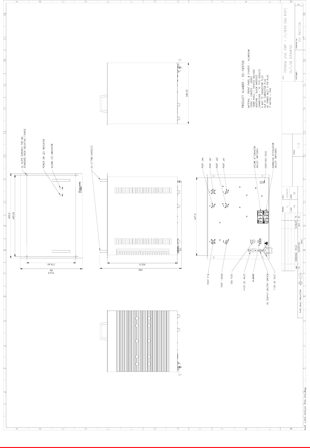
17.4.2.1. 700MHz Line Amplifier (no NPSPAC) (55-165706) Outline Drawing
Drawing number 55-1657106
STTRS DOCUMENTATION
Document Number 80-330501HBKM – Issue A - Draft Page 303 of 500
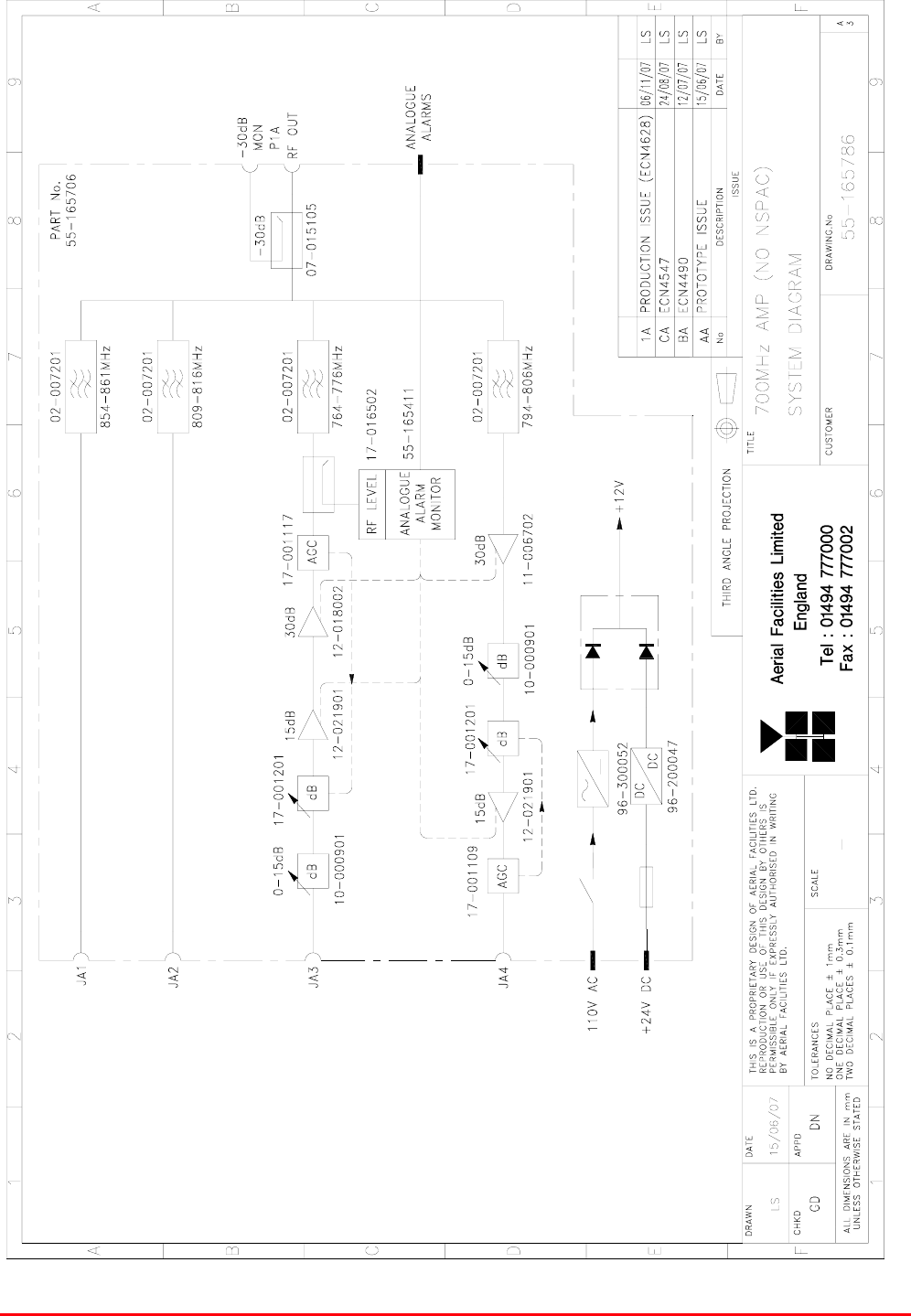
17.4.2.2. 700MHz Line Amplifier (no NPSPAC) (55-165706) System Diagram
Drawing number 55-165786
STTRS DOCUMENTATION
Document Number 80-330501HBKM – Issue A - Draft Page 304 of 500
17.4.2.3. Bandpass Filter (02-012701)
The bandpass filters are multi-section designs with a bandwidth dependent upon the passband
frequencies, (both tuned to customer requirements). The response shape is basically Chebyshev with
a passband design ripple of 0.1dB. The filters are of combline design and are carefully aligned during
manufacture in order to optimise the insertion loss, VSWR and intermodulation characteristics of the
unit. The tuned elements are silver-plated to reduce surface ohmic losses and maintain a good VSWR
figure and 50Ω load at the input and output ports. Being passive devices, the bandpass filters should
have an extremely long operational life and require no maintenance. Should a filter be suspect, it is
usually most time efficient to replace the module rather than attempt repair or re-tuning.
No adjustments should be attempted without full network sweep analysis facilities to monitor both
insertion loss and VSWR simultaneously.
02-012701 Specification PARAMETER SPECIFICATION
Frequency range 1805 – 1880 MHz *
Insertion loss <0.6 dB
>60 dB over 1710 – 1785 MHz
Rejection >40 dB over 1905 – 2170 MHz
Return loss > 20 dB
Power handling 200W (CW)
operation -20°C to +60°C Temperature
range storage -40°C to +70°C
Size 227 x 95 x 60mm (case only)
* tuned to customer’s specification
17.4.2.4. Bandpass Filter (02-007206)
The bandpass filters are multi-section designs with a bandwidth dependent upon the passband
frequencies, (both tuned to customer requirements). The response shape is basically Chebyshev with
a passband design ripple of 0.1dB. The filters are of slot coupled, folded combline design, and are
carefully aligned during manufacture in order to optimise the insertion loss, VSWR and
intermodulation characteristics of the unit. The tuned elements are silver-plated to reduce surface
ohmic losses and maintain a good VSWR figure and 50Ω load at the input and output ports. Being
passive devices, the bandpass filters should have an extremely long operational life and require no
maintenance. Should a filter be suspect, it is usually most time efficient to replace the module rather
than attempt repair or re-tuning.
No adjustments should be attempted without full network sweep analysis facilities to monitor both
insertion loss and VSWR simultaneously.
02-007206 Specification
PARAMETER SPECIFICATION
Response type Chebyshev
Frequency range 800 - 950MHz *
Bandwidth 25MHz *
Number of sections 8
Insertion loss 1.2 dB
VSWR better than 1.2:1
Connectors SMA female
Power handling 100W max
operation -20°C to +60°C Temperature
range storage -40°C to +70°C
Weight 3 kg (typical) *tuned to Customer's specification
STTRS DOCUMENTATION
Document Number 80-330501HBKM – Issue A - Draft Page 305 of 500
17.4.2.5. Wideband Asymmetric Coupler (07-015105)
The purpose of Wideband Asymmetric Coupler (07-015105) is to tap off a known portion (in this case
30dB) of RF signal from transmission lines and to combine them, for example through splitter units for
different purposes (alarms/monitoring etc.), whilst maintaining an accurate 50Ω load to all
ports/interfaces throughout the specified frequency range. They are known formally as directional
couplers as they couple power from the RF mainline in one direction only.
07-015105 Specification
PARAMETER SPECIFICATION
Construction Inductive air gap
Frequency 800-2500MHz
Through loss 0.4dB (typical)
Coupling level -30dB ±0.5dB
Isolation N/A
Weight <1.0kg
Connectors SMA, female
operation -20°C to +60°C
Temperature
range storage -40°C to +70°C
17.4.2.6. Switched Attenuator 0.25W, 0 - 15dB (10-000901)
In many practical applications for Cell Enhancers etc., the gain in each path is found to be excessive.
Therefore, provision is made within the unit for the setting of attenuation in each path, to reduce the
gain.
10-000901 provides attenuation from 0 - 15dB in 2 dB steps The attenuation is simply set using the
four miniature toggle switches on the top of each unit. Each switch is clearly marked with the
attenuation it provides, and the total attenuation in line is the sum of the values switched in. They are
designed to maintain an accurate 50Ω impedance over their operating frequency at both input and
output.
10-000901 Specification
PARAMETER SPECIFICATION
Attenuation Values 0-15dB
Attenuation Steps 1, 2, 4 and 8dB
Power Handling 0.25 Watt
Attenuation Accuracy ± 1.0 dB
Frequency Range DC to 1GHz
Impedance 50Ω
Connectors SMA
VSWR 1.3:1
Weigh 0.2kg
operation -20°C to +60°C Temperature
range storage -40°C to +70°C

STTRS DOCUMENTATION
Document Number 80-330501HBKM – Issue A - Draft Page 306 of 500
7 8 96
1 2 3 4 5
9-Way Pin-Out Graphical Representation
17.4.2.7. Low Noise Amplifier (11-006702)
The Gallium-Arsenide low noise amplifiers used in 800MHz Line Amplifier (55-165703) are double
stage, solid-state low noise amplifiers. Class A circuitry is used throughout the units to ensure
excellent linearity and extremely low noise over a very wide dynamic range. The active devices are
very moderately rated to provide a long trouble-free working life. There are no adjustments on these
amplifiers, and in the unlikely event of a failure, then the complete amplifier should be replaced. This
amplifier features its own in-built alarm system which gives a volt-free relay contact type alarm that is
easily integrated into the main alarm system.
11-006702 Specification
PARAMETER SPECIFICATION
Frequency range 800 – 1000MHz
Bandwidth <200MHz
Gain 29dB (typical)
1dB Compression point 20dBm
OIP3 33dBm
Input/Output return loss >18dB
Noise figure 1.3dB (typical)
Power consumption 180mA @ 24V DC
Supply voltage 10-24V DC
Connectors SMA female
operational -10°C to +60°C
Temperature range: storage -20°C to +70°C
Size 90 x 55 x 30.2mm
Weight 290gms (approximately)
Low Noise Amplifier (11-006702) ‘D’ Connector Pin-out details
Connector pin Signal
1 +Ve input (10-24V)
2 GND
3 Alarm RelayO/P bad
4 Alarm Relay common
5 Alarm Relay good
6 No connection
7 TTL voltage set
8 TTL alarm/0V (good)
9 O/C good/0V bad
STTRS DOCUMENTATION
Document Number 80-330501HBKM – Issue A - Draft Page 307 of 500
17.4.2.8. Power Amplifier (12-018002)
This amplifier is a Class A 20W power amplifier from 800-960MHz in a 1 stage balanced
configuration. It demonstrates a very high linearity and a very good input/output return loss (RL). It
has built in a Current Fault Alarm Function.
Its housing is an aluminium case (Iridite NCP finish) with SMA connectors for the RF input/output and
a D-Type connector for the power supply and the Current Fault Alarm Function.
12-018002 Specification
PARAMETER SPECIFICATION
Frequency range: 800-960MHz
Small signal gain: 30dB
Gain flatness: ±1.2dB
I/O Return loss: >18dB
1dB compression point: 42.8dBm
OIP3: 56dBm
Supply voltage: 24V DC
Supply current: 5.0Amps (Typical)
operational: -10°C to +60°C Temperature
range storage: -20°C to +70°C
Weight: <2kg (no heatsink)
Power Amplifier (12-018002) 7-Way Connector Pin-outs
Connector Pin Signal
A1 (large pin) +24V DC
A2 (large pin) GND
1 Alarm relay common
2 TTL alarm/0V good
3 Alarm relay contact (bad)
4 Alarm relay contact (good)
5 O/C good/0V bad (TTL)
STTRS DOCUMENTATION
Document Number 80-330501HBKM – Issue A - Draft Page 308 of 500
17.4.2.9. Low Power Amplifier (12-021901)
The low power amplifier used is a triple stage solid-state low-noise amplifier. Class A circuitry is used
in the unit to ensure excellent linearity over a very wide dynamic range. The three active devices are
very moderately rated to provide a long trouble-free working life.
Its housing is an aluminium case (Iridite NCP finish) with SMA connectors for the RF input/output and
a D-Type connector for the power supply and the Current Fault Alarm Function.
There are no adjustments on this amplifier, and in the unlikely event of failure then the entire amplifier
should be replaced.
Low Power Amplifier (12-021901) Specification
PARAMETER SPECIFICATION
Frequency range 800-960MHz*
Bandwidth 20MHz *
Maximum RF output >1.0 Watt
Gain 15dB
1dB compression point +30.5dBm
3rd order intercept point +43dBm
Noise Figure <6dB
VSWR better than 1.5:1
Connectors SMA female
Supply 500mA @ 10-15V DC
operational -10°C to +60°C
Temperature
range storage -20°C to +70°C
Weight 0.5 kg
Size 167x52x25mm
* Tuned to Customer’s specification
Low Power Amplifier (12-021901) 7-Way Connector Pin-outs
Connector Pin Signal
A1 (large pin) +24V DC
A2 (large pin) GND
1 Alarm relay common
2 TTL alarm/0V good
3 Alarm relay contact (bad)
4 Alarm relay contact (good)
5 O/C good/0V bad (TTL)

STTRS DOCUMENTATION
Document Number 80-330501HBKM – Issue A - Draft Page 309 of 500
7.4.2.10. Automatic Gain Control
17-001109 AGC Detector Assembly (Logarithmic)
17-001117 AGC Detector Assembly
17-001201 AGC Attenuator Assembly
The sub components 17-001109, 17-001117 & 17-001201 are parts of the Automatic Gain Control
(AGC) system used in 700MHz Line Amplifier (no NPSPAC) (55-165705); 17-001117 and 17-001201
are paired for use in the uplink and 17-001109 and 17-001201 are paired for use in the downlink
700MHz Line Amplifier (no NPSPAC) (55-165705) is fitted with two differing types of Automatic Gain
Control (AGC) system, one linear, and one logarithmic. The AGC with logarithmic detector (17-
001117) is fitted in the uplink path and the AGC with linear detector (17-001109) is fitted in the
downlink path
The AFL Automatic Gain Control system consists of two units, a detector/amplifier and an attenuator.
The detector/amplifier unit is inserted in the RF path on the output of the power amplifier, and the
attenuator is situated in the RF path between the 1st and 2nd stages of amplification.
17-001117 and 17-001201 are paired for use in the uplink and 17-001109 and 17-001201 are paired
for use in the downlink
The attenuator comprises a 50Ω P.I.N diode, voltage-variable attenuator with a range of 3 to 30dB.
The attenuation is controlled by a DC voltage which is derived from the associated detector controller
board.
Normally the attenuator is at minimum attenuation. The detector/amplifier unit monitors the RF level
being delivered by the power amplifier, and when a certain threshold is reached it begins to increase
the value of the attenuator to limit the RF output to the (factory set) threshold. Therefore overloading
of the power amplifier is avoided.
The factory set threshold is 1dB below the Enhancer 1dB compression point. Some adjustment of this
AGC threshold level is possible, a 10dB range is mostly achieved. It is not recommended under any
circumstances to adjust the AGC threshold to a level greater than the 1dB compression point as
system degradation will occur.
The detector comprises of a 50Ω transmission line with a resistive tap which samples a small portion
of the mainline power. The sampled signal is amplified and fed to a conventional half wave diode
rectifier, the output of which is a DC voltage proportional to the RF input signal.
This DC voltage is passed via an inverting DC amplifier with integrating characteristics, to the output,
which drives the attenuation control line of the corresponding AGC attenuator. This unit is fitted at
some earlier point in the RF circuit.
For small signals, below AGC onset, the output control line will be close to 12V and the AGC
attenuator will have minimum attenuation. As the signal level increases the control line voltage will
fall, increasing the attenuator value and keeping the system output level at a constant value.
STTRS DOCUMENTATION
Document Number 80-330501HBKM – Issue A - Draft Page 310 of 500
AGC Specification (both types)
PARAMETER SPECIFICATION
Frequency range up to 1000MHz
Attenuation range 3 to 30dB
Attenuation steps continuously variable
VSWR better than 1.2:1
RF Connectors SMA female
attenuator 1W Power
handling detector/amp >30W (or as required)
operation -10°C to +60°C Temperature
range storage -20°C to +70°C
attenuator pcb 50 x 42 x 21mm
Size detector/amp pcb 54 x 42 x 21mm
attenuator 90grams
Weight detector/amp 100grams
17.4.2.11. 12V (Single) Relay Board (80-008901)
The General Purpose Relay Board allows the inversion of signals and the isolation of circuits. It is
equipped with a single dual pole change-over relay RL1, with completely isolated wiring, accessed
via a 15 way in-line connector.
The relay is provided with polarity protection diodes and diodes for suppressing the transients caused
by "flywheel effect" which can destroy switching transistors or induce spikes on neighbouring circuits.
It’s common use is to amalgamate all the alarm signals into one, volts-free relay contact pair for the
main alarm system.
80-008901 Specification
PARAMETER SPECIFICATION
Operating voltage 8 to 30V (floating earth)
Alarm threshold Vcc - 1.20 volt +15%
Alarm output relay contacts
Max. switch current 1.0Amp
Max. switch volts 120Vdc/60VA
Max. switch power 24W/60VA
Min. switch load 10.0µA/10.0mV
Relay isolation 1.5kV
Mechanical life >2x10⁷ operations
Relay approval BT type 56
Connector details Screw terminals
operational -10°C to +60°C Temperature
range storage -20°C to +70°C
STTRS DOCUMENTATION
Document Number 80-330501HBKM – Issue A - Draft Page 311 of 500
17.4.2.12. Dual Diode Assembly (94-100004)
The purpose of these dual diode assemblies is to allow two DC voltage sources to be combined, so
that the main DC rail within the equipment can be sourced from either a mains driven PSU, or
externally through an XLR connector or from dual mains driven PSUs . They are very heavy-duty
diodes and they prevent any reverse current from flowing back to their source or the alternative
supply rail. Combining diodes such as these will also be used if the equipment is to be powered from
external back-up batteries.
17.4.2.13. DC/DC Converter 96-200047
96-200047 is an O.E.M. high power device with a wide input range and 12.5 amp @ 12V (150Watts)
output capability used to derive a 12V fixed voltage power supply rail from a higher voltage supply, in
this case 12V. In the event of failure this unit should not be repaired, only replaced.
96-200047 Specification
PARAMETER SPECIFICATION
DC Input Voltage range 19 to 36V
DC Output voltage 12V ± 1%
Max. current load 12.5Amps
Operation -10°C to +60°C Temperature
range Storage -20°C to +85°C
Working Humidity 20 to 90% RHNC
17.4.2.14. 12V Switch-Mode PSU (96-300052)
No routine maintenance of the PSU is required. If a fault is suspected, then the output voltage from
the power supply may be measured on its output terminals. This is typically set to 12.2V. The
adjustment potentiometer will be found close to the DC output terminals.
All the PSUs used in AFL Cell Enhancers are capable of operation from either 110 or 220V nominal
AC supplies. The line voltage is sensed automatically, so no adjustment or link setting is needed by
the operator.
96-300052 Specification
AC Input Supply 110 or 220V nominal
Voltage 85 - 265V AC
(absolute limits)
Frequency 47 to 63Hz
DC Output Supply 12V DC (nominal)
Voltage 10.5-13.8V (absolute limits)
Current 12.5A

STTRS DOCUMENTATION
Document Number 80-330501HBKM – Issue A - Draft Page 312 of 500
17.4.3. International Station Splitter (55-165710)
2U Rack mount tray
International Station Splitter (55-165710) List of major Components
Section Component
Part Component Part Description Qty. Per
Assembly
17.4.3.3. 05-002602 900MHZ SPLITTER/COMBINER, 20W 1
17.4.3.4. 05-009909 4 WAY POWER SPLITTER 70/10/10/10 1
17.4.3.5. 07-015102 Wideband Asymmetric Coupler 1
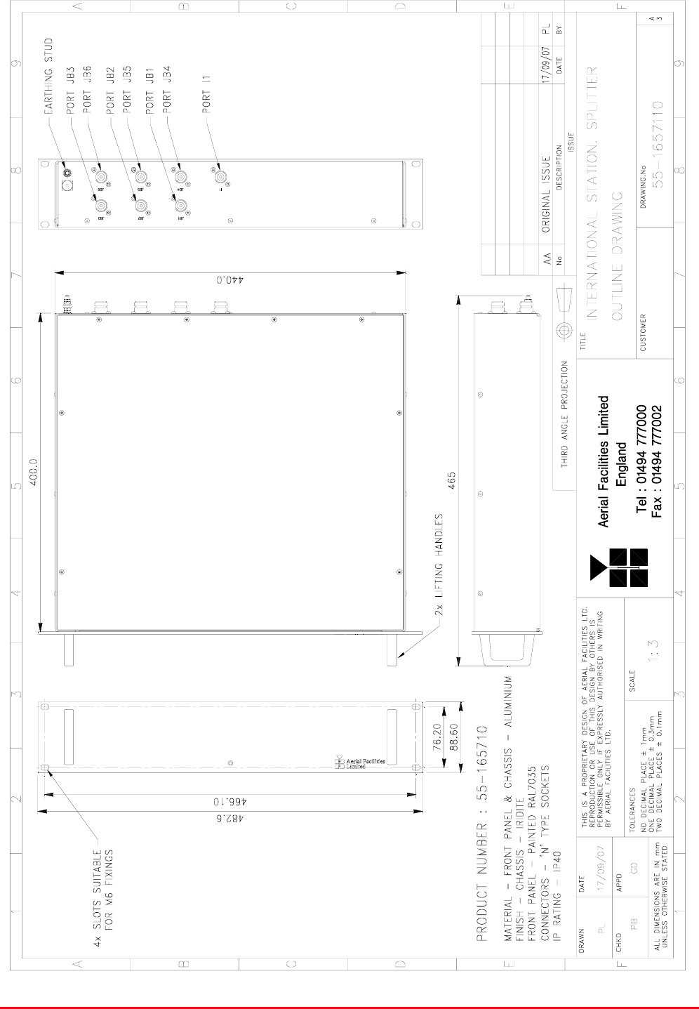
STTRS DOCUMENTATION
Document Number 80-330501HBKM – Issue A - Draft Page 313 of 500
17.4.3.1. International Station Splitter (55-165710) Outline drawing
Drawing number 55-1657110
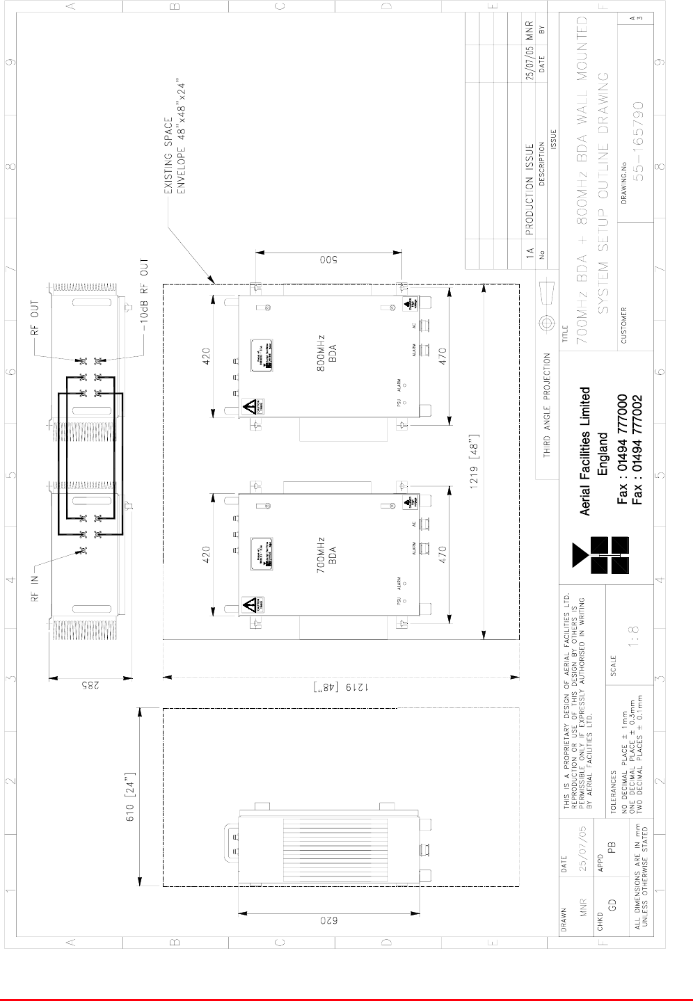
STTRS DOCUMENTATION
Document Number 80-330501HBKM – Issue A - Draft Page 314 of 500
17.4.3.2. International Station Splitter (55-165710) System Diagram
Drawing number 55-165790
STTRS DOCUMENTATION
Document Number 80-330501HBKM – Issue A - Draft Page 315 of 500
17.4.3.3. 900MHz Splitter/Combiner (05-002602)
The Splitter/Combiner used is a device for accurately matching two or more RF signals to single or
multiple ports, whilst maintaining an accurate 50Ω load to all inputs/outputs and ensuring that the
VSWR and insertion losses are kept to a minimum. Any unused ports should be terminated with an
appropriate 50Ω load.
Being passive devices, the splitters should have an extremely long operational life and require no
maintenance. Should a unit be suspect, it is usually most time efficient to replace the whole module
rather than attempt repair or re-tuning.
05-002602 Specification
PARAMETER SPECIFICATION
Narrowband 815 – 960MHz Frequency
range Broadband 800 – 1200MHz
Narrowband 145MHz
Bandwidth Broadband 400MHz
Input ports 1
Output ports 2
Narrowband 3.3dB
Insertion loss Broadband 3.5dB
Return loss input & output 1.3:1
Impedance 50Ω
Narrowband >20dB
Isolation Broadband >18dB
MTFB >180,000 hours
Splitting 20Watts
Power rating Combining 0.5Watt
Connectors SMA female
Weight 200g (approximately)
Size 54 x 44 x 21mm
17.4.3.4. 05-009909 – BSB to provide spec ***///***

STTRS DOCUMENTATION
Document Number 80-330501HBKM – Issue A - Draft Page 316 of 500
17.4.3.5. Wideband Asymmetric Coupler (07-015102)
The purpose of Wideband Asymmetric Coupler (07-015102) is to tap off a known portion (in this case
10dB) of RF signal from transmission lines and to combine them, for example through splitter units for
different purposes (alarms/monitoring etc.), whilst maintaining an accurate 50Ω load to all
ports/interfaces throughout the specified frequency range. They are known formally as directional
couplers as they couple power from the RF mainline in one direction only.
07-015102 Specification
PARAMETER SPECIFICATION
Frequency Range 800 - 2500 MHz
Coupling Value 10 dB ± 1.0 dB
Main Line Insertion Loss <1.6 dB
VSWR 1.4:1
Directivity >18 dB
Power Rating 200 Watts
RF Connectors ‘N’ female
operation -20°C to +60°C
Temperature
range storage -40°C to +70°C

STTRS DOCUMENTATION
Document Number 80-330501HBKM – Issue A - Draft Page 317 of 500
18. UNIVERSITY STATION CROSS PASSAGE A (80-330590-1)
Wallmount case
number C06-CR-01
University Station Cross Passage A (80-330590-1)
Section Component
Part Component Part Description Qty Per
Assembly
18.3.1. 07-015102 Wideband Asymmetric Coupler 1
18.3.2. 12-018002 Power Amplifier 2
18.3.3. 55-165701 800MHz Line Amplifier 1
18.3.4. 55-165702 700MHz Line Amplifier 1
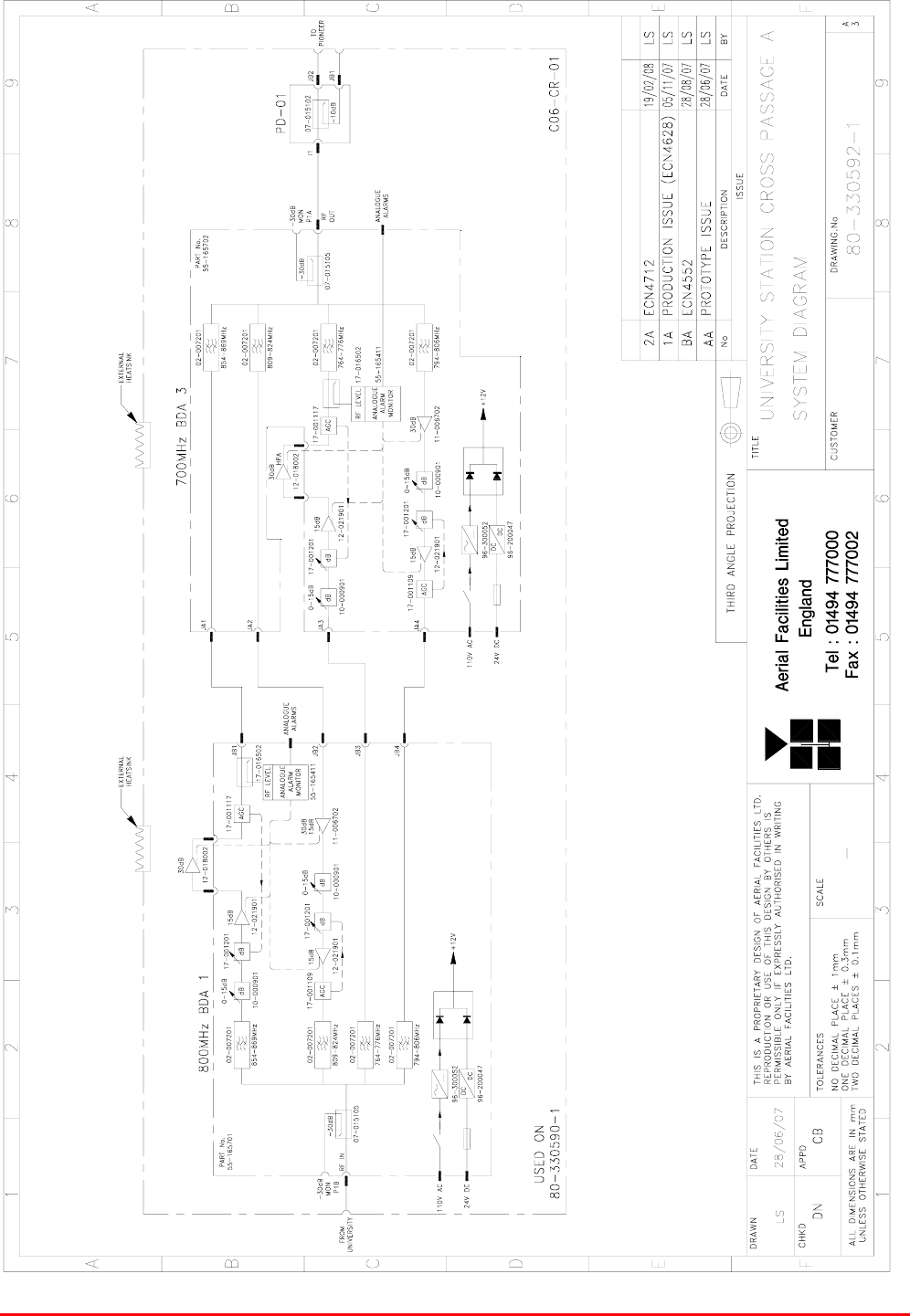
STTRS DOCUMENTATION
Document Number 80-330501HBKM – Issue A - Draft Page 318 of 500
18.1. University Station Cross Passage A (80-330590-1) System Diagram
Drawing number 80-330592-1

STTRS DOCUMENTATION
Document Number 80-330501HBKM – Issue A - Draft Page 319 of 500
18.2. University Station Cross Passage A (80-330590-1) Alarm Wiring Diagram
Drawing Number 80-330530-1

STTRS DOCUMENTATION
Document Number 80-330501HBKM – Issue A - Draft Page 320 of 500
18.3. University Station Cross Passage A (80-330590-1) Major Sub Components
18.3.1. Wideband Asymmetric Coupler (07-015102)
The purpose of Wideband Asymmetric Coupler (07-015102) is to tap off a known portion (in this case
10dB) of RF signal from transmission lines and to combine them, for example through splitter units for
different purposes (alarms/monitoring etc.), whilst maintaining an accurate 50Ω load to all
ports/interfaces throughout the specified frequency range. They are known formally as directional
couplers as they couple power from the RF mainline in one direction only.
07-015102 Specification
PARAMETER SPECIFICATION
Frequency Range 800 - 2500 MHz
Coupling Value 10 dB ± 1.0 dB
Main Line Insertion Loss <1.6 dB
VSWR 1.4:1
Directivity >18 dB
Power Rating 200 Watts
RF Connectors ‘N’ female
operation -20°C to +60°C
Temperature
range storage -40°C to +70°C
18.3.2. Power Amplifier (12-018002)
This amplifier is a Class A 20W power amplifier from 800-960MHz in a 1 stage balanced
configuration. It demonstrates a very high linearity and a very good input/output return loss (RL). It
has built in a Current Fault Alarm Function.
Its housing is an aluminium case (Iridite NCP finish) with SMA connectors for the RF input/output and
a D-Type connector for the power supply and the Current Fault Alarm Function.
12-018002 Specification
PARAMETER SPECIFICATION
Frequency range 800-960MHz
Small signal gain 30dB
Gain flatness ±1.2dB
I/O Return loss >18dB
1dB compression point 42.8dBm
OIP3 56dBm
Supply voltage 24V DC
Supply current 5.0Amps (Typical)
operational -10°C to +60°C Temperature
range storage -20°C to +70°C
Weight <2kg (no heatsink)
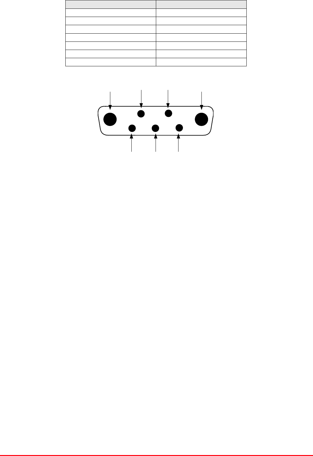
STTRS DOCUMENTATION
Document Number 80-330501HBKM – Issue A - Draft Page 321 of 500
Power Amplifier (12-018002) 7-Way Connector Pin-outs
Connector Pin Signal
A1 (large pin) +24V DC
A2 (large pin) GND
1 Alarm relay common
2 TTL alarm/0V good
3 Alarm relay contact (bad)
4 Alarm relay contact (good)
5 O/C good/0V bad (TTL)

STTRS DOCUMENTATION
Document Number 80-330501HBKM – Issue A - Draft Page 322 of 500
18.3.3. 800MHz Line Amplifier (55-165701)
5U rack mount case
800MHz Line Amplifier (55-165701) List of Major Components
Section Component
Part Component Part Description Qty Per
Assembly
18.3.3.3. 02-007206 Bandpass Filter 4
18.3.3.4. 07-015105 Wideband Asymmetric Coupler 1
18.3.3.5. 10-000901 Switched Attenuator 0.25W, 0 - 15dB 2
18.3.3.6. 11-006702 Low Noise Amplifier 1
18.3.3.7. 12-021901 Low Power Amplifier 2
17-001109* AGC Detector Assembly (Logarithmic) 1
17-001117* AGC Detector Assembly 1
18.3.3.8.
17-001201* AGC Attenuator Assembly 2
18.3.3.9. 80-008901 12V (Single) Relay Board 1
18.3.3.10. 94-100004 Dual Diode Assembly 1
18.3.3.11. 96-200047 DC/DC Converter 1
18.3.3.12. 96-300052 12V Switch-Mode PSU 1
*The sub components 17-001109, 17-001117 & 17-001201 are parts of the Automatic Gain Control
(AGC) system used in 800MHz Line Amplifier (55-165701); 17-001117 and 17-001201 are paired for
use in the uplink and 17-001109 and 17-001201 are paired for use in the down link
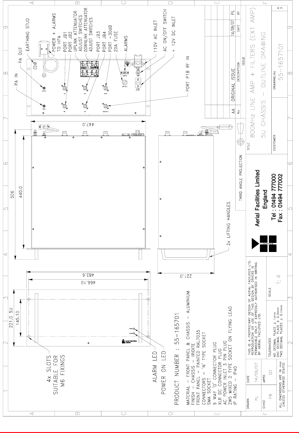
STTRS DOCUMENTATION
Document Number 80-330501HBKM – Issue A - Draft Page 323 of 500
18.3.3.1. 800MHz Line Amplifier (55-165701) Outline Drawing
Drawing number 55-1657101
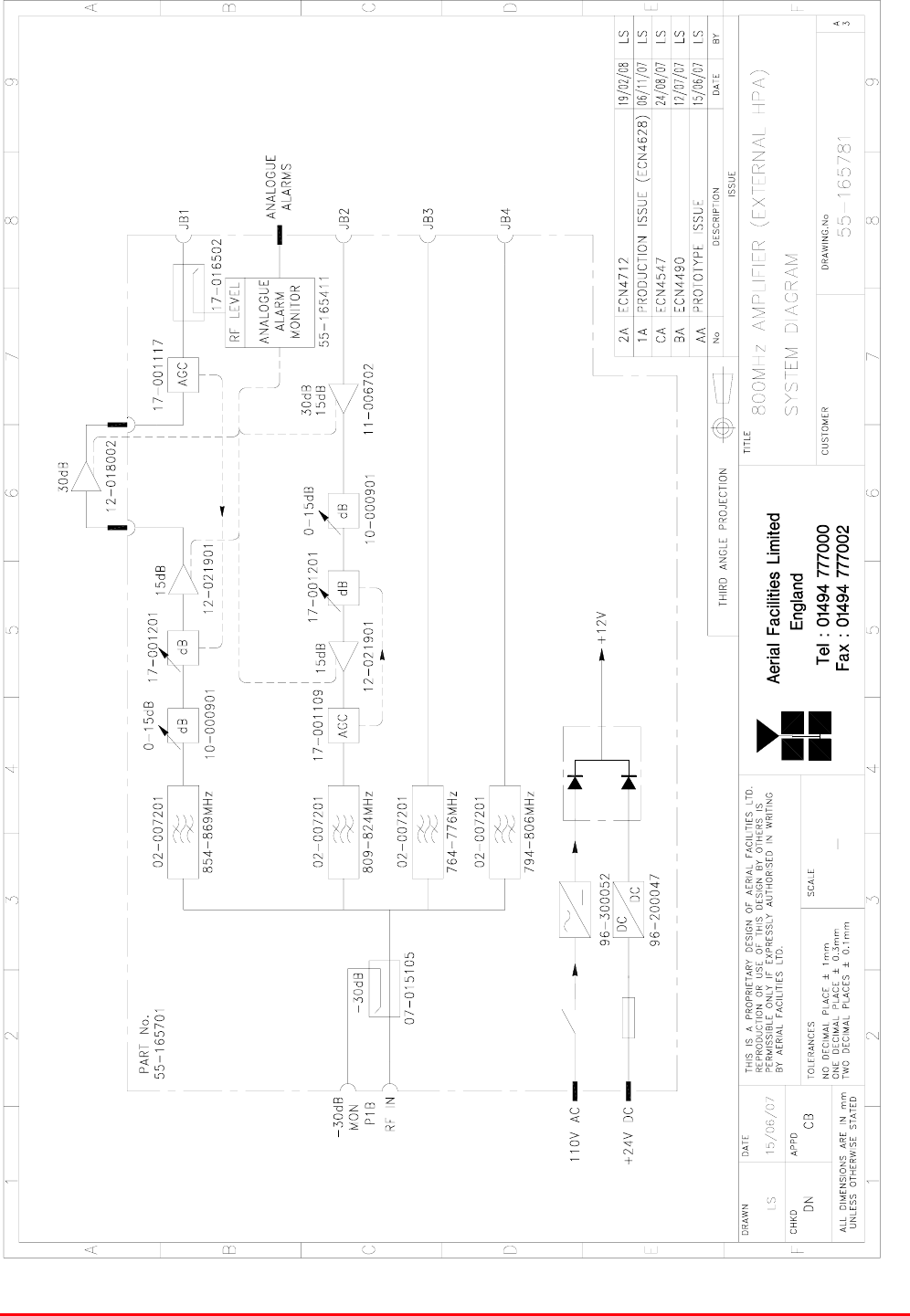
STTRS DOCUMENTATION
Document Number 80-330501HBKM – Issue A - Draft Page 324 of 500
18.3.3.2. 800MHz Line Amplifier (55-165701) System Diagram
Drawing number 55-165781
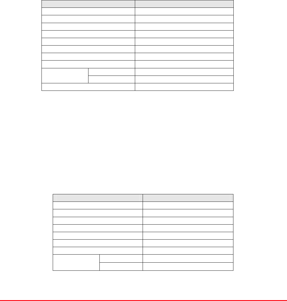
STTRS DOCUMENTATION
Document Number 80-330501HBKM – Issue A - Draft Page 325 of 500
18.3.3.3. Bandpass Filter (02-007206)
The bandpass filters are multi-section designs with a bandwidth dependent upon the passband
frequencies, (both tuned to customer requirements). The response shape is basically Chebyshev with
a passband design ripple of 0.1dB. The filters are of slot coupled, folded combline design, and are
carefully aligned during manufacture in order to optimise the insertion loss, VSWR and
intermodulation characteristics of the unit. The tuned elements are silver-plated to reduce surface
ohmic losses and maintain a good VSWR figure and 50Ω load at the input and output ports.
Being passive devices, the bandpass filters should have an extremely long operational life and require
no maintenance. Should a filter be suspect, it is usually most time efficient to replace the module
rather than attempt repair or re-tuning.
No adjustments should be attempted without full network sweep analysis facilities to monitor both
insertion loss and VSWR simultaneously.
02-007206 Specification
PARAMETER SPECIFICATION
Response type Chebyshev
Frequency range 800 - 950MHz *
Bandwidth 25MHz *
Number of sections 8
Insertion loss 1.2 dB
VSWR better than 1.2:1
Connectors SMA female
Power handling 100W max
operation -20°C to +60°C Temperature
range storage -40°C to +70°C
Weight 3 kg (typical) *tuned to Customer's specification
18.3.3.4. Wideband Asymmetric Coupler (07-015105)
The purpose of Wideband Asymmetric Coupler (07-015105) is to tap off a known portion (in this case
30dB) of RF signal from transmission lines and to combine them, for example through splitter units for
different purposes (alarms/monitoring etc.), whilst maintaining an accurate 50Ω load to all
ports/interfaces throughout the specified frequency range. They are known formally as directional
couplers as they couple power from the RF mainline in one direction only.
07-015105 Specification
PARAMETER SPECIFICATION
Construction Inductive air gap
Frequency 800-2500MHz
Through loss 0.4dB (typical)
Coupling level -30dB ±0.5dB
Isolation N/A
Weight <1.0kg
Connectors SMA, female
operation -20°C to +60°C
Temperature
range storage -40°C to +70°C

STTRS DOCUMENTATION
Document Number 80-330501HBKM – Issue A - Draft Page 326 of 500
18.3.3.5. Switched Attenuator 0.25W, 0 - 15dB (10-000901)
In many practical applications for Cell Enhancers etc., the gain in each path is found to be excessive.
Therefore, provision is made within the unit for the setting of attenuation in each path, to reduce the
gain.
10-000901 provides attenuation from 0 - 15dB in 2 dB steps The attenuation is simply set using the
four miniature toggle switches on the top of each unit. Each switch is clearly marked with the
attenuation it provides, and the total attenuation in line is the sum of the values switched in. They are
designed to maintain an accurate 50Ω impedance over their operating frequency at both input and
output.
10-000901 Specification
PARAMETER SPECIFICATION
Attenuation Values 0-15dB
Attenuation Steps 1, 2, 4 and 8dB
Power Handling 0.25 Watt
Attenuation Accuracy ± 1.0 dB
Frequency Range DC to 1GHz
Impedance 50Ω
Connectors SMA
VSWR 1.3:1
Weigh 0.2kg
operation -20°C to +60°C Temperature
range storage -40°C to +70°C
18.3.3.6. Low Noise Amplifier (11-006702)
The Gallium-Arsenide low noise amplifiers used in 800MHz Line Amplifier (55-165703) are double
stage, solid-state low noise amplifiers. Class A circuitry is used throughout the units to ensure
excellent linearity and extremely low noise over a very wide dynamic range. The active devices are
very moderately rated to provide a long trouble-free working life. There are no adjustments on these
amplifiers, and in the unlikely event of a failure, then the complete amplifier should be replaced. This
amplifier features its own in-built alarm system which gives a volt-free relay contact type alarm that is
easily integrated into the main alarm system.
11-006702 Specification
PARAMETER SPECIFICATION
Frequency range 800 – 1000MHz
Bandwidth <200MHz
Gain 29dB (typical)
1dB Compression point 20dBm
OIP3 33dBm
Input/Output return loss >18dB
Noise figure 1.3dB (typical)
Power consumption 180mA @ 24V DC
Supply voltage 10-24V DC
Connectors SMA female
operational -10°C to +60°C
Temperature range: storage -20°C to +70°C
Size 90 x 55 x 30.2mm
Weight 290gms (approximately)
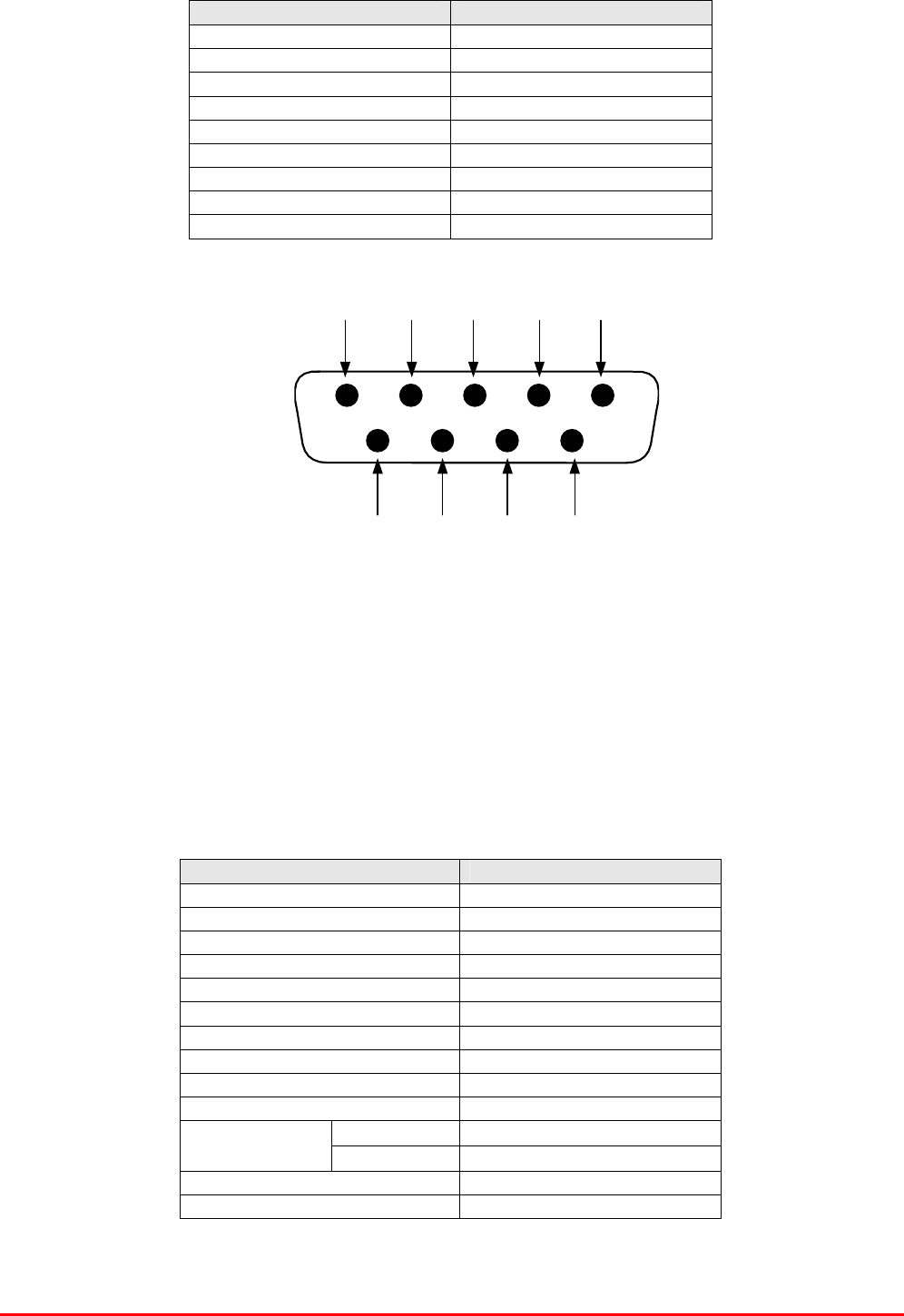
STTRS DOCUMENTATION
Document Number 80-330501HBKM – Issue A - Draft Page 327 of 500
7 8 96
1 2 3 4 5
9-Way Pin-Out Graphical Representation
Low Noise Amplifier (11-006702) ‘D’ Connector Pin-out details
Connector pin Signal
1 +Ve input (10-24V)
2 GND
3 Alarm RelayO/P bad
4 Alarm Relay common
5 Alarm Relay good
6 No connection
7 TTL voltage set
8 TTL alarm/0V (good)
9 O/C good/0V bad
18.3.3.7. Low Power Amplifier (12-021901)
The low power amplifier used is a triple stage solid-state low-noise amplifier. Class A circuitry is used
in the unit to ensure excellent linearity over a very wide dynamic range. The three active devices are
very moderately rated to provide a long trouble-free working life.
Its housing is an aluminium case (Iridite NCP finish) with SMA connectors for the RF input/output and
a D-Type connector for the power supply and the Current Fault Alarm Function.
There are no adjustments on this amplifier, and in the unlikely event of failure then the entire amplifier
should be replaced.
Low Power Amplifier (12-021901) Specification
PARAMETER SPECIFICATION
Frequency range 800-960MHz*
Bandwidth 20MHz *
Maximum RF output >1.0 Watt
Gain 15dB
1dB compression point +30.5dBm
3rd order intercept point +43dBm
Noise Figure <6dB
VSWR better than 1.5:1
Connectors SMA female
Supply 500mA @ 10-15V DC
operational -10°C to +60°C
Temperature
range storage -20°C to +70°C
Weight 0.5 kg
Size 167x52x25mm
* Tuned to Customer’s specification

STTRS DOCUMENTATION
Document Number 80-330501HBKM – Issue A - Draft Page 328 of 500
Low Power Amplifier (12-021901) 7-Way Connector Pin-outs
Connector Pin Signal
A1 (large pin) +24V DC
A2 (large pin) GND
1 Alarm relay common
2 TTL alarm/0V good
3 Alarm relay contact (bad)
4 Alarm relay contact (good)
5 O/C good/0V bad (TTL)
18.3.3.8. Automatic Gain Control
17-001109 AGC Detector Assembly (Logarithmic)
17-001117 AGC Detector Assembly
17-001201 AGC Attenuator Assembly
The sub components 17-001109, 17-001117 & 17-001201 are parts of the Automatic Gain Control
(AGC) system used in 800MHz Line Amplifier (55-165701); 17-001117 and 17-001201 are paired for
use in the uplink and 17-001109 and 17-001201 are paired for use in the downlink
800MHz Line Amplifier (55-165701) is fitted with two differing types of Automatic Gain Control (AGC)
system, one linear, and one logarithmic. The AGC with logarithmic detector (17-001117) is fitted in the
uplink path and the AGC with linear detector (17-001109) is fitted in the downlink path
The AFL Automatic Gain Control system consists of two units, a detector/amplifier and an attenuator.
The detector/amplifier unit is inserted in the RF path on the output of the power amplifier, and the
attenuator is situated in the RF path between the 1st and 2nd stages of amplification.
17-001117 and 17-001201 are paired for use in the uplink and 17-001109 and 17-001201 are paired
for use in the downlink
The attenuator comprises a 50Ω P.I.N diode, voltage-variable attenuator with a range of 3 to 30dB.
The attenuation is controlled by a DC voltage which is derived from the associated detector controller
board.

STTRS DOCUMENTATION
Document Number 80-330501HBKM – Issue A - Draft Page 329 of 500
Normally the attenuator is at minimum attenuation. The detector/amplifier unit monitors the RF level
being delivered by the power amplifier, and when a certain threshold is reached it begins to increase
the value of the attenuator to limit the RF output to the (factory set) threshold. Therefore overloading
of the power amplifier is avoided.
The factory set threshold is 1dB below the Enhancer 1dB compression point. Some adjustment of this
AGC threshold level is possible, a 10dB range is mostly achieved. It is not recommended under any
circumstances to adjust the AGC threshold to a level greater than the 1dB compression point as
system degradation will occur.
The detector comprises of a 50Ω transmission line with a resistive tap which samples a small portion
of the mainline power. The sampled signal is amplified and fed to a conventional half wave diode
rectifier, the output of which is a DC voltage proportional to the RF input signal.
This DC voltage is passed via an inverting DC amplifier with integrating characteristics, to the output,
which drives the attenuation control line of the corresponding AGC attenuator. This unit is fitted at
some earlier point in the RF circuit.
For small signals, below AGC onset, the output control line will be close to 12V and the AGC
attenuator will have minimum attenuation. As the signal level increases the control line voltage will
fall, increasing the attenuator value and keeping the system output level at a constant value.
AGC Specification (both types)
PARAMETER SPECIFICATION
Frequency range up to 1000MHz
Attenuation range 3 to 30dB
Attenuation steps continuously variable
VSWR better than 1.2:1
RF Connectors SMA female
attenuator 1W Power
handling detector/amp >30W (or as required)
operation -10°C to +60°C Temperature
range storage -20°C to +70°C
attenuator pcb 50 x 42 x 21mm
Size detector/amp pcb 54 x 42 x 21mm
attenuator 90grams
Weight detector/amp 100grams
18.3.3.9. 12V (Single) Relay Board (80-008901)
The General Purpose Relay Board allows the inversion of signals and the isolation of circuits. It is
equipped with a single dual pole change-over relay RL1, with completely isolated wiring, accessed
via a 15 way in-line connector.
The relay is provided with polarity protection diodes and diodes for suppressing the transients caused
by "flywheel effect" which can destroy switching transistors or induce spikes on neighbouring circuits.
It’s common use is to amalgamate all the alarm signals into one, volts-free relay contact pair for the
main alarm system.
STTRS DOCUMENTATION
Document Number 80-330501HBKM – Issue A - Draft Page 330 of 500
80-008901 Specification
PARAMETER SPECIFICATION
Operating voltage 8 to 30V (floating earth)
Alarm threshold Vcc - 1.20 volt +15%
Alarm output relay contacts
Max. switch current 1.0Amp
Max. switch volts 120Vdc/60VA
Max. switch power 24W/60VA
Min. switch load 10.0µA/10.0mV
Relay isolation 1.5kV
Mechanical life >2x10⁷ operations
Relay approval BT type 56
Connector details Screw terminals
operational -10°C to +60°C Temperature
range storage -20°C to +70°C
18.3.3.10. Dual Diode Assembly (94-100004)
The purpose of these dual diode assemblies is to allow two DC voltage sources to be combined, so
that the main DC rail within the equipment can be sourced from either a mains driven PSU, or
externally through an XLR connector or from dual mains driven PSUs. They are very heavy-duty
diodes and they prevent any reverse current from flowing back to their source or the alternative
supply rail. Combining diodes such as these will also be used if the equipment is to be powered from
external back-up batteries.
18.3.3.11. DC/DC Converter 96-200047
96-200047 is an O.E.M. high power device with a wide input range and 12.5 amp @ 12V (150Watts)
output capability used to derive a 12V fixed voltage power supply rail from a higher voltage supply, in
this case 12V. In the event of failure this unit should not be repaired, only replaced.
96-200047 Specification
PARAMETER SPECIFICATION
DC Input Voltage range 19 to 36V
DC Output voltage 12V ± 1%
Max. current load 12.5Amps
Operation -10°C to +60°C Temperature
range Storage -20°C to +85°C
Working Humidity 20 to 90% RHNC

STTRS DOCUMENTATION
Document Number 80-330501HBKM – Issue A - Draft Page 331 of 500
18.3.3.12. 12V Switch-Mode PSU (96-300052)
No routine maintenance of the PSU is required. If a fault is suspected, then the output voltage from
the power supply may be measured on its output terminals. This is typically set to 12.2V. The
adjustment potentiometer will be found close to the DC output terminals.
All the PSUs used in AFL Cell Enhancers are capable of operation from either 110 or 220V nominal
AC supplies. The line voltage is sensed automatically, so no adjustment or link setting is needed by
the operator.
96-300052 Specification
AC Input Supply 110 or 220V nominal
Voltage 85 - 265V AC (absolute limits)
Frequency 47 to 63Hz
DC Output Supply 12V DC (nominal)
Voltage 10.5-13.8V (absolute limits)
Current 12.5A

STTRS DOCUMENTATION
Document Number 80-330501HBKM – Issue A - Draft Page 332 of 500
18.3.4. 700MHz Line Amplifier (55-165702)
5U rack mount case
700MHz Line Amplifier (55-165702) List of Major Components
Section Component
Part Component Part Description Qty Per
Assembly
18.3.4.3. 02-007206 Bandpass Filter 4
18.3.4.4. 07-015105 Wideband Asymmetric Coupler 1
18.3.4.5. 10-000901 Switched Attenuator 0.25W, 0 - 15dB 2
18.3.4.6. 11-006702 Low Noise Amplifier 1
18.3.4.7. 12-021901 Low Power Amplifier 2
17-001109* AGC Detector Assembly (Logarithmic) 1
17-001117* AGC Detector Assembly 1
18.3.4.8.
17-001201* AGC Attenuator Assembly 2
18.3.4.9. 80-008901 12V (Single) Relay Board 1
18.3.4.0. 94-100004 Dual Diode Assembly 1
18.3.4.11. 96-200047 DC/DC Converter
18.3.4.12. 96-300052 12V Switch-Mode PSU 1
*The sub components 17-001109, 17-001117 & 17-001201 are parts of the Automatic Gain Control
(AGC) system used in 700MHz Line Amplifier (55-165702); 17-001117 and 17-001201 are paired for
use in the uplink and 17-001109 and 17-001201 are paired for use in the down link

STTRS DOCUMENTATION
Document Number 80-330501HBKM – Issue A - Draft Page 333 of 500
18.3.4.1. 700MHz Line Amplifier (55-165702) Outline Drawing
Drawing Number 55-1657102
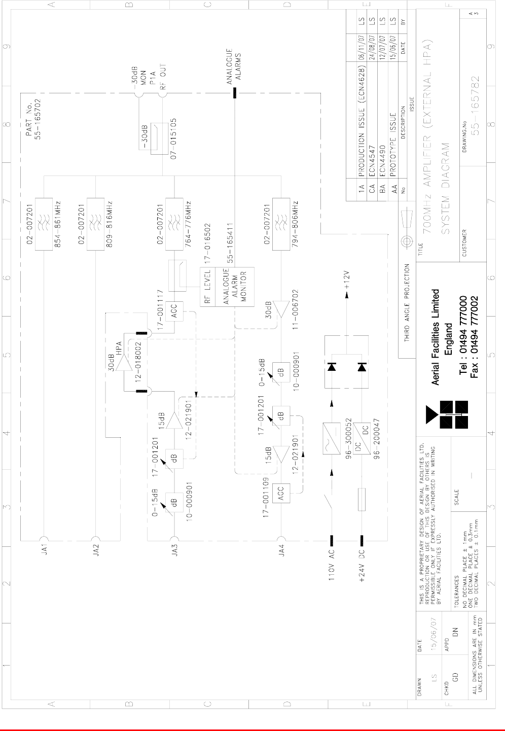
STTRS DOCUMENTATION
Document Number 80-330501HBKM – Issue A - Draft Page 334 of 500
18.3.4.2. 700MHz Line Amplifier (55-165702) System Diagram
Drawing Number 55-165782

STTRS DOCUMENTATION
Document Number 80-330501HBKM – Issue A - Draft Page 335 of 500
18.3.4.3. Bandpass Filter (02-007206)
The bandpass filters are multi-section designs with a bandwidth dependent upon the passband
frequencies, (both tuned to customer requirements). The response shape is basically Chebyshev with
a passband design ripple of 0.1dB. The filters are of slot coupled, folded combline design, and are
carefully aligned during manufacture in order to optimise the insertion loss, VSWR and
intermodulation characteristics of the unit. The tuned elements are silver-plated to reduce surface
ohmic losses and maintain a good VSWR figure and 50Ω load at the input and output ports.
Being passive devices, the bandpass filters should have an extremely long operational life and require
no maintenance. Should a filter be suspect, it is usually most time efficient to replace the module
rather than attempt repair or re-tuning.
No adjustments should be attempted without full network sweep analysis facilities to monitor both
insertion loss and VSWR simultaneously.
02-007206 Specification
PARAMETER SPECIFICATION
Response type Chebyshev
Frequency range 800 - 950MHz *
Bandwidth 25MHz *
Number of sections 8
Insertion loss 1.2 dB
VSWR better than 1.2:1
Connectors SMA female
Power handling 100W max
operation -20°C to +60°C Temperature
range storage -40°C to +70°C
Weight 3 kg (typical) *tuned to Customer's specification
18.3.4.4. Wideband Asymmetric Coupler (07-015105)
The purpose of Wideband Asymmetric Coupler (07-015105) is to tap off a known portion (in this case
30dB) of RF signal from transmission lines and to combine them, for example through splitter units for
different purposes (alarms/monitoring etc.), whilst maintaining an accurate 50Ω load to all
ports/interfaces throughout the specified frequency range. They are known formally as directional
couplers as they couple power from the RF mainline in one direction only.
07-015105 Specification
PARAMETER SPECIFICATION
Construction Inductive air gap
Frequency 800-2500MHz
Through loss 0.4dB (typical)
Coupling level -30dB ±0.5dB
Isolation N/A
Weight <1.0kg
Connectors SMA, female
operation -20°C to +60°C
Temperature
range storage -40°C to +70°C
STTRS DOCUMENTATION
Document Number 80-330501HBKM – Issue A - Draft Page 336 of 500
18.3.4.5. Switched Attenuator 0.25W, 0 - 15dB (10-000901)
In many practical applications for Cell Enhancers etc., the gain in each path is found to be excessive.
Therefore, provision is made within the unit for the setting of attenuation in each path, to reduce the
gain. 10-000901 provides attenuation from 0 - 15dB in 2 dB steps The attenuation is simply set using
the four miniature toggle switches on the top of each unit. Each switch is clearly marked with the
attenuation it provides, and the total attenuation in line is the sum of the values switched in. They are
designed to maintain an accurate 50Ω impedance over their operating frequency at both input and
output.
10-000901 Specification
PARAMETER SPECIFICATION
Attenuation Values 0-15dB
Attenuation Steps 1, 2, 4 and 8dB
Power Handling 0.25 Watt
Attenuation Accuracy ± 1.0 dB
Frequency Range DC to 1GHz
Impedance 50Ω
Connectors SMA
VSWR 1.3:1
Weigh 0.2kg
operation -20°C to +60°C Temperature
range storage -40°C to +70°C
18.3.4.6. Low Noise Amplifier (11-006702)
The Gallium-Arsenide low noise amplifiers used in 800MHz Line Amplifier (55-165703) are double
stage, solid-state low noise amplifiers. Class A circuitry is used throughout the units to ensure
excellent linearity and extremely low noise over a very wide dynamic range. The active devices are
very moderately rated to provide a long trouble-free working life. There are no adjustments on these
amplifiers, and in the unlikely event of a failure, then the complete amplifier should be replaced. This
amplifier features its own in-built alarm system which gives a volt-free relay contact type alarm that is
easily integrated into the main alarm system.
11-006702 Specification
PARAMETER SPECIFICATION
Frequency range 800 – 1000MHz
Bandwidth <200MHz
Gain 29dB (typical)
1dB Compression point 20dBm
OIP3 33dBm
Input/Output return loss >18dB
Noise figure 1.3dB (typical)
Power consumption 180mA @ 24V DC
Supply voltage 10-24V DC
Connectors SMA female
operational -10°C to +60°C
Temperature range: storage -20°C to +70°C
Size 90 x 55 x 30.2mm
Weight 290gms (approximately)

STTRS DOCUMENTATION
Document Number 80-330501HBKM – Issue A - Draft Page 337 of 500
7 8 96
1 2 3 4 5
9-Way Pin-Out Graphical Representation
Low Noise Amplifier (11-006702) ‘D’ Connector Pin-out details
Connector pin Signal
1 +Ve input (10-24V)
2 GND
3 Alarm RelayO/P bad
4 Alarm Relay common
5 Alarm Relay good
6 No connection
7 TTL voltage set
8 TTL alarm/0V (good)
9 O/C good/0V bad
18.3.4.7. Low Power Amplifier (12-021901)
The low power amplifier used is a triple stage solid-state low-noise amplifier. Class A circuitry is used
in the unit to ensure excellent linearity over a very wide dynamic range. The three active devices are
very moderately rated to provide a long trouble-free working life.
Its housing is an aluminium case (Iridite NCP finish) with SMA connectors for the RF input/output and
a D-Type connector for the power supply and the Current Fault Alarm Function.
There are no adjustments on this amplifier, and in the unlikely event of failure then the entire amplifier
should be replaced.
Low Power Amplifier (12-021901) Specification
PARAMETER SPECIFICATION
Frequency range 800-960MHz*
Bandwidth 20MHz *
Maximum RF output >1.0 Watt
Gain 15dB
1dB compression point +30.5dBm
3rd order intercept point +43dBm
Noise Figure <6dB
VSWR better than 1.5:1
Connectors SMA female
Supply 500mA @ 10-15V DC
operational -10°C to +60°C
Temperature
range storage -20°C to +70°C
Weight 0.5 kg
Size 167x52x25mm
* Tuned to Customer’s specification

STTRS DOCUMENTATION
Document Number 80-330501HBKM – Issue A - Draft Page 338 of 500
Low Power Amplifier (12-021901) 7-Way Connector Pin-outs
Connector Pin Signal
A1 (large pin) +24V DC
A2 (large pin) GND
1 Alarm relay common
2 TTL alarm/0V good
3 Alarm relay contact (bad)
4 Alarm relay contact (good)
5 O/C good/0V bad (TTL)
18.3.4.8. Automatic Gain Control
17-001109 AGC Detector Assembly (Logarithmic)
17-001117 AGC Detector Assembly
17-001201 AGC Attenuator Assembly
The sub components 17-001109, 17-001117 & 17-001201 are parts of the Automatic Gain Control
(AGC) system used in 700MHz Line Amplifier (55-165702); 17-001117 and 17-001201 are paired for
use in the uplink and 17-001109 and 17-001201 are paired for use in the downlink
700MHz Line Amplifier (55-165702) is fitted with two differing types of Automatic Gain Control (AGC)
system, one linear, and one logarithmic. The AGC with logarithmic detector (17-001117) is fitted in the
uplink path and the AGC with linear detector (17-001109) is fitted in the downlink path
The AFL Automatic Gain Control system consists of two units, a detector/amplifier and an attenuator.
The detector/amplifier unit is inserted in the RF path on the output of the power amplifier, and the
attenuator is situated in the RF path between the 1st and 2nd stages of amplification.
17-001117 and 17-001201 are paired for use in the uplink and 17-001109 and 17-001201 are paired
for use in the downlink
The attenuator comprises a 50Ω P.I.N diode, voltage-variable attenuator with a range of 3 to 30dB.
The attenuation is controlled by a DC voltage which is derived from the associated detector controller
board.

STTRS DOCUMENTATION
Document Number 80-330501HBKM – Issue A - Draft Page 339 of 500
Normally the attenuator is at minimum attenuation. The detector/amplifier unit monitors the RF level
being delivered by the power amplifier, and when a certain threshold is reached it begins to increase
the value of the attenuator to limit the RF output to the (factory set) threshold. Therefore overloading
of the power amplifier is avoided.
The factory set threshold is 1dB below the Enhancer 1dB compression point. Some adjustment of this
AGC threshold level is possible, a 10dB range is mostly achieved. It is not recommended under any
circumstances to adjust the AGC threshold to a level greater than the 1dB compression point as
system degradation will occur.
The detector comprises of a 50Ω transmission line with a resistive tap which samples a small portion
of the mainline power. The sampled signal is amplified and fed to a conventional half wave diode
rectifier, the output of which is a DC voltage proportional to the RF input signal.
This DC voltage is passed via an inverting DC amplifier with integrating characteristics, to the output,
which drives the attenuation control line of the corresponding AGC attenuator. This unit is fitted at
some earlier point in the RF circuit.
For small signals, below AGC onset, the output control line will be close to 12V and the AGC
attenuator will have minimum attenuation. As the signal level increases the control line voltage will
fall, increasing the attenuator value and keeping the system output level at a constant value.
AGC Specification (both types)
PARAMETER SPECIFICATION
Frequency range up to 1000MHz
Attenuation range 3 to 30dB
Attenuation steps continuously variable
VSWR better than 1.2:1
RF Connectors SMA female
attenuator 1W Power
handling detector/amp >30W (or as required)
operation -10°C to +60°C Temperature
range storage -20°C to +70°C
attenuator pcb 50 x 42 x 21mm
Size detector/amp pcb 54 x 42 x 21mm
attenuator 90grams
Weight detector/amp 100grams
18.3.4.9. 12V (Single) Relay Board (80-008901)
The General Purpose Relay Board allows the inversion of signals and the isolation of circuits. It is
equipped with a single dual pole change-over relay RL1, with completely isolated wiring, accessed
via a 15 way in-line connector.
The relay is provided with polarity protection diodes and diodes for suppressing the transients caused
by "flywheel effect" which can destroy switching transistors or induce spikes on neighbouring circuits.
It’s common use is to amalgamate all the alarm signals into one, volts-free relay contact pair for the
main alarm system.

STTRS DOCUMENTATION
Document Number 80-330501HBKM – Issue A - Draft Page 340 of 500
80-008901 Specification
PARAMETER SPECIFICATION
Operating voltage 8 to 30V (floating earth)
Alarm threshold Vcc - 1.20 volt +15%
Alarm output relay contacts
Max. switch current 1.0Amp
Max. switch volts 120Vdc/60VA
Max. switch power 24W/60VA
Min. switch load 10.0µA/10.0mV
Relay isolation 1.5kV
Mechanical life >2x10⁷ operations
Relay approval BT type 56
Connector details Screw terminals
operational -10°C to +60°C Temperature
range storage -20°C to +70°C
18.3.4.10. Dual Diode Assembly (94-100004)
The purpose of these dual diode assemblies is to allow two DC voltage sources to be combined, so
that the main DC rail within the equipment can be sourced from either a mains driven PSU, or
externally through an XLR connector or from dual mains driven PSUs. They are very heavy-duty
diodes and they prevent any reverse current from flowing back to their source or the alternative
supply rail. Combining diodes such as these will also be used if the equipment is to be powered from
external back-up batteries.
18.3.4.11. DC/DC Converter 96-200047
96-200047 is an O.E.M. high power device with a wide input range and 12.5 amp @ 12V (150Watts)
output capability used to derive a 12V fixed voltage power supply rail from a higher voltage supply, in
this case 12V. In the event of failure this unit should not be repaired, only replaced.
96-200047 Specification
PARAMETER SPECIFICATION
DC Input Voltage range 19 to 36V
DC Output voltage 12V ± 1%
Max. current load 12.5Amps
Operation -10°C to +60°C Temperature
range Storage -20°C to +85°C
Working Humidity 20 to 90% RHNC

STTRS DOCUMENTATION
Document Number 80-330501HBKM – Issue A - Draft Page 341 of 500
18.3.4.12. 12V Switch-Mode PSU (96-300052)
No routine maintenance of the PSU is required. If a fault is suspected, then the output voltage from
the power supply may be measured on its output terminals. This is typically set to 12.2V. The
adjustment potentiometer will be found close to the DC output terminals.
All the PSUs used in AFL Cell Enhancers are capable of operation from either 110 or 220V nominal
AC supplies. The line voltage is sensed automatically, so no adjustment or link setting is needed by
the operator.
96-300052 Specification
AC Input Supply 110 or 220V nominal
Voltage 85 - 265V AC (absolute limits)
Frequency 47 to 63Hz
DC Output Supply 12V DC (nominal)
Voltage 10.5-13.8V (absolute limits)
Current 12.5A

STTRS DOCUMENTATION
Document Number 80-330501HBKM – Issue A - Draft Page 342 of 500
19. UNIVERSITY STATION CROSS PASSAGE B (80-330590-2)
Wallmount case
number C06-CR-02
University Station Cross Passage B (80-330590-2)
Section Component
Part Component Part Description Qty Per
Assembly
19.3.1. 07-015102 Wideband Asymmetric Coupler 1
19.3.2. 12-018002 Power Amplifier 2
19.3.3. 55-165701 800MHz Line Amplifier 1
19.3.4. 55-165702 700MHz Line Amplifier 1
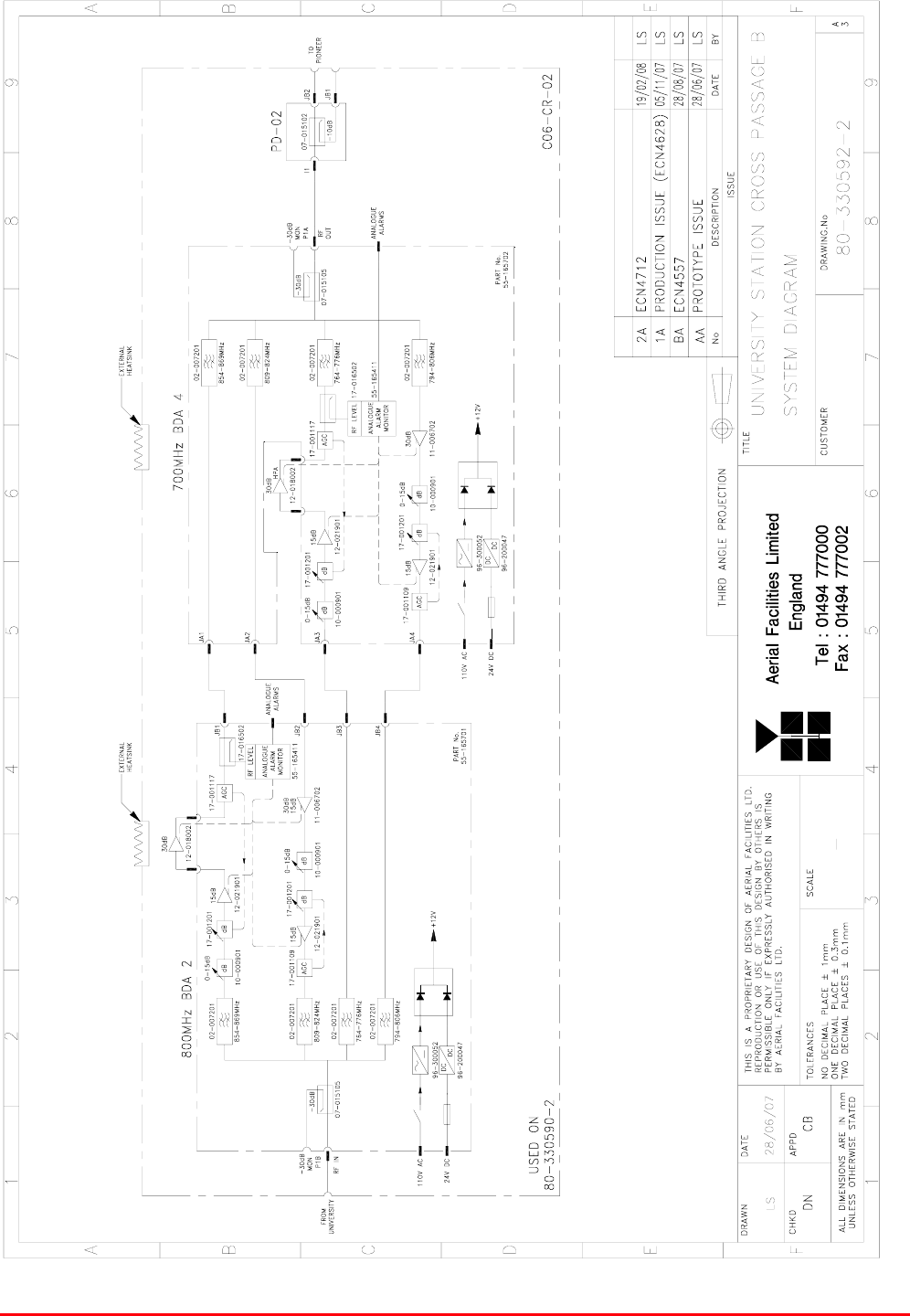
STTRS DOCUMENTATION
Document Number 80-330501HBKM – Issue A - Draft Page 343 of 500
19.1. University Station Cross Passage B (80-330590-2) System Diagram
Drawing number 80-330592-2
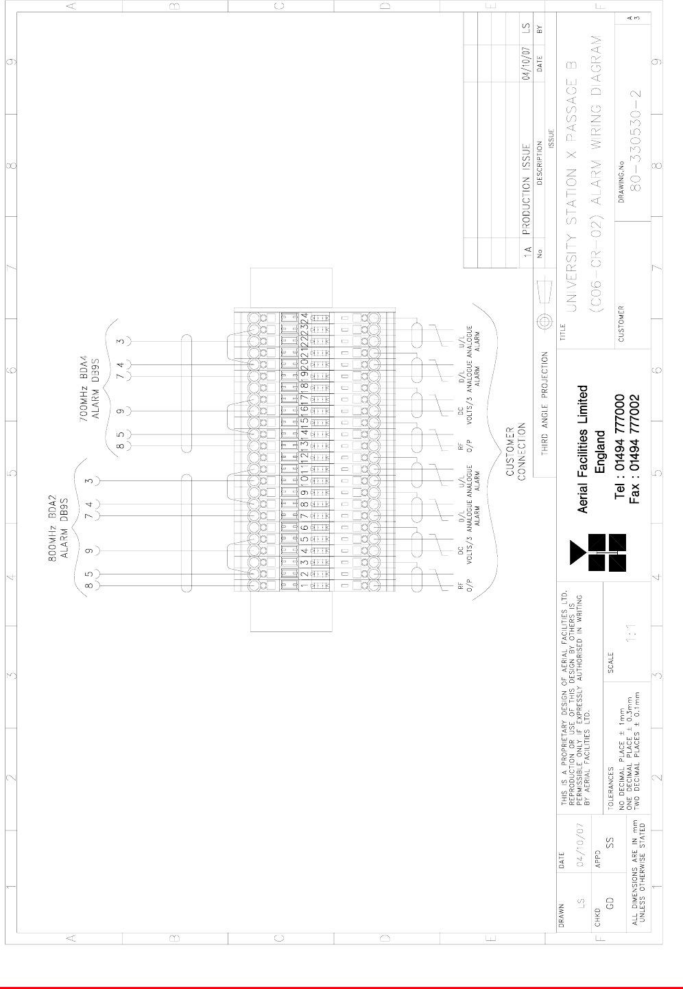
STTRS DOCUMENTATION
Document Number 80-330501HBKM – Issue A - Draft Page 344 of 500
19.2. University Station Cross Passage B (80-330590-2) Alarm Wiring Diagram
Drawing Number 80-330530-2
STTRS DOCUMENTATION
Document Number 80-330501HBKM – Issue A - Draft Page 345 of 500
19.3. University Station Cross Passage B (80-330590-2) Major Sub Components
19.3.1. Wideband Asymmetric Coupler (07-015102)
The purpose of Wideband Asymmetric Coupler (07-015102) is to tap off a known portion (in this case
10dB) of RF signal from transmission lines and to combine them, for example through splitter units for
different purposes (alarms/monitoring etc.), whilst maintaining an accurate 50Ω load to all
ports/interfaces throughout the specified frequency range. They are known formally as directional
couplers as they couple power from the RF mainline in one direction only.
07-015102 Specification
PARAMETER SPECIFICATION
Frequency Range 800 - 2500 MHz
Coupling Value 10 dB ± 1.0 dB
Main Line Insertion Loss <1.6 dB
VSWR 1.4:1
Directivity >18 dB
Power Rating 200 Watts
RF Connectors ‘N’ female
operation -20°C to +60°C
Temperature
range storage -40°C to +70°C
19.3.2. Power Amplifier (12-018002)
This amplifier is a Class A 20W power amplifier from 800-960MHz in a 1 stage balanced
configuration. It demonstrates a very high linearity and a very good input/output return loss (RL). It
has built in a Current Fault Alarm Function.
Its housing is an aluminium case (Iridite NCP finish) with SMA connectors for the RF input/output and
a D-Type connector for the power supply and the Current Fault Alarm Function.
12-018002 Specification
PARAMETER SPECIFICATION
Frequency range 800-960MHz
Small signal gain 30dB
Gain flatness ±1.2dB
I/O Return loss >18dB
1dB compression point 42.8dBm
OIP3 56dBm
Supply voltage 24V DC
Supply current 5.0Amps (Typical)
operational -10°C to +60°C Temperature
range storage -20°C to +70°C
Weight <2kg (no heatsink)

STTRS DOCUMENTATION
Document Number 80-330501HBKM – Issue A - Draft Page 346 of 500
Power Amplifier (12-018002) 7-Way Connector Pin-outs
Connector Pin Signal
A1 (large pin) +24V DC
A2 (large pin) GND
1 Alarm relay common
2 TTL alarm/0V good
3 Alarm relay contact (bad)
4 Alarm relay contact (good)
5 O/C good/0V bad (TTL)

STTRS DOCUMENTATION
Document Number 80-330501HBKM – Issue A - Draft Page 347 of 500
19.3.3. 800MHz Line Amplifier (55-165701)
5U rack mount case
800MHz Line Amplifier (55-165701) List of Major Components
Section Component
Part Component Part Description Qty Per
Assembly
19.3.3.3. 02-007206 Bandpass Filter 4
19.3.3.4. 07-015105 Wideband Asymmetric Coupler 1
19.3.3.5. 10-000901 Switched Attenuator 0.25W, 0 - 15dB 2
19.3.3.6. 11-006702 Low Noise Amplifier 1
19.3.3.7. 12-021901 Low Power Amplifier 2
17-001109 AGC Detector Assembly (Logarithmic) 1
17-001117 AGC Detector Assembly 1
19.3.3.8.
17-001201 AGC Attenuator Assembly 2
19.3.3.9. 80-008901 12V (Single) Relay Board 1
19.3.3.10. 94-100004 Dual Diode Assembly 1
19.3.3.11. 96-200047 DC/DC Converter 1
19.3.3.12. 96-300052 12V Switch-Mode PSU 1
*The sub components 17-001109, 17-001117 & 17-001201 are parts of the Automatic Gain Control
(AGC) system used in 800MHz Line Amplifier (55-165701); 17-001117 and 17-001201 are paired for
use in the uplink and 17-001109 and 17-001201 are paired for use in the down link
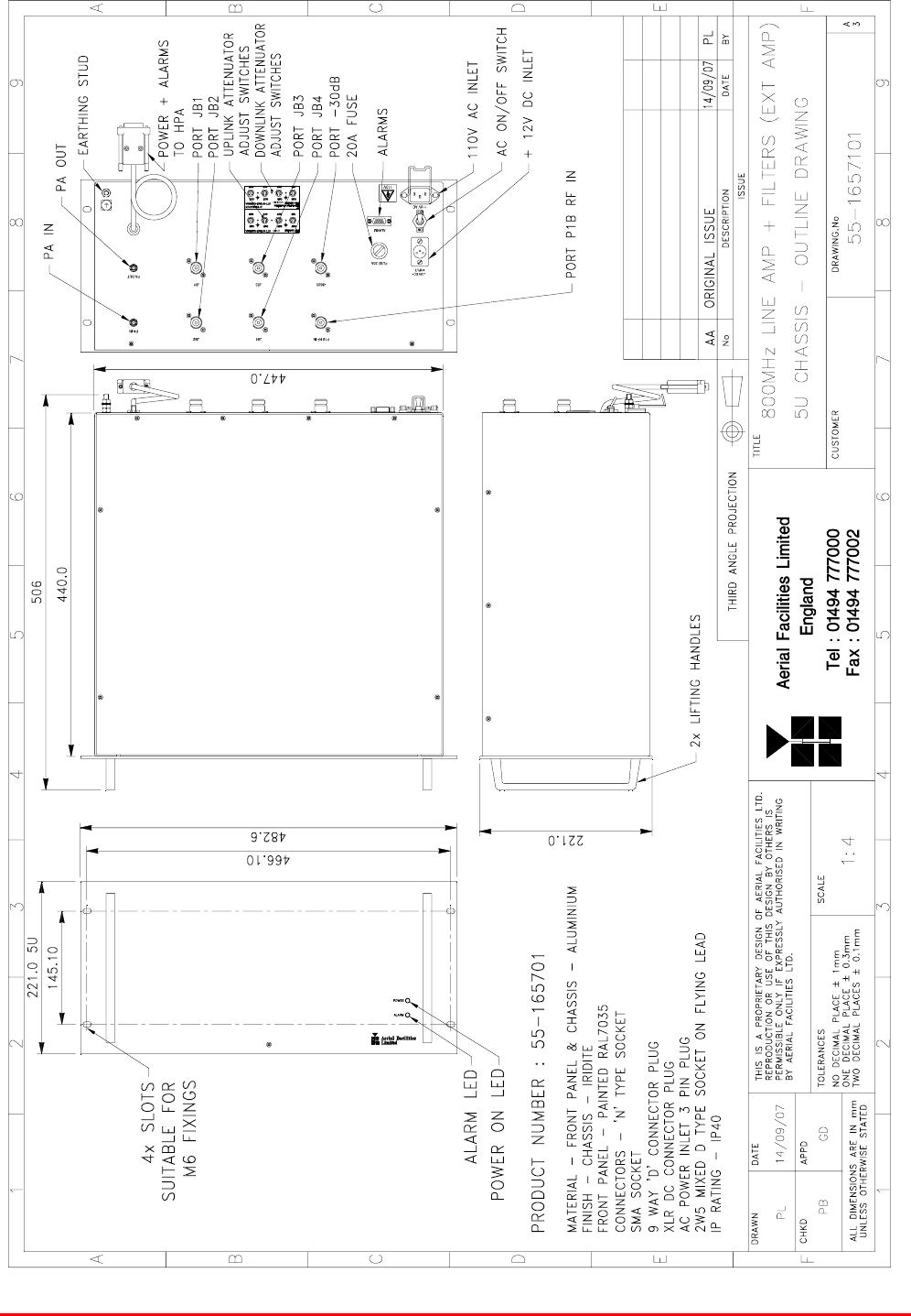
STTRS DOCUMENTATION
Document Number 80-330501HBKM – Issue A - Draft Page 348 of 500
19.3.3.1. 800MHz Line Amplifier (55-165701) Outline Drawing
Drawing number 55-1657101
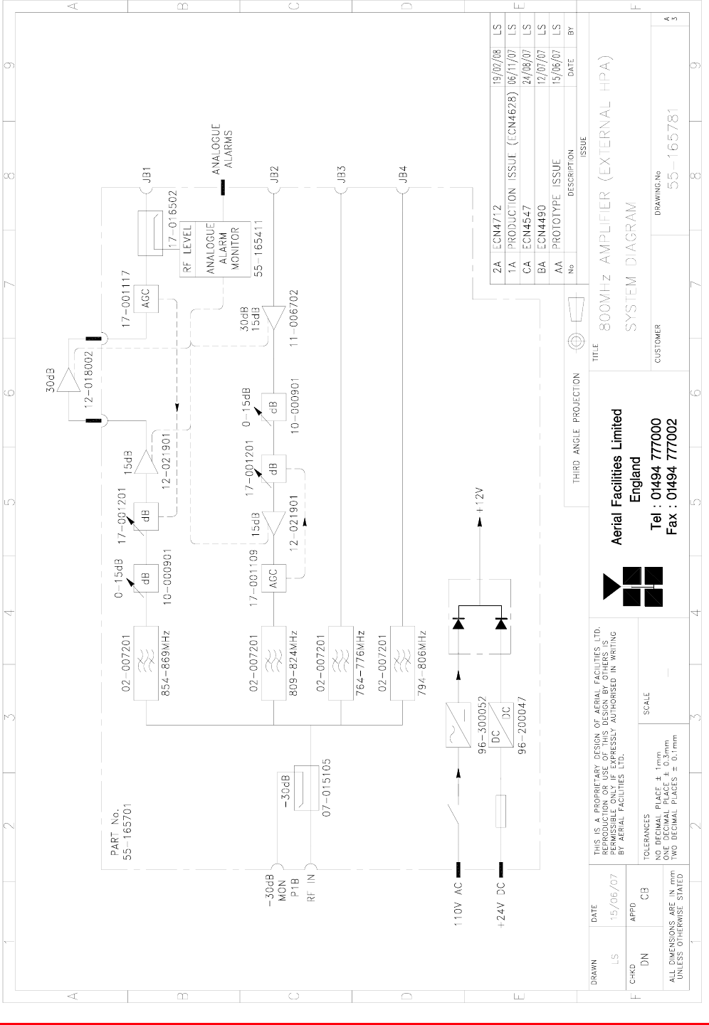
STTRS DOCUMENTATION
Document Number 80-330501HBKM – Issue A - Draft Page 349 of 500
19.3.3.2. 800MHz Line Amplifier (55-165701) System Diagram
Drawing number 55-165781
STTRS DOCUMENTATION
Document Number 80-330501HBKM – Issue A - Draft Page 350 of 500
19.3.3.3. Bandpass Filter (02-007206)
The bandpass filters are multi-section designs with a bandwidth dependent upon the passband
frequencies, (both tuned to customer requirements). The response shape is basically Chebyshev with
a passband design ripple of 0.1dB. The filters are of slot coupled, folded combline design, and are
carefully aligned during manufacture in order to optimise the insertion loss, VSWR and
intermodulation characteristics of the unit. The tuned elements are silver-plated to reduce surface
ohmic losses and maintain a good VSWR figure and 50Ω load at the input and output ports.
Being passive devices, the bandpass filters should have an extremely long operational life and require
no maintenance. Should a filter be suspect, it is usually most time efficient to replace the module
rather than attempt repair or re-tuning.
No adjustments should be attempted without full network sweep analysis facilities to monitor both
insertion loss and VSWR simultaneously.
02-007206 Specification
PARAMETER SPECIFICATION
Response type Chebyshev
Frequency range 800 - 950MHz *
Bandwidth 25MHz *
Number of sections 8
Insertion loss 1.2 dB
VSWR better than 1.2:1
Connectors SMA female
Power handling 100W max
operation -20°C to +60°C Temperature
range storage -40°C to +70°C
Weight 3 kg (typical) *tuned to Customer's specification
19.3.3.4. Wideband Asymmetric Coupler (07-015105)
The purpose of Wideband Asymmetric Coupler (07-015105) is to tap off a known portion (in this case
30dB) of RF signal from transmission lines and to combine them, for example through splitter units for
different purposes (alarms/monitoring etc.), whilst maintaining an accurate 50Ω load to all
ports/interfaces throughout the specified frequency range. They are known formally as directional
couplers as they couple power from the RF mainline in one direction only.
07-015105 Specification
PARAMETER SPECIFICATION
Construction Inductive air gap
Frequency 800-2500MHz
Through loss 0.4dB (typical)
Coupling level -30dB ±0.5dB
Isolation N/A
Weight <1.0kg
Connectors SMA, female
operation -20°C to +60°C
Temperature
range storage -40°C to +70°C

STTRS DOCUMENTATION
Document Number 80-330501HBKM – Issue A - Draft Page 351 of 500
19.3.3.5. Switched Attenuator 0.25W, 0 - 15dB (10-000901)
In many practical applications for Cell Enhancers etc., the gain in each path is found to be excessive.
Therefore, provision is made within the unit for the setting of attenuation in each path, to reduce the
gain.
10-000901 provides attenuation from 0 - 15dB in 2 dB steps The attenuation is simply set using the
four miniature toggle switches on the top of each unit. Each switch is clearly marked with the
attenuation it provides, and the total attenuation in line is the sum of the values switched in. They are
designed to maintain an accurate 50Ω impedance over their operating frequency at both input and
output.
10-000901 Specification
PARAMETER SPECIFICATION
Attenuation Values 0-15dB
Attenuation Steps 1, 2, 4 and 8dB
Power Handling 0.25 Watt
Attenuation Accuracy ± 1.0 dB
Frequency Range DC to 1GHz
Impedance 50Ω
Connectors SMA
VSWR 1.3:1
Weigh 0.2kg
operation -20°C to +60°C Temperature
range storage -40°C to +70°C
19.3.3.6. Low Noise Amplifier (11-006702)
The Gallium-Arsenide low noise amplifiers used in 800MHz Line Amplifier (55-165703) are double
stage, solid-state low noise amplifiers. Class A circuitry is used throughout the units to ensure
excellent linearity and extremely low noise over a very wide dynamic range. The active devices are
very moderately rated to provide a long trouble-free working life. There are no adjustments on these
amplifiers, and in the unlikely event of a failure, then the complete amplifier should be replaced. This
amplifier features its own in-built alarm system which gives a volt-free relay contact type alarm that is
easily integrated into the main alarm system.
11-006702 Specification
PARAMETER SPECIFICATION
Frequency range 800 – 1000MHz
Bandwidth <200MHz
Gain 29dB (typical)
1dB Compression point 20dBm
OIP3 33dBm
Input/Output return loss >18dB
Noise figure 1.3dB (typical)
Power consumption 180mA @ 24V DC
Supply voltage 10-24V DC
Connectors SMA female
operational -10°C to +60°C
Temperature range: storage -20°C to +70°C
Size 90 x 55 x 30.2mm
Weight 290gms (approximately)

STTRS DOCUMENTATION
Document Number 80-330501HBKM – Issue A - Draft Page 352 of 500
7 8 96
1 2 3 4 5
9-Way Pin-Out Graphical Representation
Low Noise Amplifier (11-006702) ‘D’ Connector Pin-out details
Connector pin Signal
1 +Ve input (10-24V)
2 GND
3 Alarm RelayO/P bad
4 Alarm Relay common
5 Alarm Relay good
6 No connection
7 TTL voltage set
8 TTL alarm/0V (good)
9 O/C good/0V bad
19.3.3.7. Low Power Amplifier (12-021901)
The low power amplifier used is a triple stage solid-state low-noise amplifier. Class A circuitry is used
in the unit to ensure excellent linearity over a very wide dynamic range. The three active devices are
very moderately rated to provide a long trouble-free working life.
Its housing is an aluminium case (Iridite NCP finish) with SMA connectors for the RF input/output and
a D-Type connector for the power supply and the Current Fault Alarm Function.
There are no adjustments on this amplifier, and in the unlikely event of failure then the entire amplifier
should be replaced.
Low Power Amplifier (12-021901) Specification
PARAMETER SPECIFICATION
Frequency range 800-960MHz*
Bandwidth 20MHz *
Maximum RF output >1.0 Watt
Gain 15dB
1dB compression point +30.5dBm
3rd order intercept point +43dBm
Noise Figure <6dB
VSWR better than 1.5:1
Connectors SMA female
Supply 500mA @ 10-15V DC
operational -10°C to +60°C
Temperature
range storage -20°C to +70°C
Weight 0.5 kg
Size 167x52x25mm
* Tuned to Customer’s specification

STTRS DOCUMENTATION
Document Number 80-330501HBKM – Issue A - Draft Page 353 of 500
Low Power Amplifier (12-021901) 7-Way Connector Pin-outs
Connector Pin Signal
A1 (large pin) +24V DC
A2 (large pin) GND
1 Alarm relay common
2 TTL alarm/0V good
3 Alarm relay contact (bad)
4 Alarm relay contact (good)
5 O/C good/0V bad (TTL)
19.3.3.8. Automatic Gain Control
17-001109 AGC Detector Assembly (Logarithmic)
17-001117 AGC Detector Assembly
17-001201 AGC Attenuator Assembly
The sub components 17-001109, 17-001117 & 17-001201 are parts of the Automatic Gain Control
(AGC) system used in 800MHz Line Amplifier (55-165701); 17-001117 and 17-001201 are paired for
use in the uplink and 17-001109 and 17-001201 are paired for use in the downlink
800MHz Line Amplifier (55-165701) is fitted with two differing types of Automatic Gain Control (AGC)
system, one linear, and one logarithmic. The AGC with logarithmic detector (17-001117) is fitted in the
uplink path and the AGC with linear detector (17-001109) is fitted in the downlink path
The AFL Automatic Gain Control system consists of two units, a detector/amplifier and an attenuator.
The detector/amplifier unit is inserted in the RF path on the output of the power amplifier, and the
attenuator is situated in the RF path between the 1st and 2nd stages of amplification.
17-001117 and 17-001201 are paired for use in the uplink and 17-001109 and 17-001201 are paired
for use in the downlink
The attenuator comprises a 50Ω P.I.N diode, voltage-variable attenuator with a range of 3 to 30dB.
The attenuation is controlled by a DC voltage which is derived from the associated detector controller
board.

STTRS DOCUMENTATION
Document Number 80-330501HBKM – Issue A - Draft Page 354 of 500
Normally the attenuator is at minimum attenuation. The detector/amplifier unit monitors the RF level
being delivered by the power amplifier, and when a certain threshold is reached it begins to increase
the value of the attenuator to limit the RF output to the (factory set) threshold. Therefore overloading
of the power amplifier is avoided.
The factory set threshold is 1dB below the Enhancer 1dB compression point. Some adjustment of this
AGC threshold level is possible, a 10dB range is mostly achieved. It is not recommended under any
circumstances to adjust the AGC threshold to a level greater than the 1dB compression point as
system degradation will occur.
The detector comprises of a 50Ω transmission line with a resistive tap which samples a small portion
of the mainline power. The sampled signal is amplified and fed to a conventional half wave diode
rectifier, the output of which is a DC voltage proportional to the RF input signal.
This DC voltage is passed via an inverting DC amplifier with integrating characteristics, to the output,
which drives the attenuation control line of the corresponding AGC attenuator. This unit is fitted at
some earlier point in the RF circuit.
For small signals, below AGC onset, the output control line will be close to 12V and the AGC
attenuator will have minimum attenuation. As the signal level increases the control line voltage will
fall, increasing the attenuator value and keeping the system output level at a constant value.
AGC Specification (both types)
PARAMETER SPECIFICATION
Frequency range up to 1000MHz
Attenuation range 3 to 30dB
Attenuation steps continuously variable
VSWR better than 1.2:1
RF Connectors SMA female
attenuator 1W Power
handling detector/amp >30W (or as required)
operation -10°C to +60°C Temperature
range storage -20°C to +70°C
attenuator pcb 50 x 42 x 21mm
Size detector/amp pcb 54 x 42 x 21mm
attenuator 90grams
Weight detector/amp 100grams
19.3.3.9. 12V (Single) Relay Board (80-008901)
The General Purpose Relay Board allows the inversion of signals and the isolation of circuits. It is
equipped with a single dual pole change-over relay RL1, with completely isolated wiring, accessed
via a 15 way in-line connector.
The relay is provided with polarity protection diodes and diodes for suppressing the transients caused
by "flywheel effect" which can destroy switching transistors or induce spikes on neighbouring circuits.
It’s common use is to amalgamate all the alarm signals into one, volts-free relay contact pair for the
main alarm system.
STTRS DOCUMENTATION
Document Number 80-330501HBKM – Issue A - Draft Page 355 of 500
80-008901 Specification
PARAMETER SPECIFICATION
Operating voltage 8 to 30V (floating earth)
Alarm threshold Vcc - 1.20 volt +15%
Alarm output relay contacts
Max. switch current 1.0Amp
Max. switch volts 120Vdc/60VA
Max. switch power 24W/60VA
Min. switch load 10.0µA/10.0mV
Relay isolation 1.5kV
Mechanical life >2x10⁷ operations
Relay approval BT type 56
Connector details Screw terminals
operational -10°C to +60°C Temperature
range storage -20°C to +70°C
19.3.3.10. Dual Diode Assembly (94-100004)
The purpose of these dual diode assemblies is to allow two DC voltage sources to be combined, so
that the main DC rail within the equipment can be sourced from either a mains driven PSU, or
externally through an XLR connector or from dual mains driven PSUs. They are very heavy-duty
diodes and they prevent any reverse current from flowing back to their source or the alternative
supply rail. Combining diodes such as these will also be used if the equipment is to be powered from
external back-up batteries.
19.3.3.11. DC/DC Converter 96-200047
96-200047 is an O.E.M. high power device with a wide input range and 12.5 amp @ 12V (150Watts)
output capability used to derive a 12V fixed voltage power supply rail from a higher voltage supply, in
this case 12V. In the event of failure this unit should not be repaired, only replaced.
96-200047 Specification
PARAMETER SPECIFICATION
DC Input Voltage range 19 to 36V
DC Output voltage 12V ± 1%
Max. current load 12.5Amps
Operation -10°C to +60°C Temperature
range Storage -20°C to +85°C
Working Humidity 20 to 90% RHNC

STTRS DOCUMENTATION
Document Number 80-330501HBKM – Issue A - Draft Page 356 of 500
19.3.3.12. 12V Switch-Mode PSU (96-300052)
No routine maintenance of the PSU is required. If a fault is suspected, then the output voltage from
the power supply may be measured on its output terminals. This is typically set to 12.2V. The
adjustment potentiometer will be found close to the DC output terminals.
All the PSUs used in AFL Cell Enhancers are capable of operation from either 110 or 220V nominal
AC supplies. The line voltage is sensed automatically, so no adjustment or link setting is needed by
the operator.
96-300052 Specification
AC Input Supply 110 or 220V nominal
Voltage 85 - 265V AC (absolute limits)
Frequency 47 to 63Hz
DC Output Supply 12V DC (nominal)
Voltage 10.5-13.8V (absolute limits)
Current 12.5A

STTRS DOCUMENTATION
Document Number 80-330501HBKM – Issue A - Draft Page 357 of 500
19.3.4. 700MHz Line Amplifier (55-165702)
5U rack mount case
700MHz Line Amplifier (55-165702) List of Major Components
Section Component
Part Component Part Description Qty Per
Assembly
19.3.4.3. 02-007206 900MHZ 8POLE 25MHz+ B/W "SMA" 4
19.3.4.4. 07-015105 ASYMMETRIC CPLR 30dB 800-2500MHz GA 1
19.3.4.5. 10-000901 SW ATT 0-15dB 0.25W SMA F 2
19.3.4.6. 11-006702 800-1000MHz LNA 29dB (cw RELAY) KIT 1
19.3.4.7. 12-021901 Low Power Amplifier 2
17-001109* AGC Detector Assembly (Logarithmic) 1
17-001117* AGC Detector Assembly 1
19.3.4.8.
17-001201* AGC Attenuator Assembly 2
19.3.4.9. 80-008901 12V RELAY PCB ASSEMBLY 1
19.3.4.10. 94-100004 STPS12045TV 60A DUAL DIODE 1
19.3.4.11. 96-200047 DC/DC Converter 1
19.3.4.12. 96-300052 JWS150-12/A PSU (COUTANT LAMBDA) 1
*The sub components 17-001109, 17-001117 & 17-001201 are parts of the Automatic Gain Control
(AGC) system used in 700MHz Line Amplifier (55-165702); 17-001117 and 17-001201 are paired for
use in the uplink and 17-001109 and 17-001201 are paired for use in the downlink
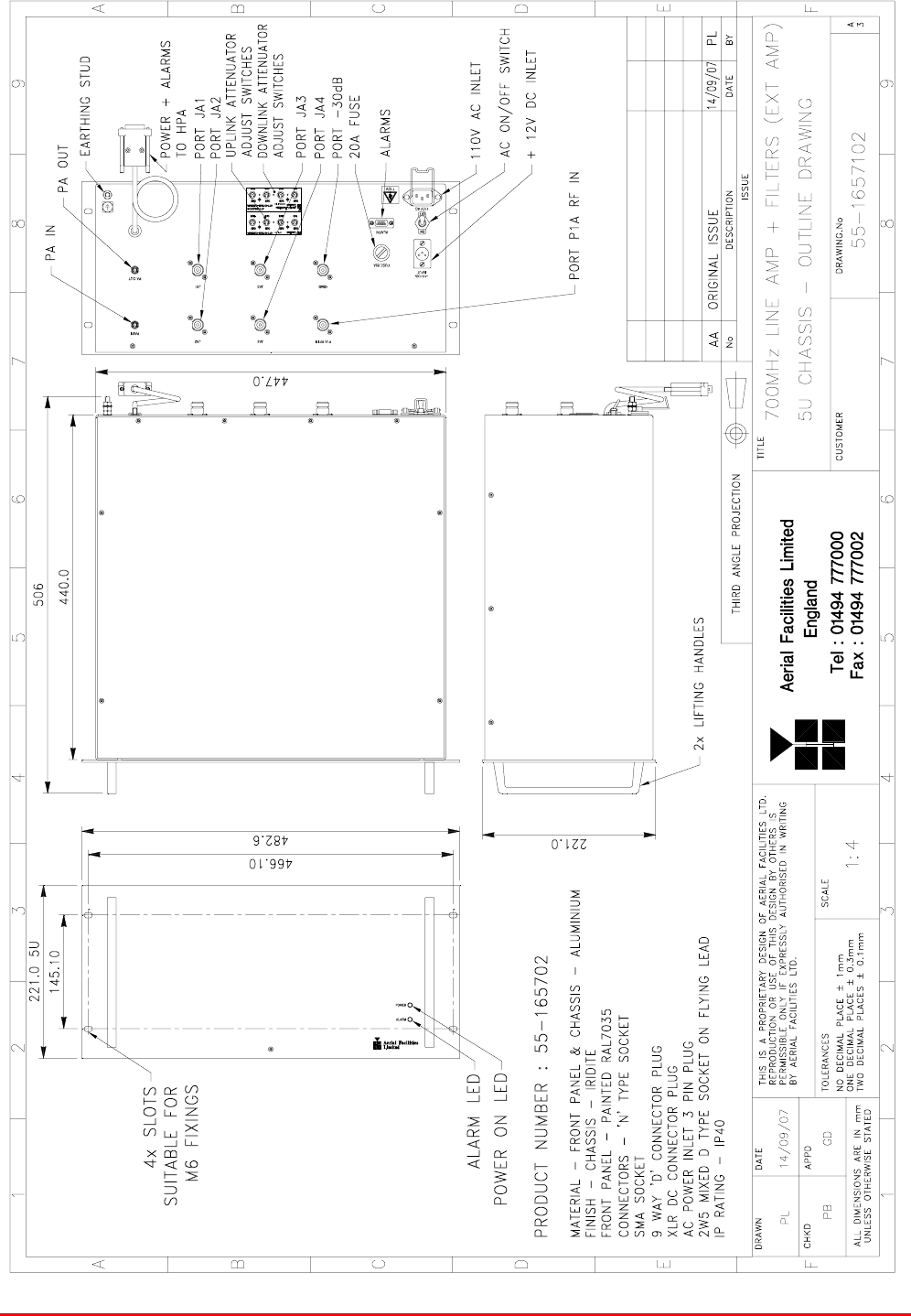
STTRS DOCUMENTATION
Document Number 80-330501HBKM – Issue A - Draft Page 358 of 500
19.3.4.1. 700MHz Line Amplifier (55-165702) Outline Drawing
Drawing Number 55-1657102
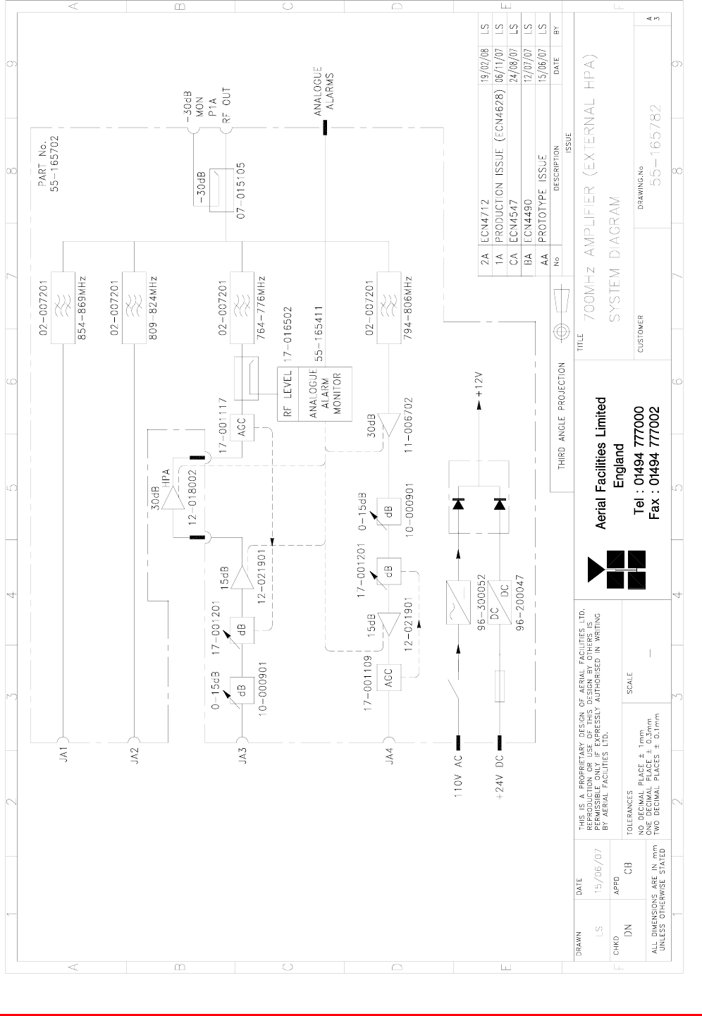
STTRS DOCUMENTATION
Document Number 80-330501HBKM – Issue A - Draft Page 359 of 500
19.3.4.2. 700MHz Line Amplifier (55-165702) System Diagram
Drawing Number 55-165782
STTRS DOCUMENTATION
Document Number 80-330501HBKM – Issue A - Draft Page 360 of 500
19.3.4.3. Bandpass Filter (02-007206)
The bandpass filters are multi-section designs with a bandwidth dependent upon the passband
frequencies, (both tuned to customer requirements). The response shape is basically Chebyshev with
a passband design ripple of 0.1dB. The filters are of slot coupled, folded combline design, and are
carefully aligned during manufacture in order to optimise the insertion loss, VSWR and
intermodulation characteristics of the unit. The tuned elements are silver-plated to reduce surface
ohmic losses and maintain a good VSWR figure and 50Ω load at the input and output ports.
Being passive devices, the bandpass filters should have an extremely long operational life and require
no maintenance. Should a filter be suspect, it is usually most time efficient to replace the module
rather than attempt repair or re-tuning.
No adjustments should be attempted without full network sweep analysis facilities to monitor both
insertion loss and VSWR simultaneously.
02-007206 Specification
PARAMETER SPECIFICATION
Response type Chebyshev
Frequency range 800 - 950MHz *
Bandwidth 25MHz *
Number of sections 8
Insertion loss 1.2 dB
VSWR better than 1.2:1
Connectors SMA female
Power handling 100W max
operation -20°C to +60°C Temperature
range storage -40°C to +70°C
Weight 3 kg (typical) *tuned to Customer's specification
19.3.4.4. Wideband Asymmetric Coupler (07-015105)
The purpose of Wideband Asymmetric Coupler (07-015105) is to tap off a known portion (in this case
30dB) of RF signal from transmission lines and to combine them, for example through splitter units for
different purposes (alarms/monitoring etc.), whilst maintaining an accurate 50Ω load to all
ports/interfaces throughout the specified frequency range. They are known formally as directional
couplers as they couple power from the RF mainline in one direction only.
07-015105 Specification
PARAMETER SPECIFICATION
Construction Inductive air gap
Frequency 800-2500MHz
Through loss 0.4dB (typical)
Coupling level -30dB ±0.5dB
Isolation N/A
Weight <1.0kg
Connectors SMA, female
operation -20°C to +60°C
Temperature
range storage -40°C to +70°C

STTRS DOCUMENTATION
Document Number 80-330501HBKM – Issue A - Draft Page 361 of 500
19.3.4.5. Switched Attenuator 0.25W, 0 - 15dB (10-000901)
In many practical applications for Cell Enhancers etc., the gain in each path is found to be excessive.
Therefore, provision is made within the unit for the setting of attenuation in each path, to reduce the
gain.
10-000901 provides attenuation from 0 - 15dB in 2 dB steps The attenuation is simply set using the
four miniature toggle switches on the top of each unit. Each switch is clearly marked with the
attenuation it provides, and the total attenuation in line is the sum of the values switched in. They are
designed to maintain an accurate 50Ω impedance over their operating frequency at both input and
output.
10-000901 Specification
PARAMETER SPECIFICATION
Attenuation Values 0-15dB
Attenuation Steps 1, 2, 4 and 8dB
Power Handling 0.25 Watt
Attenuation Accuracy ± 1.0 dB
Frequency Range DC to 1GHz
Impedance 50Ω
Connectors SMA
VSWR 1.3:1
Weigh 0.2kg
operation -20°C to +60°C Temperature
range storage -40°C to +70°C
19.3.4.6. Low Noise Amplifier (11-006702)
The Gallium-Arsenide low noise amplifiers used in 800MHz Line Amplifier (55-165703) are double
stage, solid-state low noise amplifiers. Class A circuitry is used throughout the units to ensure
excellent linearity and extremely low noise over a very wide dynamic range. The active devices are
very moderately rated to provide a long trouble-free working life. There are no adjustments on these
amplifiers, and in the unlikely event of a failure, then the complete amplifier should be replaced. This
amplifier features its own in-built alarm system which gives a volt-free relay contact type alarm that is
easily integrated into the main alarm system.
11-006702 Specification
PARAMETER SPECIFICATION
Frequency range 800 – 1000MHz
Bandwidth <200MHz
Gain 29dB (typical)
1dB Compression point 20dBm
OIP3 33dBm
Input/Output return loss >18dB
Noise figure 1.3dB (typical)
Power consumption 180mA @ 24V DC
Supply voltage 10-24V DC
Connectors SMA female
operational -10°C to +60°C
Temperature range: storage -20°C to +70°C
Size 90 x 55 x 30.2mm
Weight 290gms (approximately)
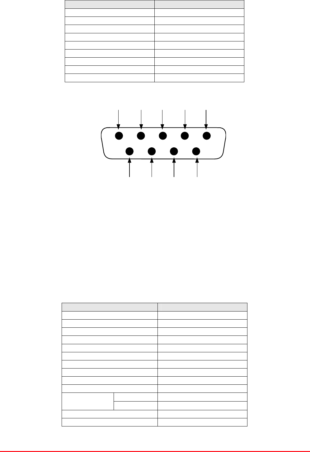
STTRS DOCUMENTATION
Document Number 80-330501HBKM – Issue A - Draft Page 362 of 500
7 8 96
1 2 3 4 5
9-Way Pin-Out Graphical Representation
Low Noise Amplifier (11-006702) ‘D’ Connector Pin-out details
Connector pin Signal
1 +Ve input (10-24V)
2 GND
3 Alarm RelayO/P bad
4 Alarm Relay common
5 Alarm Relay good
6 No connection
7 TTL voltage set
8 TTL alarm/0V (good)
9 O/C good/0V bad
19.3.4.7. Low Power Amplifier (12-021901)
The low power amplifier used is a triple stage solid-state low-noise amplifier. Class A circuitry is used
in the unit to ensure excellent linearity over a very wide dynamic range. The three active devices are
very moderately rated to provide a long trouble-free working life.
Its housing is an aluminium case (Iridite NCP finish) with SMA connectors for the RF input/output and
a D-Type connector for the power supply and the Current Fault Alarm Function.
There are no adjustments on this amplifier, and in the unlikely event of failure then the entire amplifier
should be replaced.
Low Power Amplifier (12-021901) Specification
PARAMETER SPECIFICATION
Frequency range 800-960MHz*
Bandwidth 20MHz *
Maximum RF output >1.0 Watt
Gain 15dB
1dB compression point +30.5dBm
3rd order intercept point +43dBm
Noise Figure <6dB
VSWR better than 1.5:1
Connectors SMA female
Supply 500mA @ 10-15V DC
operational -10°C to +60°C
Temperature
range storage -20°C to +70°C
Weight 0.5 kg
Size 167x52x25mm
* Tuned to Customer’s specification

STTRS DOCUMENTATION
Document Number 80-330501HBKM – Issue A - Draft Page 363 of 500
Low Power Amplifier (12-021901) 7-Way Connector Pin-outs
Connector Pin Signal
A1 (large pin) +24V DC
A2 (large pin) GND
1 Alarm relay common
2 TTL alarm/0V good
3 Alarm relay contact (bad)
4 Alarm relay contact (good)
5 O/C good/0V bad (TTL)
19.3.4.8. Automatic Gain Control
17-001109 AGC Detector Assembly (Logarithmic)
17-001117 AGC Detector Assembly
17-001201 AGC Attenuator Assembly
The sub components 17-001109, 17-001117 & 17-001201 are parts of the Automatic Gain Control
(AGC) system used in 700MHz Line Amplifier (55-165702); 17-001117 and 17-001201 are paired for
use in the uplink and 17-001109 and 17-001201 are paired for use in the downlink
700MHz Line Amplifier (55-165702) is fitted with two differing types of Automatic Gain Control (AGC)
system, one linear, and one logarithmic. The AGC with logarithmic detector (17-001117) is fitted in the
uplink path and the AGC with linear detector (17-001109) is fitted in the downlink path
The AFL Automatic Gain Control system consists of two units, a detector/amplifier and an attenuator.
The detector/amplifier unit is inserted in the RF path on the output of the power amplifier, and the
attenuator is situated in the RF path between the 1st and 2nd stages of amplification.
17-001117 and 17-001201 are paired for use in the uplink and 17-001109 and 17-001201 are paired
for use in the downlink
The attenuator comprises a 50Ω P.I.N diode, voltage-variable attenuator with a range of 3 to 30dB.
The attenuation is controlled by a DC voltage which is derived from the associated detector controller
board.

STTRS DOCUMENTATION
Document Number 80-330501HBKM – Issue A - Draft Page 364 of 500
Normally the attenuator is at minimum attenuation. The detector/amplifier unit monitors the RF level
being delivered by the power amplifier, and when a certain threshold is reached it begins to increase
the value of the attenuator to limit the RF output to the (factory set) threshold. Therefore overloading
of the power amplifier is avoided.
The factory set threshold is 1dB below the Enhancer 1dB compression point. Some adjustment of this
AGC threshold level is possible, a 10dB range is mostly achieved. It is not recommended under any
circumstances to adjust the AGC threshold to a level greater than the 1dB compression point as
system degradation will occur.
The detector comprises of a 50Ω transmission line with a resistive tap which samples a small portion
of the mainline power. The sampled signal is amplified and fed to a conventional half wave diode
rectifier, the output of which is a DC voltage proportional to the RF input signal.
This DC voltage is passed via an inverting DC amplifier with integrating characteristics, to the output,
which drives the attenuation control line of the corresponding AGC attenuator. This unit is fitted at
some earlier point in the RF circuit.
For small signals, below AGC onset, the output control line will be close to 12V and the AGC
attenuator will have minimum attenuation. As the signal level increases the control line voltage will
fall, increasing the attenuator value and keeping the system output level at a constant value.
AGC Specification (both types)
PARAMETER SPECIFICATION
Frequency range up to 1000MHz
Attenuation range 3 to 30dB
Attenuation steps continuously variable
VSWR better than 1.2:1
RF Connectors SMA female
attenuator 1W Power
handling detector/amp >30W (or as required)
operation -10°C to +60°C Temperature
range storage -20°C to +70°C
attenuator pcb 50 x 42 x 21mm
Size detector/amp pcb 54 x 42 x 21mm
attenuator 90grams
Weight detector/amp 100grams
19.3.4.9. 12V (Single) Relay Board (80-008901)
The General Purpose Relay Board allows the inversion of signals and the isolation of circuits. It is
equipped with a single dual pole change-over relay RL1, with completely isolated wiring, accessed
via a 15 way in-line connector.
The relay is provided with polarity protection diodes and diodes for suppressing the transients caused
by "flywheel effect" which can destroy switching transistors or induce spikes on neighbouring circuits.
It’s common use is to amalgamate all the alarm signals into one, volts-free relay contact pair for the
main alarm system.
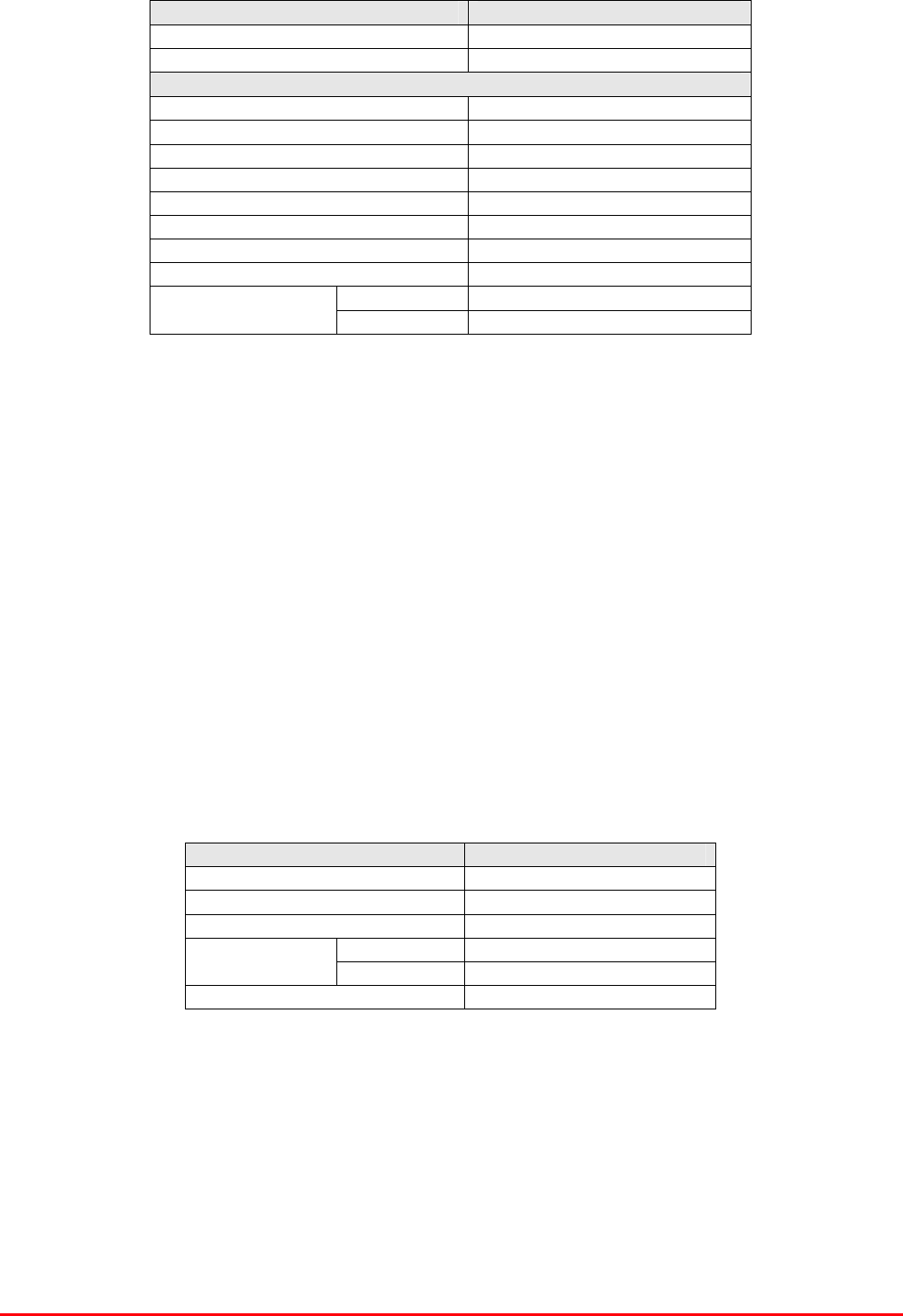
STTRS DOCUMENTATION
Document Number 80-330501HBKM – Issue A - Draft Page 365 of 500
80-008901 Specification
PARAMETER SPECIFICATION
Operating voltage 8 to 30V (floating earth)
Alarm threshold Vcc - 1.20 volt +15%
Alarm output relay contacts
Max. switch current 1.0Amp
Max. switch volts 120Vdc/60VA
Max. switch power 24W/60VA
Min. switch load 10.0µA/10.0mV
Relay isolation 1.5kV
Mechanical life >2x10⁷ operations
Relay approval BT type 56
Connector details Screw terminals
operational -10°C to +60°C Temperature
range storage -20°C to +70°C
19.3.4.10. Dual Diode Assembly (94-100004)
The purpose of these dual diode assemblies is to allow two DC voltage sources to be combined, so
that the main DC rail within the equipment can be sourced from either a mains driven PSU, or
externally through an XLR connector or from dual mains driven PSUs. They are very heavy-duty
diodes and they prevent any reverse current from flowing back to their source or the alternative
supply rail. Combining diodes such as these will also be used if the equipment is to be powered from
external back-up batteries.
19.3.4.11. DC/DC Converter 96-200047
96-200047 is an O.E.M. high power device with a wide input range and 12.5 amp @ 12V (150Watts)
output capability used to derive a 12V fixed voltage power supply rail from a higher voltage supply, in
this case 12V. In the event of failure this unit should not be repaired, only replaced.
96-200047 Specification
PARAMETER SPECIFICATION
DC Input Voltage range 19 to 36V
DC Output voltage 12V ± 1%
Max. current load 12.5Amps
Operation -10°C to +60°C Temperature
range Storage -20°C to +85°C
Working Humidity 20 to 90% RHNC

STTRS DOCUMENTATION
Document Number 80-330501HBKM – Issue A - Draft Page 366 of 500
19.3.4.12. 12V Switch-Mode PSU (96-300052)
No routine maintenance of the PSU is required. If a fault is suspected, then the output voltage from
the power supply may be measured on its output terminals. This is typically set to 12.2V. The
adjustment potentiometer will be found close to the DC output terminals.
All the PSUs used in AFL Cell Enhancers are capable of operation from either 110 or 220V nominal
AC supplies. The line voltage is sensed automatically, so no adjustment or link setting is needed by
the operator.
96-300052 Specification
AC Input Supply 110 or 220V nominal
Voltage 85 - 265V AC (absolute limits)
Frequency 47 to 63Hz
DC Output Supply 12V DC (nominal)
Voltage 10.5-13.8V (absolute limits)
Current 12.5A

STTRS DOCUMENTATION
Document Number 80-330501HBKM – Issue A - Draft Page 367 of 500
20 CONVENTION PLACE STATION 700MHZ BDA (80-330554-1)
Rack number CR1-CR-06
Convention Place Station 700MHz BDA (80-330554-1) List of major Components
Section Component
Part Component Part Description Qty Per
Assembly
20.3.1. 50-132103 700MHz Output Duplexer/Combiner 1
20.3.2. 50-132105 700MHz 5 Cavity Combiner System 1
20.3.3. 50-132106 700MHz 4 Cavity Combiner System 1
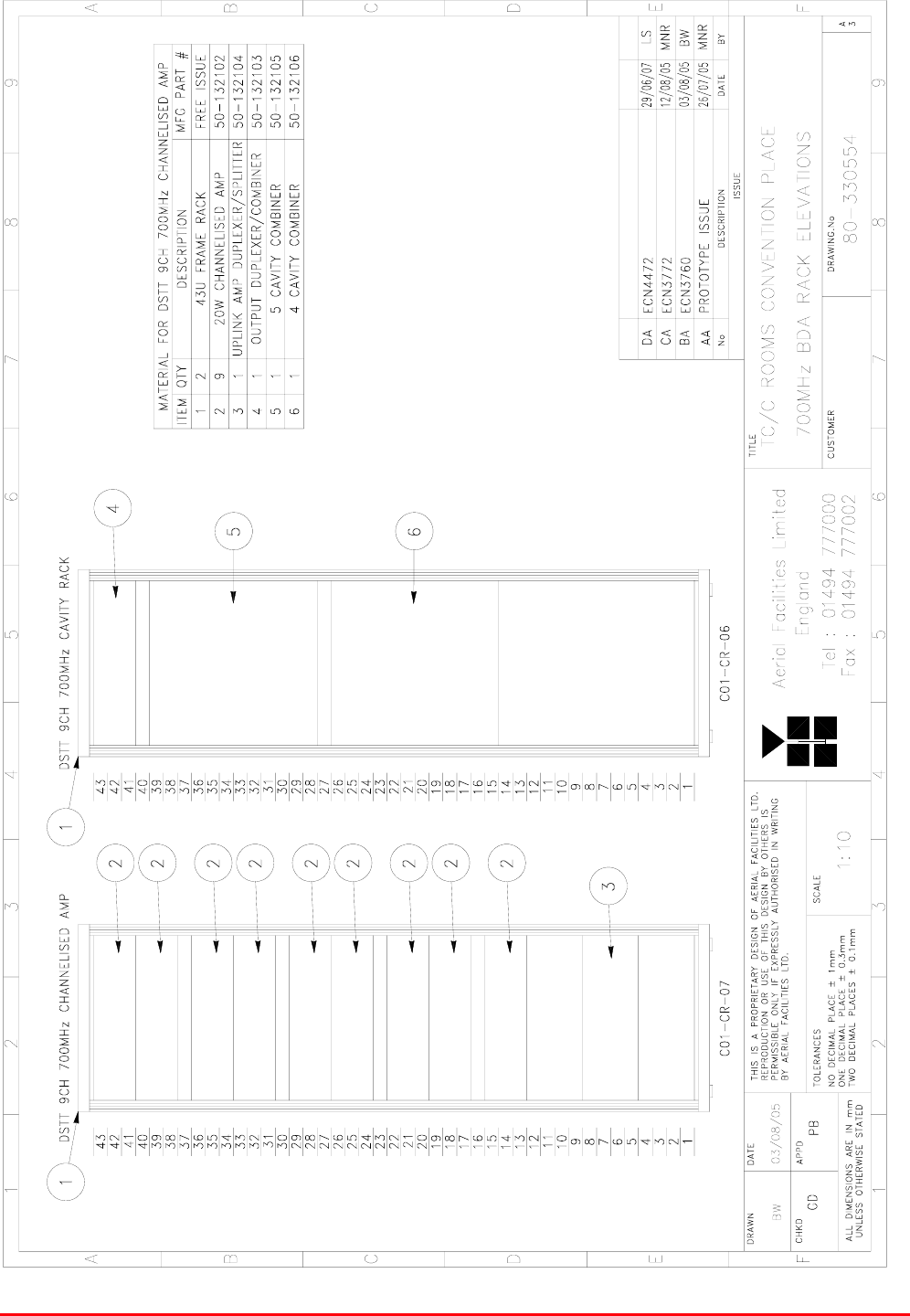
STTRS DOCUMENTATION
Document Number 80-330501HBKM – Issue A - Draft Page 368 of 500
20.1 Convention Place Station 700MHz BDA (80-330554-1) Outline Drawing
Drawing number 80-330554
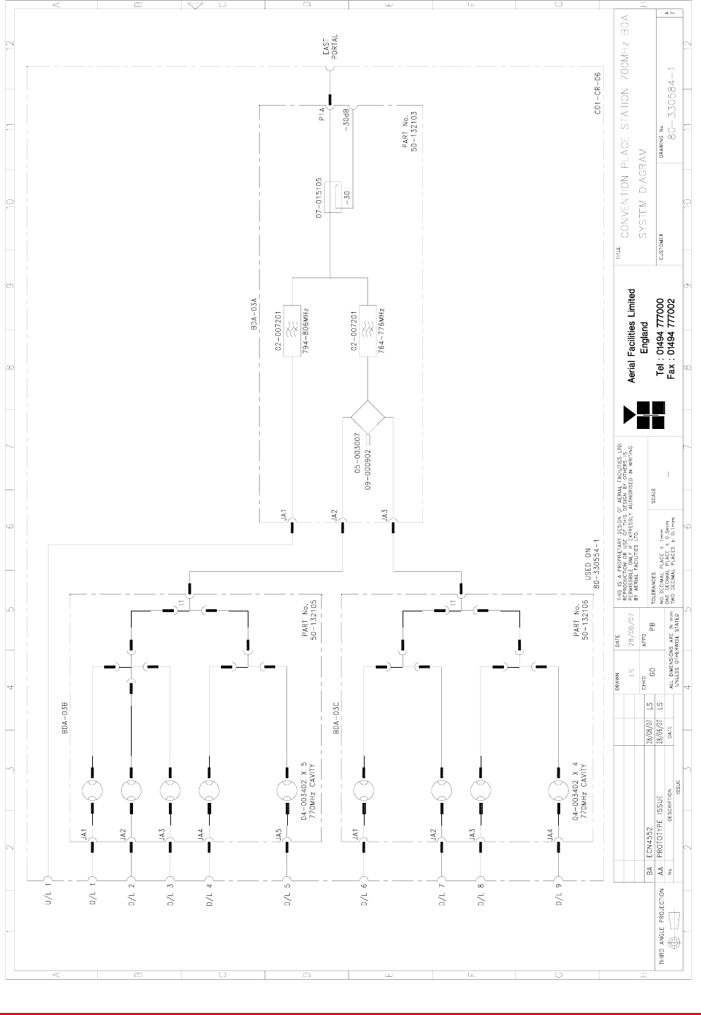
STTRS DOCUMENTATION
Document Number 80-330501HBKM – Issue A - Draft Page 369 of 500
20.2. Convention Place Station 700MHz BDA (80-330554-1) System Diagram
Drawing number 80-330584-1

STTRS DOCUMENTATION
Document Number 80-330501HBKM – Issue A - Draft Page 370 of 500
20.3 Convention Place Station 700MHz BDA (80-330554-1) Major Components
20.3.1. 700MHz Output Duplexer/Combiner (50-132103)
3U rack mount tray
700MHz Output Duplexer/Combiner (50-132103) List of Major Components
Section Component
Part Component Part Description Qty Per
Assembly
20.3.1.3. 02-007206 Bandpass Filter 2
20.3.1.4. 05-003007 4 Port Hybrid Coupler 1
20.3.1.5. 07-015105 Wideband Asymmetric Coupler 1
20.3.1.6. 09-000902 Dummy Load 1
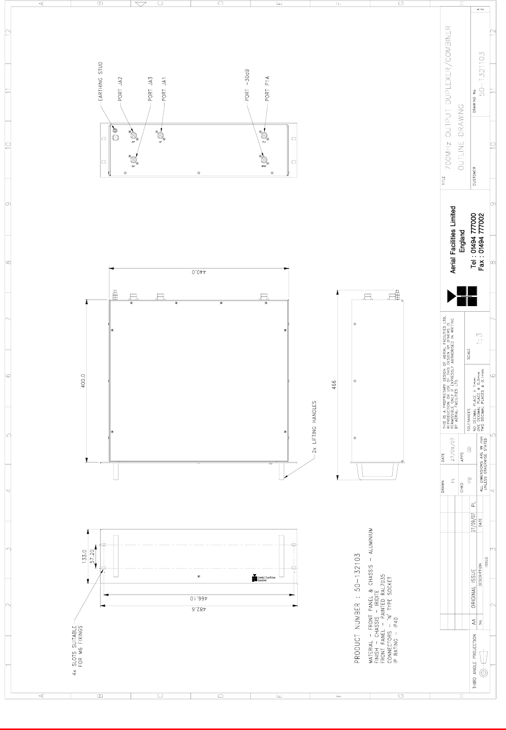
STTRS DOCUMENTATION
Document Number 80-330501HBKM – Issue A - Draft Page 371 of 500
20.3.1.1. 700MHz Output Duplexer/Combiner (50-132103) outline drawing
Drawing number 50-1321103
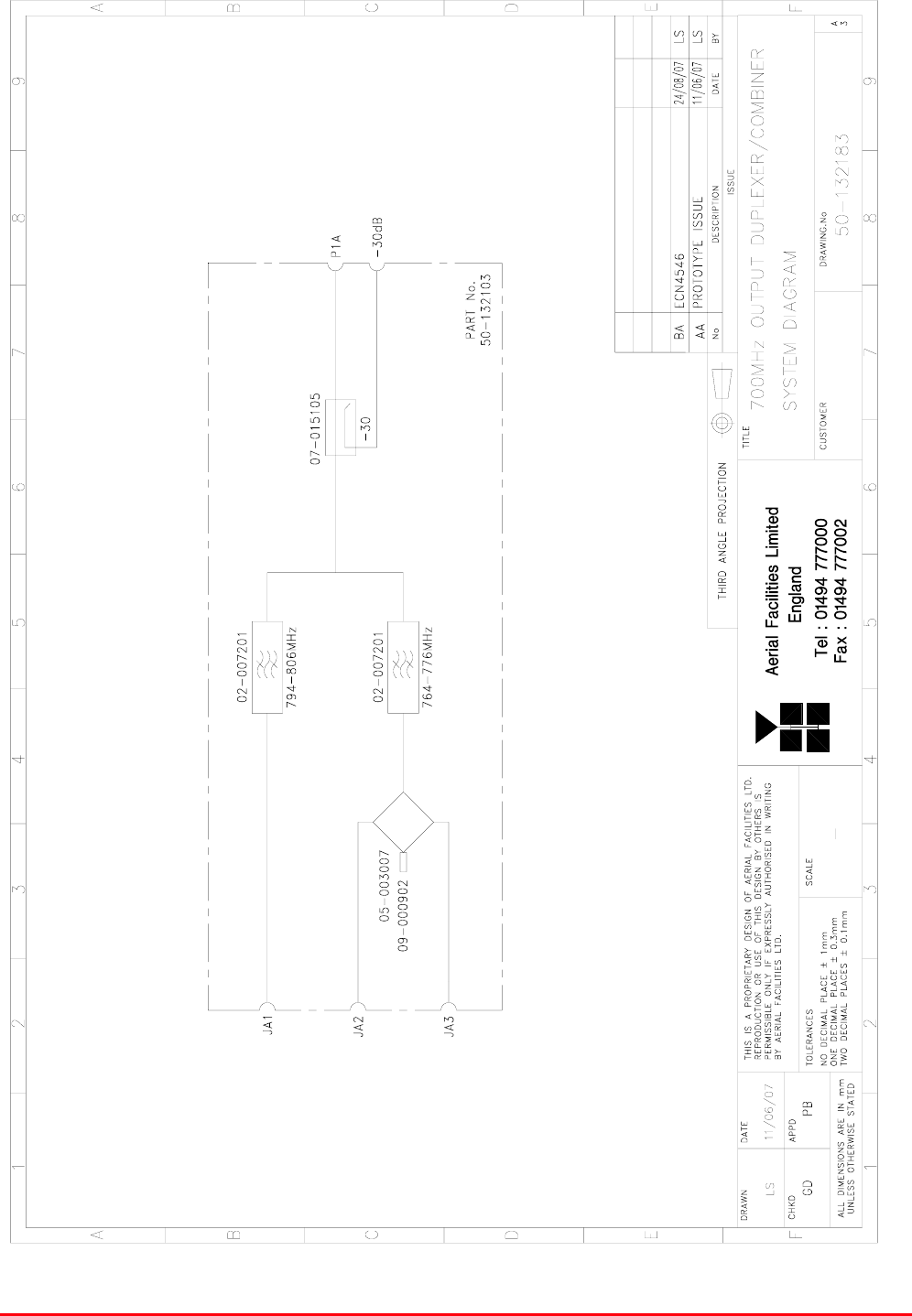
STTRS DOCUMENTATION
Document Number 80-330501HBKM – Issue A - Draft Page 372 of 500
20.3.1.2. 700MHz Output Duplexer/Combiner (50-132103) system diagram
Drawing number 50-132183
STTRS DOCUMENTATION
Document Number 80-330501HBKM – Issue A - Draft Page 373 of 500
20.3.1.3. Bandpass Filter (02-007206)
The bandpass filters are multi-section designs with a bandwidth dependent upon the passband
frequencies, (both tuned to customer requirements). The response shape is basically Chebyshev with
a passband design ripple of 0.1dB. The filters are of slot coupled, folded combline design, and are
carefully aligned during manufacture in order to optimise the insertion loss, VSWR and
intermodulation characteristics of the unit. The tuned elements are silver-plated to reduce surface
ohmic losses and maintain a good VSWR figure and 50Ω load at the input and output ports.
Being passive devices, the bandpass filters should have an extremely long operational life and require
no maintenance. Should a filter be suspect, it is usually most time efficient to replace the module
rather than attempt repair or re-tuning.
No adjustments should be attempted without full network sweep analysis facilities to monitor both
insertion loss and VSWR simultaneously.
02-007206 Specification
PARAMETER SPECIFICATION
Response type Chebyshev
Frequency range 800 - 950MHz *
Bandwidth 25MHz *
Number of sections 8
Insertion loss 1.2 dB
VSWR better than 1.2:1
Connectors SMA female
Power handling 100W max
operation -20°C to +60°C Temperature
range storage -40°C to +70°C
Weight 3 kg (typical) *tuned to Customer's specification
20.3.1.4. 4 Port Hybrid Coupler (05-003007)
This transmitter hybrid coupler is a device for accurately matching two or more RF signals to single or
multiple ports, whilst maintaining an accurate 50Ω load to all inputs/outputs and ensuring that the
insertion losses are kept to a minimum. Any unused ports should be terminated with an appropriate
50Ω load. In this specific instance one port of 4 Port Hybrid Coupler (05-003007) is terminated with
Dummy Load 09-000902 (see below).
05-003007 Specification
PARAMETER SPECIFICATION
Frequency range 700-900MHz
Bandwidth 200MHz
Rejection >14dB
Insertion loss 6.5dB (in band, typical)
Connectors SMA
Weight <1.0kg
operational -10%C to +60%C Temperature
range storage -20%C to +70%C
STTRS DOCUMENTATION
Document Number 80-330501HBKM – Issue A - Draft Page 374 of 500
20.3.1.5. Wideband Asymmetric Coupler (07-015105)
The purpose of Wideband Asymmetric Coupler (07-015105) is to tap off a known portion (in this case
30dB) of RF signal from transmission lines and to combine them, for example through splitter units for
different purposes (alarms/monitoring etc.), whilst maintaining an accurate 50Ω load to all
ports/interfaces throughout the specified frequency range. They are known formally as directional
couplers as they couple power from the RF mainline in one direction only.
07-015105 Specification
PARAMETER SPECIFICATION
Construction Inductive air gap
Frequency 800-2500MHz
Through loss 0.4dB (typical)
Coupling level -30dB ±0.5dB
Isolation N/A
Weight <1.0kg
Connectors SMA, female
operation -20°C to +60°C
Temperature
range storage -40°C to +70°C
20.3.1.6. Dummy Load 09-000902
When a combiner system is used to split or combine RF signals, in many cases it is most cost
effective to use a standard stock item 4, 6 or 8 port device where, in fact, only a 3 or 6 port device is
needed. In this case 4 Port Hybrid Coupler (05-003007) has one of its ports terminated with an
appropriate Dummy Load in order to preserve the correct impedance of the device over the specified
frequency range.
09-000902 specification
PARAMETER SPECIFICATION
Frequency Range 0 - 2500 MHz
Power Rating 25 Watts continuous
VSWR Better than 1.1:1
Impedance 50 Ohms
Temperature Range -20 to +60°C
RF Connectors N Type female
Dimension 110.3mm x 38.1mm x
Weight 485 grams
Finish Black Anodised
RF Connector N Type male
Environmental IP66
MTBF >180,000 hours

STTRS DOCUMENTATION
Document Number 80-330501HBKM – Issue A - Draft Page 375 of 500
20.3.2. 700MHz 5 Cavity Combiner System (50-132105)
700MHz 5 Cavity Combiner System (50-132105) consists of 5 Dielectric Cavity Resonators mounted
on two 3U rack mount panels, three on one panel and two on the other
700MHz 5 Cavity Combiner System (50-132105) List of Major Components
section Component
Part Component Part Description Qty Per
Assembly
20.3.2.3. 04-003402 Dielectric Cavity Resonator 5