Axell Wireless 55-165703 55-165703 Cell Enhancer User Manual 80 330501HBKM
Axell Wireless 55-165703 Cell Enhancer 80 330501HBKM
Contents
- 1. Manual 1 of 5
- 2. manual 2 of 5
- 3. manual 3 of 5
- 4. manual 4 of 5
- 5. manual 5 of 5
Manual 1 of 5

STTRS DOCUMENTATION
Document Number 80-330501HBKM – Issue A - Draft Page 1 of 500
STTRS DOCUMENTATION
User/Maintenance Handbook
For
GETS Global Signalling L.L.C.
AFL Works Order Q115525

STTRS DOCUMENTATION
Document Number 80-330501HBKM – Issue A - Draft Page 2 of 500
Table of Contents
1. INTRODUCTION ......................................................................................................................2
1.1. Scope and Purpose of Document.............................................................................................2
1.2. Limitation of Liability Notice ......................................................................................................2
2. SAFETY CONSIDERATIONS...................................................................................................2
2.1. Earthing of Equipment ..............................................................................................................2
2.2. Electric Shock Hazard...............................................................................................................2
2.3. RF Radiation Hazard ................................................................................................................2
2.4. Lifting and other Health and Safety Recommendations............................................................ 2
2.5. Chemical Hazard ......................................................................................................................2
2.6. Laser Safety..............................................................................................................................2
2.7. Emergency Contact Numbers...................................................................................................2
3. SYSTEM OVERVIEW ***///*** ..................................................................................................2
4. 800MHZ KCRS MASTER SITE (80-330651)............................................................................2
4.1. 800MHz KCRS MASTER SITE (80-330651) Drawings ............................................................ 2
4.1.1. 800MHz KCRS MASTER SITE (80-330651) Rack Elevation............................................. 2
4.1.2. 800MHz KCRS MASTER SITE (80-330651) System Diagram.......................................... 2
4.1.3. 800MHz KCRS MASTER SITE (80-330651) Alarm Wiring Diagram ................................. 2
4.2. 800MHz KCRS Master Site (80-330651) Sub Components.....................................................2
4.2.1. 800MHz FO Master Splitter/Attenuator (55-165503)..........................................................2
4.2.1.1. Four Way Splitter/Combiner (05-003302) .......................................................................2
4.2.1.2. Switched Attenuator 0.25Watt, 0 - 30dB (10-000701) .................................................... 2
4.2.1.3. Dummy Load (80-007401) ..............................................................................................2
4.2.2. F/O Link Subsystem (98-800001) ......................................................................................2
4.2.3. Optical A/B Switch FC/APC (98-700002) ........................................................................... 2
4.2.4. Fibre Optic Splitter (55-165507)......................................................................................... 2
4.2.4.1. Single Mode Optical Splitter/Coupler (98-100001).......................................................... 2
5. 700MHZ KCM MASTER SITE / PIONEER SQ (80-330652) .................................................... 2
5.1. 700MHz KCM MASTER SITE / PIONEER SQ (80-330652) Rack Elevation............................2
5.2. 700MHz KCM MASTER SITE / PIONEER SQ (80-330682) System Diagram ......................... 2
5.3. 700MHz KCM MASTER SITE / PIONEER SQ (80-330682) Alarm Wiring Diagram ***//***
Approval In progresss G.D..................................................................................................................2
5.4. 700MHz KCM MASTER SITE / PIONEER SQ (80-330682) Sub Components........................ 2
5.4.1. 800MHz Line Amplifier (55-165703)...................................................................................2
5.4.1.1. 800MHz Line Amplifier (55-165703) Outline Drawing.....................................................2
5.4.1.2. 800MHz Line Amplifier (55-165703) System Diagram.................................................... 2
5.4.1.3. Bandpass Filter (02-007206)...........................................................................................2
5.4.1.4. Wideband Asymmetric Coupler (07-015105).................................................................. 2
5.4.1.5. Switched Attenuator 0.25W, 0 - 15dB (10-000901) ........................................................ 2
5.4.1.6. Low Noise Amplifier (11-006702).................................................................................... 2
5.4.1.7. Power Amplifier (12-018002) .......................................................................................... 2
5.4.1.8. Low Power Amplifier (12-021901)...................................................................................2
5.4.1.9. Automatic Gain Control...................................................................................................2
5.4.1.10. 12V (Dual) Relay Board (20-001601) ..........................................................................2
5.4.1.11. 12V (Single) Relay Board (80-008901)........................................................................ 2
5.4.1.12. Dual Diode Assembly (94-100004)..............................................................................2
5.4.1.13. DC/DC Converter 96-200047....................................................................................... 2
5.4.1.14. 12V Switch-Mode PSU (96-300052)............................................................................ 2
5.4.2 700MHz Line Amplifier (55-165704)...................................................................................2
5.4.2.1. 700MHz Line Amplifier (55-165704) Outline Drawing.....................................................2
5.4.2.2. 700MHz Line Amplifier (55-165704) System Diagram.................................................... 2
5.4.2.3. Bandpass Filter (02-007206)...........................................................................................2

STTRS DOCUMENTATION
Document Number 80-330501HBKM – Issue A - Draft Page 3 of 500
5.4.2.4. Wideband Asymmetric Coupler (07-015105).................................................................. 2
5.4.2.5. Switched Attenuator 0.25W, 0 - 15dB (10-000901) ........................................................ 2
5.4.2.6. Low Noise Amplifier (11-006702).................................................................................... 2
5.4.2.7. Power Amplifier (12-018002) .......................................................................................... 2
5.4.2.8. Low Power Amplifier (12-021901)...................................................................................2
5.4.2.9. Automatic Gain Control...................................................................................................2
5.4.2.10. 12V (Single) Relay Board (80-008901)........................................................................ 2
5.4.2.11. Dual Diode Assembly (94-100004)..............................................................................2
5.4.2.12. DC/DC Converter 96-200047....................................................................................... 2
5.4.2.13. 12V Switch-Mode PSU (96-300052)............................................................................ 2
5.4.3. 700MHz FO MASTER ATTENUATOR (55-165604) ..........................................................2
5.4.3.1. Switched Attenuator 0.25Watt, 0 - 30dB (10-000701) .................................................... 2
5.4.4. F/O Link Subsystem (98-800001) ......................................................................................2
5.4.5. Optical AB Switch FC/APC (98-700002) ............................................................................ 2
5.4.6. Fibre Optic Splitter (55-165507)......................................................................................... 2
5.4.6.1. Single Mode Optical Splitter/Coupler (98-100001).......................................................... 2
5.4.7. PIONEER ST. SPLITTER (55-165708)..............................................................................2
5.4.7.1. 2 Way Power Splitter/ Combiner 70/30 (05-009905) ...................................................... 2
5.4.7.2. Wideband Asymmetric Coupler (07-015102).................................................................. 2
6. BEACON HILL STATION MASTER SITE 1 (80-330551-1)......................................................2
6.1. Beacon Hill Station Master Site 1 (80-330551-1) Rack Elevation............................................. 2
6.2. Beacon Hill Station Master Site 1 (80-330551-1) System Diagram.......................................... 2
Beacon Hill Station Master Site 1 (80-330551-1) Alarm Wiring Diagram ***///*** Approval In
Progress G.D. .....................................................................................................................................2
6.3. Beacon Hill Station Master Site 1 (80-330551-1) Sub Components.........................................2
6.3.1. 800MHz FO HUB AMP (55-165501) .................................................................................. 2
6.3.1.1. 800MHz FO HUB AMP (55-165501) Outline drawing..................................................... 2
6.3.1.2. 800MHz FO HUB AMP (55-165501) System Diagram ...................................................2
6.3.1.3. Bandpass Filter (02-007206)...........................................................................................2
6.3.1.4. Wideband Asymmetric Coupler (07-015105).................................................................. 2
6.3.1.5. Switched Attenuator 0.25Watt, 0 - 30dB (10-000701) .................................................... 2
6.3.1.6. Low Noise Amplifier (11-005902).................................................................................... 2
6.3.1.7. Low Noise Amplifier (11-006702).................................................................................... 2
6.3.1.8. Power Amplifier (12-018002) .......................................................................................... 2
6.3.1.9. Low Power Amplifier (12-021901)...................................................................................2
6.3.1.10. Automatic Gain Control................................................................................................ 2
6.3.1.11. 12V (Dual) Relay Board (20-001601) ..........................................................................2
6.3.1.12. 12V (Single) Relay Board (80-008901)........................................................................ 2
6.3.1.13. Dual Diode Assembly (94-100004)..............................................................................2
6.3.1.14. DC/DC Converter 96-200047....................................................................................... 2
6.3.1.15. 12V Switch-Mode PSU (96-300052)............................................................................ 2
6.3.2. 800MHz FO HUB SPLITTER/COMB (55-165502)............................................................. 2
6.3.2.1. 800MHz FO HUB SPLITTER/COMB (55-165502) Outline Drawing ............................... 2
6.3.2.2. 800MHz FO HUB SPLITTER/COMB (55-165502) System Diagram ..............................2
6.3.2.3. 900MHz Splitter/Combiner (05-002602) ......................................................................... 2
6.3.2.4. Four Way Splitter/Combiner (05-003302) .......................................................................2
6.3.3. BEACON HILL SPLITTER (BDA 1 & 3) (55-165504)......................................................... 2
6.3.3.1. BEACON HILL SPLITTER (BDA 1 & 3) (55-165504) Outline Drawing...........................2
6.3.3.2. BEACON HILL SPLITTER (BDA 1 & 3) (55-165504) System Diagram..........................2
6.3.3.3. Four Way Splitter/Combiner (05-003302) .......................................................................2
6.3.3.4. 2 Way Power Splitter/ Combiner 80/20 (05-009903) ...................................................... 2
6.3.3.5. 2 Way Power Splitter/ Combiner 70/30 (05-009905) ...................................................... 2
6.3.3.6. Wideband Asymmetric Coupler (07-015102).................................................................. 2
6.3.4. Fibre Optic Splitter (55-165507)......................................................................................... 2
6.4.3.1. Single Mode Optical Splitter/Coupler (98-100001).......................................................... 2
6.3.5. Optical AB Switch FC/APC (98-700002) ............................................................................ 2

STTRS DOCUMENTATION
Document Number 80-330501HBKM – Issue A - Draft Page 4 of 500
6.3.6. F/O Link Subsystem (98-800001) ......................................................................................2
7. BEACON HILL STATION MASTER SITE 2 (80-330551-2)......................................................2
7.1. Beacon Hill Station Master Site 2 (80-330551-2) Rack Elevation............................................. 2
7.2. Beacon Hill Station Master Site 2 (80-330551-2) System Diagram.......................................... 2
7.3. Beacon Hill Station Master Site 2 (80-330551-2) Alarm Wiring Diagram .................................2
7.4. Beacon Hill Station Master Site 2 (80-330551-2) Major Sub Components............................... 2
7.4.1. 800MHz FO HUB AMP (55-165501) .................................................................................. 2
7.4.1.1. 800MHz FO HUB AMP (55-165501) Outline drawing..................................................... 2
7.4.1.2. 800MHz FO HUB AMP (55-165501) System Diagram ...................................................2
7.4.1.3. Bandpass Filter (02-007206)...........................................................................................2
7.4.1.4. Wideband Asymmetric Coupler (07-015105).................................................................. 2
7.4.1.5. Switched Attenuator 0.25Watt, 0 - 30dB (10-000701) .................................................... 2
7.4.1.6. Low Noise Amplifier (11-005902).................................................................................... 2
7.4.1.7. Low Noise Amplifier (11-006702).................................................................................... 2
7.4.1.8. Power Amplifier (12-018002) .......................................................................................... 2
7.4.1.9. Low Power Amplifier (12-021901)...................................................................................2
7.4.1.10. Automatic Gain Control................................................................................................ 2
7.4.1.11. 12V (Dual) Relay Board (20-001601) ..........................................................................2
7.4.1.12. 12V (Single) Relay Board (80-008901)........................................................................ 2
7.4.1.13. DC/DC Converter 96-200047....................................................................................... 2
7.4.1.14. Dual Diode Assembly (94-100004)..............................................................................2
7.4.1.15. DC/DC Converter 96-200047....................................................................................... 2
7.4.1.16. 12V Switch-Mode PSU (96-300052)............................................................................ 2
7.4.2. BEACON HILL SPLITTER (BDA 2 & 4) (55-165505)......................................................... 2
7.4.2.1. BEACON HILL SPLITTER (BDA 2 & 4) (55-165505) Outline Drawing...........................2
7.4.2.2. BEACON HILL SPLITTER (BDA 2 & 4) (55-165505) System Diagram..........................2
7.4.2.3. 2 Way Power Splitter/ Combiner 70/30 (05-009905) ...................................................... 2
7.4.2.4. 3 Way Power Splitter 33/33/33 (05-009906) ***///*** BSB ..............................................2
7.4.2.5. 3 Way Power Splitter 40/20/40 (05-009907) ***///***BSB ...............................................2
7.4.2.6. Wideband Asymmetric Coupler (07-015102).................................................................. 2
8 BEACON HILL STATION CROSS PASSAGE A (80-330591-1) .....................................................2
8.1. Beacon Hill Station Cross Passage A (80-330591-1) Rack Layout ***///***..............................2
8.2. Beacon Hill Station Cross Passage A (80-330591-1) System Diagram ...................................2
8.3. Beacon Hill Station Cross Passage A (80-330591-1) Alarm Wiring Diagram...........................2
8.4. Beacon Hill Station Cross Passage A (80-330591-1) Major Sub Components ........................ 2
8.4.1. Wideband Asymmetric Coupler (07-015102) ..................................................................... 2
8.4.2. Power Amplifier (12-018002)..............................................................................................2
8.4.3. 800MHz Line Amplifier (Ext. Amp.) (55-165401)................................................................ 2
8.4.3.1. 800MHz Line Amplifier (Ext. Amp.) (55-165401) outline drawing ................................... 2
8.4.3.2. 800MHz Line Amplifier (Ext. Amp.) (55-165401) system diagram..................................2
8.4.3.3. Bandpass Filter (02-007206)...........................................................................................2
8.4.3.4. Wideband Asymmetric Coupler (07-015105).................................................................. 2
8.4.3.5. Switched Attenuator 0.25W, 0 - 15dB (10-000901) ........................................................ 2
8.4.3.6. Low Noise Amplifier (11-006702).................................................................................... 2
8.4.3.7. Power Amplifier (12-018002) .......................................................................................... 2
8.4.3.8. Low Power Amplifier (12-021901)...................................................................................2
8.4.3.9. Automatic Gain Control...................................................................................................2
8.4.3.10. 12V (Single) Relay Board (80-008901)........................................................................ 2
8.4.3.11. Dual Diode Assembly (94-100004)..............................................................................2
8.4.3.12. DC/DC Converter (96-200047) ....................................................................................2
8.4.3.13. 12V Switch-Mode PSU (96-300052)............................................................................ 2
9 BEACON HILL STATION CROSS PASSAGE B (80-330591-2) .....................................................2
9.1. Beacon Hill Station Cross Passage B (80-330591-2) Rack layout ***///***...............................2
9.2. Beacon Hill Station Cross Passage B (80-330591-2) System Diagram ...................................2
9.3. Beacon Hill Station Cross Passage B (80-330591-2) Alarm Wiring Diagram...........................2
9.4. Beacon Hill Station Cross Passage A (80-330591-1) Major Sub Components ........................ 2
9.4.1. Wideband Asymmetric Coupler (07-015102) ..................................................................... 2

STTRS DOCUMENTATION
Document Number 80-330501HBKM – Issue A - Draft Page 5 of 500
9.4.2. Power Amplifier (12-018002)..............................................................................................2
9.4.3. 800MHz Line Amplifier (Ext. Amp.) (55-165401)................................................................ 2
9.4.3.1. 800MHz Line Amplifier (Ext. Amp.) (55-165401) outline drawing ................................... 2
9.4.3.2. 800MHz Line Amplifier (Ext. Amp.) (55-165401) system diagram..................................2
9.4.3.3. Bandpass Filter (02-007206)...........................................................................................2
9.4.3.4. Wideband Asymmetric Coupler (07-015105).................................................................. 2
9.4.3.5. Switched Attenuator 0.25W, 0 - 15dB (10-000901) ........................................................ 2
9.4.3.6. Low Noise Amplifier (11-006702).................................................................................... 2
9.4.3.7. Power Amplifier (12-018002) .......................................................................................... 2
9.4.3.8. Low Power Amplifier (12-021901)...................................................................................2
9.4.3.9. Automatic Gain Control...................................................................................................2
9.4.3.10. 12V (Single) Relay Board (80-008901)........................................................................ 2
9.4.3.11. Dual Diode Assembly (94-100004)..............................................................................2
9.4.3.12. DC/DC Converter 96-200047....................................................................................... 2
9.4.3.12. 12V Switch-Mode PSU (96-300052)............................................................................ 2
10. UNIVERSITY STATION MASTER SITE 1 (80-330552-1) ........................................................ 2
10.1. University Station Master Site 1 (80-330552-1) Rack elevation ............................................2
10.2. University Station Master Site 1 (80-330552-1) system diagram .......................................... 2
10.3. University Station Master Site 1 (80-330552-1) Alarm Wiring Diagram................................. 2
10.4 University Station Master Site 1 (80-330552-1) Major Components ..................................... 2
10.4.1. 800MHz FO HUB Splitter/Combiner (55-165502)........................................................... 2
10.4.1.1. 800MHz FO HUB SPLITTER/COMB (55-165502) Outline Drawing............................ 2
10.4.1.2. 800MHz FO HUB SPLITTER/COMB (55-165502) System Diagram...........................2
10.4.1.3. 900MHz Splitter/Combiner (05-002602) ...................................................................... 2
10.4.1.4. Four Way Splitter/Combiner (05-003302)....................................................................2
10.4.2. Fibre Optic Splitter (55-165507)...................................................................................... 2
10.4.2.1. Single Mode Optical Splitter/Coupler (98-100001) ......................................................2
10.4.3. 800MHz FO Hub Amplifier + Filters (55-165601)............................................................ 2
10.4.3.1. 800MHz FO Hub Amplifier + Filters (55-165601) outline drawing ............................... 2
10.4.3.2. 800MHz FO Hub Amplifier + Filters (55-165601) system diagram .............................. 2
10.4.3.3. Bandpass Filter (02-007206) ....................................................................................... 2
10.4.3.4. Wideband Asymmetric Coupler (07-015105)............................................................... 2
10.4.3.5. Switched Attenuator 0.25Watt, 0 - 30dB (10-000701) ................................................. 2
10.4.3.6. Low Noise Amplifier (11-005902) ................................................................................2
10.4.3.7. Low Noise Amplifier (11-006702) ................................................................................2
10.4.3.8. Power Amplifier (12-018002) ....................................................................................... 2
10.4.3.9. Low Power Amplifier (12-021901)................................................................................2
10.4.3.10. Automatic Gain Control ............................................................................................... 2
10.4.3.11. 12V (Dual) Relay Board (20-001601).......................................................................... 2
10.4.3.12. 12V (Single) Relay Board (80-008901) ....................................................................... 2
10.4.3.13. Dual Diode Assembly (94-100004).............................................................................. 2
10.4.3.14. DC/DC Converter 96-200047 ...................................................................................... 2
10.4.3.15. 12V Switch-Mode PSU (96-300052) ........................................................................... 2
10.4.4. 700MHz FO Hub Amplifier (55-165602).......................................................................... 2
10.4.4.1. 700MHz FO Hub Amplifier (55-165602) Outline Drawing............................................2
10.4.4.2. 700MHz FO Hub Amplifier (55-165602) system diagram............................................ 2
10.4.4.3. Bandpass Filter (02-007206) ....................................................................................... 2
10.4.4.4. Wideband Asymmetric Coupler (07-015105)............................................................... 2
10.4.4.5. Switched Attenuator 0.25Watt, 0 - 30dB (10-000701) ................................................. 2
10.4.4.6. Low Noise Amplifier (11-005902) ................................................................................2
10.4.4.7. Low Noise Amplifier (11-006702) ................................................................................2
10.4.4.8. Power Amplifier (12-018002) ....................................................................................... 2
10.4.4.9. Low Power Amplifier (12-021901)................................................................................2
10.4.4.10. Automatic Gain Control ............................................................................................... 2
10.4.4.11. 12V (Dual) Relay Board (20-001601).......................................................................... 2
10.4.4.12. 12V (Single) Relay Board (80-008901) ....................................................................... 2
10.4.4.13. Dual Diode Assembly (94-100004).............................................................................. 2
10.4.4.14. DC/DC Converter 96-200047 ...................................................................................... 2

STTRS DOCUMENTATION
Document Number 80-330501HBKM – Issue A - Draft Page 6 of 500
10.4.4.15. 12V Switch-Mode PSU (96-300052) ........................................................................... 2
10.4.5. University Station Splitter 1 (55-165711) ........................................................................ 2
10.4.5.1. University Station Splitter 1 (55-165711) outline drawing............................................2
10.4.5.2. University Station Splitter 1 (55-165711) system diagram........................................... 2
10.4.5.3. 2-Way Splitter/Combiner (05-003005) ......................................................................... 2
10.4.5.4. Wideband Asymmetric Coupler (07-015102)............................................................... 2
10.4.6. Optical AB Switch FC/APC (98-700002).........................................................................2
10.4.7. F/O Link Subsystem (98-800001) ...................................................................................2
11. UNIVERSITY STATION MASTER SITE 2 (80-330552-2) ........................................................ 2
11.1. University Station Master Site 2 (80-330552-1) Rack elevation ............................................2
11.2. University Station Master Site 2 (80-330552-1) system diagram .......................................... 2
11.3. University Station Master Site 2 (80-330552-1) Alarm Wiring Diagram................................. 2
11.4 University Station Master Site 2 (80-330552-1) Major Components ..................................... 2
11.4.1. Fibre Optic Splitter (55-165507)...................................................................................... 2
11.4.1.1. Single Mode Optical Splitter/Coupler (98-100001) ......................................................2
11.4.2. 800MHz FO Hub Amplifier + Filters (55-165601)............................................................ 2
11.4.2.1. 800MHz FO Hub Amplifier + Filters (55-165601) outline drawing ............................... 2
11.4.2.2. 800MHz FO Hub Amplifier + Filters (55-165601) system diagram .............................. 2
11.4.2.3. Bandpass Filter (02-007206) ....................................................................................... 2
11.4.2.4. Wideband Asymmetric Coupler (07-015105)............................................................... 2
11.4.2.5. Switched Attenuator 0.25Watt, 0 - 30dB (10-000701) ................................................. 2
11.4.2.6. Low Noise Amplifier (11-005902) ................................................................................2
11.4.2.7. Low Noise Amplifier (11-006702) ................................................................................2
11.4.2.8. Power Amplifier (12-018002) ....................................................................................... 2
11.4.2.9. Low Power Amplifier (12-021901)................................................................................2
11.4.2.10. Automatic Gain Control ............................................................................................... 2
11.4.2.11. 12V (Dual) Relay Board (20-001601).......................................................................... 2
11.4.2.12. 12V (Single) Relay Board (80-008901) ....................................................................... 2
11.4.2.13. Dual Diode Assembly (94-100004).............................................................................. 2
11.4.2.14. DC/DC Converter 96-200047 ...................................................................................... 2
11.4.2.15. 12V Switch-Mode PSU (96-300052) ........................................................................... 2
11.4.3. 700MHz FO Hub Amplifier (55-165602).......................................................................... 2
11.4.3.1. 700MHz FO Hub Amplifier (55-165602) outline drawing .............................................2
11.4.3.2. 700MHz FO Hub Amplifier (55-165602) system diagram............................................ 2
11.4.3.3. Bandpass Filter (02-007206) ....................................................................................... 2
11.4.3.4. Wideband Asymmetric Coupler (07-015105)............................................................... 2
11.4.3.5. Switched Attenuator 0.25Watt, 0 - 30dB (10-000701) ................................................. 2
11.4.3.6. Low Noise Amplifier (11-005902) ................................................................................2
11.4.3.7. Low Noise Amplifier (11-006702) ................................................................................2
11.4.3.8. Power Amplifier (12-018002) ....................................................................................... 2
111.4.3.9. Low Power Amplifier (12-021901) ...............................................................................2
11.4.3.10. Automatic Gain Control ............................................................................................... 2
11.4.3.11. 12V (Dual) Relay Board (20-001601).......................................................................... 2
11.4.3.12. 12V (Single) Relay Board (80-008901) ....................................................................... 2
11.4.3.13. Dual Diode Assembly (94-100004).............................................................................. 2
11.4.3.14. DC/DC Converter 96-200047 ...................................................................................... 2
11.4.3.15. 12V Switch-Mode PSU (96-300052) ........................................................................... 2
11.4.4. 700MHz FO HUB Splitter/Combiner (55-165603)........................................................... 2
11.4.4.2. Four Way Splitter/Combiner (05-003302)....................................................................2
11.4.5. UNIVERSITY ST. SPLITTER 2 (55-165712) .................................................................. 2
11.4.5.1. University Station Splitter 2 (55-165712) outline drawing............................................2
11.4.5.2. University Station Splitter 2 (55-165712) system diagram........................................... 2
11.4.5.3. Wideband Asymmetric Coupler (07-015102)............................................................... 2
11.4.6. Optical AB Switch FC/APC (98-700002).........................................................................2
11.4.7. F/O Link Subsystem (98-800001) ...................................................................................2
12. WESTLAKE STATION LINE AMPLIFIER (80-330553) ............................................................2

STTRS DOCUMENTATION
Document Number 80-330501HBKM – Issue A - Draft Page 7 of 500
12.1. Westlake Station Line Amplifier (80-330553) rack elevation ................................................. 2
12.2. Westlake Station Line Amplifier (80-330553) system diagram..............................................2
12.3. Westlake Station Line Amplifier (80-330553) alarm wiring diagram......................................2
12.4. Westlake Station Line Amplifier (80-330553) Sub Components............................................2
12.4.1. 800MHz Line Amplifier (55-165703) ............................................................................... 2
12.4.1.1. 800MHz Line Amplifier (55-165703) Outline Drawing.................................................. 2
12.4.1.2. 800MHz Line Amplifier (55-165703) System Diagram................................................. 2
12.4.1.3. Bandpass Filter (02-007206) ....................................................................................... 2
12.4.1.4. Wideband Asymmetric Coupler (07-015105)............................................................... 2
12.4.1.5. Switched Attenuator 0.25W, 0 - 15dB (10-000901) ..................................................... 2
12.4.1.6. Low Noise Amplifier (11-006702) ................................................................................2
12.4.1.7. Power Amplifier (12-018002) ....................................................................................... 2
12.4.1.8. Low Power Amplifier (12-021901)................................................................................2
12.4.1.9. Automatic Gain Control................................................................................................ 2
12.4.1.10. 12V (Dual) Relay Board (20-001601).......................................................................... 2
12.4.1.11. 12V (Single) Relay Board (80-008901) ....................................................................... 2
12.4.1.12. Dual Diode Assembly (94-100004).............................................................................. 2
12.4.1.13. DC/DC Converter 96-200047 ...................................................................................... 2
12.4.1.14. 12V Switch-Mode PSU (96-300052) ........................................................................... 2
12.4.2 700MHz Line Amplifier (55-165704)...................................................................................2
12.4.2.1. 700MHz Line Amplifier (55-165704) Outline Drawing.................................................. 2
12.4.2.2. 700MHz Line Amplifier (55-165704) System Diagram................................................. 2
12.4.2.3. Bandpass Filter (02-007206) ....................................................................................... 2
12.4.2.4. Wideband Asymmetric Coupler (07-015105)............................................................... 2
12.4.2.5. Switched Attenuator 0.25W, 0 - 15dB (10-000901) ..................................................... 2
12.4.2.6. Low Noise Amplifier (11-006702) ................................................................................2
12.4.2.7. Power Amplifier (12-018002) ....................................................................................... 2
12.4.2.8. Low Power Amplifier (12-021901)................................................................................2
12.4.2.9. Automatic Gain Control................................................................................................ 2
12.4.2.10. 12V (Single) Relay Board (80-008901) ....................................................................... 2
12.4.2.11. Dual Diode Assembly (94-100004).............................................................................. 2
12.4.2.12. DC/DC Converter 96-200047 ...................................................................................... 2
12.4.2.13. 12V Switch-Mode PSU (96-300052) ........................................................................... 2
12.4.3. Westlake Station. Splitter (55-165707) ...........................................................................2
12.4.3.1. Westlake Station. Splitter (55-165707) outline drawing............................................... 2
12.4.3.2. Westlake Station. Splitter (55-165707) system diagram.............................................. 2
12.4.3.3. Wideband Asymmetric Coupler (07-015102)............................................................... 2
13 ATTENUATOR SHELF (ITAC) 1 (55-165506).......................................................................... 2
13.1. Attenuator Shelf (ITAC) 1 (55-165506) outline drawing.........................................................2
13.2 Attenuator Shelf (ITAC) 1 (55-165506) system diagram ....................................................... 2
13.3. Attenuator Shelf (ITAC) 1 (55-165506) major components ...................................................2
13.3.1. 900MHz Splitter/Combiner (05-002602) ......................................................................... 2
13.3.2. 4 Port Hybrid Coupler (05-003007)................................................................................. 2
13.3.3. Dummy load (09-000902) ............................................................................................... 2
13.3.4. Switched Attenuator 0.25W, 0 - 15dB (10-000901) ........................................................ 2
13.3.5. Attenuator 25W, 60dB (10-002960) ................................................................................2
14 ATTENUATOR SHELF (ITAC) 2 (55-165506).......................................................................... 2
14.1. Attenuator Shelf (ITAC) 2 (55-165506) outline drawing.........................................................2
14.2 Attenuator Shelf (ITAC) 2 (55-165506) system diagram ....................................................... 2
14.3. Attenuator Shelf (ITAC) 2 (55-165506) major components ...................................................2
14.3.1. 900MHz Splitter/Combiner (05-002602) ......................................................................... 2
14.3.2. 4 Port Hybrid Coupler (05-003007)................................................................................. 2
14.3.3. Dummy load 09-000902..................................................................................................2
14.3.4. Switched Attenuator 0.25W, 0 - 15dB (10-000901) ........................................................ 2
14.3.5. Attenuator 25W, 60dB (10-002960) ................................................................................2
15 ATTENUATOR SHELF (ITAC) 3 (55-165506).......................................................................... 2

STTRS DOCUMENTATION
Document Number 80-330501HBKM – Issue A - Draft Page 8 of 500
15.1. Attenuator Shelf (ITAC) 3 (55-165506) outline drawing.........................................................2
15.2 Attenuator Shelf (ITAC) 3 (55-165506) system diagram ....................................................... 2
15.3. Attenuator Shelf (ITAC) 3 (55-165506) major components ...................................................2
15.3.1. 900MHz Splitter/Combiner (05-002602) ......................................................................... 2
15.3.2. 4 Port Hybrid Coupler (05-003007)................................................................................. 2
15.3.3. Dummy Load (09-000902) ..............................................................................................2
15.3.4. Switched Attenuator 0.25W, 0 - 15dB (10-000901) ........................................................ 2
15.3.5. Attenuator 25W, 60dB (10-002960) ................................................................................2
16. CONVENTION PLACE STATION LINE AMPLIFIER (80-330556) ...........................................2
16.1. Convention Place Station Line Amp. (80-330556) Rack elevation........................................2
16.2. Convention Place Station Line Amp. (80-330556) System diagram...................................... 2
16.3. Convention Place Station Line Amp. (80-330556) Alarm wiring diagram..............................2
16.4 Convention Place Station Line Amp. (80-330556) Sub Components .........................................2
16.4.1. 800MHz Line Amplifier (55-165703) ............................................................................... 2
16.4.1.1. 800MHz Line Amplifier (55-165703) Outline Drawing.................................................. 2
16.4.1.2. 800MHz Line Amplifier (55-165703) System Diagram................................................. 2
16.4.1.3. Bandpass Filter (02-007206) ....................................................................................... 2
16.4.1.4. Wideband Asymmetric Coupler (07-015105)............................................................... 2
16.4.1.5. Switched Attenuator 0.25W, 0 - 15dB (10-000901) ..................................................... 2
16.4.1.6. Low Noise Amplifier (11-006702) ................................................................................2
16.4.1.7. Power Amplifier (12-018002) ....................................................................................... 2
16.4.1.8. Low Power Amplifier (12-021901)................................................................................2
16.4.1.9. Automatic Gain Control................................................................................................ 2
16.4.1.10. 12V (Dual) Relay Board (20-001601).......................................................................... 2
16.4.1.11. 12V (Single) Relay Board (80-008901) ....................................................................... 2
16.4.1.12. Dual Diode Assembly (94-100004).............................................................................. 2
16.4.1.13. DC/DC Converter 96-200047 ...................................................................................... 2
16.4.1.14. 12V Switch-Mode PSU (96-300052) ........................................................................... 2
16.4.2 700MHz Line Amplifier (55-165704)...................................................................................2
16.4.2.1. 700MHz Line Amplifier (55-165704) Outline Drawing.................................................. 2
16.4.2.2. 700MHz Line Amplifier (55-165704) System Diagram................................................. 2
16.4.2.3. Bandpass Filter (02-007206) ....................................................................................... 2
16.4.2.4. Wideband Asymmetric Coupler (07-015105)............................................................... 2
16.4.2.5. Switched Attenuator 0.25W, 0 - 15dB (10-000901) ..................................................... 2
16.4.2.6. Low Noise Amplifier (11-006702) ................................................................................2
16.4.2.7. Power Amplifier (12-018002) ....................................................................................... 2
16.4.2.8. Low Power Amplifier (12-021901)................................................................................2
16.4.2.9. Automatic Gain Control................................................................................................ 2
16.4.2.10. 12V (Single) Relay Board (80-008901) ....................................................................... 2
16.4.2.11. Dual Diode Assembly (94-100004).............................................................................. 2
16.4.2.12. DC/DC Converter 96-200047 ...................................................................................... 2
16.3.2.13. 12V Switch-Mode PSU (96-300052) ........................................................................... 2
16.4.3. Convention Place Station Splitter (55-165709)...............................................................2
16.4.3.1. Convention Place Station Splitter (55-165709) outline drawing ..................................2
16.4.3.2. Convention Place Station Splitter (55-165709) system diagram .................................2
16.4.3.3. 900MHz Splitter/Combiner (05-002602) ...................................................................... 2
16.4.3.4. Wideband Asymmetric Coupler (07-015102)............................................................... 2
17. INTERNATIONAL (NO NPSPAC) LINE AMPLIFIER (80-330557) ...........................................2
17.1. International (no NPSPAC) Line Amp. (80-330557) Rack elevation ..................................... 2
17.2. International (no NPSPAC) Line Amp. (80-330557) System diagram................................... 2
17.3. International (no NPSPAC) Line Amp. (80-330557) Alarm wiring diagram ...........................2
17.4. International (no NPSPAC) Line Amp. (80-330557) major components ............................... 2
17.4.1. 800MHz Line Amplifier (no NPSPAC) (55-165705) ........................................................ 2
17.4.1.1. 800MHz Line Amplifier (no NPSPAC) (55-165705) Outline Drawing .......................... 2
14.4.1.2. 800MHz Line Amplifier (no NPSPAC) (55-165705) System Diagram .........................2
17.4.1.3. Bandpass Filter (02-012701) ....................................................................................... 2
17.4.1.4. Bandpass Filter (02-007206) ....................................................................................... 2

STTRS DOCUMENTATION
Document Number 80-330501HBKM – Issue A - Draft Page 9 of 500
17.4.1.5. Wideband Asymmetric Coupler (07-015105)............................................................... 2
17.4.1.6. Switched Attenuator 0.25W, 0 - 15dB (10-000901) ..................................................... 2
17.4.1.7. Low Noise Amplifier (11-006702) ................................................................................2
17.4.1.8. Power Amplifier (12-018002) ....................................................................................... 2
17.4.1.9. Low Power Amplifier (12-021901)................................................................................2
7.4.1.10. Automatic Gain Control................................................................................................ 2
17.4.1.11. 12V (Single) Relay Board (80-008901) ....................................................................... 2
17.4.1.12. Dual Diode Assembly (94-100004).............................................................................. 2
17.4.1.13. DC/DC Converter 96-200047 ...................................................................................... 2
17.4.1.14. 12V Switch-Mode PSU (96-300052) ........................................................................... 2
17.4.2. 700MHz Line Amplifier (no NPSPAC) (55-165706) ........................................................ 2
17.4.2.1. 700MHz Line Amplifier (no NPSPAC) (55-165706) Outline Drawing .......................... 2
17.4.2.2. 700MHz Line Amplifier (no NPSPAC) (55-165706) System Diagram .........................2
17.4.2.3. Bandpass Filter (02-012701) ....................................................................................... 2
17.4.2.4. Bandpass Filter (02-007206) ....................................................................................... 2
17.4.2.5. Wideband Asymmetric Coupler (07-015105)............................................................... 2
17.4.2.6. Switched Attenuator 0.25W, 0 - 15dB (10-000901) ..................................................... 2
17.4.2.7. Low Noise Amplifier (11-006702) ................................................................................2
17.4.2.8. Power Amplifier (12-018002) ....................................................................................... 2
17.4.2.9. Low Power Amplifier (12-021901)................................................................................2
7.4.2.10. Automatic Gain Control................................................................................................ 2
17.4.2.11. 12V (Single) Relay Board (80-008901) ....................................................................... 2
17.4.2.12. Dual Diode Assembly (94-100004).............................................................................. 2
17.4.2.13. DC/DC Converter 96-200047 ...................................................................................... 2
17.4.2.14. 12V Switch-Mode PSU (96-300052) ........................................................................... 2
17.4.3. International Station Splitter (55-165710) .......................................................................2
17.4.3.1. International Station Splitter (55-165710) Outline drawing .......................................... 2
17.4.3.2. International Station Splitter (55-165710) System Diagram.........................................2
17.4.3.3. 900MHz Splitter/Combiner (05-002602) ...................................................................... 2
17.4.3.4. 05-009909 – BSB to provide spec ***///***................................................................... 2
17.4.3.5. Wideband Asymmetric Coupler (07-015102)............................................................... 2
18. UNIVERSITY STATION CROSS PASSAGE A (80-330590-1)................................................2
18.1. University Station Cross Passage A (80-330590-1) System Diagram................................... 2
18.2. University Station Cross Passage A (80-330590-1) Alarm Wiring Diagram.......................... 2
18.3. University Station Cross Passage A (80-330590-1) Major Sub Components ....................... 2
18.3.1. Wideband Asymmetric Coupler (07-015102).................................................................. 2
18.3.2. Power Amplifier (12-018002) .......................................................................................... 2
18.3.3. 800MHz Line Amplifier (55-165701) ............................................................................... 2
18.3.3.1. 800MHz Line Amplifier (55-165701) Outline Drawing.................................................. 2
18.3.3.2. 800MHz Line Amplifier (55-165701) System Diagram................................................. 2
18.3.3.3. Bandpass Filter (02-007206) ....................................................................................... 2
18.3.3.4. Wideband Asymmetric Coupler (07-015105)............................................................... 2
18.3.3.5. Switched Attenuator 0.25W, 0 - 15dB (10-000901) ..................................................... 2
18.3.3.6. Low Noise Amplifier (11-006702) ................................................................................2
18.3.3.7. Low Power Amplifier (12-021901)................................................................................2
18.3.3.8. Automatic Gain Control................................................................................................ 2
18.3.3.9. 12V (Single) Relay Board (80-008901)........................................................................ 2
18.3.3.10. Dual Diode Assembly (94-100004).............................................................................. 2
18.3.3.11. DC/DC Converter 96-200047 ...................................................................................... 2
18.3.3.12. 12V Switch-Mode PSU (96-300052) ........................................................................... 2
18.3.4. 700MHz Line Amplifier (55-165702) ............................................................................... 2
18.3.4.2. 700MHz Line Amplifier (55-165702) System Diagram................................................. 2
18.3.4.3. Bandpass Filter (02-007206) ....................................................................................... 2
18.3.4.4. Wideband Asymmetric Coupler (07-015105)............................................................... 2
18.3.4.5. Switched Attenuator 0.25W, 0 - 15dB (10-000901) ..................................................... 2
18.3.4.6. Low Noise Amplifier (11-006702) ................................................................................2
18.3.4.7. Low Power Amplifier (12-021901)................................................................................2
18.3.4.8. Automatic Gain Control................................................................................................ 2

STTRS DOCUMENTATION
Document Number 80-330501HBKM – Issue A - Draft Page 10 of 500
18.3.4.9. 12V (Single) Relay Board (80-008901)........................................................................ 2
18.3.4.10. Dual Diode Assembly (94-100004).............................................................................. 2
18.3.4.11. DC/DC Converter 96-200047 ...................................................................................... 2
18.3.4.12. 12V Switch-Mode PSU (96-300052) ........................................................................... 2
19. UNIVERSITY STATION CROSS PASSAGE B (80-330590-2)................................................2
19.1. University Station Cross Passage B (80-330590-2) System Diagram................................... 2
19.2. University Station Cross Passage B (80-330590-2) Alarm Wiring Diagram.......................... 2
19.3. University Station Cross Passage B (80-330590-2) Major Sub Components ....................... 2
19.3.1. Wideband Asymmetric Coupler (07-015102).................................................................. 2
19.3.2. Power Amplifier (12-018002) .......................................................................................... 2
19.3.3. 800MHz Line Amplifier (55-165701) ............................................................................... 2
19.3.3.1. 800MHz Line Amplifier (55-165701) Outline Drawing.................................................. 2
19.3.3.2. 800MHz Line Amplifier (55-165701) System Diagram................................................. 2
19.3.3.3. Bandpass Filter (02-007206) ....................................................................................... 2
19.3.3.4. Wideband Asymmetric Coupler (07-015105)............................................................... 2
19.3.3.5. Switched Attenuator 0.25W, 0 - 15dB (10-000901) ..................................................... 2
19.3.3.6. Low Noise Amplifier (11-006702) ................................................................................2
19.3.3.7. Low Power Amplifier (12-021901)................................................................................2
19.3.3.8. Automatic Gain Control................................................................................................ 2
19.3.3.9. 12V (Single) Relay Board (80-008901)........................................................................ 2
19.3.3.10. Dual Diode Assembly (94-100004).............................................................................. 2
19.3.3.11. DC/DC Converter 96-200047 ...................................................................................... 2
19.3.3.12. 12V Switch-Mode PSU (96-300052) ........................................................................... 2
19.3.4. 700MHz Line Amplifier (55-165702) ............................................................................... 2
19.3.4.1. 700MHz Line Amplifier (55-165702) Outline Drawing.................................................. 2
19.3.4.2. 700MHz Line Amplifier (55-165702) System Diagram................................................. 2
19.3.4.3. Bandpass Filter (02-007206) ....................................................................................... 2
19.3.4.4. Wideband Asymmetric Coupler (07-015105)............................................................... 2
19.3.4.5. Switched Attenuator 0.25W, 0 - 15dB (10-000901) ..................................................... 2
19.3.4.6. Low Noise Amplifier (11-006702) ................................................................................2
19.3.4.7. Low Power Amplifier (12-021901)................................................................................2
19.3.4.8. Automatic Gain Control................................................................................................ 2
19.3.4.9. 12V (Single) Relay Board (80-008901)........................................................................ 2
19.3.4.10. Dual Diode Assembly (94-100004).............................................................................. 2
19.3.4.11. DC/DC Converter 96-200047 ...................................................................................... 2
19.3.4.12. 12V Switch-Mode PSU (96-300052) ........................................................................... 2
20 CONVENTION PLACE STATION 700MHZ BDA (80-330554-1)..............................................2
20.1 Convention Place Station 700MHz BDA (80-330554-1) Outline Drawing .............................2
20.2. Convention Place Station 700MHz BDA (80-330554-1) System Diagram ............................ 2
20.3 Convention Place Station 700MHz BDA (80-330554-1) Major Components ........................2
20.3.1. 700MHz Output Duplexer/Combiner (50-132103) ..........................................................2
20.3.1.1. 700MHz Output Duplexer/Combiner (50-132103) outline drawing.............................. 2
20.3.1.2. 700MHz Output Duplexer/Combiner (50-132103) system diagram.............................2
20.3.1.3. Bandpass Filter (02-007206) ....................................................................................... 2
20.3.1.4. 4 Port Hybrid Coupler (05-003007).............................................................................. 2
20.3.1.5. Wideband Asymmetric Coupler (07-015105)............................................................... 2
20.3.1.6. Dummy Load 09-000902 .............................................................................................2
20.3.2. 700MHz 5 Cavity Combiner System (50-132105)...........................................................2
20.3.2.1. 700MHz 5 Cavity Combiner System (50-132105) Outline Drawing............................. 2
20.3.2.2. 700MHz 5 Cavity Combiner System (50-132105) System Diagram............................ 2
20.3.2.3. Dielectric Cavity Resonator (04-003402).....................................................................2
20.3.3. 700MHz 4 Cavity Combiner System (50-132106)...........................................................2
20.3.3.1. 700MHz 4 Cavity Combiner System (50-132106) Outline Drawing............................. 2
20.3.3.2. 700MHz 4 Cavity Combiner System (50-132106) System Diagram............................ 2
21 CONVENTION PLACE STATION 700MHZ BDA (80-330554-2)..............................................2
21.1. Convention Place Station 700MHz BDA (80-330554-2) Outline Drawing .............................2

STTRS DOCUMENTATION
Document Number 80-330501HBKM – Issue A - Draft Page 11 of 500
21.2. Convention Place Station 700MHz BDA (80-330554-2) System Diagram ............................ 2
21.3. Convention Place Station 700MHz BDA (80-330554-2) Major Components ........................2
21.3.1. 700MHz Channelised Amplifier (50-132102) ..................................................................2
21.3.1.1. 700MHz Channelised Amplifier (50-132102) Outline Drawing .................................... 2
21.3.1.2. 700MHz Channelised Amplifier (50-132102) System diagram....................................2
21.3.1.3. Dummy load 09-000902...............................................................................................2
21.3.1.4. Switched Attenuator 0.25W, 0 - 15dB (10-000901) ..................................................... 2
21.3.1.5. Low Noise Amplifier (11-006702) ................................................................................2
21.3.1.6 Power Amplifier (12-020804) ....................................................................................... 2
21.3.1.7. DC/DC Converter (13-003412) ....................................................................................2
21.3.1.8. Channel Selectivity Module (17-009127).....................................................................2
21.3.1.9. Channel Control Module (17-011501) .........................................................................2
21.3.1.10. 24V Relay Board (80-008902).....................................................................................2
21.3.1.11. Dual Isolator (770MHz) (93-910048)........................................................................... 2
21.3.1.12. Dual Diode Assembly (94-100004).............................................................................. 2
21.3.1.13. PSU 24V (96-300060) .................................................................................................2
21.3.2. 700MHz Uplink Amplifier/ Duplexer (50-132104)............................................................2
21.3.2.1. 700MHz Uplink Amplifier/ Duplexer (50-132104) Outline Drawing.............................. 2
21.3.2.2. 700MHz Uplink Amplifier/ Duplexer (50-132104) System Diagram............................. 2
21.3.2.3. Bandpass Filter (02-007206) ....................................................................................... 2
21.3.2.4. Four Way Splitter/Combiner (05-003302)....................................................................2
21.3.2.5. Wideband Asymmetric Coupler (07-015105)............................................................... 2
21.3.2.6. Switched Attenuator 0.25Watt, 0 - 30dB (10-000701) ................................................. 2
21.3.2.7. Switched Attenuator 0.25W, 0 - 15dB (10-000901) ..................................................... 2
21.3.2.8. Low Noise Amplifier (11-006702) ................................................................................2
21.3.2.9. Low Power Amplifier (12-021901)................................................................................2
21.3.2.10. DC/DC Converter 13-003412 ...................................................................................... 2
21.3.2.11. AGC System................................................................................................................2
21.3.2.12. Dummy Load (80-007401)........................................................................................... 2
21.3.2.13. 12V (Single) Relay Board (80-008901) ....................................................................... 2
21.3.2.14. Dual Diode Assembly (94-100004).............................................................................. 2
21.3.2.15. 12V Switch-Mode PSU (96-300052) ........................................................................... 2
22. INTERNATIONAL STATION 800MHZ BDA (80-330555-1)...................................................... 2
22.1. International Station 800MHz BDA (80-330555-1) Rack elevation........................................ 2
22.2. International Station 800MHz BDA (80-330555-1) System diagram .....................................2
22.3. International Station 800MHz BDA (80-330555-1) Major Components.................................2
22.3.1. 800MHz Output Quadplexer/Combiner (50-132203) ...................................................... 2
22.3.1.1. 800MHz Output Quadplexer/Combiner (50-132203) Outline Drawing ........................ 2
22.3.1.2. 800MHz Output Quadplexer/Combiner (50-132203) System Diagram .......................2
22.3.1.3. Bandpass Filter (02-007206) ....................................................................................... 2
22.3.1.4. 4 Port Hybrid Coupler (05-003007).............................................................................. 2
22.3.1.5. Wideband Asymmetric Coupler (07-015105)............................................................... 2
22.3.1.6. Dummy load 09-000902...............................................................................................2
22.3.2. 800MHz 5 Cavity Combiner System (50-132205)...........................................................2
22.3.2.1. 800MHz 5 Cavity Combiner System (50-132205) Outline Drawing............................. 2
22.3.2.2. 800MHz 5 Cavity Combiner System (50-132205) System Diagram............................ 2
22.3.2.2. Dielectric Cavity Resonator (04-003401).....................................................................2
23. INTERNATIONAL STATION 800MHZ BDA..............................................................................2
23.1. International Station 800MHz BDA (80-330555-2) Outline Drawing...................................... 2
23.2 International Station 800MHz BDA (80-330555-2) System Diagram..................................... 2
23.3. International Station 800MHz BDA (80-330555-2) Major Components.................................2
23.3.1. 800MHz Channelised Amplifier (50-132202) ..................................................................2
23.3.1.1. 800MHz Channelised Amplifier (50-132202) Outline Drawing .................................... 2
23.3.1.2. 800MHz Channelised Amplifier (50-132202) System Diagram ................................... 2
23.3.1.3. Dummy load 09-000902...............................................................................................2
23.3.1.4. Switched Attenuator 0.25W, 0 - 15dB (10-000901) ..................................................... 2
23.3.1.5. Low Noise Amplifier (11-006702) ................................................................................2

STTRS DOCUMENTATION
Document Number 80-330501HBKM – Issue A - Draft Page 12 of 500
23.3.1.6. Power Amplifier (12-020804) ....................................................................................... 2
23.3.1.7. DC/DC Converter 13-003412....................................................................................... 2
23.3.1.8. Channel Selectivity Module (17-009127).....................................................................2
23.3.1.9. Channel Control Module (17-011501) .........................................................................2
23.3.1.10. 24V Relay Board (80-008902).....................................................................................2
23.3.1.11 Dual Isolator (850-870MHz) (93-910045) .................................................................... 2
23.3.1.12 Dual Diode Assembly (94-100004)..............................................................................2
23.3.1.13 PSU 24V (96-300060) .................................................................................................2
23.3.2. 800MHz Uplink Amplifier/ Quadplexer (50-132204)........................................................ 2
23.3.2.1. 800MHz Uplink Amplifier/ Quadplexer (50-132204) Outline Drawing..........................2
23.3.2.2. 800MHz Uplink Amplifier/ Quadplexer (50-132204) System Diagram.........................2
23.3.2.3. Bandpass Filter (02-007206) ....................................................................................... 2
23.3.2.4. Four Way Splitter/Combiner (05-003302)....................................................................2
23.3.2.5. Wideband Asymmetric Coupler (07-015105)............................................................... 2
23.3.2.6. Switched Attenuator 0.25Watt, 0 - 30dB (10-000701) ................................................. 2
23.3.2.7. Switched Attenuator 0.25W, 0 - 15dB (10-000901) ..................................................... 2
23.3.2.8. Low Noise Amplifier (11-006702) ................................................................................2
23.3.2.9. Low Power Amplifier (12-021901)................................................................................2
23.3.2.10. DC/DC Converter 13-003412 ...................................................................................... 2
23.3.2.11. AGC System................................................................................................................2
23.3.2.12. Dummy Load (80-007401)........................................................................................... 2
23.3.2.13. 12V (Single) Relay Board (80-008901) ....................................................................... 2
23.3.2.14. Dual Diode Assembly (94-100004).............................................................................. 2
23.3.2.15. 12V Switch-Mode PSU (96-300052) ........................................................................... 2
24. INTERNATIONAL STATION 700MHZ BDA (80-330558-1)...................................................... 2
24.1. International Station 700MHz BDA (80-330558-1) Rack Drawing.........................................2
24.2. International Station 700MHz BDA (80-330558-1) System Diagram..................................... 2
24.3. International Station 700MHz BDA (80-330558-1) Major Components.................................2
24.3.1. 4 Port Hybrid Coupler (05-003007)................................................................................. 2
24.3.2. Dummy Load (09-000401) ..............................................................................................2
24.3.3. 700MHz 5 Cavity Combiner System (50-132105)...........................................................2
24.3.3.1. 700MHz 5 Cavity Combiner System (50-132105) Outline Drawing............................. 2
24.3.3.2. 700MHz 5 Cavity Combiner System (50-132105) System Diagram............................ 2
24.3.3.3. Dielectric Cavity Resonator (04-003402).....................................................................2
24.3.4. 700MHz 4 Cavity Combiner System (50-132106)...........................................................2
24.3.4.1. 700MHz 4 Cavity Combiner System (50-132106) Outline Drawing............................. 2
24.3.4.2. 700MHz 4 Cavity Combiner System (50-132106) System Diagram............................ 2
25. INTERNATIONAL STATION 700MHZ BDA (80-330558-2)...................................................... 2
25.1. International Station 700MHz BDA (80-330558-2) Rack Drawing.........................................2
25.2. International Station 700MHz BDA (80-330558-2) System Diagram..................................... 2
25.3. International Station 700MHz BDA (80-330558-2) Major Components.................................2
25.3.1. 700MHz Channelised Amplifier (50-132102) ..................................................................2
25.3.1.1. 700MHz Channelised Amplifier (50-132102) Outline Drawing .................................... 2
25.3.1.2. 700MHz Channelised Amplifier (50-132102) System diagram....................................2
25.3.1.3. Dummy load 09-000902...............................................................................................2
25.3.1.4. Switched Attenuator 0.25W, 0 - 15dB (10-000901) ..................................................... 2
25.3.1.5. Low Noise Amplifier (11-006702) ................................................................................2
25.3.1.6 Power Amplifier (12-020804) ....................................................................................... 2
25.3.1.7. DC/DC Converter 13-003412....................................................................................... 2
25.3.1.8. Channel Selectivity Module (17-009127).....................................................................2
25.3.1.9. Channel Control Module (17-011501) .........................................................................2
25.3.1.10. 24V Relay Board (80-008902).....................................................................................2
25.3.1.11. Dual Isolator (770MHz) (93-910048)........................................................................... 2
25.3.1.12. Dual Diode Assembly (94-100004).............................................................................. 2
25.3.1.13. PSU 24V (96-300060) .................................................................................................2
25.3.2. 700MHz Uplink Amplifier (50-132107) ............................................................................2
25.3.2.1. 700MHz Uplink Amplifier (50-132107) Outline Drawing .............................................. 2

STTRS DOCUMENTATION
Document Number 80-330501HBKM – Issue A - Draft Page 13 of 500
25.3.2.2. 700MHz Uplink Amplifier (50-132107) System Diagram ............................................. 2
25.3.2.3. Switched Attenuator 0.25Watt, 0 - 30dB (10-000701) ................................................. 2
25.3.2.4. Low Noise Amplifier (11-006702) ................................................................................2
25.3.2.5. Low Power Amplifier (12-021901)................................................................................2
25.3.2.6. DC/DC Converter 13-003412....................................................................................... 2
25.3.2.7. AGC System ................................................................................................................ 2
25.3.2.8. 12V (Single) Relay Board (80-008901)........................................................................ 2
25.3.2.9. Dual Diode Assembly (94-100004)..............................................................................2
25.3.2.10. 12V Switch-Mode PSU (96-300052) ........................................................................... 2
25.3.3. 700MHz Downlink Splitter (50-132108) .......................................................................... 2
25.3.3.1. 700MHz Downlink Splitter (50-132108) Outline Drawing............................................. 2
25.3.3.2. 700MHz Downlink Splitter (50-132108) System Diagram............................................ 2
25.3.3.3. Four Way Splitter/Combiner (05-003302)....................................................................2
25.3.3.4. Switched Attenuator 0.25W, 0 - 15dB (10-000901) ..................................................... 2
25.3.3.5. Dummy Load (80-007401)...........................................................................................2
26 2 WAY POWER SPLITTER 50/50 (05-009901) .......................................................................2
27 2 WAY POWER SPLITTER 90/10 (05-009902) .......................................................................2
28 2 WAY POWER SPLITTER 80/20 (05-009903) .......................................................................2
29 2 WAY POWER SPLITTER 60/40 (05-009904) .......................................................................2
30 2 WAY POWER SPLITTER 70/30 (05-009905) .......................................................................2
31 ***///***05-009906 .............................................................................................................................2
32 ***///***05-009907 .............................................................................................................................2
33 ***///***05-009908 .............................................................................................................................2
34 ***///***05-009909 .............................................................................................................................2
35 ***///***05-009910 .............................................................................................................................2
36 ***///***05-009911 .............................................................................................................................2
37 ***///***05-009912 .............................................................................................................................2
38 ***///***80-237501 .............................................................................................................................2
39 ***///***80-237501 .............................................................................................................................2
40 ***///***80-237501 .............................................................................................................................2
41 ***///***80-237501 .............................................................................................................................2
42 ***///***80-237501 .............................................................................................................................2
43 ***///***80-237501 .............................................................................................................................2
44. SPARES PACKAGE (80-330520) ...........................................................................................2
APPENDIX A .........................................................................................................................................2
A.1. Glossary of Terms used in this document .............................................................................2
A.2. Key to Drawing Symbols used in this document.................................................................... 2
A.3. EC Declaration of Conformity ................................................................................................ 2
A.4. Amendment List Record Sheet.............................................................................................. 2

STTRS DOCUMENTATION
Document Number 80-330501HBKM – Issue A - Draft Page 14 of 500
1. INTRODUCTION
1.1. Scope and Purpose of Document
This handbook is for use solely with the equipment identified by the Aerial Facilities Limited (AFL) Part
Number shown on the front cover. It is not to be used with any other equipment unless specifically
authorised by AFL. This is a controlled release document and, as such, becomes a part of Aerial
Facilities’ Total Quality Management System. Alterations and modification may therefore only be
performed by AFL.
AFL recommends that the installer of this equipment familiarise themselves with the safety and
installation procedures contained within this document before installation commences.
The purpose of this handbook is to provide the user/maintainer with sufficient information to service
and repair the equipment to the level agreed. Maintenance and adjustments to any deeper level must
be performed by AFL, normally at the company’s repair facility in Chesham, England.
This handbook has been prepared in accordance with BS 4884, and AFL’s Quality procedures, which
maintain the company’s registration to BS EN ISO 9001:2000 and to the R&TTE Directive of the
European Parliament. Copies of the relevant certificates and the company Quality Manual can be
supplied on application to the Quality Manager.
This document fulfils the relevant requirements of Article 6 of the R&TTE Directive.
1.2. Limitation of Liability Notice
This manual is written for the use of technically competent operators/service persons. No liability is
accepted by AFL for use or misuse of this manual, the information contained therein, or the
consequences of any actions resulting from the use of the said information, including, but not limited
to, descriptive, procedural, typographical, arithmetical, or listing errors.
Furthermore, AFL does not warrant the absolute accuracy of the information contained within this
manual, or its completeness, fitness for purpose, or scope.
AFL has a policy of continuous product development and enhancement, and as such, reserves the
right to amend, alter, update and generally change the contents, appearance and pertinence of this
document without notice.
All AFL products carry a twelve month warranty from date of shipment. The warranty is expressly on a
return to base repair or exchange basis and the warranty cover does not extend to on-site repair or
complete unit exchange.
STTRS DOCUMENTATION
Document Number 80-330501HBKM – Issue A - Draft Page 15 of 500
2. SAFETY CONSIDERATIONS
2.1. Earthing of Equipment
Equipment supplied from the mains must be connected to grounded outlets and earthed
in conformity with appropriate local, national and international electricity supply and
safety regulations.
2.2. Electric Shock Hazard
The risk of electrical shocks due to faulty mains driven power supplies whilst
potentially ever present in any electrical equipment, would be minimised by adherence
to good installation practice and thorough testing at the following stages:
a) Original assembly.
b) Commissioning.
c) Regular intervals, thereafter.
All test equipment must be in good working order prior to its use. High current power supplies can be
dangerous because of the possibility of substantial arcing. Always switch off during disconnection and
reconnection.
2.3. RF Radiation Hazard
RF radiation, (especially at UHF frequencies) arising from transmitter outputs
connected to AFL’s equipment, must be considered a safety hazard.
This condition might only occur in the event of cable disconnection, or because a
‘spare’ output has been left un-terminated. Either of these conditions would impair the
system’s efficiency. No investigation should be carried out until all RF power sources have been
removed. This would always be a wise precaution, despite the severe mismatch between the
impedance of an N type connector at 50, and that of free space at 377, which would severely
mitigate against the efficient radiation of RF power. Radio frequency burns could also be a hazard, if
any RF power carrying components were to be carelessly touched!
Antenna positions should be chosen to comply with requirements (both local & statutory) regarding
exposure of personnel to RF radiation. When connected to an antenna, the unit is capable of
producing RF field strengths, which may exceed guideline safe values especially if used with
antennas having appreciable gain. In this regard the use of directional antennas with backscreens
and a strict site rule that personnel must remain behind the screen while the RF power is on, is
strongly recommended.
Where the equipment is used near power lines or in association with temporary masts not having
lightning protection, the use of a safety earth connected to the case-earthing bolt is strongly advised.
2.4. Lifting and other Health and Safety Recommendations
Certain items of AFL equipment are heavy and care should be taken when lifting them
by hand. Ensure that a suitable number of personnel, appropriate lifting apparatus
and appropriate personal protective equipment is used especially when installing Cell
Enhancers above ground e.g. on a mast or pole.
STTRS DOCUMENTATION
Document Number 80-330501HBKM – Issue A - Draft Page 16 of 500
2.5. Chemical Hazard
Beryllium Oxide, also known as Beryllium Monoxide, or Thermalox™, is sometimes
used in devices within equipment produced by Aerial Facilities Ltd. Beryllium oxide
dust can be toxic if inhaled, leading to chronic respiratory problems. It is harmless if
ingested or by contact.
Products that contain beryllium are dummy loads (load terminations) and some power amplifiers.
These products can be identified by a yellow and black “skull and crossbones” danger symbol (shown
above). They are marked as hazardous in line with international regulations, but pose no threat under
normal circumstances. Only if a component containing beryllium oxide has suffered catastrophic
failure, or exploded, will there be any danger of the formation of dust. Any dust that has been created
will be contained within the equipment module as long as the module remains sealed. For this reason,
any module carrying the yellow and black danger sign should not be opened. If the equipment is
suspected of failure, or is at the end of its life-cycle, it must be returned to Aerial Facilities Ltd for
disposal.
To return such equipment, please contact the Quality Department, who will give you a Returned
Materials Authorisation (RMA) number. Please quote this number on the packing documents, and on
all correspondence relating to the shipment.
PolyTetraFluoroEthylene, (P.T.F.E.) and P.T.F.E. Composite Materials
Many modules/components in AFL equipment contain P.T.F.E. as part of the RF insulation barrier.
This material should never be heated to the point where smoke or fumes are evolved. Any person
feeling drowsy after coming into contact with P.T.F.E. especially dust or fumes should seek medical
attention.
2.6. Laser Safety
General good working practices adapted from
EN60825-2: 2004/ EC 60825-2:2004
Do not stare with unprotected eyes or with any unapproved optical device at the fibre
ends or connector faces or point them at other people, Use only approved filtered or attenuating
viewing aids.
Any single or multiple fibre end or ends found not to be terminated (for example, matched, spliced)
shall be individually or collectively covered when not being worked on. They shall not be readily
visible and sharp ends shall not be exposed.
When using test cords, the optical power source shall be the last connected and the first
disconnected; use only approved methods for cleaning and preparing optical fibres and optical
connectors.
Always keep optical connectors covered to avoid physical damage and do not allow any dirt/foreign
material ingress on the optical connector bulkheads.
The optical fibre jumper cable maximum bend radius is 3cm; any smaller radii may result in optical
cable breakage or excessive transmission losses.
Caution: The FO units are NOT weather proof.
2.7. Emergency Contact Numbers
The AFL Quality Department can be contacted on:
Telephone +44 (0)1494 777000
Fax. +44 (0)1494 777002
e-mail qa@aerialfacilities.com

STTRS DOCUMENTATION
Document Number 80-330501HBKM – Issue A - Draft Page 17 of 500
3. SYSTEM OVERVIEW ***///***

STTRS DOCUMENTATION
Document Number 80-330501HBKM – Issue A - Draft Page 18 of 500
4. 800MHz KCRS MASTER SITE (80-330651)
800MHz KCRS MASTER SITE (80-330651) is a 43U equipment mounting rack which houses seven
rack mount trays, the trays are as follows, listed from the top of the rack
55-165503 800MHz FO Master Splitter/Attenuator
98-900001 F/O Link Subsystem
98-700002 Optical A/B Switch FC/APC
55-165507 Fibre Optic Splitter
98-900001 F/O Link Subsystem
98-700002 Optical A/B Switch FC/APC
55-165507 Fibre Optic Splitter
800MHz KCRS Master Site (80-330651) List of Major Sub Components
Section Component
Part Component Part Description Qty. Per
Assembly
4.2.1. 55-165503 800MHz FO Master Splitter/Attenuator 1
4.2.2. 98-800001 F/O Link Subsystem 2
4.2.3. 98-700002 Optical A/B Switch FC/APC 2
4.2.4. 55-165507 Fibre Optic Splitter 2
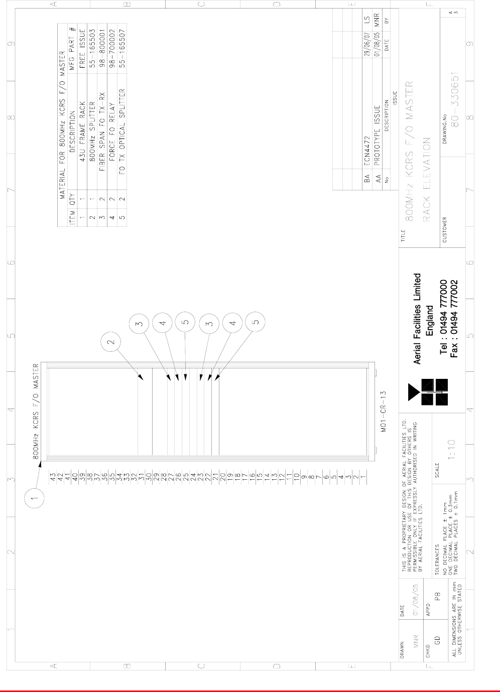
STTRS DOCUMENTATION
Document Number 80-330501HBKM – Issue A - Draft Page 19 of 500
4.1. 800MHz KCRS MASTER SITE (80-330651) Drawings
4.1.1. 800MHz KCRS MASTER SITE (80-330651) Rack Elevation
Drawing number 80-330651
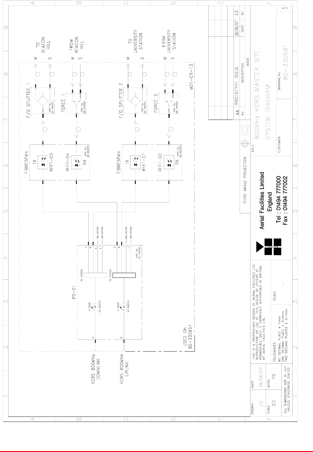
STTRS DOCUMENTATION
Document Number 80-330501HBKM – Issue A - Draft Page 20 of 500
4.1.2. 800MHz KCRS MASTER SITE (80-330651) System Diagram
Drawing number 80-330681
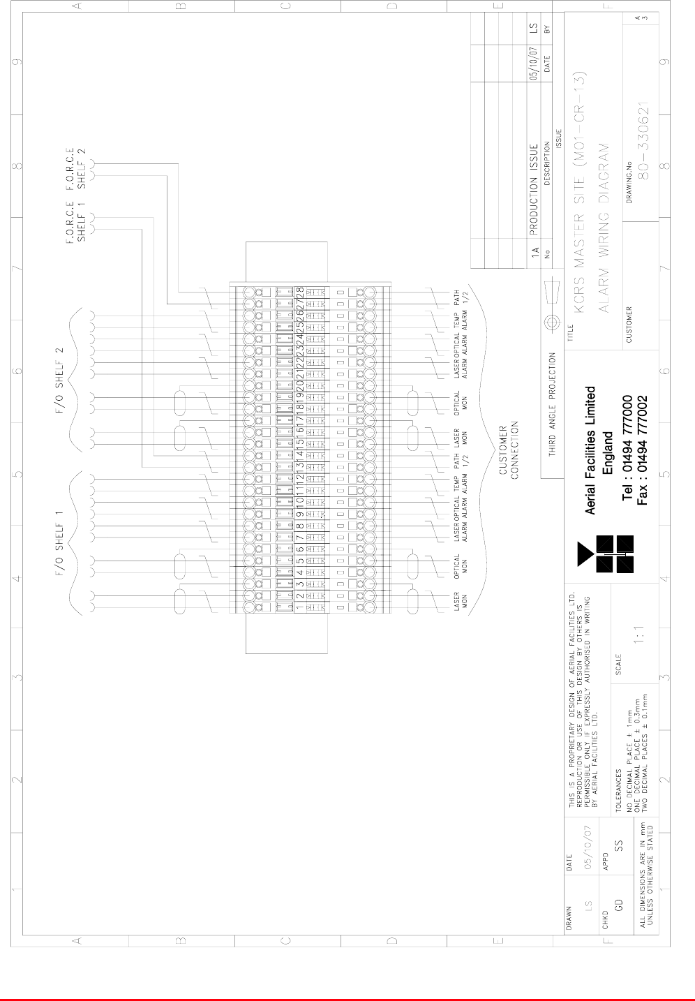
STTRS DOCUMENTATION
Document Number 80-330501HBKM – Issue A - Draft Page 21 of 500
4.1.3. 800MHz KCRS MASTER SITE (80-330651) Alarm Wiring Diagram
Drawing number 80-330621
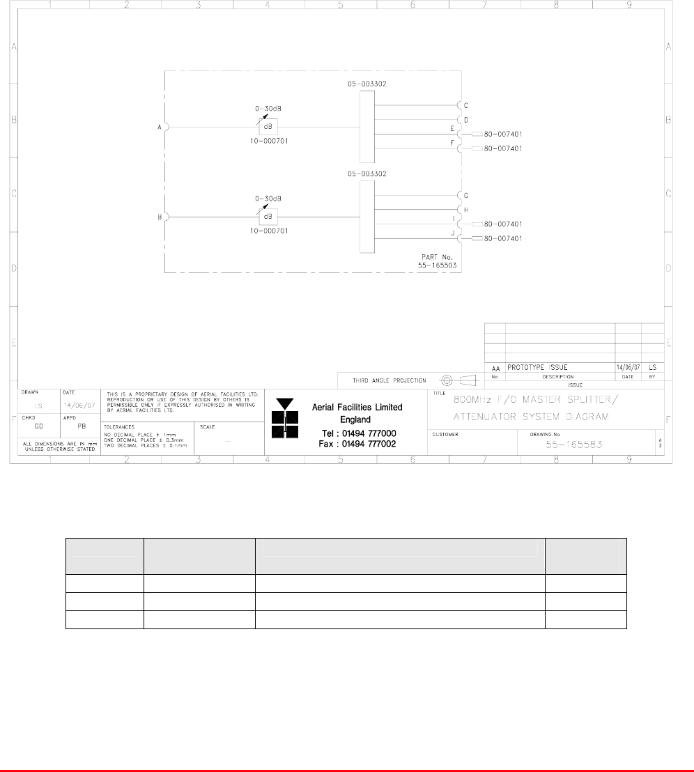
STTRS DOCUMENTATION
Document Number 80-330501HBKM – Issue A - Draft Page 22 of 500
4.2. 800MHz KCRS Master Site (80-330651) Sub Components
4.2.1. 800MHz FO Master Splitter/Attenuator (55-165503)
800MHz FO Master Splitter/Attenuator (55-165503) is a 2U rack mount tray which contains
attenuators and splitters.
The 800MHz KCRS Downlink passes through a switched attenuator (10-000701) before entering Four
Way Splitter/Combiner (05-003302) where the signal is split into two separate feeds for Beacon Hill
and University Station
In the Uplink path signals from Beacon Hill and University Station are combined by a second Four
Way Splitter/Combiner (05-003302) before passing through a switched attenuator (10-000701) then
exiting as the 800MHz KCRS Uplink
800MHz FO MASTER SPLITTER/ATTEN (55-165503) System Diagram
Drawing number 55-165583
800MHz FO Master Splitter/Attenuator (55-165503) List of Major Sub components
Section Component
Part Component Part Description Qty. Per
Assembly
4.2.1.1. 05-003302 Four Way Splitter/Combiner 2
4.2.1.2. 10-000701 Switched Attenuator 0.25Watt, 0 - 30dB 2
4.2.1.3. 80-007401 Dummy Load 4

STTRS DOCUMENTATION
Document Number 80-330501HBKM – Issue A - Draft Page 23 of 500
4.2.1.1. Four Way Splitter/Combiner (05-003302)
The Splitter/Combiner used is a device for accurately matching two or more RF signals to single or
multiple ports, whilst maintaining an accurate 50Ω load to all inputs/outputs and ensuring that the
VSWR and insertion losses are kept to a minimum. Any unused ports should be terminated with an
appropriate 50 load.
Four Way Splitter (05-003302) Specification
PARAMETER SPECIFICATION
Frequency range 700-980MHz
Bandwidth 180MHz
Rejection >14dB
Insertion loss <7.0dB (in band)
Connectors N type, female
Weight <1.5kg
operational -20%C to +60%C Temperature
range storage -40%C to +70%C
4.2.1.2. Switched Attenuator 0.25Watt, 0 - 30dB (10-000701)
In many practical applications for Cell Enhancers etc., the gain in each path is found to be excessive.
Therefore, provision is made within the unit for the setting of attenuation in each path, to reduce the
gain.
Switched Attenuator 10-000701 provides attenuation from 0 to 30dB in 2 dB steps The attenuation is
simply set using the four miniature toggle switches on the top of each unit. Each switch is clearly
marked with the attenuation it provides, and the total attenuation in line is the sum of the values
switched in. They are designed to maintain an accurate 50 impedance over their operating
frequency at both input and output.
10-000701 Specification
PARAMETER SPECIFICATION
Attenuation Values 0-30dB
Attenuation Steps 2, 4, 8 and 16dB
Power Handling 0.25 Watt
Attenuation Accuracy ± 1.0 dB
Frequency Range DC to 1GHz
Impedance 50
Connectors SMA
VSWR 1.3:1
Weight 0.2kg
operation -20°C to +60°C Temperature
range storage -40°C to +70°C

STTRS DOCUMENTATION
Document Number 80-330501HBKM – Issue A - Draft Page 24 of 500
4.2.1.3. Dummy Load (80-007401)
When a combiner system is used to split or combine RF signals, in many cases it is most cost
effective to use a standard stock item 4, 6 or 8 port device where, in fact, only a 3 or 6 port device is
needed. In this case the Four Way Splitters (05-003302) each have two of their ports terminated with
Dummy Load (80-007401) in order to preserve the correct impedance of the devices over the
specified frequency range. This also has the advantage of allowing future expansion capability should
extra channels or other functions become necessary.
Dummy Load (80-007401) Specification
Parameter Specification
Frequency Range 0 to 1000MHz
Power Rating 1.6 Watts
0-500MHz 1.2:1 VSWR
(Max) 500-1000MHz 1.3:1
Temperature -20 to +55°C
Connector ‘N’ type Male
Nominal Impedance 50 Ohms
4.2.2. F/O Link Subsystem (98-800001)
F/O Link Subsystem (98-800001) is an O.E.M. sourced Optical Tranceiver package containing
discreet TX and RX modules and supplied as a 1U rack mount tray
Parameter Specification
Optical Output Power 4 mW
Wavelength, peak 1310 1550 nm
Frequency Response, 50 to 2.2 GHz ± 1.5 dB
Input and Output VSWR 1.5:1
Link Gain (2) 0 dB
Output Noise Floor (1) -137 dBm/Hz
Input 3rd Order Intercept (1) 30 dBm
Operating Temperature 30 to +75°C
Storage Temperature 40 to +85°C
Maximum RF Input to Transmitter +20 dBm
Maximum Optical Input to Receiver 6 mW
A.C. Supply Voltage 90 – 265 VAC
Dimensions 483 x 457 x 44mm (19.0 x 18 x 1.72 in.)
(1) SFDR, Noise and IP3 specified with 5 dB optical loss.
(2) Link Gain specified with 1 meter fiber.
4.2.3. Optical A/B Switch FC/APC (98-700002)
Optical AB Switch FC/APC (98-700002)
Optical A/B Switch FC/APC (98-700002) an O.E.M. sourced Fibre Optic relay supplied as a 1U rack
mount tray. 98-700002 allows for the automatic switching between two optical inputs to provide a
common optical output. Manual selection of the input is also possible via toggle switches on the front
panel.

STTRS DOCUMENTATION
Document Number 80-330501HBKM – Issue A - Draft Page 25 of 500
98-700002 Specification
PARAMETER SPECIFICATION
Electrical Characteristics
Power Supply Voltage 100 - 240 VAC
Power Supply Frequency 50 - 60 Hz
Optical Characteristics
Operating Wavelength 1200 – 1610nm
Optical Input Range +20 dBm
Optical Insertion Loss 2.0 dB
Optical Trip Threshold/Meter Range -35 - +20 dBm
Optical Switch Speed 15ms
Backreflection Tolerance -50dB
Environmental and Physical Characteristics
Optical Connectors FC/APC
Operating Temp. Range +10 to +40°C
Storage Temp. Range -40 to +80 °C
Humidity 5 to 90 % RHNC
Weight 2.2 kg (6 lbs)
Dimensions 483 x 361 x 44mm (19.0 x 14.2 x 1.72 in.)
4.2.4. Fibre Optic Splitter (55-165507)
Fibre Optic Splitter (55-165507) is a 1U rack mount tray containing an optical splitter/coupler
Fibre Optic Splitter (55-165507) List of Major Sub Components
Component
Part Component Part Description Qty. Per
Assembly
98-100001 Single Mode Optical Splitter/Coupler 1
4.2.4.1. Single Mode Optical Splitter/Coupler (98-100001)
Single Mode Optical Splitter/Couplers are used whenever it is necessary to split or combine outputs
from optical transmitters or inputs to receivers. Operators should be aware that a small insertion loss
(typically 3-4dB) is common with these type of couplers.
Single Mode Optical Splitter/Coupler (98-100001) It is an O.E.M unit featuring almost negligible
insertion loss to the F/O signal. Extreme caution should be exercised when handling these devices.
Special attention should be shown to the connectors; repair of a broken Splitter/Coupler is not
possible; replacement is the only option.
In the two Fibre Optic Splitters (55-165507) in 800MHz KCRS Master Site (80-330651), Single Mode
Optical Splitter/Coupler (98-100001) is used to split the optical signal from the FO TX modules in F/O
Link Subsystem (98-700001) into two equal paths.

STTRS DOCUMENTATION
Document Number 80-330501HBKM – Issue A - Draft Page 26 of 500
5. 700MHz KCM MASTER SITE / PIONEER SQ (80-330652)
Description of 700MHz KCM MASTER SITE / PIONEER SQ (80-330652)
From the top of the rack
55-165703
55-165704
55-165703
55-165704
55-165604
98-800001
98-700002
55-165507
55-165708
700MHz KCM MASTER SITE / PIONEER SQ (80-330652) List of Major Sub Components
Section Component
Part Component Part Description Qty. Per
Assembly
5.4.1. 55-165703 800MHz LINE AMP + FILTERS (INT AMP) 2
5.4.2. 55-165704 700MHz LINE AMP + FILTERS (INT AMP) 2
5.4.3. 55-165604 700MHz FO MASTER ATTENUATOR 1
5.4.4. 98-800001 2GHz 1.5um F/O LINK SUBSYSTEM 1
5.4.5. 98-700002 OPTICAL A/B SWITCH FC/APC 1
5.4.6. 55-165507 FIBRE OPTIC SPLITTER 1
5.4.7. 55-165708 PIONEER ST. SPLITTER 1
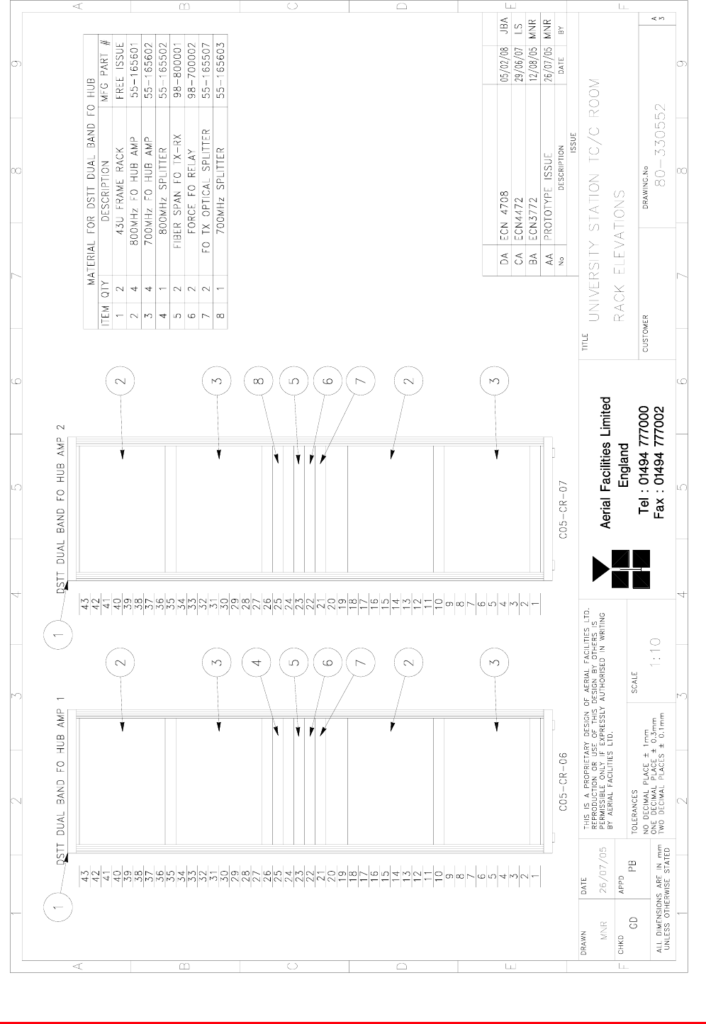
STTRS DOCUMENTATION
Document Number 80-330501HBKM – Issue A - Draft Page 27 of 500
5.1. 700MHz KCM MASTER SITE / PIONEER SQ (80-330652) Rack Elevation
Drawing number 80-330652
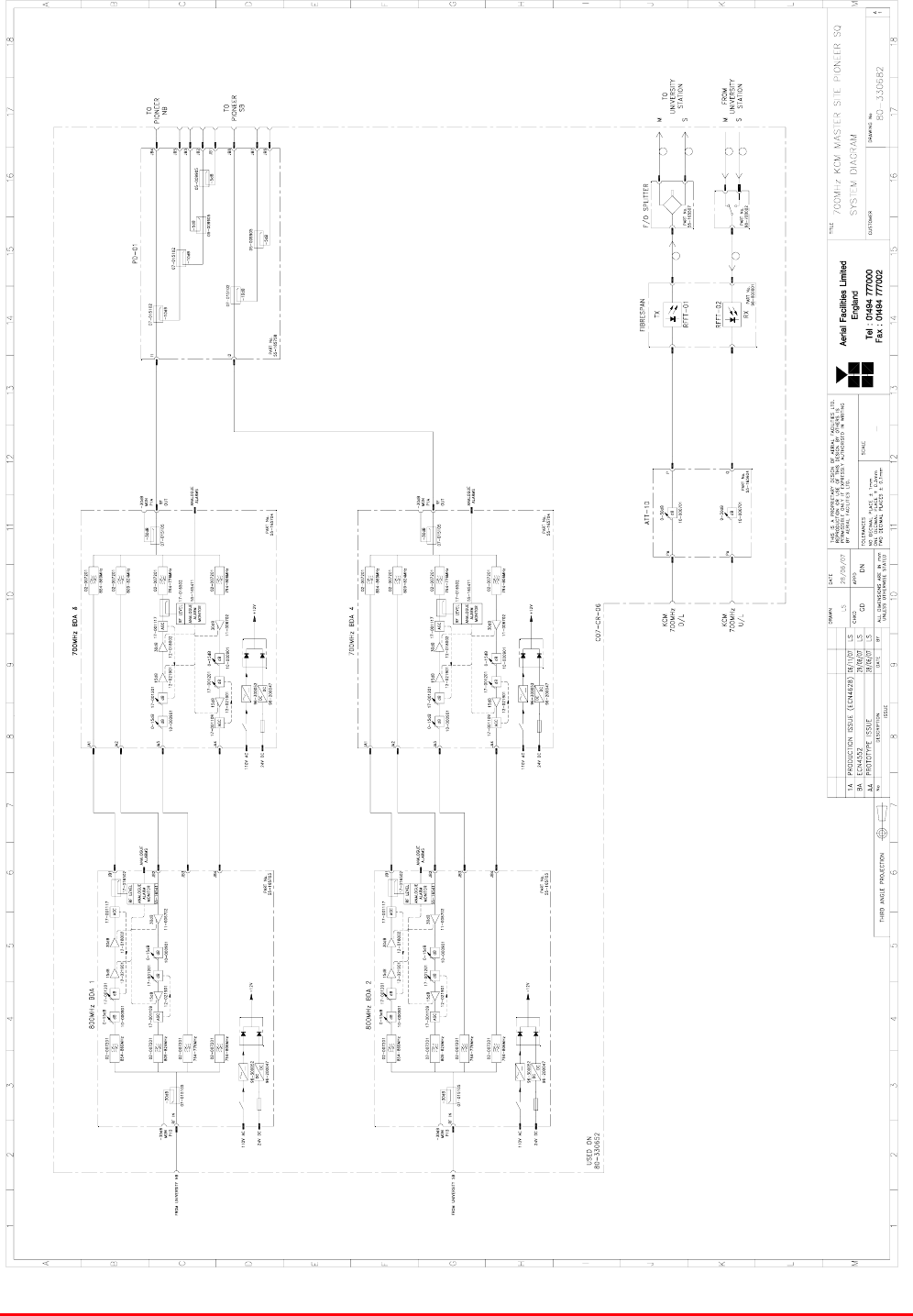
STTRS DOCUMENTATION
Document Number 80-330501HBKM – Issue A - Draft Page 28 of 500
5.2. 700MHz KCM MASTER SITE / PIONEER SQ (80-330682) System Diagram
Drawing number 80-330682

STTRS DOCUMENTATION
Document Number 80-330501HBKM – Issue A - Draft Page 29 of 500
5.3. 700MHz KCM MASTER SITE / PIONEER SQ (80-330682) Alarm Wiring Diagram
***//*** Approval In progresss G.D.
Drawing number 80-330622

STTRS DOCUMENTATION
Document Number 80-330501HBKM – Issue A - Draft Page 30 of 500
5.4. 700MHz KCM MASTER SITE / PIONEER SQ (80-330682) Sub Components
5.4.1. 800MHz Line Amplifier (55-165703)
800MHz Line Amplifier (55-165703) List of Major Components
Section Component
Part Component Part Description Qty. Per
Assembly
5.4.1.3. 02-007206 Bandpass Filter 4
5.4.1.4. 07-015105 Wideband Asymmetric Coupler 1
5.4.1.5. 10-000901 Switched Attenuator 0.25W, 0 - 15dB 2
5.4.1.6. 11-006702 Low Noise Amplifier 1
5.4.1.7. 12-018002 Power Amplifier (20W 800MHz ) 1
5.4.1.8. 12-021901 Low Power Amplifier 2
17-001109* AGC Detector Assembly (Logarithmic) 1
17-001117* AGC Detector Assembly 1
5.4.1.9.
17-001201* AGC Attenuator Assembly 2
5.4.1.10. 20-001601 12V (Dual) Relay Board 1
5.4.1.11. 80-008901 12V (Single) Relay Board 1
5.4.1.12. 94-100004 Dual Diode Assembly 1
5.4.1.13. 96-200047 DC/DC Converter 1
5.4.1.14. 96-300052 12V Switch-Mode PSU 1
*The sub components 17-001109, 17-001117 & 17-001201 are parts of the Automatic Gain Control
(AGC) system used in 800MHz Line Amplifier (55-165703); 17-001117 and 17-001201 are paired for
use in the uplink and 17-001109 and 17-001201 are paired for use in the downlink
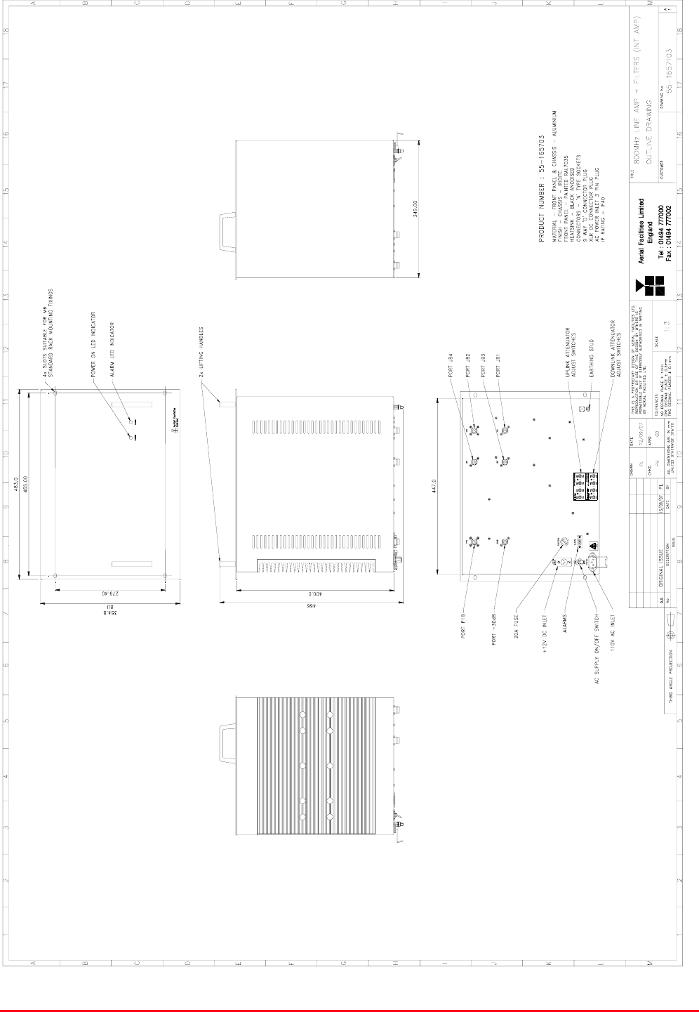
STTRS DOCUMENTATION
Document Number 80-330501HBKM – Issue A - Draft Page 31 of 500
5.4.1.1. 800MHz Line Amplifier (55-165703) Outline Drawing
Drawing number 55-1657103
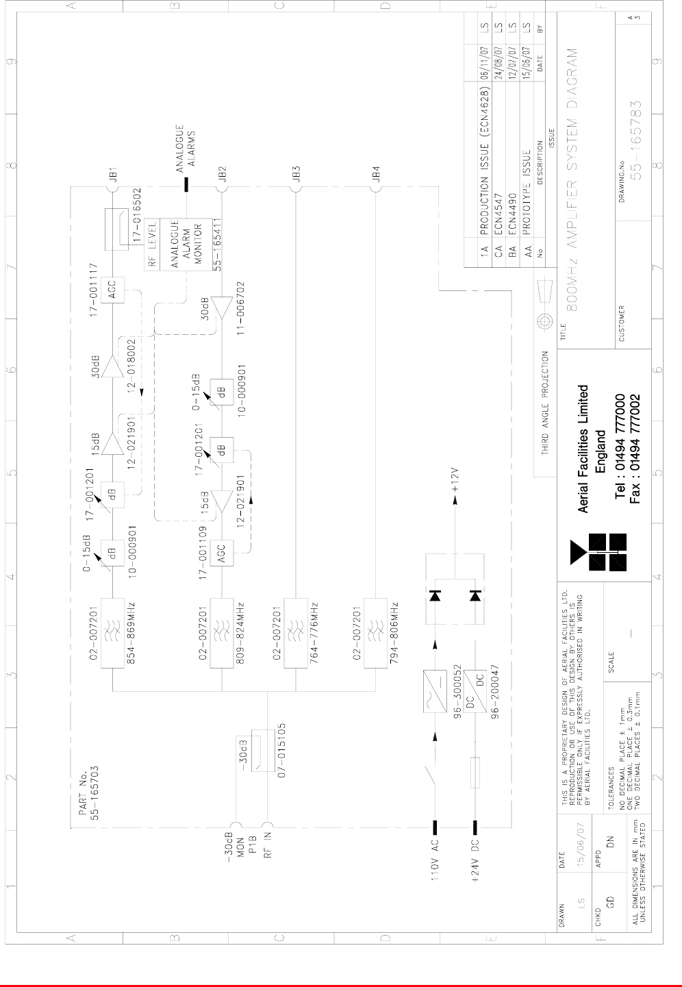
STTRS DOCUMENTATION
Document Number 80-330501HBKM – Issue A - Draft Page 32 of 500
5.4.1.2. 800MHz Line Amplifier (55-165703) System Diagram
Drawing number 55-165783

STTRS DOCUMENTATION
Document Number 80-330501HBKM – Issue A - Draft Page 33 of 500
5.4.1.3. Bandpass Filter (02-007206)
The bandpass filters are multi-section designs with a bandwidth dependent upon the passband
frequencies, (both tuned to customer requirements). The response shape is basically Chebyshev with
a passband design ripple of 0.1dB. The filters are of slot coupled, folded combline design, and are
carefully aligned during manufacture in order to optimise the insertion loss, VSWR and
intermodulation characteristics of the unit. The tuned elements are silver-plated to reduce surface
ohmic losses and maintain a good VSWR figure and 50 load at the input and output ports.
Being passive devices, the bandpass filters should have an extremely long operational life and require
no maintenance. Should a filter be suspect, it is usually most time efficient to replace the module
rather than attempt repair or re-tuning.
No adjustments should be attempted without full network sweep analysis facilities to monitor both
insertion loss and VSWR simultaneously.
02-007206 Specification
PARAMETER SPECIFICATION
Response type Chebyshev
Frequency range 800 - 950MHz *
Bandwidth 25MHz *
Number of sections 8
Insertion loss 1.2 dB
VSWR better than 1.2:1
Connectors SMA female
Power handling 100W max
operation -20°C to +60°C Temperature
range storage -40°C to +70°C
Weight 3 kg (typical) *tuned to Customer's specification
5.4.1.4. Wideband Asymmetric Coupler (07-015105)
The purpose of Wideband Asymmetric Coupler (07-015105) is to tap off a known portion (in this case
30dB) of RF signal from transmission lines and to combine them, for example through splitter units for
different purposes (alarms/monitoring etc.), whilst maintaining an accurate 50Ω load to all
ports/interfaces throughout the specified frequency range. They are known formally as directional
couplers as they couple power from the RF mainline in one direction only.
07-015105 Specification
PARAMETER SPECIFICATION
Construction Inductive air gap
Frequency 800-2500MHz
Through loss 0.4dB (typical)
Coupling level -30dB ±0.5dB
Isolation N/A
Weight <1.0kg
Connectors SMA, female
operation -20°C to +60°C
Temperature
range storage -40°C to +70°C
STTRS DOCUMENTATION
Document Number 80-330501HBKM – Issue A - Draft Page 34 of 500
5.4.1.5. Switched Attenuator 0.25W, 0 - 15dB (10-000901)
In many practical applications for Cell Enhancers etc., the gain in each path is found to be excessive.
Therefore, provision is made within the unit for the setting of attenuation in each path, to reduce the
gain.
10-000901 provides attenuation from 0 - 15dB in 2 dB steps The attenuation is simply set using the
four miniature toggle switches on the top of each unit. Each switch is clearly marked with the
attenuation it provides, and the total attenuation in line is the sum of the values switched in. They are
designed to maintain an accurate 50 impedance over their operating frequency at both input and
output.
10-000901 Specification
PARAMETER SPECIFICATION
Attenuation Values 0-15dB
Attenuation Steps 1, 2, 4 and 8dB
Power Handling 0.25 Watt
Attenuation Accuracy ± 1.0 dB
Frequency Range DC to 1GHz
Impedance 50
Connectors SMA
VSWR 1.3:1
Weigh 0.2kg
operation -20°C to +60°C Temperature
range storage -40°C to +70°C
5.4.1.6. Low Noise Amplifier (11-006702)
The Gallium-Arsenide low noise amplifiers used in 800MHz Line Amplifier (55-165703) are double
stage, solid-state low noise amplifiers. Class A circuitry is used throughout the units to ensure
excellent linearity and extremely low noise over a very wide dynamic range. The active devices are
very moderately rated to provide a long trouble-free working life. There are no adjustments on these
amplifiers, and in the unlikely event of a failure, then the complete amplifier should be replaced. This
amplifier features its own in-built alarm system which gives a volt-free relay contact type alarm that is
easily integrated into the main alarm system.
11-006702 Specification
PARAMETER SPECIFICATION
Frequency range: 800 – 1000MHz
Bandwidth: <200MHz
Gain: 29dB (typical)
1dB Compression point: 20dBm
OIP3: 33dBm
Input/Output return loss: >18dB
Noise figure: 1.3dB (typical)
Power consumption: 180mA @ 24V DC
Supply voltage: 10-24V DC
Connectors: SMA female
operational: -10°C to +60°C
Temperature range: storage: -20°C to +70°C
Size: 90 x 55 x 30.2mm
Weight: 290gms (approximately)
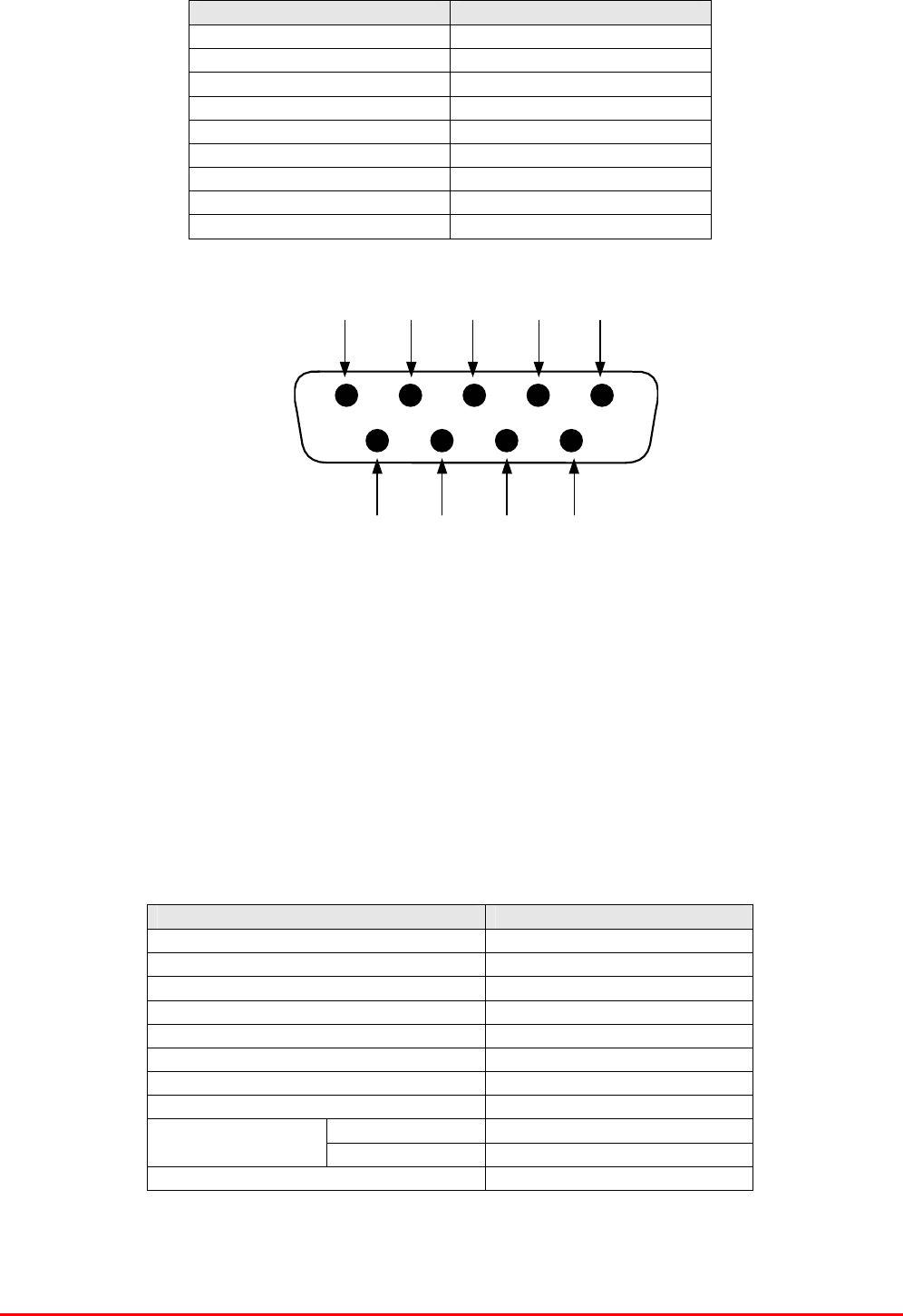
STTRS DOCUMENTATION
Document Number 80-330501HBKM – Issue A - Draft Page 35 of 500
7 8 96
1 2 3 4 5
9-Way Pin-Out Graphical Representation
Low Noise Amplifier (11-006702) ‘D’ Connector Pin-out details
Connector pin Signal
1 +Ve input (10-24V)
2 GND
3 Alarm RelayO/P bad
4 Alarm Relay common
5 Alarm Relay good
6 No connection
7 TTL voltage set
8 TTL alarm/0V (good)
9 O/C good/0V bad
5.4.1.7. Power Amplifier (12-018002)
This amplifier is a Class A 20W power amplifier from 800-960MHz in a 1 stage balanced
configuration. It demonstrates a very high linearity and a very good input/output return loss (RL). It
has built in a Current Fault Alarm Function.
Its housing is an aluminium case (Iridite NCP finish) with SMA connectors for the RF input/output and
a D-Type connector for the power supply and the Current Fault Alarm Function.
12-018002 Specification
PARAMETER SPECIFICATION
Frequency range: 800-960MHz
Small signal gain: 30dB
Gain flatness: ±1.2dB
I/O Return loss: >18dB
1dB compression point: 42.8dBm
OIP3: 56dBm
Supply voltage: 24V DC
Supply current: 5.0Amps (Typical)
operational: -10°C to +60°C Temperature
range storage: -20°C to +70°C
Weight: <2kg (no heatsink)
STTRS DOCUMENTATION
Document Number 80-330501HBKM – Issue A - Draft Page 36 of 500
Power Amplifier (12-018002) 7-Way Connector Pin-outs
Connector Pin Signal
A1 (large pin) +24V DC
A2 (large pin) GND
1 Alarm relay common
2 TTL alarm/0V good
3 Alarm relay contact (bad)
4 Alarm relay contact (good)
5 O/C good/0V bad (TTL)
5.4.1.8. Low Power Amplifier (12-021901)
The low power amplifier used is a triple stage solid-state low-noise amplifier. Class A circuitry is used
in the unit to ensure excellent linearity over a very wide dynamic range. The three active devices are
very moderately rated to provide a long trouble-free working life.
Its housing is an aluminium case (Iridite NCP finish) with SMA connectors for the RF input/output and
a D-Type connector for the power supply and the Current Fault Alarm Function.
There are no adjustments on this amplifier, and in the unlikely event of failure then the entire amplifier
should be replaced.
Low Power Amplifier (12-021901) Specification
PARAMETER SPECIFICATION
Frequency range 800-960MHz*
Bandwidth 20MHz *
Maximum RF output >1.0 Watt
Gain 15dB
1dB compression point +30.5dBm
3rd order intercept point +43dBm
Noise Figure <6dB
VSWR better than 1.5:1
Connectors SMA female
Supply 500mA @ 10-15V DC
operational -10°C to +60°C
Temperature
range storage -20°C to +70°C
Weight 0.5 kg
Size 167x52x25mm
* Tuned to Customer’s specification

STTRS DOCUMENTATION
Document Number 80-330501HBKM – Issue A - Draft Page 37 of 500
Low Power Amplifier (12-021901) 7-Way Connector Pin-outs
Connector Pin Signal
A1 (large pin) +24V DC
A2 (large pin) GND
1 Alarm relay common
2 TTL alarm/0V good
3 Alarm relay contact (bad)
4 Alarm relay contact (good)
5 O/C good/0V bad (TTL)
5.4.1.9. Automatic Gain Control
17-001109 AGC Detector Assembly (Logarithmic)
17-001117 AGC Detector Assembly
17-001201 AGC Attenuator Assembly
The sub components 17-001109, 17-001117 & 17-001201 are parts of the Automatic Gain Control
(AGC) system used in 800MHz Line Amplifier (55-165703); 17-001117 and 17-001201 are paired for
use in the uplink and 17-001109 and 17-001201 are paired for use in the downlink
800MHz Line Amplifier (55-165703) is fitted with two differing types of Automatic Gain Control (AGC)
system, one linear, and one logarithmic. The AGC with logarithmic detector (17-001117) is fitted in the
uplink path and the AGC with linear detector (17-001109) is fitted in the downlink path
The AFL Automatic Gain Control system consists of two units, a detector/amplifier and an attenuator.
The detector/amplifier unit is inserted in the RF path on the output of the power amplifier, and the
attenuator is situated in the RF path between the 1st and 2nd stages of amplification.
17-001117 and 17-001201 are paired for use in the uplink and 17-001109 and 17-001201 are paired
for use in the downlink
The attenuator comprises a 50 P.I.N diode, voltage-variable attenuator with a range of 3 to 30dB.
The attenuation is controlled by a DC voltage which is derived from the associated detector controller
board.
Normally the attenuator is at minimum attenuation. The detector/amplifier unit monitors the RF level
being delivered by the power amplifier, and when a certain threshold is reached it begins to increase
the value of the attenuator to limit the RF output to the (factory set) threshold. Therefore overloading
of the power amplifier is avoided.
The factory set threshold is 1dB below the Enhancer 1dB compression point. Some adjustment of this
AGC threshold level is possible, a 10dB range is mostly achieved. It is not recommended under any
circumstances to adjust the AGC threshold to a level greater than the 1dB compression point as
system degradation will occur.
STTRS DOCUMENTATION
Document Number 80-330501HBKM – Issue A - Draft Page 38 of 500
The detector comprises of a 50 transmission line with a resistive tap which samples a small portion
of the mainline power. The sampled signal is amplified and fed to a conventional half wave diode
rectifier, the output of which is a DC voltage proportional to the RF input signal.
This DC voltage is passed via an inverting DC amplifier with integrating characteristics, to the output,
which drives the attenuation control line of the corresponding AGC attenuator. This unit is fitted at
some earlier point in the RF circuit.
For small signals, below AGC onset, the output control line will be close to 12V and the AGC
attenuator will have minimum attenuation. As the signal level increases the control line voltage will
fall, increasing the attenuator value and keeping the system output level at a constant value.
AGC Specification (both types)
PARAMETER SPECIFICATION
Frequency range up to 1000MHz
Attenuation range 3 to 30dB
Attenuation steps continuously variable
VSWR better than 1.2:1
RF Connectors SMA female
attenuator 1W Power
handling detector/amp >30W (or as required)
operation -10°C to +60°C Temperature
range storage -20°C to +70°C
attenuator pcb 50 x 42 x 21mm
Size detector/amp pcb 54 x 42 x 21mm
attenuator 90grams
Weight detector/amp 100grams
5.4.1.10. 12V (Dual) Relay Board (20-001601)
The General Purpose Relay Board allows the inversion of signals and the isolation of circuits. It is
equipped with two dual pole change-over relays with completely isolated wiring, accessed via screw
terminals. Both relays are provided with polarity protection diodes and diodes for suppressing the
transients caused by "flywheel effect" which can destroy switching transistors or induce spikes on
neighbouring circuits. It’s common use is to amalgamate all the alarm signals into one, volts-free relay
contact pair for the main alarm system.
20-001601 Specification
PARAMETER SPECIFICATION
Operating voltage: 8 to 30V (floating earth)
Alarm threshold: Vcc - 1.20 volt +15%
Alarm output relay contacts:
Max. switch current: 1.0Amp
Max. switch volts: 120Vdc/60VA
Max. switch power: 24W/60VA
Min. switch load: 10.0µA/10.0mV
Relay isolation: 1.5kV
Mechanical life: >2x10⁷ operations
Relay approval: BT type 56
Connector details: Screw terminals
operational: -10°C to +60°C Temperature
range storage: -20°C to +70°C
STTRS DOCUMENTATION
Document Number 80-330501HBKM – Issue A - Draft Page 39 of 500
5.4.1.11. 12V (Single) Relay Board (80-008901)
The General Purpose Relay Board allows the inversion of signals and the isolation of circuits. It is
equipped with a single dual pole change-over relay RL1, with completely isolated wiring, accessed
via a 15 way in-line connector.
The relay is provided with polarity protection diodes and diodes for suppressing the transients caused
by "flywheel effect" which can destroy switching transistors or induce spikes on neighbouring circuits.
It’s common use is to amalgamate all the alarm signals into one, volts-free relay contact pair for the
main alarm system.
80-008901 Specification
PARAMETER SPECIFICATION
Operating voltage 8 to 30V (floating earth)
Alarm threshold Vcc - 1.20 volt +15%
Alarm output relay contacts:
Max. switch current 1.0Amp
Max. switch volts 120Vdc/60VA
Max. switch power 24W/60VA
Min. switch load 10.0µA/10.0mV
Relay isolation 1.5kV
Mechanical life >2x10⁷ operations
Relay approval BT type 56
Connector details Screw terminals
operational -10°C to +60°C Temperature
range storage -20°C to +70°C
5.4.1.12. Dual Diode Assembly (94-100004)
The purpose of these dual diode assemblies is to allow two DC voltage sources to be combined, so
that the main DC rail within the equipment can be sourced from either a mains driven PSU, or
externally through an XLR connector or from dual mains driven PSUs . They are very heavy-duty
diodes and they prevent any reverse current from flowing back to their source or the alternative
supply rail. Combining diodes such as these will also be used if the equipment is to be powered from
external back-up batteries.
5.4.1.13. DC/DC Converter 96-200047
96-200047 is an O.E.M. high power device with a wide input range and 12.5 amp @ 12V (150Watts)
output capability used to derive a 12V fixed voltage power supply rail from a higher voltage supply, in
this case 12V. In the event of failure this unit should not be repaired, only replaced.
PARAMETER SPECIFICATION
DC Input Voltage range 19 to 36V
DC Output voltage 12V ± 1%
Max. current load 12.5Amps
Operation -10°C to +60°C Temperature
range Storage -20°C to +85°C
Working Humidity 20 to 90% RHNC

STTRS DOCUMENTATION
Document Number 80-330501HBKM – Issue A - Draft Page 40 of 500
5.4.1.14. 12V Switch-Mode PSU (96-300052)
No routine maintenance of the PSU is required. If a fault is suspected, then the output voltage from
the power supply may be measured on its output terminals. This is typically set to 12.2V. The
adjustment potentiometer will be found close to the DC output terminals.
All the PSUs used in AFL Cell Enhancers are capable of operation from either 110 or 220V nominal
AC supplies. The line voltage is sensed automatically, so no adjustment or link setting is needed by
the operator.
96-300052 Specification
AC Input Supply 110 or 220V nominal
Voltage 85 - 265V AC
(absolute limits)
Frequency 47 to 63Hz
DC Output Supply 12V DC (nominal)
Voltage 10.5-13.8V (absolute limits)
Current 12.5A

STTRS DOCUMENTATION
Document Number 80-330501HBKM – Issue A - Draft Page 41 of 500
5.4.2 700MHz Line Amplifier (55-165704)
Description of 700MHz Line Amplifier (55-165704)
700MHz Line Amplifier (55-165704) List of Major Components
Section Component
Part Component Part Description Qty. Per
Assembly
5.4.2.3. 02-007206 Bandpass Filter 4
5.4.2.4. 07-015105 Wideband Asymmetric Coupler 1
5.4.2.5. 10-000901 Switched Attenuator 0.25W, 0 - 15dB 2
5.4.2.6. 11-006702 Low Noise Amplifier 1
5.4.2.7. 12-018002 Power Amplifier (20W 800MHz ) 1
5.4.2.8. 12-021901 Low Power Amplifier 2
17-001109* AGC Detector Assembly (Logarithmic) 1
17-001117* AGC Detector Assembly 1
5.4.2.9.
17-001201* AGC Attenuator Assembly 2
5.4.2.10. 80-008901 12V (Single) Relay Board 1
5.4.2.11. 94-100004 Dual Diode Assembly 1
5.4.2.12. 96-200047 DC/DC Converter 1
5.4.2.13. 96-300052 12V Switch-Mode PSU 1
*The sub components 17-001109, 17-001117 & 17-001201 are parts of the Automatic Gain Control
(AGC) system used in 800MHz Line Amplifier (55-165703); 17-001117 and 17-001201 are paired for
use in the uplink and 17-001109 and 17-001201 are paired for use in the downlink
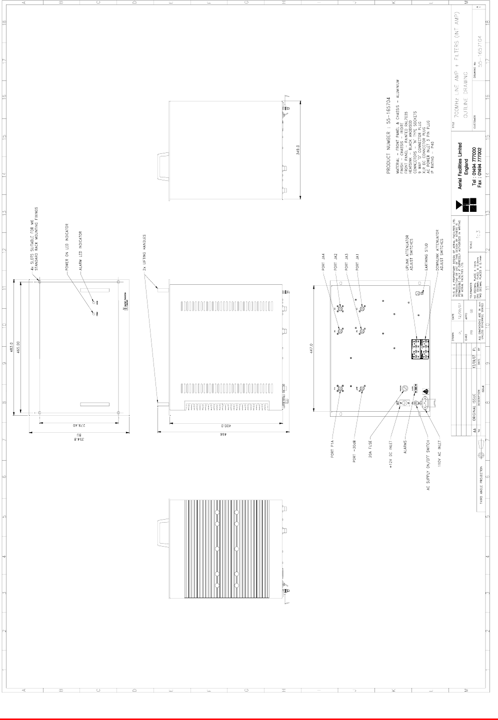
STTRS DOCUMENTATION
Document Number 80-330501HBKM – Issue A - Draft Page 42 of 500
5.4.2.1. 700MHz Line Amplifier (55-165704) Outline Drawing
Drawing number 55-1657104
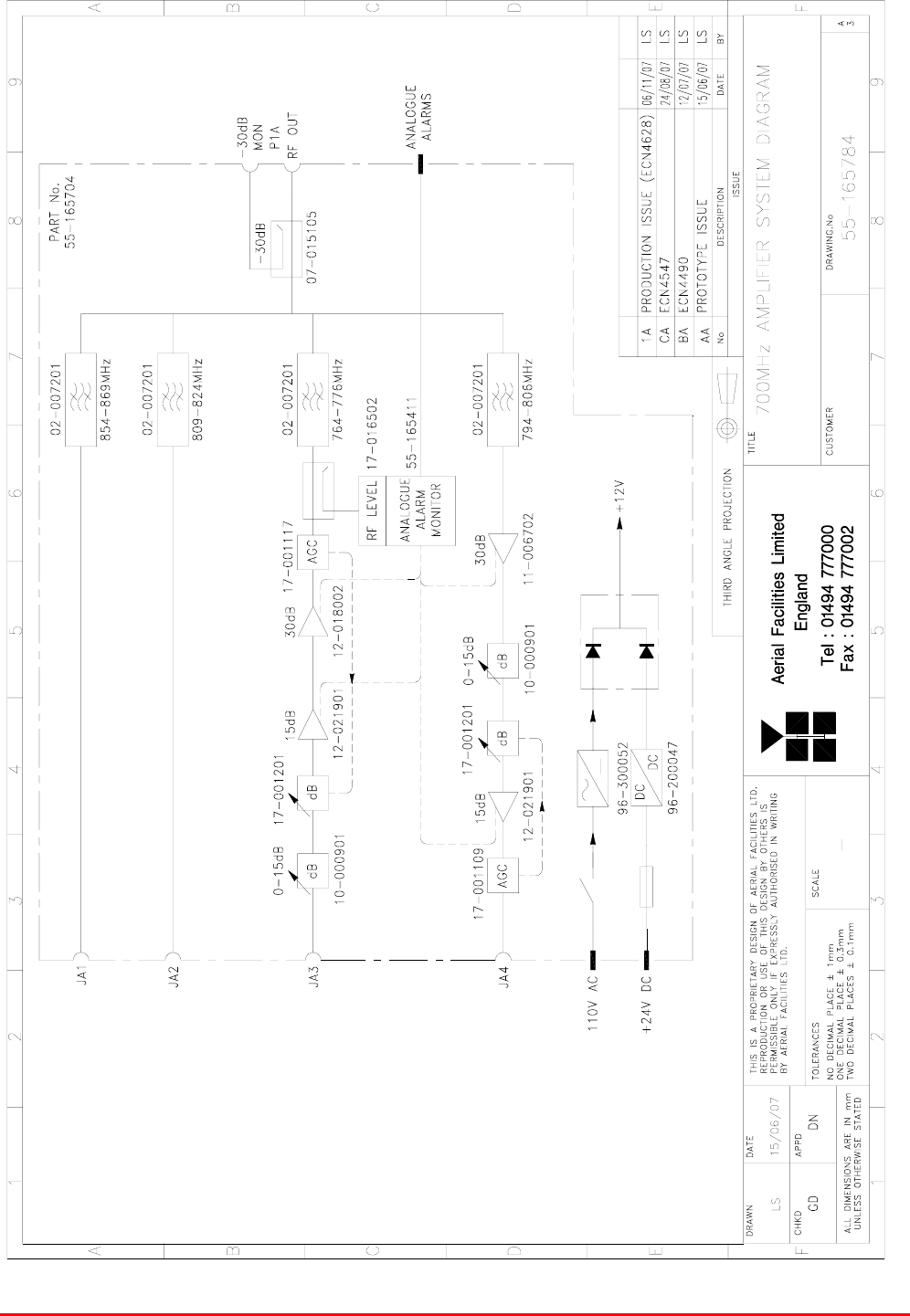
STTRS DOCUMENTATION
Document Number 80-330501HBKM – Issue A - Draft Page 43 of 500
5.4.2.2. 700MHz Line Amplifier (55-165704) System Diagram
Drawing number 55-165784
STTRS DOCUMENTATION
Document Number 80-330501HBKM – Issue A - Draft Page 44 of 500
5.4.2.3. Bandpass Filter (02-007206)
The bandpass filters are multi-section designs with a bandwidth dependent upon the passband
frequencies, (both tuned to customer requirements). The response shape is basically Chebyshev with
a passband design ripple of 0.1dB. The filters are of slot coupled, folded combline design, and are
carefully aligned during manufacture in order to optimise the insertion loss, VSWR and
intermodulation characteristics of the unit. The tuned elements are silver-plated to reduce surface
ohmic losses and maintain a good VSWR figure and 50 load at the input and output ports.
Being passive devices, the bandpass filters should have an extremely long operational life and require
no maintenance. Should a filter be suspect, it is usually most time efficient to replace the module
rather than attempt repair or re-tuning.
No adjustments should be attempted without full network sweep analysis facilities to monitor both
insertion loss and VSWR simultaneously.
02-007206 Specification
PARAMETER SPECIFICATION
Response type Chebyshev
Frequency range 800 - 950MHz *
Bandwidth 25MHz *
Number of sections 8
Insertion loss 1.2 dB
VSWR better than 1.2:1
Connectors SMA female
Power handling 100W max
operation -20°C to +60°C Temperature
range storage -40°C to +70°C
Weight 3 kg (typical) *tuned to Customer's specification
5.4.2.4. Wideband Asymmetric Coupler (07-015105)
The purpose of Wideband Asymmetric Coupler (07-015105) is to tap off a known portion (in this case
30dB) of RF signal from transmission lines and to combine them, for example through splitter units for
different purposes (alarms/monitoring etc.), whilst maintaining an accurate 50Ω load to all
ports/interfaces throughout the specified frequency range. They are known formally as directional
couplers as they couple power from the RF mainline in one direction only.
07-015105 Specification
PARAMETER SPECIFICATION
Construction Inductive air gap
Frequency 800-2500MHz
Through loss 0.4dB (typical)
Coupling level -30dB ±0.5dB
Isolation N/A
Weight <1.0kg
Connectors SMA, female
operation -20°C to +60°C
Temperature
range storage -40°C to +70°C

STTRS DOCUMENTATION
Document Number 80-330501HBKM – Issue A - Draft Page 45 of 500
5.4.2.5. Switched Attenuator 0.25W, 0 - 15dB (10-000901)
In many practical applications for Cell Enhancers etc., the gain in each path is found to be excessive.
Therefore, provision is made within the unit for the setting of attenuation in each path, to reduce the
gain.
10-000901 provides attenuation from 0 - 15dB in 2 dB steps The attenuation is simply set using the
four miniature toggle switches on the top of each unit. Each switch is clearly marked with the
attenuation it provides, and the total attenuation in line is the sum of the values switched in. They are
designed to maintain an accurate 50 impedance over their operating frequency at both input and
output.
10-000901 Specification
PARAMETER SPECIFICATION
Attenuation Values 0-15dB
Attenuation Steps 1, 2, 4 and 8dB
Power Handling 0.25 Watt
Attenuation Accuracy ± 1.0 dB
Frequency Range DC to 1GHz
Impedance 50
Connectors SMA
VSWR 1.3:1
Weigh 0.2kg
operation -20°C to +60°C Temperature
range storage -40°C to +70°C
5.4.2.6. Low Noise Amplifier (11-006702)
The Gallium-Arsenide low noise amplifiers used in 700MHz Line Amplifier (55-165704) are double
stage, solid-state low noise amplifiers. Class A circuitry is used throughout the units to ensure
excellent linearity and extremely low noise over a very wide dynamic range. The active devices are
very moderately rated to provide a long trouble-free working life. There are no adjustments on these
amplifiers, and in the unlikely event of a failure, then the complete amplifier should be replaced. This
amplifier features its own in-built alarm system which gives a volt-free relay contact type alarm that is
easily integrated into the main alarm system.
11-006702 Specification
PARAMETER SPECIFICATION
Frequency range: 800 – 1000MHz
Bandwidth: <200MHz
Gain: 29dB (typical)
1dB Compression point: 20dBm
OIP3: 33dBm
Input/Output return loss: >18dB
Noise figure: 1.3dB (typical)
Power consumption: 180mA @ 24V DC
Supply voltage: 10-24V DC
Connectors: SMA female
operational: -10°C to +60°C
Temperature range: storage: -20°C to +70°C
Size: 90 x 55 x 30.2mm
Weight: 290gms (approximately)

STTRS DOCUMENTATION
Document Number 80-330501HBKM – Issue A - Draft Page 46 of 500
7 8 96
1 2 3 4 5
9-Way Pin-Out Graphical Representation
Low Noise Amplifier (11-006702) ‘D’ Connector Pin-out details
Connector pin Signal
1 +Ve input (10-24V)
2 GND
3 Alarm RelayO/P bad
4 Alarm Relay common
5 Alarm Relay good
6 No connection
7 TTL voltage set
8 TTL alarm/0V (good)
9 O/C good/0V bad
5.4.2.7. Power Amplifier (12-018002)
This amplifier is a Class A 20W power amplifier from 800-960MHz in a 1 stage balanced
configuration. It demonstrates a very high linearity and a very good input/output return loss (RL). It
has built in a Current Fault Alarm Function.
Its housing is an aluminium case (Iridite NCP finish) with SMA connectors for the RF input/output and
a D-Type connector for the power supply and the Current Fault Alarm Function.
12-018002 Specification
PARAMETER SPECIFICATION
Frequency range: 800-960MHz
Small signal gain: 30dB
Gain flatness: ±1.2dB
I/O Return loss: >18dB
1dB compression point: 42.8dBm
OIP3: 56dBm
Supply voltage: 24V DC
Supply current: 5.0Amps (Typical)
operational: -10°C to +60°C Temperature
range storage: -20°C to +70°C
Weight: <2kg (no heatsink)
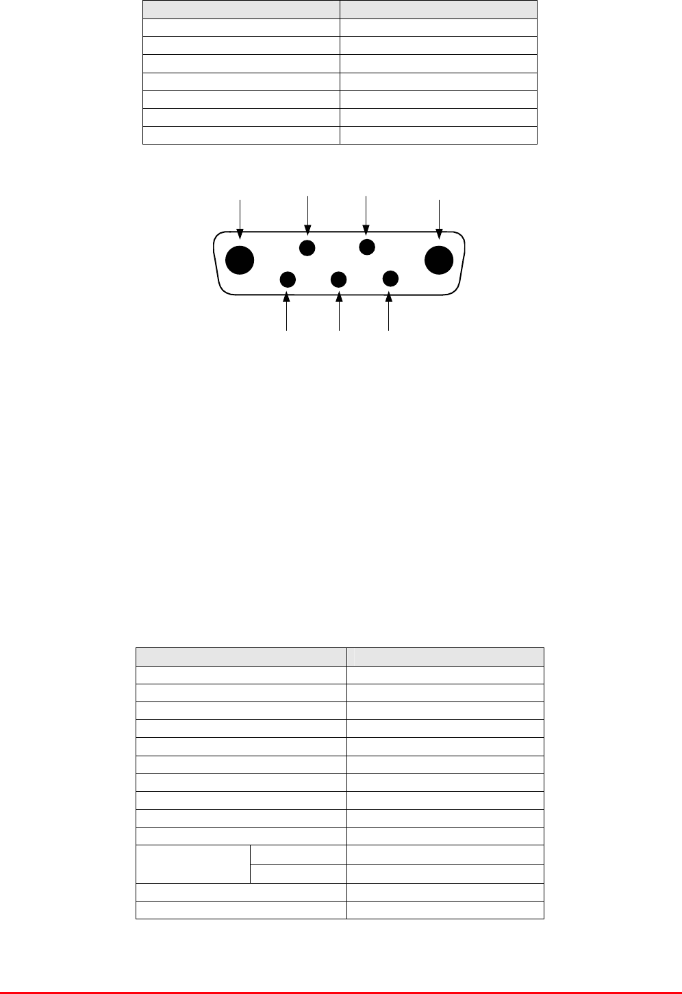
STTRS DOCUMENTATION
Document Number 80-330501HBKM – Issue A - Draft Page 47 of 500
Power Amplifier (12-018002) 7-Way Connector Pin-outs
Connector Pin Signal
A1 (large pin) +24V DC
A2 (large pin) GND
1 Alarm relay common
2 TTL alarm/0V good
3 Alarm relay contact (bad)
4 Alarm relay contact (good)
5 O/C good/0V bad (TTL)
5.4.2.8. Low Power Amplifier (12-021901)
The low power amplifier used is a triple stage solid-state low-noise amplifier. Class A circuitry is used
in the unit to ensure excellent linearity over a very wide dynamic range. The three active devices are
very moderately rated to provide a long trouble-free working life.
Its housing is an aluminium case (Iridite NCP finish) with SMA connectors for the RF input/output and
a D-Type connector for the power supply and the Current Fault Alarm Function.
There are no adjustments on this amplifier, and in the unlikely event of failure then the entire amplifier
should be replaced.
Low Power Amplifier (12-021901) Specification
PARAMETER SPECIFICATION
Frequency range 800-960MHz*
Bandwidth 20MHz *
Maximum RF output >1.0 Watt
Gain 15dB
1dB compression point +30.5dBm
3rd order intercept point +43dBm
Noise Figure <6dB
VSWR better than 1.5:1
Connectors SMA female
Supply 500mA @ 10-15V DC
operational -10°C to +60°C
Temperature
range storage -20°C to +70°C
Weight 0.5 kg
Size 167x52x25mm
* Tuned to Customer’s specification

STTRS DOCUMENTATION
Document Number 80-330501HBKM – Issue A - Draft Page 48 of 500
Low Power Amplifier (12-021901) 7-Way Connector Pin-outs
Connector Pin Signal
A1 (large pin) +24V DC
A2 (large pin) GND
1 Alarm relay common
2 TTL alarm/0V good
3 Alarm relay contact (bad)
4 Alarm relay contact (good)
5 O/C good/0V bad (TTL)
5.4.2.9. Automatic Gain Control
17-001109 AGC Detector Assembly (Logarithmic)
17-001117 AGC Detector Assembly
17-001201 AGC Attenuator Assembly
The sub components 17-001109, 17-001117 & 17-001201 are parts of the Automatic Gain Control
(AGC) system used in 700MHz Line Amplifier (55-165704); 17-001117 and 17-001201 are paired for
use in the uplink and 17-001109 and 17-001201 are paired for use in the downlink
700MHz Line Amplifier (55-165704) is fitted with two differing types of Automatic Gain Control (AGC)
system, one linear, and one logarithmic. The AGC with logarithmic detector (17-001117) is fitted in the
uplink path and the AGC with linear detector (17-001109) is fitted in the downlink path
The AFL Automatic Gain Control system consists of two units, a detector/amplifier and an attenuator.
The detector/amplifier unit is inserted in the RF path on the output of the power amplifier, and the
attenuator is situated in the RF path between the 1st and 2nd stages of amplification.
17-001117 and 17-001201 are paired for use in the uplink and 17-001109 and 17-001201 are paired
for use in the downlink
The attenuator comprises a 50 P.I.N diode, voltage-variable attenuator with a range of 3 to 30dB.
The attenuation is controlled by a DC voltage which is derived from the associated detector controller
board.
Normally the attenuator is at minimum attenuation. The detector/amplifier unit monitors the RF level
being delivered by the power amplifier, and when a certain threshold is reached it begins to increase
the value of the attenuator to limit the RF output to the (factory set) threshold. Therefore overloading
of the power amplifier is avoided.
The factory set threshold is 1dB below the Enhancer 1dB compression point. Some adjustment of this
AGC threshold level is possible, a 10dB range is mostly achieved. It is not recommended under any
circumstances to adjust the AGC threshold to a level greater than the 1dB compression point as
system degradation will occur.
STTRS DOCUMENTATION
Document Number 80-330501HBKM – Issue A - Draft Page 49 of 500
The detector comprises of a 50 transmission line with a resistive tap which samples a small portion
of the mainline power. The sampled signal is amplified and fed to a conventional half wave diode
rectifier, the output of which is a DC voltage proportional to the RF input signal.
This DC voltage is passed via an inverting DC amplifier with integrating characteristics, to the output,
which drives the attenuation control line of the corresponding AGC attenuator. This unit is fitted at
some earlier point in the RF circuit.
For small signals, below AGC onset, the output control line will be close to 12V and the AGC
attenuator will have minimum attenuation. As the signal level increases the control line voltage will
fall, increasing the attenuator value and keeping the system output level at a constant value.
AGC Specification (both types)
PARAMETER SPECIFICATION
Frequency range up to 1000MHz
Attenuation range 3 to 30dB
Attenuation steps continuously variable
VSWR better than 1.2:1
RF Connectors SMA female
attenuator 1W Power
handling detector/amp >30W (or as required)
operation -10°C to +60°C Temperature
range storage -20°C to +70°C
attenuator pcb 50 x 42 x 21mm
Size detector/amp pcb 54 x 42 x 21mm
attenuator 90grams
Weight detector/amp 100grams
5.4.2.10. 12V (Single) Relay Board (80-008901)
The General Purpose Relay Board allows the inversion of signals and the isolation of circuits. It is
equipped with a single dual pole change-over relay RL1, with completely isolated wiring, accessed
via a 15 way in-line connector.
The relay is provided with polarity protection diodes and diodes for suppressing the transients caused
by "flywheel effect" which can destroy switching transistors or induce spikes on neighbouring circuits.
It’s common use is to amalgamate all the alarm signals into one, volts-free relay contact pair for the
main alarm system.
80-008901 Specification PARAMETER SPECIFICATION
Operating voltage 8 to 30V (floating earth)
Alarm threshold Vcc - 1.20 volt +15%
Alarm output relay contacts:
Max. switch current 1.0Amp
Max. switch volts 120Vdc/60VA
Max. switch power 24W/60VA
Min. switch load 10.0µA/10.0mV
Relay isolation 1.5kV
Mechanical life >2x10⁷ operations
Relay approval BT type 56
Connector details Screw terminals
operational -10°C to +60°C Temperature
range storage -20°C to +70°C
STTRS DOCUMENTATION
Document Number 80-330501HBKM – Issue A - Draft Page 50 of 500
5.4.2.11. Dual Diode Assembly (94-100004)
The purpose of these dual diode assemblies is to allow two DC voltage sources to be combined, so
that the main DC rail within the equipment can be sourced from either a mains driven PSU, or
externally through an XLR connector or from dual mains driven PSUs . They are very heavy-duty
diodes and they prevent any reverse current from flowing back to their source or the alternative
supply rail. Combining diodes such as these will also be used if the equipment is to be powered from
external back-up batteries.
5.4.2.12. DC/DC Converter 96-200047
96-200047 is an O.E.M. high power device with a wide input range and 12.5 amp @ 12V (150Watts)
output capability used to derive a 12V fixed voltage power supply rail from a higher voltage supply, in
this case 12V. In the event of failure this unit should not be repaired, only replaced.
PARAMETER SPECIFICATION
DC Input Voltage range 19 to 36V
DC Output voltage 12V ± 1%
Max. current load 12.5Amps
Operation -10°C to +60°C Temperature
range Storage -20°C to +85°C
Working Humidity 20 to 90% RHNC
5.4.2.13. 12V Switch-Mode PSU (96-300052)
No routine maintenance of the PSU is required. If a fault is suspected, then the output voltage from
the power supply may be measured on its output terminals. This is typically set to 12.2V. The
adjustment potentiometer will be found close to the DC output terminals.
All the PSUs used in AFL Cell Enhancers are capable of operation from either 110 or 220V nominal
AC supplies. The line voltage is sensed automatically, so no adjustment or link setting is needed by
the operator.
96-300052 Specification
AC Input Supply 110 or 220V nominal
Voltage 85 - 265V AC
(absolute limits)
Frequency 47 to 63Hz
DC Output Supply 12V DC (nominal)
Voltage 10.5-13.8V (absolute limits)
Current 12.5A
STTRS DOCUMENTATION
Document Number 80-330501HBKM – Issue A - Draft Page 51 of 500
5.4.3. 700MHz FO MASTER ATTENUATOR (55-165604)
Description of 700MHz FO MASTER ATTENUATOR(55-165604)
700MHz FO MASTER ATTENUATOR(55-165604) List of Major Components
Component
Part Component Part Description Qty. Per
Assembly
10-000701 Switched Attenuator 0.25Watt, 0 - 30dB 2
5.4.3.1. Switched Attenuator 0.25Watt, 0 - 30dB (10-000701)
In many practical applications for Cell Enhancers etc., the gain in each path is found to be excessive.
Therefore, provision is made within the unit for the setting of attenuation in each path, to reduce the
gain.
Switched Attenuator 10-000701 provides attenuation from 0 to 30dB in 2 dB steps The attenuation is
simply set using the four miniature toggle switches on the top of each unit. Each switch is clearly
marked with the attenuation it provides, and the total attenuation in line is the sum of the values
switched in. They are designed to maintain an accurate 50 impedance over their operating
frequency at both input and output.
10-000701 Specification
PARAMETER SPECIFICATION
Attenuation Values 0-30dB
Attenuation Steps 2, 4, 8 and 16dB
Power Handling 0.25 Watt
Attenuation Accuracy ± 1.0 dB
Frequency Range DC to 1GHz
Impedance 50
Connectors SMA
VSWR 1.3:1
Weight 0.2kg
operation -20°C to +60°C Temperature
range storage -40°C to +70°C
STTRS DOCUMENTATION
Document Number 80-330501HBKM – Issue A - Draft Page 52 of 500
5.4.4. F/O Link Subsystem (98-800001)
F/O Link Subsystem (98-800001) is an O.E.M. sourced Optical Tranceiver package containing
discreet TX and RX modules and supplied as a 1U rack mount tray
Parameter Specification
Optical Output Power 4 mW
Wavelength, peak 1310 1550 nm
Frequency Response, 50 to 2.2 GHz ± 1.5 dB
Input and Output VSWR 1.5:1
Link Gain (2) 0 dB
Output Noise Floor (1) -137 dBm/Hz
Input 3rd Order Intercept (1) 30 dBm
Operating Temperature 30 to +75°C
Storage Temperature 40 to +85°C
Maximum RF Input to Transmitter +20 dBm
Maximum Optical Input to Receiver 6 mW
A.C. Supply Voltage 90 – 265 VAC
Dimensions 483 x 457 x 44mm (19.0 x 18 x 1.72 in.)
(1) SFDR, Noise and IP3 specified with 5 dB optical loss.
(2) Link Gain specified with 1 meter fiber.
5.4.5. Optical AB Switch FC/APC (98-700002)
Optical A/B Switch FC/APC (98-700002) an O.E.M. sourced Fibre Optic relay supplied as a 1U rack
mount tray. 98-700002 allows for the automatic switching between two optical inputs to provide a
common optical output. Manual selection of the input is also possible via toggle switches on the front
panel.
98-700002 Specification
PARAMETER SPECIFICATION
Electrical Characteristics
Power Supply Voltage 100 - 240 VAC
Power Supply Frequency 50 - 60 Hz
Optical Characteristics
Operating Wavelength 1200 – 1610nm
Optical Input Range +20 dBm
Optical Insertion Loss 2.0 dB
Optical Trip Threshold/Meter Range -35 - +20 dBm
Optical Switch Speed 15ms
Backreflection Tolerance -50dB
Environmental and Physical Characteristics
Optical Connectors FC/APC
Operating Temp. Range +10 to +40°C
Storage Temp. Range -40 to +80 °C
Humidity 5 to 90 % RHNC
Weight 2.2 kg (6 lbs)
Dimensions 483 x 361 x 44mm (19.0 x 14.2 x 1.72 in.)

STTRS DOCUMENTATION
Document Number 80-330501HBKM – Issue A - Draft Page 53 of 500
5.4.6. Fibre Optic Splitter (55-165507)
Fibre Optic Splitter (55-165507) is a 1U rack mount tray containing an optical splitter/coupler
Fibre Optic Splitter (55-165507) List of Major Sub Components
Component
Part Component Part Description Qty. Per
Assembly
98-100001 Single Mode Optical Splitter/Coupler 1
5.4.6.1. Single Mode Optical Splitter/Coupler (98-100001)
Single Mode Optical Splitter/Couplers are used whenever it is necessary to split or combine outputs
from optical transmitters or inputs to receivers. Operators should be aware that a small insertion loss
(typically 3-4dB) is common with these type of couplers.
Single Mode Optical Splitter/Coupler (98-100001) It is an O.E.M unit featuring almost negligible
insertion loss to the F/O signal. Extreme caution should be exercised when handling these devices.
Special attention should be shown to the connectors; repair of a broken Splitter/Coupler is not
possible; replacement is the only option.
In the Fibre Optic Splitter (55-165507) in 700MHZ KCM Master Site / Pioneer Sq. (80-330652), Single
Mode Optical Splitter/Coupler (98-100001) is used to split the optical signal from the FO TX module in
F/O Link Subsystem (98-700001) into two equal paths.
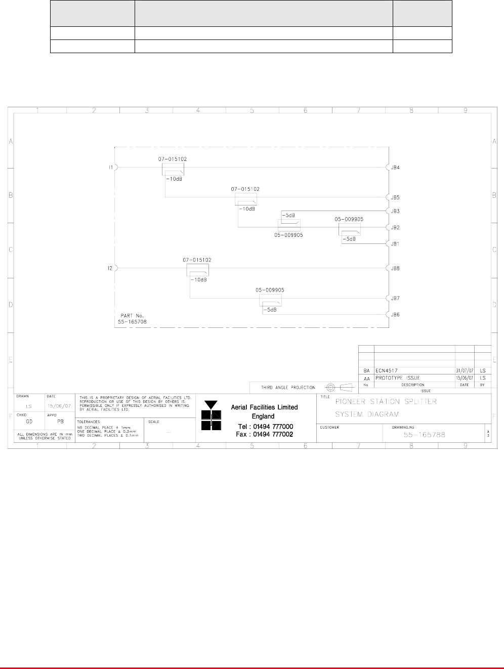
STTRS DOCUMENTATION
Document Number 80-330501HBKM – Issue A - Draft Page 54 of 500
5.4.7. PIONEER ST. SPLITTER (55-165708)
PIONEER ST. SPLITTER (55-165708) List of major Components
Component
Part Component Part Description Qty. Per
Assembly
05-009905 2 Way Power Splitter/Combiner 70/30 3
07-015102 Wideband Asymmetric Coupler 3
PIONEER ST. SPLITTER (55-165708) System Diagram
Drawing number 55-165788

STTRS DOCUMENTATION
Document Number 80-330501HBKM – Issue A - Draft Page 55 of 500
5.4.7.1. 2 Way Power Splitter/ Combiner 70/30 (05-009905)
The power Splitter/Combiner is a device for accurately matching two or more RF signals to single or
multiple ports, whilst maintaining an accurate 50Ω load to all inputs/outputs and ensuring that the
VSWR, return and insertion losses are kept to a minimum. Any unused ports will be terminated with
an appropriate 50Ω load. Power devices such as these, typically give 10dB better output isolation
than low power equivalents – (important for splitters that feed antenna systems).
05-009905 Specification
Specification Parameter
Frequency Range 764 – 860MHz
Impedence 50
Insertion Loss ± 0.3dB
VSWR 1.25:1
Splitter 100Watts Maximum
input power Combiner 5Watts
Power splitting/combining ratio 70% - 30%
RF Connectors N Female
Dimensions 104mm x 63mm x 46mm
operation: -20°C to +60°C Temperature
range storage: -40°C to +70°C
5.4.7.2. Wideband Asymmetric Coupler (07-015102)
The purpose of Wideband Asymmetric Coupler (07-015102) is to tap off a known portion (in this case
10dB) of RF signal from transmission lines and to combine them, for example through splitter units for
different purposes (alarms/monitoring etc.), whilst maintaining an accurate 50Ω load to all
ports/interfaces throughout the specified frequency range. They are known formally as directional
couplers as they couple power from the RF mainline in one direction only.
07-015102 Specification
PARAMETER SPECIFICATION
Frequency Range 800 - 2500 MHz
Coupling Value 10 dB ± 1.0 dB
Main Line Insertion Loss <1.6 dB
VSWR 1.4:1
Directivity >18 dB
Power Rating 200 Watts
RF Connectors ‘N’ female
operation -20°C to +60°C
Temperature
range storage -40°C to +70°C

STTRS DOCUMENTATION
Document Number 80-330501HBKM – Issue A - Draft Page 56 of 500
6. BEACON HILL STATION MASTER SITE 1 (80-330551-1)
Cabinet number C19-CR-05
from top of rack
55-165504
55-165501
55-165501
55-165502
98-800001
98-700002
55-165507
Beacon Hill Station Master Site 1 (80-330551-1) List of major Components
Section
Component
Part Component Part Description Qty. Per
Assembly
6.3.1. 55-165501 800MHz FO HUB AMP 2
6.3.2. 55-165502 800MHz FO HUB SPLITTER/COMB 1
6.3.3. 55-165504 BEACON HILL SPLITTER (BDA 1 & 3) 1
6.3.4. 55-165507 FIBRE OPTIC SPLITTER 1
6.3.5. 98-700002 OPTICAL A/B SWITCH FC/APC 1
6.3.6. 98-800001 2GHz 1.5um F/O LINK SUBSYSTEM 1
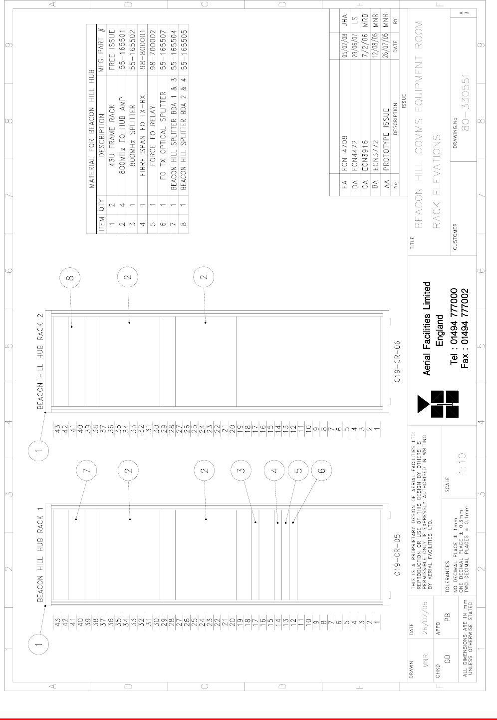
STTRS DOCUMENTATION
Document Number 80-330501HBKM – Issue A - Draft Page 57 of 500
6.1. Beacon Hill Station Master Site 1 (80-330551-1) Rack Elevation
Drawing number 80-330551
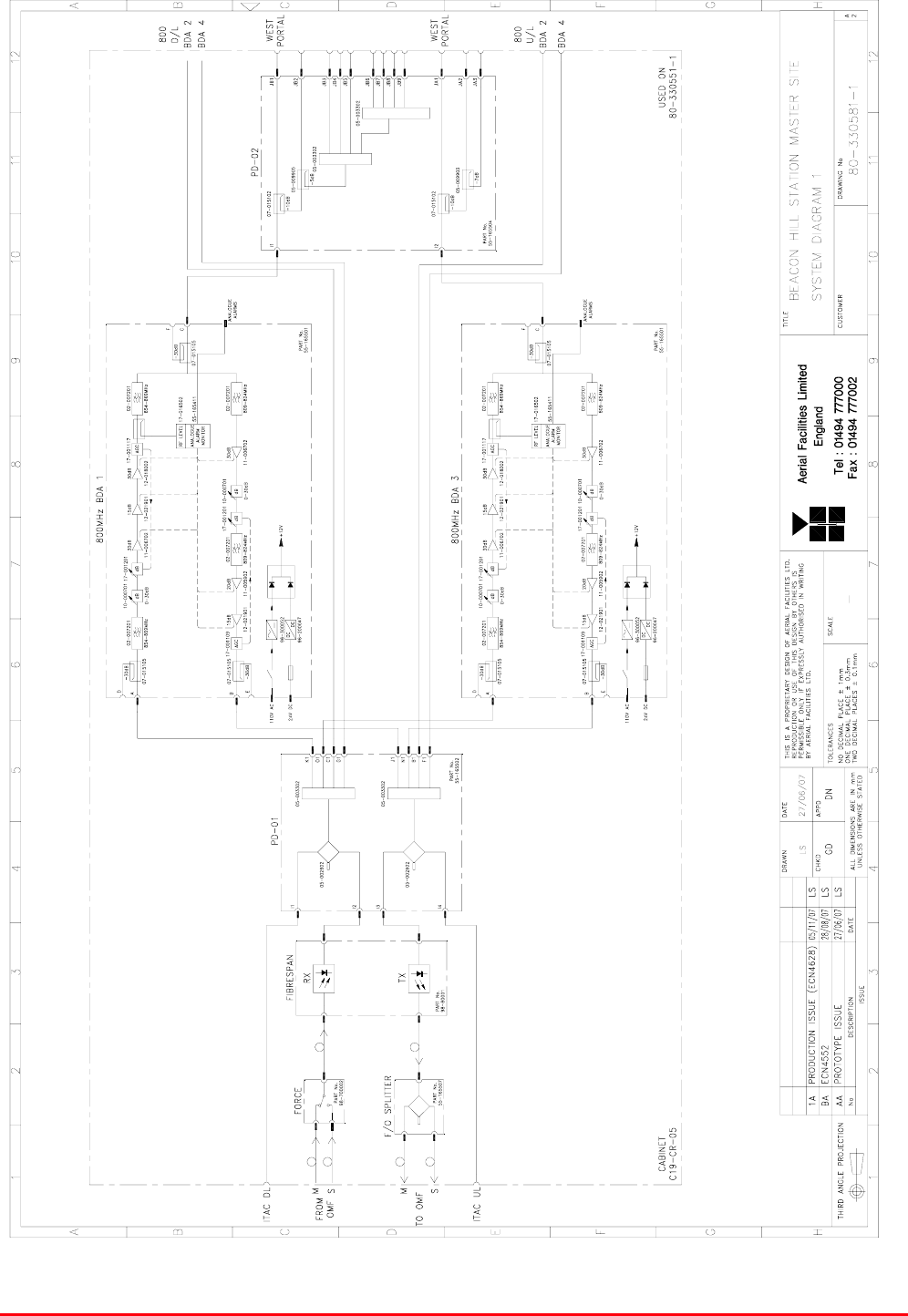
STTRS DOCUMENTATION
Document Number 80-330501HBKM – Issue A - Draft Page 58 of 500
6.2. Beacon Hill Station Master Site 1 (80-330551-1) System Diagram
Drawing number 80-330581-1

STTRS DOCUMENTATION
Document Number 80-330501HBKM – Issue A - Draft Page 59 of 500
Beacon Hill Station Master Site 1 (80-330551-1) Alarm Wiring Diagram ***///***
Approval In Progress G.D.
Drawing number 80-330521-1

STTRS DOCUMENTATION
Document Number 80-330501HBKM – Issue A - Draft Page 60 of 500
6.3. Beacon Hill Station Master Site 1 (80-330551-1) Sub Components
6.3.1. 800MHz FO HUB AMP (55-165501)
800MHz FO HUB AMP (55-165501) List of major components
Section Component
Part Component Part Description Qty. Per
Assembly
6.3.1.3. 02-007206 Bandpass Filter 4
6.3.1.4. 07-015105 Wideband Asymmetric Coupler 3
6.3.1.5. 10-000701 Switched Attenuator 0.25Watt, 0 - 30dB 2
6.3.1.6. 11-005902 Low Noise Amplifier 1
6.3.1.7. 11-006702 Low Noise Amplifier 2
6.3.1.8. 12-018002 Power Amplifier 1
6.3.1.9. 12-021901 Low Power Amplifier 2
17-001109* AGC Detector Assembly (Logarithmic) 1
17-001117* AGC Detector Assembly 1
6.3.1.10.
17-001201* AGC Attenuator Assembly 2
6.3.1.11. 20-001601 12V (Dual) Relay Board 1
6.3.1.12. 80-008901 12V (Single) Relay Board 1
6.3.1.13. 94-100004 Dual Diode Assembly 1
6.3.1.14. 96-200047 DC/DC Converter
6.3.1.15. 96-300052 12V Switch-Mode PSU 1
*The sub components 17-001109, 17-001117 & 17-001201 are parts of the Automatic Gain Control
(AGC) system used in 800MHz FO HUB AMP (55-165501); 17-001117 and 17-001201 are paired for
use in the uplink and 17-001109 and 17-001201 are paired for use in the downlink
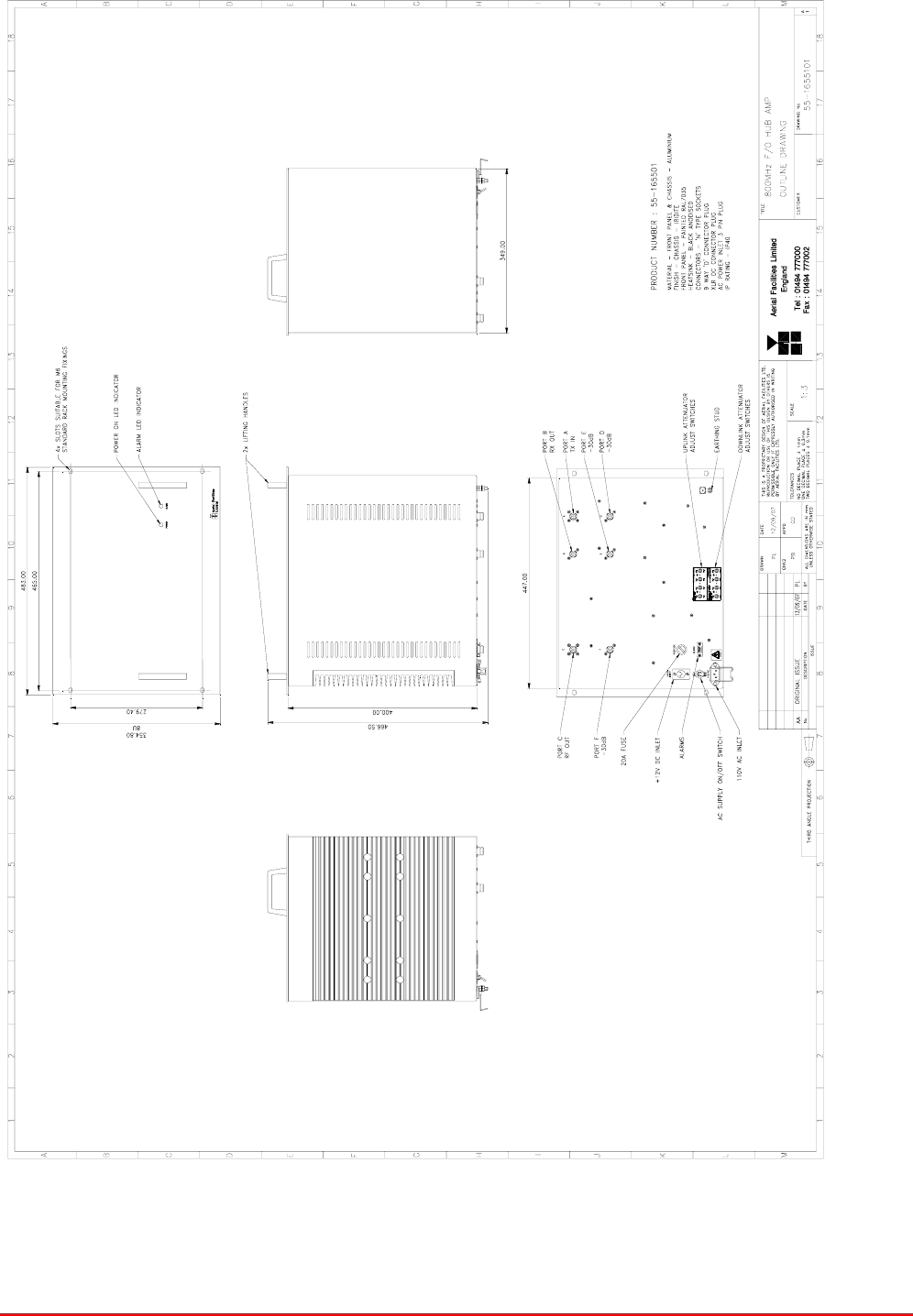
STTRS DOCUMENTATION
Document Number 80-330501HBKM – Issue A - Draft Page 61 of 500
6.3.1.1. 800MHz FO HUB AMP (55-165501) Outline drawing
Drawing number 55-1655101
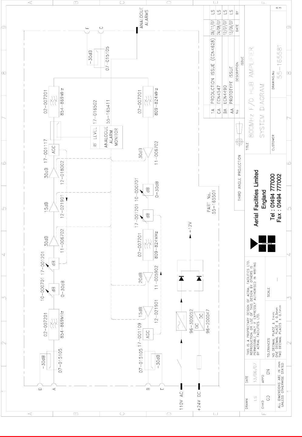
STTRS DOCUMENTATION
Document Number 80-330501HBKM – Issue A - Draft Page 62 of 500
6.3.1.2. 800MHz FO HUB AMP (55-165501) System Diagram
Drawing number 55-165581

STTRS DOCUMENTATION
Document Number 80-330501HBKM – Issue A - Draft Page 63 of 500
6.3.1.3. Bandpass Filter (02-007206)
The bandpass filters are multi-section designs with a bandwidth dependent upon the passband
frequencies, (both tuned to customer requirements). The response shape is basically Chebyshev with
a passband design ripple of 0.1dB. The filters are of slot coupled, folded combline design, and are
carefully aligned during manufacture in order to optimise the insertion loss, VSWR and
intermodulation characteristics of the unit. The tuned elements are silver-plated to reduce surface
ohmic losses and maintain a good VSWR figure and 50 load at the input and output ports.
Being passive devices, the bandpass filters should have an extremely long operational life and require
no maintenance. Should a filter be suspect, it is usually most time efficient to replace the module
rather than attempt repair or re-tuning.
No adjustments should be attempted without full network sweep analysis facilities to monitor both
insertion loss and VSWR simultaneously.
02-007206 Specification
PARAMETER SPECIFICATION
Response type Chebyshev
Frequency range 800 - 950MHz *
Bandwidth 25MHz *
Number of sections 8
Insertion loss 1.2 dB
VSWR better than 1.2:1
Connectors SMA female
Power handling 100W max
operation -20°C to +60°C Temperature
range storage -40°C to +70°C
Weight 3 kg (typical) *tuned to Customer's specification
6.3.1.4. Wideband Asymmetric Coupler (07-015105)
The purpose of Wideband Asymmetric Coupler (07-015105) is to tap off a known portion (in this case
30dB) of RF signal from transmission lines and to combine them, for example through splitter units for
different purposes (alarms/monitoring etc.), whilst maintaining an accurate 50Ω load to all
ports/interfaces throughout the specified frequency range. They are known formally as directional
couplers as they couple power from the RF mainline in one direction only.
07-015105 Specification
PARAMETER SPECIFICATION
Construction Inductive air gap
Frequency 800-2500MHz
Through loss 0.4dB (typical)
Coupling level -30dB ±0.5dB
Isolation N/A
Weight <1.0kg
Connectors SMA, female
operation -20°C to +60°C
Temperature
range storage -40°C to +70°C

STTRS DOCUMENTATION
Document Number 80-330501HBKM – Issue A - Draft Page 64 of 500
6.3.1.5. Switched Attenuator 0.25Watt, 0 - 30dB (10-000701)
In many practical applications for Cell Enhancers etc., the gain in each path is found to be excessive.
Therefore, provision is made within the unit for the setting of attenuation in each path, to reduce the
gain.
Switched Attenuator 10-000701 provides attenuation from 0 to 30dB in 2 dB steps The attenuation is
simply set using the four miniature toggle switches on the top of each unit. Each switch is clearly
marked with the attenuation it provides, and the total attenuation in line is the sum of the values
switched in. They are designed to maintain an accurate 50 impedance over their operating
frequency at both input and output.
10-000701 Specification
PARAMETER SPECIFICATION
Attenuation Values 0-30dB
Attenuation Steps 2, 4, 8 and 16dB
Power Handling 0.25 Watt
Attenuation Accuracy ± 1.0 dB
Frequency Range DC to 1GHz
Impedance 50
Connectors SMA
VSWR 1.3:1
Weight 0.2kg
operation -20°C to +60°C Temperature
range storage -40°C to +70°C
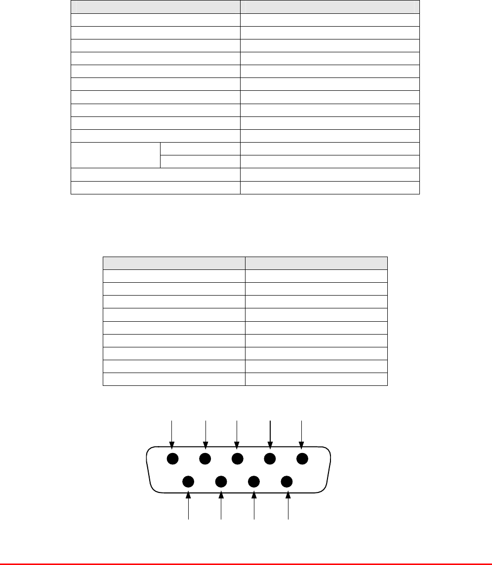
STTRS DOCUMENTATION
Document Number 80-330501HBKM – Issue A - Draft Page 65 of 500
6.3.1.6. Low Noise Amplifier (11-005902)
The Gallium-Arsenide low noise amplifier used in the unit is a double stage, solid-state low noise
amplifier. Class A circuitry is used throughout the units to ensure excellent linearity and extremely low
noise over a very wide dynamic range. The active devices are very moderately rated to provide a long
trouble-free working life. There are no adjustments on these amplifiers, and in the unlikely event of a
failure, then the complete amplifier should be replaced. This amplifier features its own in-built alarm
system which gives a volt-free relay contact type alarm that is easily integrated into any alarm system.
There is a Current Fault Alarm Function, which indicates failure of each one or both RF transistors by
a various alarm output options. The amplifier is housed in an aluminium case (Iridite NCP finish) with
SMA connectors for the RF input/output and a 9way D-type for DC and alarm outputs.
11-005902 Specification
PARAMETER SPECIFICATION
Frequency range: 800 – 960MHz *
Bandwidth: <170MHz
Gain: 19.5dB (typical)
1dB compression point: 21dBm
OIP3: 33dBm
Input/output return loss: >20dB
Noise figure: 1dB (typical)
Power consumption: 190mA @ 24V DC
Supply voltage: 10-24V DC
Connectors: SMA female
operational: -10°C to +60°C Temperature
range storage: -40°C to +70°C
Size: 90 x 55 x 30.2mm
Weight: 0.28kg *tuned to Customer's specification
LNA ‘D’ Connector Pin-out details
Connector pin Signal
1 +Ve input (10-24V)
2 GND
3 Alarm relay O/P bad
4 Alarm relay common
5 Alarm relay good
6 No connection
7 TTL voltage set
8 TTL alarm/0V (good)
9 O/C good/0V bad

STTRS DOCUMENTATION
Document Number 80-330501HBKM – Issue A - Draft Page 66 of 500
7 8 96
1 2 3 4 5
9-Way Pin-Out Graphical Representation
6.3.1.7. Low Noise Amplifier (11-006702)
The Gallium-Arsenide low noise amplifiers used in 800MHz Line Amplifier (55-165703) are double
stage, solid-state low noise amplifiers. Class A circuitry is used throughout the units to ensure
excellent linearity and extremely low noise over a very wide dynamic range. The active devices are
very moderately rated to provide a long trouble-free working life. There are no adjustments on these
amplifiers, and in the unlikely event of a failure, then the complete amplifier should be replaced. This
amplifier features its own in-built alarm system which gives a volt-free relay contact type alarm that is
easily integrated into the main alarm system.
11-006702 Specification
PARAMETER SPECIFICATION
Frequency range 800 – 1000MHz
Bandwidth <200MHz
Gain 29dB (typical)
1dB Compression point 20dBm
OIP3 33dBm
Input/Output return loss >18dB
Noise figure 1.3dB (typical)
Power consumption 180mA @ 24V DC
Supply voltage 10-24V DC
Connectors SMA female
operational -10°C to +60°C
Temperature range: storage -20°C to +70°C
Size 90 x 55 x 30.2mm
Weight 290gms (approximately)
Low Noise Amplifier (11-006702) ‘D’ Connector Pin-out details
Connector pin Signal
1 +Ve input (10-24V)
2 GND
3 Alarm RelayO/P bad
4 Alarm Relay common
5 Alarm Relay good
6 No connection
7 TTL voltage set
8 TTL alarm/0V (good)
9 O/C good/0V bad

STTRS DOCUMENTATION
Document Number 80-330501HBKM – Issue A - Draft Page 67 of 500
6.3.1.8. Power Amplifier (12-018002)
This amplifier is a Class A 20W power amplifier from 800-960MHz in a 1 stage balanced
configuration. It demonstrates a very high linearity and a very good input/output return loss (RL). It
has built in a Current Fault Alarm Function.
Its housing is an aluminium case (Iridite NCP finish) with SMA connectors for the RF input/output and
a D-Type connector for the power supply and the Current Fault Alarm Function.
12-018002 Specification
PARAMETER SPECIFICATION
Frequency range 800-960MHz
Small signal gain 30dB
Gain flatness ±1.2dB
I/O Return loss >18dB
1dB compression point 42.8dBm
OIP3 56dBm
Supply voltage 24V DC
Supply current 5.0Amps (Typical)
operational -10°C to +60°C Temperature
range storage -20°C to +70°C
Weight <2kg (no heatsink)
Power Amplifier (12-018002) 7-Way Connector Pin-outs
Connector Pin Signal
A1 (large pin) +24V DC
A2 (large pin) GND
1 Alarm relay common
2 TTL alarm/0V good
3 Alarm relay contact (bad)
4 Alarm relay contact (good)
5 O/C good/0V bad (TTL)
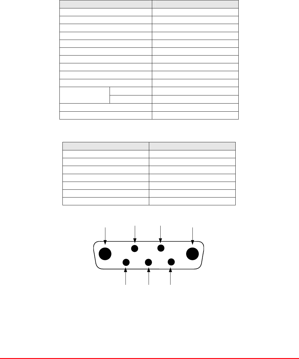
STTRS DOCUMENTATION
Document Number 80-330501HBKM – Issue A - Draft Page 68 of 500
6.3.1.9. Low Power Amplifier (12-021901)
The low power amplifier used is a triple stage solid-state low-noise amplifier. Class A circuitry is used
in the unit to ensure excellent linearity over a very wide dynamic range. The three active devices are
very moderately rated to provide a long trouble-free working life.
Its housing is an aluminium case (Iridite NCP finish) with SMA connectors for the RF input/output and
a D-Type connector for the power supply and the Current Fault Alarm Function.
There are no adjustments on this amplifier, and in the unlikely event of failure then the entire amplifier
should be replaced.
Low Power Amplifier (12-021901) Specification
PARAMETER SPECIFICATION
Frequency range 800-960MHz*
Bandwidth 20MHz *
Maximum RF output >1.0 Watt
Gain 15dB
1dB compression point +30.5dBm
3rd order intercept point +43dBm
Noise Figure <6dB
VSWR better than 1.5:1
Connectors SMA female
Supply 500mA @ 10-15V DC
operational -10°C to +60°C
Temperature
range storage -20°C to +70°C
Weight 0.5 kg
Size 167x52x25mm
* Tuned to Customer’s specification
Low Power Amplifier (12-021901) 7-Way Connector Pin-outs
Connector Pin Signal
A1 (large pin) +24V DC
A2 (large pin) GND
1 Alarm relay common
2 TTL alarm/0V good
3 Alarm relay contact (bad)
4 Alarm relay contact (good)
5 O/C good/0V bad (TTL)

STTRS DOCUMENTATION
Document Number 80-330501HBKM – Issue A - Draft Page 69 of 500
6.3.1.10. Automatic Gain Control
17-001109 AGC Detector Assembly (Logarithmic)
17-001117 AGC Detector Assembly
17-001201 AGC Attenuator Assembly
The sub components 17-001109, 17-001117 & 17-001201 are parts of the Automatic Gain Control
(AGC) system used in 800MHz FO HUB AMP (55-165501); 17-001117 and 17-001201 are paired for
use in the uplink and 17-001109 and 17-001201 are paired for use in the downlink
800MHz FO HUB AMP (55-165501) is fitted with two differing types of Automatic Gain Control (AGC)
system, one linear, and one logarithmic. The AGC with logarithmic detector (17-001117) is fitted in the
uplink path and the AGC with linear detector (17-001109) is fitted in the downlink path
The AFL Automatic Gain Control system consists of two units, a detector/amplifier and an attenuator.
The detector/amplifier unit is inserted in the RF path on the output of the power amplifier, and the
attenuator is situated in the RF path between the 1st and 2nd stages of amplification.
17-001117 and 17-001201 are paired for use in the uplink and 17-001109 and 17-001201 are paired
for use in the downlink
The attenuator comprises a 50 P.I.N diode, voltage-variable attenuator with a range of 3 to 30dB.
The attenuation is controlled by a DC voltage which is derived from the associated detector controller
board.
Normally the attenuator is at minimum attenuation. The detector/amplifier unit monitors the RF level
being delivered by the power amplifier, and when a certain threshold is reached it begins to increase
the value of the attenuator to limit the RF output to the (factory set) threshold. Therefore overloading
of the power amplifier is avoided.
The factory set threshold is 1dB below the Enhancer 1dB compression point. Some adjustment of this
AGC threshold level is possible, a 10dB range is mostly achieved. It is not recommended under any
circumstances to adjust the AGC threshold to a level greater than the 1dB compression point as
system degradation will occur.
The detector comprises of a 50 transmission line with a resistive tap which samples a small portion
of the mainline power. The sampled signal is amplified and fed to a conventional half wave diode
rectifier, the output of which is a DC voltage proportional to the RF input signal.
This DC voltage is passed via an inverting DC amplifier with integrating characteristics, to the output,
which drives the attenuation control line of the corresponding AGC attenuator. This unit is fitted at
some earlier point in the RF circuit.
For small signals, below AGC onset, the output control line will be close to 12V and the AGC
attenuator will have minimum attenuation. As the signal level increases the control line voltage will
fall, increasing the attenuator value and keeping the system output level at a constant value.

STTRS DOCUMENTATION
Document Number 80-330501HBKM – Issue A - Draft Page 70 of 500
AGC Specification (both types)
PARAMETER SPECIFICATION
Frequency range up to 1000MHz
Attenuation range 3 to 30dB
Attenuation steps continuously variable
VSWR better than 1.2:1
RF Connectors SMA female
attenuator 1W Power
handling detector/amp >30W (or as required)
operation -10°C to +60°C Temperature
range storage -20°C to +70°C
attenuator pcb 50 x 42 x 21mm
Size detector/amp pcb 54 x 42 x 21mm
attenuator 90grams
Weight detector/amp 100grams
6.3.1.11. 12V (Dual) Relay Board (20-001601)
The General Purpose Relay Board allows the inversion of signals and the isolation of circuits. It is
equipped with two dual pole change-over relays with completely isolated wiring, accessed via screw
terminals. Both relays are provided with polarity protection diodes and diodes for suppressing the
transients caused by "flywheel effect" which can destroy switching transistors or induce spikes on
neighbouring circuits. It’s common use is to amalgamate all the alarm signals into one, volts-free relay
contact pair for the main alarm system.
20-001601 Specification
PARAMETER SPECIFICATION
Operating voltage: 8 to 30V (floating earth)
Alarm threshold: Vcc - 1.20 volt +15%
Alarm output relay contacts:
Max. switch current: 1.0Amp
Max. switch volts: 120Vdc/60VA
Max. switch power: 24W/60VA
Min. switch load: 10.0µA/10.0mV
Relay isolation: 1.5kV
Mechanical life: >2x10⁷ operations
Relay approval: BT type 56
Connector details: Screw terminals
operational: -10°C to +60°C Temperature
range storage: -20°C to +70°C

STTRS DOCUMENTATION
Document Number 80-330501HBKM – Issue A - Draft Page 71 of 500
6.3.1.12. 12V (Single) Relay Board (80-008901)
The General Purpose Relay Board allows the inversion of signals and the isolation of circuits. It is
equipped with a single dual pole change-over relay RL1, with completely isolated wiring, accessed
via a 15 way in-line connector.
The relay is provided with polarity protection diodes and diodes for suppressing the transients caused
by "flywheel effect" which can destroy switching transistors or induce spikes on neighbouring circuits.
It’s common use is to amalgamate all the alarm signals into one, volts-free relay contact pair for the
main alarm system.
80-008901 Specification
PARAMETER SPECIFICATION
Operating voltage 8 to 30V (floating earth)
Alarm threshold Vcc - 1.20 volt +15%
Alarm output relay contacts:
Max. switch current 1.0Amp
Max. switch volts 120Vdc/60VA
Max. switch power 24W/60VA
Min. switch load 10.0µA/10.0mV
Relay isolation 1.5kV
Mechanical life >2x10⁷ operations
Relay approval BT type 56
Connector details Screw terminals
operational -10°C to +60°C Temperature
range storage -20°C to +70°C
6.3.1.13. Dual Diode Assembly (94-100004)
The purpose of these dual diode assemblies is to allow two DC voltage sources to be combined, so
that the main DC rail within the equipment can be sourced from either a mains driven PSU, or
externally through an XLR connector or from dual mains driven PSUs. They are very heavy-duty
diodes and they prevent any reverse current from flowing back to their source or the alternative
supply rail. Combining diodes such as these will also be used if the equipment is to be powered from
external back-up batteries.

STTRS DOCUMENTATION
Document Number 80-330501HBKM – Issue A - Draft Page 72 of 500
6.3.1.14. DC/DC Converter 96-200047
96-200047 is an O.E.M. high power device with a wide input range and 12.5 amp @ 12V (150Watts)
output capability used to derive a 12V fixed voltage power supply rail from a higher voltage supply, in
this case 12V. In the event of failure this unit should not be repaired, only replaced.
PARAMETER SPECIFICATION
DC Input Voltage range 19 to 36V
DC Output voltage 12V ± 1%
Max. current load 12.5Amps
Operation -10°C to +60°C Temperature
range Storage -20°C to +85°C
Working Humidity 20 to 90% RHNC
6.3.1.15. 12V Switch-Mode PSU (96-300052)
No routine maintenance of the PSU is required. If a fault is suspected, then the output voltage from
the power supply may be measured on its output terminals. This is typically set to 12.2V. The
adjustment potentiometer will be found close to the DC output terminals.
All the PSUs used in AFL Cell Enhancers are capable of operation from either 110 or 220V nominal
AC supplies. The line voltage is sensed automatically, so no adjustment or link setting is needed by
the operator.
96-300052 Specification
AC Input Supply 110 or 220V nominal
Voltage 85 - 265V AC (absolute limits)
Frequency 47 to 63Hz
DC Output Supply 12V DC (nominal)
Voltage 10.5-13.8V (absolute limits)
Current 12.5A

STTRS DOCUMENTATION
Document Number 80-330501HBKM – Issue A - Draft Page 73 of 500
6.3.2. 800MHz FO HUB SPLITTER/COMB (55-165502)
800MHz FO HUB SPLITTER/COMB (55-165502) List of major components
Section Component
Part Component Part Description Qty. Per
Assembly
6.3.2.3. 05-002602 900MHZ SPLITTER/COMBINER, 20W 2
6.3.2.4. 05-003302 Four Way Splitter/Combiner 2
STTRS DOCUMENTATION
Document Number 80-330501HBKM – Issue A - Draft Page 74 of 500
6.3.2.1. 800MHz FO HUB SPLITTER/COMB (55-165502) Outline Drawing
Drawing number 55-1655102
STTRS DOCUMENTATION
Document Number 80-330501HBKM – Issue A - Draft Page 75 of 500
6.3.2.2. 800MHz FO HUB SPLITTER/COMB (55-165502) System Diagram
Drawing number 55-165582
STTRS DOCUMENTATION
Document Number 80-330501HBKM – Issue A - Draft Page 76 of 500
6.3.2.3. 900MHz Splitter/Combiner (05-002602)
The Splitter/Combiner used is a device for accurately matching two or more RF signals to single or
multiple ports, whilst maintaining an accurate 50Ω load to all inputs/outputs and ensuring that the
VSWR and insertion losses are kept to a minimum. Any unused ports should be terminated with an
appropriate 50Ω load.
Being passive devices, the splitters should have an extremely long operational life and require no
maintenance. Should a unit be suspect, it is usually most time efficient to replace the whole module
rather than attempt repair or re-tuning.
05-002602 Specification
PARAMETER SPECIFICATION
Narrowband 815 – 960MHz Frequency
range Broadband 800 – 1200MHz
Narrowband 145MHz
Bandwidth Broadband 400MHz
Input ports 1
Output ports 2
Narrowband 3.3dB
Insertion loss Broadband 3.5dB
Return loss input & output 1.3:1
Impedance 50
Narrowband >20dB
Isolation Broadband >18dB
MTFB >180,000 hours
Splitting 20Watts
Power rating Combining 0.5Watt
Connectors SMA female
Weight 200g (approximately)
Size 54 x 44 x 21mm
6.3.2.4. Four Way Splitter/Combiner (05-003302)
The Splitter/Combiner used is a device for accurately matching two or more RF signals to single or
multiple ports, whilst maintaining an accurate 50Ω load to all inputs/outputs and ensuring that the
VSWR and insertion losses are kept to a minimum. Any unused ports should be terminated with an
appropriate 50 load.
Four Way Splitter (05-003302) Specification
PARAMETER SPECIFICATION
Frequency range 700-980MHz
Bandwidth 180MHz
Rejection >14dB
Insertion loss <7.0dB (in band)
Connectors N type, female
Weight <1.5kg
operational -20%C to +60%C Temperature
range storage -40%C to +70%C

STTRS DOCUMENTATION
Document Number 80-330501HBKM – Issue A - Draft Page 77 of 500
6.3.3. BEACON HILL SPLITTER (BDA 1 & 3) (55-165504)
BEACON HILL SPLITTER (BDA 1 & 3) (55-165504) List of major Components
Section
Component
Part Component Part Description Qty. Per
Assembly
6.3.3.3. 05-003302 Four Way Splitter/Combiner 2
6.3.3.4. 05-009903 2 Way Power Splitter/ Combiner 80/20 1
6.3.3.5. 05-009905 2 Way Power Splitter/ Combiner 70/30, 1
6.3.3.6. 07-015102 Wideband Asymmetric Coupler 2
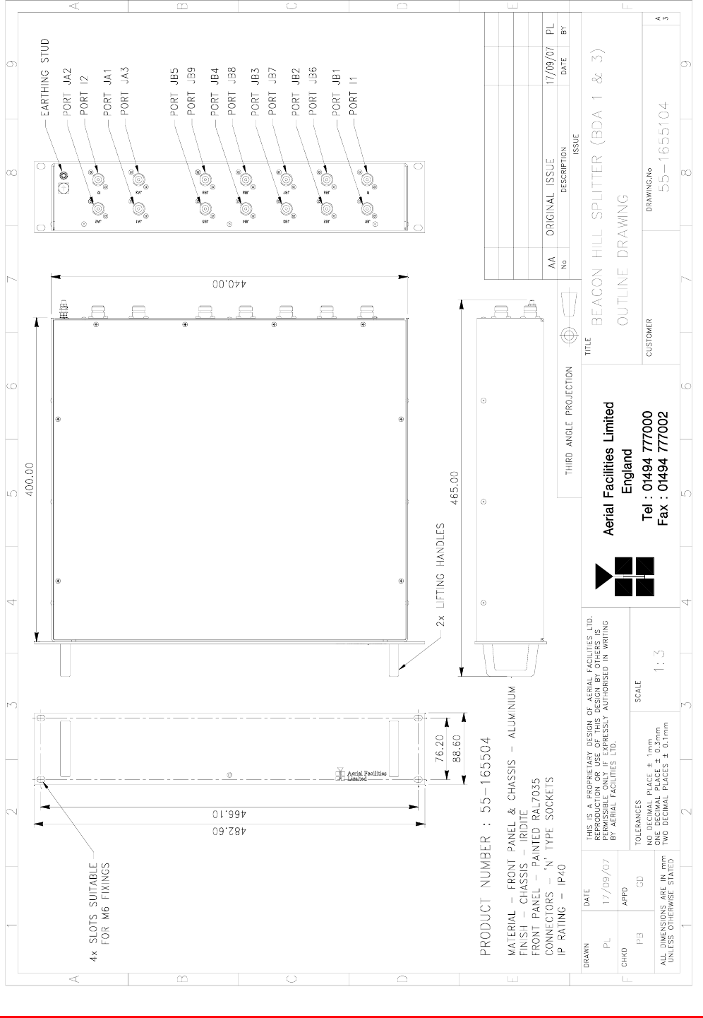
STTRS DOCUMENTATION
Document Number 80-330501HBKM – Issue A - Draft Page 78 of 500
6.3.3.1. BEACON HILL SPLITTER (BDA 1 & 3) (55-165504) Outline Drawing
Drawing number 55-1655104
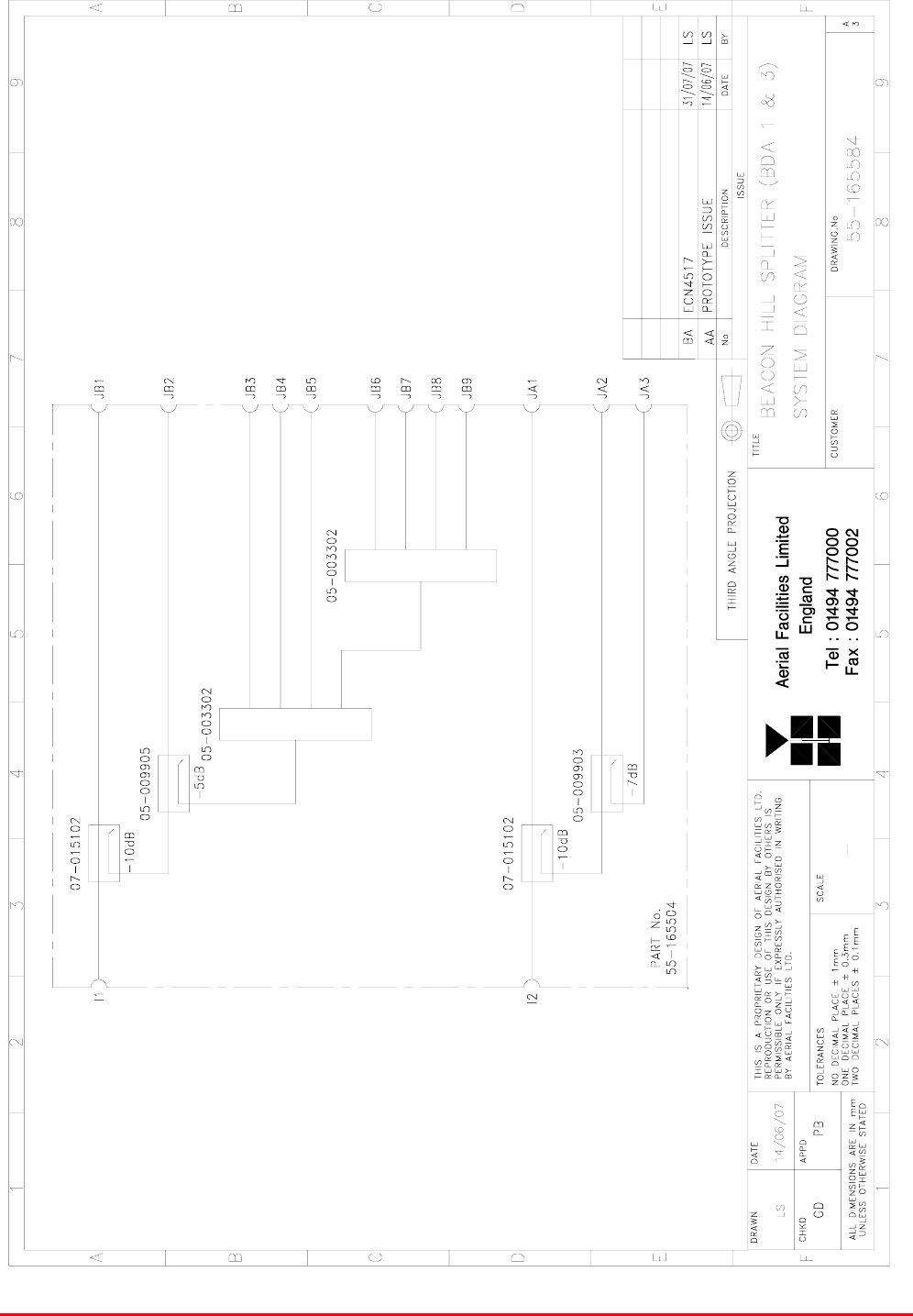
STTRS DOCUMENTATION
Document Number 80-330501HBKM – Issue A - Draft Page 79 of 500
6.3.3.2. BEACON HILL SPLITTER (BDA 1 & 3) (55-165504) System Diagram
Drawing number 55-165584

STTRS DOCUMENTATION
Document Number 80-330501HBKM – Issue A - Draft Page 80 of 500
6.3.3.3. Four Way Splitter/Combiner (05-003302)
The Splitter/Combiner used is a device for accurately matching two or more RF signals to single or
multiple ports, whilst maintaining an accurate 50Ω load to all inputs/outputs and ensuring that the
VSWR and insertion losses are kept to a minimum. Any unused ports should be terminated with an
appropriate 50 load.
Four Way Splitter (05-003302) Specification
PARAMETER SPECIFICATION
Frequency range 700-980MHz
Bandwidth 180MHz
Rejection >14dB
Insertion loss <7.0dB (in band)
Connectors N type, female
Weight <1.5kg
operational -20%C to +60%C Temperature
range: storage -40%C to +70%C
6.3.3.4. 2 Way Power Splitter/ Combiner 80/20 (05-009903)
The power Splitter/Combiner is a device for accurately matching two or more RF signals to single or
multiple ports, whilst maintaining an accurate 50Ω load to all inputs/outputs and ensuring that the
VSWR, return and insertion losses are kept to a minimum. Any unused ports will be terminated with
an appropriate 50Ω load. Power devices such as these, typically give 10dB better output isolation
than low power equivalents – (important for splitters that feed antenna systems).
05-009903 Specification
Specification Parameter
Frequency Range 764 – 860MHz
Impedence 50
Insertion Loss ± 0.3dB
VSWR 1.25:1
Splitter 100Watts Maximum
input power Combiner 5Watts
Power splitting/combining ratio 80% - 20%
RF Connectors N Female
Dimensions 104mm x 63mm x 46mm
operation: -20°C to +60°C Temperature
range storage: -40°C to +70°C
STTRS DOCUMENTATION
Document Number 80-330501HBKM – Issue A - Draft Page 81 of 500
6.3.3.5. 2 Way Power Splitter/ Combiner 70/30 (05-009905)
The power Splitter/Combiner is a device for accurately matching two or more RF signals to single or
multiple ports, whilst maintaining an accurate 50Ω load to all inputs/outputs and ensuring that the
VSWR, return and insertion losses are kept to a minimum. Any unused ports will be terminated with
an appropriate 50Ω load. Power devices such as these, typically give 10dB better output isolation
than low power equivalents – (important for splitters that feed antenna systems).
05-009905 Specification
Specification Parameter
Frequency Range 764 – 860MHz
Impedence 50
Insertion Loss ± 0.3dB
VSWR 1.25:1
Splitter 100Watts Maximum
input power Combiner 5Watts
Power splitting/combining ratio 70% - 30%
RF Connectors N Female
Dimensions 104mm x 63mm x 46mm
operation: -20°C to +60°C Temperature
range storage: -40°C to +70°C
6.3.3.6. Wideband Asymmetric Coupler (07-015102)
The purpose of Wideband Asymmetric Coupler (07-015102) is to tap off a known portion (in this case
10dB) of RF signal from transmission lines and to combine them, for example through splitter units for
different purposes (alarms/monitoring etc.), whilst maintaining an accurate 50Ω load to all
ports/interfaces throughout the specified frequency range. They are known formally as directional
couplers as they couple power from the RF mainline in one direction only.
07-015102 Specification
PARAMETER SPECIFICATION
Frequency Range 800 - 2500 MHz
Coupling Value 10 dB ± 1.0 dB
Main Line Insertion Loss <1.6 dB
VSWR 1.4:1
Directivity >18 dB
Power Rating 200 Watts
RF Connectors ‘N’ female
operation -20°C to +60°C
Temperature
range storage -40°C to +70°C

STTRS DOCUMENTATION
Document Number 80-330501HBKM – Issue A - Draft Page 82 of 500
6.3.4. Fibre Optic Splitter (55-165507)
Fibre Optic Splitter (55-165507) is a 1U rack mount tray containing an optical splitter/coupler
Fibre Optic Splitter (55-165507) List of Major Sub Components
Component
Part Component Part Description Qty. Per
Assembly
98-100001 Single Mode Optical Splitter/Coupler 1
6.4.3.1. Single Mode Optical Splitter/Coupler (98-100001)
Single Mode Optical Splitter/Couplers are used whenever it is necessary to split or combine outputs
from optical transmitters or inputs to receivers. Operators should be aware that a small insertion loss
(typically 3-4dB) is common with these type of couplers.
Single Mode Optical Splitter/Coupler (98-100001) It is an O.E.M unit featuring almost negligible
insertion loss to the F/O signal. Extreme caution should be exercised when handling these devices.
Special attention should be shown to the connectors; repair of a broken Splitter/Coupler is not
possible; replacement is the only option.
In the Fibre Optic Splitter (55-165507) in BEACON HILL STATION MASTER SITE 1 (80-330551-1),
Single Mode Optical Splitter/Coupler (98-100001) is used to split the optical signal from the FO TX
module in F/O Link Subsystem (98-700001) into two equal paths.
6.3.5. Optical AB Switch FC/APC (98-700002)
Optical A/B Switch FC/APC (98-700002) an O.E.M. sourced Fibre Optic relay supplied as a 1U rack
mount tray. 98-700002 allows for the automatic switching between two optical inputs to provide a
common optical output. Manual selection of the input is also possible via toggle switches on the front
panel.
98-700002 Specification
PARAMETER SPECIFICATION
Electrical Characteristics
Power Supply Voltage 100 - 240 VAC
Power Supply Frequency 50 - 60 Hz
Optical Characteristics
Operating Wavelength 1200 – 1610nm
Optical Input Range +20 dBm
Optical Insertion Loss 2.0 dB
Optical Trip Threshold/Meter Range -35 - +20 dBm
Optical Switch Speed 15ms
Backreflection Tolerance -50dB
Environmental and Physical Characteristics
Optical Connectors FC/APC
Operating Temp. Range +10 to +40°C
Storage Temp. Range -40 to +80 °C
Humidity 5 to 90 % RHNC
Weight 2.2 kg (6 lbs)
Dimensions 483 x 361 x 44mm (19.0 x 14.2 x 1.72 in.)

STTRS DOCUMENTATION
Document Number 80-330501HBKM – Issue A - Draft Page 83 of 500
6.3.6. F/O Link Subsystem (98-800001)
F/O Link Subsystem (98-800001) is an O.E.M. sourced Optical Tranceiver package containing
discreet TX and RX modules and supplied as a 1U rack mount tray
Parameter Specification
Optical Output Power 4 mW
Wavelength, peak 1310 1550 nm
Frequency Response, 50 to 2.2 GHz ± 1.5 dB
Input and Output VSWR 1.5:1
Link Gain (2) 0 dB
Output Noise Floor (1) -137 dBm/Hz
Input 3rd Order Intercept (1) 30 dBm
Operating Temperature 30 to +75°C
Storage Temperature 40 to +85°C
Maximum RF Input to Transmitter +20 dBm
Maximum Optical Input to Receiver 6 mW
A.C. Supply Voltage 90 – 265 VAC
Dimensions 483 x 457 x 44mm (19.0 x 18 x 1.72 in.)
(1) SFDR, Noise and IP3 specified with 5 dB optical loss.
(2) Link Gain specified with 1 meter fiber.

STTRS DOCUMENTATION
Document Number 80-330501HBKM – Issue A - Draft Page 84 of 500
7. BEACON HILL STATION MASTER SITE 2 (80-330551-2)
Cabinet number C19-CR-06
from top of rack
55-165505
55-165501
55-165501
Beacon Hill Station Master Site 2 (80-330551-2) List of major Components
section Component Part Component Part Description Qty. Per Assembly
7.3.1. 55-165501 800MHz FO HUB AMP 2
7.3.2. 55-165505 BEACON HILL SPLITTER (BDA 2 & 4) 1
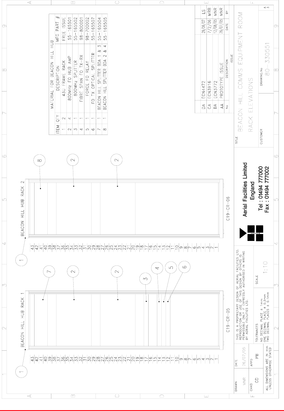
STTRS DOCUMENTATION
Document Number 80-330501HBKM – Issue A - Draft Page 85 of 500
7.1. Beacon Hill Station Master Site 2 (80-330551-2) Rack Elevation
Drawing number 80-330551
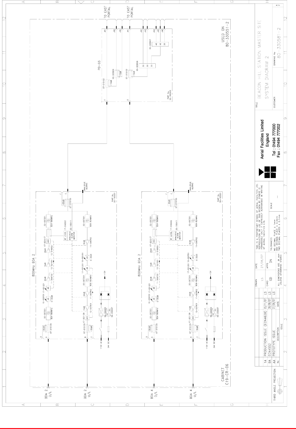
STTRS DOCUMENTATION
Document Number 80-330501HBKM – Issue A - Draft Page 86 of 500
7.2. Beacon Hill Station Master Site 2 (80-330551-2) System Diagram
Drawing number 80-330581-2
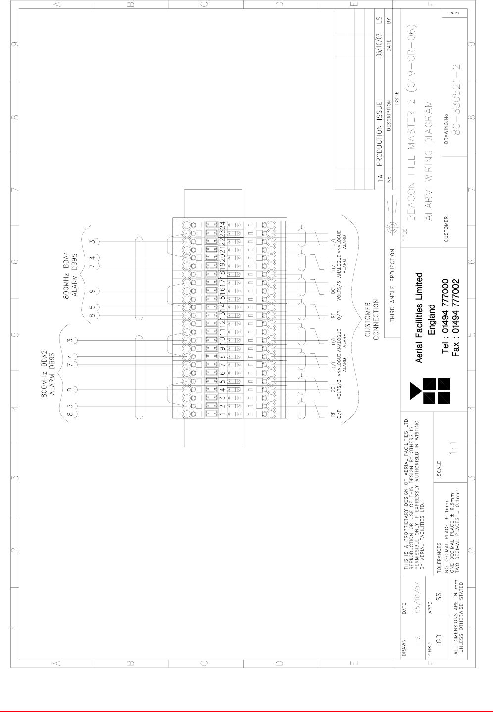
STTRS DOCUMENTATION
Document Number 80-330501HBKM – Issue A - Draft Page 87 of 500
7.3. Beacon Hill Station Master Site 2 (80-330551-2) Alarm Wiring Diagram
Drawing number 80-330521-2

STTRS DOCUMENTATION
Document Number 80-330501HBKM – Issue A - Draft Page 88 of 500
7.4. Beacon Hill Station Master Site 2 (80-330551-2) Major Sub Components
7.4.1. 800MHz FO HUB AMP (55-165501)
800MHz FO HUB AMP (55-165501) List of major components
section Component
Part Component Part Description Qty. Per
Assembly
7.4.1.3. 02-007206 Bandpass Filter 4
7.4.1.4. 07-015105 Wideband Asymmetric Coupler 3
7.4.1.5. 10-000701 Switched Attenuator 0.25Watt, 0 - 30dB 2
7.4.1.6. 11-005902 Low Noise Amplifier 1
7.4.1.7. 11-006702 Low Noise Amplifier 2
7.4.1.8. 12-018002 Power Amplifier 1
7.4.1.9. 12-021901 Low Power Amplifier 2
17-001109* AGC Detector Assembly (Logarithmic) 1
17-001117* AGC Detector Assembly 1
7.4.1.10.
17-001201* AGC Attenuator Assembly 2
7.4.1.11. 20-001601 12V (Dual) Relay Board 1
7.4.1.12. 80-008901 12V (Single) Relay Board 1
7.4.1.13. 96-200047 DC/DC Converter
7.4.1.14. 94-100004 Dual Diode Assembly 1
7.4.1.15. 96-200047 DC/DC Converter 1
7.4.1.16. 96-300052 12V Switch-Mode PSU 1
*The sub components 17-001109, 17-001117 & 17-001201 are parts of the Automatic Gain Control
(AGC) system used in 800MHz FO HUB AMP (55-165501); 17-001117 and 17-001201 are paired for
use in the uplink and 17-001109 and 17-001201 are paired for use in the downlink

STTRS DOCUMENTATION
Document Number 80-330501HBKM – Issue A - Draft Page 89 of 500
7.4.1.1. 800MHz FO HUB AMP (55-165501) Outline drawing
Drawing number 55-1655101
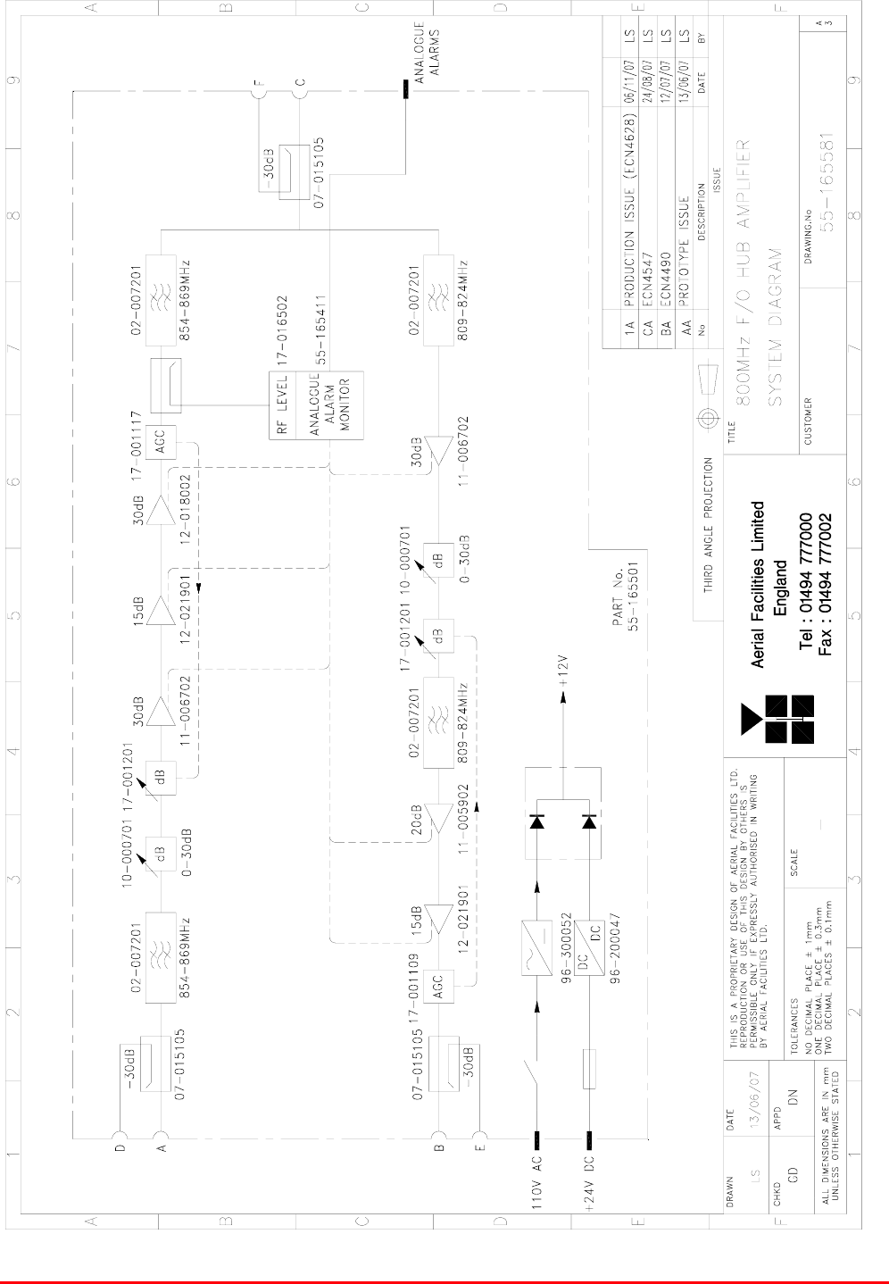
STTRS DOCUMENTATION
Document Number 80-330501HBKM – Issue A - Draft Page 90 of 500
7.4.1.2. 800MHz FO HUB AMP (55-165501) System Diagram
Drawing number 55-165581

STTRS DOCUMENTATION
Document Number 80-330501HBKM – Issue A - Draft Page 91 of 500
7.4.1.3. Bandpass Filter (02-007206)
The bandpass filters are multi-section designs with a bandwidth dependent upon the passband
frequencies, (both tuned to customer requirements). The response shape is basically Chebyshev with
a passband design ripple of 0.1dB. The filters are of slot coupled, folded combline design, and are
carefully aligned during manufacture in order to optimise the insertion loss, VSWR and
intermodulation characteristics of the unit. The tuned elements are silver-plated to reduce surface
ohmic losses and maintain a good VSWR figure and 50 load at the input and output ports.
Being passive devices, the bandpass filters should have an extremely long operational life and require
no maintenance. Should a filter be suspect, it is usually most time efficient to replace the module
rather than attempt repair or re-tuning.
No adjustments should be attempted without full network sweep analysis facilities to monitor both
insertion loss and VSWR simultaneously.
02-007206 Specification
PARAMETER SPECIFICATION
Response type Chebyshev
Frequency range 800 - 950MHz *
Bandwidth 25MHz *
Number of sections 8
Insertion loss 1.2 dB
VSWR better than 1.2:1
Connectors SMA female
Power handling 100W max
operation -20°C to +60°C Temperature
range storage -40°C to +70°C
Weight 3 kg (typical) *tuned to Customer's specification
7.4.1.4. Wideband Asymmetric Coupler (07-015105)
The purpose of Wideband Asymmetric Coupler (07-015105) is to tap off a known portion (in this case
30dB) of RF signal from transmission lines and to combine them, for example through splitter units for
different purposes (alarms/monitoring etc.), whilst maintaining an accurate 50Ω load to all
ports/interfaces throughout the specified frequency range. They are known formally as directional
couplers as they couple power from the RF mainline in one direction only.
07-015105 Specification
PARAMETER SPECIFICATION
Construction Inductive air gap
Frequency 800-2500MHz
Through loss 0.4dB (typical)
Coupling level -30dB ±0.5dB
Isolation N/A
Weight <1.0kg
Connectors SMA, female
operation -20°C to +60°C
Temperature
range storage -40°C to +70°C

STTRS DOCUMENTATION
Document Number 80-330501HBKM – Issue A - Draft Page 92 of 500
7.4.1.5. Switched Attenuator 0.25Watt, 0 - 30dB (10-000701)
In many practical applications for Cell Enhancers etc., the gain in each path is found to be excessive.
Therefore, provision is made within the unit for the setting of attenuation in each path, to reduce the
gain.
Switched Attenuator 10-000701 provides attenuation from 0 to 30dB in 2 dB steps The attenuation is
simply set using the four miniature toggle switches on the top of each unit. Each switch is clearly
marked with the attenuation it provides, and the total attenuation in line is the sum of the values
switched in. They are designed to maintain an accurate 50 impedance over their operating
frequency at both input and output.
10-000701 Specification
PARAMETER SPECIFICATION
Attenuation Values 0-30dB
Attenuation Steps 2, 4, 8 and 16dB
Power Handling 0.25 Watt
Attenuation Accuracy ± 1.0 dB
Frequency Range DC to 1GHz
Impedance 50
Connectors SMA
VSWR 1.3:1
Weight 0.2kg
operation -20°C to +60°C Temperature
range storage -40°C to +70°C

STTRS DOCUMENTATION
Document Number 80-330501HBKM – Issue A - Draft Page 93 of 500
7.4.1.6. Low Noise Amplifier (11-005902)
The Gallium-Arsenide low noise amplifier used in the unit is a double stage, solid-state low noise
amplifier. Class A circuitry is used throughout the units to ensure excellent linearity and extremely low
noise over a very wide dynamic range. The active devices are very moderately rated to provide a long
trouble-free working life. There are no adjustments on these amplifiers, and in the unlikely event of a
failure, then the complete amplifier should be replaced. This amplifier features its own in-built alarm
system which gives a volt-free relay contact type alarm that is easily integrated into any alarm system.
There is a Current Fault Alarm Function, which indicates failure of each one or both RF transistors by
a various alarm output options. The amplifier is housed in an aluminium case (Iridite NCP finish) with
SMA connectors for the RF input/output and a 9way D-type for DC and alarm outputs.
11-005902 Specification
PARAMETER SPECIFICATION
Frequency range: 800 – 960MHz *
Bandwidth: <170MHz
Gain: 19.5dB (typical)
1dB compression point: 21dBm
OIP3: 33dBm
Input/output return loss: >20dB
Noise figure: 1dB (typical)
Power consumption: 190mA @ 24V DC
Supply voltage: 10-24V DC
Connectors: SMA female
operational: -10°C to +60°C Temperature
range storage: -40°C to +70°C
Size: 90 x 55 x 30.2mm
Weight: 0.28kg *tuned to Customer's specification
LNA ‘D’ Connector Pin-out details
Connector pin Signal
1 +Ve input (10-24V)
2 GND
3 Alarm relay O/P bad
4 Alarm relay common
5 Alarm relay good
6 No connection
7 TTL voltage set
8 TTL alarm/0V (good)
9 O/C good/0V bad
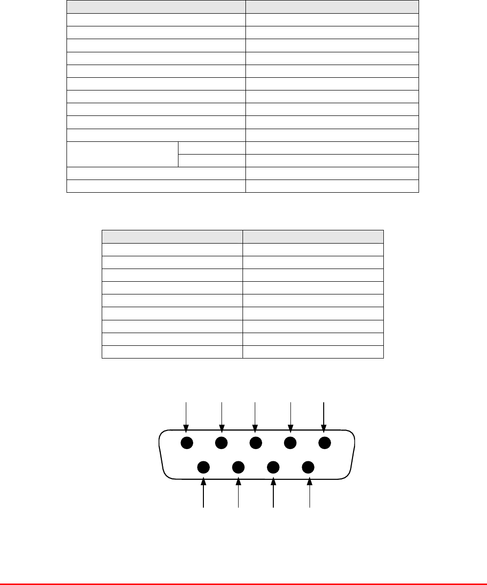
STTRS DOCUMENTATION
Document Number 80-330501HBKM – Issue A - Draft Page 94 of 500
7 8 96
1 2 3 4 5
9-Way Pin-Out Graphical Representation
7.4.1.7. Low Noise Amplifier (11-006702)
The Gallium-Arsenide low noise amplifiers used in 800MHz Line Amplifier (55-165703) are double
stage, solid-state low noise amplifiers. Class A circuitry is used throughout the units to ensure
excellent linearity and extremely low noise over a very wide dynamic range. The active devices are
very moderately rated to provide a long trouble-free working life. There are no adjustments on these
amplifiers, and in the unlikely event of a failure, then the complete amplifier should be replaced. This
amplifier features its own in-built alarm system which gives a volt-free relay contact type alarm that is
easily integrated into the main alarm system.
11-006702 Specification
PARAMETER SPECIFICATION
Frequency range: 800 – 1000MHz
Bandwidth: <200MHz
Gain: 29dB (typical)
1dB Compression point: 20dBm
OIP3: 33dBm
Input/Output return loss: >18dB
Noise figure: 1.3dB (typical)
Power consumption: 180mA @ 24V DC
Supply voltage: 10-24V DC
Connectors: SMA female
operational: -10°C to +60°C
Temperature range: storage: -20°C to +70°C
Size: 90 x 55 x 30.2mm
Weight: 290gms (approximately)
Low Noise Amplifier (11-006702) ‘D’ Connector Pin-out details
Connector pin Signal
1 +Ve input (10-24V)
2 GND
3 Alarm RelayO/P bad
4 Alarm Relay common
5 Alarm Relay good
6 No connection
7 TTL voltage set
8 TTL alarm/0V (good)
9 O/C good/0V bad
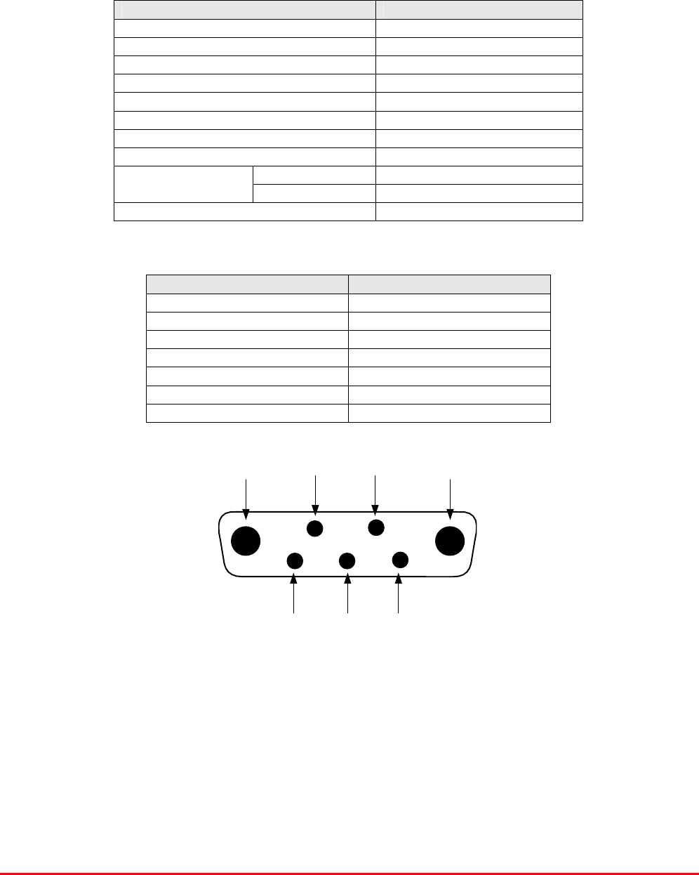
STTRS DOCUMENTATION
Document Number 80-330501HBKM – Issue A - Draft Page 95 of 500
7.4.1.8. Power Amplifier (12-018002)
This amplifier is a Class A 20W power amplifier from 800-960MHz in a 1 stage balanced
configuration. It demonstrates a very high linearity and a very good input/output return loss (RL). It
has built in a Current Fault Alarm Function.
Its housing is an aluminium case (Iridite NCP finish) with SMA connectors for the RF input/output and
a D-Type connector for the power supply and the Current Fault Alarm Function.
12-018002 Specification
PARAMETER SPECIFICATION
Frequency range: 800-960MHz
Small signal gain: 30dB
Gain flatness: ±1.2dB
I/O Return loss: >18dB
1dB compression point: 42.8dBm
OIP3: 56dBm
Supply voltage: 24V DC
Supply current: 5.0Amps (Typical)
operational: -10°C to +60°C Temperature
range storage: -20°C to +70°C
Weight: <2kg (no heatsink)
Power Amplifier (12-018002) 7-Way Connector Pin-outs
Connector Pin Signal
A1 (large pin) +24V DC
A2 (large pin) GND
1 Alarm relay common
2 TTL alarm/0V good
3 Alarm relay contact (bad)
4 Alarm relay contact (good)
5 O/C good/0V bad (TTL)

STTRS DOCUMENTATION
Document Number 80-330501HBKM – Issue A - Draft Page 96 of 500
7.4.1.9. Low Power Amplifier (12-021901)
The low power amplifier used is a triple stage solid-state low-noise amplifier. Class A circuitry is used
in the unit to ensure excellent linearity over a very wide dynamic range. The three active devices are
very moderately rated to provide a long trouble-free working life.
Its housing is an aluminium case (Iridite NCP finish) with SMA connectors for the RF input/output and
a D-Type connector for the power supply and the Current Fault Alarm Function.
There are no adjustments on this amplifier, and in the unlikely event of failure then the entire amplifier
should be replaced.
Low Power Amplifier (12-021901) Specification
PARAMETER SPECIFICATION
Frequency range 800-960MHz*
Bandwidth 20MHz *
Maximum RF output >1.0 Watt
Gain 15dB
1dB compression point +30.5dBm
3rd order intercept point +43dBm
Noise Figure <6dB
VSWR better than 1.5:1
Connectors SMA female
Supply 500mA @ 10-15V DC
operational -10°C to +60°C
Temperature
range storage -20°C to +70°C
Weight 0.5 kg
Size 167x52x25mm
* Tuned to Customer’s specification
Low Power Amplifier (12-021901) 7-Way Connector Pin-outs
Connector Pin Signal
A1 (large pin) +24V DC
A2 (large pin) GND
1 Alarm relay common
2 TTL alarm/0V good
3 Alarm relay contact (bad)
4 Alarm relay contact (good)
5 O/C good/0V bad (TTL)

STTRS DOCUMENTATION
Document Number 80-330501HBKM – Issue A - Draft Page 97 of 500
7.4.1.10. Automatic Gain Control
17-001109 AGC Detector Assembly (Logarithmic)
17-001117 AGC Detector Assembly
17-001201 AGC Attenuator Assembly
The sub components 17-001109, 17-001117 & 17-001201 are parts of the Automatic Gain Control
(AGC) system used in 800MHz FO HUB AMP (55-165501); 17-001117 and 17-001201 are paired for
use in the uplink and 17-001109 and 17-001201 are paired for use in the downlink
800MHz FO HUB AMP (55-165501) is fitted with two differing types of Automatic Gain Control (AGC)
system, one linear, and one logarithmic. The AGC with logarithmic detector (17-001117) is fitted in the
uplink path and the AGC with linear detector (17-001109) is fitted in the downlink path
The AFL Automatic Gain Control system consists of two units, a detector/amplifier and an attenuator.
The detector/amplifier unit is inserted in the RF path on the output of the power amplifier, and the
attenuator is situated in the RF path between the 1st and 2nd stages of amplification.
17-001117 and 17-001201 are paired for use in the uplink and 17-001109 and 17-001201 are paired
for use in the downlink
The attenuator comprises a 50 P.I.N diode, voltage-variable attenuator with a range of 3 to 30dB.
The attenuation is controlled by a DC voltage which is derived from the associated detector controller
board.
Normally the attenuator is at minimum attenuation. The detector/amplifier unit monitors the RF level
being delivered by the power amplifier, and when a certain threshold is reached it begins to increase
the value of the attenuator to limit the RF output to the (factory set) threshold. Therefore overloading
of the power amplifier is avoided.
The factory set threshold is 1dB below the Enhancer 1dB compression point. Some adjustment of this
AGC threshold level is possible, a 10dB range is mostly achieved. It is not recommended under any
circumstances to adjust the AGC threshold to a level greater than the 1dB compression point as
system degradation will occur.
The detector comprises of a 50 transmission line with a resistive tap which samples a small portion
of the mainline power. The sampled signal is amplified and fed to a conventional half wave diode
rectifier, the output of which is a DC voltage proportional to the RF input signal.
This DC voltage is passed via an inverting DC amplifier with integrating characteristics, to the output,
which drives the attenuation control line of the corresponding AGC attenuator. This unit is fitted at
some earlier point in the RF circuit.
For small signals, below AGC onset, the output control line will be close to 12V and the AGC
attenuator will have minimum attenuation. As the signal level increases the control line voltage will
fall, increasing the attenuator value and keeping the system output level at a constant value.

STTRS DOCUMENTATION
Document Number 80-330501HBKM – Issue A - Draft Page 98 of 500
AGC Specification (both types)
PARAMETER SPECIFICATION
Frequency range up to 1000MHz
Attenuation range 3 to 30dB
Attenuation steps continuously variable
VSWR better than 1.2:1
RF Connectors SMA female
attenuator 1W Power
handling detector/amp >30W (or as required)
operation -10°C to +60°C Temperature
range storage -20°C to +70°C
attenuator pcb 50 x 42 x 21mm
Size detector/amp pcb 54 x 42 x 21mm
attenuator 90grams
Weight detector/amp 100grams
7.4.1.11. 12V (Dual) Relay Board (20-001601)
The General Purpose Relay Board allows the inversion of signals and the isolation of circuits. It is
equipped with two dual pole change-over relays with completely isolated wiring, accessed via screw
terminals. Both relays are provided with polarity protection diodes and diodes for suppressing the
transients caused by "flywheel effect" which can destroy switching transistors or induce spikes on
neighbouring circuits. It’s common use is to amalgamate all the alarm signals into one, volts-free relay
contact pair for the main alarm system.
20-001601 Specification
PARAMETER SPECIFICATION
Operating voltage: 8 to 30V (floating earth)
Alarm threshold: Vcc - 1.20 volt +15%
Alarm output relay contacts:
Max. switch current: 1.0Amp
Max. switch volts: 120Vdc/60VA
Max. switch power: 24W/60VA
Min. switch load: 10.0µA/10.0mV
Relay isolation: 1.5kV
Mechanical life: >2x10⁷ operations
Relay approval: BT type 56
Connector details: Screw terminals
operational: -10°C to +60°C Temperature
range storage: -20°C to +70°C
STTRS DOCUMENTATION
Document Number 80-330501HBKM – Issue A - Draft Page 99 of 500
7.4.1.12. 12V (Single) Relay Board (80-008901)
The General Purpose Relay Board allows the inversion of signals and the isolation of circuits. It is
equipped with a single dual pole change-over relay RL1, with completely isolated wiring, accessed
via a 15 way in-line connector.
The relay is provided with polarity protection diodes and diodes for suppressing the transients caused
by "flywheel effect" which can destroy switching transistors or induce spikes on neighbouring circuits.
It’s common use is to amalgamate all the alarm signals into one, volts-free relay contact pair for the
main alarm system.
80-008901 Specification
PARAMETER SPECIFICATION
Operating voltage 8 to 30V (floating earth)
Alarm threshold Vcc - 1.20 volt +15%
Alarm output relay contacts:
Max. switch current 1.0Amp
Max. switch volts 120Vdc/60VA
Max. switch power 24W/60VA
Min. switch load 10.0µA/10.0mV
Relay isolation 1.5kV
Mechanical life >2x10⁷ operations
Relay approval BT type 56
Connector details Screw terminals
operational -10°C to +60°C Temperature
range storage -20°C to +70°C
7.4.1.13. DC/DC Converter 96-200047
96-200047 is an O.E.M. high power device with a wide input range and 12.5 amp @ 12V (150Watts)
output capability used to derive a 12V fixed voltage power supply rail from a higher voltage supply, in
this case 24V. In the event of failure this unit should not be repaired, only replaced.
PARAMETER SPECIFICATION
DC Input Voltage range 19 to 36V
DC Output voltage 12V ± 1%
Max. current load 12.5Amps
Operation -10°C to +60°C Temperature
range Storage -20°C to +85°C
Working Humidity 20 to 90% RHNC
7.4.1.14. Dual Diode Assembly (94-100004)
The purpose of these dual diode assemblies is to allow two DC voltage sources to be combined, so
that the main DC rail within the equipment can be sourced from either a mains driven PSU, or
externally through an XLR connector or from dual mains driven PSUs. They are very heavy-duty
diodes and they prevent any reverse current from flowing back to their source or the alternative
supply rail. Combining diodes such as these will also be used if the equipment is to be powered from
external back-up batteries.
STTRS DOCUMENTATION
Document Number 80-330501HBKM – Issue A - Draft Page 100 of 500
7.4.1.15. DC/DC Converter 96-200047
96-200047 is an O.E.M. high power device with a wide input range and 12.5 amp @ 12V (150Watts)
output capability used to derive a 12V fixed voltage power supply rail from a higher voltage supply, in
this case 12V. In the event of failure this unit should not be repaired, only replaced.
96-200047 Specification
PARAMETER SPECIFICATION
DC Input Voltage range 19 to 36V
DC Output voltage 12V ± 1%
Max. current load 12.5Amps
Operation -10°C to +60°C Temperature
range Storage -20°C to +85°C
Working Humidity 20 to 90% RHNC
7.4.1.16. 12V Switch-Mode PSU (96-300052)
No routine maintenance of the PSU is required. If a fault is suspected, then the output voltage from
the power supply may be measured on its output terminals. This is typically set to 12.2V. The
adjustment potentiometer will be found close to the DC output terminals.
All the PSUs used in AFL Cell Enhancers are capable of operation from either 110 or 220V nominal
AC supplies. The line voltage is sensed automatically, so no adjustment or link setting is needed by
the operator.
96-300052 Specification
AC Input Supply 110 or 220V nominal
Voltage 85 - 265V AC (absolute limits)
Frequency 47 to 63Hz
DC Output Supply 12V DC (nominal)
Voltage 10.5-13.8V (absolute limits)
Current 12.5A
7.4.2. BEACON HILL SPLITTER (BDA 2 & 4) (55-165505)
BEACON HILL SPLITTER (BDA 2 & 4) (55-165505) List of Major Components
Section Component
Part Component Part Description Qty. Per
Assembly
7.3.2.3. 05-009905 2 Way Power Splitter/ Combiner 70/30 1
7.3.2.4. 05-009906 3 Way Power Splitter 33/33/33 1
7.3.2.5. 05-009907 3 Way Power Splitter 40/20/40 1
7.3.2.6. 07-015102 Wideband Asymmetric Coupler 2
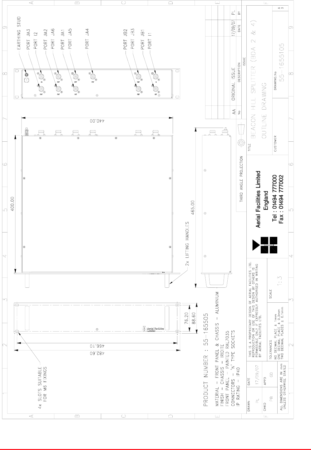
STTRS DOCUMENTATION
Document Number 80-330501HBKM – Issue A - Draft Page 101 of 500
7.4.2.1. BEACON HILL SPLITTER (BDA 2 & 4) (55-165505) Outline Drawing
Drawing Number 55-1655105
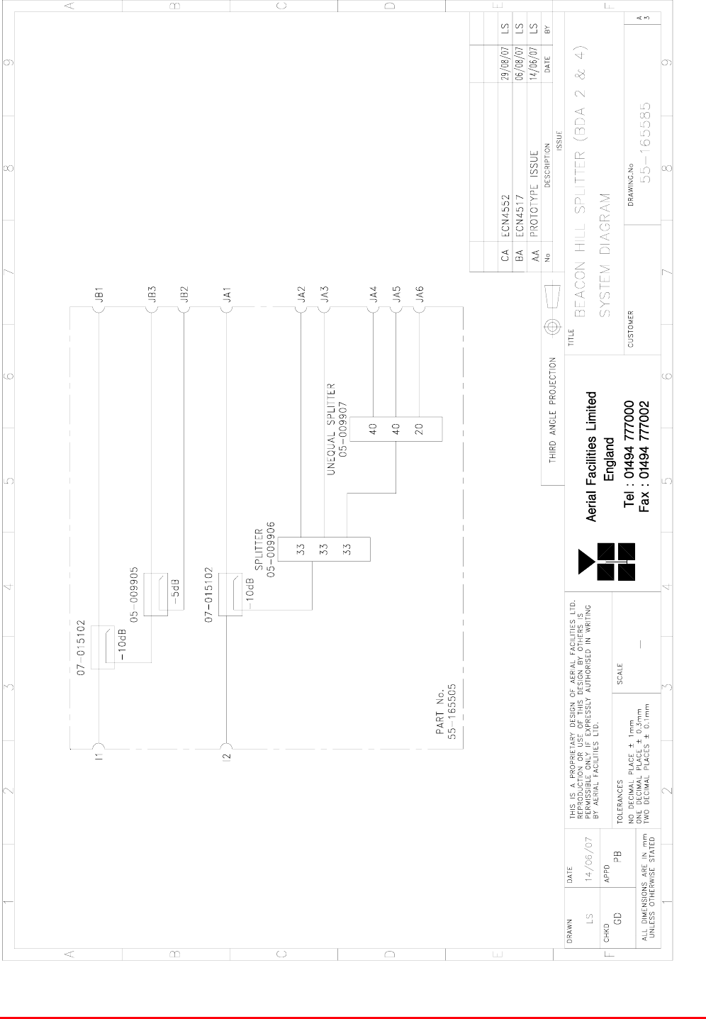
STTRS DOCUMENTATION
Document Number 80-330501HBKM – Issue A - Draft Page 102 of 500
7.4.2.2. BEACON HILL SPLITTER (BDA 2 & 4) (55-165505) System Diagram
Drawing Number 55-165585
STTRS DOCUMENTATION
Document Number 80-330501HBKM – Issue A - Draft Page 103 of 500
7.4.2.3. 2 Way Power Splitter/ Combiner 70/30 (05-009905)
The power Splitter/Combiner is a device for accurately matching two or more RF signals to single or
multiple ports, whilst maintaining an accurate 50Ω load to all inputs/outputs and ensuring that the
VSWR, return and insertion losses are kept to a minimum. Any unused ports will be terminated with
an appropriate 50Ω load. Power devices such as these, typically give 10dB better output isolation
than low power equivalents – (important for splitters that feed antenna systems).
05-009905 Specification
Specification Parameter
Frequency Range 764 – 860MHz
Impedence 50
Insertion Loss ± 0.3dB
VSWR 1.25:1
Splitter 100Watts Maximum
input power Combiner 5Watts
Power splitting/combining ratio 70% - 30%
RF Connectors N Female
Dimensions 104mm x 63mm x 46mm
operation: -20°C to +60°C Temperature
range storage: -40°C to +70°C
7.4.2.4. 3 Way Power Splitter 33/33/33 (05-009906) ***///*** BSB
7.4.2.5. 3 Way Power Splitter 40/20/40 (05-009907) ***///***BSB
7.4.2.6. Wideband Asymmetric Coupler (07-015102)
The purpose of Wideband Asymmetric Coupler (07-015102) is to tap off a known portion (in this case
10dB) of RF signal from transmission lines and to combine them, for example through splitter units for
different purposes (alarms/monitoring etc.), whilst maintaining an accurate 50Ω load to all
ports/interfaces throughout the specified frequency range. They are known formally as directional
couplers as they couple power from the RF mainline in one direction only.
07-015102 Specification
PARAMETER SPECIFICATION
Frequency Range 800 - 2500 MHz
Coupling Value 10 dB ± 1.0 dB
Main Line Insertion Loss <1.6 dB
VSWR 1.4:1
Directivity >18 dB
Power Rating 200 Watts
RF Connectors ‘N’ female
operation -20°C to +60°C
Temperature
range storage -40°C to +70°C

STTRS DOCUMENTATION
Document Number 80-330501HBKM – Issue A - Draft Page 104 of 500
8 BEACON HILL STATION CROSS PASSAGE A (80-330591-1)
Cabinet C18-CR-01
Beacon Hill Station Cross Passage A (80-330591-1) List of major Components
Component Part Component Part Description Qty. Per
Assembly
8.4.1. 07-015102 Wideband Asymmetric Coupler 1
8.4.2. 12-018002 Power Amplifier 2
8.4.3. 55-165401 800MHz Line Amplifier (Ext. Amp.) 2

STTRS DOCUMENTATION
Document Number 80-330501HBKM – Issue A - Draft Page 105 of 500
8.1. Beacon Hill Station Cross Passage A (80-330591-1) Rack Layout ***///***
Drawing number
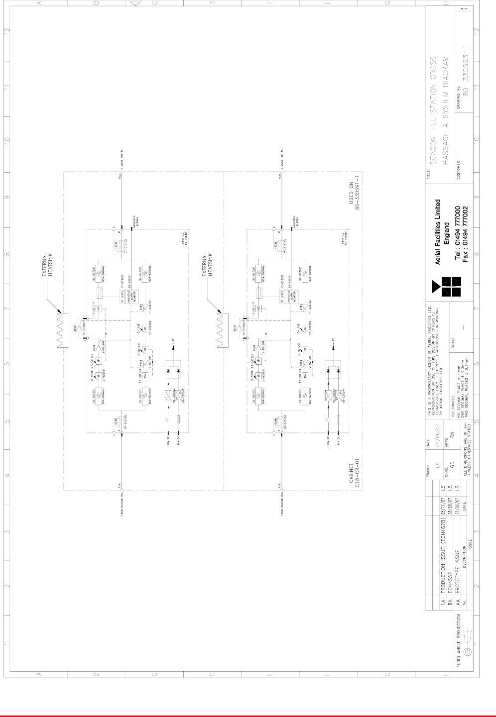
STTRS DOCUMENTATION
Document Number 80-330501HBKM – Issue A - Draft Page 106 of 500
8.2. Beacon Hill Station Cross Passage A (80-330591-1) System Diagram
Drawing number 80-330593-1
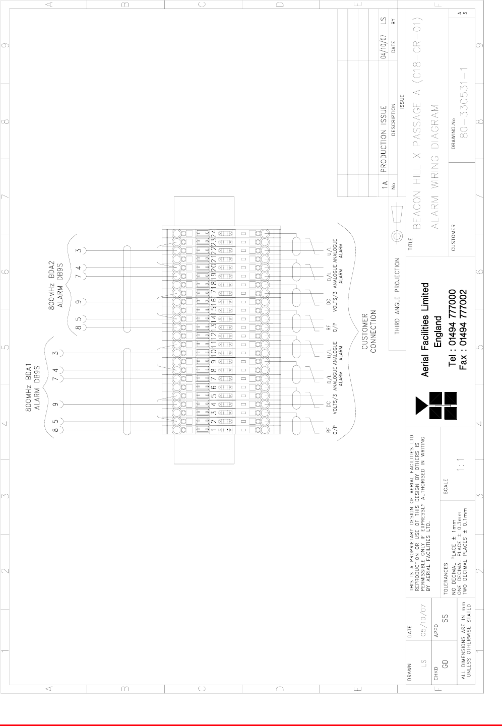
STTRS DOCUMENTATION
Document Number 80-330501HBKM – Issue A - Draft Page 107 of 500
8.3. Beacon Hill Station Cross Passage A (80-330591-1) Alarm Wiring Diagram
Drawing number 80-330531-1

STTRS DOCUMENTATION
Document Number 80-330501HBKM – Issue A - Draft Page 108 of 500
8.4. Beacon Hill Station Cross Passage A (80-330591-1) Major Sub Components
8.4.1. Wideband Asymmetric Coupler (07-015102)
The purpose of Wideband Asymmetric Coupler (07-015102) is to tap off a known portion (in this case
10dB) of RF signal from transmission lines and to combine them, for example through splitter units for
different purposes (alarms/monitoring etc.), whilst maintaining an accurate 50Ω load to all
ports/interfaces throughout the specified frequency range. They are known formally as directional
couplers as they couple power from the RF mainline in one direction only.
07-015102 Specification
PARAMETER SPECIFICATION
Frequency Range 800 - 2500 MHz
Coupling Value 10 dB ± 1.0 dB
Main Line Insertion Loss <1.6 dB
VSWR 1.4:1
Directivity >18 dB
Power Rating 200 Watts
RF Connectors ‘N’ female
operation -20°C to +60°C
Temperature
range storage -40°C to +70°C
8.4.2. Power Amplifier (12-018002)
This amplifier is a Class A 20W power amplifier from 800-960MHz in a 1 stage balanced
configuration. It demonstrates a very high linearity and a very good input/output return loss (RL). It
has built in a Current Fault Alarm Function.
Its housing is an aluminium case (Iridite NCP finish) with SMA connectors for the RF input/output and
a D-Type connector for the power supply and the Current Fault Alarm Function.
12-018002 Specification
PARAMETER SPECIFICATION
Frequency range 800-960MHz
Small signal gain 30dB
Gain flatness ±1.2dB
I/O Return loss >18dB
1dB compression point 42.8dBm
OIP3 56dBm
Supply voltage 24V DC
Supply current 5.0Amps (Typical)
operational -10°C to +60°C Temperature
range storage -20°C to +70°C
Weight <2kg (no heatsink)

STTRS DOCUMENTATION
Document Number 80-330501HBKM – Issue A - Draft Page 109 of 500
Power Amplifier (12-018002) 7-Way Connector Pin-outs
Connector Pin Signal
A1 (large pin) +24V DC
A2 (large pin) GND
1 Alarm relay common
2 TTL alarm/0V good
3 Alarm relay contact (bad)
4 Alarm relay contact (good)
5 O/C good/0V bad (TTL)

STTRS DOCUMENTATION
Document Number 80-330501HBKM – Issue A - Draft Page 110 of 500
8.4.3. 800MHz Line Amplifier (Ext. Amp.) (55-165401)
800MHz Line Amplifier (Ext. Amp.) (55-165401) list of major components
section Component
Part Component Part Description Qty. Per
Assembly
8.4.3.3. 02-007206 Bandpass Filter 4
8.4.3.4. 07-015105 Wideband Asymmetric Coupler 2
8.4.3.5. 10-000901 Switched Attenuator 0.25W, 0 - 15dB 2
8.4.3.6. 11-006702 Low Noise Amplifier 1
8.4.3.7. 12-018002K Power Amplifier 1
8.4.3.8. 12-021901 Low Power Amplifier 2
17-001109 AGC Detector Assembly (Logarithmic) 1
17-001117 AGC Detector Assembly 1
8.4.3.9.
17-001201 AGC Attenuator Assembly 2
8.4.3.10. 80-008901 12V (Single) Relay Board 1
8.4.3.11. 94-100004 Dual Diode Assembly 1
8.4.3.12. 96-200047 DC/DC Converter
8.4.3.14. 96-300052 12V Switch-Mode PSU 1
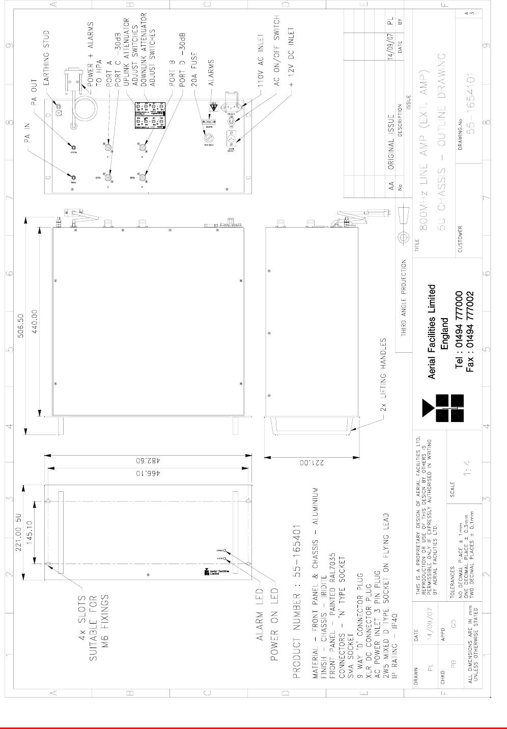
STTRS DOCUMENTATION
Document Number 80-330501HBKM – Issue A - Draft Page 111 of 500
8.4.3.1. 800MHz Line Amplifier (Ext. Amp.) (55-165401) outline drawing
Drawing number 55-1654101
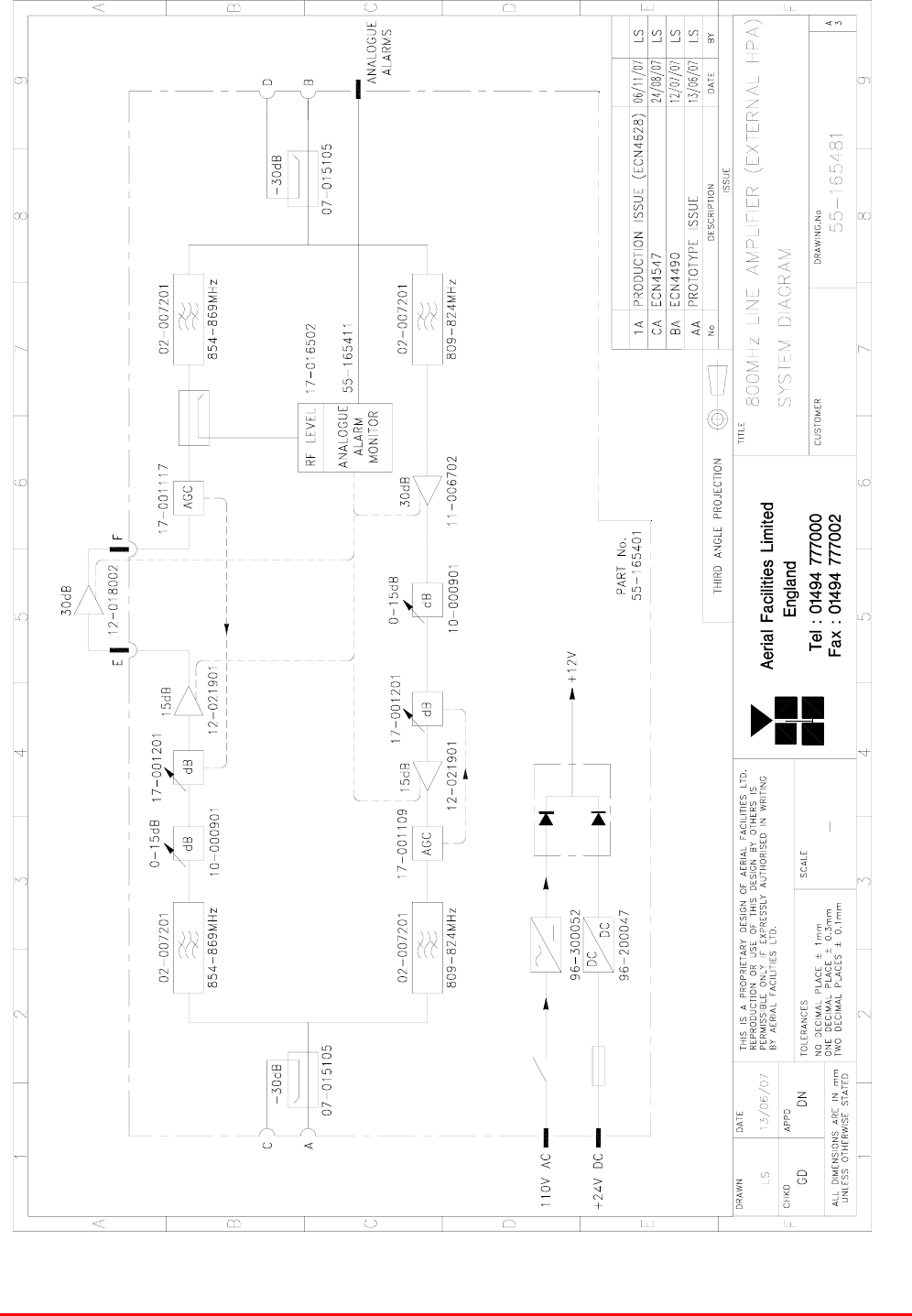
STTRS DOCUMENTATION
Document Number 80-330501HBKM – Issue A - Draft Page 112 of 500
8.4.3.2. 800MHz Line Amplifier (Ext. Amp.) (55-165401) system diagram
Drawing number 55-165481
STTRS DOCUMENTATION
Document Number 80-330501HBKM – Issue A - Draft Page 113 of 500
8.4.3.3. Bandpass Filter (02-007206)
The bandpass filters are multi-section designs with a bandwidth dependent upon the passband
frequencies, (both tuned to customer requirements). The response shape is basically Chebyshev with
a passband design ripple of 0.1dB. The filters are of slot coupled, folded combline design, and are
carefully aligned during manufacture in order to optimise the insertion loss, VSWR and
intermodulation characteristics of the unit. The tuned elements are silver-plated to reduce surface
ohmic losses and maintain a good VSWR figure and 50 load at the input and output ports.
Being passive devices, the bandpass filters should have an extremely long operational life and require
no maintenance. Should a filter be suspect, it is usually most time efficient to replace the module
rather than attempt repair or re-tuning.
No adjustments should be attempted without full network sweep analysis facilities to monitor both
insertion loss and VSWR simultaneously.
02-007206 Specification
PARAMETER SPECIFICATION
Response type Chebyshev
Frequency range 800 - 950MHz *
Bandwidth 25MHz *
Number of sections 8
Insertion loss 1.2 dB
VSWR better than 1.2:1
Connectors SMA female
Power handling 100W max
operation -20°C to +60°C Temperature
range storage -40°C to +70°C
Weight 3 kg (typical) *tuned to Customer's specification
8.4.3.4. Wideband Asymmetric Coupler (07-015105)
The purpose of Wideband Asymmetric Coupler (07-015105) is to tap off a known portion (in this case
30dB) of RF signal from transmission lines and to combine them, for example through splitter units for
different purposes (alarms/monitoring etc.), whilst maintaining an accurate 50Ω load to all
ports/interfaces throughout the specified frequency range. They are known formally as directional
couplers as they couple power from the RF mainline in one direction only.
07-015105 Specification
PARAMETER SPECIFICATION
Construction Inductive air gap
Frequency 800-2500MHz
Through loss 0.4dB (typical)
Coupling level -30dB ±0.5dB
Isolation N/A
Weight <1.0kg
Connectors SMA, female
operation -20°C to +60°C
Temperature
range storage -40°C to +70°C
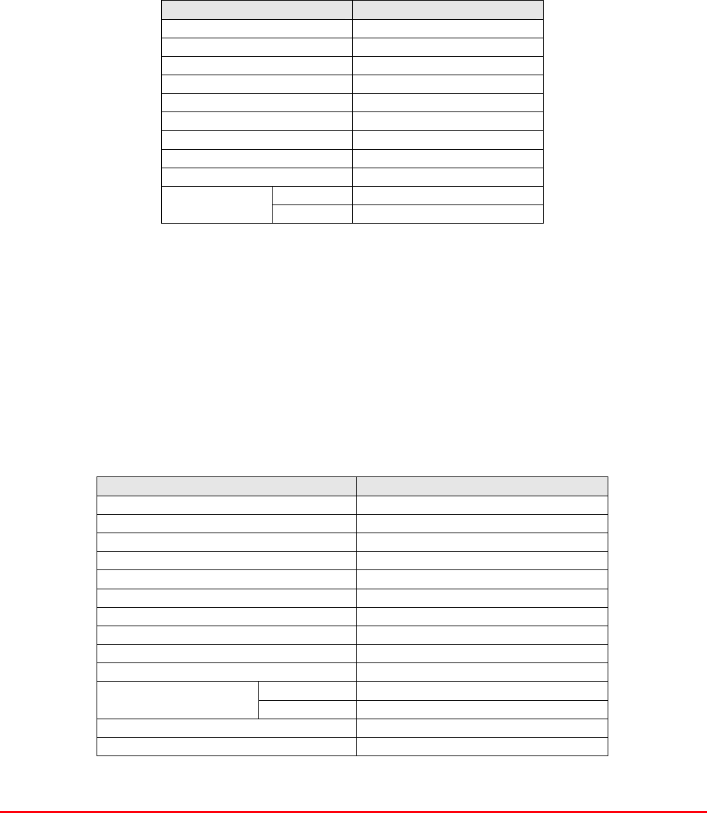
STTRS DOCUMENTATION
Document Number 80-330501HBKM – Issue A - Draft Page 114 of 500
8.4.3.5. Switched Attenuator 0.25W, 0 - 15dB (10-000901)
In many practical applications for Cell Enhancers etc., the gain in each path is found to be excessive.
Therefore, provision is made within the unit for the setting of attenuation in each path, to reduce the
gain.
10-000901 provides attenuation from 0 - 15dB in 2 dB steps The attenuation is simply set using the
four miniature toggle switches on the top of each unit. Each switch is clearly marked with the
attenuation it provides, and the total attenuation in line is the sum of the values switched in. They are
designed to maintain an accurate 50 impedance over their operating frequency at both input and
output.
10-000901 Specification
PARAMETER SPECIFICATION
Attenuation Values 0-15dB
Attenuation Steps 1, 2, 4 and 8dB
Power Handling 0.25 Watt
Attenuation Accuracy ± 1.0 dB
Frequency Range DC to 1GHz
Impedance 50
Connectors SMA
VSWR 1.3:1
Weigh 0.2kg
operation -20°C to +60°C Temperature
range storage -40°C to +70°C
8.4.3.6. Low Noise Amplifier (11-006702)
The Gallium-Arsenide low noise amplifiers used in 800MHz Line Amplifier (55-165703) are double
stage, solid-state low noise amplifiers. Class A circuitry is used throughout the units to ensure
excellent linearity and extremely low noise over a very wide dynamic range. The active devices are
very moderately rated to provide a long trouble-free working life. There are no adjustments on these
amplifiers, and in the unlikely event of a failure, then the complete amplifier should be replaced. This
amplifier features its own in-built alarm system which gives a volt-free relay contact type alarm that is
easily integrated into the main alarm system.
11-006702 Specification
PARAMETER SPECIFICATION
Frequency range: 800 – 1000MHz
Bandwidth: <200MHz
Gain: 29dB (typical)
1dB Compression point: 20dBm
OIP3: 33dBm
Input/Output return loss: >18dB
Noise figure: 1.3dB (typical)
Power consumption: 180mA @ 24V DC
Supply voltage: 10-24V DC
Connectors: SMA female
operational: -10°C to +60°C
Temperature range: storage: -20°C to +70°C
Size: 90 x 55 x 30.2mm
Weight: 290gms (approximately)
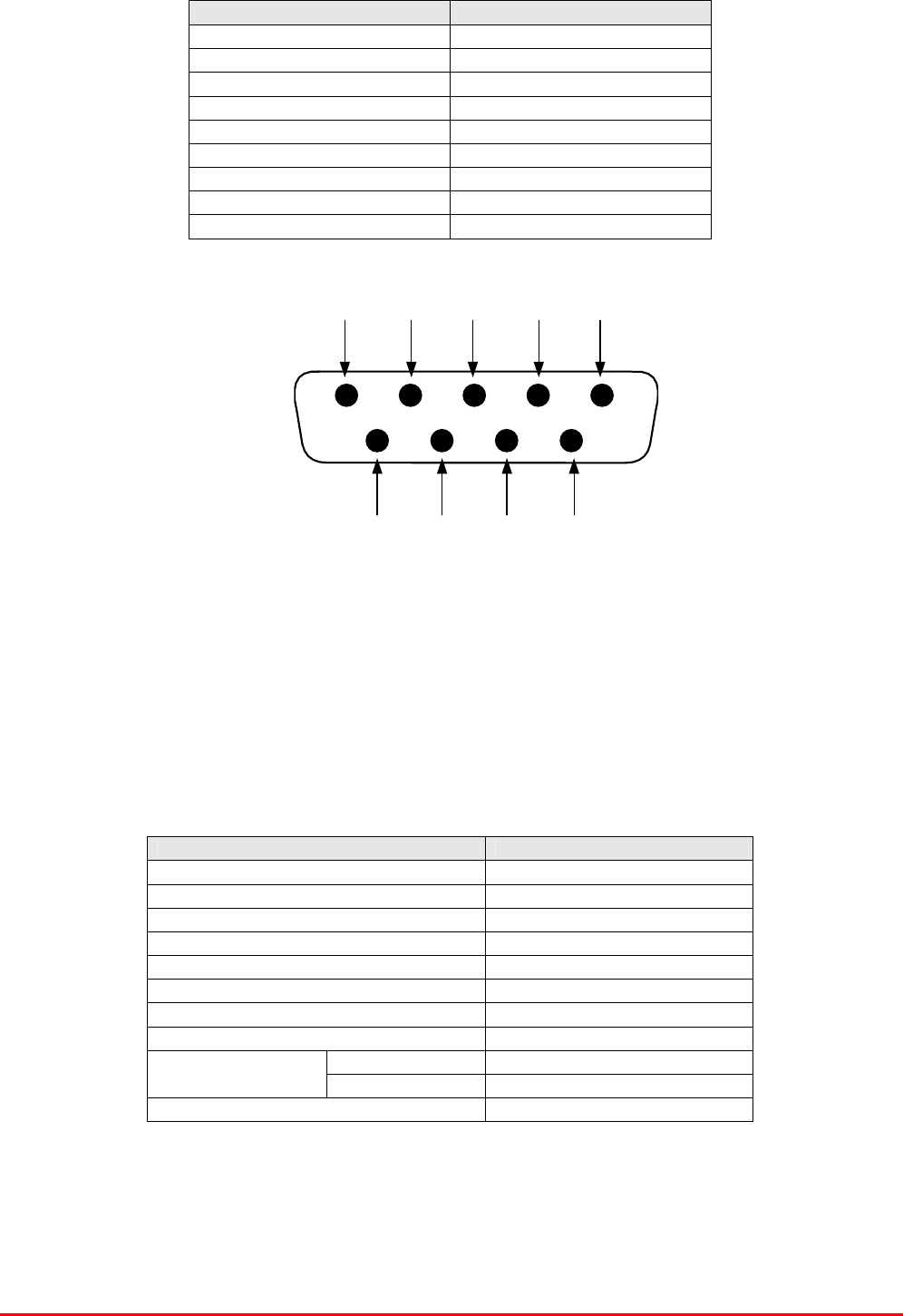
STTRS DOCUMENTATION
Document Number 80-330501HBKM – Issue A - Draft Page 115 of 500
7 8 96
1 2 3 4 5
9-Way Pin-Out Graphical Representation
Low Noise Amplifier (11-006702) ‘D’ Connector Pin-out details
Connector pin Signal
1 +Ve input (10-24V)
2 GND
3 Alarm RelayO/P bad
4 Alarm Relay common
5 Alarm Relay good
6 No connection
7 TTL voltage set
8 TTL alarm/0V (good)
9 O/C good/0V bad
8.4.3.7. Power Amplifier (12-018002)
This amplifier is a Class A 20W power amplifier from 800-960MHz in a 1 stage balanced
configuration. It demonstrates a very high linearity and a very good input/output return loss (RL). It
has built in a Current Fault Alarm Function.
Its housing is an aluminium case (Iridite NCP finish) with SMA connectors for the RF input/output and
a D-Type connector for the power supply and the Current Fault Alarm Function.
12-018002 Specification
PARAMETER SPECIFICATION
Frequency range: 800-960MHz
Small signal gain: 30dB
Gain flatness: ±1.2dB
I/O Return loss: >18dB
1dB compression point: 42.8dBm
OIP3: 56dBm
Supply voltage: 24V DC
Supply current: 5.0Amps (Typical)
operational: -10°C to +60°C Temperature
range storage: -20°C to +70°C
Weight: <2kg (no heatsink)
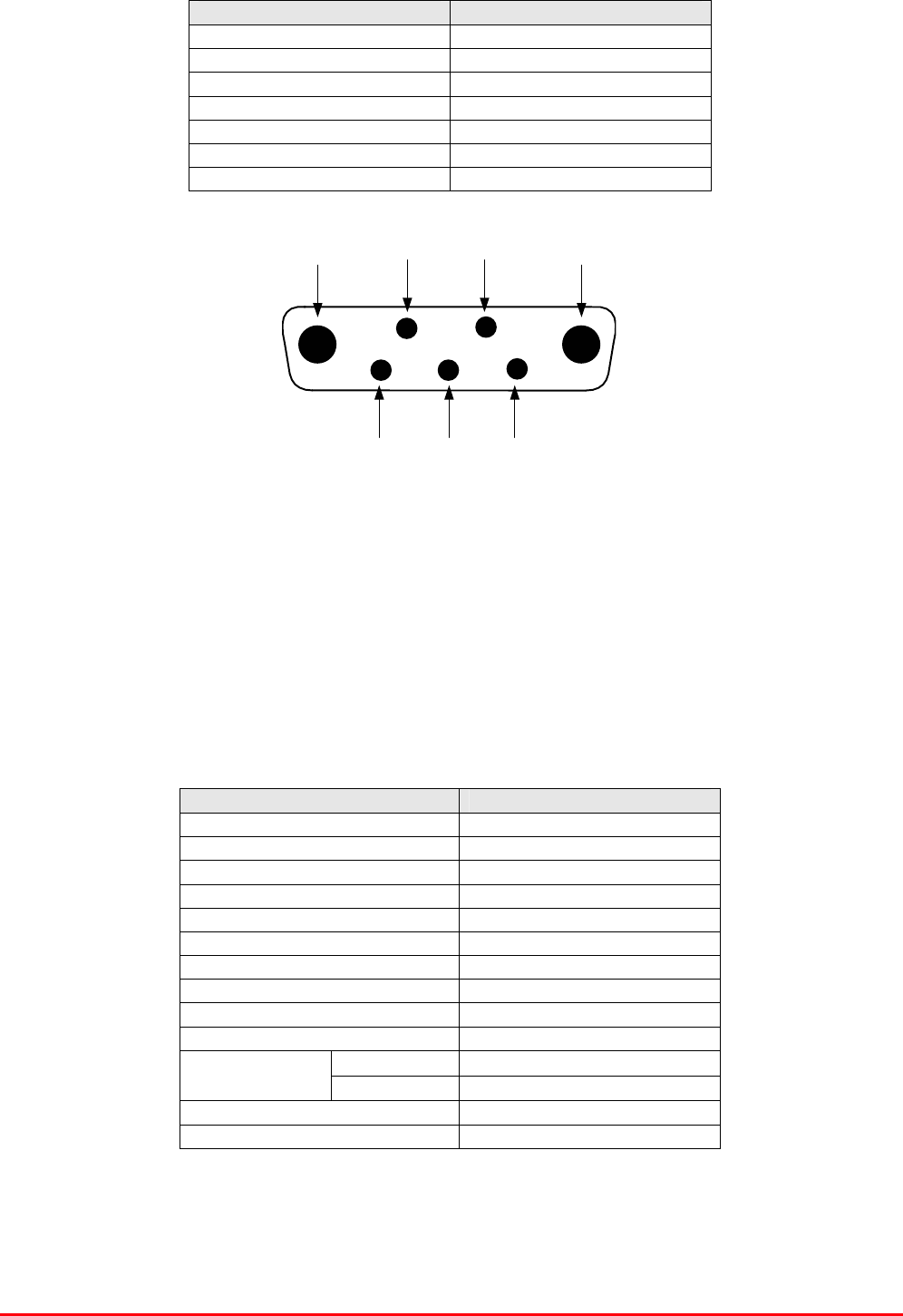
STTRS DOCUMENTATION
Document Number 80-330501HBKM – Issue A - Draft Page 116 of 500
Power Amplifier (12-018002) 7-Way Connector Pin-outs
Connector Pin Signal
A1 (large pin) +24V DC
A2 (large pin) GND
1 Alarm relay common
2 TTL alarm/0V good
3 Alarm relay contact (bad)
4 Alarm relay contact (good)
5 O/C good/0V bad (TTL)
8.4.3.8. Low Power Amplifier (12-021901)
The low power amplifier used is a triple stage solid-state low-noise amplifier. Class A circuitry is used
in the unit to ensure excellent linearity over a very wide dynamic range. The three active devices are
very moderately rated to provide a long trouble-free working life.
Its housing is an aluminium case (Iridite NCP finish) with SMA connectors for the RF input/output and
a D-Type connector for the power supply and the Current Fault Alarm Function.
There are no adjustments on this amplifier, and in the unlikely event of failure then the entire amplifier
should be replaced.
Low Power Amplifier (12-021901) Specification
PARAMETER SPECIFICATION
Frequency range 800-960MHz*
Bandwidth 20MHz *
Maximum RF output >1.0 Watt
Gain 15dB
1dB compression point +30.5dBm
3rd order intercept point +43dBm
Noise Figure <6dB
VSWR better than 1.5:1
Connectors SMA female
Supply 500mA @ 10-15V DC
operational -10°C to +60°C
Temperature
range storage -20°C to +70°C
Weight 0.5 kg
Size 167x52x25mm
* Tuned to Customer’s specification

STTRS DOCUMENTATION
Document Number 80-330501HBKM – Issue A - Draft Page 117 of 500
Low Power Amplifier (12-021901) 7-Way Connector Pin-outs
Connector Pin Signal
A1 (large pin) +24V DC
A2 (large pin) GND
1 Alarm relay common
2 TTL alarm/0V good
3 Alarm relay contact (bad)
4 Alarm relay contact (good)
5 O/C good/0V bad (TTL)
8.4.3.9. Automatic Gain Control
17-001109 AGC Detector Assembly (Logarithmic)
17-001117 AGC Detector Assembly
17-001201 AGC Attenuator Assembly
The sub components 17-001109, 17-001117 & 17-001201 are parts of the Automatic Gain Control
(AGC) system used in 800MHz Line Amplifier (Ext. Amp.) (55-165401); 17-001117 and 17-001201
are paired for use in the uplink and 17-001109 and 17-001201 are paired for use in the downlink
800MHz Line Amplifier (Ext. Amp.) (55-165401) is fitted with two differing types of Automatic Gain
Control (AGC) system, one linear, and one logarithmic. The AGC with logarithmic detector (17-
001117) is fitted in the uplink path and the AGC with linear detector (17-001109) is fitted in the
downlink path
The AFL Automatic Gain Control system consists of two units, a detector/amplifier and an attenuator.
The detector/amplifier unit is inserted in the RF path on the output of the power amplifier, and the
attenuator is situated in the RF path between the 1st and 2nd stages of amplification.
17-001117 and 17-001201 are paired for use in the uplink and 17-001109 and 17-001201 are paired
for use in the downlink
The attenuator comprises a 50 P.I.N diode, voltage-variable attenuator with a range of 3 to 30dB.
The attenuation is controlled by a DC voltage which is derived from the associated detector controller
board.
Normally the attenuator is at minimum attenuation. The detector/amplifier unit monitors the RF level
being delivered by the power amplifier, and when a certain threshold is reached it begins to increase
the value of the attenuator to limit the RF output to the (factory set) threshold. Therefore overloading
of the power amplifier is avoided.
The factory set threshold is 1dB below the Enhancer 1dB compression point. Some adjustment of this
AGC threshold level is possible, a 10dB range is mostly achieved. It is not recommended under any
circumstances to adjust the AGC threshold to a level greater than the 1dB compression point as
system degradation will occur.
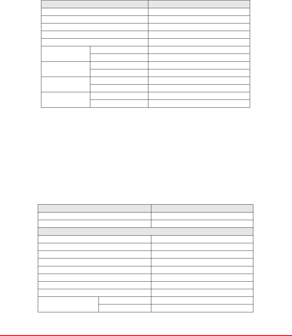
STTRS DOCUMENTATION
Document Number 80-330501HBKM – Issue A - Draft Page 118 of 500
The detector comprises of a 50 transmission line with a resistive tap which samples a small portion
of the mainline power. The sampled signal is amplified and fed to a conventional half wave diode
rectifier, the output of which is a DC voltage proportional to the RF input signal.
This DC voltage is passed via an inverting DC amplifier with integrating characteristics, to the output,
which drives the attenuation control line of the corresponding AGC attenuator. This unit is fitted at
some earlier point in the RF circuit.
For small signals, below AGC onset, the output control line will be close to 12V and the AGC
attenuator will have minimum attenuation. As the signal level increases the control line voltage will
fall, increasing the attenuator value and keeping the system output level at a constant value.
AGC Specification (both types)
PARAMETER SPECIFICATION
Frequency range up to 1000MHz
Attenuation range 3 to 30dB
Attenuation steps continuously variable
VSWR better than 1.2:1
RF Connectors SMA female
attenuator 1W Power
handling detector/amp >30W (or as required)
operation -10°C to +60°C Temperature
range storage -20°C to +70°C
attenuator pcb 50 x 42 x 21mm
Size detector/amp pcb 54 x 42 x 21mm
attenuator 90grams
Weight detector/amp 100grams
8.4.3.10. 12V (Single) Relay Board (80-008901)
The General Purpose Relay Board allows the inversion of signals and the isolation of circuits. It is
equipped with a single dual pole change-over relay RL1, with completely isolated wiring, accessed
via a 15 way in-line connector. The relay is provided with polarity protection diodes and diodes for
suppressing the transients caused by "flywheel effect" which can destroy switching transistors or
induce spikes on neighbouring circuits. It’s common use is to amalgamate all the alarm signals into
one, volts-free relay contact pair for the main alarm system.
80-008901 Specification
PARAMETER SPECIFICATION
Operating voltage 8 to 30V (floating earth)
Alarm threshold Vcc - 1.20 volt +15%
Alarm output relay contacts:
Max. switch current 1.0Amp
Max. switch volts 120Vdc/60VA
Max. switch power 24W/60VA
Min. switch load 10.0µA/10.0mV
Relay isolation 1.5kV
Mechanical life >2x10⁷ operations
Relay approval BT type 56
Connector details Screw terminals
operationa: -10°C to +60°C Temperature
range storage -20°C to +70°C
STTRS DOCUMENTATION
Document Number 80-330501HBKM – Issue A - Draft Page 119 of 500
8.4.3.11. Dual Diode Assembly (94-100004)
The purpose of these dual diode assemblies is to allow two DC voltage sources to be combined, so
that the main DC rail within the equipment can be sourced from either a mains driven PSU, or
externally through an XLR connector or from dual mains driven PSUs . They are very heavy-duty
diodes and they prevent any reverse current from flowing back to their source or the alternative
supply rail. Combining diodes such as these will also be used if the equipment is to be powered from
external back-up batteries.
8.4.3.12. DC/DC Converter (96-200047)
DC/DC Converter 96-200047
96-200047 is an O.E.M. high power device with a wide input range and 12.5 amp @ 12V (150Watts)
output capability used to derive a 12V fixed voltage power supply rail from a higher voltage supply, in
this case 24V. In the event of failure this unit should not be repaired, only replaced.
PARAMETER SPECIFICATION
DC Input Voltage range 19 to 36V
DC Output voltage 12V ± 1%
Max. current load 12.5Amps
Operation -10°C to +60°C Temperature
range Storage -20°C to +85°C
Working Humidity 20 to 90% RHNC
8.4.3.13. 12V Switch-Mode PSU (96-300052)
No routine maintenance of the PSU is required. If a fault is suspected, then the output voltage from
the power supply may be measured on its output terminals. This is typically set to 12.2V. The
adjustment potentiometer will be found close to the DC output terminals.
All the PSUs used in AFL Cell Enhancers are capable of operation from either 110 or 220V nominal
AC supplies. The line voltage is sensed automatically, so no adjustment or link setting is needed by
the operator.
96-300052 Specification
AC Input Supply 110 or 220V nominal
Voltage 85 - 265V AC
(absolute limits)
Frequency 47 to 63Hz
DC Output Supply 12V DC (nominal)
Voltage 10.5-13.8V (absolute limits)
Current 12.5A

STTRS DOCUMENTATION
Document Number 80-330501HBKM – Issue A - Draft Page 120 of 500
9 BEACON HILL STATION CROSS PASSAGE B (80-330591-2)
Cabinet C20-CR-01
Beacon Hill Station Cross Passage B (80-330591-2) List of major Components
Component Part Component Part Description Qty. Per
Assembly
9.4.1. 07-015102 Wideband Asymmetric Coupler 1
9.4.2. 12-018002 Power Amplifier 2
9.4.3. 55-165401 800MHz Line Amplifier (Ext. Amp.) 2

STTRS DOCUMENTATION
Document Number 80-330501HBKM – Issue A - Draft Page 121 of 500
9.1. Beacon Hill Station Cross Passage B (80-330591-2) Rack layout ***///***
Drawing number
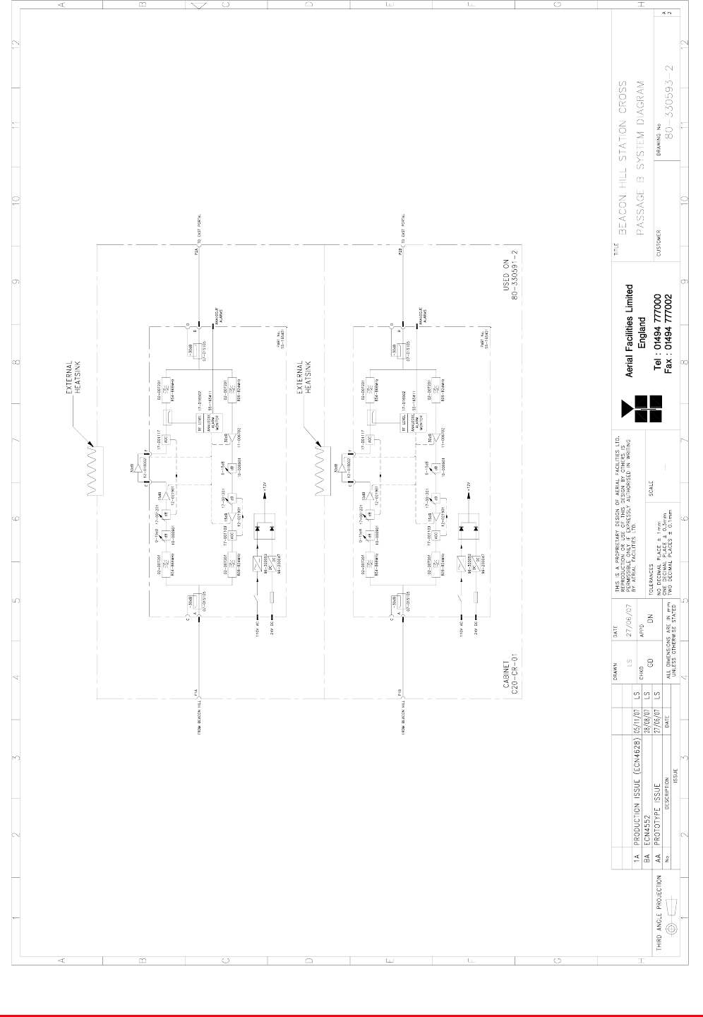
STTRS DOCUMENTATION
Document Number 80-330501HBKM – Issue A - Draft Page 122 of 500
9.2. Beacon Hill Station Cross Passage B (80-330591-2) System Diagram
Drawing number 80-330593-2
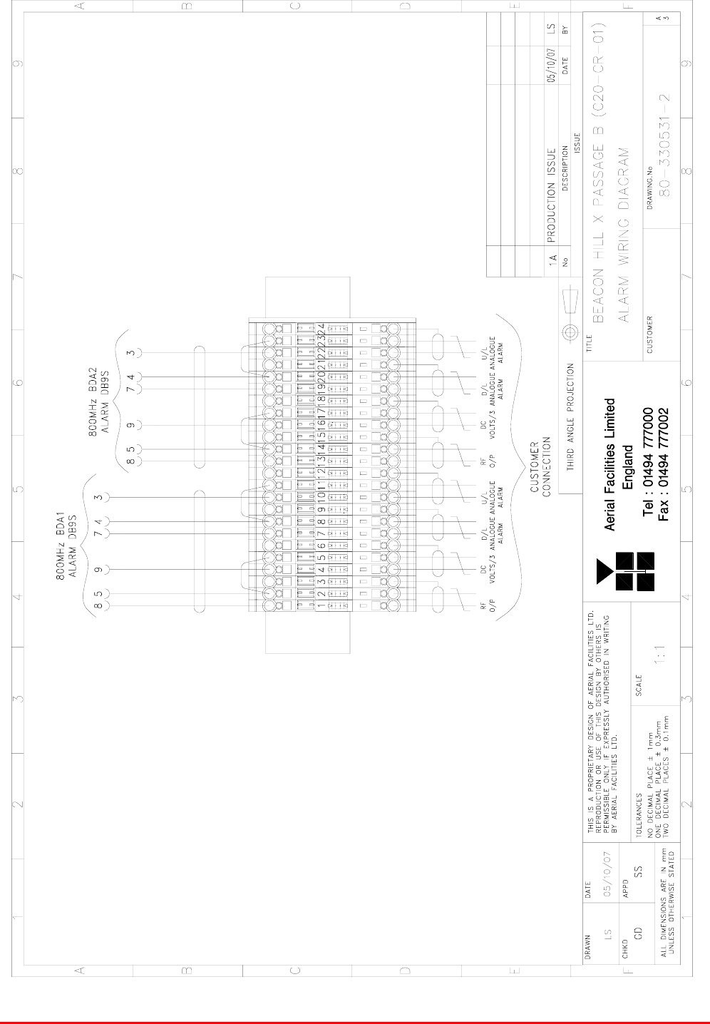
STTRS DOCUMENTATION
Document Number 80-330501HBKM – Issue A - Draft Page 123 of 500
9.3. Beacon Hill Station Cross Passage B (80-330591-2) Alarm Wiring Diagram
Drawing number 80-330531-2
STTRS DOCUMENTATION
Document Number 80-330501HBKM – Issue A - Draft Page 124 of 500
9.4. Beacon Hill Station Cross Passage A (80-330591-1) Major Sub Components
9.4.1. Wideband Asymmetric Coupler (07-015102)
The purpose of Wideband Asymmetric Coupler (07-015102) is to tap off a known portion (in this case
10dB) of RF signal from transmission lines and to combine them, for example through splitter units for
different purposes (alarms/monitoring etc.), whilst maintaining an accurate 50Ω load to all
ports/interfaces throughout the specified frequency range. They are known formally as directional
couplers as they couple power from the RF mainline in one direction only.
07-015102 Specification
PARAMETER SPECIFICATION
Frequency Range 800 - 2500 MHz
Coupling Value 10 dB ± 1.0 dB
Main Line Insertion Loss <1.6 dB
VSWR 1.4:1
Directivity >18 dB
Power Rating 200 Watts
RF Connectors ‘N’ female
operation -20°C to +60°C
Temperature
range storage -40°C to +70°C
9.4.2. Power Amplifier (12-018002)
This amplifier is a Class A 20W power amplifier from 800-960MHz in a 1 stage balanced
configuration. It demonstrates a very high linearity and a very good input/output return loss (RL). It
has built in a Current Fault Alarm Function.
Its housing is an aluminium case (Iridite NCP finish) with SMA connectors for the RF input/output and
a D-Type connector for the power supply and the Current Fault Alarm Function.
12-018002 Specification
PARAMETER SPECIFICATION
Frequency range: 800-960MHz
Small signal gain: 30dB
Gain flatness: ±1.2dB
I/O Return loss: >18dB
1dB compression point: 42.8dBm
OIP3: 56dBm
Supply voltage: 24V DC
Supply current: 5.0Amps (Typical)
operational: -10°C to +60°C Temperature
range storage: -20°C to +70°C
Weight: <2kg (no heatsink)

STTRS DOCUMENTATION
Document Number 80-330501HBKM – Issue A - Draft Page 125 of 500
Power Amplifier (12-018002) 7-Way Connector Pin-outs
Connector Pin Signal
A1 (large pin) +24V DC
A2 (large pin) GND
1 Alarm relay common
2 TTL alarm/0V good
3 Alarm relay contact (bad)
4 Alarm relay contact (good)
5 O/C good/0V bad (TTL)