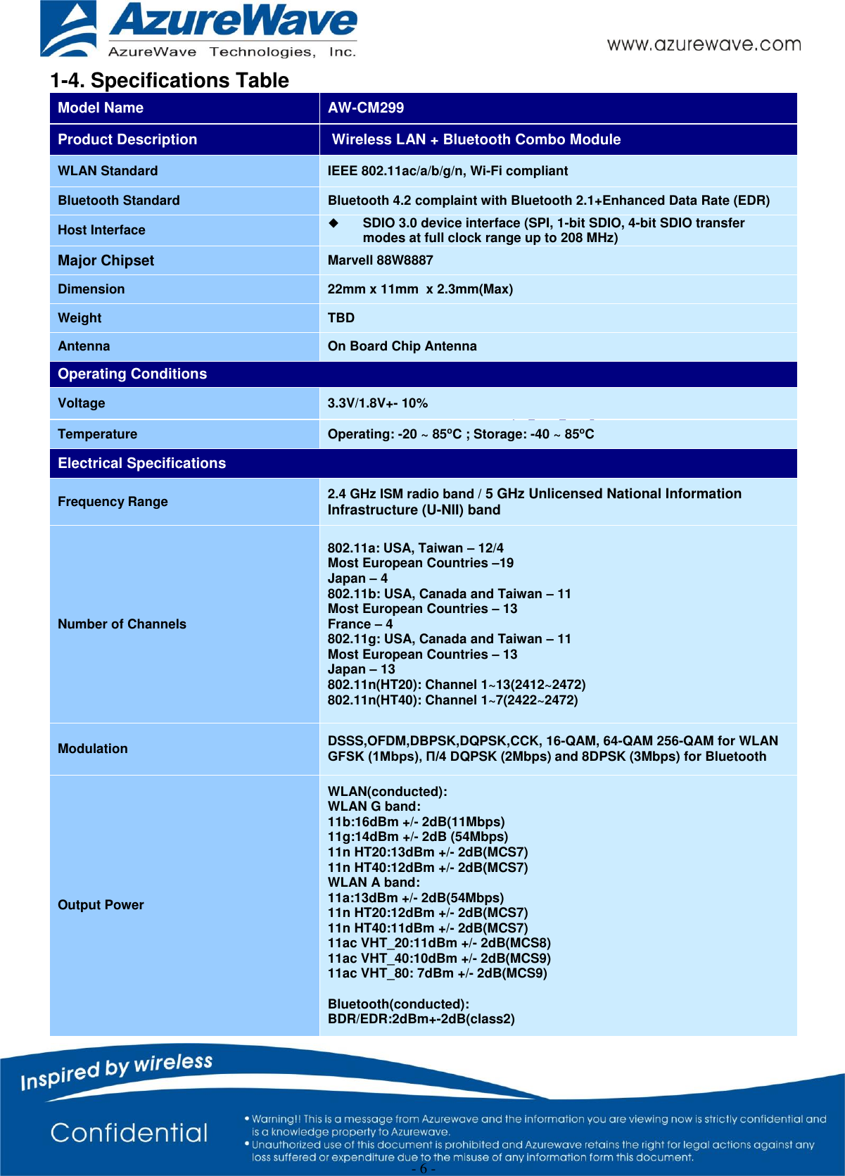
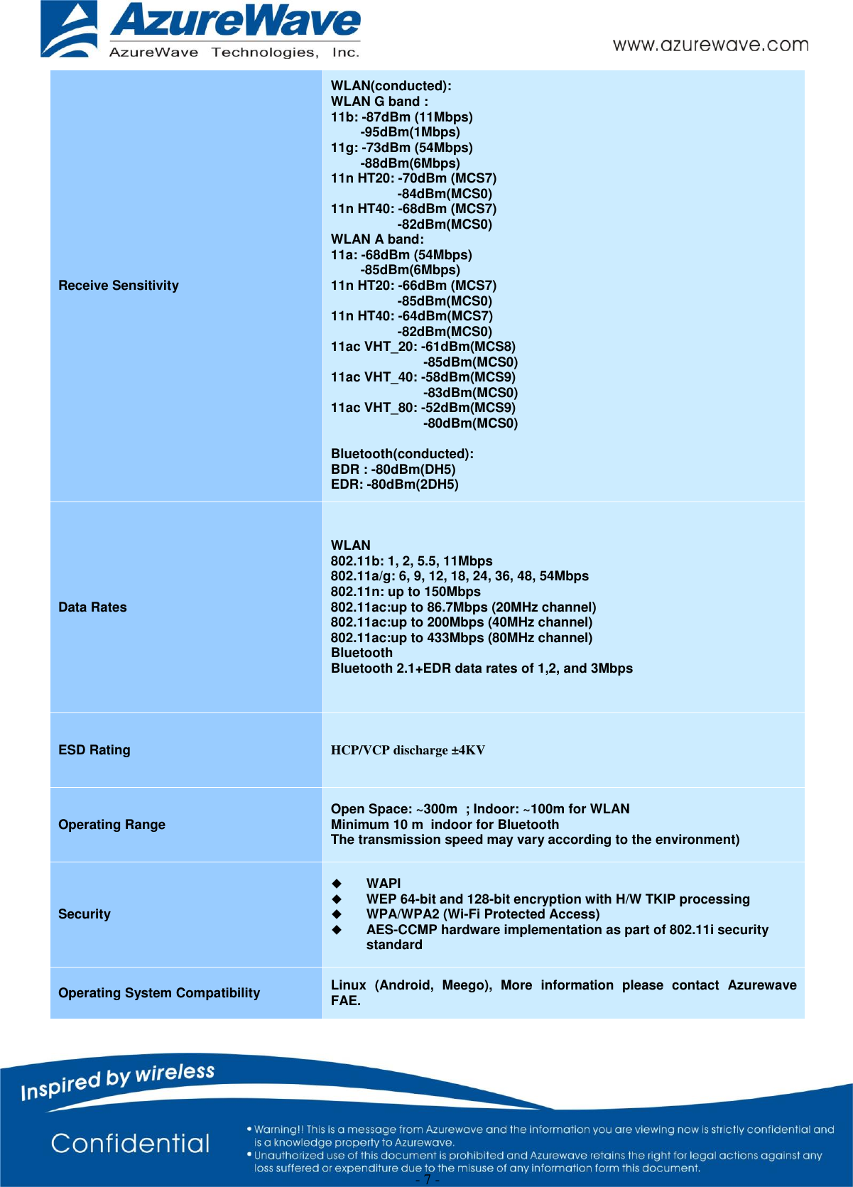
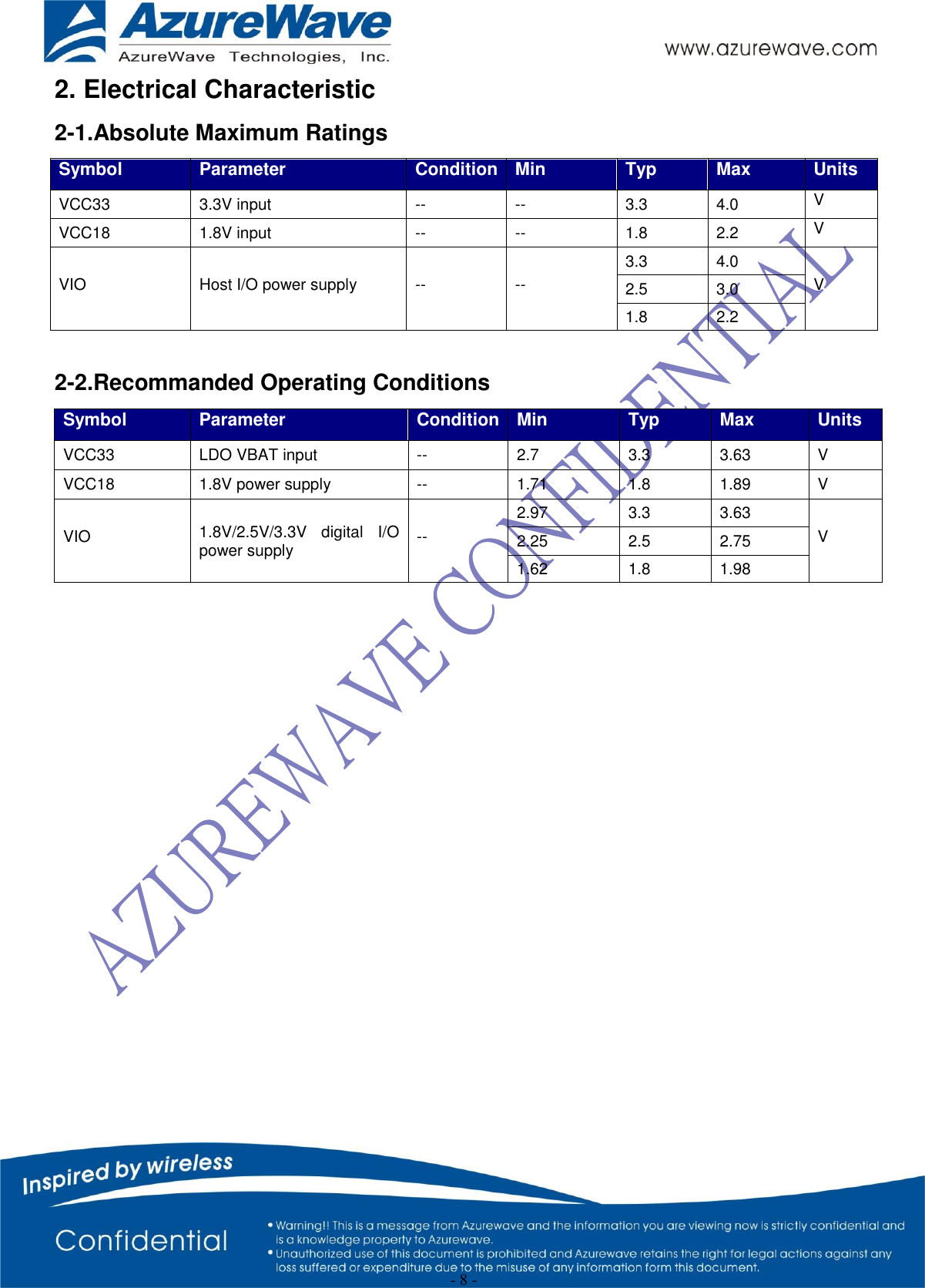
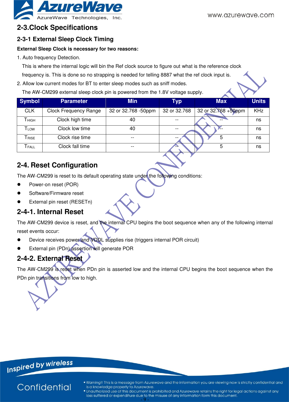
AzureWave Technologies CM299 IEEE 802.11 1X1 ac/a/b/g/n Wireless LAN + Bluetooth Module User Manual AW CH387
AzureWave Technologies, Inc. IEEE 802.11 1X1 ac/a/b/g/n Wireless LAN + Bluetooth Module AW CH387
UserManual.wiki
>
AzureWave Technologies
>
CM299 User Manual
Users Manual
Navigation menu
Upload a User Manual
Namespaces
Wiki Guide
HTML
PDF
Info
Views
User Manual
Discussion / Help
Navigation
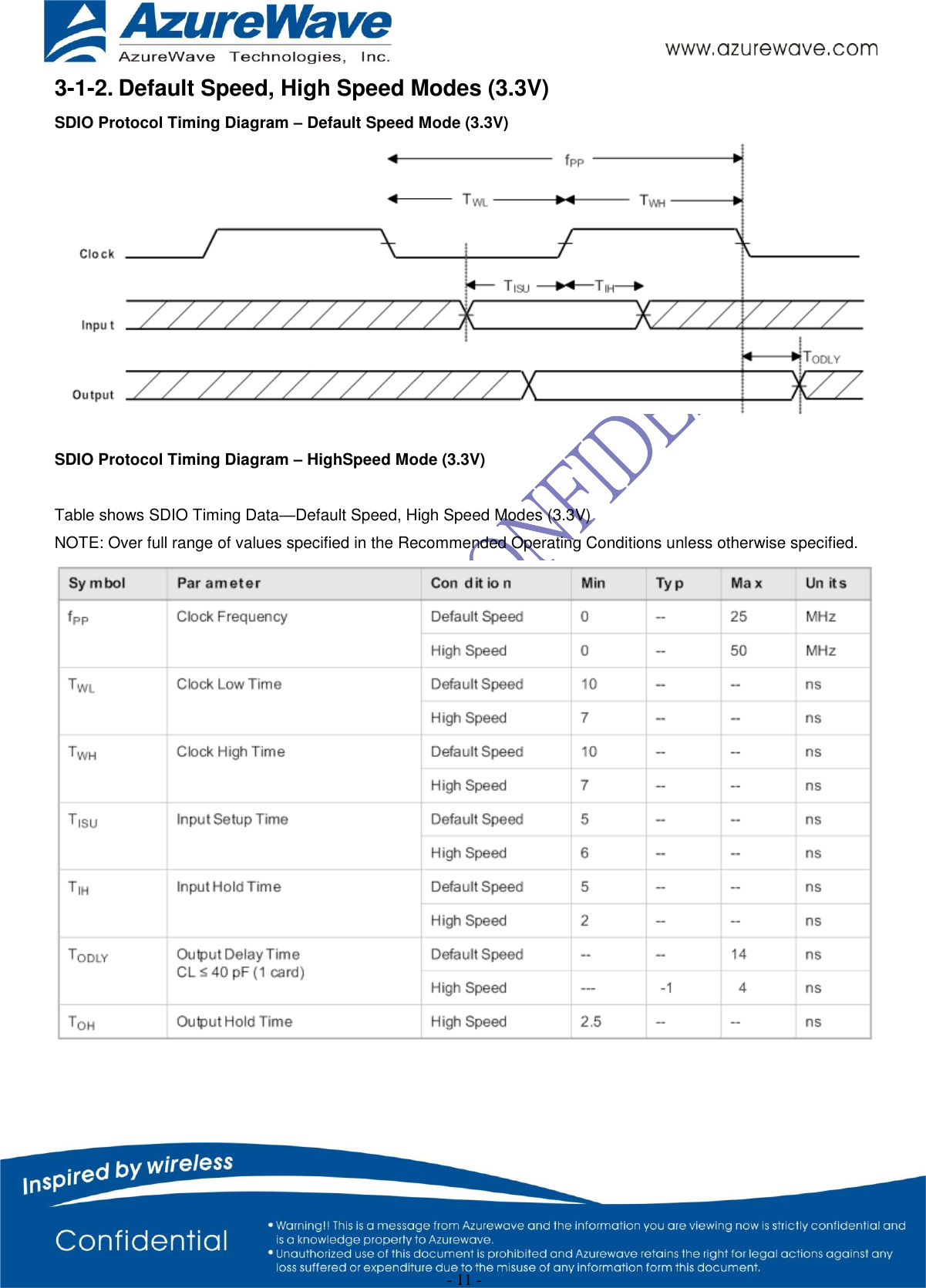
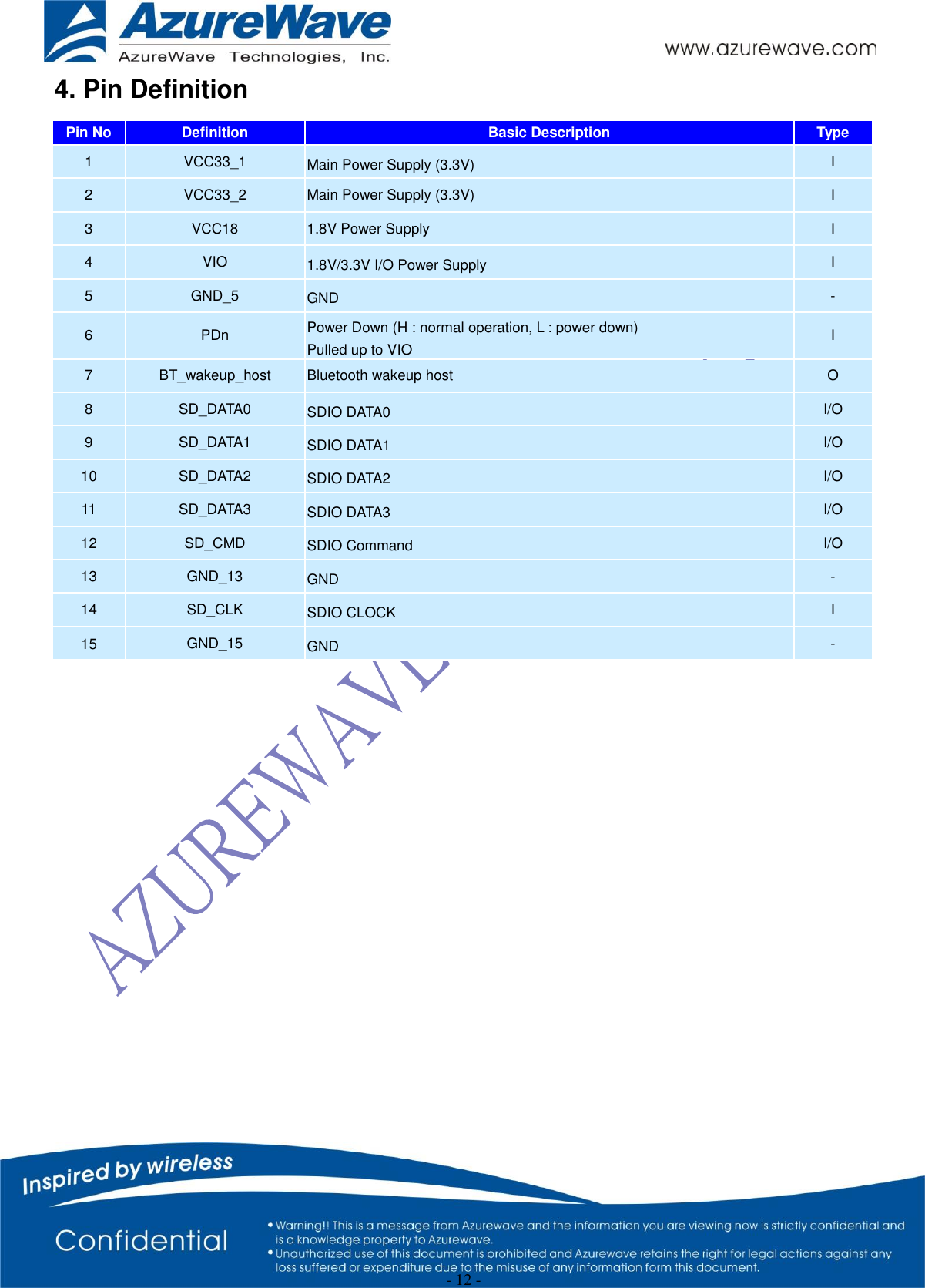
![- 10 - 3. Host Interfaces 3-1. SDIO Interface The AW-CM299 supports a SDIO device interface that conforms to the industry standard SDIO Full-Speed card specification and allows a host controller using the SDIO bus protocol to access the Wireless module device. The AW-CM299 acts as the device on the SDIO bus. The host unit can access registers of the SDIO interface directly and can access shared memory in the device through the use of BARs and a DMA engine. The SDIO device interface main features include: Supports SDIO 3.0 Standard On-chip memory used for CIS Supports SPI, 1-bit SDIO, and 4-bit SDIO transfer modes Special interrupt register for information exchange Allows card to interrupt host 3-1-1. SDIO Interface Signal Description Pin Name Signal Name Type Description SD_CLK CLK I/O SDIO 1-bit mode: Clock SDIO SPI mode: Clock SD_CMD CMD I/O SDIO 1-bit mode: Command line SDIO SPI mode: Data input SD_DAT[3] DAT3 I/O SDIO 4-bit mode: Data line bit [3] SDIO 1-bit mode: Not used SDIO SPI mode: Chip select (active low) SD_DAT[2] DAT2 I/O SDIO 4-bit mode: Data line bit [2] or Read Wait (optional) SDIO 1-bit mode: Read Wait (optional) SDIO SPII mode: Reserved SD_DAT[1] DAT1 I/O SDIO 4-bit mode: Data line bit [1] SDIO 1-bit mode: Interrupt SDIO SPI mode: Interrupt SD_DAT[0] DAT0 I/O SDIO 4-bit mode: Data line bit [0] SDIO 1-bit mode: Data line SDIO SPI mode: Data output](https://usermanual.wiki/AzureWave-Technologies/CM299/User-Guide-3745562-Page-10.png)