AzureWave Technologies CM299 IEEE 802.11 1X1 ac/a/b/g/n Wireless LAN + Bluetooth Module User Manual AW CH387
AzureWave Technologies, Inc. IEEE 802.11 1X1 ac/a/b/g/n Wireless LAN + Bluetooth Module AW CH387
Users Manual
- 1 -
AW-CM299
IEEE 802.11 1X1 ac/a/b/g/n
Wireless LAN + Bluetooth Module
Datasheet
Version 0.5
- 2 -
Document
release
Date
Modification
Initials
Approved
Version 0.1
2016/11/18
Draft version
Grace Liu
Daniel Lee
Version 0.2
2017/3/28
1-4. Specifications Table
5. Mechanical Information
Grace Liu
Daniel Lee
Version 0.3
2017/4/24
5. Mechanical Information
Grace Liu
Daniel Lee
Version 0.4
2017/5/16
1-2. Block Diagram
1-4. Specifications Table
4. Pin Definition
Grace Liu
Daniel Lee
Version 0.5
2018/1/30
1. Add 6. Shipping information
2. Modify input power information in
1-4. Specifications Table and
2.Electrical Characteristic
3. Modify ESD rating in 2.Electrical
Characteristic
4. Add Federal Communication
Commission Interference Statement
Grace Liu
Daniel Lee

- 3 -
1. General Description
1-1. Product Overview and Functional Description
AzureWave Technologies, Inc. introduces the IEEE 802.11ac/a/b/g/n 1X1 WLAN & Bluetooth module -
-- AW-CM299. The module is targeted to mobile devices including Notebook, TV, Tablet and Gaming
Device which need small package module, low power consumption, multiple interfaces and OS support.
By using AW-CM299, the customers can easily enable the Wi-Fi, and BT embedded applications with
the benefits of high design flexibility, short development cycle, and quick time-to-market.
Compliance with the IEEE 802.11ac/a/b/g/n standard, the AW-CM299 uses Direct Sequence Spread
Spectrum (DSSS), Orthogonal Frequency Division Multiplexing (OFDM), DBPSK, DQPSK, CCK and
QAM baseband modulation technologies. A high level of integration and full implementation of the power
management functions specified in the IEEE 802.11 standard minimize the system power requirements
by using AW-CM286NF. In addition to the support of WPA/WPA2 and WEP 64-bit and 128-bit
encryption, the AW-CM299 also supports the IEEE 802.11i security standard through the implementation
of Advanced Encryption Standard (AES)/Counter Mode CBC-MAC Protocol (CCMP), Wired
Equivalent Privacy (WEP) with Temporal Key Integrity Protocol (TKIP), Advanced Encryption Standard
(AES)/Cipher-Based Message Authentication Code (CMAC), and WLAN Authentication and Privacy
Infrastructure (WAPI) security mechanisms.
For the video, voice and multimedia applications the AW-CM286NF support 802.11e Quality of Service
(QoS). The device also supports 802.11h Dynamic Frequency Selection (DFS) for detecting radar
pulses when operating in the 5GHz range.
For Bluetooth operation, AW-CM299 is Bluetooth 4.2 (supports Low Energy).
AW-CM299 supports SDIO for WLAN and BT to the host processor.
AW-CM299 module adopts Marvell’s latest highly-integrated dual-band WLAN & Bluetooth SoC---
88W8887. All the other components are implemented by all means to reach the mechanical specification
required.
- 4 -
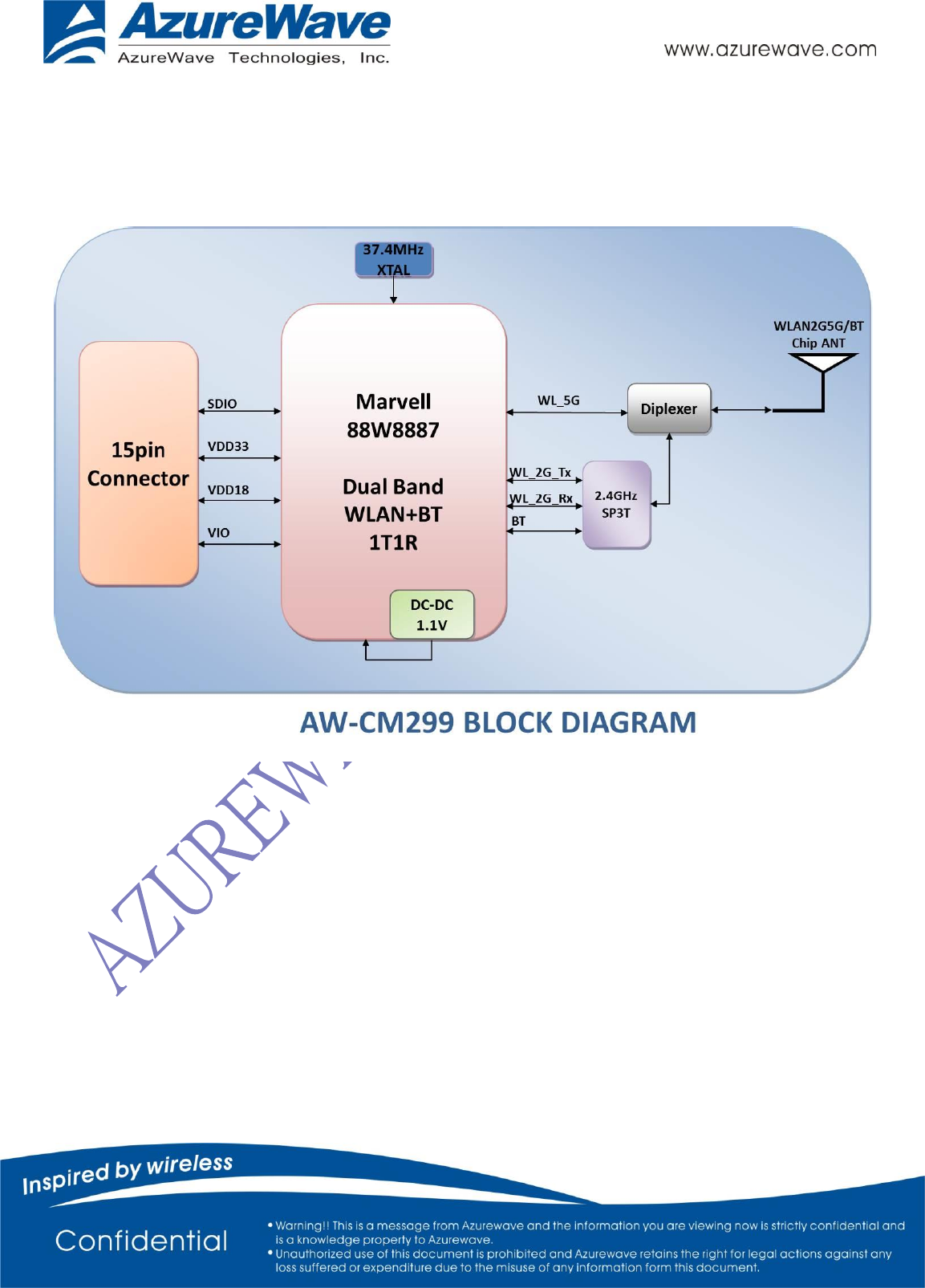
1-2. Block Diagram
A simplified block diagram of the AW-CM299 module is depicted in the figure below.

- 5 -
1-3. Key feature:
Small footprint: 22mm(L) x 11mm(W) x 2.3mm(H)Max
IEEE 802.11ac compliant, 1x1 spatial stream with data rates up to MCS9 (433 Mbps)
Bluetooth 4.2 (supports Low Energy (LE))
SDIO 3.0 device interface may be used as host interface for WLAN/Bluetooth
On board dual band chip antenna
Multiple power saving modes for low power consumption
Lead-free design
- 6 -
1-4. Specifications Table
Model Name
AW-CM299
Product Description
Wireless LAN + Bluetooth Combo Module
WLAN Standard
IEEE 802.11ac/a/b/g/n, Wi-Fi compliant
Bluetooth Standard
Bluetooth 4.2 complaint with Bluetooth 2.1+Enhanced Data Rate (EDR)
Host Interface
SDIO 3.0 device interface (SPI, 1-bit SDIO, 4-bit SDIO transfer
modes at full clock range up to 208 MHz)
Major Chipset
Marvell 88W8887
Dimension
22mm x 11mm x 2.3mm(Max)
Weight
TBD
Antenna
On Board Chip Antenna
Operating Conditions
Voltage
3.3V/1.8V+- 10%
Temperature
Operating: -20 ~ 85oC ; Storage: -40 ~ 85oC
Electrical Specifications
Frequency Range
2.4 GHz ISM radio band / 5 GHz Unlicensed National Information
Infrastructure (U-NII) band
Number of Channels
802.11a: USA, Taiwan – 12/4
Most European Countries –19
Japan – 4
802.11b: USA, Canada and Taiwan – 11
Most European Countries – 13
France – 4
802.11g: USA, Canada and Taiwan – 11
Most European Countries – 13
Japan – 13
802.11n(HT20): Channel 1~13(2412~2472)
802.11n(HT40): Channel 1~7(2422~2472)
Modulation
DSSS,OFDM,DBPSK,DQPSK,CCK, 16-QAM, 64-QAM 256-QAM for WLAN
GFSK (1Mbps), Π/4 DQPSK (2Mbps) and 8DPSK (3Mbps) for Bluetooth
Output Power
WLAN(conducted):
WLAN G band:
11b:16dBm +/- 2dB(11Mbps)
11g:14dBm +/- 2dB (54Mbps)
11n HT20:13dBm +/- 2dB(MCS7)
11n HT40:12dBm +/- 2dB(MCS7)
WLAN A band:
11a:13dBm +/- 2dB(54Mbps)
11n HT20:12dBm +/- 2dB(MCS7)
11n HT40:11dBm +/- 2dB(MCS7)
11ac VHT_20:11dBm +/- 2dB(MCS8)
11ac VHT_40:10dBm +/- 2dB(MCS9)
11ac VHT_80: 7dBm +/- 2dB(MCS9)
Bluetooth(conducted):
BDR/EDR:2dBm+-2dB(class2)
- 7 -
Receive Sensitivity
WLAN(conducted):
WLAN G band :
11b: -87dBm (11Mbps)
-95dBm(1Mbps)
11g: -73dBm (54Mbps)
-88dBm(6Mbps)
11n HT20: -70dBm (MCS7)
-84dBm(MCS0)
11n HT40: -68dBm (MCS7)
-82dBm(MCS0)
WLAN A band:
11a: -68dBm (54Mbps)
-85dBm(6Mbps)
11n HT20: -66dBm (MCS7)
-85dBm(MCS0)
11n HT40: -64dBm(MCS7)
-82dBm(MCS0)
11ac VHT_20: -61dBm(MCS8)
-85dBm(MCS0)
11ac VHT_40: -58dBm(MCS9)
-83dBm(MCS0)
11ac VHT_80: -52dBm(MCS9)
-80dBm(MCS0)
Bluetooth(conducted):
BDR : -80dBm(DH5)
EDR: -80dBm(2DH5)
Data Rates
WLAN
802.11b: 1, 2, 5.5, 11Mbps
802.11a/g: 6, 9, 12, 18, 24, 36, 48, 54Mbps
802.11n: up to 150Mbps
802.11ac:up to 86.7Mbps (20MHz channel)
802.11ac:up to 200Mbps (40MHz channel)
802.11ac:up to 433Mbps (80MHz channel)
Bluetooth
Bluetooth 2.1+EDR data rates of 1,2, and 3Mbps
ESD Rating
HCP/VCP discharge ±4KV
Operating Range
Open Space: ~300m ; Indoor: ~100m for WLAN
Minimum 10 m indoor for Bluetooth
The transmission speed may vary according to the environment)
Security
WAPI
WEP 64-bit and 128-bit encryption with H/W TKIP processing
WPA/WPA2 (Wi-Fi Protected Access)
AES-CCMP hardware implementation as part of 802.11i security
standard
Operating System Compatibility
Linux (Android, Meego), More information please contact Azurewave
FAE.
- 8 -
2. Electrical Characteristic
2-1.Absolute Maximum Ratings
Symbol
Parameter
Condition
Min
Typ
Max
Units
VCC33
3.3V input
--
--
3.3
4.0
V
VCC18
1.8V input
--
--
1.8
2.2
V
VIO
Host I/O power supply
--
--
3.3
4.0
V
2.5
3.0
1.8
2.2
2-2.Recommanded Operating Conditions
Symbol
Parameter
Condition
Min
Typ
Max
Units
VCC33
LDO VBAT input
--
2.7
3.3
3.63
V
VCC18
1.8V power supply
--
1.71
1.8
1.89
V
VIO
1.8V/2.5V/3.3V digital I/O
power supply
--
2.97
3.3
3.63
V
2.25
2.5
2.75
1.62
1.8
1.98
- 9 -
2-3.Clock Specifications
2-3-1 External Sleep Clock Timing
External Sleep Clock is necessary for two reasons:
1. Auto frequency Detection.
This is where the internal logic will bin the Ref clock source to figure out what is the reference clock
frequency is. This is done so no strapping is needed for telling 8887 what the ref clock input is.
2. Allow low current modes for BT to enter sleep modes such as sniff modes.
The AW-CM299 external sleep clock pin is powered from the 1.8V voltage supply.
Symbol
Parameter
Min
Typ
Max
Units
CLK
Clock Frequency Range
32 or 32.768 -50ppm
32 or 32.768
32 or 32.768 +50ppm
KHz
THIGH
Clock high time
40
--
--
ns
TLOW
Clock low time
40
--
--
ns
TRISE
Clock rise time
--
--
5
ns
TFALL
Clock fall time
--
--
5
ns
2-4. Reset Configuration
The AW-CM299 is reset to its default operating state under the following conditions:
Power-on reset (POR)
Software/Firmware reset
External pin reset (RESETn)
2-4-1. Internal Reset
The AW-CM299 device is reset, and the internal CPU begins the boot sequence when any of the following internal
reset events occur:
Device receives power and VDDL supplies rise (triggers internal POR circuit)
External pin (PDn) assertion will generate POR
2-4-2.
External
Reset
The AW-CM299 is reset when PDn pin is asserted low and the internal CPU begins the boot sequence when the
PDn pin transitions from low to high.
- 10 -
3. Host Interfaces
3-1. SDIO Interface
The AW-CM299 supports a SDIO device interface that conforms to the industry standard SDIO Full-Speed card
specification and allows a host controller using the SDIO bus protocol to access the Wireless module device.
The AW-CM299 acts as the device on the SDIO bus. The host unit can access registers of the SDIO interface
directly and can access shared memory in the device through the use of BARs and a DMA engine.
The SDIO device interface main features include:
Supports SDIO 3.0 Standard
On-chip memory used for CIS
Supports SPI, 1-bit SDIO, and 4-bit SDIO transfer modes
Special interrupt register for information exchange
Allows card to interrupt host
3-1-1. SDIO Interface Signal Description
Pin Name
Signal
Name
Type
Description
SD_CLK
CLK
I/O
SDIO 1-bit mode: Clock
SDIO SPI mode: Clock
SD_CMD
CMD
I/O
SDIO 1-bit mode: Command line
SDIO SPI mode: Data input
SD_DAT[3]
DAT3
I/O
SDIO 4-bit mode: Data line bit [3]
SDIO 1-bit mode: Not used
SDIO SPI mode: Chip select (active low)
SD_DAT[2]
DAT2
I/O
SDIO 4-bit mode: Data line bit [2] or Read Wait (optional)
SDIO 1-bit mode: Read Wait (optional)
SDIO SPII mode: Reserved
SD_DAT[1]
DAT1
I/O
SDIO 4-bit mode: Data line bit [1]
SDIO 1-bit mode: Interrupt
SDIO SPI mode: Interrupt
SD_DAT[0]
DAT0
I/O
SDIO 4-bit mode: Data line bit [0]
SDIO 1-bit mode: Data line
SDIO SPI mode: Data output
- 11 -
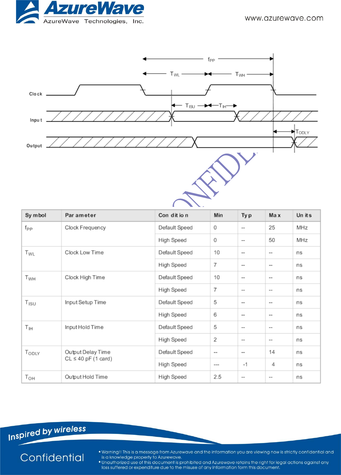
3-1-2. Default Speed, High Speed Modes (3.3V)
SDIO Protocol Timing Diagram – Default Speed Mode (3.3V)
SDIO Protocol Timing Diagram – HighSpeed Mode (3.3V)
Table shows SDIO Timing Data—Default Speed, High Speed Modes (3.3V)
NOTE: Over full range of values specified in the Recommended Operating Conditions unless otherwise specified.
- 12 -
4. Pin Definition
Pin No
Definition
Basic Description
Type
1
VCC33_1
Main Power Supply (3.3V)
I
2
VCC33_2
Main Power Supply (3.3V)
I
3
VCC18
1.8V Power Supply
I
4
VIO
1.8V/3.3V I/O Power Supply
I
5
GND_5
GND
-
6
PDn
Power Down (H : normal operation, L : power down)
Pulled up to VIO
I
7
BT_wakeup_host
Bluetooth wakeup host
O
8
SD_DATA0
SDIO DATA0
I/O
9
SD_DATA1
SDIO DATA1
I/O
10
SD_DATA2
SDIO DATA2
I/O
11
SD_DATA3
SDIO DATA3
I/O
12
SD_CMD
SDIO Command
I/O
13
GND_13
GND
-
14
SD_CLK
SDIO CLOCK
I
15
GND_15
GND
-
- 13 -
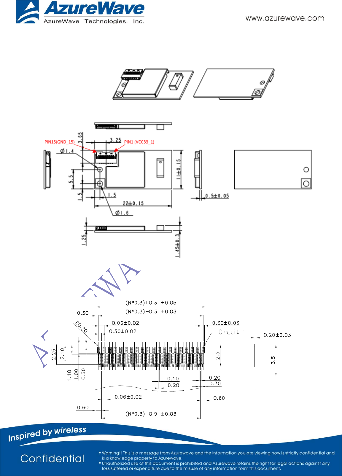
5. Mechanical Information
5-1. Package Outline Drawing
5-2. Recommended FPC/FFC
- 14 -
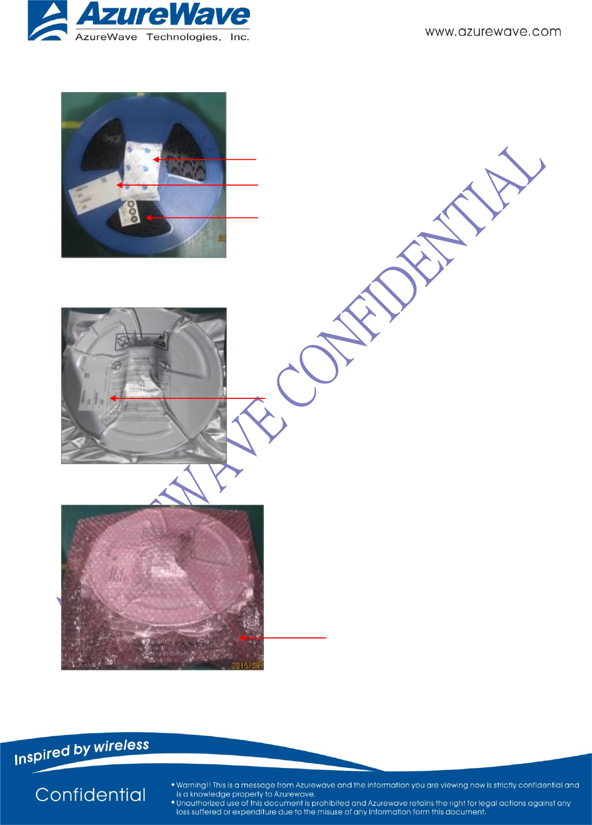
6. Shipping Information
6-1
6-2
6-3
6-4
1 UNIT DESICCANT
HUMIDITY INDICATOR CARD
AFFIX PACKING LABEL
AFFIX PACKING LABEL
PINK BUBBLE WRAP
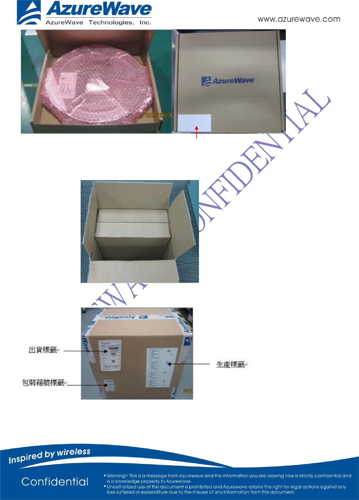
- 15 -
6-5
1 Carton= 3 Boxes
6-6
Note: 1 tape reel = 1 box = 1,100pcs
1 carton = 3 boxes = 3 * 1,100pcs= 3,300pcs
AFFIX PACKING LABEL
生产标签
- 16 -
7. Federal Communication Commission Interference Statement
This equipment has been tested and found to comply with the limits for a Class B digital device,
pursuant to Part 15 of the FCC Rules. These limits are designed to provide reasonable
protection against harmful interference in a residential installation. This equipment generates,
uses and can radiate radio frequency energy and, if not installed and used in accordance with
the instructions, may cause harmful interference to radio communications. However, there is no
guarantee that interference will not occur in a particular installation. If this equipment does
cause harmful interference to radio or television reception, which can be determined by turning
the equipment off and on, the user is encouraged to try to correct the interference by one of the
following measures:
- Reorient or relocate the receiving antenna.
- Increase the separation between the equipment and receiver.
- Connect the equipment into an outlet on a circuit different from that
to which the receiver is connected.
- Consult the dealer or an experienced radio/TV technician for help.
FCC Caution: Any changes or modifications not expressly approved by the party responsible for
compliance could void the user's authority to operate this equipment.
This device complies with Part 15 of the FCC Rules. Operation is subject to the following two
conditions: (1) This device may not cause harmful interference, and (2) this device must accept
any interference received, including interference that may cause undesired operation.
IMPORTANT NOTE:
Radiation Exposure Statement:
This equipment complies with FCC radiation exposure limits set forth for an uncontrolled environment. This
equipment should be installed and operated with minimum distance 20cm between the radiator & your body.
This transmitter must not be co-located or operating in conjunction with any other antenna or
transmitter.
Country Code selection feature to be disabled for products marketed to the US/CANADA
- 17 -
This device is intended only for OEM integrators under the following conditions:
1) The antenna must be installed such that 20 cm is maintained between the antenna and
users, and
2) The transmitter module may not be co-located with any other transmitter or antenna,
3) For all products market in US, OEM has to limit the operation channels in CH1 to CH11
for 2.4G band by supplied firmware programming tool. OEM shall not supply any tool or
info to the end-user regarding to Regulatory Domain change.
As long as 3 conditions above are met, further transmitter test will not be required. However, the
OEM integrator is still responsible for testing their end-product for any additional compliance
requirements required with this module installed
IMPORTANT NOTE
In the event that these conditions can not be met (for example certain laptop configurations or
co-location with another transmitter), then the FCC authorization is no longer considered valid
and the FCC ID can not be used on the final product. In these circumstances, the OEM
integrator will be responsible for re-evaluating the end product (including the transmitter) and
obtaining a separate FCC authorization.
End Product Labeling
This transmitter module is authorized only for use in device where the antenna may be installed
such that 20 cm may be maintained between the antenna and users. The final end product must
be labeled in a visible area with the following: “Contains FCC ID: TLZ-CM299”.
Manual Information to the End User
The OEM integrator has to be aware not to provide information to the end user regarding how to
install or remove this RF module in the user’s manual of the end product which integrates this
module.
The end user manual shall include all required regulatory information/warning as show in this
manual.