AzureWave Technologies CU302 IEEE 802.11 b/g/n + Bluetooth 4.2 LE WLAN/BT Microcontroller Module User Manual AW CU302 datasheet V0 7x
AzureWave Technologies, Inc. IEEE 802.11 b/g/n + Bluetooth 4.2 LE WLAN/BT Microcontroller Module AW CU302 datasheet V0 7x
User Manual
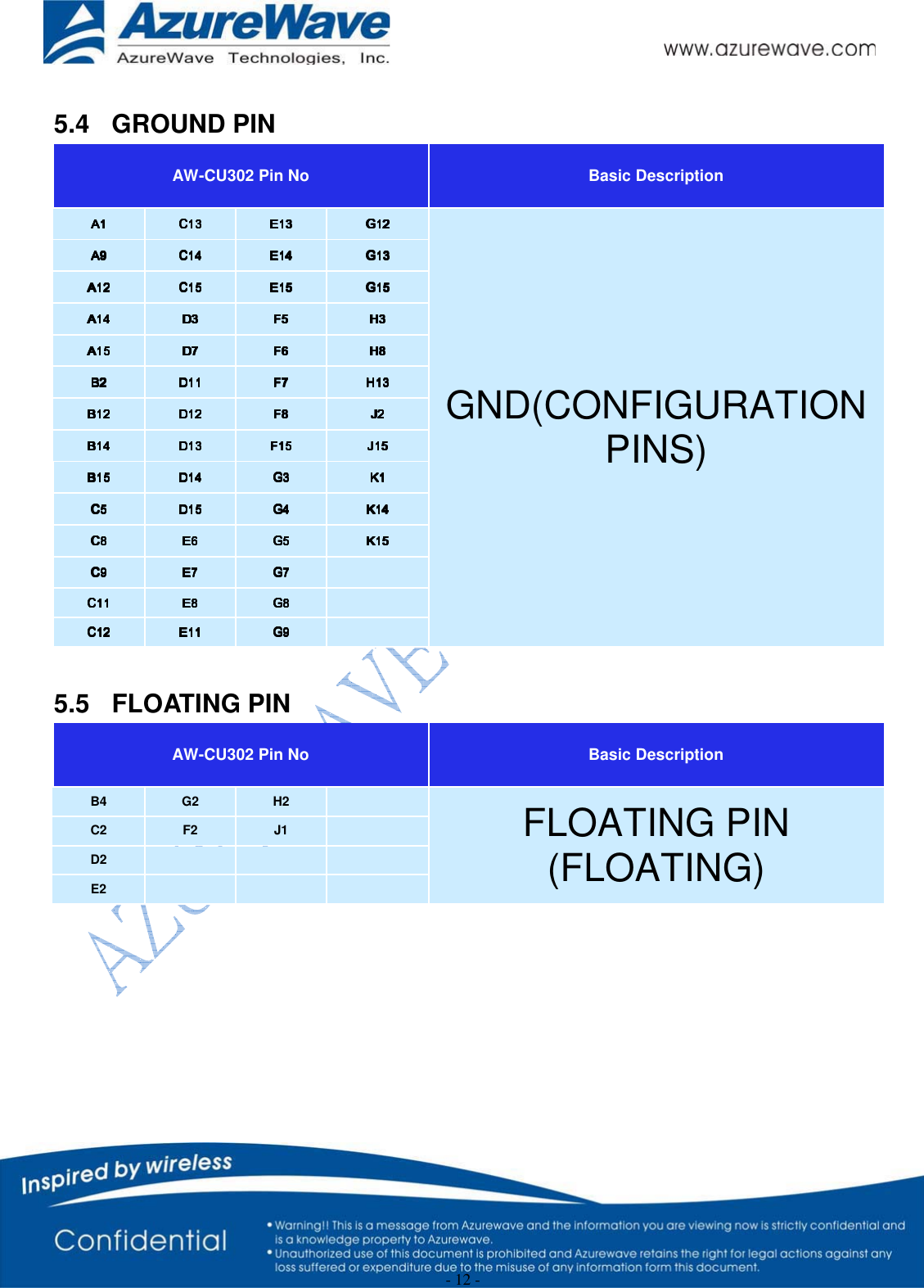
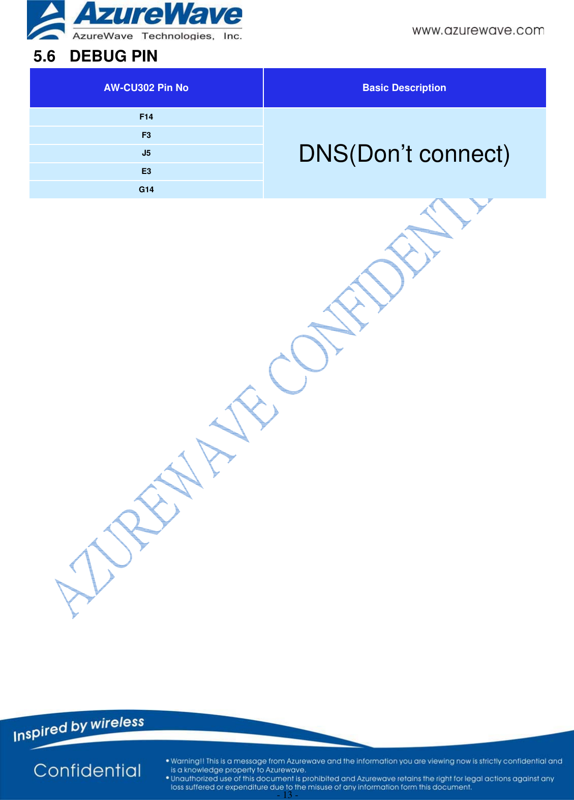
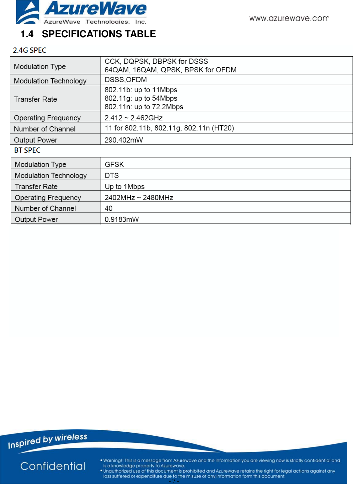
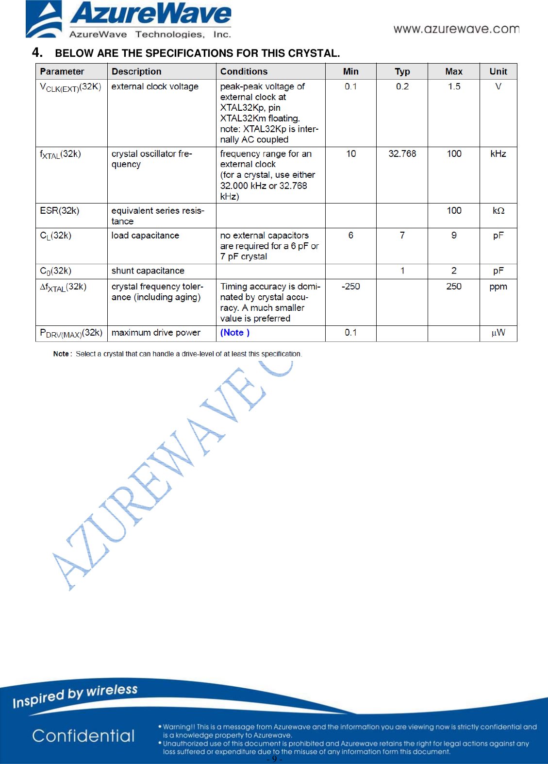
![- 3 - Index 1.GENERAL DESCRIPTION ............................................................................................................... 41.1PRODUCT OVERVIEW AND FUNCTIONAL DESCRIPTION ................................................ 41.2KEY FEATURES .................................................................................................................... 51.3FUNCTION BLOCK ............................................................................................................... 61.4SPECIFICATIONS TABLE ..................................................................................................... 72.ELECTRICAL CHARACTERISTICS ............................................................................................. 82.1ABSOLUTE MAXIMUM RATINGS ......................................................................................... 82.2RECOMMENDED OPERATING CONDITIONS ..................................................................... 82.3INTERNAL MEMORY ............................................................................................................ 82.4EXTERNAL 32KHZ CRYSTAL REQUIREMENTS ................................................................. 83.APPLICATION: .................................................................................................................................. 84.BELOW ARE THE SPECIFICATIONS FOR THIS CRYSTAL. ................................................. 95.PIN DEFINITION ............................................................................................................................. 105.1POWER PIN ........................................................................................................................ 105.2GPIO [88MW300] PIN .......................................................................................................... 105.3GPIO [DA14580] PIN ........................................................................................................... 115.4GROUND PIN ...................................................................................................................... 125.5FLOATING PIN .................................................................................................................... 125.6DEBUG PIN ......................................................................................................................... 136.CONFIGURATION PINS ................................................................................................................ 146.1POWER PIN ........................................................................................................................ 146.2CLOCK [88MW300] PIN ...................................................................................................... 146.3GROUND PIN ...................................................................................................................... 147.MECHANICAL CHARACTERISTICS ......................................................................................... 15](https://usermanual.wiki/AzureWave-Technologies/CU302/User-Guide-3594608-Page-3.png)
![- 10 - 5. PIN DEFINITION 5.1 POWER PIN Pin No Definition Basic Description Type Level A10 VBAT_WL_3V3 88MW300/FLASH power supply. (Pin A10 with Pin B10 configuration) A, I 3.3V B10 VBAT_WL_3V3 88MW300/FLASH power supply. (Pin A10 with Pin B10 configuration) A, I 3.3V A11 VBAT_BT_3V3 DA14580 power supply. (Pin A11 with B11 configuration) A, I 3.3V B11 VBAT_BT_3V3 DA14580 power supply. (Pin A11 with B11 configuration) A, I 3.3V A13 VPP_BT_6V8 This pin is used while DA14580 OTP programming and testing. OTP programming: VPP = 6.7 V ± 0.1 V OTP Normal operation: leave VPP floating A, I 6.8V 5.2 GPIO [88MW300] PIN Pin No Definition Function 0 Function 1 Function 2 Function 3 Function 4 Function 5 Type Level J4 GPIO_0 GPIO_0 GPT0_CH0 UART0_CTS SSP0_CLK I/O 3.3V J6 GPIO_1 GPIO_1 GPT0_CH1 UART0_RTS SSP0_FRM I/O 3.3V K7 GPIO_2(4) GPIO_2 GPT0_CH2 UART0_TXD SSP0_TXD I/O 3.3V K6 GPIO_3(4) GPIO_3 GPT0_CH3 UART0_RXD SSP0_RXD I/O 3.3V B7 GPIO_4 GPIO_4 GPT0_CH4 I2C0_SDA AUDIO_CLK I/O 3.3V A4 GPIO_5 GPIO_5 GPT0_CH5 I2C0_SCL I/O 3.3V B5 GPIO_7(2) JTAG TCK GPIO_7 UART2_CTS SSP2_CLK I2C0_SDA I/O 3.3V A5 GPIO_8(2) JTAG TMS GPIO_8 UART2_RTS SSP2_FRM I2C0_SDL I/O 3.3V A6 GPIO_10 JTAG TRST GPIO_10 UART2_RXD SSP2_RXD I2C1_SDL I/O 3.3V E1 GPIO_16(1) GPIO_16 CON[5] AUDIO_CLK I/O 3.3V A3 GPIO_23 WAKE_UP_1 GPIO_23 UART0_CTS COMP_IN_P I/O 3.3V B1 GPIO_24(3) OCS32K GPIO_24 UART0_RXD GPT1_CH5 COMP_IN_N I/O 3.3V C1/J9 GPIO_25(3) XTAL32K_IN GPIO_25 I2C1_SDA I/O 3.3V D1 GPIO_26(3) XTAL32K_OUT GPIO_26 I2C1_SCL I/O 3.3V F1 GPIO_27(1) GPIO_27 CON[4] UART0_TXD I/O 3.3V H1 GPIO_40 GPIO_40 ADC_DAC_TRIGGER0 ACOMP0_GPIO_OUT ACOMP1_GPIO_OUT I/O 3.3V G1 GPIO_41 GPIO_41 ADC_DAC_TRIGGER1 ACOMP0_EDGE_PULSE ACOMP1_EDGE_PULSE I/O 3.3V K4 GPIO_46 GPIO_46 ADC_4/ ACOMP4 UART2_CTS SSP2_CLK I/O 3.3V](https://usermanual.wiki/AzureWave-Technologies/CU302/User-Guide-3594608-Page-8.png)
![- 11 - K2 GPIO_47 GPIO_47 ADC_5/ ACOMP5 UART2_RTS SSP2_FRM I/O 3.3V K3 GPIO_48 GPIO_48 ADC_6/ ACOMP6 UART2_TXD SSP2_TXD I/O 3.3V K5 GPIO_49 GPIO_49 ADC_7/ ACOMP7 UART2_RXD SSP2_RXD I/O 3.3V A2 RESETN_WL RESETn Host reset I 3.3V(internal pull high 51k ohm) *(1) Configuration Pins Table: AW-CU302 Pin No Definition Function 1 Description (Configuration Bits) F1 GPIO_27 88MW300 Boot Options with CON[4], CON[5] 00 = boot from UART 11 = boot from internal QSPI Flash (default) E1 GPIO_16 *(2) 32k clock reference (sleep clock) - External crystal-oscillator driving 32.768 KHz clock to GPIO_25 - External crystal connected to GPIO_25 & GPIO_26 at 32.768 KHz - Connect GPIO_24 to GPIO_25 for calibration reference to RC32K *(3) SWD support on GPIO_7 (SWDCLK) and GPIO_8 (SWDIO) *(4) Console UART0 on GPIO_2 (TXD) and GPIO_3 (RXD) 5.3 GPIO [DA14580] PIN Pin No Definition Function Type Level J11 GPIO_0_0_BT Support ADC[0]. Pull-down enabled during and after reset. General purpose I/O port bit or alternate function nodes. AIO 3.3V J10 GPIO_0_1_BT Support ADC[1]. Pull-down enabled during and after reset. General purpose I/O port bit or alternate function nodes. AIO 3.3V J8 GPIO_0_6_BT Pull-down enabled during and after reset. General purpose I/O port bit or alternate function nodes. I/O 3.3V H12 GPIO_1_0_BT Pull-down enabled during and after reset. General purpose I/O port bit or alternate function nodes. I/O 3.3V K9 GPIO_1_1_BT Pull-down enabled during and after reset. General purpose I/O port bit or alternate function nodes. I/O 3.3V K13 GPIO_2_3_BT Pull-down enabled during and after reset. General purpose I/O port bit or alternate function nodes. I/O 3.3V J13 GPIO_2_4_BT Pull-down enabled during and after reset. General purpose I/O port bit or alternate function nodes. I/O 3.3V B13 GPIO_2_5_BT Pull-down enabled during and after reset. General purpose I/O port bit or alternate function nodes. I/O 3.3V B9 GPIO_2_6_BT Pull-down enabled during and after reset. General purpose I/O port bit or alternate function nodes. I/O 3.3V A8 GPIO_2_7_BT Pull-down enabled during and after reset. General purpose I/O port bit or alternate function nodes. I/O 3.3V B8 GPIO_2_8_BT Pull-down enabled during and after reset. General purpose I/O port bit or alternate function nodes. I/O 3.3V A7 GPIO_2_9_BT Pull-down enabled during and after reset. General purpose I/O port bit or alternate function nodes. I/O 3.3V K8 I 3.3V(internal pull low 2.2k ohm) J12 SWCLK_BT JTAG Data input/output. Bidirectional data and control communication. Can also be used as a GPIO. I/O 3.3V K12 SWDIO_BT INPUT JTAG clock signal. Can also be used as a GPIO. I/O 3.3V K10 XTAL32Kp INPUT. Crystal input for the 32.768kHz XTAL. I 3.3V K11 XTAL32Km OUTPUT. Crystal output for the 32.768kHz XTAL. O 3.3V](https://usermanual.wiki/AzureWave-Technologies/CU302/User-Guide-3594608-Page-9.png)