AzureWave Technologies CU302 IEEE 802.11 b/g/n + Bluetooth 4.2 LE WLAN/BT Microcontroller Module User Manual AW CU302 datasheet V0 7x
AzureWave Technologies, Inc. IEEE 802.11 b/g/n + Bluetooth 4.2 LE WLAN/BT Microcontroller Module AW CU302 datasheet V0 7x
User Manual
- 1 -
AW-CU302
IEEE 802.11 b/g/n + Bluetooth 4.2 LE
WLAN/BT Microcontroller Module
Datasheet
Version 0.7

- 2 -
Document
release Date Modification Initials Approved
Version0.4 2016/11/23 Initial (New Solution) Kai Wu Daniel Lee
Version0.5 2017/3/15
Redesign:
- Support external ANT for WLAN
- Only 3.3V power supply
Kai Wu Daniel Lee
Version0.6 2017/4/1
Redesign:
- RF DPDT switch
- 32.768KHz(Oscillator)
Kai Wu Daniel Lee
Version0.7 2017/8/1
Redesign:
- 32.768KHz(Crystal +Oscillator)
- Added Debug pins
Alex Yu Daniel Lee

- 3 -
Index
1.GENERAL DESCRIPTION ............................................................................................................... 4
1.1PRODUCT OVERVIEW AND FUNCTIONAL DESCRIPTION ................................................ 4
1.2KEY FEATURES .................................................................................................................... 5
1.3FUNCTION BLOCK ............................................................................................................... 6
1.4SPECIFICATIONS TABLE ..................................................................................................... 7
2.ELECTRICAL CHARACTERISTICS ............................................................................................. 8
2.1ABSOLUTE MAXIMUM RATINGS ......................................................................................... 8
2.2RECOMMENDED OPERATING CONDITIONS ..................................................................... 8
2.3INTERNAL MEMORY ............................................................................................................ 8
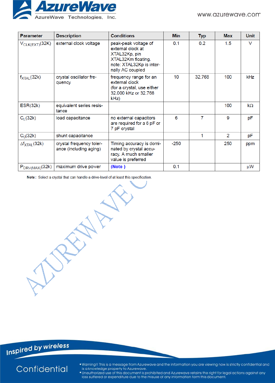
2.4EXTERNAL 32KHZ CRYSTAL REQUIREMENTS ................................................................. 8
3.APPLICATION: .................................................................................................................................. 8
4.BELOW ARE THE SPECIFICATIONS FOR THIS CRYSTAL. ................................................. 9
5.PIN DEFINITION ............................................................................................................................. 10
5.1POWER PIN ........................................................................................................................ 10
5.2GPIO [88MW300] PIN .......................................................................................................... 10
5.3GPIO [DA14580] PIN ........................................................................................................... 11
5.4GROUND PIN ...................................................................................................................... 12
5.5FLOATING PIN .................................................................................................................... 12
5.6DEBUG PIN ......................................................................................................................... 13
6.CONFIGURATION PINS ................................................................................................................ 14
6.1POWER PIN ........................................................................................................................ 14
6.2CLOCK [88MW300] PIN ...................................................................................................... 14
6.3GROUND PIN ...................................................................................................................... 14
7.MECHANICAL CHARACTERISTICS ......................................................................................... 15

- 4 -
1. GENERAL DESCRIPTION
1.1 PRODUCT OVERVIEW AND FUNCTIONAL DESCRIPTION
AzureWave presents AW-CU302 Wi-Fi/BT Microcontroller Smart Energy Platform Solution provides a
highly cost-effective, flexible and easy to-use hardware/software platform to build a new generation of
connected, smart devices. These smart-connected devices enable device to deliver a broad-range of
services to consumers including energy-management, demand-response, home automation and remote
access. This allows a user to manage comfort and convenience, also run diagnostics and receive alerts
and notifications, in addition to managing and controlling the device. Developers can leverage the rich
connectivity features of these new smart devices to create a new generation of innovative new
applications and services
The platform builds upon the success of Marvell’s first-generation Wi-Fi/BT microcontroller platforms
using the Marvell/Dialog 88MW300/DA14580 Wi-Fi/BT System-on-Chip (SoC), a 4MByte QSPI flash
memory and Marvell Easy Connect software.
- 5 -
1.2 KEY FEATURES
MCUs of AW-CU302
g 88MW300 (Marvell 88MW300 is a WLAN IEEE 802.11 b/g/n standalone SoC)
Processor
¾ ARM Cortex-M4F, 32bit
¾ 200MHz main bus clock
Memory
¾ 128KB ROM
¾ 512KB RAM
Flash Controller
¾ 32KB SRAM cache to support XIP
¾ Memory-mapped access to QSPI Flash devices
Wireless
¾ IEEE 802.11 b/g/n HT20
¾ Low-power with deep sleep and standby modes
¾ Fully supports clients (stations) implementing IEEE Power Save mode
¾ Wi-Fi direct connectivity
g DA14580 (Dialog DA14580 is a Bluetooth Low Energy 4.2 SoC)
Processor
¾ ARM Cortex-M0, 32bit, 16MHz
¾ Dedicated Link Layer Processor
¾ AES-128 bit encryption Processor
Memory
¾ 42 KB System SRAM
¾ 84 KB ROM
¾ 8 KB Retention SRAM
Wireless
¾ Bluetooth V4.2
Memory of AW-CU302
g 4M Byte QSPI flash
IO Interfaces
g UART
g SWD(JTAG)
g SSP(SPI)
g GPT(PWM)
g I2C
g ADC
g GPIO
Wireless
g Wi-Fi 802.11 b/g/n only HT20
g Bluetooth V4.2
Package
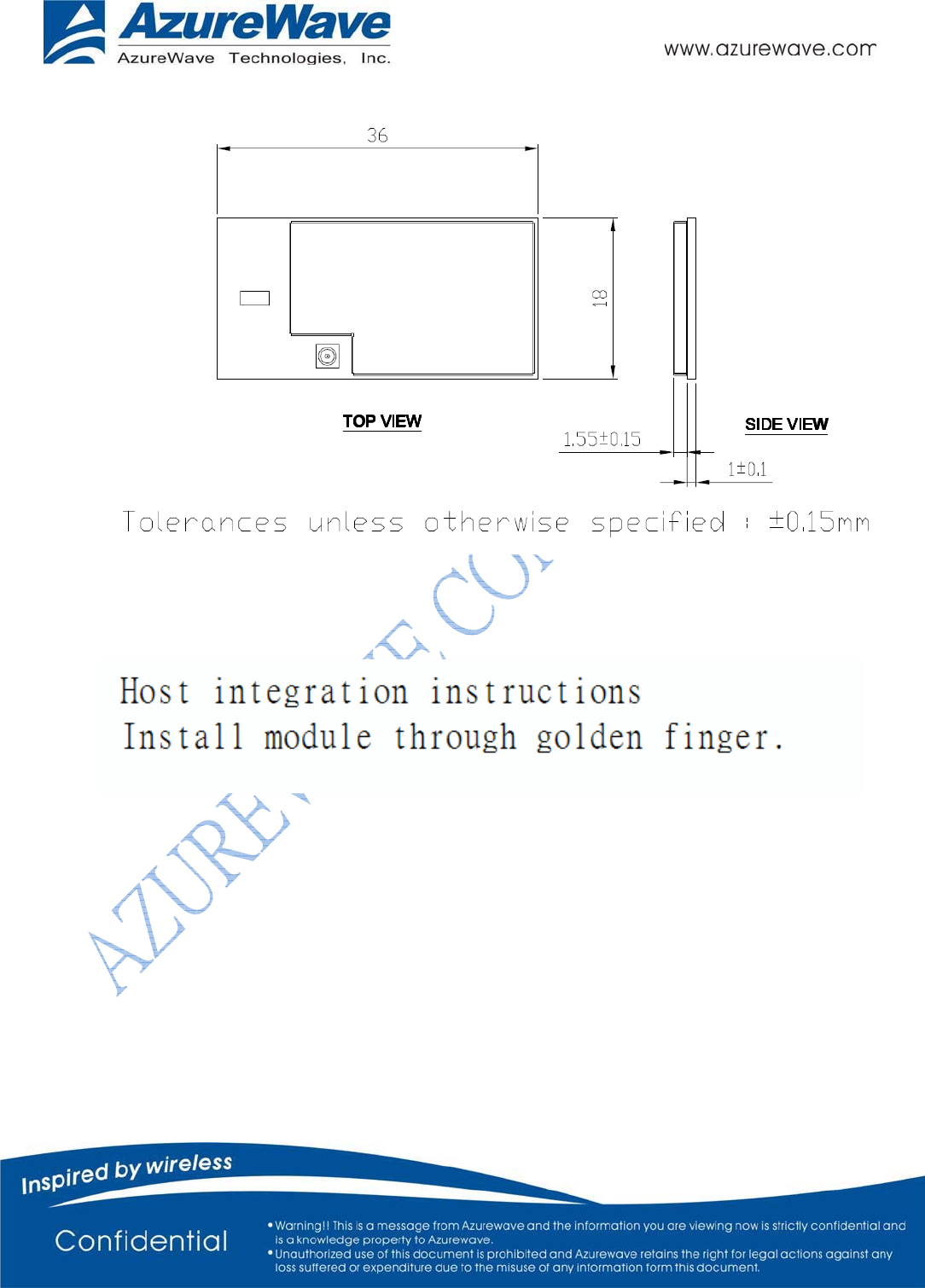
g LGA Module – 36 mm x 18 mm x 2.5 mm 111 pin
Antenna
g Internal Chip Antenna for WLAN/BT coexistence or BT only
g External U.FL connector for WLAN only
Certifications
g TBD
- 7 -
1.4 SPECIFICATIONS TABLE
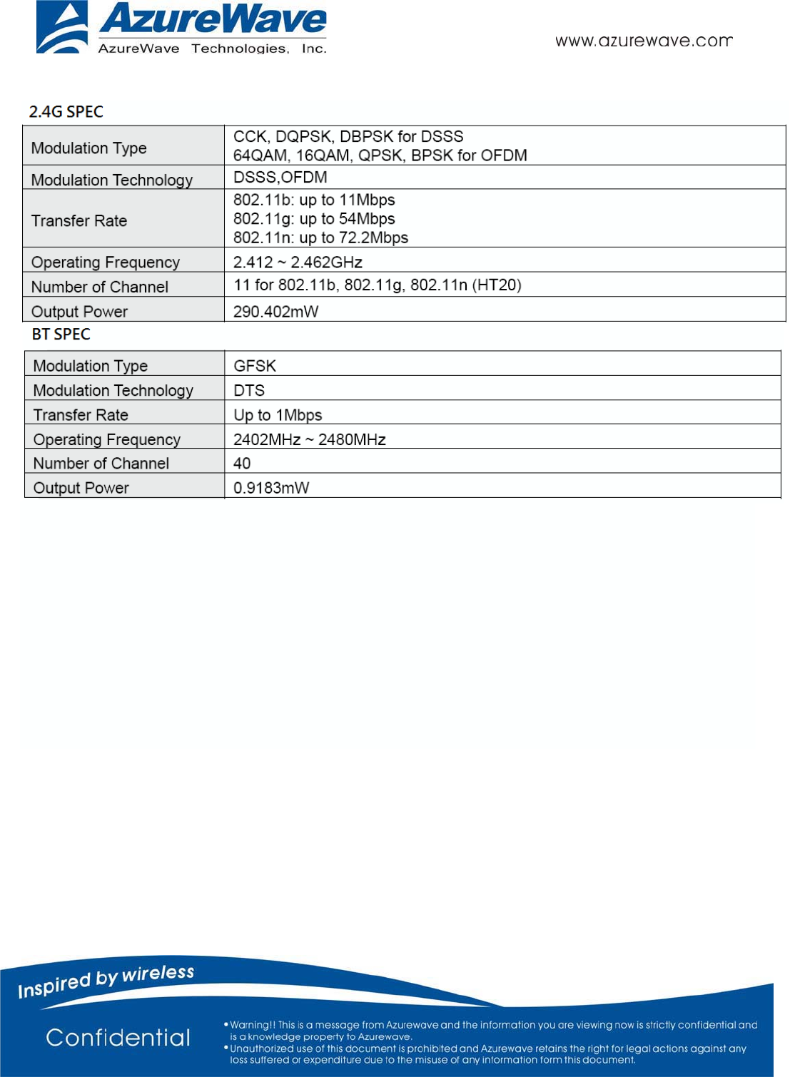
Product Description AW-CU302 Wireless Smart Energy module
WLAN Standard IEEE 802.11b/g/n, Wi-Fi compliant
BT Standard Bluetooth V4.2 complaint
Host Interface UART/JTAG/SSP/I2C/ADC
Major Chipset
Marvell 88MW300 + Dialog DA14580 + 4MB flash
Dimension 36 mm x 18 mm x 2.5 mm
Package 111-pin LGA
Operating Conditions
Voltage 3.3V +/- 9%
Temperature Operating: -30 ~ 85 ; Storage: TBD
Electrical Specifications
Frequency Range 2.4 GHz ISM radio band
Number of Channels
802.11b: Channel 1(2.412GHz)~13(2.472GHz)
802.11g: Channel 1(2.412GHz)~13(2.472GHz)
802.11n(HT20): Channel 1(2.412GHz)~13(2.472GHz)
Modulation DSSS, OFDM, DBPSK, DQPSK, CCK, 16-QAM, 64-QAM for WLAN
GFSK (1Mbps), Ȇ/4 DQPSK (2Mbps) and 8DPSK (3Mbps) for Bluetooth
Output Power
WiFi: FCC/IC 290.402mW
BLE :FCC/IC :0.9183mW
BLE:
-TBD
-
Receive Sensitivity
WLAN:
-TBD
Bluetooth:
-TBD
Antenna
Function1: Internal Chip Antenna for WLAN/BT coexistence.
Function2: Internal Chip Antenna for BT only, u.FL(external antenna) for
WLAN only
Data Rates
WLAN:
802.11b: 1, 2, 5.5, 11Mbps
802.11g: 6, 9, 12, 18, 24, 36, 48, 54Mbps
802.11n: MCS0-7,up to 72.2Mbps(20MHz channel )
Bluetooth:
Bluetooth Low Energy Only
- 9 -
4. BELOW ARE THE SPECIFICATIONS FOR THIS CRYSTAL.
- 10 -
5. PIN DEFINITION
5.1 POWER PIN
Pin No
Definition Basic Description Type Level
A10 VBAT_WL_3V3 88MW300/FLASH power supply. (Pin A10 with Pin B10 configuration) A, I 3.3V
B10 VBAT_WL_3V3 88MW300/FLASH power supply. (Pin A10 with Pin B10 configuration) A, I 3.3V
A11 VBAT_BT_3V3 DA14580 power supply. (Pin A11 with B11 configuration) A, I 3.3V
B11 VBAT_BT_3V3 DA14580 power supply. (Pin A11 with B11 configuration) A, I 3.3V
A13 VPP_BT_6V8
This pin is used while DA14580 OTP programming and testing.
OTP programming: VPP = 6.7 V ± 0.1 V
OTP Normal operation: leave VPP floating
A, I 6.8V
5.2 GPIO [88MW300] PIN
Pin No Definition Function 0 Function 1 Function 2 Function 3 Function 4 Function 5 Type Level
J4 GPIO_0 GPIO_0 GPT0_CH0 UART0_CTS SSP0_CLK I/O 3.3V
J6 GPIO_1 GPIO_1 GPT0_CH1 UART0_RTS SSP0_FRM I/O 3.3V
K7 GPIO_2
(4)
GPIO_2 GPT0_CH2 UART0_TXD SSP0_TXD I/O 3.3V
K6 GPIO_3
(4)
GPIO_3 GPT0_CH3 UART0_RXD SSP0_RXD I/O 3.3V
B7 GPIO_4 GPIO_4 GPT0_CH4 I2C0_SDA AUDIO_CLK I/O 3.3V
A4 GPIO_5 GPIO_5 GPT0_CH5 I2C0_SCL I/O 3.3V
B5 GPIO_7
(2)
JTAG TCK GPIO_7 UART2_CTS SSP2_CLK I2C0_SDA I/O 3.3V
A5 GPIO_8
(2)
JTAG TMS GPIO_8 UART2_RTS SSP2_FRM I2C0_SDL I/O 3.3V
A6 GPIO_10 JTAG TRST GPIO_10 UART2_RXD SSP2_RXD I2C1_SDL I/O 3.3V
E1 GPIO_16
(1)
GPIO_16 CON[5] AUDIO_CLK I/O 3.3V
A3 GPIO_23 WAKE_UP_1 GPIO_23 UART0_CTS COMP_IN_P I/O 3.3V
B1 GPIO_24
(3)
OCS32K GPIO_24 UART0_RXD GPT1_CH5 COMP_IN_N I/O 3.3V
C1/J9 GPIO_25
(3)
XTAL32K_IN GPIO_25 I2C1_SDA I/O 3.3V
D1 GPIO_26
(3)
XTAL32K_OU
T GPIO_26 I2C1_SCL I/O 3.3V
F1 GPIO_27
(1)
GPIO_27 CON[4] UART0_TXD I/O 3.3V
H1 GPIO_40 GPIO_40 ADC_DAC_TR
IGGER0
ACOMP0_GPI
O_OUT
ACOMP1_GPI
O_OUT I/O 3.3V
G1 GPIO_41 GPIO_41 ADC_DAC_TR
IGGER1
ACOMP0_ED
GE_PULSE
ACOMP1_ED
GE_PULSE I/O 3.3V
K4 GPIO_46 GPIO_46 ADC_4/
ACOMP4 UART2_CTS SSP2_CLK I/O 3.3V
- 11 -
K2 GPIO_47 GPIO_47 ADC_5/
ACOMP5 UART2_RTS SSP2_FRM I/O 3.3V
K3 GPIO_48 GPIO_48 ADC_6/
ACOMP6 UART2_TXD SSP2_TXD I/O 3.3V
K5 GPIO_49 GPIO_49 ADC_7/
ACOMP7 UART2_RXD SSP2_RXD I/O 3.3V
A2 RESETN_WL RESETn Host reset I
3.3V(internal
pull high 51k
ohm)
*(1) Configuration Pins Table:
AW-CU302
Pin No Definition Function 1 Description (Configuration Bits)
F1 GPIO_27
88MW300 Boot Options with CON[4], CON[5]
00 = boot from UART
11 = boot from internal QSPI Flash (default)
E1 GPIO_16
*(2) 32k clock reference (sleep clock)
- External crystal-oscillator driving 32.768 KHz clock to GPIO_25
- External crystal connected to GPIO_25 & GPIO_26 at 32.768 KHz
- Connect GPIO_24 to GPIO_25 for calibration reference to RC32K
*(3) SWD support on GPIO_7 (SWDCLK) and GPIO_8 (SWDIO)
*(4) Console UART0 on GPIO_2 (TXD) and GPIO_3 (RXD)
5.3 GPIO [DA14580] PIN
Pin No Definition Function Type Level
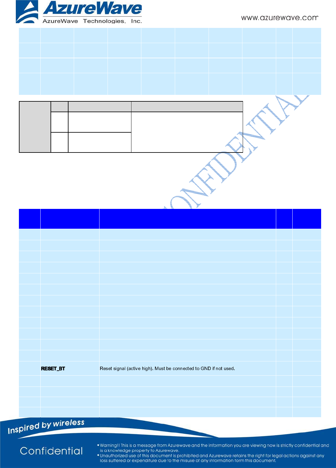
J11 GPIO_0_0_BT Support ADC[0]. Pull-down enabled during and after reset. General purpose
I/O port bit or alternate function nodes. AIO 3.3V
J10 GPIO_0_1_BT Support ADC[1]. Pull-down enabled during and after reset. General purpose
I/O port bit or alternate function nodes. AIO 3.3V
J8 GPIO_0_6_BT Pull-down enabled during and after reset. General purpose I/O port bit or
alternate function nodes. I/O 3.3V
H12 GPIO_1_0_BT Pull-down enabled during and after reset. General purpose I/O port bit or
alternate function nodes. I/O 3.3V
K9 GPIO_1_1_BT Pull-down enabled during and after reset. General purpose I/O port bit or
alternate function nodes. I/O 3.3V
K13 GPIO_2_3_BT Pull-down enabled during and after reset. General purpose I/O port bit or
alternate function nodes. I/O 3.3V
J13 GPIO_2_4_BT Pull-down enabled during and after reset. General purpose I/O port bit or
alternate function nodes. I/O 3.3V
B13 GPIO_2_5_BT Pull-down enabled during and after reset. General purpose I/O port bit or
alternate function nodes. I/O 3.3V
B9 GPIO_2_6_BT Pull-down enabled during and after reset. General purpose I/O port bit or
alternate function nodes. I/O 3.3V
A8 GPIO_2_7_BT Pull-down enabled during and after reset. General purpose I/O port bit or
alternate function nodes. I/O 3.3V
B8 GPIO_2_8_BT Pull-down enabled during and after reset. General purpose I/O port bit or
alternate function nodes. I/O 3.3V
A7 GPIO_2_9_BT Pull-down enabled during and after reset. General purpose I/O port bit or
alternate function nodes. I/O 3.3V
K8 I 3.3V(internal
pull low 2.2k
ohm)
J12 SWCLK_BT JTAG Data input/output. Bidirectional data and control communication. Can
also be used as a GPIO. I/O 3.3V
K12 SWDIO_BT INPUT JTAG clock signal. Can also be used as a GPIO. I/O 3.3V
K10 XTAL32Kp INPUT. Crystal input for the 32.768kHz XTAL. I 3.3V
K11 XTAL32Km OUTPUT. Crystal output for the 32.768kHz XTAL. O 3.3V
- 12 -
5.4 GROUND PIN
AW-CU302 Pin No Basic Description
GND(CONFIGURATION
PINS)
5.5 FLOATING PIN
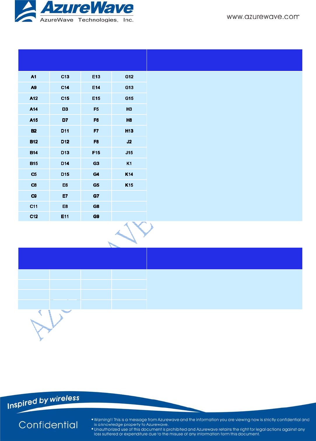
AW-CU302 Pin No Basic Description
B4 G2 H2
FLOATING PIN
(FLOATING)
C2 F2 J1
D2
E2
- 13 -
5.6 DEBUG PIN
AW-CU302 Pin No Basic Description
F14
DNS(Don’t connect)
F3
J5
E3
G14
- 16 -
- AW-CU302 Drawing
Federal Communication Commission Interference Statement
This device complies with Part 15 of the FCC Rules. Operation is subject to the following
two conditions: (1) This device may not cause harmful interference, and (2) this device
must accept any interference received, including interference that may cause undesired
operation.
This equipment has been tested and found to comply with the limits for a Class B digital
device, pursuant to Part 15 of the FCC Rules. These limits are designed to provide
reasonable protection against harmful interference in a residential installation. This
equipment generates, uses and can radiate radio frequency energy and, if not installed and
used in accordance with the instructions, may cause harmful interference to radio
communications. However, there is no guarantee that interference will not occur in a
particular installation. If this equipment does cause harmful interference to radio or
television reception, which can be determined by turning the equipment off and on, the
user is encouraged to try to correct the interference by one of the following measures:
- Reorient or relocate the receiving antenna.
- Increase the separation between the equipment and receiver.
- Connect the equipment into an outlet on a circuit different from that
to which the receiver is connected.
- Consult the dealer or an experienced radio/TV technician for help.
FCC Caution: Any changes or modifications not expressly approved by the party
responsible for compliance could void the user's authority to operate this equipment.
This transmitter must not be co-located or operating in conjunction with any other antenna
or transmitter.

Radiation Exposure Statement:
This equipment complies with FCC radiation exposure limits set forth for an uncontrolled
environment. This equipment should be installed and operated with minimum distance
20cm between the radiator & your body.
This device is intended only for OEM integrators under the following conditions:
The antenna must be installed such that 20 cm is maintained between the antenna and
users, and
The transmitter module may not be co-located with any other transmitter or antenna.
As long as 2 conditions above are met, further transmitter test will not be required.
However, the OEM integrator is still responsible for testing their end-product for any
additional compliance requirements required with this module installed
IMPORTANT NOTE: In the event that these conditions can not be met (for example
certain laptop configurations or co-location with another transmitter), then the FCC
authorization is no longer considered valid and the FCC ID can not be used on the final
product. In these circumstances, the OEM integrator will be responsible for re-evaluating
the end product (including the transmitter) and obtaining a separate FCC authorization.
End Product Labeling
This transmitter module is authorized only for use in device where the antenna may be
installed such that 20 cm may be maintained between the antenna and users. The final end
product must be labeled in a visible area with the following: “Contains FCC ID:
”. The grantee's FCC ID can be used only when all FCC compliance
requirements are met.
Manual Information To the End User
The OEM integrator has to be aware not to provide information to the end user regarding
how to install or remove this RF module in the user’s manual of the end product which
integrates this module.
The end user manual shall include all required regulatory information/warning as show in
this manual.
Industry Canada statement:
This device complies with ISED’s licence-exempt RSSs. Operation is subject to the
following two conditions: (1) This device may not cause harmful interference, and (2) this
device must accept any interference received, including interference that may cause
undesired operation.
Le présent appareil est conforme aux CNR d’ ISED applicables aux appareils radio
exempts de licence. L’exploitation est autorisée aux deux conditions suivantes : (1) le
dispositif ne doit pas produire de brouillage préjudiciable, et (2) ce dispositif doit accepter
tout brouillage reçu, y compris un brouillage susceptible de provoquer un fonctionnement
indésirable.
Radiation Exposure Statement:
This equipment complies with ISED radiation exposure limits set forth for an
uncontrolled environment. This equipment should be installed and operated with
minimum distance 20cm between the radiator & your body.
Déclaration d'exposition aux radiations:
Cet équipement est conforme aux limites d'exposition aux rayonnements ISED établies
pour un environnement non contrôlé. Cet équipement doit être installé et utilisé avec un
minimum de 20 cm de distance entre la source de rayonnement et votre corps.
This device is intended only for OEM integrators under the following conditions: (For
module device use)㻌
1) The antenna must be installed such that 20 cm is maintained between the antenna and
users, and
2) The transmitter module may not be co-located with any other transmitter or antenna.
As long as 2 conditions above are met, further transmitter test will not be required.
However, the OEM integrator is still responsible for testing their end-product for any
additional compliance requirements required with this module installed.
Cet appareil est conçu uniquement pour les intégrateurs OEM dans les conditions suivantes:
(Pour utilisation de dispositif module)
1) L'antenne doit être installée de telle sorte qu'une distance de 20 cm est respectée entre
l'antenne et les utilisateurs,
2) Le module émetteur peut ne pas être coïmplanté avec un autre émetteur ou antenne.
Tant que les 2 conditions ci-dessus sont remplies, des essais supplémentaires sur
l'émetteur ne seront pas nécessaires. Toutefois, l'intégrateur OEM est toujours responsable
des essais sur son produit final pour toutes exigences de conformité supplémentaires
requis pour ce module installé.
IMPORTANT NOTE:
In the event that these conditions can not be met (for example certain laptop
configurations or co-location with another transmitter), then the Canada authorization is
no longer considered valid and the IC ID can not be used on the final product. In these
circumstances, the OEM integrator will be responsible for re-evaluating the end product
(including the transmitter) and obtaining a separate Canada authorization.
NOTE IMPORTANTE:㻌
Dans le cas où ces conditions ne peuvent être satisfaites (par exemple pour certaines
configurations d'ordinateur portable ou de certaines co-localisation avec un autre
émetteur), l'autorisation du Canada n'est plus considéré comme valide et l'ID IC ne peut
pas être utilisé sur le produit final. Dans ces circonstances, l'intégrateur OEM sera chargé
de réévaluer le produit final (y compris l'émetteur) et l'obtention d'une autorisation
distincte au Canada.
End Product Labeling
This transmitter module is authorized only for use in device where the antenna may be
installed such that 20 cm may be maintained between the antenna and users. The final end
product must be labeled in a visible area with the following: “Contains IC: ”.
Plaque signalétique du produit final
Ce module émetteur est autorisé uniquement pour une utilisation dans un dispositif où
l'antenne peut être installée de telle sorte qu'une distance de 20cm peut être maintenue
entre l'antenne et les utilisateurs. Le produit final doit être étiqueté dans un endroit visible
avec l'inscription suivante: "Contient des IC: ".
Manual Information To the End User
The OEM integrator has to be aware not to provide information to the end user regarding
how to install or remove this RF module in the user’s manual of the end product which
integrates this module.
The end user manual shall include all required regulatory information/warning as show in
this manual.
Manuel d'information à l'utilisateur final
L'intégrateur OEM doit être conscient de ne pas fournir des informations à l'utilisateur
final quant à la façon d'installer ou de supprimer ce module RF dans le manuel de
l'utilisateur du produit final qui intègre ce module.
Le manuel de l'utilisateur final doit inclure toutes les informations réglementaires requises
et avertissements comme indiquǪ dans ce manuel.

ե
եфႝݢᒟ܄ႝᐒᆅᒤݤ
ಃΜΒచ ࠠԄᇡӝϐեфᓎႝᐒǴߚёǴϦљǵဦ܈
٬Ҕޣ֡όளᏰԾᡂ׳ᓎǵуεф܈ᡂ׳চीϐ܄Ϸ
фૈǶ
ಃΜѤచ եфᓎႝᐒϐ٬Ҕόளቹៜ०ૐӼӄϷυᘋӝݤ೯ߞǹ
วԖυᘋຝਔǴᔈҥջଶҔǴ٠ׯ๓ԿคυᘋਔБளᝩុ
٬ҔǶ
ӝݤ೯ߞǴࡰ٩ႝߞݤೕۓբϐคጕႝ೯ߞǶ
եфᓎႝᐒהڙӝݤ೯ߞ܈πǵࣽᏢϷᙴᕍҔႝݢᒟ
܄ႝᐒഢϐυᘋǶ
1. ҁኳಔܭڗளᇡࡕஒ٩ೕۓܭኳಔҁᡏҢቩᡍӝᠸǶ
2. سቷᔈܭѳѠҢȨҁౢࠔϣ֖ᓎኳಔǺ
XXXyyyLPDzzzz-xȩӷኬǶ