B plus B SmartWorx WLRG601 802.11 b/g radio module User Manual
B&B; Electronics 802.11 b/g radio module
User Manual

Product Specification
802.11b/g SDIO/SPI Airborne Radio
WLRG-RA-DP600 Family
Revision: 2.4
June 2010
File name: wlrg-ra-dp601 product brief v2.4
Document Number: 846-8310-240
Product Brief – Airborne SDIO/SPI 802.11b/g Radio Quatech, Inc.
846-8310-240 June 2010 2
1.0 Product Description
The WLNG-RA-DP600 family is a Marvell 88W8686 based 802.11b/g SDIO/SPI radio,
designed by Quatech, to support handheld, mobile station and other power sensitive
applications. The radio features the following:
802.11b/g radio
Based upon Marvell Libertas 88W8686 Chipset
30 pin high density SMT connector (Molex 53748-0308)
Single (1) Hirose U.FL RF connector for 802.11b/g
Supports WEP, WPA, WPA2 (Home and Enterprise) and 802.1x Supplicants
Bluetooth Co-existence 3-wire interface through main connector
SDIO 1.0 and Generic SPI host interface through 30 pin header
Operating Temperature (-30°C to 85°C)
Storage temp (-30°C to 125°C)
Advanced Low power modes
High vibration mounting holes
Supports host downloaded radio firmware
Single antenna
Driver support for WinCE 5.0, Windows Mobile 5.0/6.0, Linux 2.6 and other
embedded OS‟s
Small form factor radio module (Dimensions: 29mm x 21mm x 6.0mm)
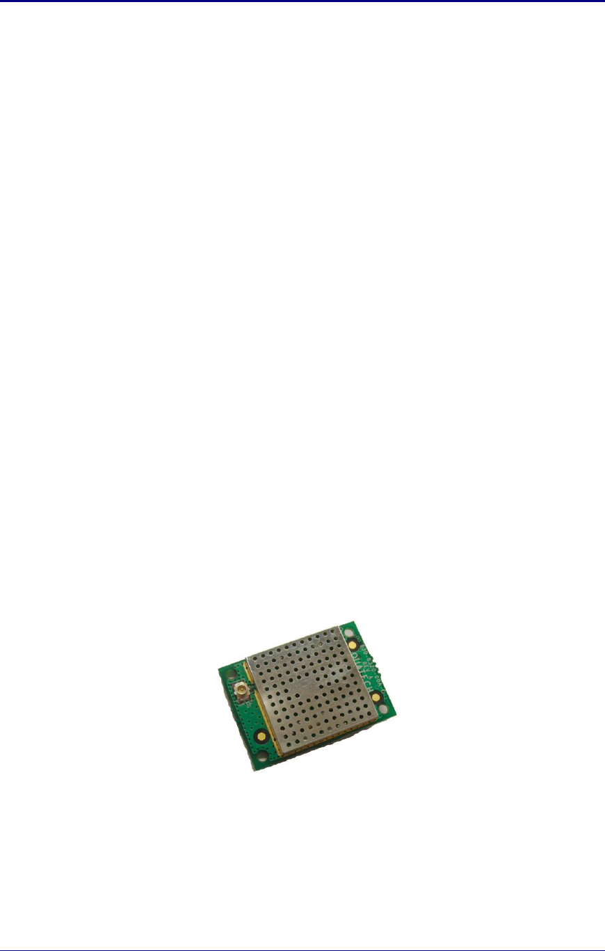
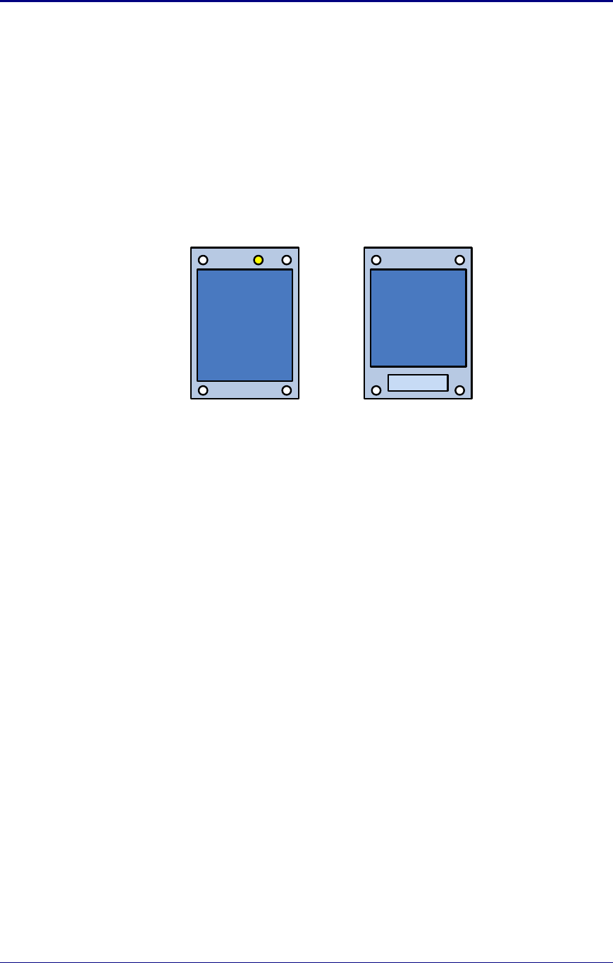
Figure 1- Lakemore Radio Example
Product Brief – Airborne SDIO/SPI 802.11b/g Radio Quatech, Inc.
846-8310-240 June 2010 3
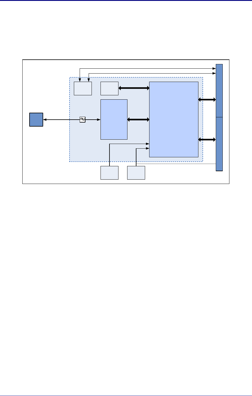
2.0 Block Diagram
The following outlines the block diagram of the radio:
Marvell
88W8686 IEEE 802.11 MAC
Processor & RF Transciever
SDIO/SPI Interface
Power
Management
32.768KHz
Xtal Oscillator
40 MHz
Xtal Oscillator
802.11b/g FEM
U.FL RF
Connector
VDD (3.3VDC)
BT Coexistence
Serial
EEPROM
802.11b/g RF
VHIO (1.8VDC or VDD)
External Sleep Clock Option Available
Product Brief – Airborne SDIO/SPI 802.11b/g Radio Quatech, Inc.
846-8310-240 June 2010 4
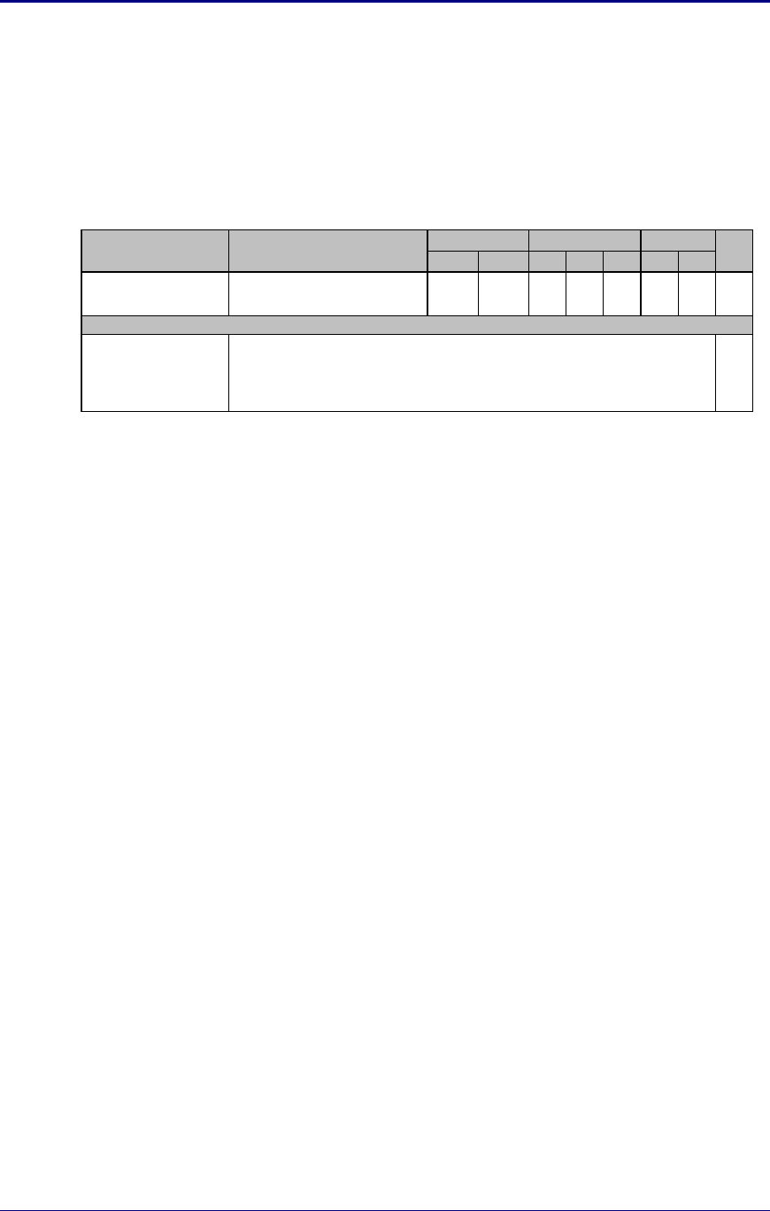
3.0 Model Numbers
The following table identifies the model numbers associated with the radio family. Please
contact Quatech sales for details, quotes and availability.
Table 1 - Model Numbers
802.11b 802.11g SDIO SPI BT Co VDD VHIO
WLRG-RA-DP601
802.11b/g, SDIO/SPI, Bluetooth
Coexistence, VDD & VHIO supply
(Lakemore)
l l
l1l1llll
WLEG-RA-DP601
802.11b/g SDIO/SPI Radio Eval Kit
WLRG-RA-DP601 radio
SDIO Adapter Card
Tools/Documentation CD
Drivers (WinCE/Linux/XP)
l
Notes: 1. Interface selection through pin 5 (SDIO) on main conector.
2. Radio supports external sleep oscillator option. Please contact Quatech sales for more information.
3. The Bluetooth Coexistance interface does not include RF antenna sharing option. For more details contact Quatech sales.
RoHS
Eval Kit
Model Number
WiFi
Interface
Supply
Description
Product Brief – Airborne SDIO/SPI 802.11b/g Radio Quatech, Inc.
846-8310-240 June 2010 5
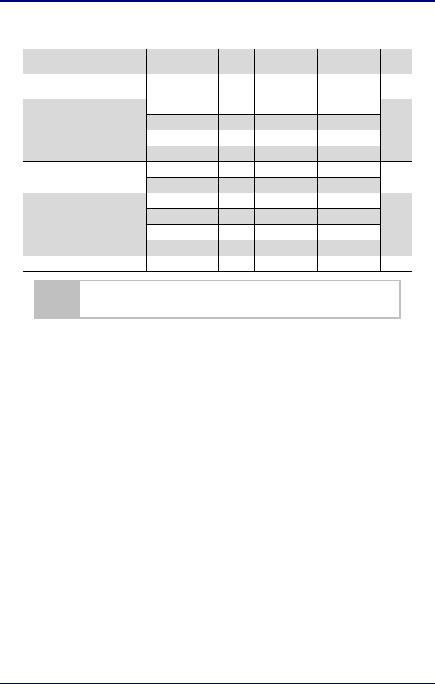
4.0 Pin out and Connectors
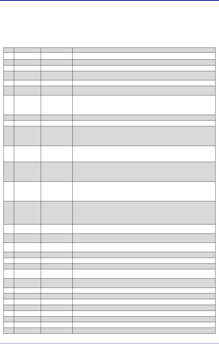
Table 2 – Radio Pin Definition
Pin
Signal
Pin I/O Type
Description
1
GND
Ground
2
GND
Ground
3
DNC
Reserved pin, DO NOT CONNECT
4
VHIO
Supply Input
Host Digital I/O Supply voltage for SDIO/SPI and Bluetooth interfaces.
VHIO = 1.8VDC or VDD. Internally decoupled to GNDHIO.
5
SDIO
Digital Input
Serial Host mode. SPI = GND, SDIO = VDD
6
VHIO
Supply Input
Host Digital I/O Supply voltage for SDIO/SPI and Bluetooth interfaces.
VHIO = 1.8VDC or VDD. Internally decoupled to GNDHIO.
7
DATA2
Digital I/O
SDIO Bit 2 (VHIO Domain)
SDIO 4-bit: Data bit 2 or Read Wait (Optional)
SDIO 1-bit: Read Wait (Optional)
SDIO SPI: Reserved
SPI: SPI Interrupt output (active low)
8
GND
Ground
9
GND
Ground
10
DATA1
Digital I/O
SDIO Bit 1 (VHIO Domain)
SDIO 4-bit: Data bit 1
SDIO 1-bit: Interrupt
SDIO SPI: Reserved
SPI: Data Output
11
DATA3
Digital I/O
SPI/SDIO Card Select (Active Low) (VHIO Domain)
SDIO 4-bit: Data bit 3
SDIO 1-bit: Reserved
SDIO SPI: Card Select (Active Low)
12
SERCLK
Digital Input
SPI/SDIO Clock from host(VHIO Domain)
SDIO 4-bit: Clock input
SDIO 1-bit: Clock Input
SDIO SPI: Clock Input
SPI: Clock Input
13
DATA0
Digital I/O
SDIO Bit 0 (VHIO Domain)
SDIO 4-bit: Data bit 0
SDIO 1-bit: Data Line
SDIO SPI: Data Output
SPI: SPI Device Select (Active Low)
14
CMD
Digital Input
SPI/SDIO data input for 4-Wire mode, data input/output for 3-wire mode. (VHIO Domain)
SDIO Command/Response
SDIO 4-bit: Command/response
SDIO 1-bit: Command
SDIO SPI: 4-wire = Data Input. 3-wire = Data I/O
SPI: Data Input
15
VDD
Analog Supply
Input
Supply Voltage (3.3VDC)
16
WLNAPU
Digital Input
(Pull Down)
Card Power Up Enable from Host (active High). Internal Pull-up.
17
VDD
Analog Supply
Input
Supply Voltage (3.3VDC)
18
SPI_RSTn
Digital Input
SPI Device RESET from MCU. Active Low
19
RF_ACTIVE
Digital Input
Asserted by the BT device during Rx or Tx slots that it wishes to use.
20
DNC
Reserved pin, DO NOT CONNECT
21
TXCONF
Digital Output
Transmission confirmed. Pulled low when the radio wants to prevent the BT device‟s use of the
medium
22
STATUS
Digital Input
Pulsed if the BT device has a priority need for the slot. After that it indicates the BT radio mode (Tx or
RX)
23
DNC
Reserved pin, DO NOT CONNECT
24
MCU_WAKEUP
Digital Output
MCU “wake up” request to the host. Active high. (GPIO5)
25
NC/SLEEPCLK
No connect, optional SLEEPCLK pin for host sourced sleep clock.
26
MAC_WAKEUP
Digital Input
WLAN MAC “wake-up”/interrupt from the host MCU. Active high (GPIO4)
27
UARTSIN
1.8V UART
UART Serial Input.
28
UARTSOUT
1.8V UART
UART Serial Output.
29
GND
Ground
30
GND
Ground
Product Brief – Airborne SDIO/SPI 802.11b/g Radio Quatech, Inc.
846-8310-240 June 2010 6
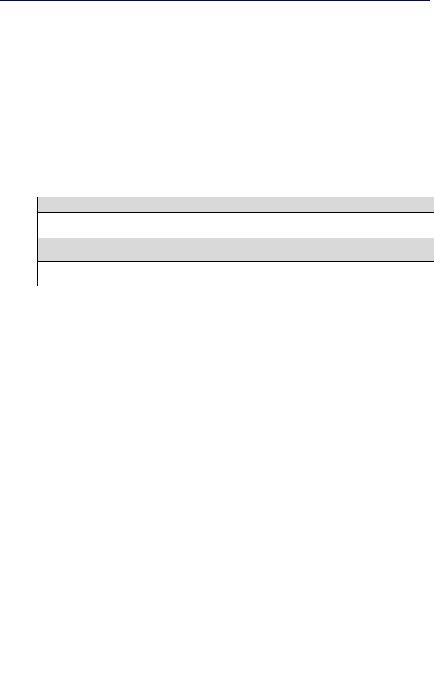
Table 3 - SDIO Interface Definition Table
SDIO
Pin
Module
Pin
SD 4-bit Pin Name
SD 4-bit Description
SD 1-bit Pin Name
SD 1-bit Description
1
11
DATA3
Data bit 3
N/C
Reserved
2
14
CMD
Command line.
CMD
Command line.
3
1, 2, 8,9,
29, 30
VSS1
Ground (GND)
VSS1
Ground
4
4, 6
VDD
Supply Voltage (VHIO)
VDD
Supply Voltage (VHIO)
5
12
CLK
Clock from host (up to 48MHz)
CLK
Clock from host (up to 48MHz)
6
1, 2, 8,9,
29, 30
VSS2
Ground (GND)
VSS2
Ground
7
13
DATA0
Data bit 0
DATA
Data line
8
10
DATA1
Data bit 1
IRQ
Interrupt
9
7
DATA2
Data bit 2
RW
Read/Write (optional)
Table 4 - SPI Interface Definition table
Module Pin
SPI Pin Name
SPI Description
7
DATA2
SPI Host Interrupt Request. Asserted by card to request an SPI data
transfer. Interrupt output.
10
DATA1
SPI Data Output (MISO).
12
CLK
Clock from host (up to TBD MHz)
13
DATA0
SPI Card Select from host. Active Low
14
CMD
SPI Data Input (MOSI).
18
SPI_RSTn
SPI Device RESET from host. Active Low (Section Error!
Reference source not found.)
1. It is recommended pins 27 and 28 be brought out to test pads or a pinned header.
Product Brief – Airborne SDIO/SPI 802.11b/g Radio Quatech, Inc.
846-8310-240 June 2010 7
There are a total of two connectors to the radio:
J1: 30 pin Digital SDIO/SPI Host interface to radio Baseband processor.
Molex: 0537480308 (0.50mm (.020") Pitch SlimStack™Plug, Surface Mount,
Dual Row, Vertical, 3.00mm (.118") Stack Height, 30 Circuits)
J2: RF connector for 802.11b/g antenna.
Hirose U.FL.
RF Shield
J2
Top View Bottom
View
J1
Component
Area
Product Brief – Airborne SDIO/SPI 802.11b/g Radio Quatech, Inc.
846-8310-240 June 2010 8
5.0 Electrical & RF Specification (Preliminary)
Table 5- Absolute Maximum Values1
Parameter
Min
Max
Unit
Maximum EMU Supply Voltage
-0.3
7.0
VDC
Power Dissipation
2.00
W
Operating Temperature Range2
-30
85
oC
Storage Temperature
-50
125
oC
1. These are absolute ratings; exceeding these values may cause permanent damage to the device.
2. Device is operational over full temperature range, however will provide reduced RF compatibility. Fully
compliant temperature range -10C to 85C.
Table 6 – Operating Conditions & DC Specification
Symbol
Parameter
Min
Typ
Max
Units
VDD
Supply Voltage
2.97
3.30
3.63
V
VHIO
Host SDIO Interface supply1
1.62
1.86
1.98
V
IVHIO
SDIO/SPI host interface supply current
VHIO=3.3VDC
8.4
10
mA
ICCTXB
Constant transmit current (802.11b)
Transmitting @ 11Mb/s
218
263
mA
ICCRXB
Constant receive current (802.11b)
Receiving valid packets @ 11MB/s
146
164
mA
ICCTXG
Constant transmit current (802.11g)
Transmitting @ 54Mb/s
161
276
mA
ICCRXG
Constant receive current (802.11g)
Receiving valid packets @ 54MB/s
174
200
mA
ISBIEEE
IEEE Power Save Mode
Associated, Idle, Beacon Interval =
100ms
6
9
mA
ISBPS
Deep power save mode
440
A
ISBFPD
Full power down mode
160
A
1. When VHIO is not 1.8VDC, use VDD parameter for signal levels (VHIO=VDD).
Product Brief – Airborne SDIO/SPI 802.11b/g Radio Quatech, Inc.
846-8310-240 June 2010 9
Table 7 - SDIO/SPI Interface Electrical Characteristics
Symbol
Parameter
Min
Typ
Max
Units
VIHSDIO
Input HIGH Voltage
VCC=MAX, MIN
0.7 VHIO
VHIO+0.3
V
VILSDIO
Input LOW voltage
VCC=MIN, MAX
0
0.3 VHIO
V
VOHSDIO
Output HIGH Voltage
IOL = 0.2mA,
VCC=MIN
VHIO-0.2
VHIO
V
VOLSDIO
Output LOW voltage
IOL = 6mA, VCC=MIN
0
0.6
V
ILSDIO
Input Leakage Current
VCC=MAX,
Input = 0V or VCC
-1
1
A
CINSDIO
Input Capacitance
TBD
pF
COUTSDIO
Output Capacitance
TBD
pF
Table 8 - Supported Data Rates by Band
Band
Supported Data Rates (Mbps)
802.11b
11, 5.5, 2, 1
802.11g
54, 48, 36, 24, 18, 12, 9, 6
Table 9 - Operating Channels
Band
Region
Freq Range
(GHz)
No. of
Channels
Channels
802.11b
US/Canada
2.4 - 2.4835
11
1 - 11
Europe
2.4 - 2.4835
13
1 - 13
France
2.4 - 2.4835
4
10 - 13
Japan
2.4 - 2.497
14
1 - 14
802.11g
US/Canada
2.4 - 2.4835
11
1 - 11
Europe
2.4 - 2.4835
13
1 - 13
France
2.4 - 2.4835
4
10 - 13
Japan
2.4 - 2.497
13
1 - 13
1. Channel count denotes number of non-overlapping channels.
Product Brief – Airborne SDIO/SPI 802.11b/g Radio Quatech, Inc.
846-8310-240 June 2010 10
Table 10 - RF Characteristics – 802.11b/g
Symbol
Parameter
Rate (Mbps)
Min
Average
dBm / mW
Peak
dBm / mW
Units
POUTB
Transmit Power
Output 802.11b
11, 5.5, 2, 1
13.2
20.1
18.2
66.1
dBm
POUTG
Transmit Power
Output 802.11g
48, 54
12.8
19.1
17.3
53.7
dBm
24, 36
12.7
18.6
17.2
52.5
12, 18
12.8
19.1
17.3
53.7
6, 9
12.5
17.8
17.0
50.1
PRSENB
Receive Sensitivity
802.11b
11
-89
dBm
1
-92
PRSENG
Receive Sensitivity
802.11g
54
-72
dBm
36
-78
18
-83
6
-88
FRANGEBG
Frequency Range
2412
2484
MHz
1. All values measured at TA.

Product Brief – Airborne SDIO/SPI 802.11b/g Radio Quatech, Inc.
846-8310-240 June 2010 11
6.0 Antenna
The unit supports antenna connection through a single Hirose U.FL connector, located on
the top surface of the radio next to the RF shielding.
Any antenna used with the system must be designed for operation within the 2.4GHz
ISM band and specifically must support the 2.412GHz to 2.482GHz for 802.11b/g
operation. They are required to have a VSWR of 2:1 maximum referenced to a 50
system impedance.
6.1 Antenna Selection
The Airborne radio supports a number of antenna options, all of which require
connection to the U.FL connectors on the radio. Ultimately the antenna option
selected will be determined by a number of factors, these include consideration
of the application, mechanical construction and desired performance. Since the
number of possible combinations is endless we will review some of the more
common solutions in this section. If your application is not covered during this
discussion please contact Technical Support for more specific answers.
The available antenna connections include:
Host board mounted antenna
Host Chassis mounted antenna
Embedded antenna
In addition to the above options, location and performance need to be
considered, the following sections discuss these items.
6.2 Host Board Mounted Antenna
Host board mounted requires that an antenna connection is physically mounted
to the host system board. It also requires that the host board include a U.FL
connector (two (2) if diversity is being used) to allow a U.FL to U.FL coaxial lead
to connect from the radio to the host board. It will then require 50 matched PCB
traces to be routed from the U.FL connector to the antenna mount.
There are several sources for the U.FL to U.FL coaxial cable these include
Hirose, Sunridge and IPEX. Please contact Quatech for further part numbers and
supply assistance.
This approach can simplify assembly but does require that the host system
configuration can accommodate an antenna location that is determined by the
host PCB. There are also limitations on the ability to seal the enclosure when
using this approach.
This approach also restricts the selection of available antenna. When using this
approach antennas that screw or press fit to the PCB mount connector must be
used. There are many options for the antenna connector type, however if you
wish to utilize the FCC/IOC modular approval the connector choice must comply
with FCC regulations, these state a non-standard connector is required e.g.

Product Brief – Airborne SDIO/SPI 802.11b/g Radio Quatech, Inc.
846-8310-240 June 2010 12
TNC/SMA are not allowed (there are more that are not), RP-TNC/RP-SMA are
allowed.
6.3 Host Chassis Mounted Antenna
Host Chassis mounted antennas require no work on the host PCB. They utilize
an antenna type called „flying lead‟. There are two types of flying leads; one
which provides a bulkhead mounted antenna connector and one which provides
a bulk head mounted antenna. The type you choose will be determined by the
application.
A flying lead system connects a U.FL coaxial lead to the radio‟s U.FL connector,
the other end of the coax is attached to either a bulkhead mounted antenna
connector or directly to an antenna that has an integrated bulkhead mount.
In either of the two cases, the use of this approach significantly reduces the
antenna system development effort and provides for greater flexibility in the
available antenna types and placement in the host system chassis.
When using the flying lead antenna (integrated bulk head mounting), there are no
connector choice restrictions for use with the FCC/IOC modular certification.
However if the flying lead connector is used, the same restrictions as identified
for the Host Mounted Antenna apply.
There are many suppliers of flying lead antenna and connectors; Quatech‟s
Airborne Antenna product line offers a range of antenna solutions.
6.4 Embedded Antenna
Use of Embedded antenna can be the most interesting approach for M2M,
industrial and medical applications. Their small form factor and absence of any
external mounting provides a very compelling argument for their use. There is a
downside to this antenna type and it comes with performance. Antenna
performance for all of the embedded options will, in most cases, be less that that
achievable with external antenna. This does not make them unusable; it will
impact choice of antenna type and requires more focus on placement.
The three main embedded antenna types are PCB embedded, chip (PCB
mounted) and flying lead; each has its advantages and disadvantages (See
Table 11).
Table 11 - Embedded Antenna Options
Antenna Type
Features
Cost
Size
Availability
Performance
PCB Embedded
Lowest
Largest
Custom
Poor
Chip
Low
Small
Standard
Poor
Flying Lead
Low
Small
Standard
Fair

Product Brief – Airborne SDIO/SPI 802.11b/g Radio Quatech, Inc.
846-8310-240 June 2010 13
PCB Embedded – This approach embeds an antenna design into the host PCB.
This approach is very common with add-in WiFi card (CF, PCMCIA, SDIO, etc.)
as it requires no external connections and is the cheapest production approach.
The lower production cost requires significant development cost and lack of
performance and flexibility.
Chip – The integration of a chip antenna is simple and requires a relatively small
footprint on the host system, however, it does suffer from the same limitations of
flexibility and performance seen with the PCB embedded approach. There are
relatively large numbers of suppliers of this type of antenna; there is also a range
of configuration and performance options.
Flying Lead – This approach is similar to the flying lead solution for external
antennas, the difference is that the form factors are smaller and provide a range
of chassis and board mounting options, all for internal use. This approach suffers
less from the performance and flexibility limitations of the other approaches,
since the location of the antenna it not determined by the host PCB design. The
assembly of a system using this approach maybe slightly more complex since
the antenna is not necessarily mounted on the host PCBA.
6.5 Antenna Location
The importance of this design choice cannot be over stressed; it can in fact be
the determining factor between success and failure of the WiFi implementation.
There are several factors that need to be considered when determining location:
Distance of Antenna from radio
Location of host system
Proximity to RF blocking or absorbing materials
Proximity to potential noise or interference
Position relative to infrastructure (Access Points or Laptops)
Orientation of host system relative to infrastructure
Is it known
Is it static
To minimize the impact of the factors above the following things need to be
considered during the development process:
Minimize the distance between the radio and the location of the antenna. The
coaxial cable between the two impacts the Transmit Power and Receive
Sensitivity negatively. Quatech recommends using 1.32-1.37mm outer
diameter U.FL coaxial cables.
Minimize the locations where metal surfaces come into contact or are close
to the location of the antenna.
Avoid locations where RF noise, close to or over lapping the ISM bands, may
occur. This would include microwave ovens and wireless telephone systems
in the 2.4GHz and 5.0GHz frequency range.
Mount the antenna as high on the equipment as possible.

Product Brief – Airborne SDIO/SPI 802.11b/g Radio Quatech, Inc.
846-8310-240 June 2010 14
Locate the antenna where there is a minimum of obstruction between the
antenna and the location of the Access Points. Typically Access Points are
located in the ceiling or high on walls.
Keep the main antenna‟s polarization vertical, or in-line with the antenna of
the Access Points. 802.11 systems utilize vertical polarization and aligning
both transmit and receive antenna maximizes the link quality.
Even addressing all of the above factors, does not guarantee a perfect
connection, however with experimentation an understanding of the best
combination will allow a preferred combination to be identified.
6.6 Performance
Performance is difficult to define as the appropriate metric changes with each
application or may indeed be a combination of parameters and application
requirements. The underlying characteristic that, in most cases, needs to be
observed is the link quality. This can be defined as the bandwidth available over
which communication, between the two devices, can be performed, the lower the
link quality the less likely the devices can communicate.
Measurement of link quality can be made in several ways; Bit Error rate (BER),
Signal to Noise (SNR) ratio, Signal Strength and may also include the addition of
distortion. The link quality is used by the radio to determine the link rate,
generally as the link quality for a given link rate drops below a predefined limit,
the radio will drop to the next lowest link rate and try to communicate using it.
The reciprocal is also true, if the radio observes good link quality at one rate it will
try to move up to the next rate to see if communication can be sustained using it.
It is important to note that for a given position the link quality improves as the link
rate is reduced. This is because as the link rate drops the radios Transmit power
and Receive sensitivity improve.
From this is can be seen the looking at the link rate is an indirect way of
assessing the quality of the link between the device and an Access Point. You
should strive to make the communication quality as good as possible in order to
support the best link rate. However be careful not to over specify the link rate.
Consider your applications bandwidth requirements and tailor your link rate to
optimize the link quality e.g. the link quality for a location at 6Mb/s is better than it
would be for 54Mb/s, if the application only needs 2Mb/s of data throughput, the
6Mb/s rate would provide a better link quality.
Aside from the radio performance, there are a number of other things that
contribute to the link quality; these include the items discussed earlier and
choices made when looking at the overall antenna gain. The antenna gain
contributes to the Equivalent Isotropically Radiated Power (EIRP) of the system.
This is part of an overall measurement of the link quality called link margin.
Link Margin provides a measure of all the parts of the RF path that impact the
ability of two systems to communicate. The basic equation looks like this:

Product Brief – Airborne SDIO/SPI 802.11b/g Radio Quatech, Inc.
846-8310-240 June 2010 15
EIRP (dB) = TxP + TxA – TxC
Link Margin (dB) = EIRP – FPL + (RxS + RxA – RxC)
Where: TxP = Transmitter output power (dBm)
TxA = Transmitter antenna gain (dBi)
TxC = Transmitter to Antenna coax cable loss (dB)
FPL = Free Path Loss (dB)
RxS = Receiver receive sensitivity (dBm)
RxA = Receiver antenna gain (dBi)
RxC = Receiver to Antenna coax cable loss (dB)
This is a complex subject and requires more information that is presented here,
Quatech does recommend at least looking at the subject and evaluating any
system at a basic level.
It is then possible, with a combination of the above items and an understanding
of the application demands, to achieve a link quality optimized for the application
and host design. It is important to note that this is established with a combination
of hardware selection, design choices and configuration of the radio.
Product Brief – Airborne SDIO/SPI 802.11b/g Radio Quatech, Inc.
846-8310-240 June 2010 16
7.0 Bluetooth Coexistence Interface
The Bluetooth coexistence interface implemented on the Airborne 802.11b/g WLRG-RA-
DP600 family of radio‟s is a three wire configuration, designed to support the identified
coexistence recommended practices in the IEEE 802.15.2 standard for the coexistence
of WLAN and Bluetooth devices. This includes collaborative TDMA method described as
Packet Traffic Arbitration (PTA).
The Airborne radio includes a PTA Controller integrated into the BB/MAC processor; this
requires the Bluetooth device to act as a PTA slave to the PTA control module.
Table 12 - BT Interface Pin Definition
Signal
Direction
Description
RF_ACTIVE (Active High)
Input
Asserted by the BT device during Rx or Tx slots that it
wishes to use.
STATUS
Input
Pulsed if the BT device has a priority need for the slot.
After that it indicates the BT radio mode (Tx or RX)
TXCONF (Active Low)
Output
Transmission confirmed. De-asserted when the radio
wants to prevent the BT device‟s use of the medium
Product Brief – Airborne SDIO/SPI 802.11b/g Radio Quatech, Inc.
846-8310-240 June 2010 17
8.0 GSPI Interface
The General Serial Peripheral Interface (GSPI) for the WLRG-RA-DP601 is detailed in
the following section. The interface is powered by the VHIO (pin 4 & 6) supply as defined
in Table 2.
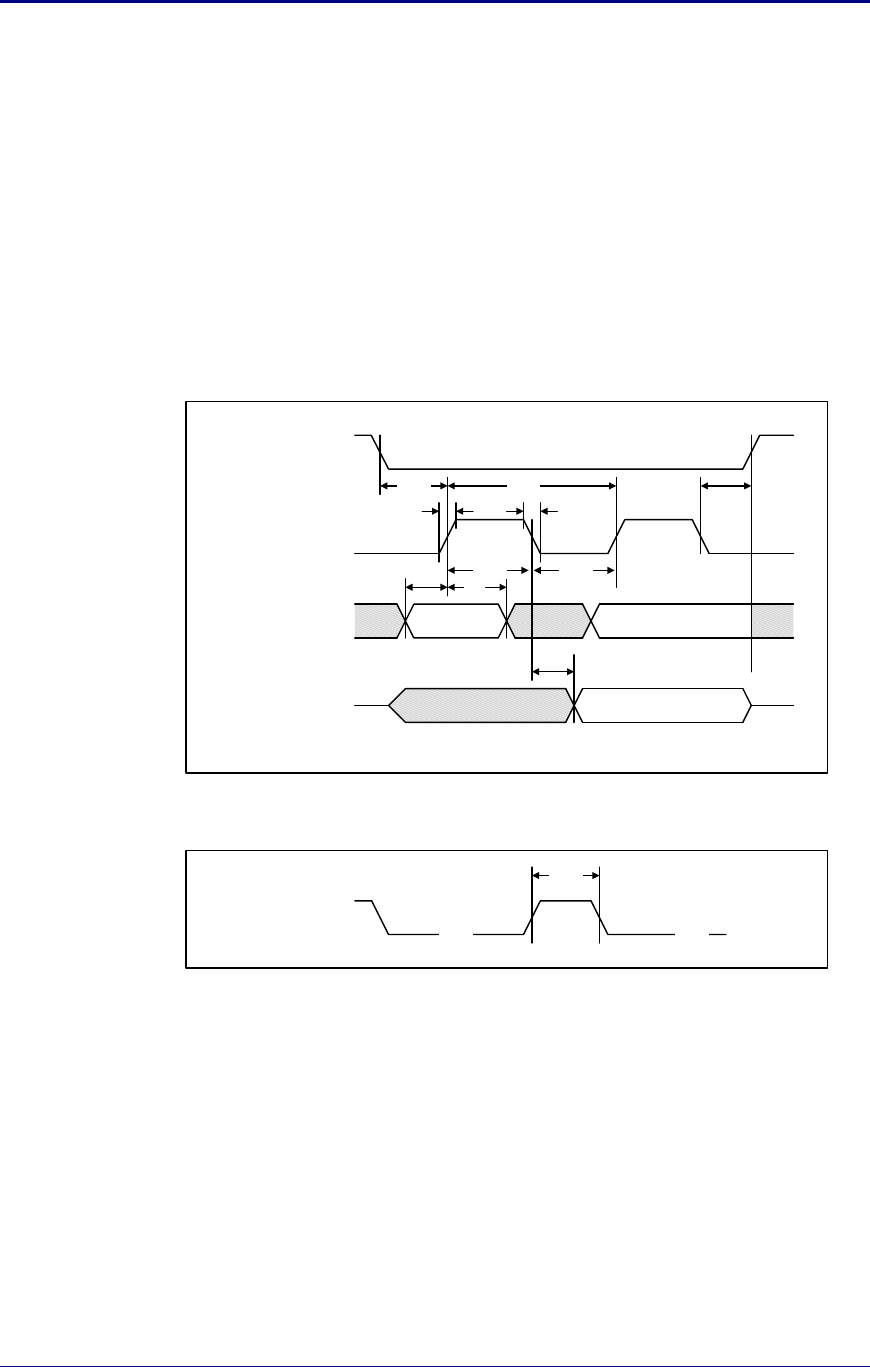
8.1 SPI Protocol Timing
The following figures and table define the required timing for the GSPI interface.
Figure 2 - GSPI Timing Diagram
SPI Clock (CLK)
SPI Select (DATA0)
SPI Data Out (DATA1)
SPI Data In (CMD)
TCSS TSCLK TCSH
TWR TWF
TWH TWL
TSU TH
TV
Hi-Z
VALID DATA IN
Figure 3 - GSPI Inter-Transaction Timing
SPI Select (DATA0)
TCRF
lll lll
Product Brief – Airborne SDIO/SPI 802.11b/g Radio Quatech, Inc.
846-8310-240 June 2010 18
Table 13 - GSPI Protocol Timing Values
Symbol
Parameter
Min
Typ
Max
Units
TSCLK
Clock period
20
ns
TWH
Clock High
5
ns
TWL
Clock Low
9
ns
TWR
Clock Rise Time
1
ns
TWF
Clock Fall Time
1
ns
TH
Serial Data In Hold Time
2.5
ns
TSU
Serial Data In Setup Time
2.5
ns
TV
Serial Data Out Hold Time
5
ns
TCSS
Chip Select Low to Clock
Valid
5
ns
TCSH
Clock Rise or Fall to Chip
Select High
0
ns
TCRF
Chip select High to Chip
Select Low
400
ns
Product Brief – Airborne SDIO/SPI 802.11b/g Radio Quatech, Inc.
846-8310-240 June 2010 19
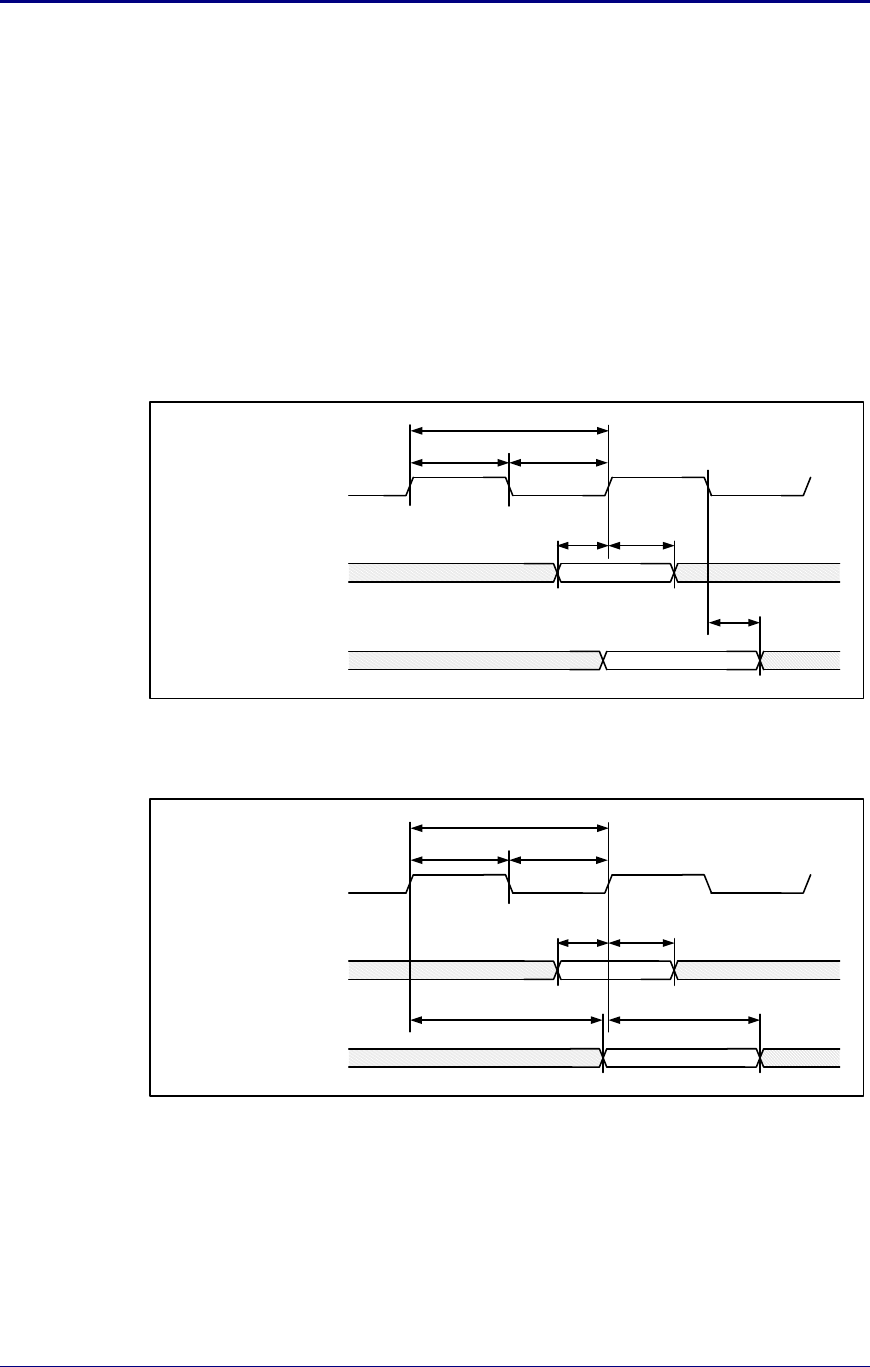
9.0 SDIO Interface
The Serial Data Input Output (SDIO) interface for the WLRG-RA-DP601 is detailed in the
following section. The interface is powered by the VHIO (pin 4 & 6) supply as defined in
Table 2. The interface is compliant to v1.0 of the SDIO interface standard.
9.1 SDIO Protocol Timing
The following figures and table define the required timing for the SDIO interface.
Figure 4 – SDIO Protocol Timing Diagram
SDIO Clock
Data OUT
Data IN
tODLY
fPP
tWL
Data OUT
Data IN
tWH
tISU tIH
Figure 5 – SDIO Protocol Timing Diagram – High Speed
SDIO Clock
Data OUT
Data IN
tOH
fPP
tWL
Data OUT
Data IN
tWH
tODLY
tISU tIH

Product Brief – Airborne SDIO/SPI 802.11b/g Radio Quatech, Inc.
846-8310-240 June 2010 20
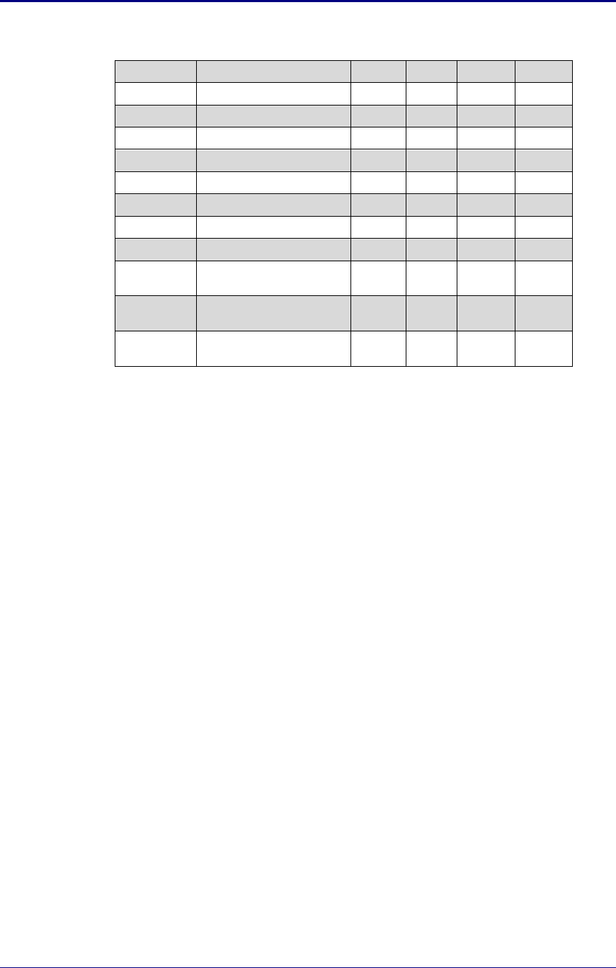
Table 14 - SDIO Protocol Timing Values
Symbol
Parameter
Condition
Min
Typ
Max
Units
fPP
Clock Frequency
Normal
0
25
MHz
High Speed
0
50
MHz
TWL
Clock Low
Normal
10
ns
High Speed
7
ns
TWH
Clock High
Normal
10
ns
High Speed
7
ns
TISU
Input Setup Time
Normal
5
ns
High Speed
6
ns
TIH
Input Hold Time
Normal
5
ns
High Speed
2
ns
TODLY
Output Delay Time
0
14
ns
TOH
Output Hold Time
High Speed
2.5
ns
Product Brief – Airborne SDIO/SPI 802.11b/g Radio Quatech, Inc.
846-8310-240 June 2010 21
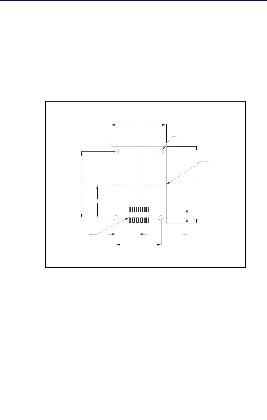
10.0 Mechanical Outline
Figure 6 - Mechanical Outline
29.00mm25.00mm
12.50mm
Molex 53748-0308
BOTTOM VIEW
17.00mm
8.50mm 1.20mm
21.00mm
Ø1.85mm
TOP VIEW
2.50mm
5.87mm
0.80mm
12.00mm
4.50mm
802.11 Antenna Connector
129
230
Radio Connector: 0537480308 (Molex)
(0.50mm (.020") Pitch SlimStack™ Plug, Surface Mount, Dual Row, Vertical,
3.00mm (.118") Stack Height, 30 Circuits)
Board Connector: 0529910308
(0.50mm (.020") Pitch SlimStack™ Receptacle, Surface Mount, Dual Row,
Vertical, 3.00mm (.118") Stack Height, 30 Circuits)
RF Connector: U.FL
(Hirose, Ultra Small Surface Mount Coaxial Connector)
Mounting Screw: M1.6, 0.35mm pitch, 6-8mm length, Stainless Steel
(McMaster-Carr Part# 91800A008)
Mounting Nut: M1.6, 0.35mm Pitch, Hex, Stainless Steel
(McMaster-Carr Part# 91828A006)
Spacer: 3mm, OD 3-4 mm, ID 2–2.5mm
(Bivar Part# 9913-3mm, Nylon 3mm , 2.3mm ID, 4.7mm OD)

Product Brief – Airborne SDIO/SPI 802.11b/g Radio Quatech, Inc.
846-8310-240 June 2010 22
11.0 Design Guidelines
The WLRG-RA-DP601 is designed for integration in to a wide range of advanced
electronic systems and diverse applications, the success of the integration and final
performance of the complete system depends upon the integration process and hardware
design, the following section provides a set of guidelines to aid in the integration of the
radio.
The following guidelines address hardware design requirements for the integration of the
radio under normal conditions, should your application not be able to support the listed
guidelines please contact Quatech.
11.1 VDD/VHIO Power Supply
The WLRG-RA-DP601 supports a split power supply; it requires both a VHIO and
VDD power supply to function correctly.
VHIO defines the power domain that supports the host interface and must be
powered to support the mating interface on the host. It will support both a
1.8VDC and 3.3VDC supply rail.
VDD is the main power supply for the radio and supplies all aspects of the radio
with the exception of the host interface. The VDD is a 3.3VDC supply, please
refer to Table 6 for the power supply requirements.
If the SDIO interface is being used the radio supports the power specification as
defined by the SDIO interface specification, no additional power supply support is
required.
It is acceptable to supply VHIO from the VDD power rail if the host supports a
3.3VDC interface. The full interface specification can be referenced in Table 7.
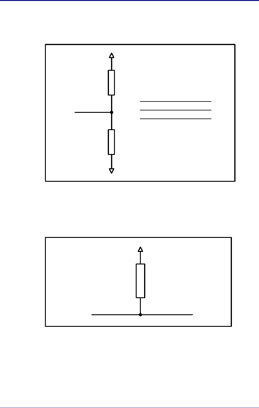
11.2 SDIO (pin #5)
This pin defines the host interface boot definition for the radio, defining either a
SDIO or SPI interface. This pin should be configured as shown in Table 15 for
the radio to boot successfully.
Table 15 - SDIO (Pin #5) Configuration Options
Figure 7 show the recommended network for the pin.
SDIO Mode
Description
SPI
Pin must be pulled to ground.
SDIO
Pin must be pulled to VDD.
Product Brief – Airborne SDIO/SPI 802.11b/g Radio Quatech, Inc.
846-8310-240 June 2010 23
Figure 7 - SDIO (Pin #5) Configuration Options
100K
SDIO
VDD
0
SDIO
R1
SPI
R2
üDNP
R1
R2
ü
DNP
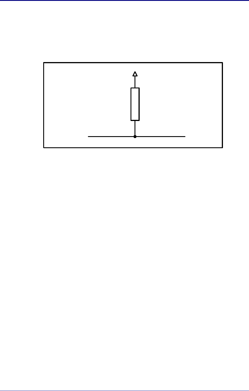
11.3 WLNAPU (pin #16)
This pin should be pulled to VHIO through a 100K resistor, as shown in Fig XX.
Figure 8 - WLNAPU (Pin #16) Network
100K
To HostWLNAPU
VHIO
Product Brief – Airborne SDIO/SPI 802.11b/g Radio Quatech, Inc.
846-8310-240 June 2010 25
11.5 Recommended PCB Layout
The following outlines Quatech‟s recommendations for layout of the PCB for the
WLRG-RA-DP601, these are guidelines only and should serve as guidance when
designing the host system board.
If there are questions relating to the guidelines please contact Quatech Technical
Support.
Figure 10 - Recommended PCB Layout
Board Outline
Molex 52991-0308
Ø1.85mm
17.00mm
1.20mm
29.00mm25.00mm
12.50mm
8.50mm
21.00mm
29
30 2
1
Product Brief – Airborne SDIO/SPI 802.11b/g Radio Quatech, Inc.
846-8310-240 June 2010 26
Figure 11 - Recommended Connector Footprint
1.10mm
2.20mm±0.10mm
30 2
0.25mm±0.05mm
29
0.50mm±0.05mm
1.80mm±0.10mm
1
11.6 Mechanical Mounting
It is recommended that mechanical mounting, other than the mated connector,
be used to secure the radio to the host system. The radio includes four (4) holes
specifically for this purpose. These holes are provides in the four corners and are
unplated, this allows the use of metallic mounting systems without impacting the
electrical performance of the unit.
The mounting holes can be seen in Fig, they are 1.85mm in diameter. A
mechanical spacer will be required to maintain the physical separation of the
board from the host and aid in ensuring optimal interference in the connector.
The height of the spacer should be 3mm±0.1mm. The material should not be
easily compressed.
11.7 EMI/EMF Guidelines
To minimize electromagnetic interference (EMI) and radio frequency interference
(RFI), pay strict attention to power and signal routing near the Radio. As much as
possible, the keep-clear area below the Radio should be a solid copper ground
plane. It is anticipated that the Radio will be mounted on a board with a
committed ground plane. Ensure the PCB interconnect has a designed
impedance of 50-75 Ohms.
To keep signal impedance as low as possible, connect the ground plane to
internal ground planes by several vias. Ground signals to the Radio connector
should connect directly to the ground plane below the Radio. Individual ground
connections to the Radio should have a solid ground connection, preferably
directly to the ground plane on the same surface side where the Radio resides.
Do not connect ground pins directly to an inside layer ground plane using vias
only.

Product Brief – Airborne SDIO/SPI 802.11b/g Radio Quatech, Inc.
846-8310-240 June 2010 27
Keep interconnects from the Radio connector as short as possible on the
mounting layer. All inboard signals–including pin numbers–must immediately
transition to a different routing layer using a via as close to the connector as
possible. Outboard signals (odd pin numbers) should also be kept to a minimum
length.
Product Brief – Airborne SDIO/SPI 802.11b/g Radio Quatech, Inc.
846-8310-240 June 2010 28
12.0 Certification & Regulatory Approvals
The unit complies with the following agency approvals:
Table 16 - Regulatory Approvals
Country
Standard
Status
North America
(US & Canada)
FCC Part 15, Sec. 15.107, 15.109, 15.207, 15.209,
15.247
RSS-210
Modular Approval
Granted
Europe
EN60950 inc. A1, A2, A3, A4
ETSI EN 300 328 Part 1 V1.2.2 (2000-07)
ETSI EN 300 328 Part 2 V1.1.1 (2000-07)
ETSI EN 301 893 V1.2.1 (2002-07)
ETSI EN 301 489-1 V1.4.1 (2002-08)
ETSI EN 301 489-17 V1.4.1 (2000-09)
Pending
Japan
ARIB STD-T71 v1.0, 14 (Dec 2000)
ARIB RCR STD-T33 (June 19, 1997)
ARIB STD-T66 v2.0 (March 28, 2002)
Pending
12.1 FCC Statement
This equipment has been tested and found to comply with the limits for a Class A
digital device, pursuant to Part 15 of the FCC Rules. These limits are designed
to provide reasonable protection against harmful interference in a residential
installation. This equipment generates uses and can radiate radio frequency
energy and if not installed and used in accordance with the instructions, may
cause harmful interference to radio communications. However, there is no
guarantee that interference will not occur in a particular installation. If this
equipment does cause harmful interference to radio or television reception, which
can be determined by turning the equipment off and on, the user is encouraged
to try to correct the interference by one or more of the following measures:
Reorient or relocate the receiving antenna.
Increase the separation between the equipment and receiver.
Connect the equipment to an outlet on a circuit different from that to which
the receiver is connected.
Consult the dealer or an experienced radio/TV technician for assistance.
12.2 SAR Statement
The WLRG-RA-DP601 has been tested for body-worn Specific Absorption Rate
(SAR) compliance. The FCC has established detailed SAR requirements and has
established that these requirements have been met while the WLRG-RA-DP601
was installed in a host representative host system.
Product Brief – Airborne SDIO/SPI 802.11b/g Radio Quatech, Inc.
846-8310-240 June 2010 29
12.3 RF Exposure Information
The radio module has been evaluated under FCC Bulletin OET 65C (01-01) and
found to be compliant to the requirements as set forth in CFR 47 Sections,
2.1093, and 15.247 (b) (4) addressing RF Exposure from radio frequency
devices. This model meets the applicable government requirements for exposure
to radio frequency waves. The highest SAR level measured for this device was
0.993 W/kg (802.11b) and 0.442 W/Kg (802.11g).
For the limited modular approval if the device is used less than 20 cm from
persons (i.e. portable) then the antenna must be mounted outside of the host. If
the device is used more than 20cm from persons (i.e. mobile) then the antenna
does not need to be mounted outside of the host.
Certified antennas include:
Company
Description
Part No.
L-Com
2.2 dBi Omni-directional, 2.4GHz, RP-SMA,
Rubber Duck
HG2402RD-RSF
12.4 Information for Canadian Users (IC Notice)
This device has been designed to operate with an antenna having a maximum
gain of 5dBi for 802.11b/g band. An antenna having a higher gain is strictly
prohibited per regulations of Industry Canada. The required antenna impedance
is 50 ohms.
To reduce potential radio interference to other users, the antenna type and its
gain should be so chosen that the equivalent isotropically radiated power (EIRP)
is not more than required for successful communication.
Operation is subject to the following two conditions: (1) this device may not cause
interference, and (2) this device must accept any interference, including
interference that may cause undesired operation of the device.
12.5 FCC/IOC Limited Modular Approval
This document describes the Airborne WLN FCC limited modular approval and
the guidelines for use as outlined in FCC Public Notice (DA-00-1407A1).
The WLRG-RA-DP601 is covered by the following limited modular grants:
Country
Standard
Grant
North America (US)
FCC Part 15
Sec. 15.107, 15.109, 15.207, 15.209, 15.247
Modular Approval
F4AWLRG601
Canada
RSS 210
Modular Approval
3913A-WLRG601
By providing FCC limited modular approval on the Airborne radio modules, our
customers are relieved of any need to perform FCC part15 subpart C Intentional

Product Brief – Airborne SDIO/SPI 802.11b/g Radio Quatech, Inc.
846-8310-240 June 2010 30
Radiator testing and certification, except where they wish to use an antenna that
is not already certified.
Quatech supports a group of pre-approved antenna; use of one of these
antennas eliminates the need to do any further subpart C testing or certification.
If an antenna is not on the list, it is a simple process to add it to the pre-approved
list without having to complete a full set of emissions testing. Please contact
Quatech Technical support for details of our qualification processes.
Please note that as part of the FCC requirements for the use of the modular
approval, the installation of any antenna must require a professional installer.
This is to prevent any non-authorized antenna being used with the radio. There
are ways to support this requirement but the most popular is to utilize a non-
standard antenna connector, this designation includes the reverse polarity
versions of the most popular RF antenna types (SMA, TNC, etc.). For more
details please contact Quatech.
The following documents are associated with this applications note:
FCC Part 15 – Radio Frequency Devices
FCC Public Notice – DA-00-1407A1 (June 26th, 2000)
Quatech recommends that during the integration of the radio, into the customers
system, that any design guidelines be followed. Please contact Quatech
Technical Support if you have any concerns regarding the hardware integration.
Contact Quatech Technical support for a copy of the FCC and IOC grant
certificates, the test reports and updated approved antenna list.
12.6 Regulatory Test Mode Support
The WLRG-RA-DP601 includes support for all FCC, IC and ETSI test modes
required to perform regulatory compliance testing. Please contact Quatech
Technical Support for details on enabling and using these modes.
Product Brief – Airborne SDIO/SPI 802.11b/g Radio Quatech, Inc.
846-8310-240 June 2010 31
13.0 Change Log
The following table indicates all changes made to this document:
Version
Date
Section
Change Description
Author
A
2/11/2007
-
Internal Release
ACR
B
2/19/2007
4.0
Updated Table 2.0
ACR
1.3
3/12/2008
-
Changed revision numbering from Alpha to Numeric
ACR
2.0
Updated block diagram to remove BT RF connector.
4.0
Updated Table 2.0 to reflect updated pin out.
Updated Connector reference diagram to remove BT connector.
7.0
Updated Fig 2.0 to remove BT U.FL connector.
1.4
3/21/2008
4.0
Updated Table 2.0
ACR
5.0
Updated Table 6.0, 7.0 and 10 with tested values.
Updated notes.
7.0
Updated Fig 2.0 mechanical Outline with new pin #1 identifier.
8.0
Added section
9.0
Added section
1.5
5/8/2008
1.0
Fig 1.0 updated to actual radio image.
ACR
8.0
Fig 3.0 was updated to reflect 10K ohm resistor and modified
population table.
1.6
6/31/2008
7.0
Added Bluetooth Coexistence Interface section.
ACR
9/17/2008
8.0
Added GSPI Section, incremented all sections above.
1.7
11/21/2008
Title
Updated title to include product part number
ACR
4.0
Updated tables 2.0 and 4.0 to correct issues with SPI interface
description.
8.1
Updated Fig 2 & 3 to reflect changes to SPI interface description.
2.0
3/31/09
Title
Removed „Preliminary‟
ACR
5.0
Updated Table 10 with RevB test data.
11.0
Typographical correction
2.1
6/17/2009
5.0
Added Note 2 to Table 5.0
ACR
10.4
Changed Figure reference to identify correct diagram.
11.0
Deleted RESETSection.
2.2
1/31/2010
3.0
Note 1 of Table 1: Correct pin reference from pin 6 to pin 5.
ACR
10.0
Updated mounting hardware reference.
2.3
6/22/2010
12
Updated with FCC/IC regulatory information upon approval.
CHM
2.4
6/28/2010
12
Added SAR certification notice.
Changed FCC/IC approval to limited modular.
ACR