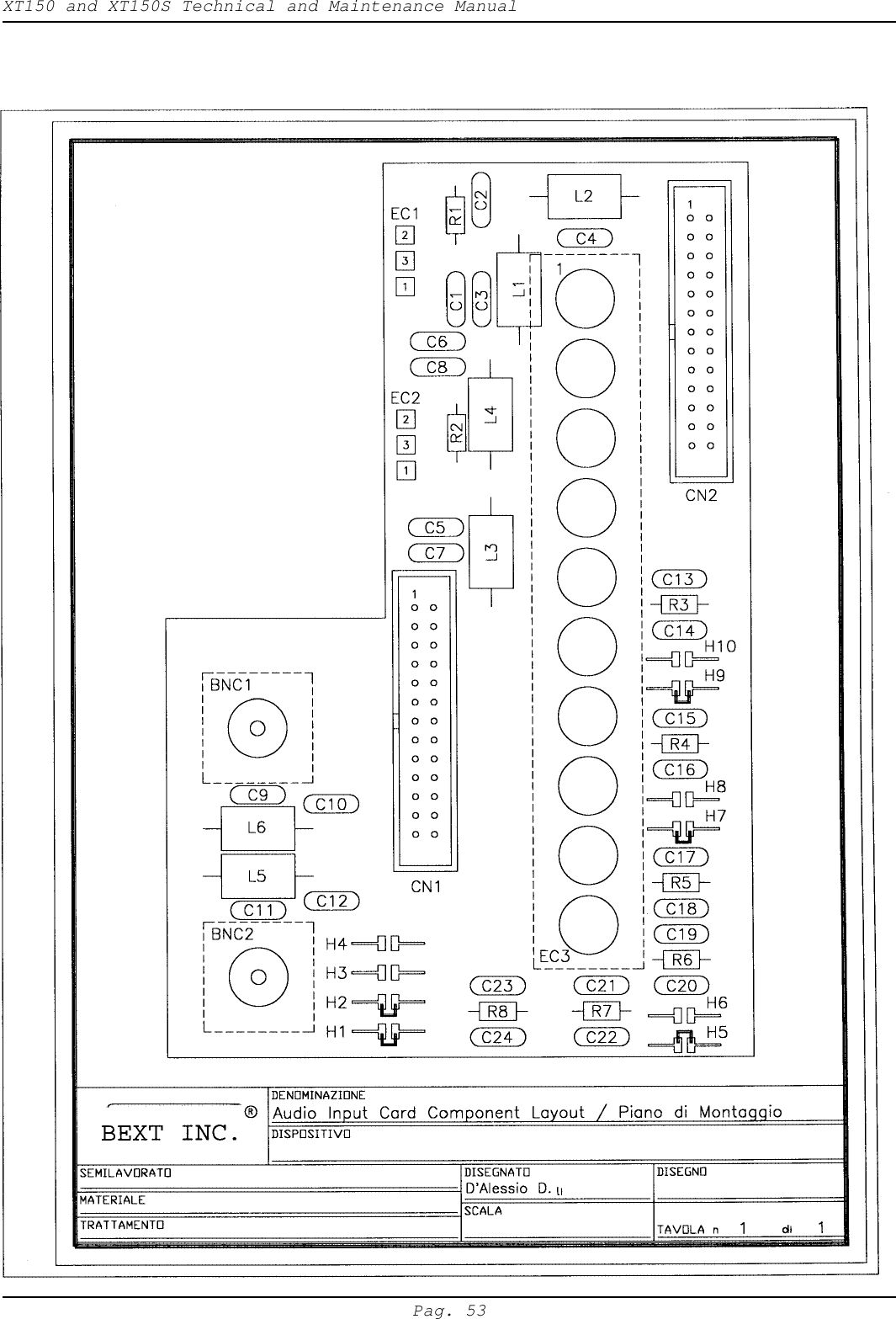
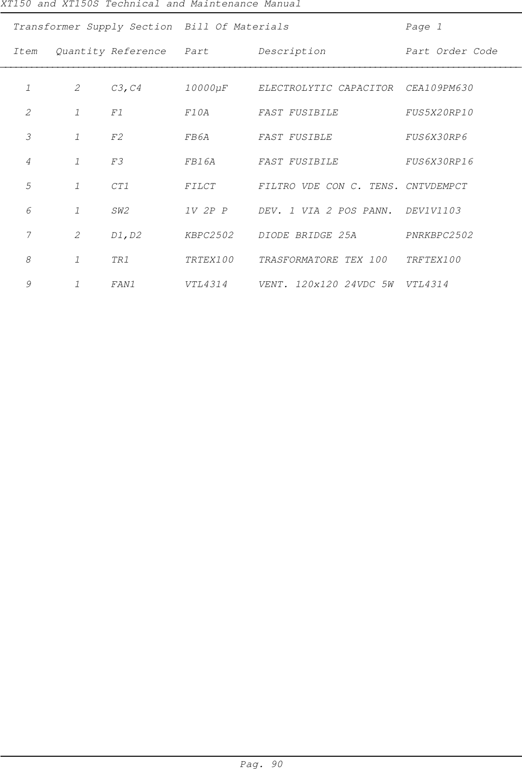
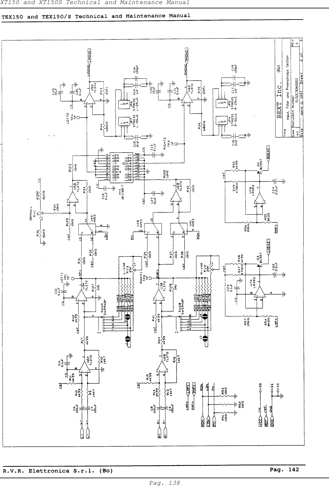
BEXT 072503FMW150 XT 150 Frequency agile FM Transmitter User Manual XT150 150Sa Viewable

BEXT Inc XT 150 Frequency agile FM Transmitter XT150 150Sa Viewable
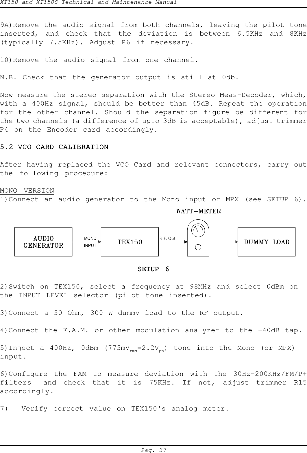
Users Manual

TECHNICAL AND MAINTENANCE MANUALTECHNICAL AND MAINTENANCE MANUALTECHNICAL AND MAINTENANCE MANUALTECHNICAL AND MAINTENANCE MANUALTECHNICAL AND MAINTENANCE MANUALXT 150&XT 150/SBEXT  Inc. - 1045 TENTH AVE. - SAN DIEGO, CA 92101 USA(619) 239-8462 - FAX (619) 239-8474http://www.bext.com - e-mail: support@bext.com
XT150 and XT150S Technical and Maintenance ManualPag. 2INDEXINDEXINDEXINDEXINDEXSECTION 1General Description Pag. 4Electrical Specifications (Table A) Pag. 6Dimensional & Environmental Specifications (Table B) Pag. 8SECTION 2Electrical Description Pag. 9Front Panel's View Description (Stereo Version) Pag. 12Front Panel's View (Fig. 1A) Pag. 14Front Panel's View Description (Mono Version) Pag. 13Front Panel's View (Fig. 1B) Pag. 15Rear Panel's View Description Pag. 16Rear Panel's View (Fig. 2) Pag. 17Block Diagram (Fig. 3) Pag. 18Top's View Description Pag. 19Top's View (Fig. 4) Pag. 20Down's View Description Pag. 21Upper's View (Fig. 5) Pag. 22Recommend Test Equipment (Table C) Pag. 23SECTION 3Installation Procedures Pag. 24SECTION 4Maintenance Procedures Pag. 29SECTION 5Calibration Procedure of Modules Pag. 36APPENDIX ACircuit Diagram, Bills of Material and Layouts Pag. 46Wiring Diagrams Pag. 47Audio Input Card Pag. 50Frequency Selector Card (Mod. TSW-1) Pag. 54
XT150 and XT150S Technical and Maintenance ManualPag. 3Frequency Selector Card (Mod. TSW-3) Pag. 58VCO Card Pag. 62PLL Card Pag. 70Alarms Card Pag. 78Meter Card Pag. 83Transformer Supply Section Pag. 88Main Power Supply Pag. 91Switching 1 Power Supply Pag. 95Switching 2 Power Supply Pag. 99Mono/MPX Card Pag. 103Stereo Coder Card (Mod. SDC30) Pag. 109R.F. Power Amplifier Pag. 116Low Pass Filter Card Pag. 120Directional Coupler Card Pag. 124Clipper Card Pag. 128150PS2 Card Pag. 132Stereo Coder Card (Mod. SDC30A002) Pag. 136TCXO Card Pag. 151
XT150 and XT150S Technical and Maintenance ManualPag. 4CHAPTER 1GENERAL DESCRIPTIONGENERAL DESCRIPTIONGENERAL DESCRIPTIONGENERAL DESCRIPTIONGENERAL DESCRIPTION1.0 INTRODUCTION1.0 INTRODUCTION1.0 INTRODUCTION1.0 INTRODUCTION1.0 INTRODUCTIONThis manual gives necessary information about XT150 and XT150S exciter. Whenreferring to the Mono or Stereo Version, it will be duly noted.1.1 GENERAL DESCRIPTION1.1 GENERAL DESCRIPTION1.1 GENERAL DESCRIPTION1.1 GENERAL DESCRIPTION1.1 GENERAL DESCRIPTIONThe XT150 is housed in a 3U, 19" rack-mouting container comprising a number ofinterconnected modules mounted internally on the main chassis, facilitatingremoval and  substitution.The power output control, audio input level controland analog meter for the measurement of operating parameters, are all mountedon the front panel.The line power, audio input, RF output and telemetry (optional) connectors aremounted on the rear panel.1.2  ELECTRICAL DESCRIPTION1.2  ELECTRICAL DESCRIPTION1.2  ELECTRICAL DESCRIPTION1.2  ELECTRICAL DESCRIPTION1.2  ELECTRICAL DESCRIPTIONThe XT150 is an exciter working in the 87.5 to 108 MHz band, programmable insteps of 10KHz. Its power output is continuously adjustable from 10W to 150Winto a 50 Ohm load.The XT150 incorporates a stereo coder which guarantees excellent stereoseparation together with low harmonic distortion (only for Stereo version). Italso accepts two SCA signals. A front panel switch allows stereo operation (onlyfor stereo version) or "mono/mpx" operation which excludes the stereo encoderand uses the "right" input as the mono input and the "left" input as the widebandcomposite input. The specification features low audio distortion andintermodulation figures (typically 0.03%) and a high signal-to-noise ratio(typically -80 dB). A voltage selector on the transformer primary allows a varietyof supply voltages to be used.1.3 METERS AND INDICATORS1.3 METERS AND INDICATORS1.3 METERS AND INDICATORS1.3 METERS AND INDICATORS1.3 METERS AND INDICATORSThe operating parameters of the exciter can be monitored using the analogmultimeter (12 Fig.1A and 8 Fig.1B) situated on the front panel. The parameterto be measured is selected by the rotary selector (11 Fig.1A and 7 Fig.1B). Thefrequency control (10 Fig.1A and 14 FIg.1B) allows frequencies to be selectedin steps of 10KHz. Three red alarm leds indicate VCO unlock (15 Fig.1A and 11Fig.1B), excess VSWR on the output and the excess of temperature (4 Fig.1A and8 Fig.1B), and the shutdown condition, programmed by a remote command (10 Fig.1Aand 6 Fig.1B). Three green leds (7 Fig.1A and 3 Fig.1B) indicate the presenceof +12V, +15V and +28V voltages which are used to power the various cards insidethe exciter. A selector (2 Fig.1A) allows selection between Mono/MPX and Stereofunctions and another selector (6 Fig.1A and 2 Fig.1B) is provided to choosethe level of the input signal. Trimmers are provided for adjustment of left andright channels (5 Fig.1A and 1 Fig.1B) and a switch allows the stereo subcarrierto benabled or disabled (3 Fig.1A).1.4 AUTOMATIC FREQUENCY CONTROL1.4 AUTOMATIC FREQUENCY CONTROL1.4 AUTOMATIC FREQUENCY CONTROL1.4 AUTOMATIC FREQUENCY CONTROL1.4 AUTOMATIC FREQUENCY CONTROLThe operating frequency is governed by a thermally-compensated, reference
XT150 and XT150S Technical and Maintenance ManualPag. 5oscillator working within a phase-locked loop (PLL). The XT150 reaches frequencylock within a maximum of 30 seconds.1.5 CONTROL CIRCUITS1.5 CONTROL CIRCUITS1.5 CONTROL CIRCUITS1.5 CONTROL CIRCUITS1.5 CONTROL CIRCUITSThe control circuits allow automatic control of output power(internal andexternal), maintaining the chosen power level across the entire operating band.Furthermore another circuit protects the final stage against excessive VSWR orshort circuits and excessive temperature. Then, there are other protectioncircuits that allow to limit the maximum output power and to protect the equipmentagainst a power supply's overvoltage.1.6 R.F. AMPLIFIER1.6 R.F. AMPLIFIER1.6 R.F. AMPLIFIER1.6 R.F. AMPLIFIER1.6 R.F. AMPLIFIERThe RF amplifier is a wide-band design and guarantees an adjustable power outputof 10 to 150 watts across the entire band. A low-pass filter enables the TEX150to be used as a low power transmitter, connected directly to an antenna.1.7 TECHNICAL SPECIFICATIONS1.7 TECHNICAL SPECIFICATIONS1.7 TECHNICAL SPECIFICATIONS1.7 TECHNICAL SPECIFICATIONS1.7 TECHNICAL SPECIFICATIONSPlease refer to Table (A) for the electrical specifications and Table (B) forthe mechanical specifications.
XT150 and XT150S Technical and Maintenance ManualPag. 6TABLE AELECTRICAL SPECIFICATIONSELECTRICAL SPECIFICATIONSELECTRICAL SPECIFICATIONSELECTRICAL SPECIFICATIONSELECTRICAL SPECIFICATIONSPower Supply 100-130V, 50-60Hz198-250V, 50-60HzPower Consumption approx. 350WCooling Forced ventilationFrequency Range from 87.5 to 108MHz in stepsof 10KHzOutput Power adjustable from 10 to 100 WAutomatic Output Level Control Stabilizes the set RF outputlevelOutput Impedance 50 OhmOutput Connector Standard "N-type"Harmonic Suppression > -65dBSpurious Signal Suppression > -80dBMono  Intermodulation  Distortion 0.05 % or less, measured at1KHz and 1.3 KHz, ratio 1:1 at100% modulationFrequency  Stability ±500Hz (typ. ±300Hz) from 0°to 50°CModulation Type Direct frequency modulation ofthe RF oscillator atfundamental frequencyFrequency Deviation ±75KHz nominalHarmonic  Distortion < 0.05% (typically 0.01%)FM Signal-to-Noise Ratio > 75 dB mono, > 70 dB stereomeasured with 75KHz deviationin the 30Hz to 15KHz band RMS.Residual AM (Asynchronous) approx. 0.05%=65dB RMSResidual AM (Synchronous) 0.1%=60dBPre-emphasis 50µs ±2% or 75µs ±2%selectable
XT150 and XT150S Technical and Maintenance ManualPag. 7Audio Input Impedance 10KOhm balanced or 5Kohmunbalanced (600ohm on request)Audio Input Level Selectable from -9 to +6 dBmin five steps continuoslyfrom -12 to +9 dBmAudio Frequency Range 30-15000Hz, MONO input30-100000Hz, MPX inputAudio Input Filter > 45dB at 19KHz (Mono)> 40dB from 20KHz to 100KHzMono Frequency Response ±0.3dB from 30Hz to 15KHzMPX Frequency Response ±0.5dB from 30Hz to 75KHzStereo Separation > 45dB (typ. 50dB)Pilot Tone Frequency 19KHz ± 1HzPilot tone level -20dBm adjustableNumber of SCA inputs 2SCA input impedance 1KOhm unbalancedSCA input level 0dBm per ± 7.5KHz of deviationSCA input response ± 0.5dBm from 40KHz to 100KHz
XT150 and XT150S Technical and Maintenance ManualPag. 8TABLE BMECHANICAL SPECIFICATIONSMECHANICAL SPECIFICATIONSMECHANICAL SPECIFICATIONSMECHANICAL SPECIFICATIONSMECHANICAL SPECIFICATIONSRack dimensions 483.00 mm (19.0") W132.50 mm (5.20") H345.00 mm (13.7") DOperating temperature from -10°C to 50°CHumidity 95% max., non-condensingWeight 12 Kg
XT150 and XT150S Technical and Maintenance ManualPag. 9CHAPTER 2ELECTRICAL DESCRIPTIONELECTRICAL DESCRIPTIONELECTRICAL DESCRIPTIONELECTRICAL DESCRIPTIONELECTRICAL DESCRIPTION2.1 INTRODUCTION2.1 INTRODUCTION2.1 INTRODUCTION2.1 INTRODUCTION2.1 INTRODUCTIONThis section describes, in detail, the operating theory behind theXT150. To  aid understanding, the unit has been subdivided intoblocks, each of which is fully described below. The block diagramis shown in Fig.3.2.2 POWER SUPPLY2.2 POWER SUPPLY2.2 POWER SUPPLY2.2 POWER SUPPLY2.2 POWER SUPPLYThis circuit comprises a board, mounted on a heat sink, which is fixedto the central part of the lower section of the unit (2 Fig.5). The powersupply generates the various stabilized voltages necessary for each ofthe various modules that make up the XT150. The transformer has aselectable input from 110 V to 240 V and two outputs A +18V (6.3A) andB +32V (10A). This power supply is composed of two main parts: afterhaving undergone filtering for mains-borne interference, the supply istransformed into four lower voltages, rectified, smoothed andstabilized to the following values: +12V, +15V and 10 to 28V variableto obtain the high efficiency (85-90%). The +15V supplies the encodermixer, the PLL card, the VCO card, the meter 100 card and the alarm card.The +12V supplies the input of RF power amplifier driver (BGY33) andthe 10-28V variable supplies the output of RF power amplifier driver(BGY33) and the final power stage of the same module (two MRF317 or twoSD1480).The variable voltage of the final stage is controlled by the PWR ADJcontrol which determines the R.F. power output of the exciter. Theautomatic control of output power guarantees the power level set by thePWR ADJ control right across the frequency range and independantly ofother variables such as temperature, load variations etc. The systemworks by comparing the value set by the PWR ADJ control with the actualpower output of the unit and compensating accordingly. The final stagedriveris composed of two separate parts, the input part is supplied with+12V voltage, and the output part is supplied by the switching  powersupply with 4-12V variable voltage obtained dividing the 10-28Vvariable voltage. A power limiting circuit intervenes in the eventof excess SWR on the output, thus protecting the final stage.2.3 AUDIO INPUT CARD2.3 AUDIO INPUT CARD2.3 AUDIO INPUT CARD2.3 AUDIO INPUT CARD2.3 AUDIO INPUT CARDThis card is situated on the rear panel of the exciter (1 Fig.4 and 3Fig.5). The card filters all audio signal inputs to the unit, removingRF interference, before supplying them to the encoder mixer or Mono\MPXcard. The main operating parameters of the exciter are available forremote monitoring via a telemetry connector.
XT150 and XT150S Technical and Maintenance ManualPag. 102.4 CODER MIXER (only for Stereo Version)2.4 CODER MIXER (only for Stereo Version)2.4 CODER MIXER (only for Stereo Version)2.4 CODER MIXER (only for Stereo Version)2.4 CODER MIXER (only for Stereo Version)This card is situated in the lower part of the unit (6 Fig.4).The card can function either as a stereo encoder or as a simple mixerfor the various audio inputs. The function may be selected by acontrol situated on the front panel. In stereo encoder mode, the 19KHzpilot tone is derived from a quartz crystal reference oscillator. Sotoo is the samplingfrequency which allows the L and R signals to be separated from themultiplexed signal, plus the suppression of the 38KHz frequency. Thelevel of the left and right signals is set by the corresponding selectorsituated on the front panel. The signals are then filtered at 15KHz andpre-emphasized (50µS CCIR, 75µS FCC) before being sent to the multiplexcircuit. The audio signals from the two SCA inputs are mixed in to providethe output. In mixer mode (Mono MPX) the stereo encoder is bypassed,the right input accepts a mono signal and the left input accepts amultiplex signal upto 100KHz. The SCA inputs remain unchanged. Threerectifiers allow the peak levels of the two inputs "Left/MPX" and "right/mono" to be displayed on the analog meter, and provide the audio detectorcircuit with the deviation level.2.5 PLL CARD2.5 PLL CARD2.5 PLL CARD2.5 PLL CARD2.5 PLL CARDThe PLL card is situated internally, in the upper part of the unit (6 Fig.5). The circuit includes a reference cristal oscillator (optionalhigh stability), a logic section that includes the frequncy dividersand comparator. The reference cristal oscillator generates a 4MHzfrequency that is divided to generate a 1KHz fixed signal. This signalis  compared to the operating frequency generated by the VCO  dividedopportunely  on the ground of the frequency setted on the Contraves. Anindicator  situated on the front panel signals the "unlocked" condition.The comparator output (AFC signal) is sent to the varicap diodes situatedon the VCO Card.2.6 VCO CARD2.6 VCO CARD2.6 VCO CARD2.6 VCO CARD2.6 VCO CARDThe VCO card is situated internally, in the upper part of the unit(4 Fig.4). This module includes an audio input stage at low frequency,a voltage controlled oscillator at low noise (VCO) and a driver stage.The audio signal supplied by the encoder mixer is amplified and theninjected into the VCO to provide class F3 modulation. The voltagecontrolled oscillator (VCO) generates the signal on the frequency settedon the Contraves. This signal is amplified to 300 mW level (25dBm) todrive the final stage and to be sent to PLL circuit situated on the PLLcard. The operating frequency genereted by the VCO is divided down before
XT150 and XT150S Technical and Maintenance ManualPag. 11being compared to a reference frequency, generated by a high stabilityoscillator (standard 5ppm). The error voltage is filtered and used tocompensate the VCO frequency and guarantee its stability. A trimmer ispresent on this card for adjustment of deviation.2.7 R.F. POWER AMPLIFIER2.7 R.F. POWER AMPLIFIER2.7 R.F. POWER AMPLIFIER2.7 R.F. POWER AMPLIFIER2.7 R.F. POWER AMPLIFIERThe final power stage is mounted on a heat sink to dissapate waste heatand is enclosed in a totally screened, metal container, fixed to theupper-middle part of the central section of the unit (1 Fig.5). The RFsignal coming from the Stereo Decoder or Mono\MPX at a power level ofabout 300 mW, reaches the driver stage (BGY33) and is amplified to alevel from about 1W to 20 W before being further amplified by the finalstage (two MRF317 or two SD1480) to a level of upto 150 W. The resultantsignal is then filtered by a low-pass filter (2 Fig.5) which removesany harmonic content.A  directional coupler allows the direct andreflected power levels to be measured and displayed on the analogmultimeter and also fedback to the power supply for automatic controlof the output power (see Power Supply description). A BNC connectorsituated on the rear panel provides a power signal at -40 dB of theamplifier output power.2.8 METER  CARD2.8 METER  CARD2.8 METER  CARD2.8 METER  CARD2.8 METER  CARDThis card is situated centrally on the front panel (5 Fig.4 and 7 Fig.5).The card receives direct and reflected power signals from the powersupply which, in turn, come from the final power stage. The Stereoencoder card supplies deviation and left and right signal levels.These  signal  levelsare then displayed on the analog meter according tothe position of therotary selector situated on the front panel.2.9 CONTRAVES  CARD2.9 CONTRAVES  CARD2.9 CONTRAVES  CARD2.9 CONTRAVES  CARD2.9 CONTRAVES  CARDThis card is fixed to the left-hand side of the front panel (5 Fig.5).The operating frequency selected by the frequency control is representedby a signal which is supplied to the frequency dividers that form partof the PLL circuits found on the PLL card.2.10 ALARMS  CARD2.10 ALARMS  CARD2.10 ALARMS  CARD2.10 ALARMS  CARD2.10 ALARMS  CARDThis card is fixed in the lower part of the unit (7 Fig.4). This circuitallows to adjust, through 7 trimmers, the threeshold of the  externaland internal output level, internal and external VSWR level, temperatureand to preset the maximum value of the output power. In case of faultthere isn't an automatic reset, because the transmitter provides todecrease the output power to continue the transmission withoutstops,even if at minimum power.
XT150 and XT150S Technical and Maintenance ManualPag. 122.11 MONO\MPX CODER CARD (Mono  Version)2.11 MONO\MPX CODER CARD (Mono  Version)2.11 MONO\MPX CODER CARD (Mono  Version)2.11 MONO\MPX CODER CARD (Mono  Version)2.11 MONO\MPX CODER CARD (Mono  Version)This card is fixed in the lower part of the unit. The Mono\MPX card isan Audio Mixer at four inputs, two balanced (Mono and MPX) and twounbalanced (SCA1 and SCA2). Mono and MPX input level can be settedthrough relative switches placed on front panel, on 5 fixed positionsand on a variable position from -12dBm to +9dBm (pre-setted at 0dBm).It's possible to set the pre-enphasis value at 50µS, 75µS or linear.Then, it's possible to insert or remove a low pass filter at 15KHz.2.12 CLIPPER CARD (Optional)2.12 CLIPPER CARD (Optional)2.12 CLIPPER CARD (Optional)2.12 CLIPPER CARD (Optional)2.12 CLIPPER CARD (Optional)This card is fixed with a sandwich structure on the coder card and isaccesible from lower part of the equipment. Its function is thatto limit drastically any audio signal that exceeds a prefixedthreshold. Therefore, it's used to avoid any type of over-modulationas to maximum peak permitted of ± 75KHz. With an exceeding signal,immediately too, of 6 dB the nominallevel for a deviation of ± 75KHz, this card allows to contain deviationincreasing within 1dB.FRONT PANEL STEREO VERSION VIEW DESCRIPTION (FIG.1A)FRONT PANEL STEREO VERSION VIEW DESCRIPTION (FIG.1A)FRONT PANEL STEREO VERSION VIEW DESCRIPTION (FIG.1A)FRONT PANEL STEREO VERSION VIEW DESCRIPTION (FIG.1A)FRONT PANEL STEREO VERSION VIEW DESCRIPTION (FIG.1A)1 STEREO/MONO-MPX Selects STEREO or MONO/MPX operation2 STEREO LED Indicates the operation of the stereo encoder3 19KHz LED Indicates the 19KHz pilot tone presence4 MODE SELECTOR Button in: STEREO OPERATION MODE pilot tonepresentButton out: MONO OPERATION MODE pilot toneabsent5 L/MPX & R/MONO LEVEL L/MPX and R/Mono input level adjustable from-12 to +9 dBm; this is possible if the inputlevel switch is completely turned clockwise6 INPUT LEVEL Input signal attenuator adjustable in5 steps from -9 to +6 dBm7 VOLTAGES LEDS Indicates the presence of the internaloperating voltages +12V, +15V and +28V8 SWR Indicates that reflected power exceeds 10W9 PWR ADJ 10-turn trimmer to regulate the power outputof the exciter. AGC maintains the level set bythis control10 REMOMTE Indicates that the exciter has been shut-downby remote control
XT150 and XT150S Technical and Maintenance ManualPag. 1311 MEASUREMENT SELECTOR The measurement made by the meter correspondsto the position of this selector12 METER Analog meter used to display the followingoperating parameters of the exciter:Direct power f.s. 200WReflected power f.s. 50WDeviation f.s. 100KHzRight channel input level f.s. +3dBLeft channel input level f.s. +3dB13 POWER ON/OFF switch14 MHz/KHz Rotary frequency selector15 L.O. UNLOCK If ON indicates that the VCO is not locked tothe reference frequency. The output power willdrop to zero in this conditionFRONT PANEL MONO VERSION VIEW DESCRIPTION (FIG.1B)FRONT PANEL MONO VERSION VIEW DESCRIPTION (FIG.1B)FRONT PANEL MONO VERSION VIEW DESCRIPTION (FIG.1B)FRONT PANEL MONO VERSION VIEW DESCRIPTION (FIG.1B)FRONT PANEL MONO VERSION VIEW DESCRIPTION (FIG.1B)1 L/MPX & R/MONO LEVEL L/MPX and R/Mono input level adjustable from-12 to +9 dBm2 INPUT LEVEL Input signal attenuator adjustable in 5 stepsfrom -9 to +6 dBm3 VOLTAGES LEDS Indicates the presence of the internaloperating voltages +12V, +15V and +28V4 SWR Indicates that reflected power exceeds 10W5 PWR ADJ 10-turn trimmer to regulate the power outputof the exciter. AGC maintains the level set bythis control6 REMOTE Indicates that the exciter has been shut-downby remote control7 MEASUREMENT SELECTOR The measurement made by the meter correspondsto the position of this selector8 METER Analog meter used to display the followingoperating parameters of the exciter:Direct power f.s. 200WReflected power f.s. 50WDeviation f.s. 100KHzRight channel input level f.s. 3dBLeft channel input level f.s. 3dB9 POWER Supply on/off switch10 MHz/KHz Rotary frequency selector11 L.O. UNLOCK Indicates that the VCO is not locked to thereference frequency. The output power willdrop to zero in this condition
XT150 and XT150S Technical and Maintenance ManualPag. 14FIG. 1A
XT150 and XT150S Technical and Maintenance ManualPag. 15FIG. 1BFIG. 1BFIG. 1BFIG. 1BFIG. 1B
XT150 and XT150S Technical and Maintenance ManualPag. 16REAR PANEL VIEW DESCRIPTIONREAR PANEL VIEW DESCRIPTIONREAR PANEL VIEW DESCRIPTIONREAR PANEL VIEW DESCRIPTIONREAR PANEL VIEW DESCRIPTION(FIG. 2)(FIG. 2)(FIG. 2)(FIG. 2)(FIG. 2)1 FUSE BLOCK Fuse block and line voltage selector. Use asmall screwdriver to change the fuse or theline voltage. Rotate the block and position itfor the desired voltage.2 PLUG Line power connector3 REMOTE 1 BNC connector, External AGC input4 REMOTE 2 BNC connector, External Reflected Feedbackinput5 EXT REF 1 KHz External 1 KHz reference (optional)6 REMOTE 3 BNC connector. Connecting the centralconductor to ground will cause the RF outputpower level to drop to zero and to stay thereuntil the short is removed. When used with anR.V.R. amplifier, this connector should beconnected to the "REMOTE" output of the poweramplifier.7 FAN Fan-assisted cooling for the power stage andthe power supply.8 TELEMETRY TERMINALS 10-pin telemetry card1-2-3-10 GND4 Forward power5 Reflected power6 VPA7 IPA8 SWR alarm9 Unlock alarm9 P.A. FUSE Power Amplifier Protection fuse 8A10 R.F. OUTPUT N-type connector, 50 Ohm11 R.F. TEST POINT -40 dB output referred to the output powerlevel12 FUSE Main Protection Fuse 6A13 RIGHT (MONO) BNC connector for FCC unbalanced version;Cannon XLR for CCIR version with balancedinput14 LEFT (MPX) BNC connector for FCC version; Cannon XLR forCCIR version with balanced input15 SCA 1 BNC connector, unbalanced SCA1 input16 SCA 2 BNC connector, unbalanced SCA2 input or output(internally selactable) for pilot tone (i.e.for RDS encoder)
XT150 and XT150S Technical and Maintenance ManualPag. 17FIG. 2FIG. 2FIG. 2FIG. 2FIG. 2
XT150 and XT150S Technical and Maintenance ManualPag. 18MONO VERSION BLOCK DIAGRAM (FIG.3A)MONO VERSION BLOCK DIAGRAM (FIG.3A)MONO VERSION BLOCK DIAGRAM (FIG.3A)MONO VERSION BLOCK DIAGRAM (FIG.3A)MONO VERSION BLOCK DIAGRAM (FIG.3A)STEREO VERSION BLOCK DIAGRAM (FIG.3B)STEREO VERSION BLOCK DIAGRAM (FIG.3B)STEREO VERSION BLOCK DIAGRAM (FIG.3B)STEREO VERSION BLOCK DIAGRAM (FIG.3B)STEREO VERSION BLOCK DIAGRAM (FIG.3B)
XT150 and XT150S Technical and Maintenance ManualPag. 19TOP VIEW DESCRIPTION (FIG.4)TOP VIEW DESCRIPTION (FIG.4)TOP VIEW DESCRIPTION (FIG.4)TOP VIEW DESCRIPTION (FIG.4)TOP VIEW DESCRIPTION (FIG.4)1 .................... Audio Input Card2 .................... Power Supply Card3 .................... Switch Power Supply 14 .................... Anolog Meter5 .................... Meter Card6 .................... Stereo Coder Card (for Stereo Version)Mono\MPX Card (for Mono Version)7 .................... Alarms Card8 .................... Analog Meter
XT150 and XT150S Technical and Maintenance ManualPag. 20FIG.4FIG.4FIG.4FIG.4FIG.4     1 7 6 5     8 3 2 4
XT150 and XT150S Technical and Maintenance ManualPag. 21DOWN VIEW DESCRIPTION (FIG.5)DOWN VIEW DESCRIPTION (FIG.5)DOWN VIEW DESCRIPTION (FIG.5)DOWN VIEW DESCRIPTION (FIG.5)DOWN VIEW DESCRIPTION (FIG.5)1 .................... Power Amplifier Card2 .................... Low Pass Filter3 .................... Audio Input Card4 .................... VCO Card5 .................... Frequency Selector Card6 .................... PLL Card7 .................... Meter Card8 .................... Switching Power Supply 29 .................... Toroidal transformer10 .................... Directional Coupler
XT150 and XT150S Technical and Maintenance ManualPag. 22FIG. 5FIG. 5FIG. 5FIG. 5FIG. 510289736 145
XT150 and XT150S Technical and Maintenance ManualPag. 23TABLE CRECOMMENDED TEST EQUIPMENTRECOMMENDED TEST EQUIPMENTRECOMMENDED TEST EQUIPMENTRECOMMENDED TEST EQUIPMENTRECOMMENDED TEST EQUIPMENTINSTRUMENTINSTRUMENTINSTRUMENTINSTRUMENTINSTRUMENT MODELMODELMODELMODELMODEL SPECIFICATIONSPECIFICATIONSPECIFICATIONSPECIFICATIONSPECIFICATIONCoaxial Load Resistor Bird Power Rating 300W continuousMod. 8173Wattmeter Bird Power Range: 100mW to 10KWMod. 43 using Bird Plug-in-ElementsFrequency Range: 0.45 to2300MHzPlug-in-Elements Bird Power Rating: 250WFreq. Range: 50 to 125MHzStereo Decoder A.E.V. Stereo Separation: > 60 dBMod. SMD from 30Hz to 15 KHzLow Distorsion Krohn-Hite THD < 0.001%A.F. Generator Mod. 4400AOscilloscope Tektronix 100MHz OscilloscopeMod. 2247A Counter/TimerF.M. Modulation Meter Rohde SchwarzMod. F.A.M.Digital Multimeter Metrix
XT150 and XT150S Technical and Maintenance ManualPag. 24CHAPTER 3INSTALLATION PROCEDURESINSTALLATION PROCEDURESINSTALLATION PROCEDURESINSTALLATION PROCEDURESINSTALLATION PROCEDURES3.1 INTRODUCTION3.1 INTRODUCTION3.1 INTRODUCTION3.1 INTRODUCTION3.1 INTRODUCTIONThis chapter contains the information required for installation of theTEX150 exciter and for preliminary checks.3.2 UNPACKING3.2 UNPACKING3.2 UNPACKING3.2 UNPACKING3.2 UNPACKINGRemove the unit from its packaging and before any other operation, checkfor any damage that the unit may have suffered in transit and that allfront and rear panel controls are functioning.3.3 INSTALLATION3.3 INSTALLATION3.3 INSTALLATION3.3 INSTALLATION3.3 INSTALLATION1)Check that the line voltage selector is correctly set for the localsupply. If not, remove the cover on which the voltages are printedand rotate it until the required value corresponds to the arrow,and reinsert it. Check also that the fuse (1 Fig.2) mounted inside thecover is present and in order.The current capacity of the fuse are as follows:                        220-240 V   -    6.3 A100-120 V   -    12 A2)Now ensure that the PWR ADJ control (9 Fig.1A or 5 Fig.1B) is rotatedfully anti-clockwise, using a small screwdriver. N.B. The control isa ten-turn potentiometer so care should be taken to verify the minimumposition.Units are usually shipped with this control already at minimum.WARNING: When the unit is switched on with the control at its minimumposition, power output is about 10W.3)Connect a dummy load with a power rating of at least 150 W continuousto the RF output, situated on the rear panel of the unit. It is advisableto connect a bypass wattmeter in series with this load in order to verifythe accuracy of the unit's own internal wattmeter (see SETUP 1).SETUP 1SETUP 1SETUP 1SETUP 1SETUP 1XT150 DUMMY LOAD
XT150 and XT150S Technical and Maintenance ManualPag. 254)Connect a switch, via a cable, to the REMOTE 3 connector (4 Fig.2)on the rear panel so that the switch is able to short the centralconductor to its screen. Leave the switch in the short-circuit position.5)Switch the unit's ON/OFF switch (13 Fig.1A or 9 Fig.1B) to the OFFposition.6) Connect line power to the unit via the VDE socket (2 Fig.2).Note: It's essential that the unit be properly earthed to ensure boththe safety of the operator as well as the correct functioning of theequipment.7)Switch the power On switch (13 Fig.1A or 9 Fig.1B) to the ON positionand check that the three green internal voltage led (7 Fig.1A or 3 Fig.1B)and the red UNLOCK led (15 Fig.1A or 11 Fig.1B) are all on. Select thedesired operating frequency using the corresponding selector. The redUNLOCK led should switch off within 30 seconds, indicating that theoscillator has locked onto the operating  frequency. The frequency se-lector comprises five figures of which the three to the left of thedecimal point represent (from left to  right) hundreds of MHz, tens ofMHz and MHz. The two figures to the right of the decimal point  rep-resent (from left to right) hundreds of KHz and tens of KHz.Eg: 098.45 = ninety eight megahertz and four hundred and fiftyKilohertz.Eg: 103.94  = one hundred and three Megahertz and nine hundred and fortyKilohertz.Furthermore, if a frequency is selected beyond the two limits of the87.5-108 MHz band, the amplifier will continue to work even through thedisplayed frequency no longer corresponds to the operating frequencyof the unit.Note: Transmitting outside the legal band (87.5-108 MHz) is an offenceNote: Transmitting outside the legal band (87.5-108 MHz) is an offenceNote: Transmitting outside the legal band (87.5-108 MHz) is an offenceNote: Transmitting outside the legal band (87.5-108 MHz) is an offenceNote: Transmitting outside the legal band (87.5-108 MHz) is an offenceand may lead to prosecution.and may lead to prosecution.and may lead to prosecution.and may lead to prosecution.and may lead to prosecution.8)After having verified that the UNLOCK led is switched off and thatthe unit is therefore locked to the selected operating frequency, switchthe switch connected to the REMOTE connector so as to remove the shortcircuit between the central conductor and ground. The RF output is nowenabled and should correspond to a power level of about 10W. To checkthis reading, select FWD on the meter selector and read the power fromthe 200 W FSD scale.9)Using a small screwdriver, rotate the PWR ADJ control clockwise; thepower output should increase progressively to a maximum of 100W.Check the value with the bypass wattmeter which should be within ±10%.
XT150 and XT150S Technical and Maintenance ManualPag. 2610)With the power output at 150W, select a new operating frequency wellaway from the current value. Eg: 107 MHz: the UNLOCK led should switchon and the power output should fall to zero at the same time. Only whenthe UNLOCK led switches off (unit locked to new frequency) should thepower output resume its previous level.11) Automatic power control checkIt is advisable to start this procedure with the operating frequencyset to 87.50 MHz. When locked to this frequency, the PWR ADJ controlshould be adjusted for an output power of 50 W. Now, with no furtheradjustment of the PWR ADJ control, change the operating frequency insteps of 4-5 MHz, ensuring that the output power remains constant at50 W.12) SWR alarm checkFor this test, adjust the PWR ADJ control for a power output of 10W.Disconnect the output load and check that the S.W.R. led switches on.Now adjust the PWR ADJ control to check that the unit switches on againat a reflected power level of about 20 W. Turn the PWR ADJ control formaximum power and check that the reflected power does not exceed 50 W.Re-connect the output load and check that REF falls to zero, the SWRled switches off and that PWR FWD jumps to 150 W.13) Now short circuit the central conductor of the REMOTE input to  groundand the output power should drop instantly to zero. Removing the shortshould cause the power output to return, gradually, to its previouslevel.14) Deviation reading checkThe maximum input sensitivity is determined by the position of the INPUTLEVEL control. In the -12/+9 position, the sensitivity will d e -pend on the L/mpx and R/mono controls. Put the selector in the DEVposition. Connect a low-distortion audio generator to the LEFT and RIGHTinputs. Inject a 400 Hz tone at a level of 0dBm (775mVRMS= 2.2Vpp).Put theINPUT LEVEL control in the 0dBm position. Select stereo mode (thecorresponding led will switch on). Enable the PILOT using the relevantswitch (the green led will switch on). With the selector in the R/MONOposition, check that the reading is 0b, measured on the +3dB FSD scale.Repeat the operation for the L/MPX. Check that the deviation readingis 100%.3.33.33.33.33.31) Inject the pilot tone checking that the corresponding led switcheson.3.43.43.43.43.4 OPERATION USING THE INTERNAL STEREO ENCODER (Only for Stereo Ver.)OPERATION USING THE INTERNAL STEREO ENCODER (Only for Stereo Ver.)OPERATION USING THE INTERNAL STEREO ENCODER (Only for Stereo Ver.)OPERATION USING THE INTERNAL STEREO ENCODER (Only for Stereo Ver.)OPERATION USING THE INTERNAL STEREO ENCODER (Only for Stereo Ver.)1)  Inject the pilot tone checking that the corresponding led switcheson.
XT150 and XT150S Technical and Maintenance ManualPag. 272) Select STEREO operation confirmed by the corresponding led.3)  Select the sensitivity of the audio LEFT/RIGHT inputs to matchthe signal level being supplied to the unit.    (CONT..PG.27)4) Connect the signal source to the LEFT/RIGHT inputs. These arebalanced inputs (see SETUP 2).SETUP 2SETUP 2SETUP 2SETUP 2SETUP 25)Check on the internal analog meter that the L/R signal levels are thoseexpected, selecting the desired input with the corresponding control.6)The effective modulation level may be measured on the analogmultimeter by selecting DEV with the corresponding selector.3.5 CONNECTION OF AN EXTERNAL STEREOPHONIC SOURCE3.5 CONNECTION OF AN EXTERNAL STEREOPHONIC SOURCE3.5 CONNECTION OF AN EXTERNAL STEREOPHONIC SOURCE3.5 CONNECTION OF AN EXTERNAL STEREOPHONIC SOURCE3.5 CONNECTION OF AN EXTERNAL STEREOPHONIC SOURCE1)Connect the stereo source's output to the MPX input of the unit(see SETUP 3).SETUP 3SETUP 3SETUP 3SETUP 3SETUP 32)Adjust the stereo encoder to obtain just the 19 KHz subcarrier outputand ensure the total absence of signals on the left and right inputsof the encoder.3)Adjust the output level of the encoder to obtain the correct levelas displayed on the analog meter of the TEX150.4)Inject audio signals into the left and right inputs of the encoderand adjust the sensitivity of the input to obtain a peak readingof MAX=75KHz with both channels enabled.
XT150 and XT150S Technical and Maintenance ManualPag. 283.6 MONOPHONIC TRANSMISSION3.6 MONOPHONIC TRANSMISSION3.6 MONOPHONIC TRANSMISSION3.6 MONOPHONIC TRANSMISSION3.6 MONOPHONIC TRANSMISSION1)Connect the signal source (audio mixer, receiver, compressor etc.)to the MONO input. This input is unbalanced (see SETUP 4).SETUP 4SETUP 4SETUP 4SETUP 4SETUP 42)Select the desired INPUT LEVEL.3)Adjust the signal level of the equipment connected to the TEX150(with the audio signal present) for a peak reading of DEVIATION  MAX75 KHz.Note that international standards permit a maximum deviation (DEVMAX) of 75 KHz for frequency modulated, radiophonic transmissions.Exceeding this limit will only result in the degradation of signalquality.In the case of mono transmissions, the stereo input is available forfrequencies between 15 KHz and 100 KHz (i.e. subcarriers for SCA,RDS etc.).
XT150 and XT150S Technical and Maintenance ManualPag. 29CHAPTER 4MAINTENANCE PROCEDURESMAINTENANCE PROCEDURESMAINTENANCE PROCEDURESMAINTENANCE PROCEDURESMAINTENANCE PROCEDURES4.1 SAFETY REQUIREMENTS4.1 SAFETY REQUIREMENTS4.1 SAFETY REQUIREMENTS4.1 SAFETY REQUIREMENTS4.1 SAFETY REQUIREMENTSWARNING WARNING WARNING WARNING WARNING WARNING WARNING WARNINGWhen the exciter is operational, removing the top cover will exposelethal voltages on the line voltage selector and heavy currents on thepower supply filter terminals and power transistors. Use insulated toolsfor any type of maintenance work and do not touch any internal componentswhen the exciter is switched on.Ensure that the exciter is disconnected from the line supply beforecarrying out any maintenance work.MAINTENANCE LEVEL 1MAINTENANCE LEVEL 1MAINTENANCE LEVEL 1MAINTENANCE LEVEL 1MAINTENANCE LEVEL 14.2 ROUTINE MAINTENANCE4.2 ROUTINE MAINTENANCE4.2 ROUTINE MAINTENANCE4.2 ROUTINE MAINTENANCE4.2 ROUTINE MAINTENANCEThe only routine maintenance required by the TEX150 is the periodicreplacement of the cooling fan and the removal of accumulated dust. Theperiod between such action will depend on ambient operating conditionssuch as temperature, air-borne dust levels and humidity. It is advisableto check the unit every 6 months and to replace noisy or worn fans. Fansshould be replaced as a matter of course after no more than 18 monthsof operation.MAINTENANCE LEVEL 2MAINTENANCE LEVEL 2MAINTENANCE LEVEL 2MAINTENANCE LEVEL 2MAINTENANCE LEVEL 24.3 STEREO ENCODER CARD REPLACEMENT4.3 STEREO ENCODER CARD REPLACEMENT4.3 STEREO ENCODER CARD REPLACEMENT4.3 STEREO ENCODER CARD REPLACEMENT4.3 STEREO ENCODER CARD REPLACEMENT1)Open the top and bottom covers of the unit.2)Disconnect connectors J1, J3 and J4.3)Unscrew the four nuts fixing the card on internal chassis.4)Unscrew the screw inside the INPUT LEVEL knob and slide it off.5)Raise the card from its supports, simultaneously sliding theswitches and the INPUT LEVEL switch pivot from the panel.
XT150 and XT150S Technical and Maintenance ManualPag. 304.4 RF POWER AMPLIFIER TRANSISTOR REPLACEMENT4.4 RF POWER AMPLIFIER TRANSISTOR REPLACEMENT4.4 RF POWER AMPLIFIER TRANSISTOR REPLACEMENT4.4 RF POWER AMPLIFIER TRANSISTOR REPLACEMENT4.4 RF POWER AMPLIFIER TRANSISTOR REPLACEMENTFor this module it's only possible to replacement the transistors:1)Open the top cover of the unit.2)Open the top cover of the RF power amplifier.3)Unscrew the two fixing screws of the device (BGY33, MRF317 orSD1480).4)Remove the broken transistor.NOTE: During replacement of broken devices it's necessary to payattention to device's pin position and insertion, to check that thedevice's fixing screws aren't in short-circuit and to check that thesoldering is good and without impurities.NOTE: Interpose between devices and heat-sink an electronic siliconecompound.4.5 VCO REPLACEMENT4.5 VCO REPLACEMENT4.5 VCO REPLACEMENT4.5 VCO REPLACEMENT4.5 VCO REPLACEMENT1)Open the top cover of the unit.2)Disconnect connectors CN1, CN2, J1, J3 and J4.3)Desolder the two wires connected on J2 and J5 of the VCO Card.4)Unscrew the fixing screws of the VCO card metal box on the internalchassis.5)Remove the metal box.NOTE: For any adjustment is sufficient remove the top and bottom coversof the metal box.4.6 AUDIO INPUT CARD REPLACEMENT4.6 AUDIO INPUT CARD REPLACEMENT4.6 AUDIO INPUT CARD REPLACEMENT4.6 AUDIO INPUT CARD REPLACEMENT4.6 AUDIO INPUT CARD REPLACEMENT1)Open the bottom cover of the unit.2)Disconnect connectors CN1, and CN2.3)Unscrew the nuts of the two connectors BNC1 and BNC2 situated onthe rear panel.4)Unscrew the two screws fixing the telemetry terminals block,situated on the rear panel.
XT150 and XT150S Technical and Maintenance ManualPag. 315)Desolder the six wires (placed on EC1 and EC2) connecting the AudioInput Card to the two audio connectors, RIGHT (mono) and LEFT (MPX).6)Slide the card out.4.7 MAIN POWER SUPPLY'S TRANSISTORS REPLACEMENT4.7 MAIN POWER SUPPLY'S TRANSISTORS REPLACEMENT4.7 MAIN POWER SUPPLY'S TRANSISTORS REPLACEMENT4.7 MAIN POWER SUPPLY'S TRANSISTORS REPLACEMENT4.7 MAIN POWER SUPPLY'S TRANSISTORS REPLACEMENT1)Open the top and bottom covers of the unit.2)Remove from flat cable clamp the flatwire fixed on heat-sink.3)Unscrew the two fixing screws of the components U1 and D1 of theswitching power supply (pay attention to device insulator).4)Unscrew the two fixing screws of the two rectifier bridges.5)Unscrew the fixing screws of the heat-sink and raise the top partof heat-sink paying attention to cabling.6)Desolder the device's pins.7)Carefully lift out the device.NOTE: During replacement of broken devices it's necessary to payattention to device's pin position and insertion, to check that thedevice's fixing screws aren't in short-circuit and to check that thesoldering is good and without impurities.NOTE: Interpose between devices and heat-sink an electronic siliconecompound.4.84.84.84.84.8 METER CARD REPLACEMENTMETER CARD REPLACEMENTMETER CARD REPLACEMENTMETER CARD REPLACEMENTMETER CARD REPLACEMENT1)Open the top and bottom covers of the unit.2)Unscrew the four fixing screws of the front panel.3)Unscrew the nut inside the measurement selector situated on thefront panel and the selector fixing nut.4)Disconnect connectors CN1, CN2, CN3, CN6 and CN7 situated on theMeter card.5)Disconnect the faston CN4.6)Remove the card paying careful attention to the various leds andadjustments.4.94.94.94.94.9 FREQUENCY SELECTOR CARD REPLACEMENTFREQUENCY SELECTOR CARD REPLACEMENTFREQUENCY SELECTOR CARD REPLACEMENTFREQUENCY SELECTOR CARD REPLACEMENTFREQUENCY SELECTOR CARD REPLACEMENT1)Open the top cover of the unit.
XT150 and XT150S Technical and Maintenance ManualPag. 322)Unscrew the four fixing screws of the front panel.3)Disconnect connector CN1 situated on the Contraves card.4)Unscrew the two card's fixing screws on the front panel.5)Remove the Contraves card.4.10 PLL CARD REPLACEMENT4.10 PLL CARD REPLACEMENT4.10 PLL CARD REPLACEMENT4.10 PLL CARD REPLACEMENT4.10 PLL CARD REPLACEMENT1)Open the top and bottom covers of the unit.2)Disconnect connectors CN1, J2, and J5, desolder the two wiresconnected on J1 and J3 of the PLL Card.3)Unscrew the fixing screws of the PLL card metal box on the internalchassis.4)Remove the metal box.NOTE: For any adjustment is sufficient remove the top and bottom coversof the metal box.4.11 MONO/MPX CARD REPLACEMENT4.11 MONO/MPX CARD REPLACEMENT4.11 MONO/MPX CARD REPLACEMENT4.11 MONO/MPX CARD REPLACEMENT4.11 MONO/MPX CARD REPLACEMENT1)Open the top and bottom covers of the unit.2)Disconnect connectors JP1, JP2 and JP3.3)Unscrew the four nuts fixing the card on internal chassis.4)Unscrew the screw inside the INPUT LEVEL knob and slide it off.5)Raise the card from its supports, simultaneously sliding theswitches and the INPUT LEVEL switch pivot from the panel.4.12 ALARMS CARD REPLACEMENT4.12 ALARMS CARD REPLACEMENT4.12 ALARMS CARD REPLACEMENT4.12 ALARMS CARD REPLACEMENT4.12 ALARMS CARD REPLACEMENT1)Open the top and bottom covers of the unit.2)Disconnect connectors JP1 and JP2 of the Stereo Coder card (orMono/MPX card) to ease the removal of the Alarms card.3)Disconnect connectors CN1, CN2, CN3 and CN4.4)Unscrew the fixing screws of the card on the internal chassis.5)Remove the card.
XT150 and XT150S Technical and Maintenance ManualPag. 334.13 SWITCHING POWER SUPPLY 1 REPLACEMENT4.13 SWITCHING POWER SUPPLY 1 REPLACEMENT4.13 SWITCHING POWER SUPPLY 1 REPLACEMENT4.13 SWITCHING POWER SUPPLY 1 REPLACEMENT4.13 SWITCHING POWER SUPPLY 1 REPLACEMENT1)Open the top and bottom covers of the unit.2)Disconnect connector J1 on the Switching card.3)Unscrew the two fixing screws of D1 and U1 devices, placed on theheat-sink.4)Unscrew the fixing screws of the Switching card.5)Remove the card.NOTE: During replacement of broken devices it's necessary to payattention to device's pin position and insertion, to check that thedevice's fixing screws aren't in short-circuit and to check that thesoldering is good and without impurities.Interpose between devices and heat-sink an electronic siliconecompound.4.14 SWITCHING POWER SUPPLY 2 REPLACEMENT4.14 SWITCHING POWER SUPPLY 2 REPLACEMENT4.14 SWITCHING POWER SUPPLY 2 REPLACEMENT4.14 SWITCHING POWER SUPPLY 2 REPLACEMENT4.14 SWITCHING POWER SUPPLY 2 REPLACEMENT1)Open the top covers of the unit.2)Disconnect connector J1 on the Switching card.3)Unscrew the two fixing screws of D1 and U1 devices, placed on theheat-sink.4)Unscrew the fixing screws of the Switching card.5)Remove the card.NOTE: During replacement of broken devices it's necessary to payattention to device's pin position and insertion, to check that thedevice's fixing screws aren't in short-circuit and to check that thesoldering is good and without impurities.Interpose between devices and heat-sink an electronic siliconecompound.4.15 LOW PASS FILTER REPLACEMENT4.15 LOW PASS FILTER REPLACEMENT4.15 LOW PASS FILTER REPLACEMENT4.15 LOW PASS FILTER REPLACEMENT4.15 LOW PASS FILTER REPLACEMENT1)Open the top and bottom covers of the unit.2)Disconnect output SMA coonector.3)Desolder input cable and metal box.4)Remove metal box.
XT150 and XT150S Technical and Maintenance ManualPag. 344.164.164.164.164.16 DIRECTIONAL COUPLER REPLACEMENTDIRECTIONAL COUPLER REPLACEMENTDIRECTIONAL COUPLER REPLACEMENTDIRECTIONAL COUPLER REPLACEMENTDIRECTIONAL COUPLER REPLACEMENT1)Open the top and bottom covers of the unit.2)Disconnect SMA input connector.3)Desolder three wires connecting to METER100 card.4)Unscrew the fixing screws of the two connectors on the rear panel.5)Remove the card.4.17 FAN REPLACEMENT4.17 FAN REPLACEMENT4.17 FAN REPLACEMENT4.17 FAN REPLACEMENT4.17 FAN REPLACEMENT1)Open the top and bottom covers of the unit.2)Unscrew the fixing screws of the rear panel to ease fan removal,paying attention to connecting wires.3)Unscrew the fixing screws of the R.F. Power Amplifier on the rearpanel.4)Unscrew the fixing screws of the fan on the rear panel.5)Desolder the two supply wires of the fan.6)Remove the fan.4.18 ANALOG METER REPLACEMENT4.18 ANALOG METER REPLACEMENT4.18 ANALOG METER REPLACEMENT4.18 ANALOG METER REPLACEMENT4.18 ANALOG METER REPLACEMENT1)Open the top and bottom covers of the unit.2)Unscrew the fixing screws of the front panel to ease Meter removal,paying attention to connetcing wires.3)Disconnect connector CN3 on the METER card.4)Unscrew the fixing screws of the analog meter on the front panel.5)Remove the analog meter.4.194.194.194.194.19 TRANSFORMER REPLACEMENTTRANSFORMER REPLACEMENTTRANSFORMER REPLACEMENTTRANSFORMER REPLACEMENTTRANSFORMER REPLACEMENT1)Open the top and bottom covers of the unit.2)Desolder transformer's wires on VDE socket, disconnect the fastonson the rectifier bridges.
XT150 and XT150S Technical and Maintenance ManualPag. 353)Remove fastons' wires (previously disconnected) from the upper partof the equipment.4)Unscrew the fixing bold of the transformer.5)Remove the transformer paying attention to rubber insulators, (Payattention to replace correctly rubber insulators).
XT150 and XT150S Technical and Maintenance ManualPag. 36CHAPTER 5CALIBRATION PROCEDURECALIBRATION PROCEDURECALIBRATION PROCEDURECALIBRATION PROCEDURECALIBRATION PROCEDURETHESE PROCEDURES SHUOLD ONLY BE CARRIED OUT BY HIGHLY SPECIALIZEDTECHNICIANS USING THE CORRECT EQUIPMENT. MAINTENANCE ERRORS CAN CAUSESERIOUS DAMAGE TO THE UNIT AND WILL AUTOMATICALLY MAKE THE WARRANTY VOID.5.1 STEREO CODER CALIBRATION5.1 STEREO CODER CALIBRATION5.1 STEREO CODER CALIBRATION5.1 STEREO CODER CALIBRATION5.1 STEREO CODER CALIBRATIONIt will be necessary to check and recalibrate the followingparameters after replacement of the Stereo Encoder card (see SETUP 5):SETUP 5SETUP 5SETUP 5SETUP 5SETUP 51)Select 0dBm on the INPUT LEVEL selector (encoder and pilot toneinserted).2)Connect a low distortion, sine-wave, audio generator to the left andright inputs.3)Connect a 50 Ohm 300 W load to the RF output of the TEX150.4)Connect the -40dB tap to the F.A.M. (or other modulation analyzer).5)Connect a stereo MEAS-decoder to the rear FM-MPX output of the F.A.M.6)Switch on the TEX150 and wait for the PLL to lock.7)Adjust the audio output of the generator to 0dBm (2.2Vpp=775mVRMS400Hz).8)Select, with the appropriate control, a reading of Right (MONO) andadjust P8 on the encoder to obtain 0dB.8A)Repeat the operation for Left (MPX), adjusting P7.9)With the FAM in FM, P+ mode, and with a 30Hz-200KHz audio filter,check that the deviation is 75KHz. If not, adjust trimmer R35,situated on the Main card, accordingly.
XT150 and XT150S Technical and Maintenance ManualPag. 379A)Remove the audio signal from both channels, leaving the pilot toneinserted, and check that the deviation is between 6.5KHz and 8KHz(typically 7.5KHz). Adjust P6 if necessary.10)Remove the audio signal from one channel.N.B. Check that the generator output is still at 0db.Now measure the stereo separation with the Stereo Meas-Decoder, which,with a 400Hz signal, should be better than 45dB. Repeat the operationfor the other channel. Should the separation figure be different forthe two channels (a difference of upto 3dB is acceptable), adjust trimmerP4 on the Encoder card accordingly.5.2 VCO CARD CALIBRATION5.2 VCO CARD CALIBRATION5.2 VCO CARD CALIBRATION5.2 VCO CARD CALIBRATION5.2 VCO CARD CALIBRATIONAfter having replaced the VCO Card and relevant connectors, carry outthe following procedure:MONO VERSION1)Connect an audio generator to the Mono input or MPX (see SETUP 6).SETUP 6SETUP 6SETUP 6SETUP 6SETUP 62)Switch on TEX150, select a frequency at 98MHz and select 0dBm onthe INPUT LEVEL selector (pilot tone inserted).3)Connect a 50 Ohm, 300 W dummy load to the RF output.4)Connect the F.A.M. or other modulation analyzer to the -40dB tap.5)Inject a 400Hz, 0dBm (775mVrms=2.2Vpp) tone into the Mono (or MPX)input.6)Configure the FAM to measure deviation with the 30Hz-200KHz/FM/P+filters and check that it is 75KHz. If not, adjust trimmer R15accordingly.7) Verify correct value on TEX150's analog meter.
XT150 and XT150S Technical and Maintenance ManualPag. 38STEREO VERSION1) Connect an audio generator to the Left and Right inputs (together)(see SETUP 7).SETUP 7SETUP 7SETUP 7SETUP 7SETUP 72) Switch on TEX150, select a frequency at 98MHz and select 0dBm onthe INPUT LEVEL selector (pilot tone inserted).3) Connect a 50 Ohm, 300 W dummy load to the RF output.4) Connect the F.A.M. or other modulation analyzer to the -40dB tap.5) Inject a 400Hz, 0dBm (775Vrms=2.2Vpp) tone into Left and Rightinputs.6) Configure the F.A.M. to measure deviation with the 30Hz-200KHz/FM/P+ filters and check that it is 75KHz.If not, adjust trimmer R15 accordingly.7) Verify correct value on TEX100's analog meter.NOTE: The audio generator used in these tests must have a distortionfigure better than 0.01%.Perform this test at the operating frequency of the exciter.5.3 R.F.  POWER AMPLIFIER MODULE CALIBRATION5.3 R.F.  POWER AMPLIFIER MODULE CALIBRATION5.3 R.F.  POWER AMPLIFIER MODULE CALIBRATION5.3 R.F.  POWER AMPLIFIER MODULE CALIBRATION5.3 R.F.  POWER AMPLIFIER MODULE CALIBRATIONNo calibration is required after the replacement of this card.5.45.45.45.45.4 POWER SUPPLY CALIBRATIONPOWER SUPPLY CALIBRATIONPOWER SUPPLY CALIBRATIONPOWER SUPPLY CALIBRATIONPOWER SUPPLY CALIBRATIONNo calibration is required after the replacement of these two cards(Main power supply and switching power supply).
XT150 and XT150S Technical and Maintenance ManualPag. 395.5 AUDIO INPUT CARD CALIBRATION5.5 AUDIO INPUT CARD CALIBRATION5.5 AUDIO INPUT CARD CALIBRATION5.5 AUDIO INPUT CARD CALIBRATION5.5 AUDIO INPUT CARD CALIBRATIONNo calibration is required after the replacement of this card.5.6  METER CARD CALIBRATION5.6  METER CARD CALIBRATION5.6  METER CARD CALIBRATION5.6  METER CARD CALIBRATION5.6  METER CARD CALIBRATIONAll meter readings should be calibrated after the replacement ofany card:1)Inject a 400 Hz, 0dBm pilot tone into the Left (or Right) input.(see SETUP 7 for Stereo Version, or see SETUP 6 for Mono Version)2)Connect a bypass wattmeter between the RF output and a 50 Ohm, 300Wdummy load.3)Adjust the power output to 150W.4)With the selector, select the following measurements and makeadjustments according to the table below:MEASUREMENTMEASUREMENTMEASUREMENTMEASUREMENTMEASUREMENT VALUEVALUEVALUEVALUEVALUE FSDFSDFSDFSDFSD TRIMMERTRIMMERTRIMMERTRIMMERTRIMMER NOTENOTENOTENOTENOTER(MONO) 0dB +3dB    R6L(MPX) 0dB +3dB    R5FWD PWR 150W 200W    R8REF PWR 10W 50W    R7  1DEV VAR 100KHz    R4SWR LED --- ---    R23NOTE:1.1.1.1.1. Disconnect the load for this measurement only and adjust PWR ADJfor 50W of direct output power.5.75.75.75.75.7 FREQUENCY SELECTOR CARD CALIBRATIONFREQUENCY SELECTOR CARD CALIBRATIONFREQUENCY SELECTOR CARD CALIBRATIONFREQUENCY SELECTOR CARD CALIBRATIONFREQUENCY SELECTOR CARD CALIBRATIONNo calibration is required after the replacement of this card.
XT150 and XT150S Technical and Maintenance ManualPag. 405.8 PLL CARD CALIBRATION5.8 PLL CARD CALIBRATION5.8 PLL CARD CALIBRATION5.8 PLL CARD CALIBRATION5.8 PLL CARD CALIBRATIONAfter having replaced the PLL card, carry out the following procedure(see SETUP 8):SETUP 8SETUP 8SETUP 8SETUP 8SETUP 81) Switch on the equipment and select the frequency of 98MHz.2)Wait 10 minutes to have thermal stabilization of the equipment.3)Unscrew the fixing screws of PLL's metal box and open the cover nearto VCO metal box.4)Check with frequency meter if the frequency setted is right. If thefrequency read on frequency meter is different from frequency settedon the contraves , adjust variable capacitor C2 on PLL card.5.9 ALARMS CARD CALIBRATION5.9 ALARMS CARD CALIBRATION5.9 ALARMS CARD CALIBRATION5.9 ALARMS CARD CALIBRATION5.9 ALARMS CARD CALIBRATIONAfter having replaced the alarms card, carry out the followingprocedure:A) Internal AGC Adjustment1)Connect a 50 Ohm, 300 W dummy load to the RF output.2)Adjust output power at minimum turning PWR ADJ trimmer (9 Fig.1a or5 Fig.1B) completely anticlockwise and then switch on the equipment.
XT150 and XT150S Technical and Maintenance ManualPag. 413)Turn trimmer R2, placed on Alarms card, completely clockwise.4)Increase output power until maximum through PWR ADJ (9 Fig.1A or 5Fig.1B) trimmer (clockwise).5)Adjust variable capacitor C2 on Directional Coupler to read, througha voltmeter between Directional Coupler's REF contact and GND (seeas reference Directional Coupler Layout), minimum voltage value.6)Adjust R2 to obtain a reading of 150W on external wattmeter.7)Select with Meter Selector (11 Fig.1A or 8 Fig.1B) the FWD position.8)Adjust trimmer R8 on METER card to read 150W on TEX150's analog meter.B) Internal VSWR Adjustment1)Connect a 50 Ohm, 300 W dummy load to the RF output.2)Adjust output power at minimum turning PWR ADJ trimmer (9 Fig.1A or5 Fig.1B) completely anticlockwise and then switch on the equipment.3)Turn trimmer R7, placed on Alarms card, completely clockwise.4)Disconnect external dummy load, increase output power until 150Wturning PWR ADJ trimmer (9 Fig.1 or 5 Fig.2) clockwise. Outputpower must increase slowly because the protection is  working.(If thisdoesn't happen, suspend all operation e contact the seller)5)Adjust R7 to obtain a reading of 10W on external wattmeter.6)Select with Meter Selector (11 Fig.1A or 8 Fig.1B) the REF position.7)Adjust trimmer R7 on METER card to read 10W on TEX150's analogmeter.
XT150 and XT150S Technical and Maintenance ManualPag. 42C) External AGC Adjustment1)Perform SETUP 9 (A and B).SETUP 9ASETUP 9ASETUP 9ASETUP 9ASETUP 9ASETUP 9BSETUP 9BSETUP 9BSETUP 9BSETUP 9B2)Adjust output power at minimum turning PWR ADJ trimmer (9 Fig.1 or5 fig.2) completely anticlockwise and then switch on the equipment.3)This adjustment it's necessary when TEX150 is connected as exciteror driver for a power amplifier. Therefore, it's necessary to have onlast amplifier of the system an output voltage proportional with  antennaoutput forward power and connect this signal to REMOTE1 (3 Fig.2).Increase TEX150's output power with PWR ADJ (9 Fig.1) to have thenecessary output power to drive the next stage of the  system (e.g. fora 1KW amplifier, read 1050W on external  wattmeter).4)Turn trimmer R16, until to have maximum output power of the poweramplifier on external wattmeter (e.g. 1000W). In these conditions ispossible to control output power into the range of 50W  presetted,protectingthe equimpment against voltage variations).D) External VSWR Adjustment1)Perform SETUP 10.SETUP 10SETUP 10SETUP 10SETUP 10SETUP 10
XT150 and XT150S Technical and Maintenance ManualPag. 432)Adjust output power at minimum turning PWR ADJ trimmer (9 Fig.1Aor 5 fig.1B) completely anticlockwise and then switch on theequipment.3)This  adjustment it's necessary when TEX150 is connected as exciteror driver for a power amplifier. Therefore, it's necessary to haveon last amplifier of the system an output voltage proportional withantenna output reflected power and connect this signal to RE-MOTE2 (6 Fig.2).4)Turn trimmer R12, until to have an output power of the poweramplifier on external wattmeter (e.g. 900W, -10%).In these conditions is possible to control output power into the rangeof ±10% presetted, protecting the equimpment against VSWR varia-tions).E) Temperature Alarm Adjustment1)Perform SETUP 11.2)Adjust output power at minimum turning PWR ADJ trimmer (9 Fig.1Aor 5 fig.1B) completely anticlockwise and then switch on theequipment.3)Increase output power until 150W turning PWR ADJ trimmer (9 Fig.1Aor 5 Fig.1B) clockwise.4)Turn trimmer R23, until to have on pin 3 of U4 a voltage includedbetween 265 and 275 mV. In these conditions temperature  protectionstarts at 70°C. Adjust R23 until output power begins to decrease.5)Then, adjust R25 until SWR/TEMP led indicator (8 Fig.1A or 4 Fig.1B)starts to blink.
XT150 and XT150S Technical and Maintenance ManualPag. 44SETUP 11
XT150 and XT150S Technical and Maintenance ManualPag. 45F) Maximum Output Power AdjustmentCan be necessary to set maximum output power at maximum value includedbetween 10 and 150W.1)Connect a 50 ohm, 300W dummy load to the RF output.2)Adjust output power at minimum turning PWR ADJ trimmer (9 Fig.1Aor 5 Fig.1B) completely anticlockwise and then switch on theequipment.3)Increase output power until 150W turning PWR ADJ trimmer(9 Fig.1A or 5 Fig.1B) clockwise.4)Turn trimmer R44, until to have maximum output power presetted  onexternal wattmeter.5)Then, adjust output power turning PWR ADJ trimmer (9 Fig.1A or 5fig.1B) and note that output power can be increased over presetted value.NOTE: The jumpers shown in table , disable all protections (all enabledfrom firm). A no-correct use  of these jumpers can cause seroius damageto the unit and will automatically make the warranty void.ALARMS CARD TRIMMERS AND JUMPERSALARMS CARD TRIMMERS AND JUMPERSALARMS CARD TRIMMERS AND JUMPERSALARMS CARD TRIMMERS AND JUMPERSALARMS CARD TRIMMERS AND JUMPERSREF.REF.REF.REF.REF. DESCRIPTIONDESCRIPTIONDESCRIPTIONDESCRIPTIONDESCRIPTIONR2 Internal AGC AdjustmentR7 Max Power Output Adjustment (VSWR INFINITE)R12 External VSWR Threshold AdjustmentR16 External AGC AdjustmentR23 Temperature Threshold AdjustmentR25 Temperature Led Lighting AdjustmentR44 Max Power Output AdjustmentJP1 Internal AGC Insertion (DON'T REMOVE)JP2 Internal AGC Insertion (DON'T REMOVE)JP3 External VSWR InsertionJP4 External AGC InsertionJP5 Temperature Threshold InsertionJP6 Maximum Output Power Threshold Insertion
XT150 and XT150S Technical and Maintenance ManualPag. 46APPENDIX ACIRCUIT DIAGRAMS, LAYOUTS AND BILLS OF MATERIALCIRCUIT DIAGRAMS, LAYOUTS AND BILLS OF MATERIALCIRCUIT DIAGRAMS, LAYOUTS AND BILLS OF MATERIALCIRCUIT DIAGRAMS, LAYOUTS AND BILLS OF MATERIALCIRCUIT DIAGRAMS, LAYOUTS AND BILLS OF MATERIALThis section contains circuit diagrams, layouts and bills ofmaterial of  the modules which composing the equipment. For moreinformation  about each module see as reference Section 2.
XT150 and XT150S Technical and Maintenance ManualPag. 47WIRING DIAGRAMWIRING DIAGRAMWIRING DIAGRAMWIRING DIAGRAMWIRING DIAGRAM1 Mono/MPX Version Pag. 492 Stereo Version Pag. 48
XT150 and XT150S Technical and Maintenance ManualPag. 48
XT150 and XT150S Technical and Maintenance ManualPag. 49
XT150 and XT150S Technical and Maintenance ManualPag. 50AUDIO INPUT CARDAUDIO INPUT CARDAUDIO INPUT CARDAUDIO INPUT CARDAUDIO INPUT CARD1 Circuit Diagram Pag. 512 Bill of Materials Pag. 523 Component Layout Pag. 53
XT150 and XT150S Technical and Maintenance ManualPag. 51
XT150 and XT150S Technical and Maintenance ManualPag. 52  Audio Input Card Bill Of Materials Page    1  Item   Quantity Reference Part Description Part Order Code____________________________________________________________________________________________________    1       4 R3,R4, 1K RESISTOR 1/4W 5% RSC1/4JK0001R5,R6    2      12 C1,C2,C3, 33pF CERAMIC CAPACITOR NP0 CKM330BJ600CC4,C5,C6,C7,C8,C9,C10,C11,C12    3       8 C13,C14, 0.1uF CERAMIC CAPACITOR CKM104BK600PC15,C16,C17,C18,C19,C20    4       6 L1,L2,L3, VK RF CHOKE IMPVK00AL4,L5,L6    5       2 EC1,EC2 XLRFTL XLR FEMM. DA TELAIO CNTXLRFP3P    6       1 EC3 MORSET. 10 MORSETT. TEL. 10 CONT. MORSP10P    7       2 CN1,CN2 26 P CONN. CONN. M 2*13 P 2.54 CNTMCSFC26P    8       2 BNC1,BNC2 BNC IS.CS. CONN. BNC A STAMP. IS. CNTBNCFCSIS    9      10 H1,H2,H3, WIRE JUMP. PONTICELLO A FILO WIREJUMPERH4,H5,H6,H7,H8,H9,H10   10       8 R1,R2,R7, N.C. NOT CONNECTEDR8,C21,C22,C23,C24
XT150 and XT150S Technical and Maintenance ManualPag. 53
XT150 and XT150S Technical and Maintenance ManualPag. 54FREQUENCY SELECTOR CARD (Mod. TSW-1)FREQUENCY SELECTOR CARD (Mod. TSW-1)FREQUENCY SELECTOR CARD (Mod. TSW-1)FREQUENCY SELECTOR CARD (Mod. TSW-1)FREQUENCY SELECTOR CARD (Mod. TSW-1)1 Circuit Diagram Pag. 552 Bill of Materials Pag. 563 Component Layout Pag. 57
XT150 and XT150S Technical and Maintenance ManualPag. 55
XT150 and XT150S Technical and Maintenance ManualPag. 56  Frequency Selector Card Mod. TSW-1 Bill Of Materials Page    1  Item   Quantity Reference Part Description Part Order Code____________________________________________________________________________________________________    1       1 CN1 26 P CONN. CONN. M 2*13 P 2.54 CNTMCSFC26P    2       5 CNTR1, CONTRAVES COMMUTATORI BCD 15mm COMBCD15CNTR2,CNTR3,CNTR4,CNTR5    3       2 D1,D2 1N4148 SILICON DIODE DIS1N4148    4       1 D3 LED-R5 RED LED DIODE LEDRO05
XT150 and XT150S Technical and Maintenance ManualPag. 57
XT150 and XT150S Technical and Maintenance ManualPag. 58FREQUENCY SELECTOR CARD (Mod. TSW-2)FREQUENCY SELECTOR CARD (Mod. TSW-2)FREQUENCY SELECTOR CARD (Mod. TSW-2)FREQUENCY SELECTOR CARD (Mod. TSW-2)FREQUENCY SELECTOR CARD (Mod. TSW-2)1 Circuit Diagram Pag. 592 Bill of Materials Pag. 603 Coponent Layout Pag. 61
XT150 and XT150S Technical and Maintenance ManualPag. 59
XT150 and XT150S Technical and Maintenance ManualPag. 60  Frequency Selector Card Mod.T SW-3 Bill Of Materials Page    1  Item   Quantity Reference Part Description Part Order Code____________________________________________________________________________________________________    1       1 CN1 26 P CONN. CONN. M 2*13 P 2.54 CNTMCSFC26P    2       5 CNTR1, CONTRAVES COMMUTATORI BCD 15mm COMBCD15CNTR2,CNTR3,CNTR4,CNTR5    3       2 D1,D2 1N4148 SILICON DIODE DIS1N4148    4       1 D3 LED-R5 RED LED DIODE LEDRO05    5       1 U1 27512 65,536x8 B CMOS EPROM CID27512
XT150 and XT150S Technical and Maintenance ManualPag. 61
XT150 and XT150S Technical and Maintenance ManualPag. 62VCO CARDVCO CARDVCO CARDVCO CARDVCO CARD1 A.F. Section Circuit Diagram Pag. 632 A.F. Section Bill of Materials Pag. 643 R.F. Section Circuit Diagram Pag. 654 R.F. Section Bill of Materials Pag. 665 VCO Component Layout Pag. 69
XT150 and XT150S Technical and Maintenance ManualPag. 63
XT150 and XT150S Technical and Maintenance ManualPag. 64  VCO Card - A.F. Section Bill Of Materials Page 1  Item   Quantity Reference Part Description Part Order Code____________________________________________________________________________________________________    1       1 R9 100 1% RESISTOR 1/4W 1% RSM1/4FH0100    2       3 R3,R4,R5 10K 1% RESISTOR 1/4W 1% RSM1/4FK0010    3       2 R1,R2 12K 1% RESISTOR 1/4W 1% RSM1/4FK0012    4       1 R8 15K 1% RESISTOR 1/4W 1% RSC1/4FK0015    5       1 R15 T100K TRIMMER REG. VERT. 10mm RVTD10VK0100    6       2 C2,C3 39pF CERAMIC CAPACITOR NP0 CKM390BJ600C    7       1 C10 0.1µF CERAMIC CAPACITOR CKM104BK600P    8       1 C5 47µF ELECTROLYTIC CAPACITOR CEA476BM630    9       2 C4,C11 100µF ELECTROLYTIC CAPACITOR CEA107BM350   10       3 C1,C6,C8 470µF ELECTROLYTIC CAPACITOR CEA477BM350   11       1 L1 VK RF CHOKE IMPVK00A   12       1 CN1 26P CONN. CONN. M 2*13 P 2.54 CNTMCSFC26P   13       1 U1 TL082 DOUBLE OP. AMP. CILTL082   14      22 D1,D2,D3, N.C. NOT CONNECTEDD4,D5,C9,R12,R13,R14,R16,R17,R18,R19,R20,R21,R22,R23,R24,R26,R27,R28,R29
XT150 and XT150S Technical and Maintenance ManualPag. 65
XT150 and XT150S Technical and Maintenance ManualPag. 66  VCO Card - R.F. Section Bill Of Materials Page 1  Item   Quantity Reference Part Description Part Order Code_____________________________________________________________________________________    1       1 R60 0 0 OHM RESISTOR R000    2       3 R56,R58,R64 5.6 1% RESISTOR 1/4W 1% RSM1/4FH05,6    3       4 R32,R38,5 10 1% RESISTOR 1/4W 1% RSM1/4FH0010R48,R6    4       1 R39 22.1 1% RESISTOR 1/4W 1% RSM1/4FH22,1    5       2 R35,R59 47 1% RESISTOR 1/4W 1% RSM1/4FH0047    6       1 R34 56 1% RESISTOR 1/4W 1% RSM1/4FH0056    7       3 R33,R37,R40 100 1% RESISTOR 1/4W 1% RSM1/4FH0100    8       1 R73 120 1% RESISTOR 1/4W 1% RSM1/4FH0120    9       1 R63 210 1% RESISTOR 1/4W 1% RSM1/4FH0210   10       1 R43 220 1% RESISTOR 1/4W 1% RSM1/4FH0220   11       1 R62 270 1% RESISTOR 1/4W 1% RSM1/4FH0270   12       2 R44,R46 470 1% RESISTOR 1/4W 1% RSM1/4FH0470   13       2 R36,R49 680 1% RESISTOR 1/4W 1% RSM1/4FH0680   14       4 R50,R67, 1K 1% RESISTOR 1/4W 1% RSM1/4FK0001R68,R71   15       1 R61 1K5 1% RESISTOR 1/4W 1% RSC1/4FK01,5   16       1 R45 2K7 1% RESISTOR 1/4W 1% RSM1/4FK02,8   17       2 R42,R55 4K7 1% RESISTOR 1/4W 1% RSM1/4FK04,7   18       1 R57 5K6 1% RESISTOR 1/4W 1% RSM1/4FK05,6   19       1 R47 6K8 1% RESISTOR 1/4W 1% RSM1/4FK06,8   20       5 R41,R51, 10K 1% RESISTOR 1/4W 1% RSM1/4FK0010R66,R69,R72   21       2 R31,R54 22K 1% RESISTOR 1/4W 1% RSM1/4FK0022   22       1 R53 47K 1% RESISTOR 1/4W 1% RSM1/4FK0047   23       1 R52 1M 1% RESISTOR 1/4W 1% RSM1/4FM0001   24       1 C16 2p2 CERAMIC CAPACITOR NP0 CKM2,2BJ600C   25       1 C35 22pF CERAMIC CAPACITOR NP0 CKM220BJ600C   26       1 C32 33pF CERAMIC CAPACITOR NP0 CKM330BJ600C
XT150 and XT150S Technical and Maintenance ManualPag. 67
XT150 and XT150S Technical and Maintenance ManualPag. 68  VCO Card - R.F. Section Bill Of Materials Page 3  Item   Quantity Reference Part Description Part Order Code____________________________________________________________________________________________________   53       1 Q4 J310 FET TRANSISTOR TRNJ310   54       7 JP1,C13, N.C. NOT CONNECTEDC27,R30,C51,C53,R70 55       2 C34,C36 100pF CERAMIC CAPACITOR NP0 CKM101BJ600C 56       1 C12 220pF CERAMIC CAPACITOR NP0 CKM221BK600C
XT150 and XT150S Technical and Maintenance ManualPag. 69
XT150 and XT150S Technical and Maintenance ManualPag. 70PLL CARDPLL CARDPLL CARDPLL CARDPLL CARD1 Circuit Diagram Pag. 712 Bill of Materials Pag. 723 Coponent Layout Pag. 77
XT150 and XT150S Technical and Maintenance ManualPag. 71
XT150 and XT150S Technical and Maintenance ManualPag. 72  PLL Card Bill Of Materials Page    1  Item   Quantity Reference Part Description Part Order Code____________________________________________________________________________________________________    1       1 R49 0 0 OHM RESISTOR R000    2       1 R43 10 1% RESISTOR 1/4W 1% RSM1/4FH0010    3       1 R39 22 1% RESISTOR 1/4W 1% RSM1/4FH0022    4       1 R22 27 1% RESISTOR 1/4W 1% RSM1/4FH0027    5       1 R42 47 1% RESISTOR 1/4W 1% RSM1/4FH0047    6       1 R41 56 1% RESISTOR 1/4W 1% RSM1/4FH0056    7       4 R5,R6,R8, 100 1% RESISTOR 1/4W 1% RSM1/4FH0100R47    8       1 R35 180 RESISTOR 1/4W 5% RSC1/4JH0180    9       1 R44 220 1% RESISTOR 1/4W 1% RSM1/4FH0220   10       2 R32,R34 270 1% RESISTOR 1/4W 1% RSM1/4FH0270   11       1 R3 390 1% RESISTOR 1/4W 1% RSM1/4FH0390   12       4 R4,R21,R33, 470 1% RESISTOR 1/4W 1% RSM1/4FH0470R40   13       7 R17,R18, 1K 1% RESISTOR 1/4W 1% RSM1/4FK0001R20,R26,R27,R30,R38   14       3 R13,R36,R37 1K5 1% RESISTOR 1/4W 1% RSC1/4FK01,5   15       1 R31 2K2 1% RESISTOR 1/4W 1% RSC1/4FK02,2   16       1 R11 4K7 1% RESISTOR 1/4W 1% RSM1/4FK04,7   17       1 R7 5K6 1% RESISTOR 1/4W 1% RSM1/4FK05,6   18       3 R9,R12,R14 10K 1% RESISTOR 1/4W 1% RSM1/4FK0010   19       2 R10,R45 22K 1% RESISTOR 1/4W 1% RSM1/4FK0022   20       1 R28 27K 1% RESISTOR 1/4W 1% RSM1/4FK0027   21       1 R48 33K 1% RESISTOR 1/4W 1% RSM1/4FK0033   22       1 R15 39K 1% RESISTOR 1/4W 1% RSM1/4FK0039   23       2 R19,R25 47K 1% RESISTOR 1/4W 1% RSM1/4FK0047   24       1 R16 82K 1% RESISTOR 1/4W 1% RSM1/4FK0082   25       1 R23 100K 1% RESISTOR 1/4W 1% RSM1/4FH0100
XT150 and XT150S Technical and Maintenance ManualPag. 73PLL Card Bill Of Materials Page   2  Item   Quantity Reference Part Description Part Order Code____________________________________________________________________________________________________  26       1 R29 1M 1% RESISTOR 1/4W 1% RSM1/4FM0001  27       1 R24 10M 1% RESISTOR 1/4W 1% RSM1/4FM0010
XT150 and XT150S Technical and Maintenance ManualPag. 74  PLL Card Bill Of Materials Page    3  Item   Quantity Reference Part Description Part Order Code____________________________________________________________________________________________________   28       2 RR1,RR2 RR2K2 RESISTOR NETWORK RRR1/4JK02,2   29       1 C36 2p2 CERAMIC CAPACITOR NP0 CKM2,2BJ600C   30       1 C38 220pF CERAMIC CAPACITOR NP0 CKM221BK600C   31       1 C35 330pF CERAMIC CAPACITOR CKM331BK600P   32       1 C6 560pF CERAMIC CAPACITOR CKM561BK600P   33       1 C34 1n5P POLIESTER CAPACITOR CPE152BK101   34       3 C37,C40,C41 4n7 CERAMIC CAPACITOR CKM472BK600P   35       3 C3,C9,C11 47nF CERAMIC CAPACITOR CKM473BK600P   36       8 C21,C26, 0.1µF CERAMIC CAPACITOR CKM104BK600PC27,C28,C29,C31,C33,C42   37       1 C19 0.1µFT TANTALIUM CAPACITOR CET104AM350   38       1 C13 2.2µFT TANTALIUM CAPACITOR CET225AM350   39      13 C7,C8,C10, 10µF ELECTROLYTIC CAPACITOR CEA106AM350C12,C14,C15,C16,C22,C24,C25,C30,C32,C43   40       1 C18 22µF ELECTROLYTIC CAPACITOR CEA226BM350   41       1 C17 22µFT TANTALIUM CAPACITOR CET226AM350   42       1 C23 47µF ELECTROLYTIC CAPACITOR CEA476BM630   43       1 C20 100µF ELECTROLYTIC CAPACITOR CEA107BM350   44       1 L4 2µ2 RF CHOKE IMP02U2A   45       1 L1 220µH RF CHOKE IMP220UA   46       2 L2,L3 VK RF CHOKE IMPVK00A   47       1 J7 2 PIN STRIP STRIP M P 2.54 2 PIN CNTSTRIPMCS   48       1 JP1 4 PIN STRIP STRIP M P 2.54 4 PIN CNTSTRIPMCS   49       1 J1 2 PIN JUMP MINIJUMPER P 2.54 MINIJUMPER   50       1 CN1 DB25 M F CONN. M 25 FILT. MURATA   51       2 J2,J5 SMB CONN. SMB CRIMP. RG188 CNTSMBFCVD
XT150 and XT150S Technical and Maintenance ManualPag. 75PLL Card Bill Of Materials Page    4  Item   Quantity Reference Part Description Part Order Code____________________________________________________________________________________________________  52       2 D2,D3 1N4148 SILICON DIODE DIS1N4148  53       1 U6 7805 POS. STABILIZER 1A CIL7805P
XT150 and XT150S Technical and Maintenance ManualPag. 76  PLL Card Bill Of Materials Page    5  Item   Quantity Reference Part Description Part Order Code____________________________________________________________________________________________________   54       1 Q3 BC547 NPN TRANSISTOR TRNBC547   55       1 Q2 2N918 NPN RF TRANSISTOR TRN2N918   56       1 Q4 BFR96 NPN RF TRANSISTOR TRNBFR96   57       1 U4 TL082 DOUBLE OP. AMP. CILTL082   58       1 U8 SP8680 ECL DIVIDER CIDSP8680B   59       1 U3 4046 CMOS PHASE COMPARATOR CID4046   60       1 U2 4518 CMOS BCD DIVIDER CID4518   61       1 U1 4520 CMOS BIN DIVIDER CID4520   62       1 U7 7400 TTL QUAD NAND CID7400   63       5 U9,U10,U11, 74LS190 TTL BCD DIVIDER CID74LS190U12,U13   64       1 U5 74LS196 TTL LS DIVIDER CID74LS196   65       2 C39,R46 N.C. NOT CONNECTED
XT150 and XT150S Technical and Maintenance ManualPag. 77
XT150 and XT150S Technical and Maintenance ManualPag. 78ALARMS CARDALARMS CARDALARMS CARDALARMS CARDALARMS CARD1 Circuit Diagram Pag. 792 Bill of Materials Pag. 803 Coponent Layout Pag. 82
XT150 and XT150S Technical and Maintenance ManualPag. 79
XT150 and XT150S Technical and Maintenance ManualPag. 80  Alarms Card Bill Of Materials Page 1  Item   Quantity Reference Part Description Part Order Code____________________________________________________________________________________________________    1       1 R34 15 1% RESISTOR 1/4W 1% RSM1/4JH0015    2       1 R36 100 1% RESISTOR 1/4W 1% RSM1/4FH0100    3       1 R8 330 1% RESISTOR 1/4W 5% RSM1/4FH0330    4       2 R30,R48 470 1% RESISTOR 1/4W 1% RSM1/4FH0470    5      14 R3,R5,R10, 1K 1% RESISTOR 1/4W 1% RSM1/4FK0001R13,R14,R17,R19,R20,R33,R35,R42,R46,R47,R57    6       1 R50 2K2 1% RESISTOR 1/4W 1% RSC1/4FK02,2    7       3 R31,R32,R37 4K7 1% RESISTOR 1/4W 1% RSM1/4FK04,7    8       2 R38,R45 10K 1% RESISTOR 1/4W 1% RSM1/4FK0010    9       9 R1,R4,R6, 12K 1% RESISTOR 1/4W 1% RSM1/4FK0012R9,R11,R15,R18,R21,R52   10       4 R22,R43, 22K 1% RESISTOR 1/4W 1% RSM1/4FK0022R53,R54   11       2 R24,R49 47K 1% RESISTOR 1/4W 1% RSM1/4FK0047   12       6 R26,R28, 100K 1% RESISTOR 1/4W 1% RSM1/4FH0100R29,R41,R55,R56   13       2 R39,R40 470K 1% RESISTOR 1/4W 1% RSC1/4FK0470   14       1 R51 1M 1% RESISTOR 1/4W 1% RSM1/4FM0001   15       4 R2,R7,R12, TC10K TRIM. REG. VERT. CERMET RVTCERVK0010R16   16       1 R23 M1K TRIMMER MULTIGIRI RVTMULAK0001   17       1 R44 M10K TRIMMER MULTIGIRI RVTMULAK0010   18       1 R25 M20K TRIMMER MULTIGIRI RVTMULAK0020   19       4 C4,C8,C12, 12pF CERAMIC CAPACITOR NP0 CKM120BJ600CC16   20       2 C22,C23 470pF CERAMIC CAPACITOR CKM471BK600P   21       1 C20 2n2 CERAMIC CAPACITOR CKM222BK600P
XT150 and XT150S Technical and Maintenance ManualPag. 81   Alarms Card Bill Of Materials Page 2  Item   Quantity Reference Part Description Part Order Code____________________________________________________________________________________________________   22       8 C1,C2,C5,   4n7 CERAMIC CAPACITOR CKM472BK600PC6,C9,C10,C13,C14   23       5 C3,C7,C11, 0.47µFT TANTALIUM CAPACITOR CET474AM350C15,C33   24       1 C36 1µF ELECTROLYTIC CAPACITOR CEA105AM630   25       6 C18,C25, 10µF ELECTROLYTIC CAPACITOR CEA106AM350C34,C35,C37,C38   26       2 C24,C32 100µF ELECTROLYTIC CAPACITOR CEA107BM350   27       6 JP1,JP2, 2 PIN STRIP STRIP M P 2.54 2 PIN CNTSTRIPMCSJP3,JP4,JP5,JP6   28       1 CN3 MORSKB10PPO MORS. LUMBERG F. CS 10P MORSKB10PPO   29       2 CN2,CN4 MORSKB04PPO MORS. LUMBERG F. CS 04P MORSKB04PPO   30       1 CN1 26P CONN. CONN. M 2*13 P 2.54 CNTMCSFC26P   31       9 D3,D4,D5, 1N4148 SILICON DIODE DIS1N4148D6,D7,D8,D9,D10,D11   32       1 D1 Z12V ZENER DIODE 12V 0.4W DIZ12V0W4   33       1 D2 Z24V ZENER DIODE 24V 0.4W DIZ24V0W4   34       5 U1,U2,U3, LM358N DOUBLE OP. AMP. CILLM358NU4,U5   35       1 U6 NE555 TIMER CIL555   36      10 C17,C19, N.C. NOT CONNECTEDC21,C26,R27,C27,C28,C29,C30,C31
XT150 and XT150S Technical and Maintenance ManualPag. 82
XT150 and XT150S Technical and Maintenance ManualPag. 83METER CARDMETER CARDMETER CARDMETER CARDMETER CARD1 Circuit Diagram Pag. 842 Bill of Materials Pag. 853 Coponent Layout Pag. 87
XT150 and XT150S Technical and Maintenance ManualPag. 84
XT150 and XT150S Technical and Maintenance ManualPag. 85  Meter Card Bill Of Materials Page 1  Item   Quantity Reference Part Description Part Order Code____________________________________________________________________________________________________    1       1 R14 0 0 OHM RESISTOR R000    2       3 R1,R2,R3 10 1% RESISTOR 1/4W 1% RSM1/4FH0010    3       1 R29 100 1% RESISTOR 1/4W 1% RSM1/4FH0100    4       1 R17 100 RESISTOR 1/4W 5% RSC1/4JH0100    5       1 R18 470 1% RESISTOR 1/4W 1% RSM1/4FH0470    6       1 R34 680 1% RESISTOR 1/4W 1% RSM1/4FH0680    7       1 R19 680 RESISTOR 1/4W 5% RSC1/4JH0680    8       3 R28,R36,R45 1K 1% RESISTOR 1/4W 1% RSM1/4FK0001    9       2 R20,R38 1K2 1% RESISTOR 1/4W 1% RSM1/4FK01,2   10       1 R27 1K2 RESISTOR 1/4W 5% RSC1/4JK01,2   11       1 R43 1K21 1% RESISTOR 1/4W 1% RSC1/4FK1,21   12       2 R10,R22 2K2 1% RESISTOR 1/4W 1% RSC1/4FK02,2   13       4 R15,R40, 4K7 1% RESISTOR 1/4W 1% RSM1/4FK04,7R41,R44   14       6 R9,R16, 10K 1% RESISTOR 1/4W 1% RSM1/4FK0010R35,R37,R39,R42   15       2 R32,R33 22K 1% RESISTOR 1/4W 1% RSM1/4FK0022   16       5 R11,R24, 100K 1% RESISTOR 1/4W 1% RSM1/4FH0100R25,R30,R31   17       1 R26 2M2 RESISTOR 1/4W 5% RSC1/4JM02,2   18       6 R4,R5,R6, TC10K TRIM. REG. VERT. CERMET RVTCERVK0010R7,R8,R23   19       1 R21 TM1K TRIMM. MULT. REG. VERT. RVTMULVK0001   20       8 C4,C6,C7, 0.1µF CERAMIC CAPACITOR CKM104BK600PC12,C13,C14,C15,C20   21       3 C3,C5,C16 10µF ELECTROLYTIC CAPACITOR CEA106AM350   22       1 C2 100µF ELECTROLYTIC CAPACITOR CEA107BM350   23       1 JP1 2*2P STRIP STRIP M P 2.54 2*2 PIN CNTSTRIPMCS   24       2 CN4,CN5 FASTON CONN. FASTON M C.S. CNTFSTMCSGR
XT150 and XT150S Technical and Maintenance ManualPag. 86  Meter Card Bill Of Materials Page 2  Item   Quantity Reference Part Description Part Order Code____________________________________________________________________________________________________   25       1 CN7 MORSKB04PPO MORS. LUMB, FEMM. CS 4P MORSKB04PPO   26       1 CN3 2 PIN CONN. CONN. M 2*1 P 2.54 CNTM2PCS   27       1 CN1 10P CONN.   CONN. M 2*5 P 2.54 CNTMCSFC10P   28       1 CN6 20P CONN.   CONN. M 2*10 P 2.54 CNTMCSFC20P   29       1 CN2 26P CONN.   CONN. M 2*13 P 2.54 CNTMCSFC26P   30       1 SW1 SW2V6P COMM.. 2 VIE 6 POS FEME COMR2V6PCS   31       2 DL4,DL5 LED-R5 RED LED DIODE LEDRO05   32       3 DL1,DL2,DL3 LED-G5 GREEN LED DIODE LEDVE05   33       2 Q2,Q3 BC547 NPN TRANSISTOR TRNBC547   34       1 Q1 BC557 PNP TRANSISTOR TRNBC557   35       2 U1,U2 LM358N DOUBLE OP. AMP. CILLM358N   36       5 R12,R13, N.C. NOT CONNECTEDC17,R46,R47
XT150 and XT150S Technical and Maintenance ManualPag. 87
XT150 and XT150S Technical and Maintenance ManualPag. 88TRANSFORMER SUPPLY SECTIONTRANSFORMER SUPPLY SECTIONTRANSFORMER SUPPLY SECTIONTRANSFORMER SUPPLY SECTIONTRANSFORMER SUPPLY SECTION1 Circuit Diagram Pag. 892 Bill of Materials Pag. 90
XT150 and XT150S Technical and Maintenance ManualPag. 89
XT150 and XT150S Technical and Maintenance ManualPag. 90  Transformer Supply Section Bill Of Materials Page 1  Item   Quantity Reference Part Description Part Order Code____________________________________________________________________________________________________    1       2 C3,C4 10000µF ELECTROLYTIC CAPACITOR CEA109PM630    2       1 F1 F10A FAST FUSIBILE FUS5X20RP10    3       1 F2 FB6A FAST FUSIBLE FUS6X30RP6    4       1 F3 FB16A FAST FUSIBILE FUS6X30RP16    5       1 CT1 FILCT FILTRO VDE CON C. TENS. CNTVDEMPCT    6       1 SW2 1V 2P P DEV. 1 VIA 2 POS PANN. DEV1V1103    7       2 D1,D2 KBPC2502 DIODE BRIDGE 25A PNRKBPC2502    8       1 TR1 TRTEX100 TRASFORMATORE TEX 100 TRFTEX100    9       1 FAN1 VTL4314 VENT. 120x120 24VDC 5W VTL4314
XT150 and XT150S Technical and Maintenance ManualPag. 91MAIN POWER SUPPLYMAIN POWER SUPPLYMAIN POWER SUPPLYMAIN POWER SUPPLYMAIN POWER SUPPLY1 Circuit Diagram Pag. 922 Bill of Materials Pag. 933 Coponent Layout Pag. 94
XT150 and XT150S Technical and Maintenance ManualPag. 92
XT150 and XT150S Technical and Maintenance ManualPag. 93  Main Power Supply Bill Of Materials Page 1  Item   Quantity Reference Part Description Part Order Code____________________________________________________________________________________________________    1       1 R1 10K 1% RESISTOR 1/4W 1% RSM1/4FK0010    2       1 C1 470µF ELECTROLYTIC CAPACITOR CEA477BM350    3       1 U1 7812K POS. STABILIZER 1.5A CIL7812K    4       1 U2          7815K POS. STABILIZER 1.5A CIL7815K    5       1 Q1 MJ3001 POWER TRANSISTOR TRNMJ3001
XT150 and XT150S Technical and Maintenance ManualPag. 94
XT150 and XT150S Technical and Maintenance ManualPag. 95SWITCHING 1 POWER SUPPLYSWITCHING 1 POWER SUPPLYSWITCHING 1 POWER SUPPLYSWITCHING 1 POWER SUPPLYSWITCHING 1 POWER SUPPLY1 Circuit Diagram Pag. 962 Bill of Materials Pag. 973 Coponent Layout Pag. 98
XT150 and XT150S Technical and Maintenance ManualPag. 96
XT150 and XT150S Technical and Maintenance ManualPag. 97  Switching 1 Power Supply Bill Of Materials Page 1  Item   Quantity Reference Part Description Part Order Code____________________________________________________________________________________________________    1       2 R5,R6 0.22$ RESISTOR 5W RAF005JH0,22    2       1 R4 18K 1% RESISTOR 1/4W 1% RSM1/4FK0018    3       1 R3 22K 1% RESISTOR 1/4W 1% RSM1/4FK0022    4       1 C7 330pF CERAMIC CAPACITOR CKM331BK600P    5       1 C9 2n2 CERAMIC CAPACITOR CKM222BK600P    6       1 C8 22nF CERAMIC CAPACITOR CKM223BK600P    7       1 C10 100nFP POLIESTER CAPACITOR CPE104DK101    8       1 C15 220nFP POLIESTER CAPACITOR CPE224DK101    9       3 C16,C17,C18 680nFP POLIESTER CAPACITOR CPE684DK101   10       2 C3,C4 10µF ELECTROLYTIC CAPACITOR CEA106AM350   11       1 C5 100µF ELECTROLYTIC CAPACITOR CEA107BM350   12       3 C12,C13,C14 220µF ELECTROLYTIC CAPACITOR CEA227BM350   13       2 C1,C2 2200µF ELECTROLYTIC CAPACITOR CEA228CM350   14       1 L1 40µH 10A TOROIDAL RF CHOKE 10A IMP40U10A   15       1 L2 POWER IND. RF BINOC. CHOCKE   16       1 J1 MORSKB10PPO MORS. LUMBERG F. CS 10P MORSKB10PPO   17       1 D1 STPS10 RECTIFIER DIODE DIDSTPS10   18       1 U1 L4970 SWITCHING REGULATOR CILL4970   19       1 C11 N.C. NOT CONNECTED
XT150 and XT150S Technical and Maintenance ManualPag. 98
XT150 and XT150S Technical and Maintenance ManualPag. 99SWITCHING 2 POWER SUPPLYSWITCHING 2 POWER SUPPLYSWITCHING 2 POWER SUPPLYSWITCHING 2 POWER SUPPLYSWITCHING 2 POWER SUPPLY1 Circuit Diagram Pag. 1002 Bill of Materials Pag. 1013 Coponent Layout Pag. 102
XT150 and XT150S Technical and Maintenance ManualPag. 100
XT150 and XT150S Technical and Maintenance ManualPag. 101  Switching 2 Power Supply Bill Of Materials Page 1  Item   Quantity Reference Part Description Part Order Code____________________________________________________________________________________________________    1       2 R5,R6 0.22$ RESISTOR 5W RAF005JH0,22    2       1 R7 2K2 1% RESISTOR 1/4W 1% RSC1/4FK02,2    3       1 R8 4K7 1% RESISTOR 1/4W 1% RSM1/4FK04,7    4       1 R4 18K 1% RESISTOR 1/4W 1% RSM1/4FK0018    5       1 R3 22K 1% RESISTOR 1/4W 1% RSM1/4FK0022    6       1 C7 330pF CERAMIC CAPACITOR CKM331BK600P    7       1 C9 2n2 CERAMIC CAPACITOR CKM222BK600P    8       1 C8 22nF CERAMIC CAPACITOR CKM223BK600P    9       1 C10 100nFP POLIESTER CAPACITOR CPE104DK101   10       1 C15 220nFP POLIESTER CAPACITOR CPE224DK101   11       3 C16,C17,C18 680nFP POLIESTER CAPACITOR CPE684DK101   12       2 C3,C4 10µF ELECTROLYTIC CAPACITOR CEA106AM350   13       1 C5 100µF ELECTROLYTIC CAPACITOR CEA107BM350   14       3 C12,C13,C14 220µF ELECTROLYTIC CAPACITOR CEA227BM350   15       2 C1,C2 2200µF ELECTROLYTIC CAPACITOR CEA228CM350   16       1 L1 40µH 10A TOROIDAL RF CHOKE 10A IMP40U10A   17       1 L2 POWER IND. RF BINOC. CHOCKE   18       1 J1 MORSKB10PPO MORS. LUMBERG F. CS 10P MORSKB10PPO   19       1 D1 STPS10 RECTIFIER DIODE DIDSTPS10   20       1 U1 L4970 SWITCHING REGULATOR CILL4970   21       1 C11 N.C. NOT CONNECTED
XT150 and XT150S Technical and Maintenance ManualPag. 102
XT150 and XT150S Technical and Maintenance ManualPag. 103MONO/MPX CARDMONO/MPX CARDMONO/MPX CARDMONO/MPX CARDMONO/MPX CARD1 Circuit Diagram Pag. 1042 Bill of Materials Pag. 1053 Coponent Layout Pag. 108
XT150 and XT150S Technical and Maintenance ManualPag. 104
XT150 and XT150S Technical and Maintenance ManualPag. 105  Mono/MPX Card Bill Of Materials Page 1  Item   Quantity Reference Part Description Part Order Code____________________________________________________________________________________________________    1       1 R53 47 1% RESISTOR 1/4W 1% RSM1/4FH0047    2       1 R16 100 1% RESISTOR 1/4W 1% RSM1/4FH0100    3       1 R46 750 1% RESISTOR 1/4W 1% RSM1/4FH0750    4       1 R63 1K2 1% RESISTOR 1/4W 1% RSM1/4FK01,2    5       2 R30,R36 1K78 1% RESISTOR 1/4W 1% RSM1/4FK1,78    6       4 R6,R18, 2K49 1% RESISTOR 1/4W 1% RSM1/4FK2,49R37,R39    7       1 R44 2K80 1% RESISTOR 1/4W 1% RSM1/4FK2,80    8       1 R45 4K64 1% RESISTOR 1/4W 1% RSM1/4FK4,64    9       8 R4,R5,R9, 5K11 1% RESISTOR 1/4W 1% RSM1/4FK5,11R14,R25,R31,R33,R42   10       1 R26 5K90 1% RESISTOR 1/4W 1% RSM1/4FK5,90   11       2 R38,R40 7K15 1% RESISTOR 1/4W 1% RSM1/4FK7,15   12       1 R12 7K50 1% RESISTOR 1/4W 1% RSM1/4FK7,50   13      14 R15,R17, 10K 1% RESISTOR 1/4W 1% RSM1/4FK0010R20,R22,R24,R28,R29,R32,R41,R49,R52,R54,R56,R57   14       6 R2,R3,R7, 14K7 1% RESISTOR 1/4W 1% RSM1/4FK14,7R8,R34,R35   15       1 R13 21K5 1% RESISTOR 1/4W 1% RSM1/4FK21,5   16       2 R27,R43 22K 1% RESISTOR 1/4W 1% RSM1/4FK0022   17       1 R11 33K 1% RESISTOR 1/4W 1% RSM1/4FK0033   18       1 R48 56K 1% RESISTOR 1/4W 1% RSM1/4FK0056   19       1 R47 220K 1% RESISTOR 1/4W 1% RSM1/4FK0220   20       1 R50 330K RESISTOR 1/4W 5% RSC1/4JK0330   21       3 R19,R21,R23 470K 1% RESISTOR 1/4W 1% RSC1/4FK0470   22       2 R1,R10 1M 1% RESISTOR 1/4W 1% RSM1/4FM0001
XT150 and XT150S Technical and Maintenance ManualPag. 106  Mono/MPX Card Bill Of Materials Page 2  Item   Quantity Reference Part Description Part Order Code____________________________________________________________________________________________________   23       3 R58,R59,R60 TC50K TRIM. REG. VERT. CERMET RVTCERVK0050   24       2 R51,R55 TC100K TRIM. REG. VERT. CERMET RVTCERVK0100   25       2 R61,R62 TM20K TRIM. MULT. REG. VERT. RVTMULVK0020   26       1 C15 2n2P 1% POLIESTER CAPACITOR CPE222BF63   27       1 C16 3n3P 1% POLIESTER CAPACITOR 1% CPE332BF101   28       4 C12,C13, 0.1µF CERAMIC CAPACITOR CKM104BK600P   29       3 C7,C8,C9 2.2µFT TANTALIUM CAPACITOR CET225AM350   30       3 C10,C11,C18 10µF ELECTROLYTIC CAPACITOR CEA106AM350   31       1 C17 47µF ELECTROLYTIC CAPACITOR CEA476BM630   32       4 C1,C3,C4, 100µF ELECTROLYTIC CAPACITOR CEA107BM350C20   33       1 C6 220µF ELECTROLYTIC CAPACITOR CEA227BM350   34       2 C2,C5 470µF ELECTROLYTIC CAPACITOR CEA477BM350   35       2 AF1,AF2 LPF19K 19KHZ LOW PASS FILTER FLP19KHZ   36       2 TP1,TP2 1 PIN STRIP STRIP M 1 PIN CNTSTRIPMCS   37       1 JP4 2 PIN STRIP STRIP M P 2.54 2 PIN CNTSTRIPMCS   38       2 JP5,JP6 3 PIN STRIP STRIP M P 2.54 3 PIN CNTSTRIPMCS   39       1 JP3 10P CONN. CONN. M 2*5 P 2.54 CNTMCSFC10P   40       2 JP1,JP2 26P CONN. CONN. M 2*13 P 2.54 CNTMCSFC26P   41       1 K1 RLY 1V 12V RELAY 1 VIA 12V RLD112   42       1 SW1 SW2V6P COMM. 2 VIE 6 POS FEME COMR2V6PCS   43       3 D1,D2,D3 1N4148 SILICON DIODE DIS1N4148   44       1 Q5 BC547 NPN TRANSISTOR TRNBC547   45       4 Q1,Q2,Q3,Q4 BC557 PNP TRANSISTOR TRNBC557   46       2 IC5,IC6 LM393 DOUBLE COMPARATOR CILLM393
XT150 and XT150S Technical and Maintenance ManualPag. 107  Mono/MPX Card Bill Of Materials Page 3  Item   Quantity Reference Part Description Part Order Code____________________________________________________________________________________________________   47       4 IC1,IC2, LF353 DOUBLE OP. AMP. CILLF353IC3,IC4   48       1 U1 NE555 TIMER CIL555   49       2 SW2,D4 N.C. NOT CONNECTED
XT150 and XT150S Technical and Maintenance ManualPag. 108
XT150 and XT150S Technical and Maintenance ManualPag. 109STEREO CODER CARDSTEREO CODER CARDSTEREO CODER CARDSTEREO CODER CARDSTEREO CODER CARD1 Circuit Diagram Pag. 1102 Bill of Materials Pag. 1113 Coponent Layout Pag. 115
XT150 and XT150S Technical and Maintenance ManualPag. 110
XT150 and XT150S Technical and Maintenance ManualPag. 111  Stereo Coder Card Bill Of Materials Page    1  Item   Quantity Reference Part Description Part Order Code____________________________________________________________________________________________________    1       1 R98 100 RESISTOR 1/4W 5% RSC1/4JH0100    2       5 R46,R47, 200 1% RESISTOR 1/4W 1% RSC1/4FH0200R101,R105,R106    3       1 R51 330 RESISTOR 1/4W 5% RSC1/4JH0330    4       2 R78,R79 464 1% RESISTOR 1/4W 1% RSM1/4FH0464    5       1 R87 499 1% RESISTOR 1/4W 1% RSM1/4FH0499    6       2 R36,R38 750 1% RESISTOR 1/4W 1% RSM1/4FH0750    7       1 R100 1K RESISTOR 1/4W 5% RSC1/4JK0001    8       1 R45 1K13 2% RESISTOR 1/4W 2% RSM1/4GK1,13    9       4 R12,R28, 1K78 1% RESISTOR 1/4W 1% RSM1/4FK1,78R80,R81   10       5 R5,R11,R21, 2K49 1% RESISTOR 1/4W 1% RSM1/4FK2,49R27,R85   11       6 R62,R63, 3K83 1% RESISTOR 1/4W 1% RSC1/4FK3,83R64,R65,R66,R67   12       1 R84 4K42 1% RESISTOR 1/4W 1% RSM1/4FK4,42   13       2 R14,R30 4K64 1% RESISTOR 1/4W 1% RSM1/4FK4,64   14      10 R3,R4,R10, 5K11 1% RESISTOR 1/4W 1% RSM1/4FK5,11R19,R20,R26,R39,R40,R86,R90   15       2 R13,R29 5K90 1% RESISTOR 1/4W 1% RSM1/4FK5,90   16       2 R9,R25 7K15 1% RESISTOR 1/4W 1% RSM1/4FK7,15   17       2 R16,R32 7K50 1% RESISTOR 1/4W 1% RSM1/4FK7,50   18       1 R88 9K09 1% RESISTOR 1/4W 1% RSM1/4FK9,09   19       9 R8,R24, 10K0 1% RESISTOR 1/4W 1% RSC1/4FK10,0R33,R34,R41,R48,R92,R94,R96   20       1 R99 10K RESISTOR 1/4W 5% RSC1/4JK0010   21       1 R77 12K7 1% RESISTOR 1/4W 1% RSM1/4FK12,7
XT150 and XT150S Technical and Maintenance ManualPag. 112  Stereo Coder Card Bill Of Materials Page    2  Item   Quantity Reference Part Description Part Order Code____________________________________________________________________________________________________   22       6 R1,R2,R7, 14K7 1% RESISTOR 1/4W 1% RSM1/4FK14,7R17,R18,R23   23       1 R52 15K RESISTOR 1/4W 5% RSC1/4JK0015   24       2 R42,R49 17K8 1% RESISTOR 1/4W 1% RSC1/4FK17,8   25       1 R68 20K0 1% RESISTOR 1/4W 1% RSM1/4FK20,0   26       2 R35,R37 21K5 1% RESISTOR 1/4W 1% RSM1/4FK21,5   27       2 R82,R83 24K9 1% RESISTOR 1/4W 1% RSM1/4FK24,9   28       2 R15,R31 33K RESISTOR 1/4W 5% RSC1/4JK0033   29       1 R89 40K2 1% RESISTOR 1/4W 1% RSM1/4FK40,2   30       1 R91 47K RESISTOR 1/4W 5% RSC1/4JK0047   31       4 R56,R57, 64K9 1% RESISTOR 1/4W 1% RSM1/4FK64,9R72,R73   32       4 R55,R58, 75K0 1% RESISTOR 1/4W 1% RSM1/4FK75,0R71,R74   33       1 R50 100K RESISTOR 1/4W 5% RSC1/4JK0100   34       4 R54,R59, 115K 1% RESISTOR 1/4W 1% RSM1/4FK0115R70,R75   35       2 R43,R61 150K RESISTOR 1/4W 5% RSC1/4JK0150   36       4 R53,R60, 324K 1% RESISTOR 1/4W 1% RSM1/4FK0324R69,R76   37       3 R93,R95, 470K RESISTOR 1/4W 5% RSC1/4JK0470R97   38       2 R6,R22 1M RESISTOR 1/4W 5% RSC1/4JM0001   39       1 P5 TC1K TRIMM.REG.VERT. CERMET RVTCERVK0001   40       2 P3,P6 TC20K TRIMM.REG.VERT. CERMET RVTVERVK0020   41       3 P7,P8,P9 TC50K TRIMM.REG. VERT. CERMET RVTCERVK0050   42       2 P1,P2 M20K TRIMMER MULTIGIRI RVTMULAK0020   43       1 P4 TM5K TRIMM.MULT.REG. VERT. RVTMULVK0005   44       1 CV1 T8pF TRIMMER CAPACITOR CVC080CK600   45       1 C14 8p2 CERAMIC CAPACITOR NP0 CKM8,2BJ600C
XT150 and XT150S Technical and Maintenance ManualPag. 113  Stereo Coder Card Bill Of Materials Page    3  Item   Quantity Reference Part Description Part Order Code____________________________________________________________________________________________________   46       1 C23 27pF CERAMIC CAPACITOR NP0 CKM270BJ600C   47       3 C13,C21, 47PF CERAMIC CAPACITOR NP0 CKM470BJ600CC25   48       2 C36,C37 68pF CERAMIC CAPACITOR NP0 CKM680BJ600C   49       1 C27 100pFP 1% POLIESTER CAPACITOR 1% CPE101BF63   50       2 C18,C19 150pFP 1% POLIESTER CAPACITOR 1% CPE151BF63   51       3 C16,C24, 1nFP 1% POLIESTER CAPACITOR 1% CPE102BF63C26   52       1 C22 1n5FP 1% POLIESTER CAPACITOR 1% CPE152BF63   53       2 C7,C9 2n2P 1% POLIESTER CAPACITOR CPE222BF63   54       1 C17 2n7P 1% POLIESTER CAPACITOR 1% CPE272BF63   55       2 C8,C10 3n3P 1% POLIESTER CAPACITOR 1% CPE332BF101   56       4 C15,C20, 0.1uF CERAMIC CAPACITOR CKM104BK600PC29,C30   57       1 C35 0.47uF POLIESTER CAPACITOR CPE474EK101   58       3 C31,C32, 2.2uF ELECTROLYTIC CAPACITOR CEA225AM630C33   59       1 C5 10uF ELECTROLYTIC CAPACITOR CEA106AM350   60       7 C1,C2,C3, 100uF ELECTROLYTIC CAPACITOR CEA107BM350C4,C6,C11,C12   61       2 C28,C34 220uF ELECTROLYTIC CAPACITOR CEA227BM350   62       4 AF1,AF2, LPF19K LOW PASS FILTER 19KHZ FLP19KHZAF3,AF4   63       2 TP1,TP2 1 P STRIP STRIP M 1 PIN CNTSTRIPMCS   64       2 K6,K7 2 P STRIP STRIP M P 2.54 2 PIN CNTSTRIPMCS   65       5 K1,K2,K3, 3 P STRIP STRIP M P 2.54 3 PIN CNTSTRIPMCSK4,K5   66       1 J2 4 P STRIP STRIP M P 2.54 4 PIN CNTSTRIPMCS   67       3 J1,J4,J6 26 P CONN. CONN. M 2*13 P 2.54 CNTMCSFC26P   68       1 XT1 Q9.728MHZ CRYSTAL QRZ9,728HC18
XT150 and XT150S Technical and Maintenance ManualPag. 114  Stereo Coder Card Bill Of Materials Page    4  Item   Quantity Reference Part Description Part Order Code____________________________________________________________________________________________________   69       1 SW1 SW2V6P COMMUTATORE 2V 6P FEME COMR2V6PCS   70       2 SW2,SW6 SWSPDT-4 COMMUTATORE 4V 2P COMR4V2PCS   71       2 LD1,LD5 LED-G5 GREEN LED DIODE LEDVE05   72       3 Q2,Q3,Q4 BC557 PNP TRANSISTOR TRNBC557   73       1 Q1 MPF4393 JFET SWITCH. N-CHANNEL TRNMPF4393   74       2 IC18,IC19 LM393 DOUBLE COMPARATOR CILLM393   75       8 IC1,IC2, LF353 DOUBLE OP. AMP. CILLF353IC3,IC4,IC9,IC10,IC15,IC16   76       3 IC5,IC6, LF356 JPFET IN. OP. AMPLIFIER CILLF356IC17   77       2 IC8,IC11 4015 SHIFT REGISTER CID4015   78       4 IC12,IC13, 4053 TRIPLE 2CH ANAL.MULTIP. CID4053IC14,IC20   79       1 IC7 4060 CMOS BIN DIVIDER CID4060   80       3 R102,R103, WIRE COLLEGAMENTO A FILO FILOR104
XT150 and XT150S Technical and Maintenance ManualPag. 115
XT150 and XT150S Technical and Maintenance ManualPag. 116R.F. POWER AMPLIFIERR.F. POWER AMPLIFIERR.F. POWER AMPLIFIERR.F. POWER AMPLIFIERR.F. POWER AMPLIFIER1 Circuit Diagram Pag. 1172 Bill of Materials Pag. 1183 Coponent Layout Pag. 119
XT150 and XT150S Technical and Maintenance ManualPag. 117RF INPUTCAV3RG179CAV2RG179CAV1RG179CAV4RG179CAV5RG179-25CAV6CAVOCN3 7CN3 8to alarms cardRF OUTPUT\\JACK\ SCHEDA FINALE TEX150CSFIN150W031.0TEX150/MANUALI\TEX150\POWER_AMP\DESIGN1.DSNBERTI J. 23/01/0111A4Nome Progetto:Autore: Codice Progetto:Nome PC in Rete:File/Cartella:Data:Revisione:Codice:Nome Parte:Autorizzazione:Pagina: Size:di+VCC+VCC+VCCCAV7 SMAF12R15  270CHR13 270CHR14 10CHTR1 1KCAV5 RG17912  12R21KCHCAV4RG17912C15  470pF  12C19150pFHQR5 1KCHC20100pFHQD21N4148C25470pFHQC40470pFHQC291nFC28100uF C301nF Q4SD1480Q5SD1480C16  470pFR1 5K6C371nFC260.1uFR21 12*C240.1uFC10680pFHQL13 VKL1 VKC6 680pFHQC39 1nFC221nFUNELCOL5  L59.5RVR1C1100uFNCR12100CHC31nFC21nFL9 2mH2L11 2mH2C181nFC17  470pFC41 470pFHQC38 1nFR6 10#C271nFL12 2mH2C21470uFR2012*C331nFC32100uF C341nFL6 VKC231nFUNELCOR16 12*L10  L43RVR0.5Q1 TIP120L2L57RVR1C13 220pFC51uFP R41KCHL4L36.5RVR1Q3BFQ68R1712*C9470pFC8470pFL7 2mH2C11470pFHQC12470pFHQQ2BLF244L3VKD31N4148C361nFUNELCOC351nFUNELCOD1Z18VR710#CAV3RG17912CAV2RG17912  12CAV1 RG17912C31100pFHQ  1CAV6CAVO1R31KCHL8 L43RVR0.5C14  220pFR10 10#R1939#C71nFR1839#R11270 R9270 R8100*  12  12C41nF
XT150 and XT150S Technical and Maintenance ManualPag. 118XT 150 (150 F.M. EXCITER) Bill Of Materials Page1Item Q.ty Reference Part Description Part Order Code______________________________________________________________________________________________1 1 CAV1 RG179 CAVO SCHERMATO 25Ohm 23cm2 2 CAV2,CAV3 RG179 CAVO SCHERMATO 25Ohm 13cm3 2 CAV4,CAV5 RG179 CAVO SCHERMATO 25Ohm 24cm4 1 CAV6 CAVO CAVO DIA 1.5 11.5cm5 1 CAV7 SMAF CONN. SMA F TELAIO CNTSMAFPACRI7 3 C1,C28,C32 100Uf ELECTROLYTIC CAPACITOR CEA107BM3508 13 C2,C3,C4,C7,C18,C27, 1nf CERAMIC CAPACITOR CKM102BK600PC29,C30,C33,C34,C37,C38,C399 1 C5 1uFT TANATALIUM CAPACITOR10 2 C6,C10 680pFHQ HIGH Q CAPACITOR ATC CHQ681AJ50011 4 C8,C9,C16,C17 470pF13 5 C11,C12,C25,C40,C41 470pFHQ HIGH Q CAPACITOR ATC CHQ471AJ50014 2 C13,C14 220pF CERAMIC CAPACITOR NP0 CKM221BK600C16 1 C15 470pF CERAMIC CAPACITOR CKM471BK600P17 1 C19 150pFHQ HIGH Q CAPACITOR ATC CHQ151AJ50018 2 C20,C31 100pFHQ HIGH Q CAPACITOR ATC CHQ101AJ50019 1 C21 470uF ELECTROLYTIC CAPACITOR CEA477BM35020 4 C22,C23,C35,C36 1nFUNELCO SILVER MICA CAPACITOR CSM102XK35121 2 C26,C24 0.1uF CERAMIC CAPACITOR CKM104BK600P24 1 D1 Z18V ZENER DIODE 18V 0.4W25 2 D2,D3 1N4148 SILICON DIODE DIS1N414826 4 L1,L3,L6,L13 VK RF CHOKE IMPVK00A27 1 L2 L57RVR1 5SP DIA7 RAME AR 1mm28 1 L4 L36.5RVR1 3SP DIA6.5 RAME AR 1mm29 1 L5 L59.5RVR1 5SP DIA9.5 RAME AR 1mm30 4 L7,L9,L11,L12 2mH2 IMPEDENZA31 2 L10,L8 L43RVR0.5 4 SP DIA3 RAME SM 0.5mm32 1 NC N.C. NON CONNESSO33 1 Q1 TIP120 NPN DARLINGTON TRNTIP12034 1 Q2 BLF244 TRANSISTOR BLF244 TRNBLF24435 1 Q3 BFQ68 NPN RF TRANSISTOR TRNBFQ6836 2 Q4,Q5 SD1480 RF POWER TRANSISTOR TRNSD148037 1 R1 5K6 RESISTOR 1/4W 5% RSC1/4JK000138 4 R2,R3,R4,R5 1KCH CHIP RESISTOR RCH085J0001K39 3 R6,R7,R10 10# RESISTOR 2W RSC002JH001040 1 R8 100* RESISTOR 1/2W 5% RSC1/2JH010041 2 R11,R9 270 RESISTOR 1/4W 5% RSC1/4JH027042 1 R12 100CH CHIP RESISTOR43 2 R15,R13 270CH CHIP RESISTOR RCH085J0270H44 1 R14 10CH CHIP RESISTOR RCH1/4JH001045 4 R16,R17,R20,R21 12* RESISTOR 1/2W 5% RSC1/2JH01246 2 R19,R18 39# RESISTOR 2W RSC002JH003947 1 TR1 1K
XT150 and XT150S Technical and Maintenance ManualPag. 119
XT150 and XT150S Technical and Maintenance ManualPag. 120LOW PASS FILTERLOW PASS FILTERLOW PASS FILTERLOW PASS FILTERLOW PASS FILTER1 Circuit Diagram Pag. 1212 Bill of Materials Pag. 1223 Coponent Layout Pag. 123
XT150 and XT150S Technical and Maintenance ManualPag. 121
XT150 and XT150S Technical and Maintenance ManualPag. 122  Low Pass Filter  Bill Of Materials Page 1  Item   Quantity Reference Part Description Part Order Code____________________________________________________________________________________________________    1       2 C19,C33 4p7FHQ HIGHT Q CAPACITOR CHQ4,7AJ500    2       1 C18 10pFHQ      HIGHT Q CAPACITOR CHQ100AJ500    3       8 C16,C17, 27pFUNELCO  SILVER MICA CAPACITOR CSM270XK351C20,C21,C22,C23,C24,C25    4       1 C1 1nFPAS      CERAMIC THROUGH CAPAC. CDP102XK500    5       2 L5,L6 L28RVR1.5   2SP D8 RAME ARG. 1.5mm BFS15000208    6       3 L7,L8,L9 L410RVR2    4SP D10 RAME ARG. 2.0mm BFS20000410    7       1 J1 SMAF        CONN. SMA F TELAIO CNTSMAF
XT150 and XT150S Technical and Maintenance ManualPag. 123
XT150 and XT150S Technical and Maintenance ManualPag. 124DIRECTIONAL COUPLERDIRECTIONAL COUPLERDIRECTIONAL COUPLERDIRECTIONAL COUPLERDIRECTIONAL COUPLER1 Circuit Diagram Pag. 1252 Bill of Materials Pag. 1263 Coponent Layout Pag. 127
XT150 and XT150S Technical and Maintenance ManualPag. 125
XT150 and XT150S Technical and Maintenance ManualPag. 126  Directional Coupler  Bill Of Materials Page 1  Item   Quantity Reference Part Description Part Order Code____________________________________________________________________________________________________    1       1 R14 47 1% RESISTOR 1/4W 1% RSM1/4FH0047    2       2 R1,R2 47# RESISTOR 2W RSC002JH0047    3       2 R12,R13 47.5 1% RESISTOR 1/4W 1% RSM1/4FH47.5    4       1 R3 1K* RESISTOR 1/2W 5% RSC1/2JK0001    5       4 R5,R6,R8,R9 10K 1% RESISTOR 1/4W 1% RSM1/4FK0010    6       1 C6 2p2 CERAMIC CAPACITOR NP0 CKM2,2BJ600C    7       1 C2 T2p22F TRIMMER CAPACITOR CVC2,22CK600    8       2 C3,C4 1nFPAS CERAMIC THROUGH CAPAC. CDP102XK500    9       1 CN2 BNC TELAIO CONN. BNC A TELAIO CNTBNCFPV   10       1 CN1 N CONNECTOR CONN. N A TELAIO CNTNFPFL   11       3 D1,D2,D3 1N4148 SILICON DIODE DIS1N4148   12       1 TR1 WIDE-BAND   WIDE-BAND TRANSFORMER TRFWIDEBANDTRF
XT150 and XT150S Technical and Maintenance ManualPag. 127
XT150 and XT150S Technical and Maintenance ManualPag. 128CLIPPER CARDCLIPPER CARDCLIPPER CARDCLIPPER CARDCLIPPER CARD1 Circuit Diagram Pag. 1292 Bill of Materials Pag. 1303 Coponent Layout Pag. 131
XT150 and XT150S Technical and Maintenance ManualPag. 129
XT150 and XT150S Technical and Maintenance ManualPag. 130  Clipper Card Bill Of Materials Page 2  Item   Quantity Reference Part Description Part Order Code____________________________________________________________________________________________________    1       1 R6 100 1% RESISTOR 1/4W 1% RSM1/4FH0100    2       1 R7 1K 1% RESISTOR 1/4W 1% RSM1/4FK0001    3       1 R15 1K5 1% RESISTOR 1/4W 1% RSC1/4FK01,5    4       2 R24,R28 2K2 1% RESISTOR 1/4W 1% RSC1/4FK02,2    5       7 R8,R13,R21, 4K7 1% RESISTOR 1/4W 1% RSM1/4FK04,7R22,R29,R30,R32    6      10 R10,R11, 10K 1% RESISTOR 1/4W 1% RSM1/4FK0010R12,R17,R18,R19,R20,R23,R27,R31    7       2 R25,R26 47K 1% RESISTOR 1/4W 1% RSM1/4FK0047    8       1 R16 M1K TRIMMER MULTIGIRI RVTMULAK0001    9       1 R9 M20K TRIMMER MULTIGIRI RVTMULAK0020   10       1 C13 10pF CERAMIC CAPACITOR NP0 CKM100BJ600C   11       2 C9,C10 47pF CERAMIC CAPACITOR NP0 CKM470BJ600C   12       2 C1,C14 0.1uF CERAMIC CAPACITOR CKM104BK600P   13       1 C11 0.1uFP POLIESTER CAPACITOR CPE104DK101   14       1 C6 0.47uF POLIESTER CAPACITOR CPE474EK101   15       3 C5,C7,C8 10uF ELECTROLYTIC CAPACITOR CEA106AM350   16       1 C3 100uF ELECTROLYTIC CAPACITOR CEA107BM350   17       4 C4,C12, 220uF ELECTROLYTIC CAPACITOR CEA227BM350C15,C16   18       5 Q1,Q2,Q3, CA3096 NPN/PNP TRANSIST. ARRAY CILCA3096Q4,Q5   19       1 D1 LM329 VOLT.PRECISION REFER. CILLM329   20       1 Q6 BC237 NPN TRANSISTOR TRNBC237   21       1 Q7 BC557 PNP TRANSISTOR TRNBC557   22       2 U2,U3 LF353 DOUBLE OP. AMP. CILLF353   23       1 R14 N.C. NOT CONNECTED
XT150 and XT150S Technical and Maintenance ManualPag. 131
XT150 and XT150S Technical and Maintenance ManualPag. 132150PS2 CARD150PS2 CARD150PS2 CARD150PS2 CARD150PS2 CARD1 Circuit Diagram Pag. 1332 Bill of Materials Pag. 1343 Coponent Layout Pag. 135
XT150 and XT150S Technical and Maintenance ManualPag. 133
XT150 and XT150S Technical and Maintenance ManualPag. 134  150PS2 Card Bill Of Materials Page 1  Item   Quantity Reference Part Description Part Order Code____________________________________________________________________________________________________    1       1 R1 100 1% RESISTOR 1/4W 1% RSM1/4FH0100    2       1 R2 1K 1% RESISTOR 1/4W 1% RSM1/4FK0001    3       2 R3,R4 4K7 1% RESISTOR 1/4W 1% RSM1/4FK04,7    4       1 R5 12K 1% RESISTOR 1/4W 1% RSM1/4FK0012    5       1 R5 470K RESISTOR 1/4W 5% RSC1/4JK0470    6       2 C1,C2 1µF ELECTROLYTIC CAPACITOR CEA105AM630    7       1 D1 BAT42 HOT CARRIER DIODE DHCBAT42    8       1 D2 Z9V1 ZENER DIODE 9.1V 0.4W DIZ9V10W4    9       1 U1 LM358N DOUBLE OP. AMP. CILLM358N
XT150 and XT150S Technical and Maintenance ManualPag. 135
XT150 and XT150S Technical and Maintenance ManualPag. 136STEREO CODER CARD (Mod. SDC30A002)STEREO CODER CARD (Mod. SDC30A002)STEREO CODER CARD (Mod. SDC30A002)STEREO CODER CARD (Mod. SDC30A002)STEREO CODER CARD (Mod. SDC30A002)1 Circuit Diagram Pag. 1372 Bill of Materials Pag. 1403 Coponent Layout Pag. 150
XT150 and XT150S Technical and Maintenance ManualPag. 137
XT150 and XT150S Technical and Maintenance ManualPag. 138
XT150 and XT150S Technical and Maintenance ManualPag. 139
XT150 and XT150S Technical and Maintenance ManualPag. 140Stereo Coder Bill Of Materials Page    1Item Reference Part Description Part Order Code____________________________________________________________________________________________________       1 CS1 CS PC Board CSSDC30A0002       2 R1          1K8 Res. 1/4 W 1% RSM1/4FK01,8       3 R5          1K8 Res. 1/4 W 1% RSM1/4FK01,8       4    R117        604H0 Res. 1/4 W 1% RSM1/4FH0604       5    R118        604H0 Res. 1/4 W 1% RSM1/4FH0604       6 D1 LED-G5 Led Green dia. 5mm LEDVE05       7 D5 LED-G5 Led Green dia. 5mm LEDVE05       8 D8 1N4148 Silicon Diode DIS1N4148       9 C48         47uF Electrolitic Cap.16V p. 2.5mm CEA476AM160      10    R104 2M20 Res. 1/4 W 1% RSM1/4FM02,2      11    R103 56K0 Res. 1/4 W 1% RSM1/4FK0056      12    R114 1K0 Res. 1/4 W 1% RSM1/4FK0001      13    R125 10K0 Res. 1/4 W 1% RSM1/4FK0010      14    R126 10K0 Res. 1/4 W 1% RSM1/4FK0010      15 JP17 STM03S Strip M 2.54 3 pin. CNTSTM03S      16    JP16 STM03S Strip M 2.54 3 pin. CNTSTM03S      17 JP2 CN26PD Conn. M cs 2x2.54mm 26 pin. CNTMCSFC26P      18 JP3 CN10PD Conn. M cs 2x2.54mm 10 pin. CNTMCSFC10P      19 JP1 CN26PD Conn. M cs 2x2.54mm 26 pin. CNTMCSFC26P      20 C52 0.1uF Ceramic Capacitor p. 5mm P100 CKM104BK600P      21 SW1 SWWP4_2 Rotary Switch SWWP4_2      22 SW5 SWWP4_2 Rotary Switch SWWP4_2      23 C53 100uF Electrolitic Cap 25V p. 2.5mm CEA107AM250      24 SW2 NC Not connected      25 R2 NC Not connected      26 D2 NC Not connected      27 D3 NC Not connected
XT150 and XT150S Technical and Maintenance ManualPag. 141Stereo Coder Bill Of Materials Page    2Item Reference Part Description Part Order Code____________________________________________________________________________________________________      28 R3 NC Not connected      29 SW3 NC Not connected      30 SW4 NC Not connected      31 R4 NC Not connected      32 D4 NC Not connected      33 D10 1N4148 Silicon Diode DIS1N4148      34 D11 1N4148 Silicon Diode DIS1N4148      35 D12 1N4148 Silicon Diode DIS1N4148      36 D13 1N4148 Silicon Diode DIS1N4148      37 C37 0.1uF Ceramic Cap. p. 5mm P100 CKM104BK600P      38 R81 470K0 Res. 1/4 W 1% RSM1/4FK0470      39 R82 10K0 Res. 1/4 W 1% RSM1/4FK0010      40    R116 39K0 Res. 1/4 W 1% RSM1/4FK0039      41    R115 8K20 Res. 1/4 W 1% RSM1/4FK08,2      42    R105 10K0 Res. 1/4 W 1% RSM1/4FK0010      43 U11 LM393 IC linear CILLM393      44 ZOC11 ZOC8 Socket 8 pin ZIN08      45    R102 100K0 Res. 1/4 W 1% RSM1/4FK0100      46    R101 3K30 Res. 1/4 W 1% RSM1/4FK03,3      47 C36 2.2uF Electrolitic Cap.16V p. 2.5mm CEA225AM160      48    R113 10K0        Res. 1/4 W 1% RSM1/4FK0010      49 Q5P BC557       Tr. in TO 92 TRNBC557      50 U2 TL072 IC linear CILTL072      51    ZOC2 ZOC8 Socket 8 pin ZIN08      52 U5 TL072 IC linear CILTL072      53    ZOC5 ZOC8 Socket 8 pin ZIN08      54 U6 TL072 IC linear CILTL072      55    ZOC6 ZOC8 Socket 8 pin ZIN08
XT150 and XT150S Technical and Maintenance ManualPag. 142Stereo Coder Bill Of Materials Page    3Item Reference Part Description Part Order Code____________________________________________________________________________________________________      56 U3 TL072 IC linear CILTL072      57    ZOC3 ZOC8 Socket 8 pin ZIN08      58 U7 LM393 IC lineare CILLM393      59    ZOC7 ZOC8 Socket 8 pin ZIN08      60 C6 100uF Electrolitic Cap.25V p. 2.5mm CEA107AM250      61 C7 100uF Electrolitic Cap.25V p. 2.5mm CEA107AM250      62 R9 14K7 Res. 1/4 W 1% RSM1/4FK14,7      63 R10 4K99 Res. 1/4 W 1% RSM1/4FK4,99      64 R11 4K99 Res. 1/4 W 1% RSM1/4FK4,99      65 R12 14K7 Res. 1/4 W 1% RSM1/4FK14,7      66 C11 0.1uF Ceramic Cap. p. 5mm P100 CKM104BK600P      67 C10 0.1uF Ceramic Cap. p. 5mm P100 CKM104BK600P      68 R31 10K0 Res. 1/4 W 1% RSM1/4FK0010      69 R33 10K0 Res. 1/4 W 1% RSM1/4FK0010      70 C27 10uF Electrolitic Cap.35V p. 2.5mm CEA106AM350      71 C13 0.1uF Ceramic Cap. p. 5mm P100 CKM104BK600P      72 R44 680H0 Res. 1/4 W 1% RSM1/4FH0680      73 R43 22K1 Res. 1/4 W 1% RSM1/4FK22,1      74 C14 1nF Capacitor 1% p. 7mm CPS102CF630      75 C16 100pF Ceramic Cap.  p. 5mm NP0 CKM101BK600C      76 C20 0.1uF Ceramic Cap. p. 5mm P100 CKM104BK600P      77 C25 10uF Electrolitic Cap.35V p. 2.5mm CEA106AM350      78 C26 10uF Electrolitic Cap.35V p. 2.5mm CEA106AM350      79 C21 0.1uF Ceramic Cap. p. 5mm P100 CKM104BK600P      80 R45         22K1 Res. 1/4 W 1% RSM1/4FK22,1      81 R46 680H0 Res. 1/4 W 1% RSM1/4FH0680      82 C18 2.2nF Capacitor 1% p. 7mm CPS222CF630      83 C15 2.2nF Capacitor 1% p. 7mm CPS222CF630
XT150 and XT150S Technical and Maintenance ManualPag. 143Stereo Coder Bill Of Materials Page    4Item Reference Part Description Part Order Code____________________________________________________________________________________________________      84 C17 1nF Capacitor 1% p. 7mm CPS102CF630      85 C19 100pF Ceramic Cap. p. 5mm NP0 CKM101BK600C      86 R40 10K0 Res. 1/4 W 1% RSM1/4FK0010      87 R37 10K0 Res. 1/4 W 1% RSM1/4FK0010      88 R39 10K0 Res. 1/4 W 1% RSM1/4FK0010      89 R14         4K99 Res. 1/4 W 1% RSM1/4FK4,99      90 R15         4K99 Res. 1/4 W 1% RSM1/4FK4,99      91 R13         14K7 Res. 1/4 W 1% RSM1/4FK14,7      92 R16         14K7 Res. 1/4 W 1% RSM1/4FK14,7      93 C9 100uF Electrolitic Cap.25V p. 2.5mm CEA107AM250      94 C8 100uF Electrolitic Cap.25V p. 2.5mm CEA107AM250      95 R51         10K0 Res. 1/4 W 1% RSM1/4FK0010      96 R52         10K0 Res. 1/4 W 1% RSM1/4FK0010      97 R53         10K0 Res. 1/4 W 1% RSM1/4FK0010      98 R57         39K0 Res. 1/4 W 1% RSM1/4FK0039      99 R54 8K20 Res. 1/4 W 1% RSM1/4FK08,2     100 C22 2.2uF Electrolitic Cap.16V p. 2.5mm CEA225AM160     101 R47 470K0 Res. 1/4 W 1% RSM1/4FK0470     102 C23 0.1uF Ceramic Cap. p. 5mm P100 CKM104BK600P     103 Q3 BC557 Tr. in TO 92 TRNBC557     104 R55         8K20 Res. 1/4 W 1% RSM1/4FK08,2     105 R56         39K0 Res. 1/4 W 1% RSM1/4FK0039     106 R49 470K0 Res. 1/4 W 1% RSM1/4FK0470     107 Q4 BC557 Tr. in TO 92 TRNBC557     108 C24 2.2uF Electrolitic Cap.16V p. 2.5mm CEA225AM160     109 R19         10K0 Res. 1/4 W 1% RSM1/4FK0010     110 R20         7K15 Res. 1/4 W 1% RSM1/4FK7,15     111 R22         2K49 Res. 1/4 W 1% RSM1/4FK2,49
XT150 and XT150S Technical and Maintenance ManualPag. 144Stereo Coder Bill Of Materials Page    5Item Reference Part Description Part Order Code____________________________________________________________________________________________________     112 R23         1K78 Res. 1/4 W 1% RSM1/4FK1,78     113 R26         10K0 Res. 1/4 W 1% RSM1/4FK0010     114 R27         7K15 Res. 1/4 W 1% RSM1/4FK7,15     115 R29         2K49 Res. 1/4 W 1% RSM1/4FK2,49     116 R30         1K78 Res. 1/4 W 1% RSM1/4FK1,78     117 C12 0.1uF Ceramic Cap. p. 5mm P100 CKM104BK600P     118 RV1 1K Multi Turn Pot. 3296W rg V RVTMTJVK0001     119 JP4 STM03S Strip M 2.54 3 pin. CNTSTM03S     120 JP5 STM03S Strip M 2.54 3 pin. CNTSTM03S     121 JP7 STM03S Strip M 2.54 3 pin. CNTSTM03S     122    R127 1M0 Res. 1/4 W 1% RSM1/4FM0001     123    R128 1M0 Res. 1/4 W 1% RSM1/4FM0001     124 SW6 SW5940P Rotary Switch SW5940P     125 U4 4053 IC digital CID4053     126    ZOC4        ZOC16 Socket 16 pin ZIN16     127 R38         10K0 Res. 1/4 W 1% RSM1/4FK0010     128 R32         10K0 Res. 1/4 W 1% RSM1/4FK0010     129 R17         4K99 Res. 1/4 W 1% RSM1/4FK4,99     130 R24         4K99 Res. 1/4 W 1% RSM1/4FK4,99     131 R41         4K99 Res. 1/4 W 1% RSM1/4FK4,99     132 R42         4K99 Res. 1/4 W 1% RSM1/4FK4,99     133 R21         4K99 Res. 1/4 W 1% RSM1/4FK4,99     134 R18         14K0 Res. 1/4 W 1% RSM1/4FK0014     135 R25         14K0 Res. 1/4 W 1% RSM1/4FK0014     136 R28         4K99 Res. 1/4 W 1% RSM1/4FK4,99     137 R48         4K99 Res. 1/4 W 1% RSM1/4FK4,99     138 R50         4K99 Res. 1/4 W 1% RSM1/4FK4,99     139    R123 10H0 Res. 1/4 W 1% RSM1/4FH0010
XT150 and XT150S Technical and Maintenance ManualPag. 145Stereo Coder Bill Of Materials Page    6Item Reference Part Description Part Order Code____________________________________________________________________________________________________     140    R122 10H0 Res. 1/4 W 1% RSM1/4FH0010     141 JP6 STM03S Strip M 2.54 3 pin. CNTSTM03S     142 RV2 20K Multi Turn Pot. rg H RVTMTDHK0020     143 RV3 20K Multi Turn Pot. rg H RVTMTDHK0020     144 R34         10K0 Res. 1/4 W 1% RSM1/4FK0010     145    R129 10K0 Res. 1/4 W 1% RSM1/4FK0010     146 R36         82K5 Res. 1/4 W 1% RSM1/4FK82,5     147    R35P 82K5 Res. 1/4 W 1% RSM1/4FK82,5     148 HY1 IRV30FT Code Filter IRV30FT MIBIRV30FT     149 U8 4053 IC digital CID4053     150    ZOC8 ZOC16 Socket 16 pin ZIN16     151 U9 4053 IC digital CID4053     152    ZOC9 ZOC16 Socket 16 pin ZIN16     153 C30 220uF Electrolitic Cap.16V p. 2.5mm CEA227AM160     154 U12 CA3096 IC linear CILCA3096     155 ZOC12 ZOC16 Socket 16 pin ZIN16     156 U10 TL072 IC linear CILTL072     157 ZOC10 ZOC8 Socket 8 pin ZIN08     158 U13 TL072 IC linear CILTL072     159 ZOC13 ZOC8 Socket 8 pin ZIN08     160 U14 LM358N IC linear CILLM358N     161 ZOC14 ZOC8 Socket 8 pin ZIN08     162 C47         10uF Electrolitic Cap.35V p. 2.5mm CEA106AM350     163 C28 0.1uF Ceramic Cap. p. 5mm P100 CKM104BK600P     164 Q6 BC547 Tr. in TO 92 TRNBC547     165 R88 10K0 Res. 1/4 W 1% RSM1/4FK0010     166 R87         10K0 Res. 1/4 W 1% RSM1/4FK0010     167 R86         10K0 Res. 1/4 W 1% RSM1/4FK0010
XT150 and XT150S Technical and Maintenance ManualPag. 146Stereo Coder Bill Of Materials Page    7Item Reference Part Description Part Order Code____________________________________________________________________________________________________     168 D6 1N4148 Silicon Diode                 DIS1N4148     169 D7 1N4148 Silicon Diode DIS1N4148     170 R59 4K99 Res. 1/4 W 1% RSM1/4FK4,99     171 R60         4K99 Res. 1/4 W 1% RSM1/4FK4,99     172 R61         10K0 Res. 1/4 W 1% RSM1/4FK0010     173 R62         10K0 Res. 1/4 W 1% RSM1/4FK0010     174 R63         10K0 Res. 1/4 W 1% RSM1/4FK0010     175 R64         10K0 Res. 1/4 W 1% RSM1/4FK0010     176 C29 0.1uF Ceramic Cap. p. 5mm P100 CKM104BK600P     177 R65         4K99 Res. 1/4 W 1% RSM1/4FK4,99     178 R72         10K0 Res. 1/4 W 1% RSM1/4FK0010     179 R66         10K0 Res. 1/4 W 1% RSM1/4FK0010     180 C32 0.1uF Ceramic Cap. p. 5mm P100 CKM104BK600P     181 R71         10K0 Res. 1/4 W 1% RSM1/4FK0010     182 R73         10K0 Res. 1/4 W 1% RSM1/4FK0010     183 R75         10K0 Res. 1/4 W 1% RSM1/4FK0010     184 R74         4K99 Res. 1/4 W 1% RSM1/4FK4,99     185    R119 10H0 Res. 1/4 W 1% RSM1/4FH0010     186 C31 100uF Electrolitic Cap.25V p. 2.5mm CEA107AM250     187 R77         10K0 Res. 1/4 W 1% RSM1/4FK0010     188    R120 10H0 Res. 1/4 W 1% RSM1/4FH0010     189 R79         22K0 Res. 1/4 W 1% RSM1/4FK0022     190 R78         22K0 Res. 1/4 W 1% RSM1/4FK0022     191 R80         22K0 Res. 1/4 W 1% RSM1/4FK0022     192 R67         49K9 Res. 1/4 W 1% RSM1/4FK49,9     193 R68         49K9 Res. 1/4 W 1% RSM1/4FK49,9     194 R69         49K9 Res. 1/4 W 1% RSM1/4FK49,9     195 R70 124K0 Res. 1/4 W 1% RSM1/4FK0124
XT150 and XT150S Technical and Maintenance ManualPag. 147Stereo Coder Bill Of Materials Page    8Item Reference Part Description Part Order Code____________________________________________________________________________________________________     196 R83         10K0 Res. 1/4 W 1% RSM1/4FK0010     197 R84 10K0 Res. 1/4 W 1% RSM1/4FK0010     198 R85         10K0 Res. 1/4 W 1% RSM1/4FK0010     199 C39         47pF Ceramic Cap. p. 5mm NP0 CKM470BK600C     200 R98         2K20 Res. 1/4 W 1% RSM1/4FK02,2     201 R97         10K0 Res. 1/4 W 1% RSM1/4FK0010     202 R96         47K0 Res. 1/4 W 1% RSM1/4FK0047     203 R95         47K0 Res. 1/4 W 1% RSM1/4FK0047     204 Q7 BC557 Tr. in TO 92 TRNBC557     205 C40 47pF Ceramic Cap. p. 5mm NP0 CKM470BK600C     206    R100 2K20 Res. 1/4 W 1% RSM1/4FK02,2     207 C38 0.1uF Ceramic Cap. p. 5mm P100 CKM104BK600P     208 R91         10K0 Res. 1/4 W 1% RSM1/4FK0010     209 R93         10K0 Res. 1/4 W 1% RSM1/4FK0010     210 R92         10K0 Res. 1/4 W 1% RSM1/4FK0010     211 R94         10K0 Res. 1/4 W 1% RSM1/4FK0010     212 R90         4K99 Res. 1/4 W 1% RSM1/4FK4,99     213 C43 0.1uF Ceramic Cap. p. 5mm P100 CKM104BK600P     214 C46         10uF Electrolitic Cap.35V p. 2.5mm CEA106AM350     215 C45         10uF Elecrtolitic Cap.35V p. 2.5mm CEA106AM350     216 C44 0.1uF Ceramic Cap. p. 5mm P100 CKM104BK600P     217    R106 1K0 Res. 1/4 W 1% RSM1/4FK0001     218 R89         4K42 Res. 1/4 W 1% RSM1/4FK4,42     219    R109        100K0 Res. 1/4 W 1% RSM1/4FK0100     220 C49 0.1uF Ceramic Cap. p. 5mm P100 CKM104BK600P     221    R108 10K0 Res. 1/4 W 1% RSM1/4FK0010     222 D9          4V7 Zener Diode 0.4 W DIZ4V70W4     223 R76         47K0 Res. 1/4 W 1% RSM1/4FK0047
XT150 and XT150S Technical and Maintenance ManualPag. 148Stereo Coder Bill Of Materials Page    9Item Reference Part Description Part Order Code____________________________________________________________________________________________________     224    JP13 STM03S Strip M 2.54 3 pin. CNTSTM03S     225    JP15 STM03S Strip M 2.54 3 pin. CNTSTM03S     226    JP10 STM03S Strip M 2.54 3 pin. CNTSTM03S     227    JP12 STM03S Strip M 2.54 3 pin. CNTSTM03S     228    JP11 STM03S Strip M 2.54 3 pin. CNTSTM03S     229 R99         10K0 Res. 1/4 W 1% RSM1/4FK0010     230    R107 10K0 Res. 1/4 W 1% RSM1/4FK0010     231    R112 2K20 Res. 1/4 W 1% RSM1/4FK02,2     232 R6 10K0 Res. 1/4 W 1% RSM1/4FK0010     233 R7 10K0 Res. 1/4 W 1% RSM1/4FK0010     234 C1 10uF Electrolitic Cap.35V p. 2.5mm CEA106AM350     235 C2 0.1uF Ceramic Cap. p. 5mm P100 CKM104BK600P     236 C5 0.1uF Ceramic Cap. p. 5mm P100 CKM104BK600P     237 C4 47uF Electrolitic Cap.16V p. 2.5mm CEA476AM160     238 C3 47uF Electrolitic Cap.16V p. 2.5mm CEA476AM160     239 U1 TL072 IC linear CILTL072     240    ZOC1 ZOC8 Socket 8 pin ZIN08     241 C33         10nF Ceramic Cap. p. 5mm P100 CKM103BK600P     242 C34 10nF Ceramic Cap. p. 5mm P100 CKM103BK600P     243 C35         10nF Ceramic Cap. p. 5mm P100 CKM103BK600P     244 JP9 STM03S Strip M 2.54 3 pin. CNTSTM03S     245 JP8 STM03S Strip M 2.54 3 pin. CNTSTM03S     246 RV8 50K Multi Turn Pot. 3296W rg V RVTMTJVK0050     247 RV6 50K Multi Turn Pot. 3296W rg V RVTMTJVK0050     248 RV7 10K Multi Turn Pot. 3296W rg V RVTMTJVK0010     249 C41         40pF Ceramic Cap. var. dia. 7mm CVC400BK600     250 C42         20pF Ceramic Cap. var. dia. 7mm CVC200BK600
XT150 and XT150S Technical and Maintenance ManualPag. 149     Stereo Coder Bill Of Materials Page    10     Item Reference Part Description Part Order Code____________________________________________________________________________________________________     251 RV4 1K Multi Turn Pot.3296W rg V RVTMTJVK0001     252 RV5 5K Multi Turn Pot.3296W rg V RVTMTJVK0005     253 Q1 BC547 Tr. in TO 92 TRNBC547     254 R8 1K0 Res. 1/4 W 1% RSM1/4FK0001     255 R58 14K0 Res. 1/4 W 1% RSM1/4FK0014     256    COD1 IRV30CT Stereo Coder IRV30CT MIBIRV30CT
XT150 and XT150S Technical and Maintenance ManualPag. 150
XT150 and XT150S Technical and Maintenance ManualPag. 151TCXO CARDTCXO CARDTCXO CARDTCXO CARDTCXO CARD1 Circuit Diagram Pag. 1522 Bill of Materials Pag. 1533 Coponent Layout Pag. 154
XT150 and XT150S Technical and Maintenance ManualPag. 152
XT150 and XT150S Technical and Maintenance ManualPag. 153  TCXO Card Bill Of Materials Page    1  Item   Quantity Reference Part____________________________________________________________________________________________________    1       2 C1,C2 0.1uF    2       1 FIX1 FIX35    3       1 JP1 STM06SO    4       8 J1,J2,J3,J4,J5,J6,J7,J8 JSMD    5       1 Q1 MMBFJ310    6       1 Q2 BC857    7       1 R1 4K7    8       1 R2 270    9       1 R3 150K   10       1 R4 470   11       1 TCX1 TCXOS   12       1 U1 74HC390SMD
XT150 and XT150S Technical and Maintenance ManualPag. 154

Navigation menu