BEXT 072503FMW150 XT 150 Frequency agile FM Transmitter User Manual XT150 150Sa Viewable
BEXT Inc XT 150 Frequency agile FM Transmitter XT150 150Sa Viewable
BEXT >
Users Manual
TECHNICAL AND MAINTENANCE MANUALTECHNICAL AND MAINTENANCE MANUAL
TECHNICAL AND MAINTENANCE MANUALTECHNICAL AND MAINTENANCE MANUAL
TECHNICAL AND MAINTENANCE MANUAL
XT 150
&
XT 150/S
BEXT Inc. - 1045 TENTH AVE. - SAN DIEGO, CA 92101 USA
(619) 239-8462 - FAX (619) 239-8474
http://www.bext.com - e-mail: support@bext.com

XT150 and XT150S Technical and Maintenance Manual
Pag. 2
INDEXINDEX
INDEXINDEX
INDEX
SECTION 1
General Description Pag. 4
Electrical Specifications (Table A) Pag. 6
Dimensional & Environmental Specifications (Table B) Pag. 8
SECTION 2
Electrical Description Pag. 9
Front Panel's View Description (Stereo Version) Pag. 12
Front Panel's View (Fig. 1A) Pag. 14
Front Panel's View Description (Mono Version) Pag. 13
Front Panel's View (Fig. 1B) Pag. 15
Rear Panel's View Description Pag. 16
Rear Panel's View (Fig. 2) Pag. 17
Block Diagram (Fig. 3) Pag. 18
Top's View Description Pag. 19
Top's View (Fig. 4) Pag. 20
Down's View Description Pag. 21
Upper's View (Fig. 5) Pag. 22
Recommend Test Equipment (Table C) Pag. 23
SECTION 3
Installation Procedures Pag. 24
SECTION 4
Maintenance Procedures Pag. 29
SECTION 5
Calibration Procedure of Modules Pag. 36
APPENDIX A
Circuit Diagram, Bills of Material and Layouts Pag. 46
Wiring Diagrams Pag. 47
Audio Input Card Pag. 50
Frequency Selector Card (Mod. TSW-1) Pag. 54

XT150 and XT150S Technical and Maintenance Manual
Pag. 3
Frequency Selector Card (Mod. TSW-3) Pag. 58
VCO Card Pag. 62
PLL Card Pag. 70
Alarms Card Pag. 78
Meter Card Pag. 83
Transformer Supply Section Pag. 88
Main Power Supply Pag. 91
Switching 1 Power Supply Pag. 95
Switching 2 Power Supply Pag. 99
Mono/MPX Card Pag. 103
Stereo Coder Card (Mod. SDC30) Pag. 109
R.F. Power Amplifier Pag. 116
Low Pass Filter Card Pag. 120
Directional Coupler Card Pag. 124
Clipper Card Pag. 128
150PS2 Card Pag. 132
Stereo Coder Card (Mod. SDC30A002) Pag. 136
TCXO Card Pag. 151

XT150 and XT150S Technical and Maintenance Manual
Pag. 4
CHAPTER 1
GENERAL DESCRIPTIONGENERAL DESCRIPTION
GENERAL DESCRIPTIONGENERAL DESCRIPTION
GENERAL DESCRIPTION
1.0 INTRODUCTION1.0 INTRODUCTION
1.0 INTRODUCTION1.0 INTRODUCTION
1.0 INTRODUCTION
This manual gives necessary information about XT150 and XT150S exciter. When
referring to the Mono or Stereo Version, it will be duly noted.
1.1 GENERAL DESCRIPTION1.1 GENERAL DESCRIPTION
1.1 GENERAL DESCRIPTION1.1 GENERAL DESCRIPTION
1.1 GENERAL DESCRIPTION
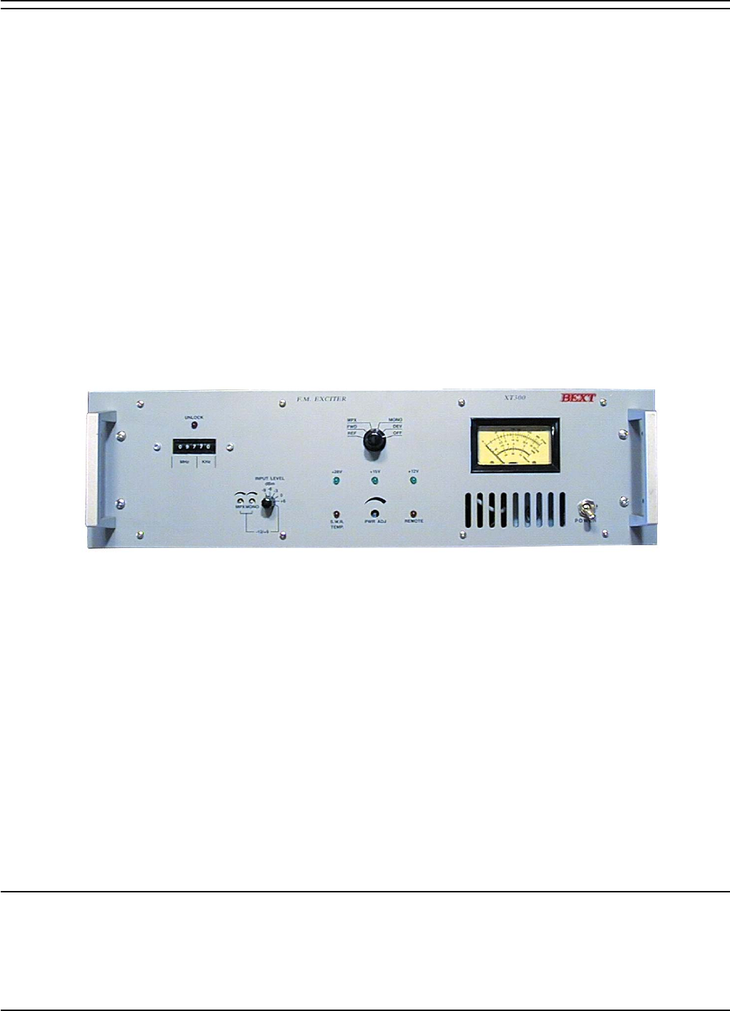
The XT150 is housed in a 3U, 19" rack-mouting container comprising a number of
interconnected modules mounted internally on the main chassis, facilitating
removal and substitution.The power output control, audio input level control
and analog meter for the measurement of operating parameters, are all mounted
on the front panel.
The line power, audio input, RF output and telemetry (optional) connectors are
mounted on the rear panel.
1.2 ELECTRICAL DESCRIPTION1.2 ELECTRICAL DESCRIPTION
1.2 ELECTRICAL DESCRIPTION1.2 ELECTRICAL DESCRIPTION
1.2 ELECTRICAL DESCRIPTION
The XT150 is an exciter working in the 87.5 to 108 MHz band, programmable in
steps of 10KHz. Its power output is continuously adjustable from 10W to 150W
into a 50 Ohm load.
The XT150 incorporates a stereo coder which guarantees excellent stereo
separation together with low harmonic distortion (only for Stereo version). It
also accepts two SCA signals. A front panel switch allows stereo operation (only
for stereo version) or "mono/mpx" operation which excludes the stereo encoder
and uses the "right" input as the mono input and the "left" input as the wideband
composite input. The specification features low audio distortion and
intermodulation figures (typically 0.03%) and a high signal-to-noise ratio
(typically -80 dB). A voltage selector on the transformer primary allows a variety
of supply voltages to be used.
1.3 METERS AND INDICATORS1.3 METERS AND INDICATORS
1.3 METERS AND INDICATORS1.3 METERS AND INDICATORS
1.3 METERS AND INDICATORS
The operating parameters of the exciter can be monitored using the analog
multimeter (12 Fig.1A and 8 Fig.1B) situated on the front panel. The parameter
to be measured is selected by the rotary selector (11 Fig.1A and 7 Fig.1B). The
frequency control (10 Fig.1A and 14 FIg.1B) allows frequencies to be selected
in steps of 10KHz. Three red alarm leds indicate VCO unlock (15 Fig.1A and 11
Fig.1B), excess VSWR on the output and the excess of temperature (4 Fig.1A and
8 Fig.1B), and the shutdown condition, programmed by a remote command (10 Fig.1A
and 6 Fig.1B). Three green leds (7 Fig.1A and 3 Fig.1B) indicate the presence
of +12V, +15V and +28V voltages which are used to power the various cards inside
the exciter. A selector (2 Fig.1A) allows selection between Mono/MPX and Stereo
functions and another selector (6 Fig.1A and 2 Fig.1B) is provided to choose
the level of the input signal. Trimmers are provided for adjustment of left and
right channels (5 Fig.1A and 1 Fig.1B) and a switch allows the stereo subcarrier
to benabled or disabled (3 Fig.1A).
1.4 AUTOMATIC FREQUENCY CONTROL1.4 AUTOMATIC FREQUENCY CONTROL
1.4 AUTOMATIC FREQUENCY CONTROL1.4 AUTOMATIC FREQUENCY CONTROL
1.4 AUTOMATIC FREQUENCY CONTROL
The operating frequency is governed by a thermally-compensated, reference

XT150 and XT150S Technical and Maintenance Manual
Pag. 5
oscillator working within a phase-locked loop (PLL). The XT150 reaches frequency
lock within a maximum of 30 seconds.
1.5 CONTROL CIRCUITS1.5 CONTROL CIRCUITS
1.5 CONTROL CIRCUITS1.5 CONTROL CIRCUITS
1.5 CONTROL CIRCUITS
The control circuits allow automatic control of output power(internal and
external), maintaining the chosen power level across the entire operating band.
Furthermore another circuit protects the final stage against excessive VSWR or
short circuits and excessive temperature. Then, there are other protection
circuits that allow to limit the maximum output power and to protect the equipment
against a power supply's overvoltage.
1.6 R.F. AMPLIFIER1.6 R.F. AMPLIFIER
1.6 R.F. AMPLIFIER1.6 R.F. AMPLIFIER
1.6 R.F. AMPLIFIER
The RF amplifier is a wide-band design and guarantees an adjustable power output
of 10 to 150 watts across the entire band. A low-pass filter enables the TEX150
to be used as a low power transmitter, connected directly to an antenna.
1.7 TECHNICAL SPECIFICATIONS1.7 TECHNICAL SPECIFICATIONS
1.7 TECHNICAL SPECIFICATIONS1.7 TECHNICAL SPECIFICATIONS
1.7 TECHNICAL SPECIFICATIONS
Please refer to Table (A) for the electrical specifications and Table (B) for
the mechanical specifications.

XT150 and XT150S Technical and Maintenance Manual
Pag. 6
TABLE A
ELECTRICAL SPECIFICATIONSELECTRICAL SPECIFICATIONS
ELECTRICAL SPECIFICATIONSELECTRICAL SPECIFICATIONS
ELECTRICAL SPECIFICATIONS
Power Supply 100-130V, 50-60Hz
198-250V, 50-60Hz
Power Consumption approx. 350W
Cooling Forced ventilation
Frequency Range from 87.5 to 108MHz in steps
of 10KHz
Output Power adjustable from 10 to 100 W
Automatic Output Level Control Stabilizes the set RF output
level
Output Impedance 50 Ohm
Output Connector Standard "N-type"
Harmonic Suppression > -65dB
Spurious Signal Suppression > -80dB
Mono Intermodulation Distortion 0.05 % or less, measured at
1KHz and 1.3 KHz, ratio 1:1 at
100% modulation
Frequency Stability ±500Hz (typ. ±300Hz) from 0°
to 50°C
Modulation Type Direct frequency modulation of
the RF oscillator at
fundamental frequency
Frequency Deviation ±75KHz nominal
Harmonic Distortion < 0.05% (typically 0.01%)
FM Signal-to-Noise Ratio > 75 dB mono, > 70 dB stereo
measured with 75KHz deviation
in the 30Hz to 15KHz band RMS.
Residual AM (Asynchronous) approx. 0.05%=65dB RMS
Residual AM (Synchronous) 0.1%=60dB
Pre-emphasis 50µs ±2% or 75µs ±2%
selectable

XT150 and XT150S Technical and Maintenance Manual
Pag. 7
Audio Input Impedance 10KOhm balanced or 5Kohm
unbalanced (600ohm on request)
Audio Input Level Selectable from -9 to +6 dBm
in five steps continuosly
from -12 to +9 dBm
Audio Frequency Range 30-15000Hz, MONO input
30-100000Hz, MPX input
Audio Input Filter > 45dB at 19KHz (Mono)
> 40dB from 20KHz to 100KHz
Mono Frequency Response ±0.3dB from 30Hz to 15KHz
MPX Frequency Response ±0.5dB from 30Hz to 75KHz
Stereo Separation > 45dB (typ. 50dB)
Pilot Tone Frequency 19KHz ± 1Hz
Pilot tone level -20dBm adjustable
Number of SCA inputs 2
SCA input impedance 1KOhm unbalanced
SCA input level 0dBm per ± 7.5KHz of deviation
SCA input response ± 0.5dBm from 40KHz to 100KHz

XT150 and XT150S Technical and Maintenance Manual
Pag. 8
TABLE B
MECHANICAL SPECIFICATIONSMECHANICAL SPECIFICATIONS
MECHANICAL SPECIFICATIONSMECHANICAL SPECIFICATIONS
MECHANICAL SPECIFICATIONS
Rack dimensions 483.00 mm (19.0") W
132.50 mm (5.20") H
345.00 mm (13.7") D
Operating temperature from -10°C to 50°C
Humidity 95% max., non-condensing
Weight 12 Kg

XT150 and XT150S Technical and Maintenance Manual
Pag. 9
CHAPTER 2
ELECTRICAL DESCRIPTIONELECTRICAL DESCRIPTION
ELECTRICAL DESCRIPTIONELECTRICAL DESCRIPTION
ELECTRICAL DESCRIPTION
2.1 INTRODUCTION2.1 INTRODUCTION
2.1 INTRODUCTION2.1 INTRODUCTION
2.1 INTRODUCTION
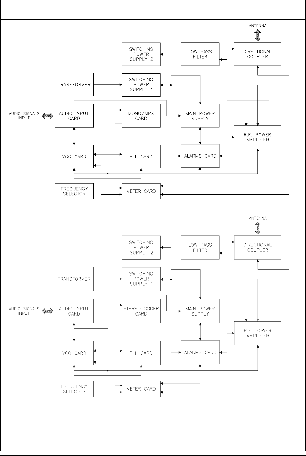
This section describes, in detail, the operating theory behind the
XT150. To aid understanding, the unit has been subdivided into
blocks, each of which is fully described below. The block diagram
is shown in Fig.3.
2.2 POWER SUPPLY2.2 POWER SUPPLY
2.2 POWER SUPPLY2.2 POWER SUPPLY
2.2 POWER SUPPLY
This circuit comprises a board, mounted on a heat sink, which is fixed
to the central part of the lower section of the unit (2 Fig.5). The power
supply generates the various stabilized voltages necessary for each of
the various modules that make up the XT150. The transformer has a
selectable input from 110 V to 240 V and two outputs A +18V (6.3A) and
B +32V (10A). This power supply is composed of two main parts: after
having undergone filtering for mains-borne interference, the supply is
transformed into four lower voltages, rectified, smoothed and
stabilized to the following values: +12V, +15V and 10 to 28V variable
to obtain the high efficiency (85-90%). The +15V supplies the encoder
mixer, the PLL card, the VCO card, the meter 100 card and the alarm card.
The +12V supplies the input of RF power amplifier driver (BGY33) and
the 10-28V variable supplies the output of RF power amplifier driver
(BGY33) and the final power stage of the same module (two MRF317 or two
SD1480).
The variable voltage of the final stage is controlled by the PWR ADJ
control which determines the R.F. power output of the exciter. The
automatic control of output power guarantees the power level set by the
PWR ADJ control right across the frequency range and independantly of
other variables such as temperature, load variations etc. The system
works by comparing the value set by the PWR ADJ control with the actual
power output of the unit and compensating accordingly. The final stage
driveris composed of two separate parts, the input part is supplied with
+12V voltage, and the output part is supplied by the switching power
supply with 4-12V variable voltage obtained dividing the 10-28V
variable voltage. A power limiting circuit intervenes in the event
of excess SWR on the output, thus protecting the final stage.
2.3 AUDIO INPUT CARD2.3 AUDIO INPUT CARD
2.3 AUDIO INPUT CARD2.3 AUDIO INPUT CARD
2.3 AUDIO INPUT CARD
This card is situated on the rear panel of the exciter (1 Fig.4 and 3
Fig.5). The card filters all audio signal inputs to the unit, removing
RF interference, before supplying them to the encoder mixer or Mono\MPX
card. The main operating parameters of the exciter are available for
remote monitoring via a telemetry connector.

XT150 and XT150S Technical and Maintenance Manual
Pag. 10
2.4 CODER MIXER (only for Stereo Version)2.4 CODER MIXER (only for Stereo Version)
2.4 CODER MIXER (only for Stereo Version)2.4 CODER MIXER (only for Stereo Version)
2.4 CODER MIXER (only for Stereo Version)
This card is situated in the lower part of the unit (6 Fig.4).
The card can function either as a stereo encoder or as a simple mixer
for the various audio inputs. The function may be selected by a
control situated on the front panel. In stereo encoder mode, the 19KHz
pilot tone is derived from a quartz crystal reference oscillator. So
too is the sampling
frequency which allows the L and R signals to be separated from the
multiplexed signal, plus the suppression of the 38KHz frequency. The
level of the left and right signals is set by the corresponding selector
situated on the front panel. The signals are then filtered at 15KHz and
pre-emphasized (50µS CCIR, 75µS FCC) before being sent to the multiplex
circuit. The audio signals from the two SCA inputs are mixed in to provide
the output. In mixer mode (Mono MPX) the stereo encoder is bypassed,
the right input accepts a mono signal and the left input accepts a
multiplex signal upto 100KHz. The SCA inputs remain unchanged. Three
rectifiers allow the peak levels of the two inputs "Left/MPX" and "right/
mono" to be displayed on the analog meter, and provide the audio detector
circuit with the deviation level.
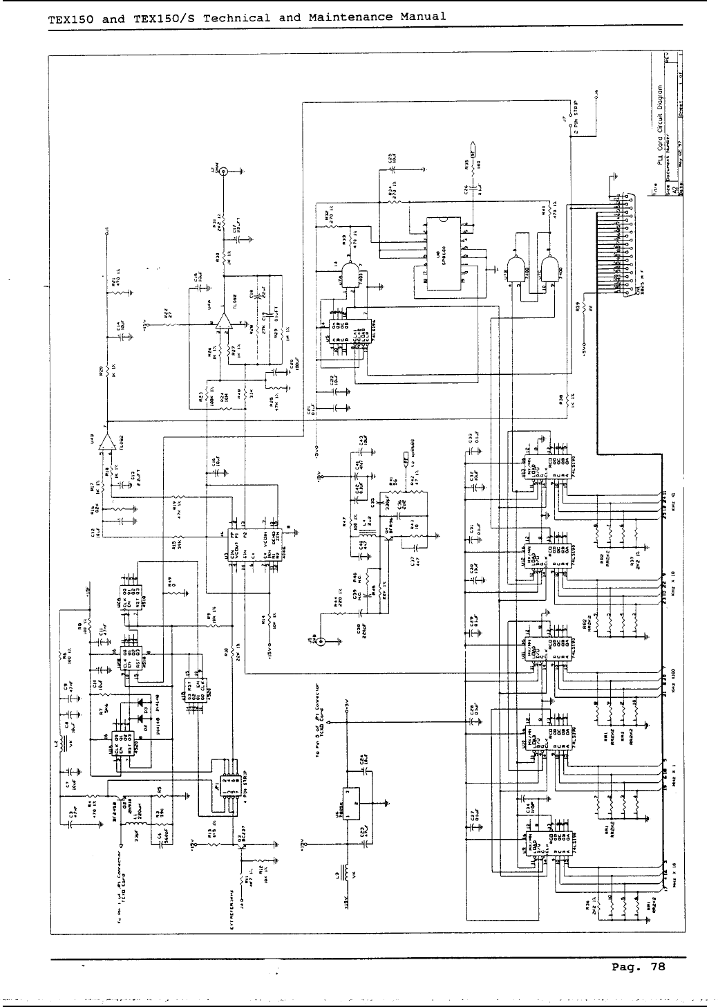
2.5 PLL CARD2.5 PLL CARD
2.5 PLL CARD2.5 PLL CARD
2.5 PLL CARD
The PLL card is situated internally, in the upper part of the unit (6
Fig.5). The circuit includes a reference cristal oscillator (optional
high stability), a logic section that includes the frequncy dividers
and comparator. The reference cristal oscillator generates a 4MHz
frequency that is divided to generate a 1KHz fixed signal. This signal
is compared to the operating frequency generated by the VCO divided
opportunely on the ground of the frequency setted on the Contraves. An
indicator situated on the front panel signals the "unlocked" condition.
The comparator output (AFC signal) is sent to the varicap diodes situated
on the VCO Card.
2.6 VCO CARD2.6 VCO CARD
2.6 VCO CARD2.6 VCO CARD
2.6 VCO CARD
The VCO card is situated internally, in the upper part of the unit
(4 Fig.4). This module includes an audio input stage at low frequency,
a voltage controlled oscillator at low noise (VCO) and a driver stage.
The audio signal supplied by the encoder mixer is amplified and then
injected into the VCO to provide class F3 modulation. The voltage
controlled oscillator (VCO) generates the signal on the frequency setted
on the Contraves. This signal is amplified to 300 mW level (25dBm) to
drive the final stage and to be sent to PLL circuit situated on the PLL
card. The operating frequency genereted by the VCO is divided down before

XT150 and XT150S Technical and Maintenance Manual
Pag. 11
being compared to a reference frequency, generated by a high stability
oscillator (standard 5ppm). The error voltage is filtered and used to
compensate the VCO frequency and guarantee its stability. A trimmer is
present on this card for adjustment of deviation.
2.7 R.F. POWER AMPLIFIER2.7 R.F. POWER AMPLIFIER
2.7 R.F. POWER AMPLIFIER2.7 R.F. POWER AMPLIFIER
2.7 R.F. POWER AMPLIFIER
The final power stage is mounted on a heat sink to dissapate waste heat
and is enclosed in a totally screened, metal container, fixed to the
upper-middle part of the central section of the unit (1 Fig.5). The RF
signal coming from the Stereo Decoder or Mono\MPX at a power level of
about 300 mW, reaches the driver stage (BGY33) and is amplified to a
level from about 1W to 20 W before being further amplified by the final
stage (two MRF317 or two SD1480) to a level of upto 150 W. The resultant
signal is then filtered by a low-pass filter (2 Fig.5) which removes
any harmonic content.A directional coupler allows the direct and
reflected power levels to be measured and displayed on the analog
multimeter and also fedback to the power supply for automatic control
of the output power (see Power Supply description). A BNC connector
situated on the rear panel provides a power signal at -40 dB of the
amplifier output power.
2.8 METER CARD2.8 METER CARD
2.8 METER CARD2.8 METER CARD
2.8 METER CARD
This card is situated centrally on the front panel (5 Fig.4 and 7 Fig.5).
The card receives direct and reflected power signals from the power
supply which, in turn, come from the final power stage. The Stereo
encoder card supplies deviation and left and right signal levels.
These signal levelsare then displayed on the analog meter according to
the position of therotary selector situated on the front panel.
2.9 CONTRAVES CARD2.9 CONTRAVES CARD
2.9 CONTRAVES CARD2.9 CONTRAVES CARD
2.9 CONTRAVES CARD
This card is fixed to the left-hand side of the front panel (5 Fig.5).
The operating frequency selected by the frequency control is represented
by a signal which is supplied to the frequency dividers that form part
of the PLL circuits found on the PLL card.
2.10 ALARMS CARD2.10 ALARMS CARD
2.10 ALARMS CARD2.10 ALARMS CARD
2.10 ALARMS CARD
This card is fixed in the lower part of the unit (7 Fig.4). This circuit
allows to adjust, through 7 trimmers, the threeshold of the external
and internal output level, internal and external VSWR level, temperature
and to preset the maximum value of the output power. In case of fault
there isn't an automatic reset, because the transmitter provides to
decrease the output power to continue the transmission without
stops,even if at minimum power.

XT150 and XT150S Technical and Maintenance Manual
Pag. 12
2.11 MONO\MPX CODER CARD (Mono Version)2.11 MONO\MPX CODER CARD (Mono Version)
2.11 MONO\MPX CODER CARD (Mono Version)2.11 MONO\MPX CODER CARD (Mono Version)
2.11 MONO\MPX CODER CARD (Mono Version)
This card is fixed in the lower part of the unit. The Mono\MPX card is
an Audio Mixer at four inputs, two balanced (Mono and MPX) and two
unbalanced (SCA1 and SCA2). Mono and MPX input level can be setted
through relative switches placed on front panel, on 5 fixed positions
and on a variable position from -12dBm to +9dBm (pre-setted at 0dBm).
It's possible to set the pre-enphasis value at 50µS, 75µS or linear.
Then, it's possible to insert or remove a low pass filter at 15KHz.
2.12 CLIPPER CARD (Optional)2.12 CLIPPER CARD (Optional)
2.12 CLIPPER CARD (Optional)2.12 CLIPPER CARD (Optional)
2.12 CLIPPER CARD (Optional)
This card is fixed with a sandwich structure on the coder card and is
accesible from lower part of the equipment. Its function is that
to limit drastically any audio signal that exceeds a prefixed
threshold. Therefore, it's used to avoid any type of over-modulation
as to maximum peak permitted of ± 75KHz. With an exceeding signal,
immediately too, of 6 dB the nominal
level for a deviation of ± 75KHz, this card allows to contain deviation
increasing within 1dB.
FRONT PANEL STEREO VERSION VIEW DESCRIPTION (FIG.1A)FRONT PANEL STEREO VERSION VIEW DESCRIPTION (FIG.1A)
FRONT PANEL STEREO VERSION VIEW DESCRIPTION (FIG.1A)FRONT PANEL STEREO VERSION VIEW DESCRIPTION (FIG.1A)
FRONT PANEL STEREO VERSION VIEW DESCRIPTION (FIG.1A)
1 STEREO/MONO-MPX Selects STEREO or MONO/MPX operation
2 STEREO LED Indicates the operation of the stereo encoder
3 19KHz LED Indicates the 19KHz pilot tone presence
4 MODE SELECTOR Button in: STEREO OPERATION MODE pilot tone
present
Button out: MONO OPERATION MODE pilot tone
absent
5 L/MPX & R/MONO LEVEL L/MPX and R/Mono input level adjustable from
-12 to +9 dBm; this is possible if the input
level switch is completely turned clockwise
6 INPUT LEVEL Input signal attenuator adjustable in
5 steps from -9 to +6 dBm
7 VOLTAGES LEDS Indicates the presence of the internal
operating voltages +12V, +15V and +28V
8 SWR Indicates that reflected power exceeds 10W
9 PWR ADJ 10-turn trimmer to regulate the power output
of the exciter. AGC maintains the level set by
this control
10 REMOMTE Indicates that the exciter has been shut-down
by remote control

XT150 and XT150S Technical and Maintenance Manual
Pag. 13
11 MEASUREMENT SELECTOR The measurement made by the meter corresponds
to the position of this selector
12 METER Analog meter used to display the following
operating parameters of the exciter:
Direct power f.s. 200W
Reflected power f.s. 50W
Deviation f.s. 100KHz
Right channel input level f.s. +3dB
Left channel input level f.s. +3dB
13 POWER ON/OFF switch
14 MHz/KHz Rotary frequency selector
15 L.O. UNLOCK If ON indicates that the VCO is not locked to
the reference frequency. The output power will
drop to zero in this condition
FRONT PANEL MONO VERSION VIEW DESCRIPTION (FIG.1B)FRONT PANEL MONO VERSION VIEW DESCRIPTION (FIG.1B)
FRONT PANEL MONO VERSION VIEW DESCRIPTION (FIG.1B)FRONT PANEL MONO VERSION VIEW DESCRIPTION (FIG.1B)
FRONT PANEL MONO VERSION VIEW DESCRIPTION (FIG.1B)
1 L/MPX & R/MONO LEVEL L/MPX and R/Mono input level adjustable from
-12 to +9 dBm
2 INPUT LEVEL Input signal attenuator adjustable in 5 steps
from -9 to +6 dBm
3 VOLTAGES LEDS Indicates the presence of the internal
operating voltages +12V, +15V and +28V
4 SWR Indicates that reflected power exceeds 10W
5 PWR ADJ 10-turn trimmer to regulate the power output
of the exciter. AGC maintains the level set by
this control
6 REMOTE Indicates that the exciter has been shut-down
by remote control
7 MEASUREMENT SELECTOR The measurement made by the meter corresponds
to the position of this selector
8 METER Analog meter used to display the following
operating parameters of the exciter:
Direct power f.s. 200W
Reflected power f.s. 50W
Deviation f.s. 100KHz
Right channel input level f.s. 3dB
Left channel input level f.s. 3dB
9 POWER Supply on/off switch
10 MHz/KHz Rotary frequency selector
11 L.O. UNLOCK Indicates that the VCO is not locked to the
reference frequency. The output power will
drop to zero in this condition
XT150 and XT150S Technical and Maintenance Manual
Pag. 14
FIG. 1A
XT150 and XT150S Technical and Maintenance Manual
Pag. 15
FIG. 1BFIG. 1B
FIG. 1BFIG. 1B
FIG. 1B

XT150 and XT150S Technical and Maintenance Manual
Pag. 16
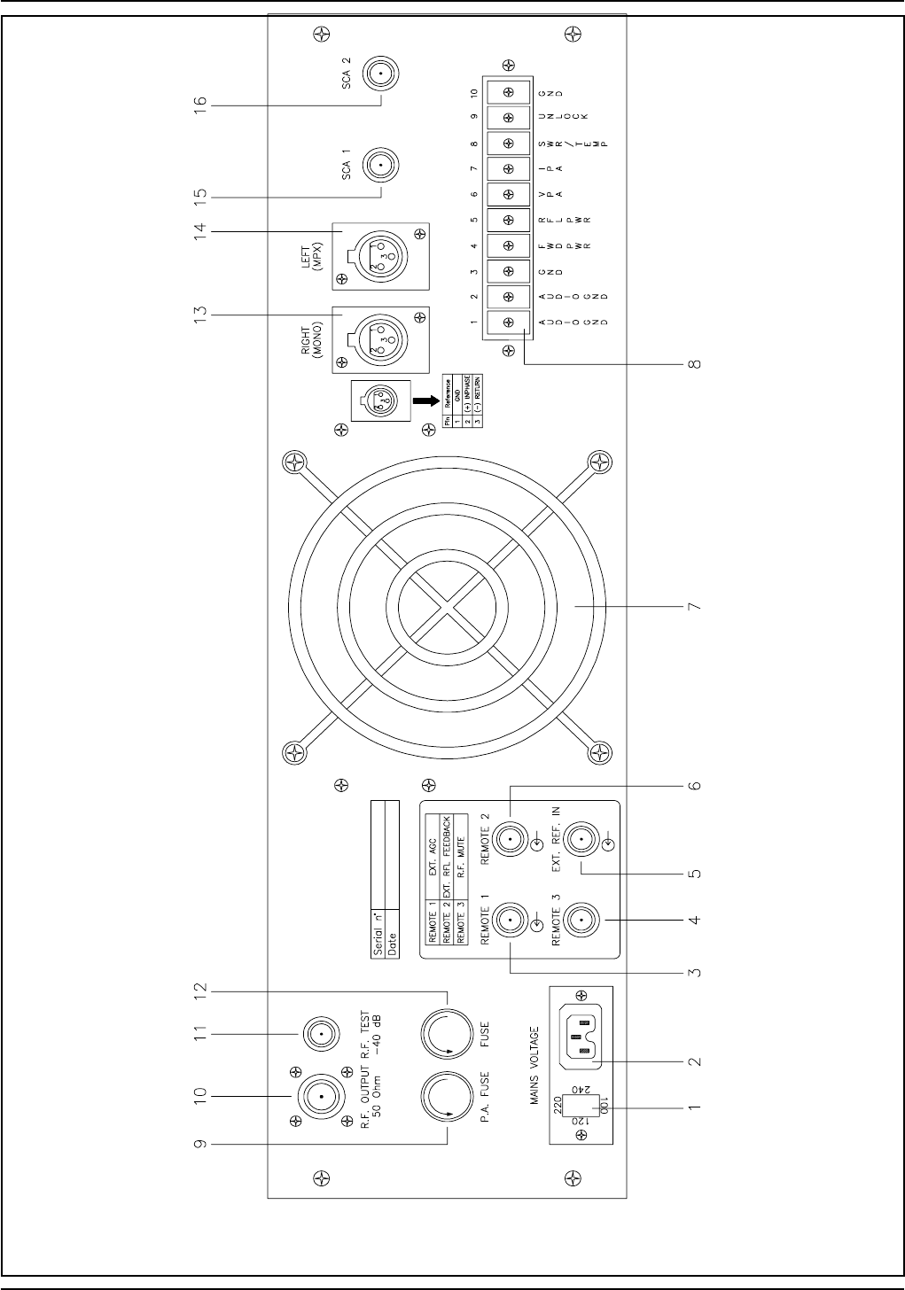
REAR PANEL VIEW DESCRIPTIONREAR PANEL VIEW DESCRIPTION
REAR PANEL VIEW DESCRIPTIONREAR PANEL VIEW DESCRIPTION
REAR PANEL VIEW DESCRIPTION
(FIG. 2)(FIG. 2)
(FIG. 2)(FIG. 2)
(FIG. 2)
1 FUSE BLOCK Fuse block and line voltage selector. Use a
small screwdriver to change the fuse or the
line voltage. Rotate the block and position it
for the desired voltage.
2 PLUG Line power connector
3 REMOTE 1 BNC connector, External AGC input
4 REMOTE 2 BNC connector, External Reflected Feedback
input
5 EXT REF 1 KHz External 1 KHz reference (optional)
6 REMOTE 3 BNC connector. Connecting the central
conductor to ground will cause the RF output
power level to drop to zero and to stay there
until the short is removed. When used with an
R.V.R. amplifier, this connector should be
connected to the "REMOTE" output of the power
amplifier.
7 FAN Fan-assisted cooling for the power stage and
the power supply.
8 TELEMETRY TERMINALS 10-pin telemetry card
1-2-3-10 GND
4 Forward power
5 Reflected power
6 VPA
7 IPA
8 SWR alarm
9 Unlock alarm
9 P.A. FUSE Power Amplifier Protection fuse 8A
10 R.F. OUTPUT N-type connector, 50 Ohm
11 R.F. TEST POINT -40 dB output referred to the output power
level
12 FUSE Main Protection Fuse 6A
13 RIGHT (MONO) BNC connector for FCC unbalanced version;
Cannon XLR for CCIR version with balanced
input
14 LEFT (MPX) BNC connector for FCC version; Cannon XLR for
CCIR version with balanced input
15 SCA 1 BNC connector, unbalanced SCA1 input
16 SCA 2 BNC connector, unbalanced SCA2 input or output
(internally selactable) for pilot tone (i.e.
for RDS encoder)
XT150 and XT150S Technical and Maintenance Manual
Pag. 17
FIG. 2FIG. 2
FIG. 2FIG. 2
FIG. 2
XT150 and XT150S Technical and Maintenance Manual
Pag. 18
MONO VERSION BLOCK DIAGRAM (FIG.3A)MONO VERSION BLOCK DIAGRAM (FIG.3A)
MONO VERSION BLOCK DIAGRAM (FIG.3A)MONO VERSION BLOCK DIAGRAM (FIG.3A)
MONO VERSION BLOCK DIAGRAM (FIG.3A)
STEREO VERSION BLOCK DIAGRAM (FIG.3B)STEREO VERSION BLOCK DIAGRAM (FIG.3B)
STEREO VERSION BLOCK DIAGRAM (FIG.3B)STEREO VERSION BLOCK DIAGRAM (FIG.3B)
STEREO VERSION BLOCK DIAGRAM (FIG.3B)

XT150 and XT150S Technical and Maintenance Manual
Pag. 19
TOP VIEW DESCRIPTION (FIG.4)TOP VIEW DESCRIPTION (FIG.4)
TOP VIEW DESCRIPTION (FIG.4)TOP VIEW DESCRIPTION (FIG.4)
TOP VIEW DESCRIPTION (FIG.4)
1 .................... Audio Input Card
2 .................... Power Supply Card
3 .................... Switch Power Supply 1
4 .................... Anolog Meter
5 .................... Meter Card
6 .................... Stereo Coder Card (for Stereo Version)
Mono\MPX Card (for Mono Version)
7 .................... Alarms Card
8 .................... Analog Meter
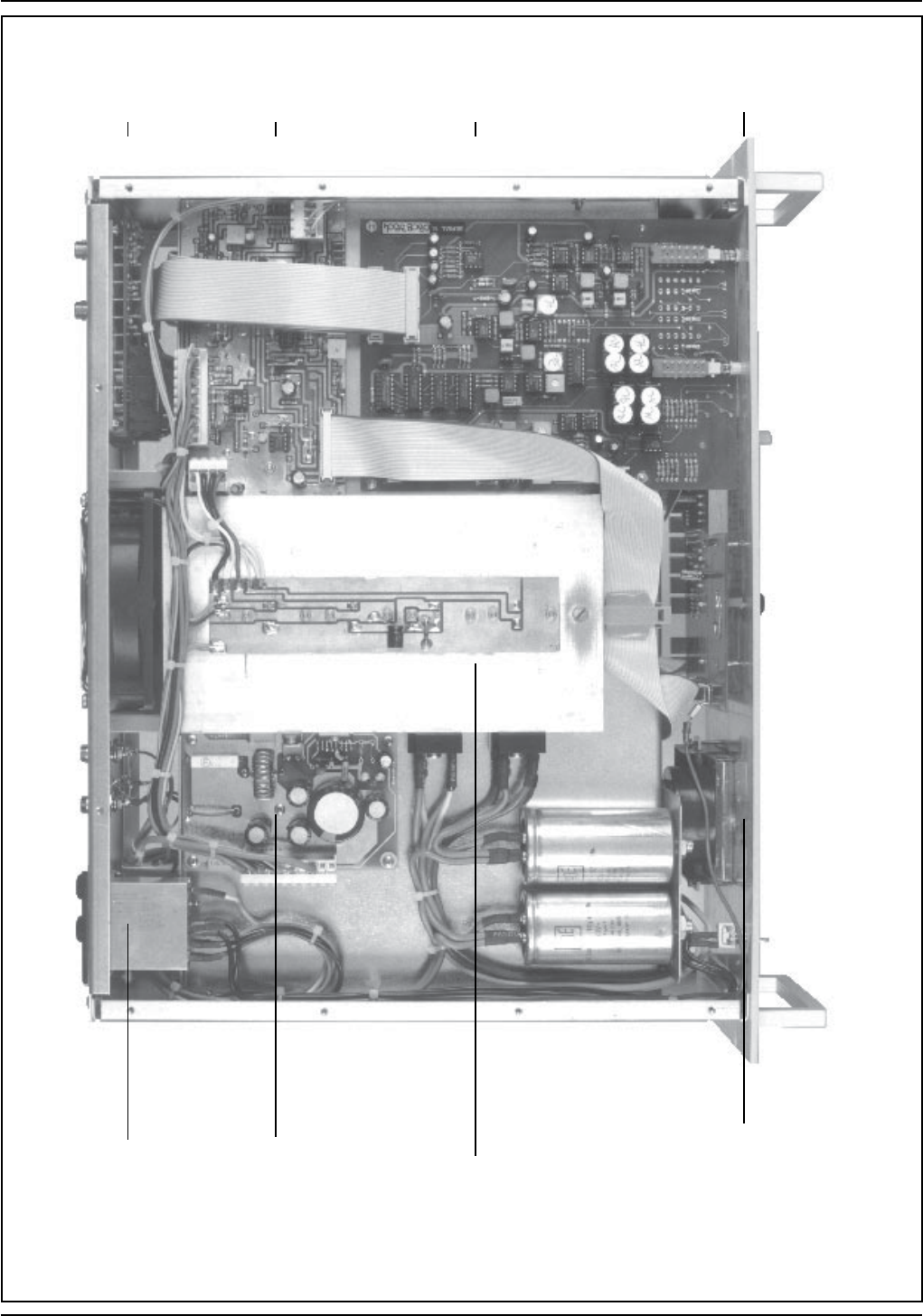
XT150 and XT150S Technical and Maintenance Manual
Pag. 20
FIG.4FIG.4
FIG.4FIG.4
FIG.4
1 7 6 5
8 3 2 4

XT150 and XT150S Technical and Maintenance Manual
Pag. 21
DOWN VIEW DESCRIPTION (FIG.5)DOWN VIEW DESCRIPTION (FIG.5)
DOWN VIEW DESCRIPTION (FIG.5)DOWN VIEW DESCRIPTION (FIG.5)
DOWN VIEW DESCRIPTION (FIG.5)
1 .................... Power Amplifier Card
2 .................... Low Pass Filter
3 .................... Audio Input Card
4 .................... VCO Card
5 .................... Frequency Selector Card
6 .................... PLL Card
7 .................... Meter Card
8 .................... Switching Power Supply 2
9 .................... Toroidal transformer
10 .................... Directional Coupler
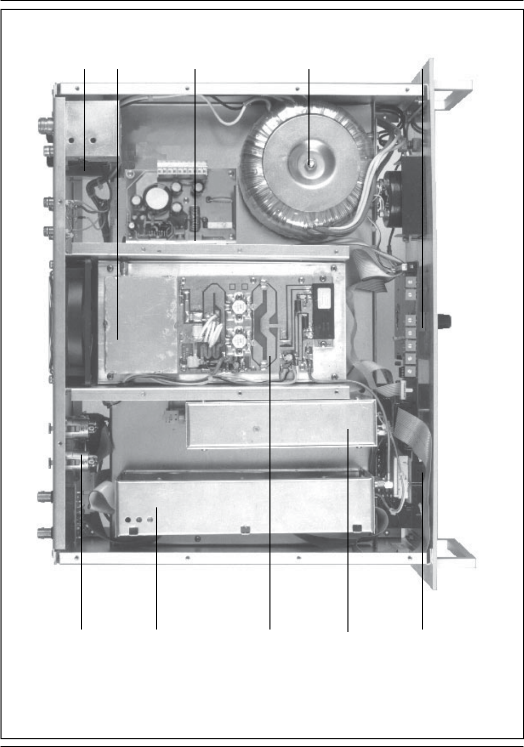
XT150 and XT150S Technical and Maintenance Manual
Pag. 22
FIG. 5FIG. 5
FIG. 5FIG. 5
FIG. 5
102897
36 145

XT150 and XT150S Technical and Maintenance Manual
Pag. 23
TABLE C
RECOMMENDED TEST EQUIPMENTRECOMMENDED TEST EQUIPMENT
RECOMMENDED TEST EQUIPMENTRECOMMENDED TEST EQUIPMENT
RECOMMENDED TEST EQUIPMENT
INSTRUMENTINSTRUMENT
INSTRUMENTINSTRUMENT
INSTRUMENT MODELMODEL
MODELMODEL
MODEL SPECIFICATIONSPECIFICATION
SPECIFICATIONSPECIFICATION
SPECIFICATION
Coaxial Load Resistor Bird Power Rating 300W continuous
Mod. 8173
Wattmeter Bird Power Range: 100mW to 10KW
Mod. 43 using Bird Plug-in-Elements
Frequency Range: 0.45 to
2300MHz
Plug-in-Elements Bird Power Rating: 250W
Freq. Range: 50 to 125MHz
Stereo Decoder A.E.V. Stereo Separation: > 60 dB
Mod. SMD from 30Hz to 15 KHz
Low Distorsion Krohn-Hite THD < 0.001%
A.F. Generator Mod. 4400A
Oscilloscope Tektronix 100MHz Oscilloscope
Mod. 2247A Counter/Timer
F.M. Modulation Meter Rohde Schwarz
Mod. F.A.M.
Digital Multimeter Metrix
XT150 and XT150S Technical and Maintenance Manual
Pag. 24
CHAPTER 3
INSTALLATION PROCEDURESINSTALLATION PROCEDURES
INSTALLATION PROCEDURESINSTALLATION PROCEDURES
INSTALLATION PROCEDURES
3.1 INTRODUCTION3.1 INTRODUCTION
3.1 INTRODUCTION3.1 INTRODUCTION
3.1 INTRODUCTION
This chapter contains the information required for installation of the
TEX150 exciter and for preliminary checks.
3.2 UNPACKING3.2 UNPACKING
3.2 UNPACKING3.2 UNPACKING
3.2 UNPACKING
Remove the unit from its packaging and before any other operation, check
for any damage that the unit may have suffered in transit and that all
front and rear panel controls are functioning.
3.3 INSTALLATION3.3 INSTALLATION
3.3 INSTALLATION3.3 INSTALLATION
3.3 INSTALLATION
1)Check that the line voltage selector is correctly set for the local
supply. If not, remove the cover on which the voltages are printed
and rotate it until the required value corresponds to the arrow,
and reinsert it. Check also that the fuse (1 Fig.2) mounted inside the
cover is present and in order.
The current capacity of the fuse are as follows:
220-240 V - 6.3 A
100-120 V - 12 A
2)Now ensure that the PWR ADJ control (9 Fig.1A or 5 Fig.1B) is rotated
fully anti-clockwise, using a small screwdriver. N.B. The control is
a ten-turn potentiometer so care should be taken to verify the minimum
position.
Units are usually shipped with this control already at minimum.
WARNING: When the unit is switched on with the control at its minimum
position, power output is about 10W.
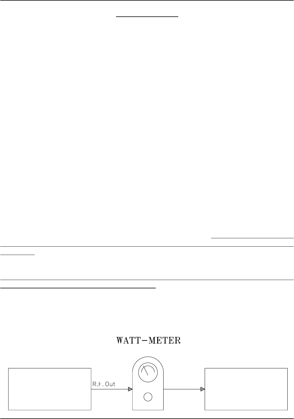
3)Connect a dummy load with a power rating of at least 150 W continuous
to the RF output, situated on the rear panel of the unit. It is advisable
to connect a bypass wattmeter in series with this load in order to verify
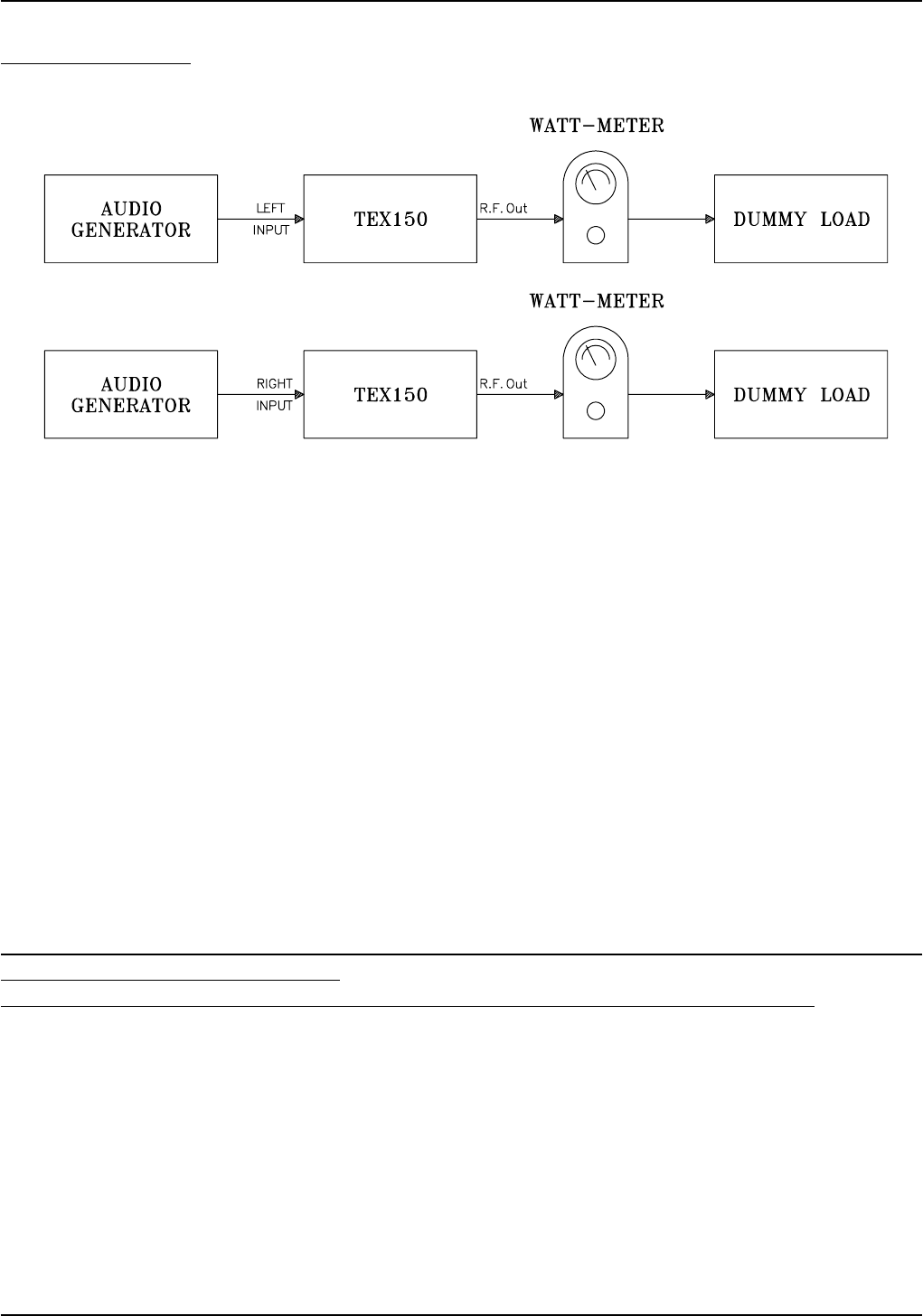
the accuracy of the unit's own internal wattmeter (see SETUP 1).
SETUP 1SETUP 1
SETUP 1SETUP 1
SETUP 1
XT150 DUMMY LOAD

XT150 and XT150S Technical and Maintenance Manual
Pag. 25
4)Connect a switch, via a cable, to the REMOTE 3 connector (4 Fig.2)
on the rear panel so that the switch is able to short the central
conductor to its screen. Leave the switch in the short-circuit position.
5)Switch the unit's ON/OFF switch (13 Fig.1A or 9 Fig.1B) to the OFF
position.
6) Connect line power to the unit via the VDE socket (2 Fig.2).
Note: It's essential that the unit be properly earthed to ensure both
the safety of the operator as well as the correct functioning of the
equipment.
7)Switch the power On switch (13 Fig.1A or 9 Fig.1B) to the ON position
and check that the three green internal voltage led (7 Fig.1A or 3 Fig.1B)
and the red UNLOCK led (15 Fig.1A or 11 Fig.1B) are all on. Select the
desired operating frequency using the corresponding selector. The red
UNLOCK led should switch off within 30 seconds, indicating that the
oscillator has locked onto the operating frequency. The frequency se-
lector comprises five figures of which the three to the left of the
decimal point represent (from left to right) hundreds of MHz, tens of
MHz and MHz. The two figures to the right of the decimal point rep-
resent (from left to right) hundreds of KHz and tens of KHz.
Eg: 098.45 = ninety eight megahertz and four hundred and fifty
Kilohertz.
Eg: 103.94 = one hundred and three Megahertz and nine hundred and forty
Kilohertz.
Furthermore, if a frequency is selected beyond the two limits of the
87.5-108 MHz band, the amplifier will continue to work even through the
displayed frequency no longer corresponds to the operating frequency
of the unit.
Note: Transmitting outside the legal band (87.5-108 MHz) is an offenceNote: Transmitting outside the legal band (87.5-108 MHz) is an offence
Note: Transmitting outside the legal band (87.5-108 MHz) is an offenceNote: Transmitting outside the legal band (87.5-108 MHz) is an offence
Note: Transmitting outside the legal band (87.5-108 MHz) is an offence
and may lead to prosecution.and may lead to prosecution.
and may lead to prosecution.and may lead to prosecution.
and may lead to prosecution.
8)After having verified that the UNLOCK led is switched off and that
the unit is therefore locked to the selected operating frequency, switch
the switch connected to the REMOTE connector so as to remove the short
circuit between the central conductor and ground. The RF output is now
enabled and should correspond to a power level of about 10W. To check
this reading, select FWD on the meter selector and read the power from
the 200 W FSD scale.
9)Using a small screwdriver, rotate the PWR ADJ control clockwise; the
power output should increase progressively to a maximum of 100W.
Check the value with the bypass wattmeter which should be within ±10%.

XT150 and XT150S Technical and Maintenance Manual
Pag. 26
10)With the power output at 150W, select a new operating frequency well
away from the current value. Eg: 107 MHz: the UNLOCK led should switch
on and the power output should fall to zero at the same time. Only when
the UNLOCK led switches off (unit locked to new frequency) should the
power output resume its previous level.
11) Automatic power control check
It is advisable to start this procedure with the operating frequency
set to 87.50 MHz. When locked to this frequency, the PWR ADJ control
should be adjusted for an output power of 50 W. Now, with no further
adjustment of the PWR ADJ control, change the operating frequency in
steps of 4-5 MHz, ensuring that the output power remains constant at
50 W.
12) SWR alarm check
For this test, adjust the PWR ADJ control for a power output of 10W.
Disconnect the output load and check that the S.W.R. led switches on.
Now adjust the PWR ADJ control to check that the unit switches on again
at a reflected power level of about 20 W. Turn the PWR ADJ control for
maximum power and check that the reflected power does not exceed 50 W.
Re-connect the output load and check that REF falls to zero, the SWR
led switches off and that PWR FWD jumps to 150 W.
13) Now short circuit the central conductor of the REMOTE input to ground
and the output power should drop instantly to zero. Removing the short
should cause the power output to return, gradually, to its previous
level.
14) Deviation reading check
The maximum input sensitivity is determined by the position of the INPUT
LEVEL control. In the -12/+9 position, the sensitivity will d e -
pend on the L/mpx and R/mono controls. Put the selector in the DEV
position. Connect a low-distortion audio generator to the LEFT and RIGHT
inputs. Inject a 400 Hz tone at a level of 0dBm (775mVRMS= 2.2Vpp).Put the
INPUT LEVEL control in the 0dBm position. Select stereo mode (the
corresponding led will switch on). Enable the PILOT using the relevant
switch (the green led will switch on). With the selector in the R/MONO
position, check that the reading is 0b, measured on the +3dB FSD scale.
Repeat the operation for the L/MPX. Check that the deviation reading
is 100%.
3.33.3
3.33.3
3.3
1) Inject the pilot tone checking that the corresponding led switches
on.
3.43.4
3.43.4
3.4 OPERATION USING THE INTERNAL STEREO ENCODER (Only for Stereo Ver.)OPERATION USING THE INTERNAL STEREO ENCODER (Only for Stereo Ver.)
OPERATION USING THE INTERNAL STEREO ENCODER (Only for Stereo Ver.)OPERATION USING THE INTERNAL STEREO ENCODER (Only for Stereo Ver.)
OPERATION USING THE INTERNAL STEREO ENCODER (Only for Stereo Ver.)
1) Inject the pilot tone checking that the corresponding led switches
on.
XT150 and XT150S Technical and Maintenance Manual
Pag. 27
2) Select STEREO operation confirmed by the corresponding led.
3) Select the sensitivity of the audio LEFT/RIGHT inputs to match
the signal level being supplied to the unit. (CONT..PG.27)
4) Connect the signal source to the LEFT/RIGHT inputs. These are
balanced inputs (see SETUP 2).
SETUP 2SETUP 2
SETUP 2SETUP 2
SETUP 2
5)Check on the internal analog meter that the L/R signal levels are those
expected, selecting the desired input with the corresponding control.
6)The effective modulation level may be measured on the analog
multimeter by selecting DEV with the corresponding selector.
3.5 CONNECTION OF AN EXTERNAL STEREOPHONIC SOURCE3.5 CONNECTION OF AN EXTERNAL STEREOPHONIC SOURCE
3.5 CONNECTION OF AN EXTERNAL STEREOPHONIC SOURCE3.5 CONNECTION OF AN EXTERNAL STEREOPHONIC SOURCE
3.5 CONNECTION OF AN EXTERNAL STEREOPHONIC SOURCE
1)Connect the stereo source's output to the MPX input of the unit
(see SETUP 3).
SETUP 3SETUP 3
SETUP 3SETUP 3
SETUP 3
2)Adjust the stereo encoder to obtain just the 19 KHz subcarrier output
and ensure the total absence of signals on the left and right inputs
of the encoder.
3)Adjust the output level of the encoder to obtain the correct level
as displayed on the analog meter of the TEX150.
4)Inject audio signals into the left and right inputs of the encoder
and adjust the sensitivity of the input to obtain a peak reading
of MAX=75KHz with both channels enabled.
XT150 and XT150S Technical and Maintenance Manual
Pag. 28
3.6 MONOPHONIC TRANSMISSION3.6 MONOPHONIC TRANSMISSION
3.6 MONOPHONIC TRANSMISSION3.6 MONOPHONIC TRANSMISSION
3.6 MONOPHONIC TRANSMISSION
1)Connect the signal source (audio mixer, receiver, compressor etc.)
to the MONO input. This input is unbalanced (see SETUP 4).
SETUP 4SETUP 4
SETUP 4SETUP 4
SETUP 4
2)Select the desired INPUT LEVEL.
3)Adjust the signal level of the equipment connected to the TEX150
(with the audio signal present) for a peak reading of DEVIATION MAX
75 KHz.
Note that international standards permit a maximum deviation (DEV
MAX) of 75 KHz for frequency modulated, radiophonic transmissions.
Exceeding this limit will only result in the degradation of signal
quality.
In the case of mono transmissions, the stereo input is available for
frequencies between 15 KHz and 100 KHz (i.e. subcarriers for SCA,
RDS etc.).

XT150 and XT150S Technical and Maintenance Manual
Pag. 29
CHAPTER 4
MAINTENANCE PROCEDURESMAINTENANCE PROCEDURES
MAINTENANCE PROCEDURESMAINTENANCE PROCEDURES
MAINTENANCE PROCEDURES
4.1 SAFETY REQUIREMENTS4.1 SAFETY REQUIREMENTS
4.1 SAFETY REQUIREMENTS4.1 SAFETY REQUIREMENTS
4.1 SAFETY REQUIREMENTS
WARNING WARNING WARNING WARNING WARNING WARNING WARNING WARNING
When the exciter is operational, removing the top cover will expose
lethal voltages on the line voltage selector and heavy currents on the
power supply filter terminals and power transistors. Use insulated tools
for any type of maintenance work and do not touch any internal components
when the exciter is switched on.
Ensure that the exciter is disconnected from the line supply before
carrying out any maintenance work.
MAINTENANCE LEVEL 1MAINTENANCE LEVEL 1
MAINTENANCE LEVEL 1MAINTENANCE LEVEL 1
MAINTENANCE LEVEL 1
4.2 ROUTINE MAINTENANCE4.2 ROUTINE MAINTENANCE
4.2 ROUTINE MAINTENANCE4.2 ROUTINE MAINTENANCE
4.2 ROUTINE MAINTENANCE
The only routine maintenance required by the TEX150 is the periodic
replacement of the cooling fan and the removal of accumulated dust. The
period between such action will depend on ambient operating conditions
such as temperature, air-borne dust levels and humidity. It is advisable
to check the unit every 6 months and to replace noisy or worn fans. Fans
should be replaced as a matter of course after no more than 18 months
of operation.
MAINTENANCE LEVEL 2MAINTENANCE LEVEL 2
MAINTENANCE LEVEL 2MAINTENANCE LEVEL 2
MAINTENANCE LEVEL 2
4.3 STEREO ENCODER CARD REPLACEMENT4.3 STEREO ENCODER CARD REPLACEMENT
4.3 STEREO ENCODER CARD REPLACEMENT4.3 STEREO ENCODER CARD REPLACEMENT
4.3 STEREO ENCODER CARD REPLACEMENT
1)Open the top and bottom covers of the unit.
2)Disconnect connectors J1, J3 and J4.
3)Unscrew the four nuts fixing the card on internal chassis.
4)Unscrew the screw inside the INPUT LEVEL knob and slide it off.
5)Raise the card from its supports, simultaneously sliding the
switches and the INPUT LEVEL switch pivot from the panel.

XT150 and XT150S Technical and Maintenance Manual
Pag. 30
4.4 RF POWER AMPLIFIER TRANSISTOR REPLACEMENT4.4 RF POWER AMPLIFIER TRANSISTOR REPLACEMENT
4.4 RF POWER AMPLIFIER TRANSISTOR REPLACEMENT4.4 RF POWER AMPLIFIER TRANSISTOR REPLACEMENT
4.4 RF POWER AMPLIFIER TRANSISTOR REPLACEMENT
For this module it's only possible to replacement the transistors:
1)Open the top cover of the unit.
2)Open the top cover of the RF power amplifier.
3)Unscrew the two fixing screws of the device (BGY33, MRF317 or
SD1480).
4)Remove the broken transistor.
NOTE: During replacement of broken devices it's necessary to pay
attention to device's pin position and insertion, to check that the
device's fixing screws aren't in short-circuit and to check that the
soldering is good and without impurities.
NOTE: Interpose between devices and heat-sink an electronic silicone
compound.
4.5 VCO REPLACEMENT4.5 VCO REPLACEMENT
4.5 VCO REPLACEMENT4.5 VCO REPLACEMENT
4.5 VCO REPLACEMENT
1)Open the top cover of the unit.
2)Disconnect connectors CN1, CN2, J1, J3 and J4.
3)Desolder the two wires connected on J2 and J5 of the VCO Card.
4)Unscrew the fixing screws of the VCO card metal box on the internal
chassis.
5)Remove the metal box.
NOTE: For any adjustment is sufficient remove the top and bottom covers
of the metal box.
4.6 AUDIO INPUT CARD REPLACEMENT4.6 AUDIO INPUT CARD REPLACEMENT
4.6 AUDIO INPUT CARD REPLACEMENT4.6 AUDIO INPUT CARD REPLACEMENT
4.6 AUDIO INPUT CARD REPLACEMENT
1)Open the bottom cover of the unit.
2)Disconnect connectors CN1, and CN2.
3)Unscrew the nuts of the two connectors BNC1 and BNC2 situated on
the rear panel.
4)Unscrew the two screws fixing the telemetry terminals block,
situated on the rear panel.

XT150 and XT150S Technical and Maintenance Manual
Pag. 31
5)Desolder the six wires (placed on EC1 and EC2) connecting the Audio
Input Card to the two audio connectors, RIGHT (mono) and LEFT (MPX).
6)Slide the card out.
4.7 MAIN POWER SUPPLY'S TRANSISTORS REPLACEMENT4.7 MAIN POWER SUPPLY'S TRANSISTORS REPLACEMENT
4.7 MAIN POWER SUPPLY'S TRANSISTORS REPLACEMENT4.7 MAIN POWER SUPPLY'S TRANSISTORS REPLACEMENT
4.7 MAIN POWER SUPPLY'S TRANSISTORS REPLACEMENT
1)Open the top and bottom covers of the unit.
2)Remove from flat cable clamp the flatwire fixed on heat-sink.
3)Unscrew the two fixing screws of the components U1 and D1 of the
switching power supply (pay attention to device insulator).
4)Unscrew the two fixing screws of the two rectifier bridges.
5)Unscrew the fixing screws of the heat-sink and raise the top part
of heat-sink paying attention to cabling.
6)Desolder the device's pins.
7)Carefully lift out the device.
NOTE: During replacement of broken devices it's necessary to pay
attention to device's pin position and insertion, to check that the
device's fixing screws aren't in short-circuit and to check that the
soldering is good and without impurities.
NOTE: Interpose between devices and heat-sink an electronic silicone
compound.
4.84.8
4.84.8
4.8 METER CARD REPLACEMENTMETER CARD REPLACEMENT
METER CARD REPLACEMENTMETER CARD REPLACEMENT
METER CARD REPLACEMENT
1)Open the top and bottom covers of the unit.
2)Unscrew the four fixing screws of the front panel.
3)Unscrew the nut inside the measurement selector situated on the
front panel and the selector fixing nut.
4)Disconnect connectors CN1, CN2, CN3, CN6 and CN7 situated on the
Meter card.
5)Disconnect the faston CN4.
6)Remove the card paying careful attention to the various leds and
adjustments.
4.94.9
4.94.9
4.9 FREQUENCY SELECTOR CARD REPLACEMENTFREQUENCY SELECTOR CARD REPLACEMENT
FREQUENCY SELECTOR CARD REPLACEMENTFREQUENCY SELECTOR CARD REPLACEMENT
FREQUENCY SELECTOR CARD REPLACEMENT
1)Open the top cover of the unit.

XT150 and XT150S Technical and Maintenance Manual
Pag. 32
2)Unscrew the four fixing screws of the front panel.
3)Disconnect connector CN1 situated on the Contraves card.
4)Unscrew the two card's fixing screws on the front panel.
5)Remove the Contraves card.
4.10 PLL CARD REPLACEMENT4.10 PLL CARD REPLACEMENT
4.10 PLL CARD REPLACEMENT4.10 PLL CARD REPLACEMENT
4.10 PLL CARD REPLACEMENT
1)Open the top and bottom covers of the unit.
2)Disconnect connectors CN1, J2, and J5, desolder the two wires
connected on J1 and J3 of the PLL Card.
3)Unscrew the fixing screws of the PLL card metal box on the internal
chassis.
4)Remove the metal box.
NOTE: For any adjustment is sufficient remove the top and bottom covers
of the metal box.
4.11 MONO/MPX CARD REPLACEMENT4.11 MONO/MPX CARD REPLACEMENT
4.11 MONO/MPX CARD REPLACEMENT4.11 MONO/MPX CARD REPLACEMENT
4.11 MONO/MPX CARD REPLACEMENT
1)Open the top and bottom covers of the unit.
2)Disconnect connectors JP1, JP2 and JP3.
3)Unscrew the four nuts fixing the card on internal chassis.
4)Unscrew the screw inside the INPUT LEVEL knob and slide it off.
5)Raise the card from its supports, simultaneously sliding the
switches and the INPUT LEVEL switch pivot from the panel.
4.12 ALARMS CARD REPLACEMENT4.12 ALARMS CARD REPLACEMENT
4.12 ALARMS CARD REPLACEMENT4.12 ALARMS CARD REPLACEMENT
4.12 ALARMS CARD REPLACEMENT
1)Open the top and bottom covers of the unit.
2)Disconnect connectors JP1 and JP2 of the Stereo Coder card (or
Mono/MPX card) to ease the removal of the Alarms card.
3)Disconnect connectors CN1, CN2, CN3 and CN4.
4)Unscrew the fixing screws of the card on the internal chassis.
5)Remove the card.

XT150 and XT150S Technical and Maintenance Manual
Pag. 33
4.13 SWITCHING POWER SUPPLY 1 REPLACEMENT4.13 SWITCHING POWER SUPPLY 1 REPLACEMENT
4.13 SWITCHING POWER SUPPLY 1 REPLACEMENT4.13 SWITCHING POWER SUPPLY 1 REPLACEMENT
4.13 SWITCHING POWER SUPPLY 1 REPLACEMENT
1)Open the top and bottom covers of the unit.
2)Disconnect connector J1 on the Switching card.
3)Unscrew the two fixing screws of D1 and U1 devices, placed on the
heat-sink.
4)Unscrew the fixing screws of the Switching card.
5)Remove the card.
NOTE: During replacement of broken devices it's necessary to pay
attention to device's pin position and insertion, to check that the
device's fixing screws aren't in short-circuit and to check that the
soldering is good and without impurities.
Interpose between devices and heat-sink an electronic silicone
compound.
4.14 SWITCHING POWER SUPPLY 2 REPLACEMENT4.14 SWITCHING POWER SUPPLY 2 REPLACEMENT
4.14 SWITCHING POWER SUPPLY 2 REPLACEMENT4.14 SWITCHING POWER SUPPLY 2 REPLACEMENT
4.14 SWITCHING POWER SUPPLY 2 REPLACEMENT
1)Open the top covers of the unit.
2)Disconnect connector J1 on the Switching card.
3)Unscrew the two fixing screws of D1 and U1 devices, placed on the
heat-sink.
4)Unscrew the fixing screws of the Switching card.
5)Remove the card.
NOTE: During replacement of broken devices it's necessary to pay
attention to device's pin position and insertion, to check that the
device's fixing screws aren't in short-circuit and to check that the
soldering is good and without impurities.
Interpose between devices and heat-sink an electronic silicone
compound.
4.15 LOW PASS FILTER REPLACEMENT4.15 LOW PASS FILTER REPLACEMENT
4.15 LOW PASS FILTER REPLACEMENT4.15 LOW PASS FILTER REPLACEMENT
4.15 LOW PASS FILTER REPLACEMENT
1)Open the top and bottom covers of the unit.
2)Disconnect output SMA coonector.
3)Desolder input cable and metal box.
4)Remove metal box.

XT150 and XT150S Technical and Maintenance Manual
Pag. 34
4.164.16
4.164.16
4.16 DIRECTIONAL COUPLER REPLACEMENTDIRECTIONAL COUPLER REPLACEMENT
DIRECTIONAL COUPLER REPLACEMENTDIRECTIONAL COUPLER REPLACEMENT
DIRECTIONAL COUPLER REPLACEMENT
1)Open the top and bottom covers of the unit.
2)Disconnect SMA input connector.
3)Desolder three wires connecting to METER100 card.
4)Unscrew the fixing screws of the two connectors on the rear panel.
5)Remove the card.
4.17 FAN REPLACEMENT4.17 FAN REPLACEMENT
4.17 FAN REPLACEMENT4.17 FAN REPLACEMENT
4.17 FAN REPLACEMENT
1)Open the top and bottom covers of the unit.
2)Unscrew the fixing screws of the rear panel to ease fan removal,
paying attention to connecting wires.
3)Unscrew the fixing screws of the R.F. Power Amplifier on the rear
panel.
4)Unscrew the fixing screws of the fan on the rear panel.
5)Desolder the two supply wires of the fan.
6)Remove the fan.
4.18 ANALOG METER REPLACEMENT4.18 ANALOG METER REPLACEMENT
4.18 ANALOG METER REPLACEMENT4.18 ANALOG METER REPLACEMENT
4.18 ANALOG METER REPLACEMENT
1)Open the top and bottom covers of the unit.
2)Unscrew the fixing screws of the front panel to ease Meter removal,
paying attention to connetcing wires.
3)Disconnect connector CN3 on the METER card.
4)Unscrew the fixing screws of the analog meter on the front panel.
5)Remove the analog meter.
4.194.19
4.194.19
4.19 TRANSFORMER REPLACEMENTTRANSFORMER REPLACEMENT
TRANSFORMER REPLACEMENTTRANSFORMER REPLACEMENT
TRANSFORMER REPLACEMENT
1)Open the top and bottom covers of the unit.
2)Desolder transformer's wires on VDE socket, disconnect the fastons
on the rectifier bridges.

XT150 and XT150S Technical and Maintenance Manual
Pag. 35
3)Remove fastons' wires (previously disconnected) from the upper part
of the equipment.
4)Unscrew the fixing bold of the transformer.
5)Remove the transformer paying attention to rubber insulators, (Pay
attention to replace correctly rubber insulators).
XT150 and XT150S Technical and Maintenance Manual
Pag. 36
CHAPTER 5
CALIBRATION PROCEDURECALIBRATION PROCEDURE
CALIBRATION PROCEDURECALIBRATION PROCEDURE
CALIBRATION PROCEDURE
THESE PROCEDURES SHUOLD ONLY BE CARRIED OUT BY HIGHLY SPECIALIZED
TECHNICIANS USING THE CORRECT EQUIPMENT. MAINTENANCE ERRORS CAN CAUSE
SERIOUS DAMAGE TO THE UNIT AND WILL AUTOMATICALLY MAKE THE WARRANTY VOID.
5.1 STEREO CODER CALIBRATION5.1 STEREO CODER CALIBRATION
5.1 STEREO CODER CALIBRATION5.1 STEREO CODER CALIBRATION
5.1 STEREO CODER CALIBRATION
It will be necessary to check and recalibrate the following
parameters after replacement of the Stereo Encoder card (see SETUP 5):
SETUP 5SETUP 5
SETUP 5SETUP 5
SETUP 5
1)Select 0dBm on the INPUT LEVEL selector (encoder and pilot tone
inserted).
2)Connect a low distortion, sine-wave, audio generator to the left and
right inputs.
3)Connect a 50 Ohm 300 W load to the RF output of the TEX150.
4)Connect the -40dB tap to the F.A.M. (or other modulation analyzer).
5)Connect a stereo MEAS-decoder to the rear FM-MPX output of the F.A.M.
6)Switch on the TEX150 and wait for the PLL to lock.
7)Adjust the audio output of the generator to 0dBm (2.2Vpp=775mVRMS
400Hz).
8)Select, with the appropriate control, a reading of Right (MONO) and
adjust P8 on the encoder to obtain 0dB.
8A)Repeat the operation for Left (MPX), adjusting P7.
9)With the FAM in FM, P+ mode, and with a 30Hz-200KHz audio filter,
check that the deviation is 75KHz. If not, adjust trimmer R35,
situated on the Main card, accordingly.
XT150 and XT150S Technical and Maintenance Manual
Pag. 37
9A)Remove the audio signal from both channels, leaving the pilot tone
inserted, and check that the deviation is between 6.5KHz and 8KHz
(typically 7.5KHz). Adjust P6 if necessary.
10)Remove the audio signal from one channel.
N.B. Check that the generator output is still at 0db.
Now measure the stereo separation with the Stereo Meas-Decoder, which,
with a 400Hz signal, should be better than 45dB. Repeat the operation
for the other channel. Should the separation figure be different for
the two channels (a difference of upto 3dB is acceptable), adjust trimmer
P4 on the Encoder card accordingly.
5.2 VCO CARD CALIBRATION5.2 VCO CARD CALIBRATION
5.2 VCO CARD CALIBRATION5.2 VCO CARD CALIBRATION
5.2 VCO CARD CALIBRATION
After having replaced the VCO Card and relevant connectors, carry out
the following procedure:
MONO VERSION
1)Connect an audio generator to the Mono input or MPX (see SETUP 6).
SETUP 6SETUP 6
SETUP 6SETUP 6
SETUP 6
2)Switch on TEX150, select a frequency at 98MHz and select 0dBm on
the INPUT LEVEL selector (pilot tone inserted).
3)Connect a 50 Ohm, 300 W dummy load to the RF output.
4)Connect the F.A.M. or other modulation analyzer to the -40dB tap.
5)Inject a 400Hz, 0dBm (775mVrms=2.2Vpp) tone into the Mono (or MPX)
input.
6)Configure the FAM to measure deviation with the 30Hz-200KHz/FM/P+
filters and check that it is 75KHz. If not, adjust trimmer R15
accordingly.
7) Verify correct value on TEX150's analog meter.
XT150 and XT150S Technical and Maintenance Manual
Pag. 38
STEREO VERSION
1) Connect an audio generator to the Left and Right inputs (together)
(see SETUP 7).
SETUP 7SETUP 7
SETUP 7SETUP 7
SETUP 7
2) Switch on TEX150, select a frequency at 98MHz and select 0dBm on
the INPUT LEVEL selector (pilot tone inserted).
3) Connect a 50 Ohm, 300 W dummy load to the RF output.
4) Connect the F.A.M. or other modulation analyzer to the -40dB tap.
5) Inject a 400Hz, 0dBm (775Vrms=2.2Vpp) tone into Left and Right
inputs.
6) Configure the F.A.M. to measure deviation with the 30Hz-200KHz/FM/
P+ filters and check that it is 75KHz.
If not, adjust trimmer R15 accordingly.
7) Verify correct value on TEX100's analog meter.
NOTE: The audio generator used in these tests must have a distortion
figure better than 0.01%.
Perform this test at the operating frequency of the exciter.
5.3 R.F. POWER AMPLIFIER MODULE CALIBRATION5.3 R.F. POWER AMPLIFIER MODULE CALIBRATION
5.3 R.F. POWER AMPLIFIER MODULE CALIBRATION5.3 R.F. POWER AMPLIFIER MODULE CALIBRATION
5.3 R.F. POWER AMPLIFIER MODULE CALIBRATION
No calibration is required after the replacement of this card.
5.45.4
5.45.4
5.4 POWER SUPPLY CALIBRATIONPOWER SUPPLY CALIBRATION
POWER SUPPLY CALIBRATIONPOWER SUPPLY CALIBRATION
POWER SUPPLY CALIBRATION
No calibration is required after the replacement of these two cards
(Main power supply and switching power supply).

XT150 and XT150S Technical and Maintenance Manual
Pag. 39
5.5 AUDIO INPUT CARD CALIBRATION5.5 AUDIO INPUT CARD CALIBRATION
5.5 AUDIO INPUT CARD CALIBRATION5.5 AUDIO INPUT CARD CALIBRATION
5.5 AUDIO INPUT CARD CALIBRATION
No calibration is required after the replacement of this card.
5.6 METER CARD CALIBRATION5.6 METER CARD CALIBRATION
5.6 METER CARD CALIBRATION5.6 METER CARD CALIBRATION
5.6 METER CARD CALIBRATION
All meter readings should be calibrated after the replacement of
any card:
1)Inject a 400 Hz, 0dBm pilot tone into the Left (or Right) input.
(see SETUP 7 for Stereo Version, or see SETUP 6 for Mono Version)
2)Connect a bypass wattmeter between the RF output and a 50 Ohm, 300W
dummy load.
3)Adjust the power output to 150W.
4)With the selector, select the following measurements and make
adjustments according to the table below:
MEASUREMENTMEASUREMENT
MEASUREMENTMEASUREMENT
MEASUREMENT VALUEVALUE
VALUEVALUE
VALUE FSDFSD
FSDFSD
FSD TRIMMERTRIMMER
TRIMMERTRIMMER
TRIMMER NOTENOTE
NOTENOTE
NOTE
R(MONO) 0dB +3dB R6
L(MPX) 0dB +3dB R5
FWD PWR 150W 200W R8
REF PWR 10W 50W R7 1
DEV VAR 100KHz R4
SWR LED --- --- R23
NOTE:
1.1.
1.1.
1. Disconnect the load for this measurement only and adjust PWR ADJ
for 50W of direct output power.
5.75.7
5.75.7
5.7 FREQUENCY SELECTOR CARD CALIBRATIONFREQUENCY SELECTOR CARD CALIBRATION
FREQUENCY SELECTOR CARD CALIBRATIONFREQUENCY SELECTOR CARD CALIBRATION
FREQUENCY SELECTOR CARD CALIBRATION
No calibration is required after the replacement of this card.
XT150 and XT150S Technical and Maintenance Manual
Pag. 40
5.8 PLL CARD CALIBRATION5.8 PLL CARD CALIBRATION
5.8 PLL CARD CALIBRATION5.8 PLL CARD CALIBRATION
5.8 PLL CARD CALIBRATION
After having replaced the PLL card, carry out the following procedure
(see SETUP 8):
SETUP 8SETUP 8
SETUP 8SETUP 8
SETUP 8
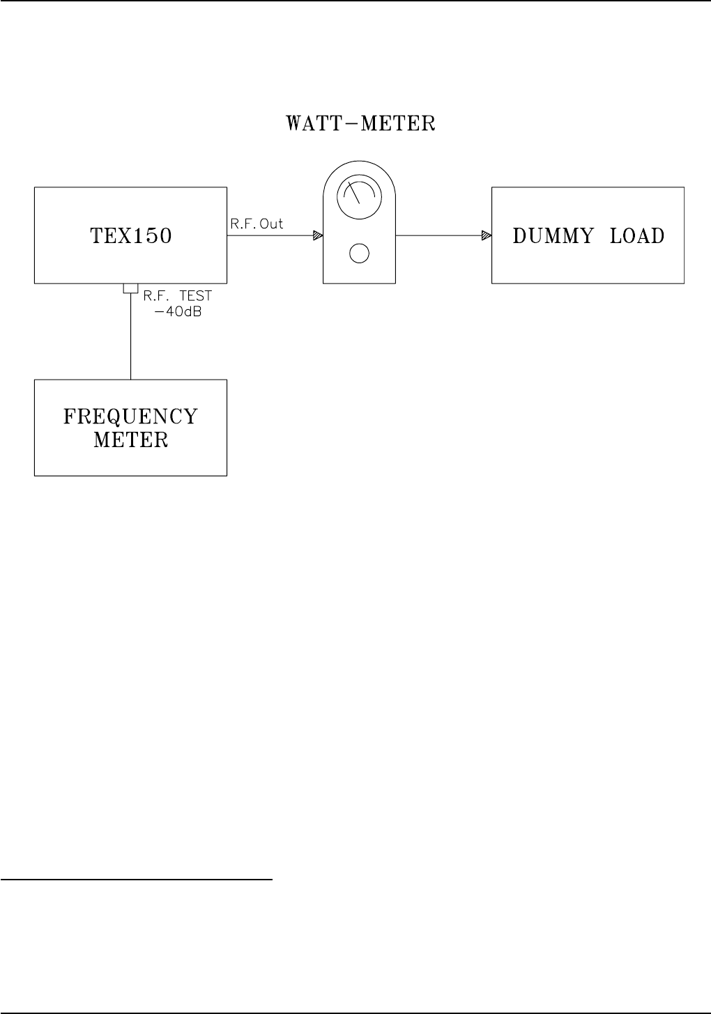
1) Switch on the equipment and select the frequency of 98MHz.
2)Wait 10 minutes to have thermal stabilization of the equipment.
3)Unscrew the fixing screws of PLL's metal box and open the cover near
to VCO metal box.
4)Check with frequency meter if the frequency setted is right. If the
frequency read on frequency meter is different from frequency setted
on the contraves , adjust variable capacitor C2 on PLL card.
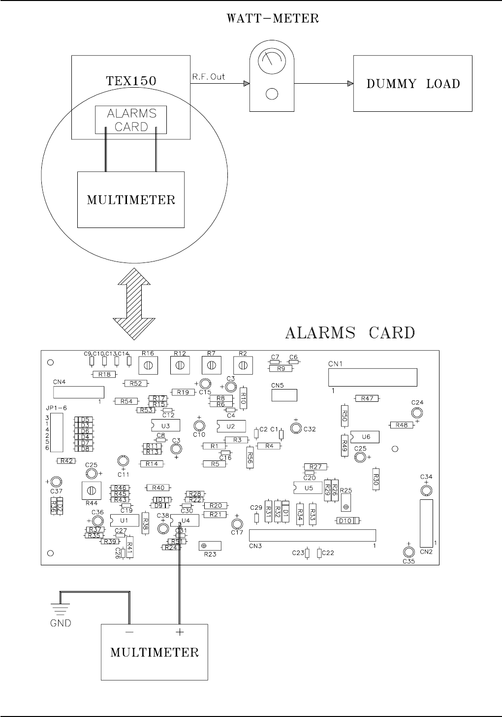
5.9 ALARMS CARD CALIBRATION5.9 ALARMS CARD CALIBRATION
5.9 ALARMS CARD CALIBRATION5.9 ALARMS CARD CALIBRATION
5.9 ALARMS CARD CALIBRATION
After having replaced the alarms card, carry out the following
procedure:
A) Internal AGC Adjustment
1)Connect a 50 Ohm, 300 W dummy load to the RF output.
2)Adjust output power at minimum turning PWR ADJ trimmer (9 Fig.1a or
5 Fig.1B) completely anticlockwise and then switch on the equipment.

XT150 and XT150S Technical and Maintenance Manual
Pag. 41
3)Turn trimmer R2, placed on Alarms card, completely clockwise.
4)Increase output power until maximum through PWR ADJ (9 Fig.1A or 5
Fig.1B) trimmer (clockwise).
5)Adjust variable capacitor C2 on Directional Coupler to read, through
a voltmeter between Directional Coupler's REF contact and GND (see
as reference Directional Coupler Layout), minimum voltage value.
6)Adjust R2 to obtain a reading of 150W on external wattmeter.
7)Select with Meter Selector (11 Fig.1A or 8 Fig.1B) the FWD position.
8)Adjust trimmer R8 on METER card to read 150W on TEX150's analog meter.
B) Internal VSWR Adjustment
1)Connect a 50 Ohm, 300 W dummy load to the RF output.
2)Adjust output power at minimum turning PWR ADJ trimmer (9 Fig.1A or
5 Fig.1B) completely anticlockwise and then switch on the equipment.
3)Turn trimmer R7, placed on Alarms card, completely clockwise.
4)Disconnect external dummy load, increase output power until 150W
turning PWR ADJ trimmer (9 Fig.1 or 5 Fig.2) clockwise. Output
power must increase slowly because the protection is working.(If this
doesn't happen, suspend all operation e contact the seller)
5)Adjust R7 to obtain a reading of 10W on external wattmeter.
6)Select with Meter Selector (11 Fig.1A or 8 Fig.1B) the REF position.
7)Adjust trimmer R7 on METER card to read 10W on TEX150's analog
meter.
XT150 and XT150S Technical and Maintenance Manual
Pag. 42
C) External AGC Adjustment
1)Perform SETUP 9 (A and B).
SETUP 9ASETUP 9A
SETUP 9ASETUP 9A
SETUP 9A
SETUP 9BSETUP 9B
SETUP 9BSETUP 9B
SETUP 9B
2)Adjust output power at minimum turning PWR ADJ trimmer (9 Fig.1 or
5 fig.2) completely anticlockwise and then switch on the equipment.
3)This adjustment it's necessary when TEX150 is connected as exciter
or driver for a power amplifier. Therefore, it's necessary to have on
last amplifier of the system an output voltage proportional with antenna
output forward power and connect this signal to REMOTE1 (3 Fig.2).
Increase TEX150's output power with PWR ADJ (9 Fig.1) to have the
necessary output power to drive the next stage of the system (e.g. for
a 1KW amplifier, read 1050W on external wattmeter).
4)Turn trimmer R16, until to have maximum output power of the power
amplifier on external wattmeter (e.g. 1000W). In these conditions is
possible to control output power into the range of 50W presetted,protecting
the equimpment against voltage variations).
D) External VSWR Adjustment
1)Perform SETUP 10.
SETUP 10SETUP 10
SETUP 10SETUP 10
SETUP 10

XT150 and XT150S Technical and Maintenance Manual
Pag. 43
2)Adjust output power at minimum turning PWR ADJ trimmer (9 Fig.1A
or 5 fig.1B) completely anticlockwise and then switch on the
equipment.
3)This adjustment it's necessary when TEX150 is connected as exciter
or driver for a power amplifier. Therefore, it's necessary to have
on last amplifier of the system an output voltage proportional with
antenna output reflected power and connect this signal to RE-
MOTE2 (6 Fig.2).
4)Turn trimmer R12, until to have an output power of the power
amplifier on external wattmeter (e.g. 900W, -10%).
In these conditions is possible to control output power into the range
of ±10% presetted, protecting the equimpment against VSWR varia-
tions).
E) Temperature Alarm Adjustment
1)Perform SETUP 11.
2)Adjust output power at minimum turning PWR ADJ trimmer (9 Fig.1A
or 5 fig.1B) completely anticlockwise and then switch on the
equipment.
3)Increase output power until 150W turning PWR ADJ trimmer (9 Fig.1A
or 5 Fig.1B) clockwise.
4)Turn trimmer R23, until to have on pin 3 of U4 a voltage included
between 265 and 275 mV. In these conditions temperature protection
starts at 70°C. Adjust R23 until output power begins to decrease.
5)Then, adjust R25 until SWR/TEMP led indicator (8 Fig.1A or 4 Fig.1B)
starts to blink.
XT150 and XT150S Technical and Maintenance Manual
Pag. 44
SETUP 11

XT150 and XT150S Technical and Maintenance Manual
Pag. 45
F) Maximum Output Power Adjustment
Can be necessary to set maximum output power at maximum value included
between 10 and 150W.
1)Connect a 50 ohm, 300W dummy load to the RF output.
2)Adjust output power at minimum turning PWR ADJ trimmer (9 Fig.1A
or 5 Fig.1B) completely anticlockwise and then switch on the
equipment.
3)Increase output power until 150W turning PWR ADJ trimmer
(9 Fig.1A or 5 Fig.1B) clockwise.
4)Turn trimmer R44, until to have maximum output power presetted on
external wattmeter.
5)Then, adjust output power turning PWR ADJ trimmer (9 Fig.1A or 5
fig.1B) and note that output power can be increased over presetted value.
NOTE: The jumpers shown in table , disable all protections (all enabled
from firm). A no-correct use of these jumpers can cause seroius damage
to the unit and will automatically make the warranty void.
ALARMS CARD TRIMMERS AND JUMPERSALARMS CARD TRIMMERS AND JUMPERS
ALARMS CARD TRIMMERS AND JUMPERSALARMS CARD TRIMMERS AND JUMPERS
ALARMS CARD TRIMMERS AND JUMPERS
REF.REF.
REF.REF.
REF. DESCRIPTIONDESCRIPTION
DESCRIPTIONDESCRIPTION
DESCRIPTION
R2 Internal AGC Adjustment
R7 Max Power Output Adjustment (VSWR INFINITE)
R12 External VSWR Threshold Adjustment
R16 External AGC Adjustment
R23 Temperature Threshold Adjustment
R25 Temperature Led Lighting Adjustment
R44 Max Power Output Adjustment
JP1 Internal AGC Insertion (DON'T REMOVE)
JP2 Internal AGC Insertion (DON'T REMOVE)
JP3 External VSWR Insertion
JP4 External AGC Insertion
JP5 Temperature Threshold Insertion
JP6 Maximum Output Power Threshold Insertion

XT150 and XT150S Technical and Maintenance Manual
Pag. 46
APPENDIX A
CIRCUIT DIAGRAMS, LAYOUTS AND BILLS OF MATERIALCIRCUIT DIAGRAMS, LAYOUTS AND BILLS OF MATERIAL
CIRCUIT DIAGRAMS, LAYOUTS AND BILLS OF MATERIALCIRCUIT DIAGRAMS, LAYOUTS AND BILLS OF MATERIAL
CIRCUIT DIAGRAMS, LAYOUTS AND BILLS OF MATERIAL
This section contains circuit diagrams, layouts and bills of
material of the modules which composing the equipment. For more
information about each module see as reference Section 2.

XT150 and XT150S Technical and Maintenance Manual
Pag. 47
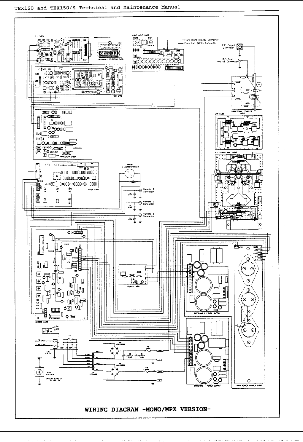
WIRING DIAGRAMWIRING DIAGRAM
WIRING DIAGRAMWIRING DIAGRAM
WIRING DIAGRAM
1 Mono/MPX Version Pag. 49
2 Stereo Version Pag. 48
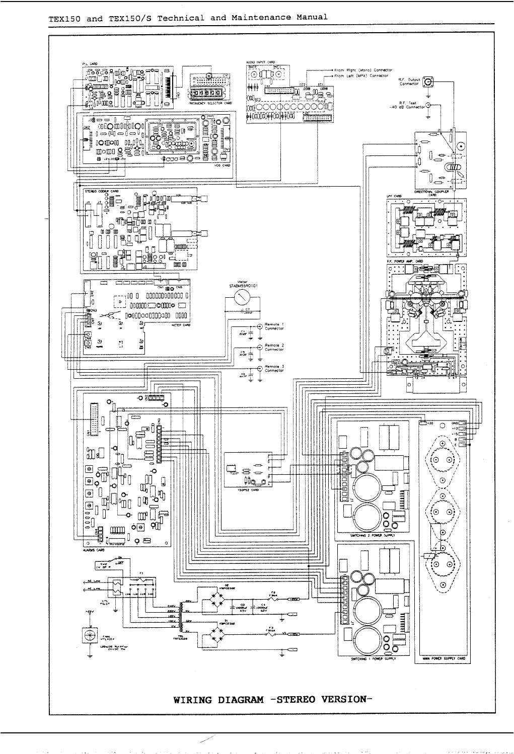
XT150 and XT150S Technical and Maintenance Manual
Pag. 48
XT150 and XT150S Technical and Maintenance Manual
Pag. 49

XT150 and XT150S Technical and Maintenance Manual
Pag. 50
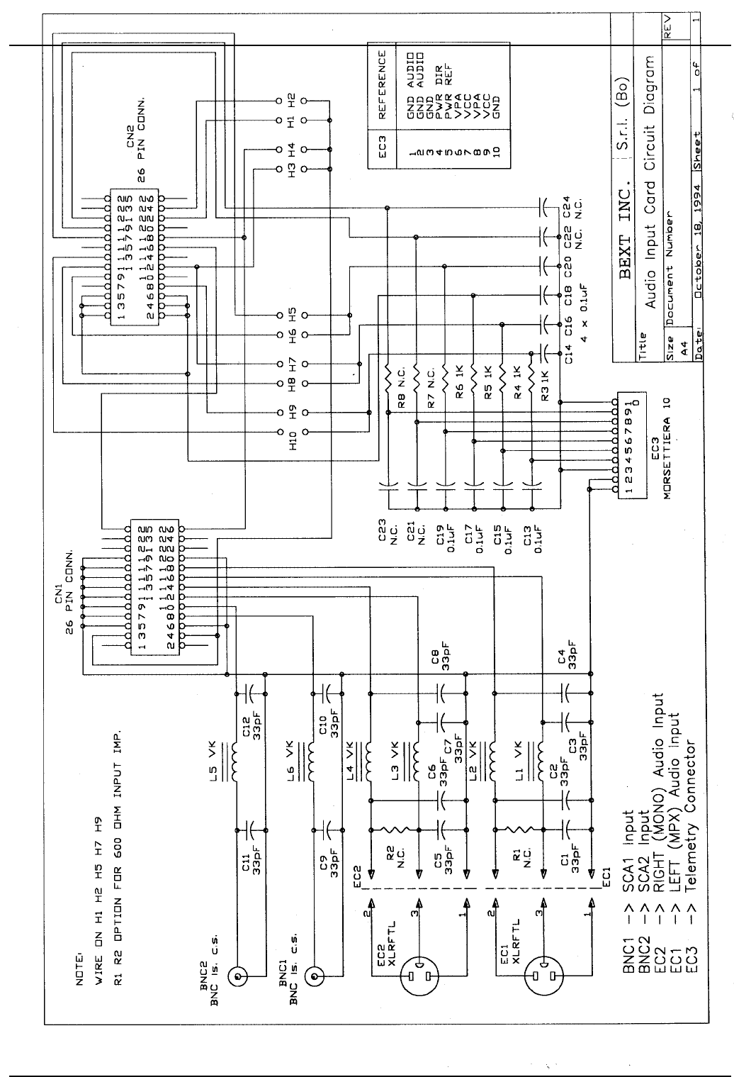
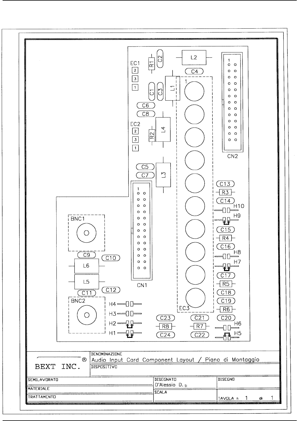
AUDIO INPUT CARDAUDIO INPUT CARD
AUDIO INPUT CARDAUDIO INPUT CARD
AUDIO INPUT CARD
1 Circuit Diagram Pag. 51
2 Bill of Materials Pag. 52
3 Component Layout Pag. 53
XT150 and XT150S Technical and Maintenance Manual
Pag. 51

XT150 and XT150S Technical and Maintenance Manual
Pag. 52
Audio Input Card Bill Of Materials Page 1
Item Quantity Reference Part Description Part Order Code
____________________________________________________________________________________________________
1 4 R3,R4, 1K RESISTOR 1/4W 5% RSC1/4JK0001
R5,R6
2 12 C1,C2,C3, 33pF CERAMIC CAPACITOR NP0 CKM330BJ600C
C4,C5,C6,
C7,C8,C9,
C10,C11,C12
3 8 C13,C14, 0.1uF CERAMIC CAPACITOR CKM104BK600P
C15,C16,
C17,C18,
C19,C20
4 6 L1,L2,L3, VK RF CHOKE IMPVK00A
L4,L5,L6
5 2 EC1,EC2 XLRFTL XLR FEMM. DA TELAIO CNTXLRFP3P
6 1 EC3 MORSET. 10 MORSETT. TEL. 10 CONT. MORSP10P
7 2 CN1,CN2 26 P CONN. CONN. M 2*13 P 2.54 CNTMCSFC26P
8 2 BNC1,BNC2 BNC IS.CS. CONN. BNC A STAMP. IS. CNTBNCFCSIS
9 10 H1,H2,H3, WIRE JUMP. PONTICELLO A FILO WIREJUMPER
H4,H5,H6,
H7,H8,
H9,H10
10 8 R1,R2,R7, N.C. NOT CONNECTED
R8,C21,C22,
C23,C24
XT150 and XT150S Technical and Maintenance Manual
Pag. 53

XT150 and XT150S Technical and Maintenance Manual
Pag. 54
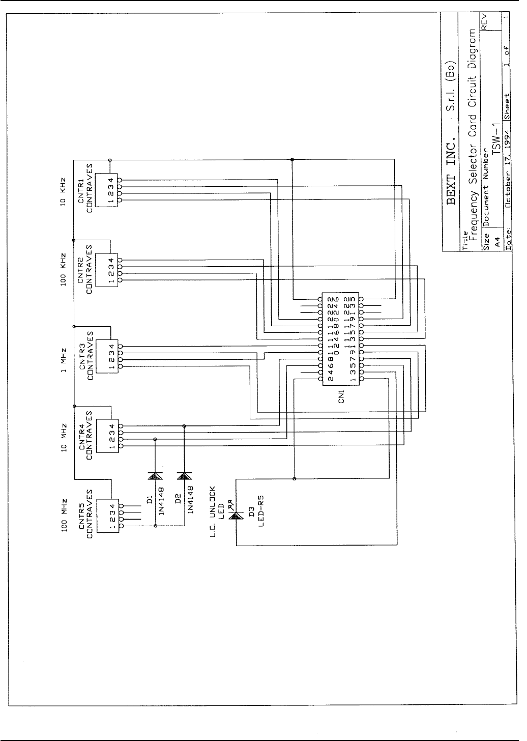
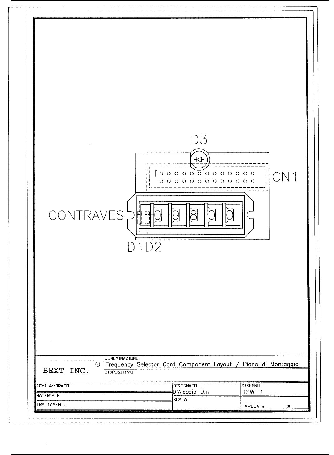
FREQUENCY SELECTOR CARD (Mod. TSW-1)FREQUENCY SELECTOR CARD (Mod. TSW-1)
FREQUENCY SELECTOR CARD (Mod. TSW-1)FREQUENCY SELECTOR CARD (Mod. TSW-1)
FREQUENCY SELECTOR CARD (Mod. TSW-1)
1 Circuit Diagram Pag. 55
2 Bill of Materials Pag. 56
3 Component Layout Pag. 57
XT150 and XT150S Technical and Maintenance Manual
Pag. 55

XT150 and XT150S Technical and Maintenance Manual
Pag. 56
Frequency Selector Card Mod. TSW-1 Bill Of Materials Page 1
Item Quantity Reference Part Description Part Order Code
____________________________________________________________________________________________________
1 1 CN1 26 P CONN. CONN. M 2*13 P 2.54 CNTMCSFC26P
2 5 CNTR1, CONTRAVES COMMUTATORI BCD 15mm COMBCD15
CNTR2,
CNTR3,
CNTR4,
CNTR5
3 2 D1,D2 1N4148 SILICON DIODE DIS1N4148
4 1 D3 LED-R5 RED LED DIODE LEDRO05
XT150 and XT150S Technical and Maintenance Manual
Pag. 57

XT150 and XT150S Technical and Maintenance Manual
Pag. 58
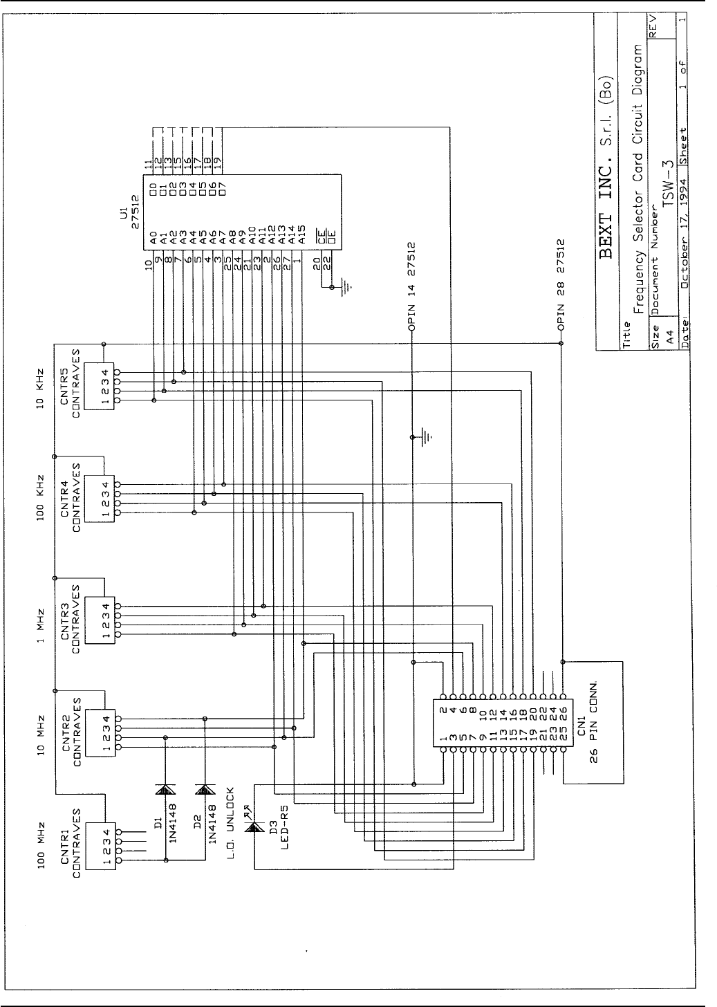
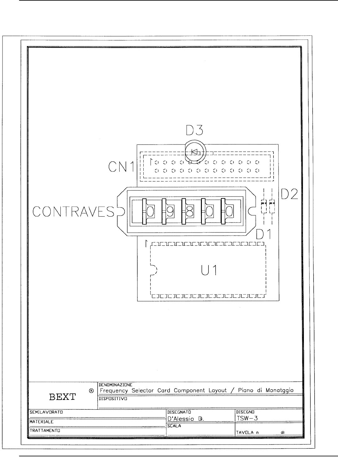
FREQUENCY SELECTOR CARD (Mod. TSW-2)FREQUENCY SELECTOR CARD (Mod. TSW-2)
FREQUENCY SELECTOR CARD (Mod. TSW-2)FREQUENCY SELECTOR CARD (Mod. TSW-2)
FREQUENCY SELECTOR CARD (Mod. TSW-2)
1 Circuit Diagram Pag. 59
2 Bill of Materials Pag. 60
3 Coponent Layout Pag. 61
XT150 and XT150S Technical and Maintenance Manual
Pag. 59

XT150 and XT150S Technical and Maintenance Manual
Pag. 60
Frequency Selector Card Mod.T SW-3 Bill Of Materials Page 1
Item Quantity Reference Part Description Part Order Code
____________________________________________________________________________________________________
1 1 CN1 26 P CONN. CONN. M 2*13 P 2.54 CNTMCSFC26P
2 5 CNTR1, CONTRAVES COMMUTATORI BCD 15mm COMBCD15
CNTR2,
CNTR3,
CNTR4,
CNTR5
3 2 D1,D2 1N4148 SILICON DIODE DIS1N4148
4 1 D3 LED-R5 RED LED DIODE LEDRO05
5 1 U1 27512 65,536x8 B CMOS EPROM CID27512
XT150 and XT150S Technical and Maintenance Manual
Pag. 61

XT150 and XT150S Technical and Maintenance Manual
Pag. 62
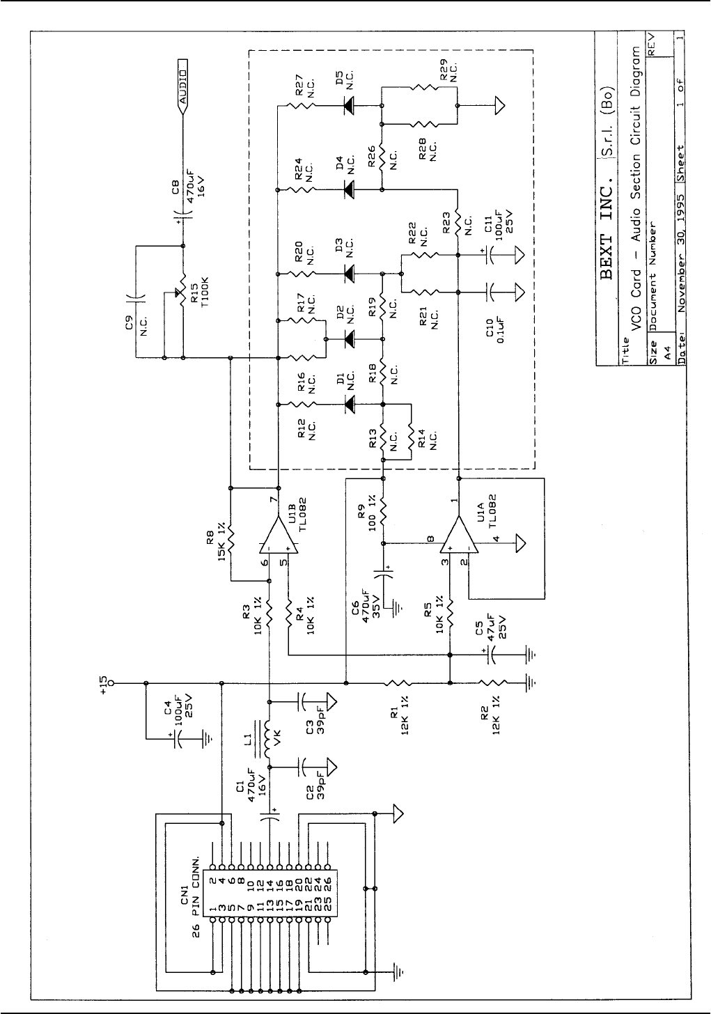
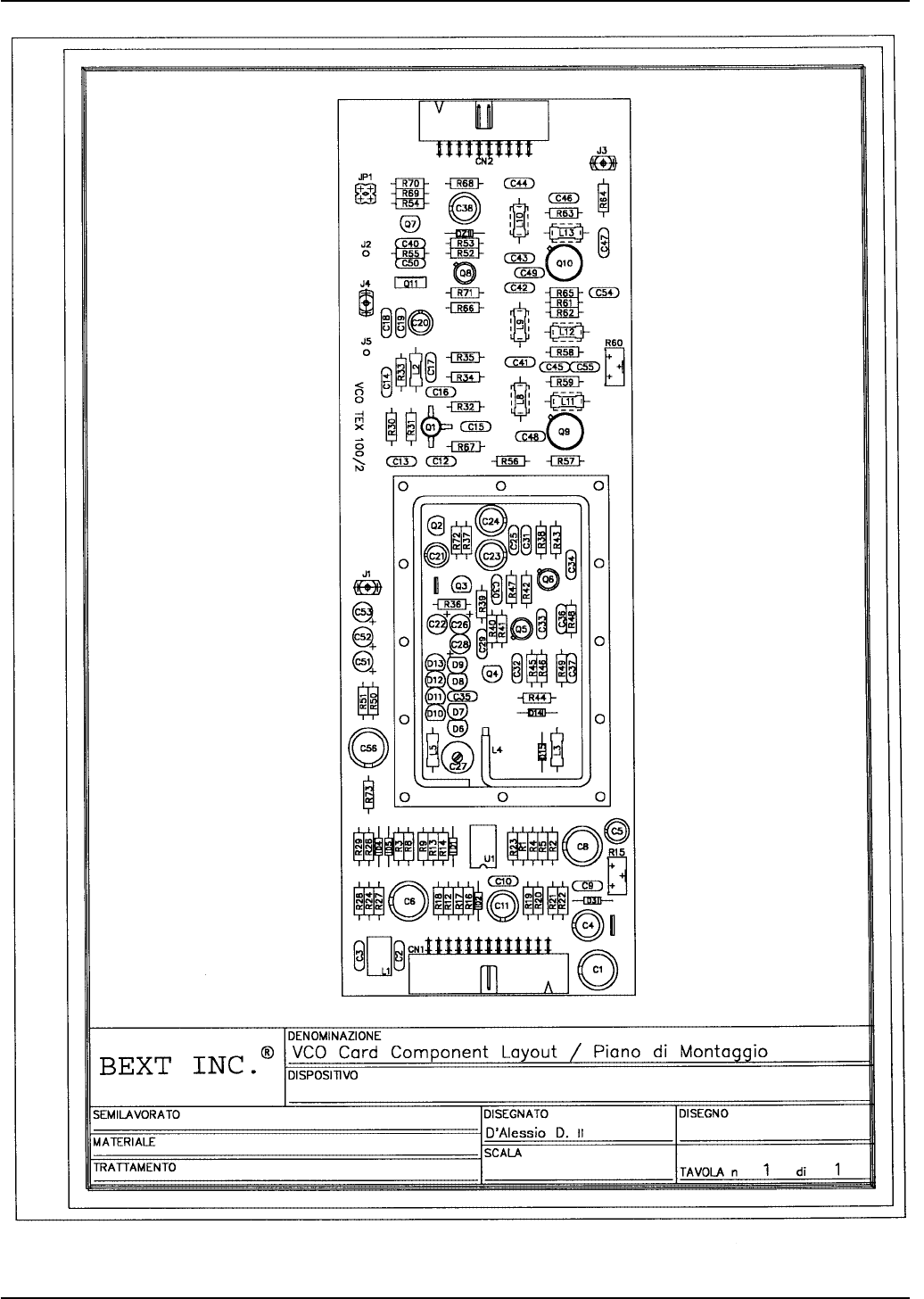
VCO CARDVCO CARD
VCO CARDVCO CARD
VCO CARD
1 A.F. Section Circuit Diagram Pag. 63
2 A.F. Section Bill of Materials Pag. 64
3 R.F. Section Circuit Diagram Pag. 65
4 R.F. Section Bill of Materials Pag. 66
5 VCO Component Layout Pag. 69
XT150 and XT150S Technical and Maintenance Manual
Pag. 63

XT150 and XT150S Technical and Maintenance Manual
Pag. 64
VCO Card - A.F. Section Bill Of Materials Page 1
Item Quantity Reference Part Description Part Order Code
____________________________________________________________________________________________________
1 1 R9 100 1% RESISTOR 1/4W 1% RSM1/4FH0100
2 3 R3,R4,R5 10K 1% RESISTOR 1/4W 1% RSM1/4FK0010
3 2 R1,R2 12K 1% RESISTOR 1/4W 1% RSM1/4FK0012
4 1 R8 15K 1% RESISTOR 1/4W 1% RSC1/4FK0015
5 1 R15 T100K TRIMMER REG. VERT. 10mm RVTD10VK0100
6 2 C2,C3 39pF CERAMIC CAPACITOR NP0 CKM390BJ600C
7 1 C10 0.1µF CERAMIC CAPACITOR CKM104BK600P
8 1 C5 47µF ELECTROLYTIC CAPACITOR CEA476BM630
9 2 C4,C11 100µF ELECTROLYTIC CAPACITOR CEA107BM350
10 3 C1,C6,C8 470µF ELECTROLYTIC CAPACITOR CEA477BM350
11 1 L1 VK RF CHOKE IMPVK00A
12 1 CN1 26P CONN. CONN. M 2*13 P 2.54 CNTMCSFC26P
13 1 U1 TL082 DOUBLE OP. AMP. CILTL082
14 22 D1,D2,D3, N.C. NOT CONNECTED
D4,D5,C9,
R12,R13,
R14,R16,
R17,R18,
R19,R20,
R21,R22,
R23,R24,
R26,R27,
R28,R29
XT150 and XT150S Technical and Maintenance Manual
Pag. 65

XT150 and XT150S Technical and Maintenance Manual
Pag. 66
VCO Card - R.F. Section Bill Of Materials Page 1
Item Quantity Reference Part Description Part Order Code
_____________________________________________________________________________________
1 1 R60 0 0 OHM RESISTOR R000
2 3 R56,R58,R64 5.6 1% RESISTOR 1/4W 1% RSM1/4FH05,6
3 4 R32,R38,5 10 1% RESISTOR 1/4W 1% RSM1/4FH0010
R48,R6
4 1 R39 22.1 1% RESISTOR 1/4W 1% RSM1/4FH22,1
5 2 R35,R59 47 1% RESISTOR 1/4W 1% RSM1/4FH0047
6 1 R34 56 1% RESISTOR 1/4W 1% RSM1/4FH0056
7 3 R33,R37,R40 100 1% RESISTOR 1/4W 1% RSM1/4FH0100
8 1 R73 120 1% RESISTOR 1/4W 1% RSM1/4FH0120
9 1 R63 210 1% RESISTOR 1/4W 1% RSM1/4FH0210
10 1 R43 220 1% RESISTOR 1/4W 1% RSM1/4FH0220
11 1 R62 270 1% RESISTOR 1/4W 1% RSM1/4FH0270
12 2 R44,R46 470 1% RESISTOR 1/4W 1% RSM1/4FH0470
13 2 R36,R49 680 1% RESISTOR 1/4W 1% RSM1/4FH0680
14 4 R50,R67, 1K 1% RESISTOR 1/4W 1% RSM1/4FK0001
R68,R71
15 1 R61 1K5 1% RESISTOR 1/4W 1% RSC1/4FK01,5
16 1 R45 2K7 1% RESISTOR 1/4W 1% RSM1/4FK02,8
17 2 R42,R55 4K7 1% RESISTOR 1/4W 1% RSM1/4FK04,7
18 1 R57 5K6 1% RESISTOR 1/4W 1% RSM1/4FK05,6
19 1 R47 6K8 1% RESISTOR 1/4W 1% RSM1/4FK06,8
20 5 R41,R51, 10K 1% RESISTOR 1/4W 1% RSM1/4FK0010
R66,R69,R72
21 2 R31,R54 22K 1% RESISTOR 1/4W 1% RSM1/4FK0022
22 1 R53 47K 1% RESISTOR 1/4W 1% RSM1/4FK0047
23 1 R52 1M 1% RESISTOR 1/4W 1% RSM1/4FM0001
24 1 C16 2p2 CERAMIC CAPACITOR NP0 CKM2,2BJ600C
25 1 C35 22pF CERAMIC CAPACITOR NP0 CKM220BJ600C
26 1 C32 33pF CERAMIC CAPACITOR NP0 CKM330BJ600C
XT150 and XT150S Technical and Maintenance Manual
Pag. 67

XT150 and XT150S Technical and Maintenance Manual
Pag. 68
VCO Card - R.F. Section Bill Of Materials Page 3
Item Quantity Reference Part Description Part Order Code
____________________________________________________________________________________________________
53 1 Q4 J310 FET TRANSISTOR TRNJ310
54 7 JP1,C13, N.C. NOT CONNECTED
C27,R30,
C51,C53,R70
55 2 C34,C36 100pF CERAMIC CAPACITOR NP0 CKM101BJ600C
56 1 C12 220pF CERAMIC CAPACITOR NP0 CKM221BK600C
XT150 and XT150S Technical and Maintenance Manual
Pag. 69

XT150 and XT150S Technical and Maintenance Manual
Pag. 70
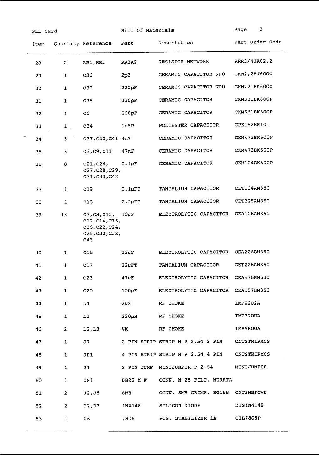
PLL CARDPLL CARD
PLL CARDPLL CARD
PLL CARD
1 Circuit Diagram Pag. 71
2 Bill of Materials Pag. 72
3 Coponent Layout Pag. 77
XT150 and XT150S Technical and Maintenance Manual
Pag. 71

XT150 and XT150S Technical and Maintenance Manual
Pag. 72
PLL Card Bill Of Materials Page 1
Item Quantity Reference Part Description Part Order Code
____________________________________________________________________________________________________
1 1 R49 0 0 OHM RESISTOR R000
2 1 R43 10 1% RESISTOR 1/4W 1% RSM1/4FH0010
3 1 R39 22 1% RESISTOR 1/4W 1% RSM1/4FH0022
4 1 R22 27 1% RESISTOR 1/4W 1% RSM1/4FH0027
5 1 R42 47 1% RESISTOR 1/4W 1% RSM1/4FH0047
6 1 R41 56 1% RESISTOR 1/4W 1% RSM1/4FH0056
7 4 R5,R6,R8, 100 1% RESISTOR 1/4W 1% RSM1/4FH0100
R47
8 1 R35 180 RESISTOR 1/4W 5% RSC1/4JH0180
9 1 R44 220 1% RESISTOR 1/4W 1% RSM1/4FH0220
10 2 R32,R34 270 1% RESISTOR 1/4W 1% RSM1/4FH0270
11 1 R3 390 1% RESISTOR 1/4W 1% RSM1/4FH0390
12 4 R4,R21,R33, 470 1% RESISTOR 1/4W 1% RSM1/4FH0470
R40
13 7 R17,R18, 1K 1% RESISTOR 1/4W 1% RSM1/4FK0001
R20,R26,R27,
R30,R38
14 3 R13,R36,R37 1K5 1% RESISTOR 1/4W 1% RSC1/4FK01,5
15 1 R31 2K2 1% RESISTOR 1/4W 1% RSC1/4FK02,2
16 1 R11 4K7 1% RESISTOR 1/4W 1% RSM1/4FK04,7
17 1 R7 5K6 1% RESISTOR 1/4W 1% RSM1/4FK05,6
18 3 R9,R12,R14 10K 1% RESISTOR 1/4W 1% RSM1/4FK0010
19 2 R10,R45 22K 1% RESISTOR 1/4W 1% RSM1/4FK0022
20 1 R28 27K 1% RESISTOR 1/4W 1% RSM1/4FK0027
21 1 R48 33K 1% RESISTOR 1/4W 1% RSM1/4FK0033
22 1 R15 39K 1% RESISTOR 1/4W 1% RSM1/4FK0039
23 2 R19,R25 47K 1% RESISTOR 1/4W 1% RSM1/4FK0047
24 1 R16 82K 1% RESISTOR 1/4W 1% RSM1/4FK0082
25 1 R23 100K 1% RESISTOR 1/4W 1% RSM1/4FH0100

XT150 and XT150S Technical and Maintenance Manual
Pag. 73
PLL Card Bill Of Materials Page 2
Item Quantity Reference Part Description Part Order Code
____________________________________________________________________________________________________
26 1 R29 1M 1% RESISTOR 1/4W 1% RSM1/4FM0001
27 1 R24 10M 1% RESISTOR 1/4W 1% RSM1/4FM0010

XT150 and XT150S Technical and Maintenance Manual
Pag. 74
PLL Card Bill Of Materials Page 3
Item Quantity Reference Part Description Part Order Code
____________________________________________________________________________________________________
28 2 RR1,RR2 RR2K2 RESISTOR NETWORK RRR1/4JK02,2
29 1 C36 2p2 CERAMIC CAPACITOR NP0 CKM2,2BJ600C
30 1 C38 220pF CERAMIC CAPACITOR NP0 CKM221BK600C
31 1 C35 330pF CERAMIC CAPACITOR CKM331BK600P
32 1 C6 560pF CERAMIC CAPACITOR CKM561BK600P
33 1 C34 1n5P POLIESTER CAPACITOR CPE152BK101
34 3 C37,C40,C41 4n7 CERAMIC CAPACITOR CKM472BK600P
35 3 C3,C9,C11 47nF CERAMIC CAPACITOR CKM473BK600P
36 8 C21,C26, 0.1µF CERAMIC CAPACITOR CKM104BK600P
C27,C28,C29,
C31,C33,C42
37 1 C19 0.1µFT TANTALIUM CAPACITOR CET104AM350
38 1 C13 2.2µFT TANTALIUM CAPACITOR CET225AM350
39 13 C7,C8,C10, 10µF ELECTROLYTIC CAPACITOR CEA106AM350
C12,C14,C15,
C16,C22,C24,
C25,C30,C32,
C43
40 1 C18 22µF ELECTROLYTIC CAPACITOR CEA226BM350
41 1 C17 22µFT TANTALIUM CAPACITOR CET226AM350
42 1 C23 47µF ELECTROLYTIC CAPACITOR CEA476BM630
43 1 C20 100µF ELECTROLYTIC CAPACITOR CEA107BM350
44 1 L4 2µ2 RF CHOKE IMP02U2A
45 1 L1 220µH RF CHOKE IMP220UA
46 2 L2,L3 VK RF CHOKE IMPVK00A
47 1 J7 2 PIN STRIP STRIP M P 2.54 2 PIN CNTSTRIPMCS
48 1 JP1 4 PIN STRIP STRIP M P 2.54 4 PIN CNTSTRIPMCS
49 1 J1 2 PIN JUMP MINIJUMPER P 2.54 MINIJUMPER
50 1 CN1 DB25 M F CONN. M 25 FILT. MURATA
51 2 J2,J5 SMB CONN. SMB CRIMP. RG188 CNTSMBFCVD

XT150 and XT150S Technical and Maintenance Manual
Pag. 75
PLL Card Bill Of Materials Page 4
Item Quantity Reference Part Description Part Order Code
____________________________________________________________________________________________________
52 2 D2,D3 1N4148 SILICON DIODE DIS1N4148
53 1 U6 7805 POS. STABILIZER 1A CIL7805P

XT150 and XT150S Technical and Maintenance Manual
Pag. 76
PLL Card Bill Of Materials Page 5
Item Quantity Reference Part Description Part Order Code
____________________________________________________________________________________________________
54 1 Q3 BC547 NPN TRANSISTOR TRNBC547
55 1 Q2 2N918 NPN RF TRANSISTOR TRN2N918
56 1 Q4 BFR96 NPN RF TRANSISTOR TRNBFR96
57 1 U4 TL082 DOUBLE OP. AMP. CILTL082
58 1 U8 SP8680 ECL DIVIDER CIDSP8680B
59 1 U3 4046 CMOS PHASE COMPARATOR CID4046
60 1 U2 4518 CMOS BCD DIVIDER CID4518
61 1 U1 4520 CMOS BIN DIVIDER CID4520
62 1 U7 7400 TTL QUAD NAND CID7400
63 5 U9,U10,U11, 74LS190 TTL BCD DIVIDER CID74LS190
U12,U13
64 1 U5 74LS196 TTL LS DIVIDER CID74LS196
65 2 C39,R46 N.C. NOT CONNECTED
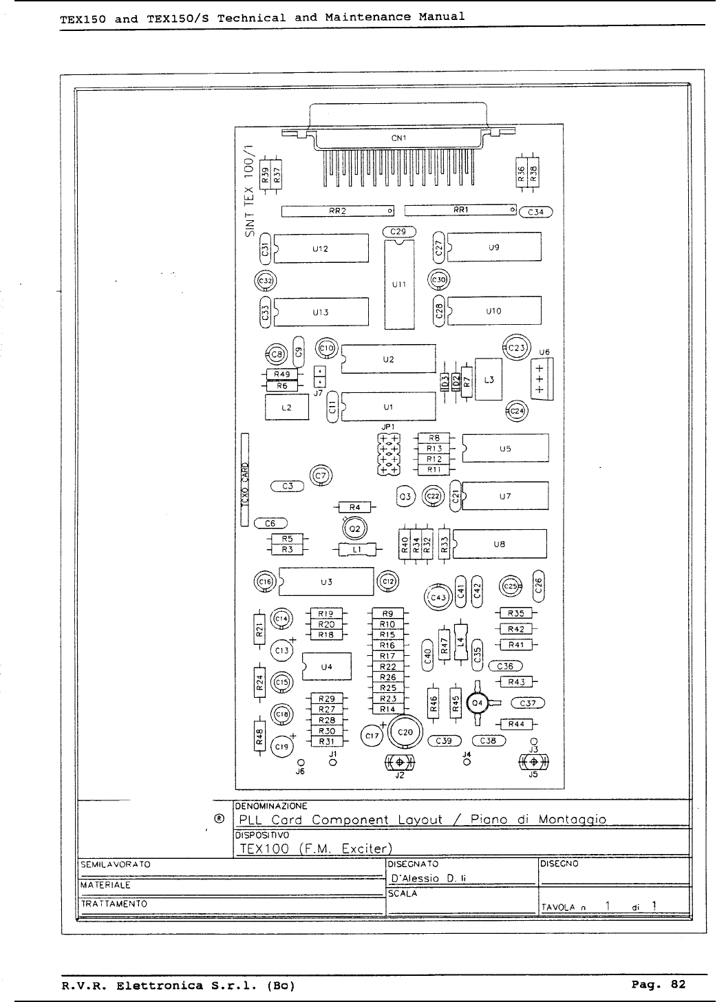
XT150 and XT150S Technical and Maintenance Manual
Pag. 77

XT150 and XT150S Technical and Maintenance Manual
Pag. 78
ALARMS CARDALARMS CARD
ALARMS CARDALARMS CARD
ALARMS CARD
1 Circuit Diagram Pag. 79
2 Bill of Materials Pag. 80
3 Coponent Layout Pag. 82
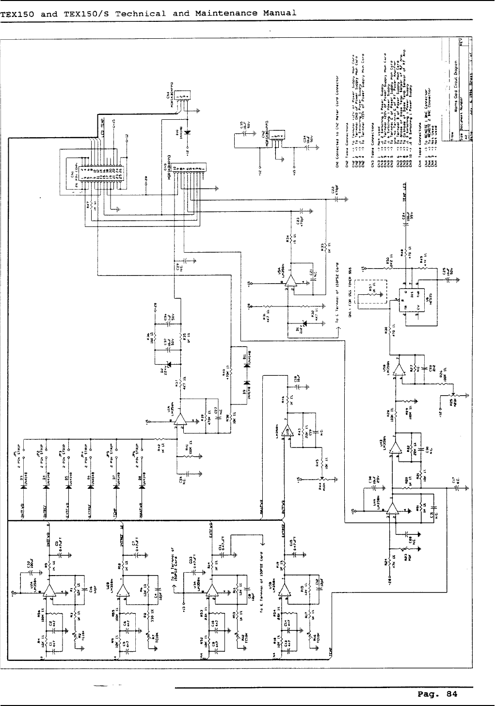
XT150 and XT150S Technical and Maintenance Manual
Pag. 79

XT150 and XT150S Technical and Maintenance Manual
Pag. 80
Alarms Card Bill Of Materials Page 1
Item Quantity Reference Part Description Part Order Code
____________________________________________________________________________________________________
1 1 R34 15 1% RESISTOR 1/4W 1% RSM1/4JH0015
2 1 R36 100 1% RESISTOR 1/4W 1% RSM1/4FH0100
3 1 R8 330 1% RESISTOR 1/4W 5% RSM1/4FH0330
4 2 R30,R48 470 1% RESISTOR 1/4W 1% RSM1/4FH0470
5 14 R3,R5,R10, 1K 1% RESISTOR 1/4W 1% RSM1/4FK0001
R13,R14,
R17,R19,
R20,R33,
R35,R42,
R46,R47,R57
6 1 R50 2K2 1% RESISTOR 1/4W 1% RSC1/4FK02,2
7 3 R31,R32,R37 4K7 1% RESISTOR 1/4W 1% RSM1/4FK04,7
8 2 R38,R45 10K 1% RESISTOR 1/4W 1% RSM1/4FK0010
9 9 R1,R4,R6, 12K 1% RESISTOR 1/4W 1% RSM1/4FK0012
R9,R11,R15,
R18,R21,R52
10 4 R22,R43, 22K 1% RESISTOR 1/4W 1% RSM1/4FK0022
R53,R54
11 2 R24,R49 47K 1% RESISTOR 1/4W 1% RSM1/4FK0047
12 6 R26,R28, 100K 1% RESISTOR 1/4W 1% RSM1/4FH0100
R29,R41,
R55,R56
13 2 R39,R40 470K 1% RESISTOR 1/4W 1% RSC1/4FK0470
14 1 R51 1M 1% RESISTOR 1/4W 1% RSM1/4FM0001
15 4 R2,R7,R12, TC10K TRIM. REG. VERT. CERMET RVTCERVK0010
R16
16 1 R23 M1K TRIMMER MULTIGIRI RVTMULAK0001
17 1 R44 M10K TRIMMER MULTIGIRI RVTMULAK0010
18 1 R25 M20K TRIMMER MULTIGIRI RVTMULAK0020
19 4 C4,C8,C12, 12pF CERAMIC CAPACITOR NP0 CKM120BJ600C
C16
20 2 C22,C23 470pF CERAMIC CAPACITOR CKM471BK600P
21 1 C20 2n2 CERAMIC CAPACITOR CKM222BK600P

XT150 and XT150S Technical and Maintenance Manual
Pag. 81
Alarms Card Bill Of Materials Page 2
Item Quantity Reference Part Description Part Order Code
____________________________________________________________________________________________________
22 8 C1,C2,C5, 4n7 CERAMIC CAPACITOR CKM472BK600P
C6,C9,C10,
C13,C14
23 5 C3,C7,C11, 0.47µFT TANTALIUM CAPACITOR CET474AM350
C15,C33
24 1 C36 1µF ELECTROLYTIC CAPACITOR CEA105AM630
25 6 C18,C25, 10µF ELECTROLYTIC CAPACITOR CEA106AM350
C34,C35,
C37,C38
26 2 C24,C32 100µF ELECTROLYTIC CAPACITOR CEA107BM350
27 6 JP1,JP2, 2 PIN STRIP STRIP M P 2.54 2 PIN CNTSTRIPMCS
JP3,JP4,
JP5,JP6
28 1 CN3 MORSKB10PPO MORS. LUMBERG F. CS 10P MORSKB10PPO
29 2 CN2,CN4 MORSKB04PPO MORS. LUMBERG F. CS 04P MORSKB04PPO
30 1 CN1 26P CONN. CONN. M 2*13 P 2.54 CNTMCSFC26P
31 9 D3,D4,D5, 1N4148 SILICON DIODE DIS1N4148
D6,D7,D8,
D9,D10,D11
32 1 D1 Z12V ZENER DIODE 12V 0.4W DIZ12V0W4
33 1 D2 Z24V ZENER DIODE 24V 0.4W DIZ24V0W4
34 5 U1,U2,U3, LM358N DOUBLE OP. AMP. CILLM358N
U4,U5
35 1 U6 NE555 TIMER CIL555
36 10 C17,C19, N.C. NOT CONNECTED
C21,C26,
R27,C27,
C28,C29,
C30,C31
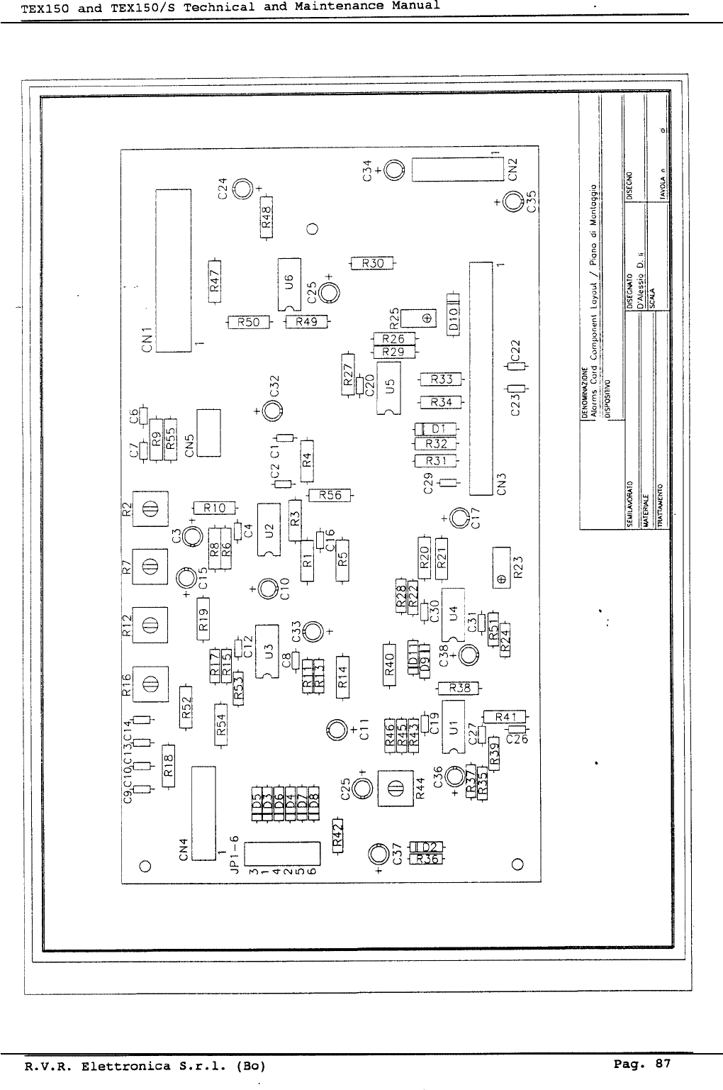
XT150 and XT150S Technical and Maintenance Manual
Pag. 82

XT150 and XT150S Technical and Maintenance Manual
Pag. 83
METER CARDMETER CARD
METER CARDMETER CARD
METER CARD
1 Circuit Diagram Pag. 84
2 Bill of Materials Pag. 85
3 Coponent Layout Pag. 87
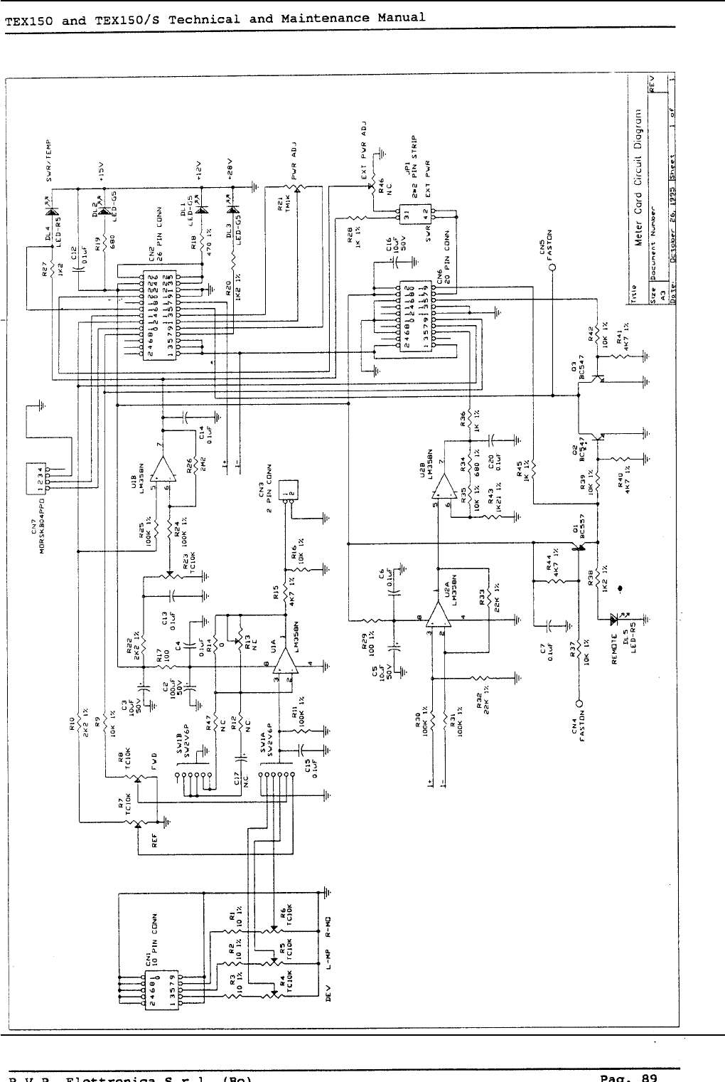
XT150 and XT150S Technical and Maintenance Manual
Pag. 84

XT150 and XT150S Technical and Maintenance Manual
Pag. 85
Meter Card Bill Of Materials Page 1
Item Quantity Reference Part Description Part Order Code
____________________________________________________________________________________________________
1 1 R14 0 0 OHM RESISTOR R000
2 3 R1,R2,R3 10 1% RESISTOR 1/4W 1% RSM1/4FH0010
3 1 R29 100 1% RESISTOR 1/4W 1% RSM1/4FH0100
4 1 R17 100 RESISTOR 1/4W 5% RSC1/4JH0100
5 1 R18 470 1% RESISTOR 1/4W 1% RSM1/4FH0470
6 1 R34 680 1% RESISTOR 1/4W 1% RSM1/4FH0680
7 1 R19 680 RESISTOR 1/4W 5% RSC1/4JH0680
8 3 R28,R36,R45 1K 1% RESISTOR 1/4W 1% RSM1/4FK0001
9 2 R20,R38 1K2 1% RESISTOR 1/4W 1% RSM1/4FK01,2
10 1 R27 1K2 RESISTOR 1/4W 5% RSC1/4JK01,2
11 1 R43 1K21 1% RESISTOR 1/4W 1% RSC1/4FK1,21
12 2 R10,R22 2K2 1% RESISTOR 1/4W 1% RSC1/4FK02,2
13 4 R15,R40, 4K7 1% RESISTOR 1/4W 1% RSM1/4FK04,7
R41,R44
14 6 R9,R16, 10K 1% RESISTOR 1/4W 1% RSM1/4FK0010
R35,R37,
R39,R42
15 2 R32,R33 22K 1% RESISTOR 1/4W 1% RSM1/4FK0022
16 5 R11,R24, 100K 1% RESISTOR 1/4W 1% RSM1/4FH0100
R25,R30,R31
17 1 R26 2M2 RESISTOR 1/4W 5% RSC1/4JM02,2
18 6 R4,R5,R6, TC10K TRIM. REG. VERT. CERMET RVTCERVK0010
R7,R8,R23
19 1 R21 TM1K TRIMM. MULT. REG. VERT. RVTMULVK0001
20 8 C4,C6,C7, 0.1µF CERAMIC CAPACITOR CKM104BK600P
C12,C13,
C14,C15,C20
21 3 C3,C5,C16 10µF ELECTROLYTIC CAPACITOR CEA106AM350
22 1 C2 100µF ELECTROLYTIC CAPACITOR CEA107BM350
23 1 JP1 2*2P STRIP STRIP M P 2.54 2*2 PIN CNTSTRIPMCS
24 2 CN4,CN5 FASTON CONN. FASTON M C.S. CNTFSTMCSGR

XT150 and XT150S Technical and Maintenance Manual
Pag. 86
Meter Card Bill Of Materials Page 2
Item Quantity Reference Part Description Part Order Code
____________________________________________________________________________________________________
25 1 CN7 MORSKB04PPO MORS. LUMB, FEMM. CS 4P MORSKB04PPO
26 1 CN3 2 PIN CONN. CONN. M 2*1 P 2.54 CNTM2PCS
27 1 CN1 10P CONN. CONN. M 2*5 P 2.54 CNTMCSFC10P
28 1 CN6 20P CONN. CONN. M 2*10 P 2.54 CNTMCSFC20P
29 1 CN2 26P CONN. CONN. M 2*13 P 2.54 CNTMCSFC26P
30 1 SW1 SW2V6P COMM.. 2 VIE 6 POS FEME COMR2V6PCS
31 2 DL4,DL5 LED-R5 RED LED DIODE LEDRO05
32 3 DL1,DL2,DL3 LED-G5 GREEN LED DIODE LEDVE05
33 2 Q2,Q3 BC547 NPN TRANSISTOR TRNBC547
34 1 Q1 BC557 PNP TRANSISTOR TRNBC557
35 2 U1,U2 LM358N DOUBLE OP. AMP. CILLM358N
36 5 R12,R13, N.C. NOT CONNECTED
C17,R46,R47
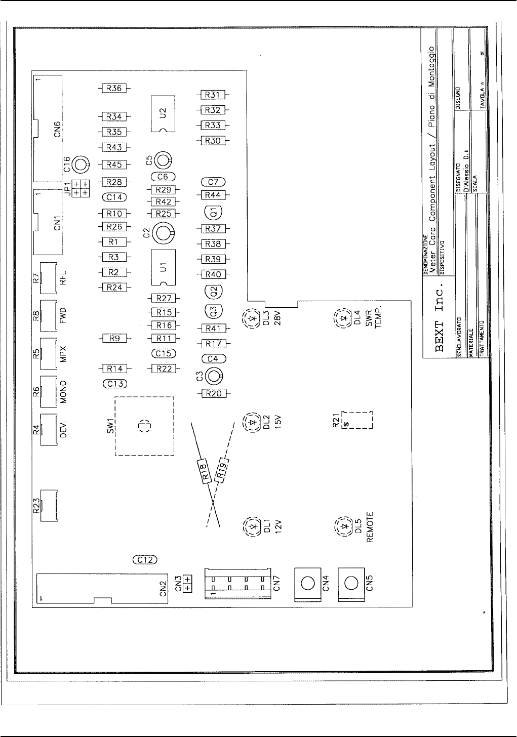
XT150 and XT150S Technical and Maintenance Manual
Pag. 87

XT150 and XT150S Technical and Maintenance Manual
Pag. 88
TRANSFORMER SUPPLY SECTIONTRANSFORMER SUPPLY SECTION
TRANSFORMER SUPPLY SECTIONTRANSFORMER SUPPLY SECTION
TRANSFORMER SUPPLY SECTION
1 Circuit Diagram Pag. 89
2 Bill of Materials Pag. 90
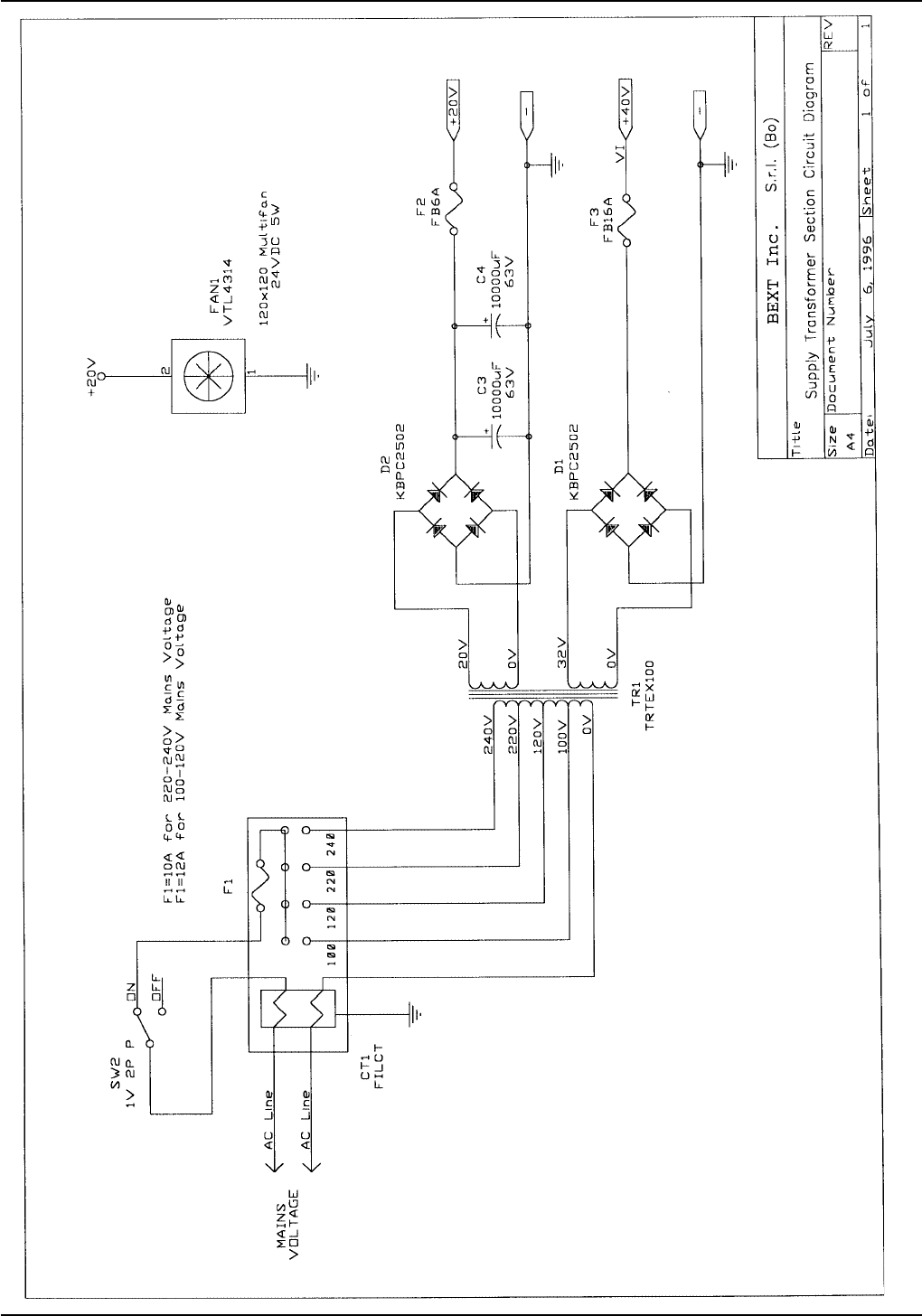
XT150 and XT150S Technical and Maintenance Manual
Pag. 89

XT150 and XT150S Technical and Maintenance Manual
Pag. 90
Transformer Supply Section Bill Of Materials Page 1
Item Quantity Reference Part Description Part Order Code
____________________________________________________________________________________________________
1 2 C3,C4 10000µF ELECTROLYTIC CAPACITOR CEA109PM630
2 1 F1 F10A FAST FUSIBILE FUS5X20RP10
3 1 F2 FB6A FAST FUSIBLE FUS6X30RP6
4 1 F3 FB16A FAST FUSIBILE FUS6X30RP16
5 1 CT1 FILCT FILTRO VDE CON C. TENS. CNTVDEMPCT
6 1 SW2 1V 2P P DEV. 1 VIA 2 POS PANN. DEV1V1103
7 2 D1,D2 KBPC2502 DIODE BRIDGE 25A PNRKBPC2502
8 1 TR1 TRTEX100 TRASFORMATORE TEX 100 TRFTEX100
9 1 FAN1 VTL4314 VENT. 120x120 24VDC 5W VTL4314

XT150 and XT150S Technical and Maintenance Manual
Pag. 91
MAIN POWER SUPPLYMAIN POWER SUPPLY
MAIN POWER SUPPLYMAIN POWER SUPPLY
MAIN POWER SUPPLY
1 Circuit Diagram Pag. 92
2 Bill of Materials Pag. 93
3 Coponent Layout Pag. 94
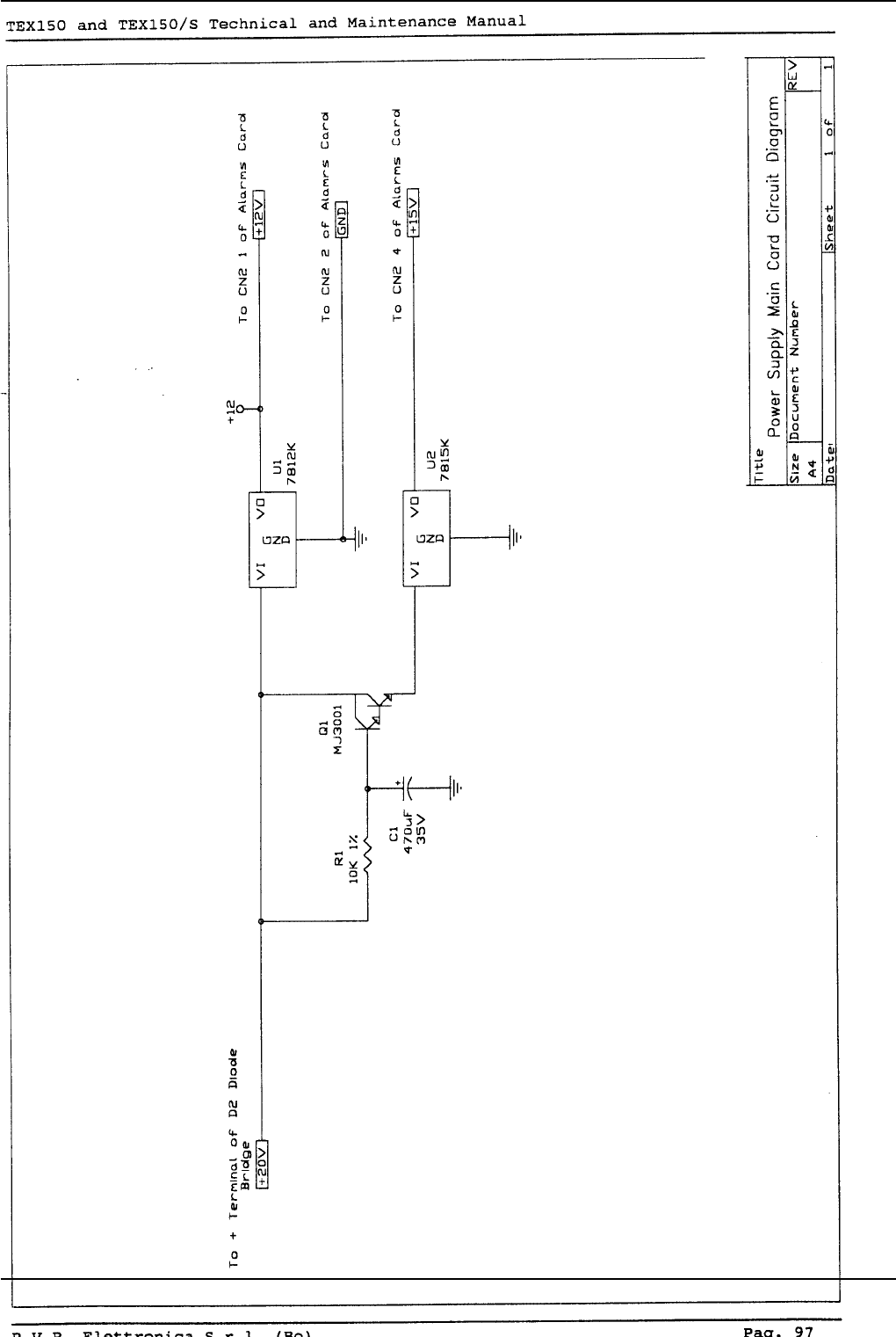
XT150 and XT150S Technical and Maintenance Manual
Pag. 92

XT150 and XT150S Technical and Maintenance Manual
Pag. 93
Main Power Supply Bill Of Materials Page 1
Item Quantity Reference Part Description Part Order Code
____________________________________________________________________________________________________
1 1 R1 10K 1% RESISTOR 1/4W 1% RSM1/4FK0010
2 1 C1 470µF ELECTROLYTIC CAPACITOR CEA477BM350
3 1 U1 7812K POS. STABILIZER 1.5A CIL7812K
4 1 U2 7815K POS. STABILIZER 1.5A CIL7815K
5 1 Q1 MJ3001 POWER TRANSISTOR TRNMJ3001
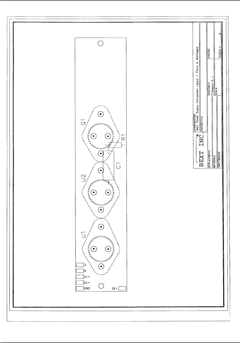
XT150 and XT150S Technical and Maintenance Manual
Pag. 94

XT150 and XT150S Technical and Maintenance Manual
Pag. 95
SWITCHING 1 POWER SUPPLYSWITCHING 1 POWER SUPPLY
SWITCHING 1 POWER SUPPLYSWITCHING 1 POWER SUPPLY
SWITCHING 1 POWER SUPPLY
1 Circuit Diagram Pag. 96
2 Bill of Materials Pag. 97
3 Coponent Layout Pag. 98
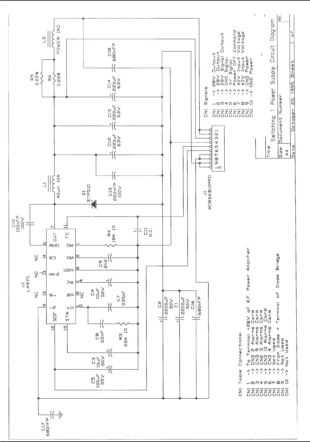
XT150 and XT150S Technical and Maintenance Manual
Pag. 96

XT150 and XT150S Technical and Maintenance Manual
Pag. 97
Switching 1 Power Supply Bill Of Materials Page 1
Item Quantity Reference Part Description Part Order Code
____________________________________________________________________________________________________
1 2 R5,R6 0.22$ RESISTOR 5W RAF005JH0,22
2 1 R4 18K 1% RESISTOR 1/4W 1% RSM1/4FK0018
3 1 R3 22K 1% RESISTOR 1/4W 1% RSM1/4FK0022
4 1 C7 330pF CERAMIC CAPACITOR CKM331BK600P
5 1 C9 2n2 CERAMIC CAPACITOR CKM222BK600P
6 1 C8 22nF CERAMIC CAPACITOR CKM223BK600P
7 1 C10 100nFP POLIESTER CAPACITOR CPE104DK101
8 1 C15 220nFP POLIESTER CAPACITOR CPE224DK101
9 3 C16,C17,C18 680nFP POLIESTER CAPACITOR CPE684DK101
10 2 C3,C4 10µF ELECTROLYTIC CAPACITOR CEA106AM350
11 1 C5 100µF ELECTROLYTIC CAPACITOR CEA107BM350
12 3 C12,C13,C14 220µF ELECTROLYTIC CAPACITOR CEA227BM350
13 2 C1,C2 2200µF ELECTROLYTIC CAPACITOR CEA228CM350
14 1 L1 40µH 10A TOROIDAL RF CHOKE 10A IMP40U10A
15 1 L2 POWER IND. RF BINOC. CHOCKE
16 1 J1 MORSKB10PPO MORS. LUMBERG F. CS 10P MORSKB10PPO
17 1 D1 STPS10 RECTIFIER DIODE DIDSTPS10
18 1 U1 L4970 SWITCHING REGULATOR CILL4970
19 1 C11 N.C. NOT CONNECTED
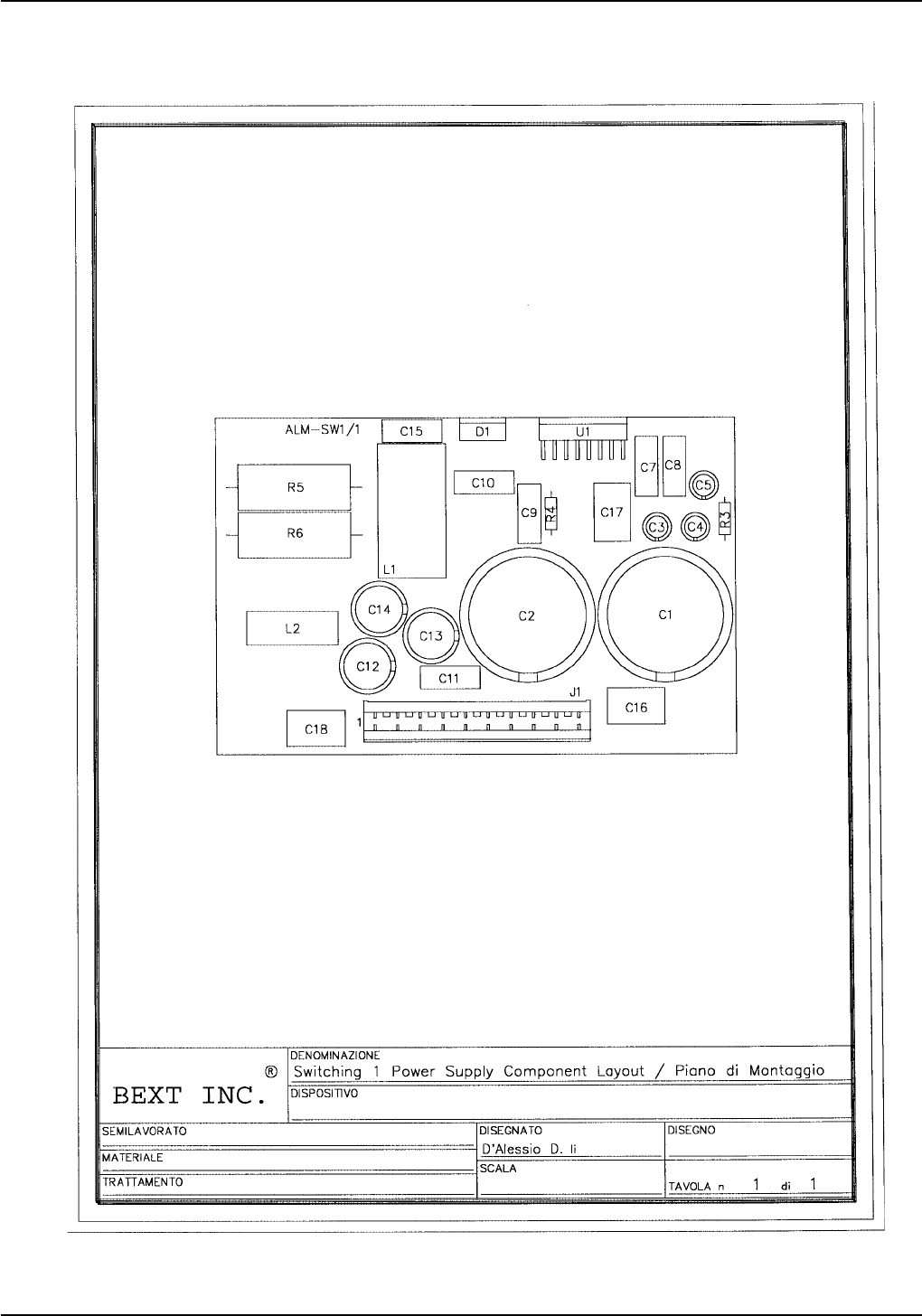
XT150 and XT150S Technical and Maintenance Manual
Pag. 98

XT150 and XT150S Technical and Maintenance Manual
Pag. 99
SWITCHING 2 POWER SUPPLYSWITCHING 2 POWER SUPPLY
SWITCHING 2 POWER SUPPLYSWITCHING 2 POWER SUPPLY
SWITCHING 2 POWER SUPPLY
1 Circuit Diagram Pag. 100
2 Bill of Materials Pag. 101
3 Coponent Layout Pag. 102
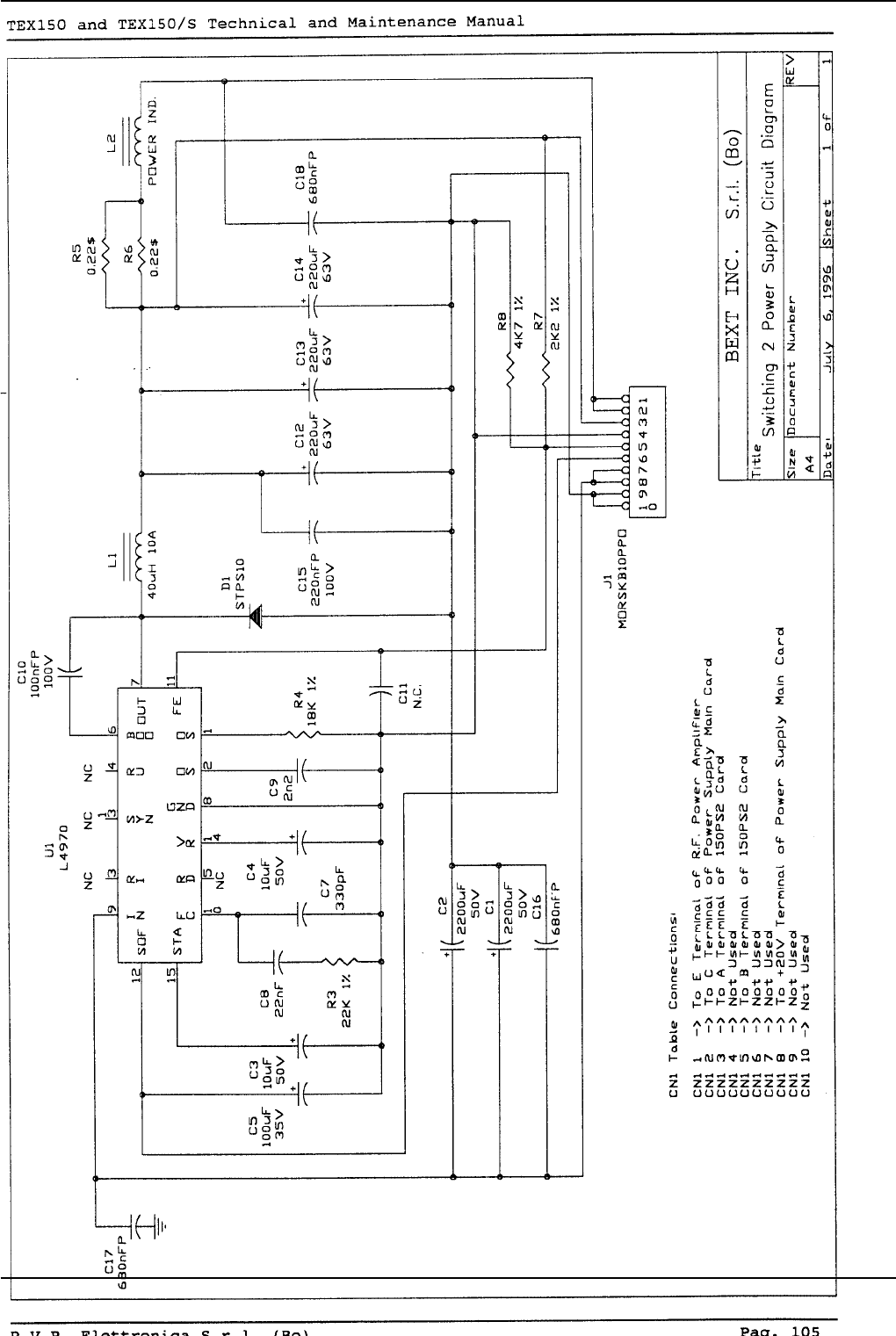
XT150 and XT150S Technical and Maintenance Manual
Pag. 100

XT150 and XT150S Technical and Maintenance Manual
Pag. 101
Switching 2 Power Supply Bill Of Materials Page 1
Item Quantity Reference Part Description Part Order Code
____________________________________________________________________________________________________
1 2 R5,R6 0.22$ RESISTOR 5W RAF005JH0,22
2 1 R7 2K2 1% RESISTOR 1/4W 1% RSC1/4FK02,2
3 1 R8 4K7 1% RESISTOR 1/4W 1% RSM1/4FK04,7
4 1 R4 18K 1% RESISTOR 1/4W 1% RSM1/4FK0018
5 1 R3 22K 1% RESISTOR 1/4W 1% RSM1/4FK0022
6 1 C7 330pF CERAMIC CAPACITOR CKM331BK600P
7 1 C9 2n2 CERAMIC CAPACITOR CKM222BK600P
8 1 C8 22nF CERAMIC CAPACITOR CKM223BK600P
9 1 C10 100nFP POLIESTER CAPACITOR CPE104DK101
10 1 C15 220nFP POLIESTER CAPACITOR CPE224DK101
11 3 C16,C17,C18 680nFP POLIESTER CAPACITOR CPE684DK101
12 2 C3,C4 10µF ELECTROLYTIC CAPACITOR CEA106AM350
13 1 C5 100µF ELECTROLYTIC CAPACITOR CEA107BM350
14 3 C12,C13,C14 220µF ELECTROLYTIC CAPACITOR CEA227BM350
15 2 C1,C2 2200µF ELECTROLYTIC CAPACITOR CEA228CM350
16 1 L1 40µH 10A TOROIDAL RF CHOKE 10A IMP40U10A
17 1 L2 POWER IND. RF BINOC. CHOCKE
18 1 J1 MORSKB10PPO MORS. LUMBERG F. CS 10P MORSKB10PPO
19 1 D1 STPS10 RECTIFIER DIODE DIDSTPS10
20 1 U1 L4970 SWITCHING REGULATOR CILL4970
21 1 C11 N.C. NOT CONNECTED
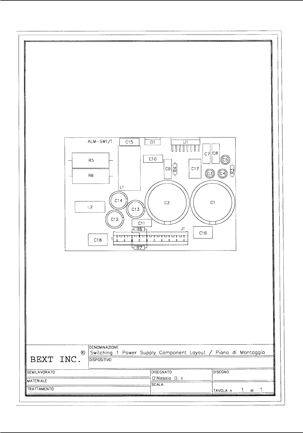
XT150 and XT150S Technical and Maintenance Manual
Pag. 102

XT150 and XT150S Technical and Maintenance Manual
Pag. 103
MONO/MPX CARDMONO/MPX CARD
MONO/MPX CARDMONO/MPX CARD
MONO/MPX CARD
1 Circuit Diagram Pag. 104
2 Bill of Materials Pag. 105
3 Coponent Layout Pag. 108
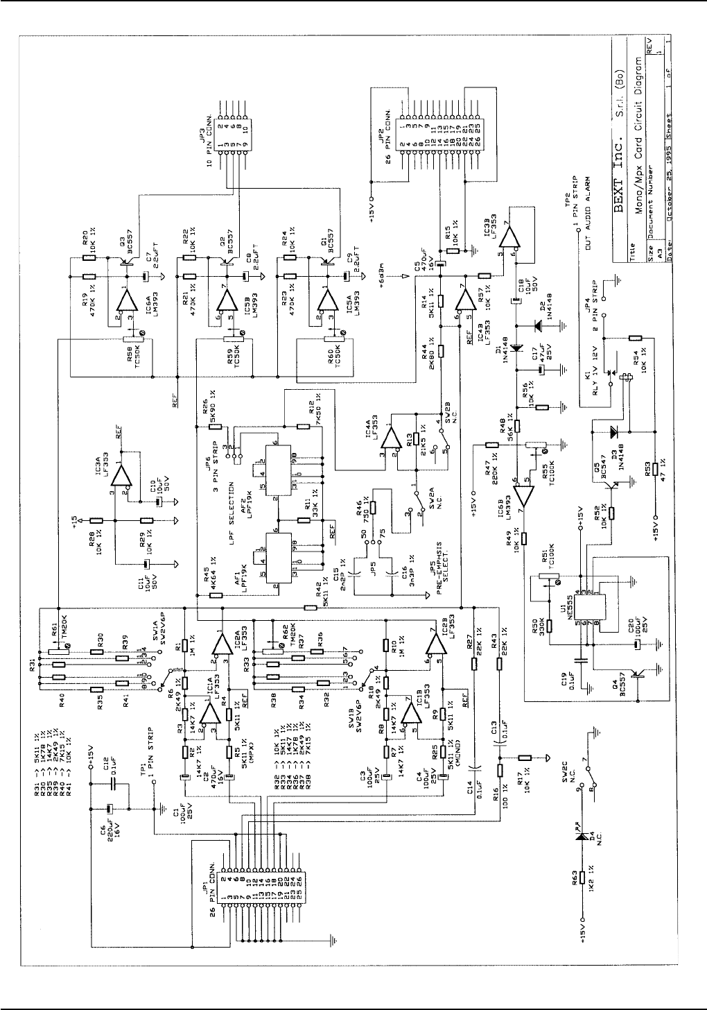
XT150 and XT150S Technical and Maintenance Manual
Pag. 104

XT150 and XT150S Technical and Maintenance Manual
Pag. 105
Mono/MPX Card Bill Of Materials Page 1
Item Quantity Reference Part Description Part Order Code
____________________________________________________________________________________________________
1 1 R53 47 1% RESISTOR 1/4W 1% RSM1/4FH0047
2 1 R16 100 1% RESISTOR 1/4W 1% RSM1/4FH0100
3 1 R46 750 1% RESISTOR 1/4W 1% RSM1/4FH0750
4 1 R63 1K2 1% RESISTOR 1/4W 1% RSM1/4FK01,2
5 2 R30,R36 1K78 1% RESISTOR 1/4W 1% RSM1/4FK1,78
6 4 R6,R18, 2K49 1% RESISTOR 1/4W 1% RSM1/4FK2,49
R37,R39
7 1 R44 2K80 1% RESISTOR 1/4W 1% RSM1/4FK2,80
8 1 R45 4K64 1% RESISTOR 1/4W 1% RSM1/4FK4,64
9 8 R4,R5,R9, 5K11 1% RESISTOR 1/4W 1% RSM1/4FK5,11
R14,R25,
R31,R33,R42
10 1 R26 5K90 1% RESISTOR 1/4W 1% RSM1/4FK5,90
11 2 R38,R40 7K15 1% RESISTOR 1/4W 1% RSM1/4FK7,15
12 1 R12 7K50 1% RESISTOR 1/4W 1% RSM1/4FK7,50
13 14 R15,R17, 10K 1% RESISTOR 1/4W 1% RSM1/4FK0010
R20,R22,
R24,R28,
R29,R32,
R41,R49,
R52,R54,
R56,R57
14 6 R2,R3,R7, 14K7 1% RESISTOR 1/4W 1% RSM1/4FK14,7
R8,R34,R35
15 1 R13 21K5 1% RESISTOR 1/4W 1% RSM1/4FK21,5
16 2 R27,R43 22K 1% RESISTOR 1/4W 1% RSM1/4FK0022
17 1 R11 33K 1% RESISTOR 1/4W 1% RSM1/4FK0033
18 1 R48 56K 1% RESISTOR 1/4W 1% RSM1/4FK0056
19 1 R47 220K 1% RESISTOR 1/4W 1% RSM1/4FK0220
20 1 R50 330K RESISTOR 1/4W 5% RSC1/4JK0330
21 3 R19,R21,R23 470K 1% RESISTOR 1/4W 1% RSC1/4FK0470
22 2 R1,R10 1M 1% RESISTOR 1/4W 1% RSM1/4FM0001

XT150 and XT150S Technical and Maintenance Manual
Pag. 106
Mono/MPX Card Bill Of Materials Page 2
Item Quantity Reference Part Description Part Order Code
____________________________________________________________________________________________________
23 3 R58,R59,R60 TC50K TRIM. REG. VERT. CERMET RVTCERVK0050
24 2 R51,R55 TC100K TRIM. REG. VERT. CERMET RVTCERVK0100
25 2 R61,R62 TM20K TRIM. MULT. REG. VERT. RVTMULVK0020
26 1 C15 2n2P 1% POLIESTER CAPACITOR CPE222BF63
27 1 C16 3n3P 1% POLIESTER CAPACITOR 1% CPE332BF101
28 4 C12,C13, 0.1µF CERAMIC CAPACITOR CKM104BK600P
29 3 C7,C8,C9 2.2µFT TANTALIUM CAPACITOR CET225AM350
30 3 C10,C11,C18 10µF ELECTROLYTIC CAPACITOR CEA106AM350
31 1 C17 47µF ELECTROLYTIC CAPACITOR CEA476BM630
32 4 C1,C3,C4, 100µF ELECTROLYTIC CAPACITOR CEA107BM350
C20
33 1 C6 220µF ELECTROLYTIC CAPACITOR CEA227BM350
34 2 C2,C5 470µF ELECTROLYTIC CAPACITOR CEA477BM350
35 2 AF1,AF2 LPF19K 19KHZ LOW PASS FILTER FLP19KHZ
36 2 TP1,TP2 1 PIN STRIP STRIP M 1 PIN CNTSTRIPMCS
37 1 JP4 2 PIN STRIP STRIP M P 2.54 2 PIN CNTSTRIPMCS
38 2 JP5,JP6 3 PIN STRIP STRIP M P 2.54 3 PIN CNTSTRIPMCS
39 1 JP3 10P CONN. CONN. M 2*5 P 2.54 CNTMCSFC10P
40 2 JP1,JP2 26P CONN. CONN. M 2*13 P 2.54 CNTMCSFC26P
41 1 K1 RLY 1V 12V RELAY 1 VIA 12V RLD112
42 1 SW1 SW2V6P COMM. 2 VIE 6 POS FEME COMR2V6PCS
43 3 D1,D2,D3 1N4148 SILICON DIODE DIS1N4148
44 1 Q5 BC547 NPN TRANSISTOR TRNBC547
45 4 Q1,Q2,Q3,Q4 BC557 PNP TRANSISTOR TRNBC557
46 2 IC5,IC6 LM393 DOUBLE COMPARATOR CILLM393

XT150 and XT150S Technical and Maintenance Manual
Pag. 107
Mono/MPX Card Bill Of Materials Page 3
Item Quantity Reference Part Description Part Order Code
____________________________________________________________________________________________________
47 4 IC1,IC2, LF353 DOUBLE OP. AMP. CILLF353
IC3,IC4
48 1 U1 NE555 TIMER CIL555
49 2 SW2,D4 N.C. NOT CONNECTED
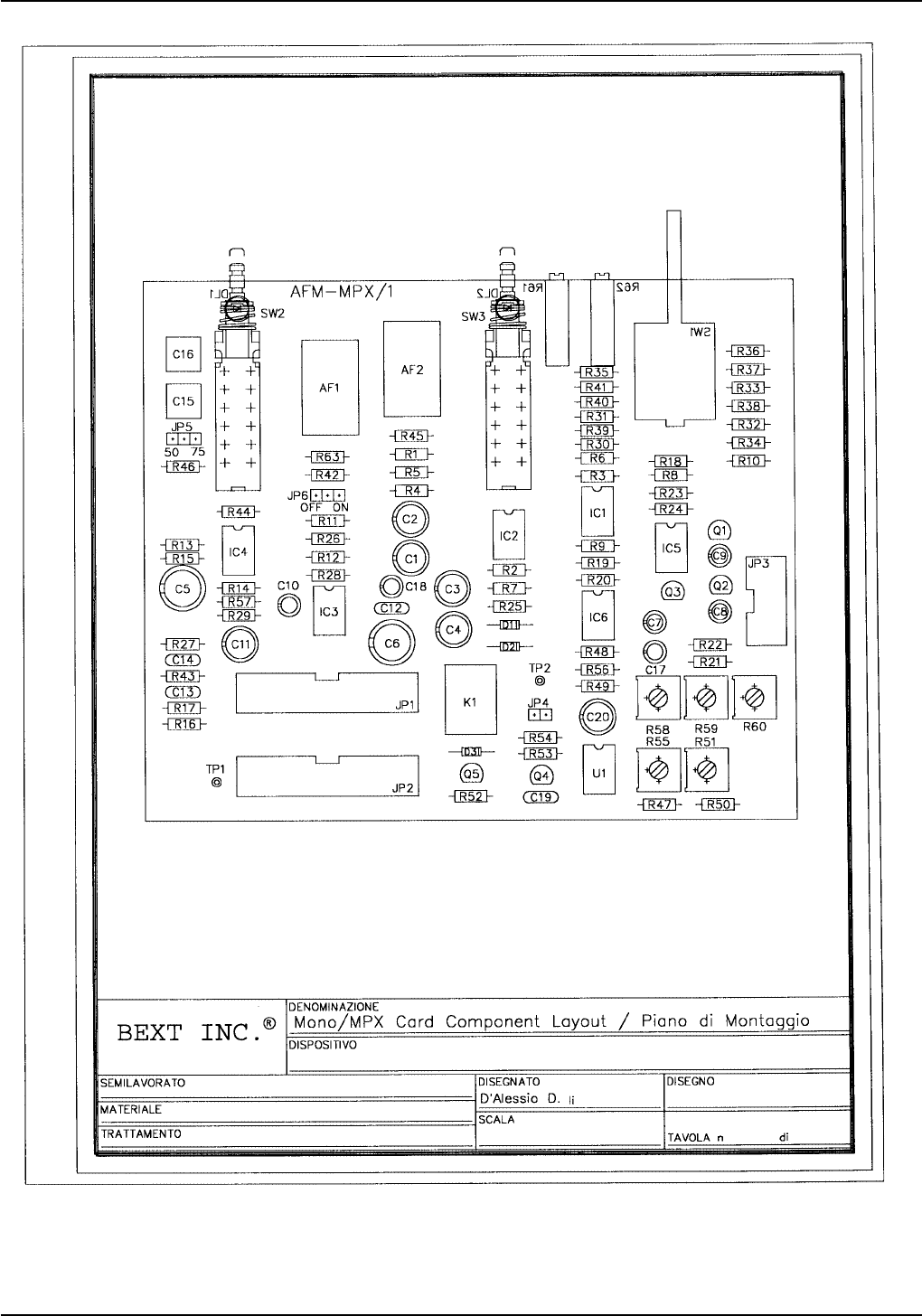
XT150 and XT150S Technical and Maintenance Manual
Pag. 108

XT150 and XT150S Technical and Maintenance Manual
Pag. 109
STEREO CODER CARDSTEREO CODER CARD
STEREO CODER CARDSTEREO CODER CARD
STEREO CODER CARD
1 Circuit Diagram Pag. 110
2 Bill of Materials Pag. 111
3 Coponent Layout Pag. 115
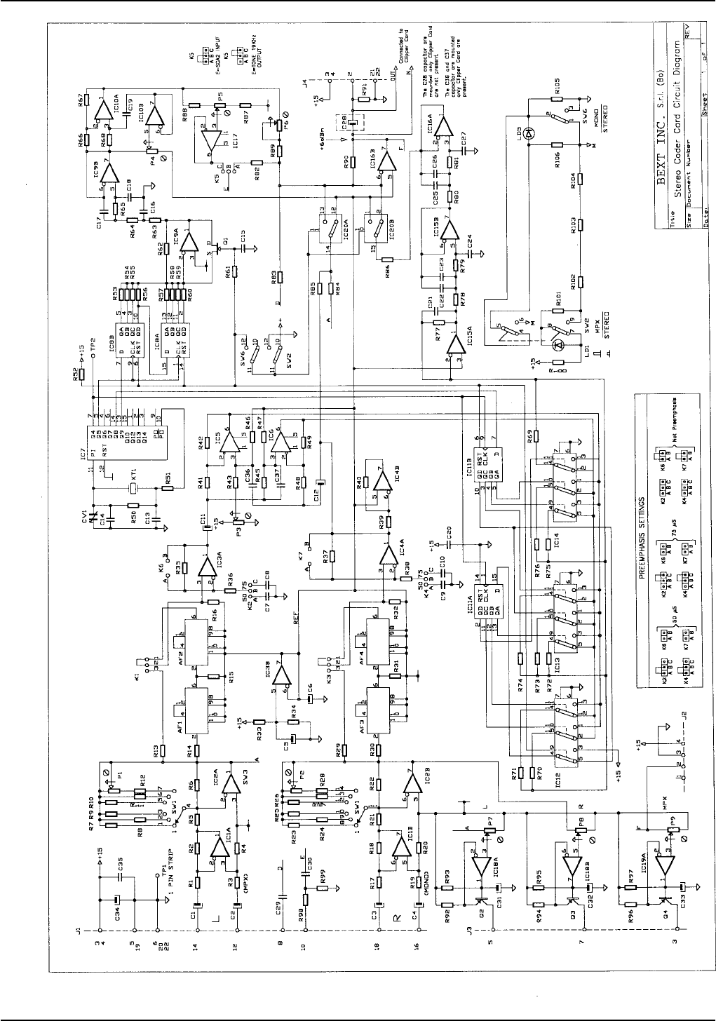
XT150 and XT150S Technical and Maintenance Manual
Pag. 110

XT150 and XT150S Technical and Maintenance Manual
Pag. 111
Stereo Coder Card Bill Of Materials Page 1
Item Quantity Reference Part Description Part Order Code
____________________________________________________________________________________________________
1 1 R98 100 RESISTOR 1/4W 5% RSC1/4JH0100
2 5 R46,R47, 200 1% RESISTOR 1/4W 1% RSC1/4FH0200
R101,R105,
R106
3 1 R51 330 RESISTOR 1/4W 5% RSC1/4JH0330
4 2 R78,R79 464 1% RESISTOR 1/4W 1% RSM1/4FH0464
5 1 R87 499 1% RESISTOR 1/4W 1% RSM1/4FH0499
6 2 R36,R38 750 1% RESISTOR 1/4W 1% RSM1/4FH0750
7 1 R100 1K RESISTOR 1/4W 5% RSC1/4JK0001
8 1 R45 1K13 2% RESISTOR 1/4W 2% RSM1/4GK1,13
9 4 R12,R28, 1K78 1% RESISTOR 1/4W 1% RSM1/4FK1,78
R80,R81
10 5 R5,R11,R21, 2K49 1% RESISTOR 1/4W 1% RSM1/4FK2,49
R27,R85
11 6 R62,R63, 3K83 1% RESISTOR 1/4W 1% RSC1/4FK3,83
R64,R65,
R66,R67
12 1 R84 4K42 1% RESISTOR 1/4W 1% RSM1/4FK4,42
13 2 R14,R30 4K64 1% RESISTOR 1/4W 1% RSM1/4FK4,64
14 10 R3,R4,R10, 5K11 1% RESISTOR 1/4W 1% RSM1/4FK5,11
R19,R20,
R26,R39,
R40,R86,
R90
15 2 R13,R29 5K90 1% RESISTOR 1/4W 1% RSM1/4FK5,90
16 2 R9,R25 7K15 1% RESISTOR 1/4W 1% RSM1/4FK7,15
17 2 R16,R32 7K50 1% RESISTOR 1/4W 1% RSM1/4FK7,50
18 1 R88 9K09 1% RESISTOR 1/4W 1% RSM1/4FK9,09
19 9 R8,R24, 10K0 1% RESISTOR 1/4W 1% RSC1/4FK10,0
R33,R34,
R41,R48,
R92,R94,
R96
20 1 R99 10K RESISTOR 1/4W 5% RSC1/4JK0010
21 1 R77 12K7 1% RESISTOR 1/4W 1% RSM1/4FK12,7

XT150 and XT150S Technical and Maintenance Manual
Pag. 112
Stereo Coder Card Bill Of Materials Page 2
Item Quantity Reference Part Description Part Order Code
____________________________________________________________________________________________________
22 6 R1,R2,R7, 14K7 1% RESISTOR 1/4W 1% RSM1/4FK14,7
R17,R18,R23
23 1 R52 15K RESISTOR 1/4W 5% RSC1/4JK0015
24 2 R42,R49 17K8 1% RESISTOR 1/4W 1% RSC1/4FK17,8
25 1 R68 20K0 1% RESISTOR 1/4W 1% RSM1/4FK20,0
26 2 R35,R37 21K5 1% RESISTOR 1/4W 1% RSM1/4FK21,5
27 2 R82,R83 24K9 1% RESISTOR 1/4W 1% RSM1/4FK24,9
28 2 R15,R31 33K RESISTOR 1/4W 5% RSC1/4JK0033
29 1 R89 40K2 1% RESISTOR 1/4W 1% RSM1/4FK40,2
30 1 R91 47K RESISTOR 1/4W 5% RSC1/4JK0047
31 4 R56,R57, 64K9 1% RESISTOR 1/4W 1% RSM1/4FK64,9
R72,R73
32 4 R55,R58, 75K0 1% RESISTOR 1/4W 1% RSM1/4FK75,0
R71,R74
33 1 R50 100K RESISTOR 1/4W 5% RSC1/4JK0100
34 4 R54,R59, 115K 1% RESISTOR 1/4W 1% RSM1/4FK0115
R70,R75
35 2 R43,R61 150K RESISTOR 1/4W 5% RSC1/4JK0150
36 4 R53,R60, 324K 1% RESISTOR 1/4W 1% RSM1/4FK0324
R69,R76
37 3 R93,R95, 470K RESISTOR 1/4W 5% RSC1/4JK0470
R97
38 2 R6,R22 1M RESISTOR 1/4W 5% RSC1/4JM0001
39 1 P5 TC1K TRIMM.REG.VERT. CERMET RVTCERVK0001
40 2 P3,P6 TC20K TRIMM.REG.VERT. CERMET RVTVERVK0020
41 3 P7,P8,P9 TC50K TRIMM.REG. VERT. CERMET RVTCERVK0050
42 2 P1,P2 M20K TRIMMER MULTIGIRI RVTMULAK0020
43 1 P4 TM5K TRIMM.MULT.REG. VERT. RVTMULVK0005
44 1 CV1 T8pF TRIMMER CAPACITOR CVC080CK600
45 1 C14 8p2 CERAMIC CAPACITOR NP0 CKM8,2BJ600C

XT150 and XT150S Technical and Maintenance Manual
Pag. 113
Stereo Coder Card Bill Of Materials Page 3
Item Quantity Reference Part Description Part Order Code
____________________________________________________________________________________________________
46 1 C23 27pF CERAMIC CAPACITOR NP0 CKM270BJ600C
47 3 C13,C21, 47PF CERAMIC CAPACITOR NP0 CKM470BJ600C
C25
48 2 C36,C37 68pF CERAMIC CAPACITOR NP0 CKM680BJ600C
49 1 C27 100pFP 1% POLIESTER CAPACITOR 1% CPE101BF63
50 2 C18,C19 150pFP 1% POLIESTER CAPACITOR 1% CPE151BF63
51 3 C16,C24, 1nFP 1% POLIESTER CAPACITOR 1% CPE102BF63
C26
52 1 C22 1n5FP 1% POLIESTER CAPACITOR 1% CPE152BF63
53 2 C7,C9 2n2P 1% POLIESTER CAPACITOR CPE222BF63
54 1 C17 2n7P 1% POLIESTER CAPACITOR 1% CPE272BF63
55 2 C8,C10 3n3P 1% POLIESTER CAPACITOR 1% CPE332BF101
56 4 C15,C20, 0.1uF CERAMIC CAPACITOR CKM104BK600P
C29,C30
57 1 C35 0.47uF POLIESTER CAPACITOR CPE474EK101
58 3 C31,C32, 2.2uF ELECTROLYTIC CAPACITOR CEA225AM630
C33
59 1 C5 10uF ELECTROLYTIC CAPACITOR CEA106AM350
60 7 C1,C2,C3, 100uF ELECTROLYTIC CAPACITOR CEA107BM350
C4,C6,
C11,C12
61 2 C28,C34 220uF ELECTROLYTIC CAPACITOR CEA227BM350
62 4 AF1,AF2, LPF19K LOW PASS FILTER 19KHZ FLP19KHZ
AF3,AF4
63 2 TP1,TP2 1 P STRIP STRIP M 1 PIN CNTSTRIPMCS
64 2 K6,K7 2 P STRIP STRIP M P 2.54 2 PIN CNTSTRIPMCS
65 5 K1,K2,K3, 3 P STRIP STRIP M P 2.54 3 PIN CNTSTRIPMCS
K4,K5
66 1 J2 4 P STRIP STRIP M P 2.54 4 PIN CNTSTRIPMCS
67 3 J1,J4,J6 26 P CONN. CONN. M 2*13 P 2.54 CNTMCSFC26P
68 1 XT1 Q9.728MHZ CRYSTAL QRZ9,728HC18

XT150 and XT150S Technical and Maintenance Manual
Pag. 114
Stereo Coder Card Bill Of Materials Page 4
Item Quantity Reference Part Description Part Order Code
____________________________________________________________________________________________________
69 1 SW1 SW2V6P COMMUTATORE 2V 6P FEME COMR2V6PCS
70 2 SW2,SW6 SWSPDT-4 COMMUTATORE 4V 2P COMR4V2PCS
71 2 LD1,LD5 LED-G5 GREEN LED DIODE LEDVE05
72 3 Q2,Q3,Q4 BC557 PNP TRANSISTOR TRNBC557
73 1 Q1 MPF4393 JFET SWITCH. N-CHANNEL TRNMPF4393
74 2 IC18,IC19 LM393 DOUBLE COMPARATOR CILLM393
75 8 IC1,IC2, LF353 DOUBLE OP. AMP. CILLF353
IC3,IC4,
IC9,IC10,
IC15,IC16
76 3 IC5,IC6, LF356 JPFET IN. OP. AMPLIFIER CILLF356
IC17
77 2 IC8,IC11 4015 SHIFT REGISTER CID4015
78 4 IC12,IC13, 4053 TRIPLE 2CH ANAL.MULTIP. CID4053
IC14,IC20
79 1 IC7 4060 CMOS BIN DIVIDER CID4060
80 3 R102,R103, WIRE COLLEGAMENTO A FILO FILO
R104
XT150 and XT150S Technical and Maintenance Manual
Pag. 115

XT150 and XT150S Technical and Maintenance Manual
Pag. 116
R.F. POWER AMPLIFIERR.F. POWER AMPLIFIER
R.F. POWER AMPLIFIERR.F. POWER AMPLIFIER
R.F. POWER AMPLIFIER
1 Circuit Diagram Pag. 117
2 Bill of Materials Pag. 118
3 Coponent Layout Pag. 119
XT150 and XT150S Technical and Maintenance Manual
Pag. 117
RF INPUT
CAV3
RG179
CAV2
RG179
CAV1
RG179
CAV4
RG179
CAV5
RG179-25
CAV6
CAVO
CN3 7CN3 8
to alarms card
RF OUTPUT
\\JACK\ SCHEDA FINALE TEX150
CSFIN150W03
1.0
TEX150
/
MANUALI\TEX150\POWER_AMP\DESIGN1.DSN
BERTI J. 23/01/01
11A4
Nome Progetto:
Autore: Codice Progetto:
Nome PC in Rete:
File/Cartella:
Data:
Revisione:
Codice:
Nome Parte:
Autorizzazione:
Pagina: Size:di
+VCC
+VCC
+VCC
CAV7
SMAF
1
2
R15 270CH
R13
270CH
R14 10CH
TR1 1K
CAV5
RG179
1
2
1
2
R2
1KCH
CAV4
RG179
1
2
C15 470pF
1
2
C19
150pFHQ
R5 1KCH
C20
100pFHQ
D2
1N4148
C25
470pFHQ
C40
470pFHQ
C29
1nF
C28
100uF C30
1nF Q4
SD1480
Q5
SD1480
C16 470pF
R1 5K6
C37
1nF
C26
0.1uF
R21 12*
C24
0.1uF
C10
680pFHQ
L13 VK
L1 VK
C6
680pFHQ
C39 1nF
C22
1nFUNELCO
L5 L59.5RVR1
C1
100uF
NC
R12
100CH
C3
1nF
C2
1nF
L9
2mH2
L11
2mH2
C18
1nF
C17 470pF
C41
470pFHQ
C38
1nF
R6 10#
C27
1nF
L12
2mH2
C21
470uF
R20
12*
C33
1nF
C32
100uF C34
1nF
L6 VK
C23
1nFUNELCO
R16 12*
L10 L43RVR0.5
Q1
TIP120
L2
L57RVR1
C13 220pF
C5
1uFP R4
1KCH
L4
L36.5RVR1
Q3
BFQ68
R17
12*
C9
470pF
C8
470pF
L7
2mH2
C11
470pFHQ
C12
470pFHQ
Q2
BLF244
L3
VK
D3
1N4148
C36
1nFUNELCO
C35
1nFUNELCO
D1
Z18V
R7
10#
CAV3
RG179
1
2
CAV2
RG179
1
2
1
2
CAV1
RG179
1
2
C31
100pFHQ
1
CAV6
CAVO
1
R3
1KCH
L8
L43RVR0.5
C14 220pF
R10 10#
R19
39#
C7
1nF
R18
39#
R11
270 R9
270 R8
100*
1
2
1
2
C4
1nF

XT150 and XT150S Technical and Maintenance Manual
Pag. 118
XT 150 (150 F.M. EXCITER) Bill Of Materials Page1
Item Q.ty Reference Part Description Part Order Code
______________________________________________________________________________________________
1 1 CAV1 RG179 CAVO SCHERMATO 25Ohm 23cm
2 2 CAV2,CAV3 RG179 CAVO SCHERMATO 25Ohm 13cm
3 2 CAV4,CAV5 RG179 CAVO SCHERMATO 25Ohm 24cm
4 1 CAV6 CAVO CAVO DIA 1.5 11.5cm
5 1 CAV7 SMAF CONN. SMA F TELAIO CNTSMAFPACRI
7 3 C1,C28,C32 100Uf ELECTROLYTIC CAPACITOR CEA107BM350
8 13 C2,C3,C4,C7,C18,C27, 1nf CERAMIC CAPACITOR CKM102BK600P
C29,C30,C33,C34,C37,
C38,C39
9 1 C5 1uFT TANATALIUM CAPACITOR
10 2 C6,C10 680pFHQ HIGH Q CAPACITOR ATC CHQ681AJ500
11 4 C8,C9,C16,C17 470pF
13 5 C11,C12,C25,C40,C41 470pFHQ HIGH Q CAPACITOR ATC CHQ471AJ500
14 2 C13,C14 220pF CERAMIC CAPACITOR NP0 CKM221BK600C
16 1 C15 470pF CERAMIC CAPACITOR CKM471BK600P
17 1 C19 150pFHQ HIGH Q CAPACITOR ATC CHQ151AJ500
18 2 C20,C31 100pFHQ HIGH Q CAPACITOR ATC CHQ101AJ500
19 1 C21 470uF ELECTROLYTIC CAPACITOR CEA477BM350
20 4 C22,C23,C35,C36 1nFUNELCO SILVER MICA CAPACITOR CSM102XK351
21 2 C26,C24 0.1uF CERAMIC CAPACITOR CKM104BK600P
24 1 D1 Z18V ZENER DIODE 18V 0.4W
25 2 D2,D3 1N4148 SILICON DIODE DIS1N4148
26 4 L1,L3,L6,L13 VK RF CHOKE IMPVK00A
27 1 L2 L57RVR1 5SP DIA7 RAME AR 1mm
28 1 L4 L36.5RVR1 3SP DIA6.5 RAME AR 1mm
29 1 L5 L59.5RVR1 5SP DIA9.5 RAME AR 1mm
30 4 L7,L9,L11,L12 2mH2 IMPEDENZA
31 2 L10,L8 L43RVR0.5 4 SP DIA3 RAME SM 0.5mm
32 1 NC N.C. NON CONNESSO
33 1 Q1 TIP120 NPN DARLINGTON TRNTIP120
34 1 Q2 BLF244 TRANSISTOR BLF244 TRNBLF244
35 1 Q3 BFQ68 NPN RF TRANSISTOR TRNBFQ68
36 2 Q4,Q5 SD1480 RF POWER TRANSISTOR TRNSD1480
37 1 R1 5K6 RESISTOR 1/4W 5% RSC1/4JK0001
38 4 R2,R3,R4,R5 1KCH CHIP RESISTOR RCH085J0001K
39 3 R6,R7,R10 10# RESISTOR 2W RSC002JH0010
40 1 R8 100* RESISTOR 1/2W 5% RSC1/2JH0100
41 2 R11,R9 270 RESISTOR 1/4W 5% RSC1/4JH0270
42 1 R12 100CH CHIP RESISTOR
43 2 R15,R13 270CH CHIP RESISTOR RCH085J0270H
44 1 R14 10CH CHIP RESISTOR RCH1/4JH0010
45 4 R16,R17,R20,R21 12* RESISTOR 1/2W 5% RSC1/2JH012
46 2 R19,R18 39# RESISTOR 2W RSC002JH0039
47 1 TR1 1K
XT150 and XT150S Technical and Maintenance Manual
Pag. 119

XT150 and XT150S Technical and Maintenance Manual
Pag. 120
LOW PASS FILTERLOW PASS FILTER
LOW PASS FILTERLOW PASS FILTER
LOW PASS FILTER
1 Circuit Diagram Pag. 121
2 Bill of Materials Pag. 122
3 Coponent Layout Pag. 123
XT150 and XT150S Technical and Maintenance Manual
Pag. 121

XT150 and XT150S Technical and Maintenance Manual
Pag. 122
Low Pass Filter Bill Of Materials Page 1
Item Quantity Reference Part Description Part Order Code
____________________________________________________________________________________________________
1 2 C19,C33 4p7FHQ HIGHT Q CAPACITOR CHQ4,7AJ500
2 1 C18 10pFHQ HIGHT Q CAPACITOR CHQ100AJ500
3 8 C16,C17, 27pFUNELCO SILVER MICA CAPACITOR CSM270XK351
C20,C21,
C22,C23,
C24,C25
4 1 C1 1nFPAS CERAMIC THROUGH CAPAC. CDP102XK500
5 2 L5,L6 L28RVR1.5 2SP D8 RAME ARG. 1.5mm BFS15000208
6 3 L7,L8,L9 L410RVR2 4SP D10 RAME ARG. 2.0mm BFS20000410
7 1 J1 SMAF CONN. SMA F TELAIO CNTSMAF
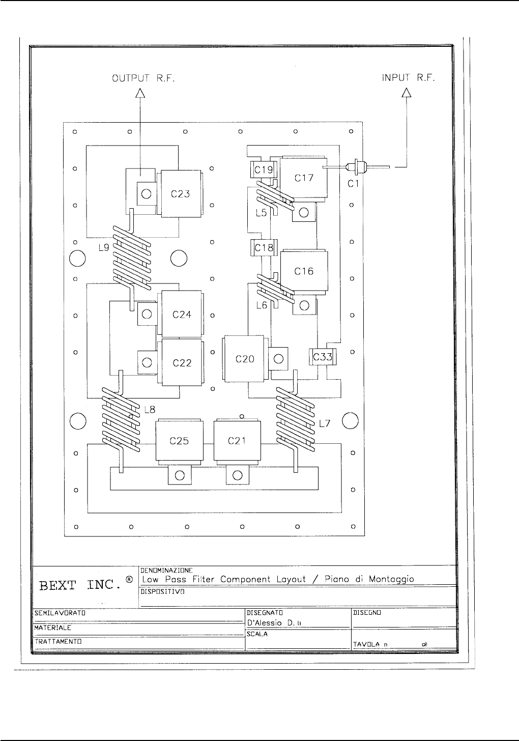
XT150 and XT150S Technical and Maintenance Manual
Pag. 123

XT150 and XT150S Technical and Maintenance Manual
Pag. 124
DIRECTIONAL COUPLERDIRECTIONAL COUPLER
DIRECTIONAL COUPLERDIRECTIONAL COUPLER
DIRECTIONAL COUPLER
1 Circuit Diagram Pag. 125
2 Bill of Materials Pag. 126
3 Coponent Layout Pag. 127
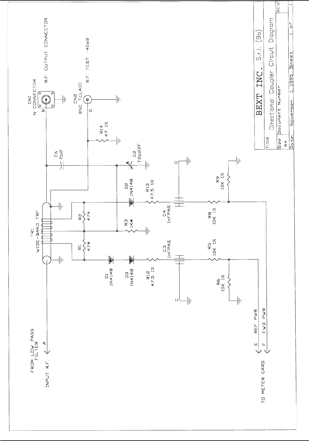
XT150 and XT150S Technical and Maintenance Manual
Pag. 125

XT150 and XT150S Technical and Maintenance Manual
Pag. 126
Directional Coupler Bill Of Materials Page 1
Item Quantity Reference Part Description Part Order Code
____________________________________________________________________________________________________
1 1 R14 47 1% RESISTOR 1/4W 1% RSM1/4FH0047
2 2 R1,R2 47# RESISTOR 2W RSC002JH0047
3 2 R12,R13 47.5 1% RESISTOR 1/4W 1% RSM1/4FH47.5
4 1 R3 1K* RESISTOR 1/2W 5% RSC1/2JK0001
5 4 R5,R6,R8,R9 10K 1% RESISTOR 1/4W 1% RSM1/4FK0010
6 1 C6 2p2 CERAMIC CAPACITOR NP0 CKM2,2BJ600C
7 1 C2 T2p22F TRIMMER CAPACITOR CVC2,22CK600
8 2 C3,C4 1nFPAS CERAMIC THROUGH CAPAC. CDP102XK500
9 1 CN2 BNC TELAIO CONN. BNC A TELAIO CNTBNCFPV
10 1 CN1 N CONNECTOR CONN. N A TELAIO CNTNFPFL
11 3 D1,D2,D3 1N4148 SILICON DIODE DIS1N4148
12 1 TR1 WIDE-BAND WIDE-BAND TRANSFORMER TRFWIDEBAND
TRF
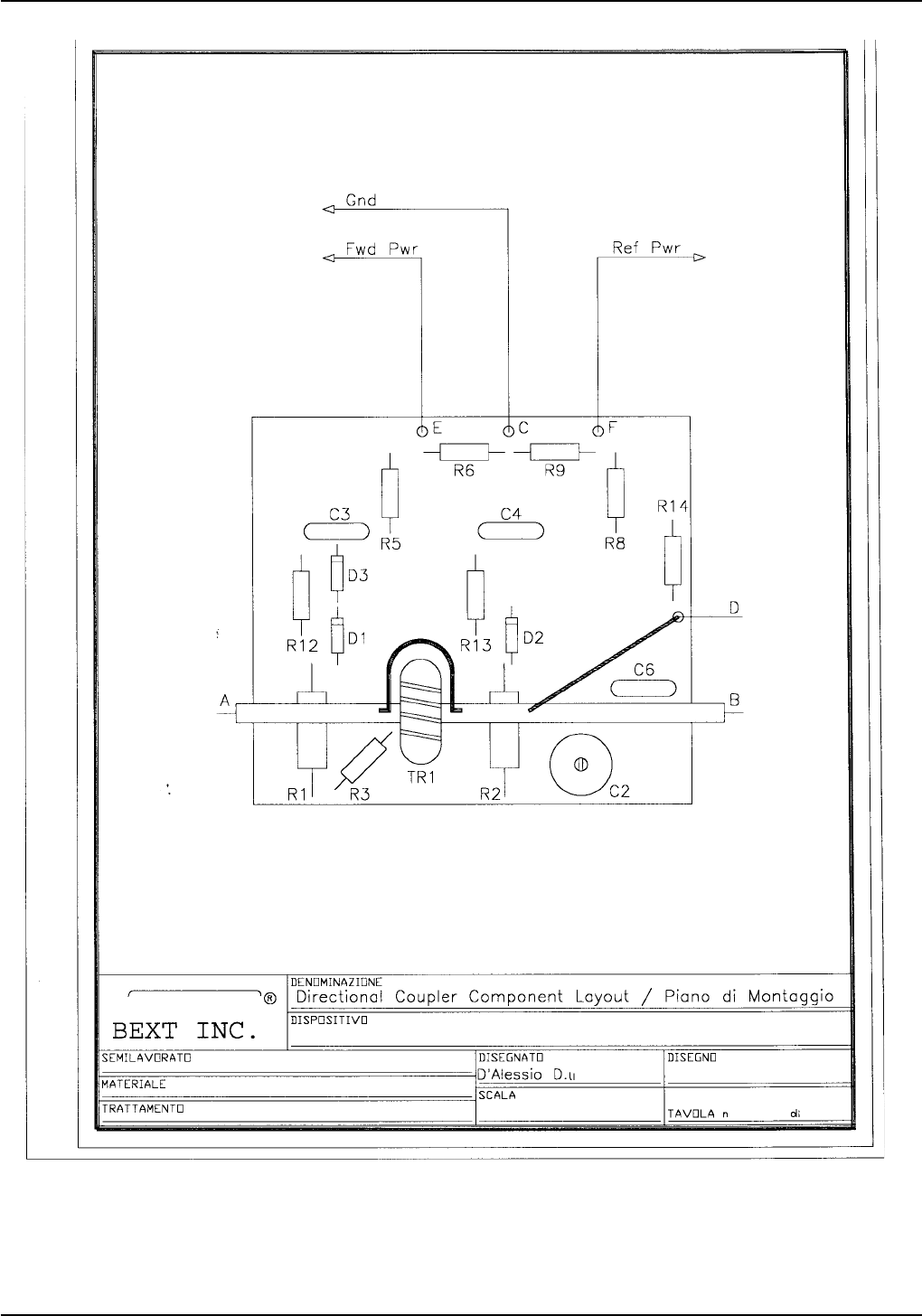
XT150 and XT150S Technical and Maintenance Manual
Pag. 127

XT150 and XT150S Technical and Maintenance Manual
Pag. 128
CLIPPER CARDCLIPPER CARD
CLIPPER CARDCLIPPER CARD
CLIPPER CARD
1 Circuit Diagram Pag. 129
2 Bill of Materials Pag. 130
3 Coponent Layout Pag. 131
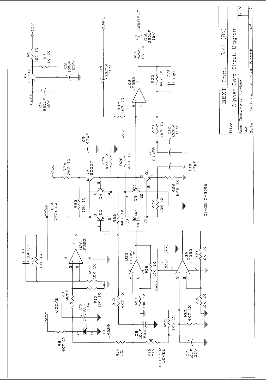
XT150 and XT150S Technical and Maintenance Manual
Pag. 129

XT150 and XT150S Technical and Maintenance Manual
Pag. 130
Clipper Card Bill Of Materials Page 2
Item Quantity Reference Part Description Part Order Code
____________________________________________________________________________________________________
1 1 R6 100 1% RESISTOR 1/4W 1% RSM1/4FH0100
2 1 R7 1K 1% RESISTOR 1/4W 1% RSM1/4FK0001
3 1 R15 1K5 1% RESISTOR 1/4W 1% RSC1/4FK01,5
4 2 R24,R28 2K2 1% RESISTOR 1/4W 1% RSC1/4FK02,2
5 7 R8,R13,R21, 4K7 1% RESISTOR 1/4W 1% RSM1/4FK04,7
R22,R29,
R30,R32
6 10 R10,R11, 10K 1% RESISTOR 1/4W 1% RSM1/4FK0010
R12,R17,
R18,R19,
R20,R23,
R27,R31
7 2 R25,R26 47K 1% RESISTOR 1/4W 1% RSM1/4FK0047
8 1 R16 M1K TRIMMER MULTIGIRI RVTMULAK0001
9 1 R9 M20K TRIMMER MULTIGIRI RVTMULAK0020
10 1 C13 10pF CERAMIC CAPACITOR NP0 CKM100BJ600C
11 2 C9,C10 47pF CERAMIC CAPACITOR NP0 CKM470BJ600C
12 2 C1,C14 0.1uF CERAMIC CAPACITOR CKM104BK600P
13 1 C11 0.1uFP POLIESTER CAPACITOR CPE104DK101
14 1 C6 0.47uF POLIESTER CAPACITOR CPE474EK101
15 3 C5,C7,C8 10uF ELECTROLYTIC CAPACITOR CEA106AM350
16 1 C3 100uF ELECTROLYTIC CAPACITOR CEA107BM350
17 4 C4,C12, 220uF ELECTROLYTIC CAPACITOR CEA227BM350
C15,C16
18 5 Q1,Q2,Q3, CA3096 NPN/PNP TRANSIST. ARRAY CILCA3096
Q4,Q5
19 1 D1 LM329 VOLT.PRECISION REFER. CILLM329
20 1 Q6 BC237 NPN TRANSISTOR TRNBC237
21 1 Q7 BC557 PNP TRANSISTOR TRNBC557
22 2 U2,U3 LF353 DOUBLE OP. AMP. CILLF353
23 1 R14 N.C. NOT CONNECTED
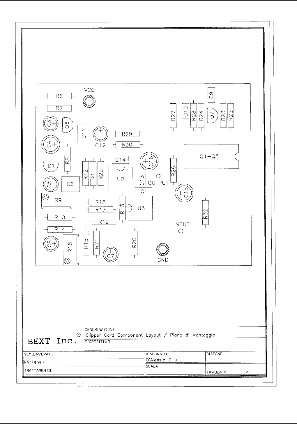
XT150 and XT150S Technical and Maintenance Manual
Pag. 131

XT150 and XT150S Technical and Maintenance Manual
Pag. 132
150PS2 CARD150PS2 CARD
150PS2 CARD150PS2 CARD
150PS2 CARD
1 Circuit Diagram Pag. 133
2 Bill of Materials Pag. 134
3 Coponent Layout Pag. 135
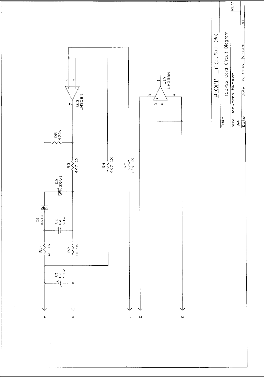
XT150 and XT150S Technical and Maintenance Manual
Pag. 133

XT150 and XT150S Technical and Maintenance Manual
Pag. 134
150PS2 Card Bill Of Materials Page 1
Item Quantity Reference Part Description Part Order Code
____________________________________________________________________________________________________
1 1 R1 100 1% RESISTOR 1/4W 1% RSM1/4FH0100
2 1 R2 1K 1% RESISTOR 1/4W 1% RSM1/4FK0001
3 2 R3,R4 4K7 1% RESISTOR 1/4W 1% RSM1/4FK04,7
4 1 R5 12K 1% RESISTOR 1/4W 1% RSM1/4FK0012
5 1 R5 470K RESISTOR 1/4W 5% RSC1/4JK0470
6 2 C1,C2 1µF ELECTROLYTIC CAPACITOR CEA105AM630
7 1 D1 BAT42 HOT CARRIER DIODE DHCBAT42
8 1 D2 Z9V1 ZENER DIODE 9.1V 0.4W DIZ9V10W4
9 1 U1 LM358N DOUBLE OP. AMP. CILLM358N
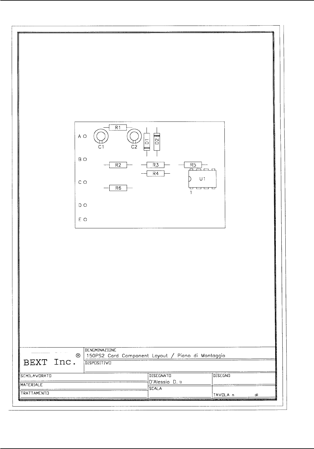
XT150 and XT150S Technical and Maintenance Manual
Pag. 135

XT150 and XT150S Technical and Maintenance Manual
Pag. 136
STEREO CODER CARD (Mod. SDC30A002)STEREO CODER CARD (Mod. SDC30A002)
STEREO CODER CARD (Mod. SDC30A002)STEREO CODER CARD (Mod. SDC30A002)
STEREO CODER CARD (Mod. SDC30A002)
1 Circuit Diagram Pag. 137
2 Bill of Materials Pag. 140
3 Coponent Layout Pag. 150
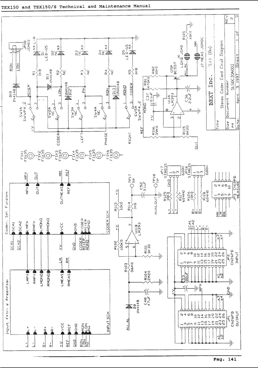
XT150 and XT150S Technical and Maintenance Manual
Pag. 137
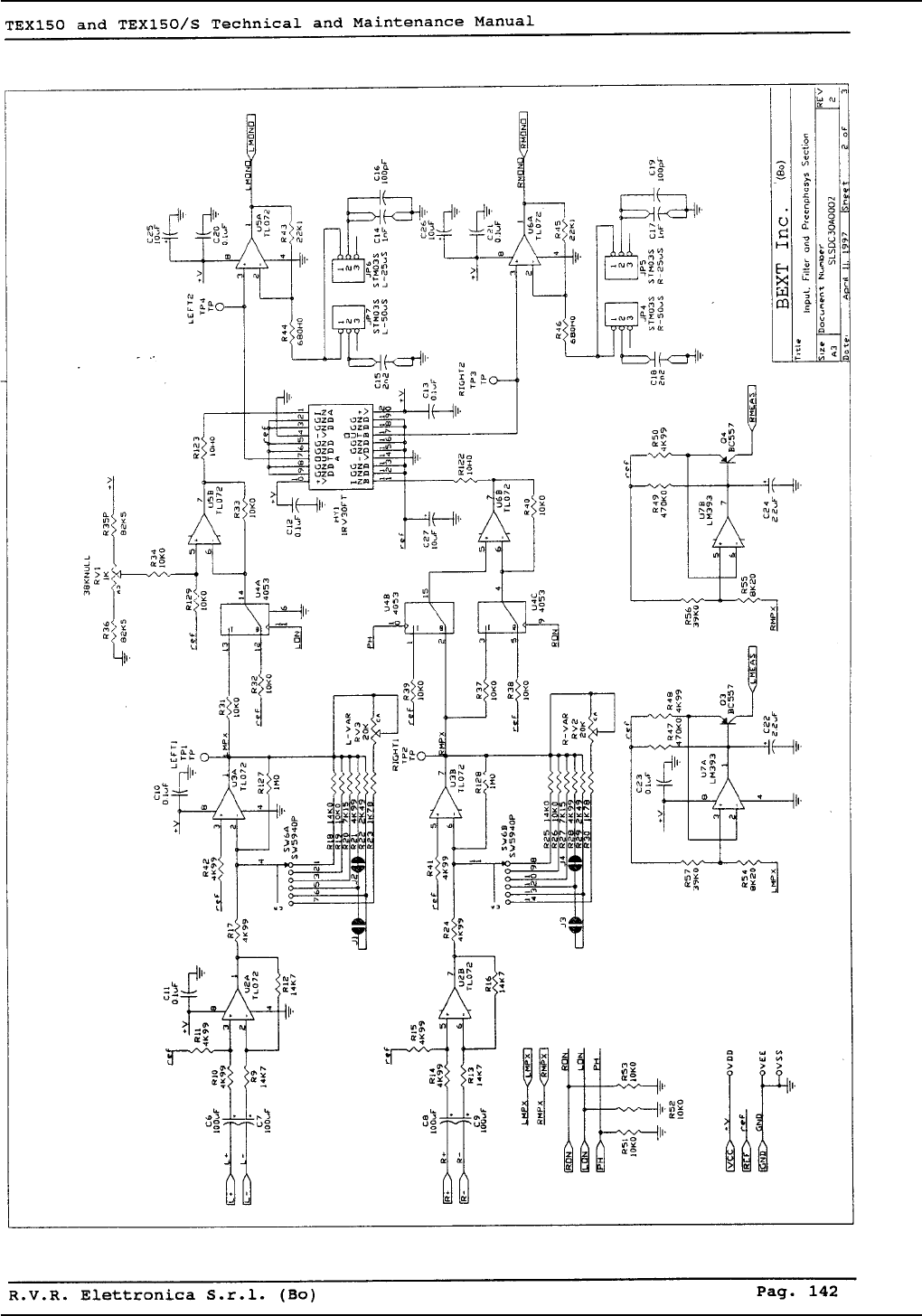
XT150 and XT150S Technical and Maintenance Manual
Pag. 138
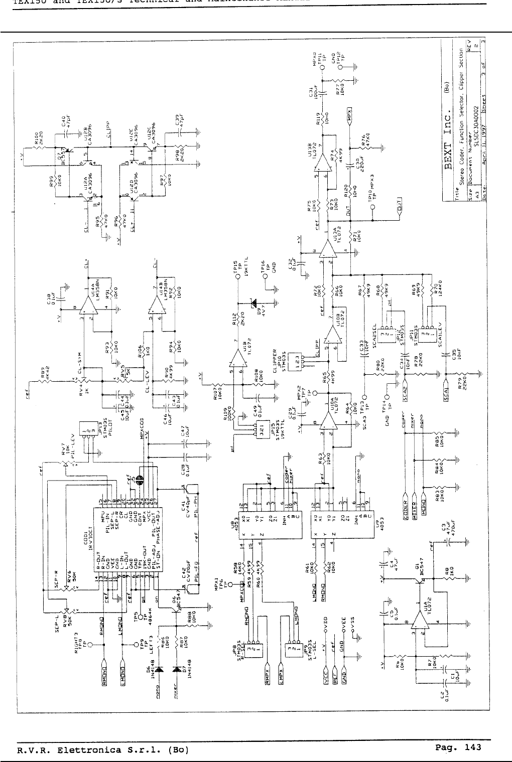
XT150 and XT150S Technical and Maintenance Manual
Pag. 139

XT150 and XT150S Technical and Maintenance Manual
Pag. 140
Stereo Coder Bill Of Materials Page 1
Item Reference Part Description Part Order Code
____________________________________________________________________________________________________
1 CS1 CS PC Board CSSDC30A0002
2 R1 1K8 Res. 1/4 W 1% RSM1/4FK01,8
3 R5 1K8 Res. 1/4 W 1% RSM1/4FK01,8
4 R117 604H0 Res. 1/4 W 1% RSM1/4FH0604
5 R118 604H0 Res. 1/4 W 1% RSM1/4FH0604
6 D1 LED-G5 Led Green dia. 5mm LEDVE05
7 D5 LED-G5 Led Green dia. 5mm LEDVE05
8 D8 1N4148 Silicon Diode DIS1N4148
9 C48 47uF Electrolitic Cap.16V p. 2.5mm CEA476AM160
10 R104 2M20 Res. 1/4 W 1% RSM1/4FM02,2
11 R103 56K0 Res. 1/4 W 1% RSM1/4FK0056
12 R114 1K0 Res. 1/4 W 1% RSM1/4FK0001
13 R125 10K0 Res. 1/4 W 1% RSM1/4FK0010
14 R126 10K0 Res. 1/4 W 1% RSM1/4FK0010
15 JP17 STM03S Strip M 2.54 3 pin. CNTSTM03S
16 JP16 STM03S Strip M 2.54 3 pin. CNTSTM03S
17 JP2 CN26PD Conn. M cs 2x2.54mm 26 pin. CNTMCSFC26P
18 JP3 CN10PD Conn. M cs 2x2.54mm 10 pin. CNTMCSFC10P
19 JP1 CN26PD Conn. M cs 2x2.54mm 26 pin. CNTMCSFC26P
20 C52 0.1uF Ceramic Capacitor p. 5mm P100 CKM104BK600P
21 SW1 SWWP4_2 Rotary Switch SWWP4_2
22 SW5 SWWP4_2 Rotary Switch SWWP4_2
23 C53 100uF Electrolitic Cap 25V p. 2.5mm CEA107AM250
24 SW2 NC Not connected
25 R2 NC Not connected
26 D2 NC Not connected
27 D3 NC Not connected

XT150 and XT150S Technical and Maintenance Manual
Pag. 141
Stereo Coder Bill Of Materials Page 2
Item Reference Part Description Part Order Code
____________________________________________________________________________________________________
28 R3 NC Not connected
29 SW3 NC Not connected
30 SW4 NC Not connected
31 R4 NC Not connected
32 D4 NC Not connected
33 D10 1N4148 Silicon Diode DIS1N4148
34 D11 1N4148 Silicon Diode DIS1N4148
35 D12 1N4148 Silicon Diode DIS1N4148
36 D13 1N4148 Silicon Diode DIS1N4148
37 C37 0.1uF Ceramic Cap. p. 5mm P100 CKM104BK600P
38 R81 470K0 Res. 1/4 W 1% RSM1/4FK0470
39 R82 10K0 Res. 1/4 W 1% RSM1/4FK0010
40 R116 39K0 Res. 1/4 W 1% RSM1/4FK0039
41 R115 8K20 Res. 1/4 W 1% RSM1/4FK08,2
42 R105 10K0 Res. 1/4 W 1% RSM1/4FK0010
43 U11 LM393 IC linear CILLM393
44 ZOC11 ZOC8 Socket 8 pin ZIN08
45 R102 100K0 Res. 1/4 W 1% RSM1/4FK0100
46 R101 3K30 Res. 1/4 W 1% RSM1/4FK03,3
47 C36 2.2uF Electrolitic Cap.16V p. 2.5mm CEA225AM160
48 R113 10K0 Res. 1/4 W 1% RSM1/4FK0010
49 Q5P BC557 Tr. in TO 92 TRNBC557
50 U2 TL072 IC linear CILTL072
51 ZOC2 ZOC8 Socket 8 pin ZIN08
52 U5 TL072 IC linear CILTL072
53 ZOC5 ZOC8 Socket 8 pin ZIN08
54 U6 TL072 IC linear CILTL072
55 ZOC6 ZOC8 Socket 8 pin ZIN08

XT150 and XT150S Technical and Maintenance Manual
Pag. 142
Stereo Coder Bill Of Materials Page 3
Item Reference Part Description Part Order Code
____________________________________________________________________________________________________
56 U3 TL072 IC linear CILTL072
57 ZOC3 ZOC8 Socket 8 pin ZIN08
58 U7 LM393 IC lineare CILLM393
59 ZOC7 ZOC8 Socket 8 pin ZIN08
60 C6 100uF Electrolitic Cap.25V p. 2.5mm CEA107AM250
61 C7 100uF Electrolitic Cap.25V p. 2.5mm CEA107AM250
62 R9 14K7 Res. 1/4 W 1% RSM1/4FK14,7
63 R10 4K99 Res. 1/4 W 1% RSM1/4FK4,99
64 R11 4K99 Res. 1/4 W 1% RSM1/4FK4,99
65 R12 14K7 Res. 1/4 W 1% RSM1/4FK14,7
66 C11 0.1uF Ceramic Cap. p. 5mm P100 CKM104BK600P
67 C10 0.1uF Ceramic Cap. p. 5mm P100 CKM104BK600P
68 R31 10K0 Res. 1/4 W 1% RSM1/4FK0010
69 R33 10K0 Res. 1/4 W 1% RSM1/4FK0010
70 C27 10uF Electrolitic Cap.35V p. 2.5mm CEA106AM350
71 C13 0.1uF Ceramic Cap. p. 5mm P100 CKM104BK600P
72 R44 680H0 Res. 1/4 W 1% RSM1/4FH0680
73 R43 22K1 Res. 1/4 W 1% RSM1/4FK22,1
74 C14 1nF Capacitor 1% p. 7mm CPS102CF630
75 C16 100pF Ceramic Cap. p. 5mm NP0 CKM101BK600C
76 C20 0.1uF Ceramic Cap. p. 5mm P100 CKM104BK600P
77 C25 10uF Electrolitic Cap.35V p. 2.5mm CEA106AM350
78 C26 10uF Electrolitic Cap.35V p. 2.5mm CEA106AM350
79 C21 0.1uF Ceramic Cap. p. 5mm P100 CKM104BK600P
80 R45 22K1 Res. 1/4 W 1% RSM1/4FK22,1
81 R46 680H0 Res. 1/4 W 1% RSM1/4FH0680
82 C18 2.2nF Capacitor 1% p. 7mm CPS222CF630
83 C15 2.2nF Capacitor 1% p. 7mm CPS222CF630

XT150 and XT150S Technical and Maintenance Manual
Pag. 143
Stereo Coder Bill Of Materials Page 4
Item Reference Part Description Part Order Code
____________________________________________________________________________________________________
84 C17 1nF Capacitor 1% p. 7mm CPS102CF630
85 C19 100pF Ceramic Cap. p. 5mm NP0 CKM101BK600C
86 R40 10K0 Res. 1/4 W 1% RSM1/4FK0010
87 R37 10K0 Res. 1/4 W 1% RSM1/4FK0010
88 R39 10K0 Res. 1/4 W 1% RSM1/4FK0010
89 R14 4K99 Res. 1/4 W 1% RSM1/4FK4,99
90 R15 4K99 Res. 1/4 W 1% RSM1/4FK4,99
91 R13 14K7 Res. 1/4 W 1% RSM1/4FK14,7
92 R16 14K7 Res. 1/4 W 1% RSM1/4FK14,7
93 C9 100uF Electrolitic Cap.25V p. 2.5mm CEA107AM250
94 C8 100uF Electrolitic Cap.25V p. 2.5mm CEA107AM250
95 R51 10K0 Res. 1/4 W 1% RSM1/4FK0010
96 R52 10K0 Res. 1/4 W 1% RSM1/4FK0010
97 R53 10K0 Res. 1/4 W 1% RSM1/4FK0010
98 R57 39K0 Res. 1/4 W 1% RSM1/4FK0039
99 R54 8K20 Res. 1/4 W 1% RSM1/4FK08,2
100 C22 2.2uF Electrolitic Cap.16V p. 2.5mm CEA225AM160
101 R47 470K0 Res. 1/4 W 1% RSM1/4FK0470
102 C23 0.1uF Ceramic Cap. p. 5mm P100 CKM104BK600P
103 Q3 BC557 Tr. in TO 92 TRNBC557
104 R55 8K20 Res. 1/4 W 1% RSM1/4FK08,2
105 R56 39K0 Res. 1/4 W 1% RSM1/4FK0039
106 R49 470K0 Res. 1/4 W 1% RSM1/4FK0470
107 Q4 BC557 Tr. in TO 92 TRNBC557
108 C24 2.2uF Electrolitic Cap.16V p. 2.5mm CEA225AM160
109 R19 10K0 Res. 1/4 W 1% RSM1/4FK0010
110 R20 7K15 Res. 1/4 W 1% RSM1/4FK7,15
111 R22 2K49 Res. 1/4 W 1% RSM1/4FK2,49

XT150 and XT150S Technical and Maintenance Manual
Pag. 144
Stereo Coder Bill Of Materials Page 5
Item Reference Part Description Part Order Code
____________________________________________________________________________________________________
112 R23 1K78 Res. 1/4 W 1% RSM1/4FK1,78
113 R26 10K0 Res. 1/4 W 1% RSM1/4FK0010
114 R27 7K15 Res. 1/4 W 1% RSM1/4FK7,15
115 R29 2K49 Res. 1/4 W 1% RSM1/4FK2,49
116 R30 1K78 Res. 1/4 W 1% RSM1/4FK1,78
117 C12 0.1uF Ceramic Cap. p. 5mm P100 CKM104BK600P
118 RV1 1K Multi Turn Pot. 3296W rg V RVTMTJVK0001
119 JP4 STM03S Strip M 2.54 3 pin. CNTSTM03S
120 JP5 STM03S Strip M 2.54 3 pin. CNTSTM03S
121 JP7 STM03S Strip M 2.54 3 pin. CNTSTM03S
122 R127 1M0 Res. 1/4 W 1% RSM1/4FM0001
123 R128 1M0 Res. 1/4 W 1% RSM1/4FM0001
124 SW6 SW5940P Rotary Switch SW5940P
125 U4 4053 IC digital CID4053
126 ZOC4 ZOC16 Socket 16 pin ZIN16
127 R38 10K0 Res. 1/4 W 1% RSM1/4FK0010
128 R32 10K0 Res. 1/4 W 1% RSM1/4FK0010
129 R17 4K99 Res. 1/4 W 1% RSM1/4FK4,99
130 R24 4K99 Res. 1/4 W 1% RSM1/4FK4,99
131 R41 4K99 Res. 1/4 W 1% RSM1/4FK4,99
132 R42 4K99 Res. 1/4 W 1% RSM1/4FK4,99
133 R21 4K99 Res. 1/4 W 1% RSM1/4FK4,99
134 R18 14K0 Res. 1/4 W 1% RSM1/4FK0014
135 R25 14K0 Res. 1/4 W 1% RSM1/4FK0014
136 R28 4K99 Res. 1/4 W 1% RSM1/4FK4,99
137 R48 4K99 Res. 1/4 W 1% RSM1/4FK4,99
138 R50 4K99 Res. 1/4 W 1% RSM1/4FK4,99
139 R123 10H0 Res. 1/4 W 1% RSM1/4FH0010

XT150 and XT150S Technical and Maintenance Manual
Pag. 145
Stereo Coder Bill Of Materials Page 6
Item Reference Part Description Part Order Code
____________________________________________________________________________________________________
140 R122 10H0 Res. 1/4 W 1% RSM1/4FH0010
141 JP6 STM03S Strip M 2.54 3 pin. CNTSTM03S
142 RV2 20K Multi Turn Pot. rg H RVTMTDHK0020
143 RV3 20K Multi Turn Pot. rg H RVTMTDHK0020
144 R34 10K0 Res. 1/4 W 1% RSM1/4FK0010
145 R129 10K0 Res. 1/4 W 1% RSM1/4FK0010
146 R36 82K5 Res. 1/4 W 1% RSM1/4FK82,5
147 R35P 82K5 Res. 1/4 W 1% RSM1/4FK82,5
148 HY1 IRV30FT Code Filter IRV30FT MIBIRV30FT
149 U8 4053 IC digital CID4053
150 ZOC8 ZOC16 Socket 16 pin ZIN16
151 U9 4053 IC digital CID4053
152 ZOC9 ZOC16 Socket 16 pin ZIN16
153 C30 220uF Electrolitic Cap.16V p. 2.5mm CEA227AM160
154 U12 CA3096 IC linear CILCA3096
155 ZOC12 ZOC16 Socket 16 pin ZIN16
156 U10 TL072 IC linear CILTL072
157 ZOC10 ZOC8 Socket 8 pin ZIN08
158 U13 TL072 IC linear CILTL072
159 ZOC13 ZOC8 Socket 8 pin ZIN08
160 U14 LM358N IC linear CILLM358N
161 ZOC14 ZOC8 Socket 8 pin ZIN08
162 C47 10uF Electrolitic Cap.35V p. 2.5mm CEA106AM350
163 C28 0.1uF Ceramic Cap. p. 5mm P100 CKM104BK600P
164 Q6 BC547 Tr. in TO 92 TRNBC547
165 R88 10K0 Res. 1/4 W 1% RSM1/4FK0010
166 R87 10K0 Res. 1/4 W 1% RSM1/4FK0010
167 R86 10K0 Res. 1/4 W 1% RSM1/4FK0010

XT150 and XT150S Technical and Maintenance Manual
Pag. 146
Stereo Coder Bill Of Materials Page 7
Item Reference Part Description Part Order Code
____________________________________________________________________________________________________
168 D6 1N4148 Silicon Diode DIS1N4148
169 D7 1N4148 Silicon Diode DIS1N4148
170 R59 4K99 Res. 1/4 W 1% RSM1/4FK4,99
171 R60 4K99 Res. 1/4 W 1% RSM1/4FK4,99
172 R61 10K0 Res. 1/4 W 1% RSM1/4FK0010
173 R62 10K0 Res. 1/4 W 1% RSM1/4FK0010
174 R63 10K0 Res. 1/4 W 1% RSM1/4FK0010
175 R64 10K0 Res. 1/4 W 1% RSM1/4FK0010
176 C29 0.1uF Ceramic Cap. p. 5mm P100 CKM104BK600P
177 R65 4K99 Res. 1/4 W 1% RSM1/4FK4,99
178 R72 10K0 Res. 1/4 W 1% RSM1/4FK0010
179 R66 10K0 Res. 1/4 W 1% RSM1/4FK0010
180 C32 0.1uF Ceramic Cap. p. 5mm P100 CKM104BK600P
181 R71 10K0 Res. 1/4 W 1% RSM1/4FK0010
182 R73 10K0 Res. 1/4 W 1% RSM1/4FK0010
183 R75 10K0 Res. 1/4 W 1% RSM1/4FK0010
184 R74 4K99 Res. 1/4 W 1% RSM1/4FK4,99
185 R119 10H0 Res. 1/4 W 1% RSM1/4FH0010
186 C31 100uF Electrolitic Cap.25V p. 2.5mm CEA107AM250
187 R77 10K0 Res. 1/4 W 1% RSM1/4FK0010
188 R120 10H0 Res. 1/4 W 1% RSM1/4FH0010
189 R79 22K0 Res. 1/4 W 1% RSM1/4FK0022
190 R78 22K0 Res. 1/4 W 1% RSM1/4FK0022
191 R80 22K0 Res. 1/4 W 1% RSM1/4FK0022
192 R67 49K9 Res. 1/4 W 1% RSM1/4FK49,9
193 R68 49K9 Res. 1/4 W 1% RSM1/4FK49,9
194 R69 49K9 Res. 1/4 W 1% RSM1/4FK49,9
195 R70 124K0 Res. 1/4 W 1% RSM1/4FK0124

XT150 and XT150S Technical and Maintenance Manual
Pag. 147
Stereo Coder Bill Of Materials Page 8
Item Reference Part Description Part Order Code
____________________________________________________________________________________________________
196 R83 10K0 Res. 1/4 W 1% RSM1/4FK0010
197 R84 10K0 Res. 1/4 W 1% RSM1/4FK0010
198 R85 10K0 Res. 1/4 W 1% RSM1/4FK0010
199 C39 47pF Ceramic Cap. p. 5mm NP0 CKM470BK600C
200 R98 2K20 Res. 1/4 W 1% RSM1/4FK02,2
201 R97 10K0 Res. 1/4 W 1% RSM1/4FK0010
202 R96 47K0 Res. 1/4 W 1% RSM1/4FK0047
203 R95 47K0 Res. 1/4 W 1% RSM1/4FK0047
204 Q7 BC557 Tr. in TO 92 TRNBC557
205 C40 47pF Ceramic Cap. p. 5mm NP0 CKM470BK600C
206 R100 2K20 Res. 1/4 W 1% RSM1/4FK02,2
207 C38 0.1uF Ceramic Cap. p. 5mm P100 CKM104BK600P
208 R91 10K0 Res. 1/4 W 1% RSM1/4FK0010
209 R93 10K0 Res. 1/4 W 1% RSM1/4FK0010
210 R92 10K0 Res. 1/4 W 1% RSM1/4FK0010
211 R94 10K0 Res. 1/4 W 1% RSM1/4FK0010
212 R90 4K99 Res. 1/4 W 1% RSM1/4FK4,99
213 C43 0.1uF Ceramic Cap. p. 5mm P100 CKM104BK600P
214 C46 10uF Electrolitic Cap.35V p. 2.5mm CEA106AM350
215 C45 10uF Elecrtolitic Cap.35V p. 2.5mm CEA106AM350
216 C44 0.1uF Ceramic Cap. p. 5mm P100 CKM104BK600P
217 R106 1K0 Res. 1/4 W 1% RSM1/4FK0001
218 R89 4K42 Res. 1/4 W 1% RSM1/4FK4,42
219 R109 100K0 Res. 1/4 W 1% RSM1/4FK0100
220 C49 0.1uF Ceramic Cap. p. 5mm P100 CKM104BK600P
221 R108 10K0 Res. 1/4 W 1% RSM1/4FK0010
222 D9 4V7 Zener Diode 0.4 W DIZ4V70W4
223 R76 47K0 Res. 1/4 W 1% RSM1/4FK0047

XT150 and XT150S Technical and Maintenance Manual
Pag. 148
Stereo Coder Bill Of Materials Page 9
Item Reference Part Description Part Order Code
____________________________________________________________________________________________________
224 JP13 STM03S Strip M 2.54 3 pin. CNTSTM03S
225 JP15 STM03S Strip M 2.54 3 pin. CNTSTM03S
226 JP10 STM03S Strip M 2.54 3 pin. CNTSTM03S
227 JP12 STM03S Strip M 2.54 3 pin. CNTSTM03S
228 JP11 STM03S Strip M 2.54 3 pin. CNTSTM03S
229 R99 10K0 Res. 1/4 W 1% RSM1/4FK0010
230 R107 10K0 Res. 1/4 W 1% RSM1/4FK0010
231 R112 2K20 Res. 1/4 W 1% RSM1/4FK02,2
232 R6 10K0 Res. 1/4 W 1% RSM1/4FK0010
233 R7 10K0 Res. 1/4 W 1% RSM1/4FK0010
234 C1 10uF Electrolitic Cap.35V p. 2.5mm CEA106AM350
235 C2 0.1uF Ceramic Cap. p. 5mm P100 CKM104BK600P
236 C5 0.1uF Ceramic Cap. p. 5mm P100 CKM104BK600P
237 C4 47uF Electrolitic Cap.16V p. 2.5mm CEA476AM160
238 C3 47uF Electrolitic Cap.16V p. 2.5mm CEA476AM160
239 U1 TL072 IC linear CILTL072
240 ZOC1 ZOC8 Socket 8 pin ZIN08
241 C33 10nF Ceramic Cap. p. 5mm P100 CKM103BK600P
242 C34 10nF Ceramic Cap. p. 5mm P100 CKM103BK600P
243 C35 10nF Ceramic Cap. p. 5mm P100 CKM103BK600P
244 JP9 STM03S Strip M 2.54 3 pin. CNTSTM03S
245 JP8 STM03S Strip M 2.54 3 pin. CNTSTM03S
246 RV8 50K Multi Turn Pot. 3296W rg V RVTMTJVK0050
247 RV6 50K Multi Turn Pot. 3296W rg V RVTMTJVK0050
248 RV7 10K Multi Turn Pot. 3296W rg V RVTMTJVK0010
249 C41 40pF Ceramic Cap. var. dia. 7mm CVC400BK600
250 C42 20pF Ceramic Cap. var. dia. 7mm CVC200BK600

XT150 and XT150S Technical and Maintenance Manual
Pag. 149
Stereo Coder Bill Of Materials Page 10
Item Reference Part Description Part Order Code
____________________________________________________________________________________________________
251 RV4 1K Multi Turn Pot.3296W rg V RVTMTJVK0001
252 RV5 5K Multi Turn Pot.3296W rg V RVTMTJVK0005
253 Q1 BC547 Tr. in TO 92 TRNBC547
254 R8 1K0 Res. 1/4 W 1% RSM1/4FK0001
255 R58 14K0 Res. 1/4 W 1% RSM1/4FK0014
256 COD1 IRV30CT Stereo Coder IRV30CT MIBIRV30CT
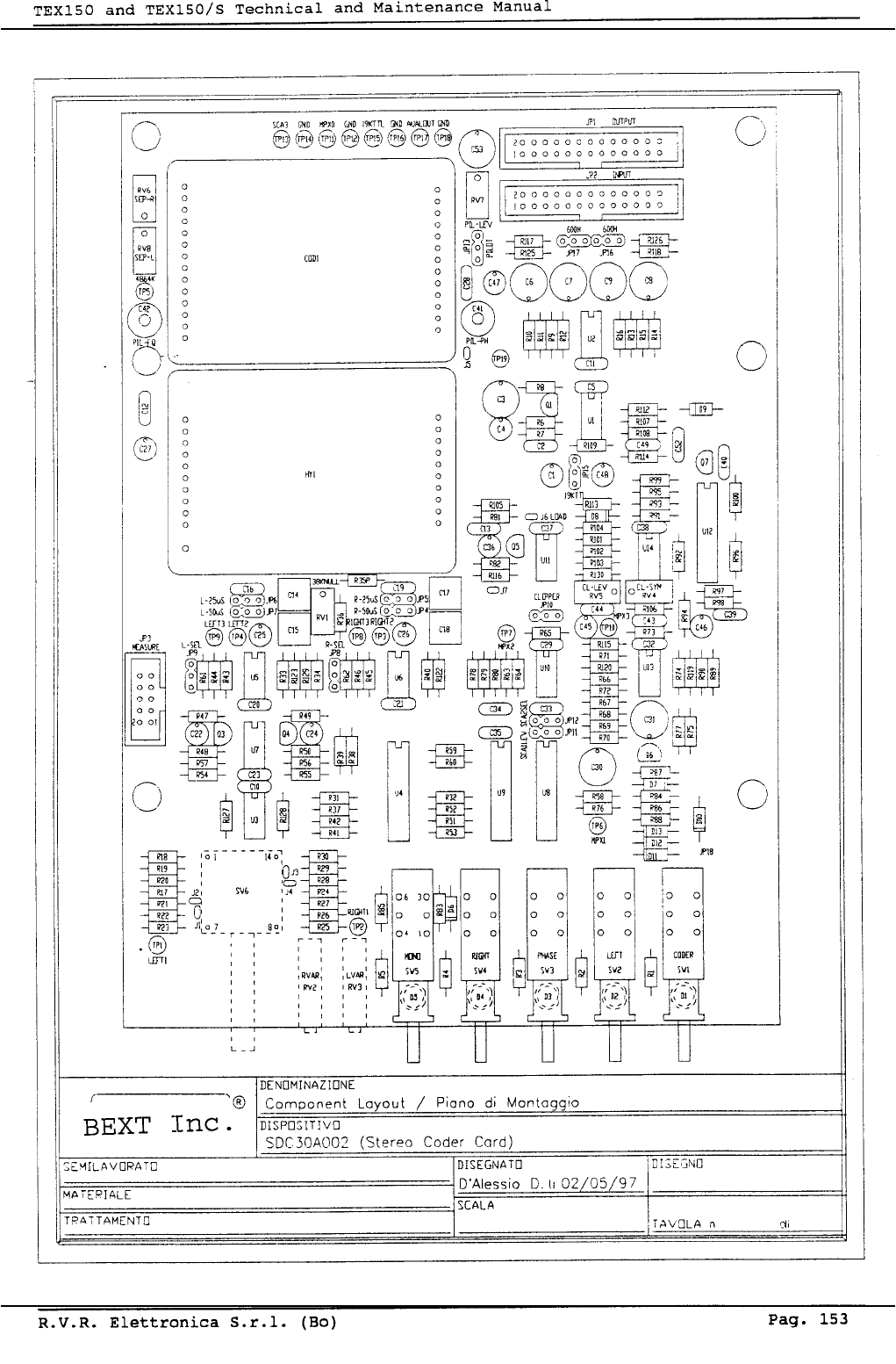
XT150 and XT150S Technical and Maintenance Manual
Pag. 150

XT150 and XT150S Technical and Maintenance Manual
Pag. 151
TCXO CARDTCXO CARD
TCXO CARDTCXO CARD
TCXO CARD
1 Circuit Diagram Pag. 152
2 Bill of Materials Pag. 153
3 Coponent Layout Pag. 154
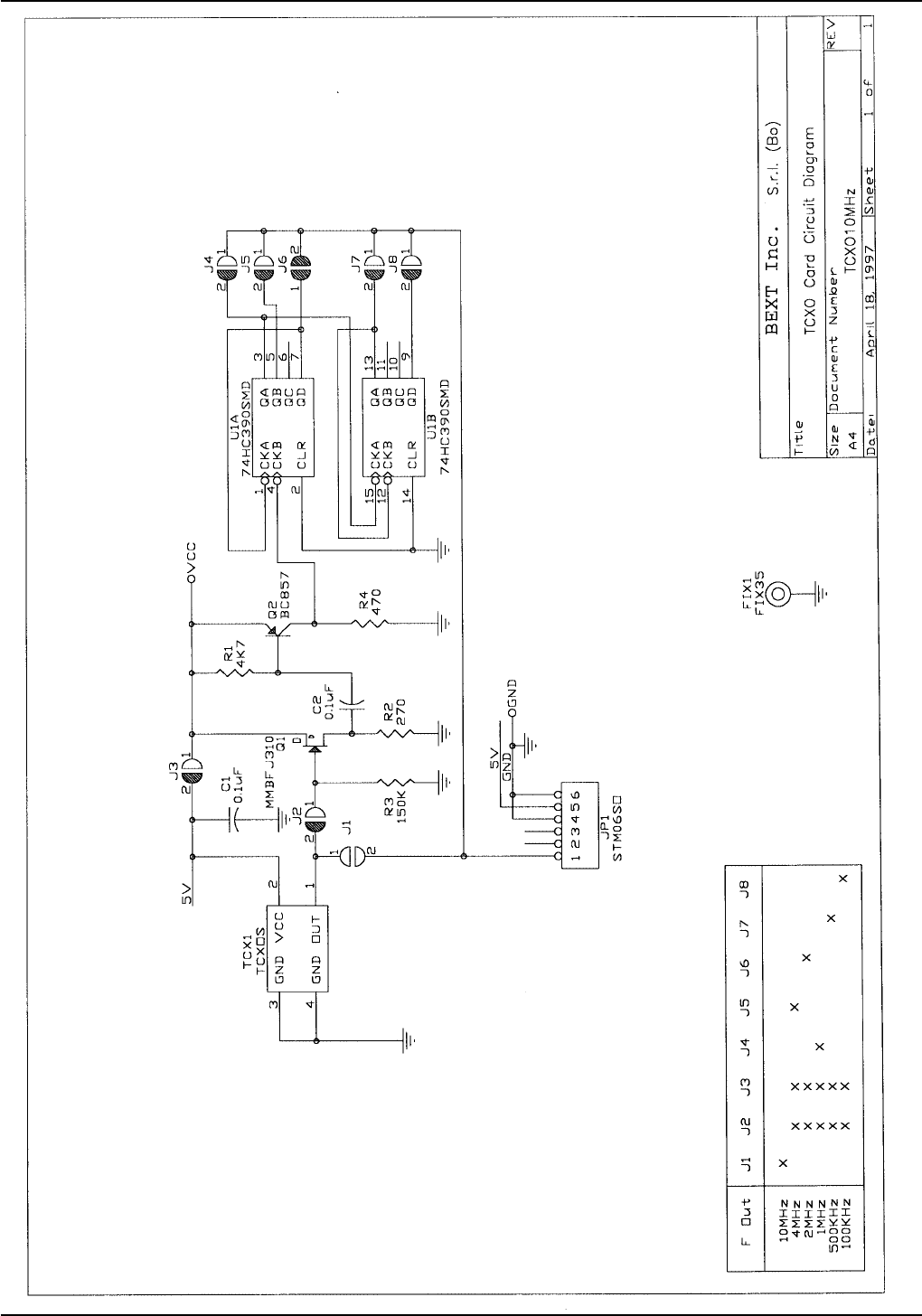
XT150 and XT150S Technical and Maintenance Manual
Pag. 152

XT150 and XT150S Technical and Maintenance Manual
Pag. 153
TCXO Card Bill Of Materials Page 1
Item Quantity Reference Part
____________________________________________________________________________________________________
1 2 C1,C2 0.1uF
2 1 FIX1 FIX35
3 1 JP1 STM06SO
4 8 J1,J2,J3,J4,J5,J6,J7,J8 JSMD
5 1 Q1 MMBFJ310
6 1 Q2 BC857
7 1 R1 4K7
8 1 R2 270
9 1 R3 150K
10 1 R4 470
11 1 TCX1 TCXOS
12 1 U1 74HC390SMD
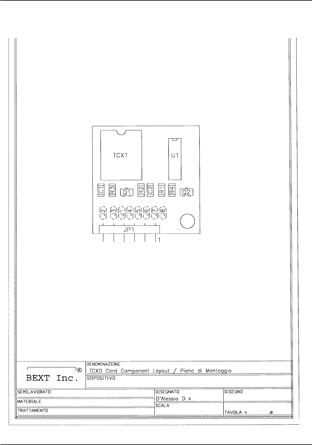
XT150 and XT150S Technical and Maintenance Manual
Pag. 154